WO2024209784A1 - 積層セラミックコンデンサ - Google Patents
積層セラミックコンデンサ Download PDFInfo
- Publication number
- WO2024209784A1 WO2024209784A1 PCT/JP2024/004131 JP2024004131W WO2024209784A1 WO 2024209784 A1 WO2024209784 A1 WO 2024209784A1 JP 2024004131 W JP2024004131 W JP 2024004131W WO 2024209784 A1 WO2024209784 A1 WO 2024209784A1
- Authority
- WO
- WIPO (PCT)
- Prior art keywords
- layer
- electrode
- disposed
- glass
- laminate
- Prior art date
- Legal status (The legal status is an assumption and is not a legal conclusion. Google has not performed a legal analysis and makes no representation as to the accuracy of the status listed.)
- Ceased
Links
Images


Classifications
-
- H—ELECTRICITY
- H01—ELECTRIC ELEMENTS
- H01G—CAPACITORS; CAPACITORS, RECTIFIERS, DETECTORS, SWITCHING DEVICES, LIGHT-SENSITIVE OR TEMPERATURE-SENSITIVE DEVICES OF THE ELECTROLYTIC TYPE
- H01G4/00—Fixed capacitors; Processes of their manufacture
- H01G4/30—Stacked capacitors
-
- H—ELECTRICITY
- H01—ELECTRIC ELEMENTS
- H01G—CAPACITORS; CAPACITORS, RECTIFIERS, DETECTORS, SWITCHING DEVICES, LIGHT-SENSITIVE OR TEMPERATURE-SENSITIVE DEVICES OF THE ELECTROLYTIC TYPE
- H01G4/00—Fixed capacitors; Processes of their manufacture
- H01G4/002—Details
- H01G4/005—Electrodes
- H01G4/012—Form of non-self-supporting electrodes
-
- H—ELECTRICITY
- H01—ELECTRIC ELEMENTS
- H01G—CAPACITORS; CAPACITORS, RECTIFIERS, DETECTORS, SWITCHING DEVICES, LIGHT-SENSITIVE OR TEMPERATURE-SENSITIVE DEVICES OF THE ELECTROLYTIC TYPE
- H01G4/00—Fixed capacitors; Processes of their manufacture
- H01G4/002—Details
- H01G4/018—Dielectrics
- H01G4/06—Solid dielectrics
- H01G4/08—Inorganic dielectrics
- H01G4/12—Ceramic dielectrics
-
- H—ELECTRICITY
- H01—ELECTRIC ELEMENTS
- H01G—CAPACITORS; CAPACITORS, RECTIFIERS, DETECTORS, SWITCHING DEVICES, LIGHT-SENSITIVE OR TEMPERATURE-SENSITIVE DEVICES OF THE ELECTROLYTIC TYPE
- H01G4/00—Fixed capacitors; Processes of their manufacture
- H01G4/002—Details
- H01G4/228—Terminals
- H01G4/232—Terminals electrically connecting two or more layers of a stacked or rolled capacitor
- H01G4/2325—Terminals electrically connecting two or more layers of a stacked or rolled capacitor characterised by the material of the terminals
-
- H—ELECTRICITY
- H01—ELECTRIC ELEMENTS
- H01G—CAPACITORS; CAPACITORS, RECTIFIERS, DETECTORS, SWITCHING DEVICES, LIGHT-SENSITIVE OR TEMPERATURE-SENSITIVE DEVICES OF THE ELECTROLYTIC TYPE
- H01G4/00—Fixed capacitors; Processes of their manufacture
- H01G4/002—Details
- H01G4/228—Terminals
- H01G4/252—Terminals the terminals being coated on the capacitive element
Definitions
- the present invention relates to a multilayer ceramic capacitor.
- an internal electrode layer is disposed inside a multilayer chip having a dielectric layer containing a ceramic material that functions as a dielectric.
- the internal electrode layer is exposed on the surface of the multilayer chip, and an external electrode is disposed so as to be joined to the internal electrode layer.
- a plating layer containing metals such as copper (Cu), nickel (Ni), and tin (Sn) as its main components is provided on the surface of the external electrode.
- Patent document 2 describes how hydrogen generated by a chemical reaction during the plating layer formation process is absorbed into the internal electrode, and the absorbed hydrogen gradually reduces the dielectric layer around the internal electrode, causing a deterioration in insulation resistance.
- JP 2022-119088 A Japanese Patent Application Publication No. 1-80011
- the purpose of the present invention is to suppress deterioration of insulation resistance in multilayer ceramic capacitors.
- the multilayer ceramic capacitor of the present invention comprises a laminate having a first surface and a second surface facing each other in the stacking direction, a third surface and a fourth surface facing each other in a first direction perpendicular to the stacking direction, and a fifth surface and a sixth surface facing each other in a second direction perpendicular to the stacking direction and the first direction, and an external electrode disposed on the fifth surface of the laminate.
- the laminate comprises an inner dielectric layer, and an inner layer portion having an internal electrode laminated on the inner dielectric layer in the stacking direction and having an end portion located on the fifth surface.
- the external electrode comprises an inner base electrode layer disposed on the inner layer portion on the fifth surface and connected to the internal electrode, an inner glass layer containing a glass component disposed on the inner base electrode layer, a plating layer disposed on the inner glass layer, and a connection portion extending through the inner glass layer and electrically connecting the inner base electrode layer and the plating layer.
- the present invention makes it possible to prevent deterioration of insulation resistance in multilayer ceramic capacitors.
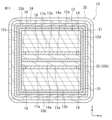
- FIG. 1 is a perspective view of a multilayer ceramic capacitor according to a first embodiment of the present invention
- 2 is a cross-sectional view taken along line II-II of FIG. 3 is a cross-sectional view taken along line III-III in FIG.
- FIG. 1 is an exploded perspective view of an inner layer portion according to a first embodiment of the present invention
- FIG. 3 is an enlarged view of region R in FIG.
- FIG. 5 is a perspective view of a multilayer ceramic capacitor according to a second embodiment of the present invention
- a cross-sectional view taken along line XX of FIG. 1 is a flowchart for explaining a method for manufacturing a multilayer ceramic capacitor according to a first embodiment of the present invention.
- each embodiment is an illustrative example of how the present invention can be implemented, and the present invention is not limited to the contents of the embodiment. It is also possible to combine the contents described in different embodiments, and the implementation in such cases is also included in the present invention.
- the drawings are intended to aid in understanding the specification, and may be drawn diagrammatically, and the dimensional ratios of the depicted components or between the components may not match those dimensional ratios described in the specification. Components described in the specification may be omitted in the drawings, or may be drawn with the number of components omitted.
- Multilayer ceramic capacitor (first embodiment) A laminated ceramic capacitor according to a first embodiment of the present invention will now be described.
- FIG. 1 is a perspective view showing an example of a multilayer ceramic capacitor according to a first embodiment of the present invention.
- FIG. 2 is a cross-sectional view taken along line II-II in FIG. 1.
- FIG. 3 is a cross-sectional view taken along line III-III in FIG. 1.
- the drawings may show the stacking direction X, width direction Y, and length direction Z of the multilayer ceramic capacitor 10, and these directions may be referred to in the following description.
- the width direction Y in this embodiment is an example of the first direction according to the present invention
- the length direction Z is an example of the second direction according to the present invention.
- the width direction Y in this embodiment may be an example of the second direction according to the present invention
- the length direction Z may be an example of the second direction according to the present invention.
- the multilayer ceramic capacitor 10 has a laminate 12, a first external electrode 30a, and a second external electrode 30b.
- the external electrode 30 when there is no need to distinguish between the first external electrode 30a and the second external electrode 30b, one of them may simply be referred to as the external electrode 30.
- the laminate 12 of this embodiment has a rectangular parallelepiped shape or a substantially rectangular parallelepiped shape as a whole.
- the laminate 12 has a first surface 12a and a second surface 12b that face each other in the stacking direction X, a third surface 12c and a fourth surface 12d that face each other in the width direction Y, and a fifth surface 12e and a sixth surface 12f that face each other in the length direction Z.
- the stacking direction X, the width direction Y, and the length direction Z are perpendicular to each other.
- the corners and ridges of the laminate 12 are rounded.
- the corners are the portions where three adjacent surfaces of the laminate 12 intersect.
- the ridges are the portions where two adjacent surfaces of the laminate 12 intersect.
- the first surface 12a and the second surface 12b, the third surface 12c and the fourth surface 12d, and the fifth surface 12e and the sixth surface 12f may have irregularities formed in part or all of them.
- the laminate 12 includes an inner layer 13, a first outer layer 16a, and a second outer layer 16b.
- the outer layer 16a when there is no need to distinguish between the first outer layer 16a and the second outer layer 16b, one of them may simply be referred to as the outer layer 16.
- the inner layer portion 13 has a plurality of inner electrodes 13a and a plurality of inner dielectric layers 14a.
- the inner layer portion 13 is a portion located between the inner electrode 13a among the plurality of inner electrodes 13a that is closest to the first outer layer portion 16a and the inner electrode 13a among the plurality of inner electrodes 13a that is closest to the second outer layer portion 16b.
- the inner layer portion 13 is a portion located between the inner electrode 13a adjacent to the first outer layer portion 16a and the inner electrode 13a adjacent to the second outer layer portion 16b.
- the multiple inner dielectric layers 14a are stacked in the stacking direction X. In other words, the multiple inner dielectric layers 14a are arranged side by side in the stacking direction X.
- the material of each inner dielectric layer 14a is arbitrary.
- a dielectric ceramic mainly composed of barium titanate (BaTiO 3 ) can be used as the material of the inner dielectric layer 14a.
- the material of the inner dielectric layer 14a may have multiple crystal grains containing a perovskite compound having BaTiO 3 as a basic structure.
- a dielectric ceramic mainly composed of another compound such as calcium titanate (CaTiO 3 ), strontium titanate (SrTiO 3 ), calcium zirconate (CaZrO 3 ), etc. may be used as the material of the inner dielectric layer 14a.
- the material for the inner dielectric layer 14a may be a material in which, as a subcomponent, a manganese (Mn) compound, an iron (Fe) compound, a chromium (Cr) compound, a cobalt (Co) compound, a nickel (Ni) compound, or the like is added to a main component such as BaTiO3, CaTiO3, SrTiO3, or CaZrO3 in a content range less than that of the main component.
- the thickness of the inner dielectric layer 14a that is, the dimension in the stacking direction X, is arbitrary, but is preferably, for example, 10.0 ⁇ m or less.
- Each internal electrode 13a is disposed between two adjacent dielectric layers in the stacking direction X among the multiple dielectric layers included in the laminate 12.
- the internal electrode 13a may be disposed between two adjacent inner layer dielectric layers 14a in the stacking direction X among the multiple inner layer dielectric layers 14a.
- the internal electrode 13a may be disposed between the inner layer dielectric layer 14a disposed adjacent to each other in the stacking direction X and the outer layer dielectric layer 17a of the outer layer portion 16.
- the inner layer dielectric layer 14a is disposed between the two internal electrodes 13a adjacent to each other in the stacking direction X.
- the internal electrode 13a is disposed in contact with the inner layer dielectric layer 14a.
- the internal electrode 13a in this embodiment is a plate-shaped electrode.
- the internal electrode 13a extends in the longitudinal direction Z.
- the internal electrode 13a has a first end exposed on either the fifth surface 12e or the sixth surface 12f, and a second end located inside the laminate 12.
- each internal electrode 13a is exposed on either the fifth surface 12e or the sixth surface 12f of the laminate 12.
- the multiple internal electrodes 13a include internal electrodes 13a exposed on the fifth surface 12e and not exposed on the sixth surface 12f, and internal electrodes 13a exposed on the sixth surface 12f and not exposed on the fifth surface 12e.
- the internal electrodes 13a exposed on the fifth surface 12e and not exposed on the sixth surface 12f and the internal electrodes 13a exposed on the sixth surface 12f and not exposed on the fifth surface 12e are arranged alternately in the stacking direction X.
- FIG. 4 is an exploded perspective view of the inner layer portion 13.
- each internal electrode 13a has an opposing electrode portion 15a and an extraction electrode portion 15b.
- the opposing electrode portion 15a is a portion of the internal electrode 13a that faces another adjacent internal electrode 13a in the stacking direction X.
- the extraction electrode portion 15b is a portion of the internal electrode 13a other than the opposing electrode portion 15a.
- the opposing electrode portions 15a of two internal electrodes 13a adjacent to each other in the stacking direction X face each other via the inner dielectric layer 14a, thereby forming a capacitance.
- Each extraction electrode portion 15b is exposed to either the fifth surface 12e or the sixth surface 12f.
- the shape of the internal electrode 13a is not particularly limited, but is preferably rectangular when viewed from the stacking direction X.
- the corners of the opposing electrode portion 15a may be chamfered or rounded.
- the corners of the extraction electrode portion 15b may be chamfered or rounded.
- the internal electrode 13a preferably has a uniform thickness along the width direction Y, i.e., a dimension in the stacking direction X.
- the thickness of the ends of the internal electrode 13a in the width direction Y may be thicker than the thickness of the center of the internal electrode 13a in the width direction Y.
- the main component of the internal electrode 13a is copper (Cu).
- the main component of the internal electrode 13a is optional, and may be other metals such as Ni, palladium (Pd), or silver (Ag) instead of Cu.
- the main component of the internal electrode 13a may also be an alloy of Ni, Pd, Ag, Cu, or another metal.
- the thickness of the internal electrode 13a is arbitrary, but it is preferable that it be, for example, 0.2 ⁇ m or more and 2.0 ⁇ m or less.
- the first outer layer portion 16a and the second outer layer portion 16b are arranged to sandwich the inner layer portion 13 in the stacking direction X.
- the first outer layer portion 16a is arranged on one side of the stacking direction X with respect to the inner layer portion 13 (upper side in FIG. 2). In other words, the first outer layer portion 16a is arranged on the first surface 12a side with respect to the inner layer portion 13.
- the second outer layer portion 16b is arranged on the other side of the stacking direction X with respect to the inner layer portion 13 (lower side in FIG. 2). In other words, the second outer layer portion 16b is arranged on the second surface 12b side with respect to the inner layer portion 13.
- the outer layer portion 16 has a plurality of outer dielectric layers 17a.
- the plurality of outer dielectric layers 17a are stacked in the stacking direction X.
- the material of each outer dielectric layer 17a is arbitrary.
- a dielectric ceramic mainly composed of BaTiO 3 can be used as the material of the outer dielectric layer 17a.
- a dielectric ceramic mainly composed of other compounds such as CaTiO 3 , SrTiO 3 , CaZrO 3 , etc. may be used as the material of the outer dielectric layer 17a.
- a compound such as a Mn compound, an Fe compound, a Cr compound, a Co compound, or a Ni compound may be added as an auxiliary component to the main component such as BaTiO 3, CaTiO 3 , SrTiO 3, or CaZrO 3 in a content range less than that of the main component.
- the material of the outer dielectric layer 17a may be formed from a main component different from that of the material of the inner dielectric layer 14a.
- an insulating layer may be disposed on the third surface 12c and the fourth surface 12d of the laminate 12.
- an insulating layer When an insulating layer is disposed, it is possible to suppress the intrusion of moisture into the interface between the internal electrode 13a and the inner dielectric layer 14a, the interface between the internal electrode 13a and the outer dielectric layer 17a, and into the interior of the laminate 12.
- the insulating layer has the same or similar components as the inner dielectric layer 14a or the outer dielectric layer 17a.
- the adhesion between the insulating layer and the inner dielectric layer 14a is improved.
- the insulating layer has the same or similar components as the outer dielectric layer 17a, the adhesion between the insulating layer and the outer dielectric layer 17a is improved.
- the insulating layer may also be arranged so as to be joined to the internal electrode 13a.
- the surface of the insulating layer that is not joined to the internal electrode 13a becomes the third surface 12c and the fourth surface 12d.
- the surface of the insulating layer that is arranged on the opposite side to the internal electrode 13a constitutes the third surface 12c and the fourth surface 12d of the laminate 12.
- the insulating layer preferably includes an inner layer that is the innermost in the width direction Y and an outer layer that is the outermost in the first direction.
- the insulating layer is not limited to a two-layer structure, but may be a three-layer or more structure.
- the layer located on the innermost side in the width direction Y is the inner layer
- the layer located on the outermost side in the width direction Y is the outer layer.
- the step layer 19 is disposed on the same plane as the internal electrode 13a. If the step layer 19 is not disposed, a difference in thickness occurs between the portion where the internal electrode 13a is disposed and the portion where the internal electrode 13a is not disposed, and distortion occurs during pressing during the manufacturing process of the multilayer ceramic capacitor 10 described below, which may result in a structural defect. In contrast, in this embodiment, the step layer 19 can fill the step of the thickness of the internal electrode 13a in the stacking direction X, so that distortion during pressing during the manufacturing process of the multilayer ceramic capacitor 10 can be alleviated and structural defects can be suppressed. It is preferable that the step layer 19 has the same or approximately the same thickness as the internal electrode 13a disposed on the same plane. It is preferable that the step layer 19 contains the same or approximately the same components as the inner dielectric layer 14a.
- the first external electrode 30a is disposed on the fifth surface 12e side of the laminate 12.
- the first external electrode 30a is disposed on the first surface 12a, the second surface 12b, the third surface 12c, the fourth surface 12d, and the fifth surface 12e.
- the first external electrode 30a may be disposed only on the fifth surface 12e of the laminate 12, but it is preferable that the first external electrode 30a is disposed continuously on the fifth surface 12e, the first surface 12a, and the second surface 12b. It is more preferable that the first external electrode 30a is also disposed on the third surface 12c and the fourth surface 12d.
- the first external electrode 30a is joined to the internal electrode 13a exposed on the fifth surface 12e of the laminate 12. As a result, the first external electrode 30a is electrically connected to the internal electrode 13a disposed on the fifth surface 12e of the laminate 12.
- the second external electrode 30b is disposed on the sixth surface 12f side of the laminate 12.
- the second external electrode 30b is disposed on the first surface 12a, the second surface 12b, the third surface 12c, the fourth surface 12d, and the sixth surface 12f.
- the second external electrode 30b may be disposed only on the sixth surface 12f of the laminate 12, but it is preferable that the second external electrode 30b is disposed continuously on the sixth surface 12f, the first surface 12a, and the second surface 12b. It is more preferable that the second external electrode 30b is also disposed on the third surface 12c and the fourth surface 12d.
- the second external electrode 30b is joined to the internal electrode 13a exposed on the sixth surface 12f of the laminate 12. As a result, the second external electrode 30b is electrically connected to the internal electrode 13a disposed on the sixth surface 12f of the laminate 12.
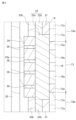
- FIG. 5 is an enlarged view of region R in FIG. 2.
- FIG. 5 shows an enlarged view of a portion of the first external electrode 30a, but the second external electrode 30b has a similar configuration to the first external electrode 30a.
- the external electrode 30 comprises a glass layer 31 and an underlying electrode layer 32 arranged to cover the glass layer 31.
- the external electrode 30 comprises an inner glass layer 33a and an outer glass layer 33b arranged on the underlying electrode layer 32, a plating layer 34 arranged on the inner glass layer 33a and the outer glass layer 33b, and a surface plating layer 35 arranged on the plating layer 34.
- the glass layer 31 is composed of a glass component.
- the glass component includes at least one selected from boron (B), silicon (Si), barium (Ba), magnesium (Mg), aluminum (Al), and lithium (Li).
- B boron
- Si silicon
- Ba barium
- Mg magnesium
- Al aluminum
- Li lithium
- the glass layer 31 is disposed at a position overlapping with the outer layer portion 16 when the laminate 12 is viewed along the longitudinal direction Z.
- the glass layer 31 is disposed on both sides (upper and lower sides in FIG. 2 ) of an inner layer base electrode layer 32a described later in the lamination direction X.
- the glass layer 31 of the first external electrode 30a is disposed on the fifth surface 12e side of the laminate 12.
- the glass layer 31 of the first external electrode 30a is disposed continuously on the first surface 12a, the second surface 12b, the third surface 12c, the fourth surface 12d, and the fifth surface 12e of the laminate 12.
- the glass layer 31 of the first external electrode 30a may be disposed only on the fifth surface 12e of the laminate 12, but is preferably disposed continuously on the fifth surface 12e, the first surface 12a, and the second surface 12b. It is preferable that the glass layer 31 of the first external electrode 30a is also disposed on the third surface 12c and the fourth surface 12d.
- the glass layer 31 of the first external electrode 30a is disposed on the outer layer 16 on the fifth surface 12e of the laminate 12.
- the glass layer 31 of the first external electrode 30a is disposed on the outer dielectric layer 17a.
- the glass layer 31 of the first external electrode 30a is not connected to the internal electrode 13a exposed on the fifth surface 12e of the laminate 12, but may be connected to the internal electrode 13a.
- the glass layer 31 of the first external electrode 30a is thinner at the end portion on the first surface 12a and the second surface 12b toward the center of the laminate 12 in the length direction Z than the other portions.
- it is preferable that the glass layer 31 of the first external electrode 30a is thinner at the end portion on the third surface 12c and the fourth surface 12d toward the center in the length direction Z than the other portions.
- the glass layer 31 of the second external electrode 30b is disposed on the sixth surface 12f side of the laminate 12.
- the glass layer 31 of the second external electrode 30b is disposed continuously on the first surface 12a, the second surface 12b, the third surface 12c, the fourth surface 12d, and the sixth surface 12f of the laminate 12.
- the glass layer 31 of the second external electrode 30b may be disposed only on the sixth surface 12f of the laminate 12, but is preferably disposed continuously on the sixth surface 12f, the first surface 12a, and the second surface 12b. It is preferable that the glass layer 31 of the second external electrode 30b is also disposed on the third surface 12c and the fourth surface 12d.
- the glass layer 31 of the second external electrode 30b is disposed on the outer layer 16 on the sixth surface 12f of the laminate 12.
- the glass layer 31 of the second external electrode 30b is disposed on the outer dielectric layer 17a.
- the glass layer 31 of the second external electrode 30b is not connected to the internal electrode 13a exposed on the sixth surface 12f of the laminate 12, but may be connected to the internal electrode 13a.
- the glass layer 31 of the second external electrode 30b is thinner at the end portion on the first surface 12a and the second surface 12b toward the center of the laminate 12 in the length direction Z than the other portions.
- it is preferable that the glass layer 31 of the first external electrode 30a is thinner at the end portion on the third surface 12c and the fourth surface 12d toward the center in the length direction Z than the other portions.
- the base electrode layer 32 is made of a baking layer.
- the baking layer contains a glass component and a metal.
- the glass component contained in the baking layer contains at least one selected from B, Si, Ba, Mg, Al, and Li.
- the glass component contained in the baking layer is silicon dioxide (SiO 2 ) to which at least one selected from B, Ba, Mg, Al, and Li has been added.
- the glass component contains Al, Ba, and O in addition to Si.
- the metal contained in the baking layer contains at least one selected from, for example, Cu, Ni, Ag, Pd, an Ag-Ni alloy, and gold (Au).
- the base electrode layer 32 has an inner layer base electrode layer 32a and an outer layer base electrode layer 32b.
- the inner layer base electrode layer 32a overlaps with the inner layer portion 13 when the base electrode layer 32 is viewed along the longitudinal direction Z.
- the outer layer base electrode layer 32b overlaps with the outer layer portion 16 when the base electrode layer 32 is viewed along the longitudinal direction Z.
- the outer layer base electrode layer 32b is disposed on the glass layer 31.
- the outer layer base electrode layer 32b is disposed so as to cover the glass layer 31 from the outside in the longitudinal direction Z.
- the inner layer base electrode layer 32a of the first external electrode 30a is disposed on the inner layer portion 13 on the fifth surface 12e of the laminate 12.
- the inner layer base electrode layer 32a of the first external electrode 30a is connected to the internal electrode 13a exposed on the fifth surface 12e of the laminate 12.
- the inner layer base electrode layer 32a of the first external electrode 30a is electrically connected to the internal electrode 13a disposed on the fifth surface 12e of the laminate 12.
- the inner layer base electrode layer 32a of the second external electrode 30b is disposed on the inner layer portion 13 on the sixth surface 12f of the laminate 12.
- the inner layer base electrode layer 32a of the second external electrode 30b is connected to the internal electrode 13a exposed on the sixth surface 12f of the laminate 12.
- the inner layer base electrode layer 32a of the second external electrode 30b is electrically connected to the internal electrode 13a disposed on the sixth surface 12f of the laminate 12.
- the outer layer base electrode layer 32b of the first external electrode 30a is continuously arranged at a position facing the fifth surface 12e, the first surface 12a, the second surface 12b, the third surface 12c, and the fourth surface 12d of the laminate 12.
- the outer layer base electrode layer 32b of the first external electrode 30a may be arranged at a position facing only the fifth surface 12e of the laminate 12, but it is preferable that it is also continuously arranged at a position facing the first surface 12a and the second surface 12b. It is preferable that the outer layer base electrode layer 32b of the first external electrode 30a is also arranged at a position facing the third surface 12c and the fourth surface 12d.
- the outer layer base electrode layer 32b of the first external electrode 30a is connected to the inner layer base electrode layer 32a of the first external electrode 30a.
- the outer layer base electrode layer 32b of the first external electrode 30a is electrically connected to the internal electrode 13a exposed on the fifth surface 12e of the laminate 12.
- the outer layer base electrode layer 32b of the first external electrode 30a may be disposed between the third surface 12c or the fourth surface 12d and the internal electrode 13a.
- the outer layer base electrode layer 32b of the second external electrode 30b in this embodiment is continuously arranged at a position facing the sixth surface 12f, the first surface 12a, the second surface 12b, the third surface 12c, and the fourth surface 12d of the laminate 12.
- the outer layer base electrode layer 32b of the second external electrode 30b may be arranged at a position facing only the sixth surface 12f of the laminate 12, but it is preferable that it is continuously arranged at a position facing the first surface 12a and the second surface 12b. It is preferable that the outer layer base electrode layer 32b of the second external electrode 30b is also arranged at a position facing the third surface 12c and the fourth surface 12d.
- the outer layer base electrode layer 32b of the second external electrode 30b is connected to the inner layer base electrode layer 32a of the second external electrode 30b.
- the outer layer base electrode layer 32b of the second external electrode 30b is electrically connected to the internal electrode 13a exposed on the sixth surface 12f of the laminate 12.
- the outer layer base electrode layer 32b of the second external electrode 30b may be disposed between the third surface 12c or the fourth surface 12d and the internal electrode 13a.
- the inner glass layer 33a is composed of a glass component.
- the glass component includes at least one selected from B, Si, Ba, Mg, Al, and Li.
- at least one selected from B, Ba, Mg, Al, and Li is added to silicon dioxide (SiO 2 ).
- the inner glass layer 33a is disposed on the inner base electrode layer 32a. In other words, the inner glass layer 33a is disposed at a position overlapping the inner base electrode layer 32a when viewed along the length direction Z. In other words, the inner glass layer 33a is disposed so as to cover the inner base electrode layer 32a.
- the area in which the inner base electrode layer 32a and the plating layer 34 are alloyed together when the plating layer 34 is formed is reduced. This reduces the amount of hydrogen absorbed by the internal electrodes 13a, making it possible to suppress deterioration of the insulation resistance.
- the thickness of the inner glass layer 33a i.e., the dimension in the longitudinal direction Z of the laminate 12, is preferably 0.2 ⁇ m or more and 3.5 ⁇ m or less. By making it thicker than 0.2 ⁇ m, it is possible to further suppress the absorption of hydrogen that occurs when forming the plating layer 34, and if it is thinner than 3.5 ⁇ m, it is possible to suppress the time required to form the connection part 36 described below.
- the outer glass layer 33b is composed of a glass component.
- the glass component includes at least one selected from B, Si, Ba, Mg, Al, and Li.
- at least one selected from B, Ba, Mg, Al, and Li is added to silicon dioxide (SiO 2 ).
- the outer glass layer 33b is disposed on the outer base electrode layer 32b. In other words, the outer glass layer 33b is disposed at a position overlapping with the outer base electrode layer 32b when viewed along the length direction Z. In other words, the outer glass layer 33b is disposed so as to cover the outer base electrode layer 32b.
- the region on the outer base electrode layer 32b side from a position 5 ⁇ m toward the inner base electrode layer 32a in the stacking direction X from the boundary between the inner base electrode layer 32a and the outer base electrode layer 32b is the outer glass layer 33b.
- the outer glass layer 33b extends toward the tip of the outer electrode 30 along the shape of the outer electrode 30.
- the tip of the outer glass layer 33b may have a tapered shape, and may not reach the tip of the outer electrode 30.
- the outer glass layer 33b of the first external electrode 30a in this embodiment is continuously arranged at a position facing the fifth surface 12e, the first surface 12a, the second surface 12b, the third surface 12c, and the fourth surface 12d of the laminate 12.
- the outer glass layer 33b of the first external electrode 30a may be arranged only on the fifth surface 12e of the laminate 12, but it is preferable that it is also continuously arranged on the first surface 12a and the second surface 12b. It is preferable that the outer glass layer 33b of the first external electrode 30a is also arranged on the third surface 12c and the fourth surface 12d.
- the outer glass layer 33b of the second external electrode 30b in this embodiment is continuously arranged at a position facing the sixth surface 12f, the first surface 12a, the second surface 12b, the third surface 12c, and the fourth surface 12d of the laminate 12.
- the outer glass layer 33b of the second external electrode 30b may be arranged only on the sixth surface 12f of the laminate 12, but it is preferable that it is also continuously arranged on the first surface 12a and the second surface 12b. It is preferable that the outer glass layer 33b of the second external electrode 30b is also arranged on the third surface 12c and the fourth surface 12d.
- the thickness of the outer glass layer 33b in a direction perpendicular to the laminate 12 is thinner than the thickness of the inner glass layer 33a in a direction perpendicular to the laminate 12.
- the thickness of the portion of the outer glass layer 33b arranged opposite the first surface 12a is the thickness in the direction perpendicular to the first surface 12a, i.e., the thickness in the stacking direction X.
- the thickness of the portion of the inner glass layer 33a arranged opposite the first surface 12a is the thickness in the direction perpendicular to the first surface 12a, i.e., the thickness in the stacking direction X.
- the thickness of the portion of the outer glass layer 33b arranged opposite the fifth surface 12e or the sixth surface 12f is the thickness in the direction perpendicular to the fifth surface 12e or the sixth surface 12f, i.e., the thickness in the length direction Z.
- the thickness of the portion of the laminate 12 of the inner glass layer 33a that is disposed opposite the fifth surface 12e or the sixth surface 12f is the thickness in the direction perpendicular to the fifth surface 12e or the sixth surface 12f, that is, the length direction Z.
- the plating layer 34 is disposed so as to cover the inner glass layer 33a and the outer glass layer 33b.
- the plating layer 34 is disposed on the inner glass layer 33a and the outer glass layer 33b.
- the plating layer 34 is a Ni plating layer.
- the main component of the plating layer 34 is Ni.
- the surface plating layer 35 is disposed so as to cover the plating layer 34.
- the surface plating layer 35 is disposed on the plating layer 34.
- the surface plating layer 35 is a Sn plating layer.
- the main component of the surface plating layer 35 is Sn.
- the external electrode 30 has a connection portion 36 that extends through the inner glass layer 33a and electrically connects the inner base electrode layer 32a and the plating layer 34.
- connection portion 36 is composed of the same components as the plating layer 34. That is, if the plating layer 34 is a Ni plating layer, the connection portion 36 is composed of Ni. If the plating layer 34 is a Sn plating layer, the connection portion 36 is composed of Sn. The presence of the connection portion 36 makes it possible to form a uniform plating layer 34 on the inner glass layer 33a in a short time, and also shortens the current path, which leads to a reduction in the electrical resistance of the multilayer ceramic capacitor 10.
- connection portion 36 can be confirmed by observing a cross section obtained when the laminate 12 is cross-sectionally polished in the width direction Y, i.e., a cross section including the stacking direction X and the length direction Z.
- the connection portion 36 has a columnar shape, but is not limited to this and may have a shape extending in the width direction Y. In that case, it can be confirmed by observing a cross section obtained when the laminate 12 is cross-sectionally polished in the stacking direction X, i.e., a cross section including the width direction Y and the length direction Z.
- the inner-layer base electrode layer 32a preferably satisfies the relationship of glass component area/(glass component area+metal component area) ⁇ 0.2.
- the area of the glass component contained in the inner-layer base electrode layer 32a is preferably 20% or less of the sum of the area of the glass component and the area of the metal component contained in the inner-layer base electrode layer 32a.
- the inner-layer base electrode layer 32a is an inner-layer base electrode layer 32a with a high density of the metal component, and therefore, the intrusion of moisture into the internal electrode 13a can be suppressed.
- the area of the glass component/(area of the glass component + area of the metal component) is measured, for example, as follows:
- the multilayer ceramic capacitor 10 is polished in the width direction Y to 1/2 of its dimension in the width direction Y. If an internal electrode 13a is present, it may be polished to 1/3 rather than 1/2.
- a position 1.5 ⁇ m away from the laminate 12 in the length direction Z from the internal electrode 13a closest to the outer layer 16 is set as the reference position.
- the glass area ratio is obtained in a range 20 ⁇ m from the reference position towards the center of the laminate 12 in the stacking direction X, and 2.0 ⁇ m away from the laminate 12 in the length direction Z from the reference position.
- the glass area ratio is calculated by, for example, binarizing the glass and metal components using image processing software (e.g., ImageJ from the National Institutes of Health) on an image measured using a FE-SEM (Field Emission Scanning Electron Microscope) at a magnification of 2000 times, an acceleration voltage of 15.0 kV, and a WD of 7.5 mm.
- image processing software e.g., ImageJ from the National Institutes of Health
- FE-SEM Field Emission Scanning Electron Microscope
- the multilayer ceramic capacitor 10 according to this embodiment can provide the following advantages.
- the inner glass layer 33a containing glass components is disposed on the inner base electrode layer 32a, the area in which the inner base electrode layer 32a and the plating layer 34 are alloyed is reduced when the plating layer 34 is formed. This reduces the amount of hydrogen absorbed by the internal electrode 13a, and suppresses deterioration of the insulation resistance.
- the thickness of the inner glass layer 33a containing the glass component of the external electrode in the longitudinal direction of the laminate 12 is preferably 0.2 ⁇ m or more and 3.5 ⁇ m or less. By making it thicker than 0.2 ⁇ m, the absorption of hydrogen that occurs when forming the plating layer 34 can be further suppressed, and if it is less than 3.5 ⁇ m, the time required to form the connection part 36 can be prevented from becoming longer.
- the external electrode 30 has a connection portion 36 that extends through the inner glass layer 33a and electrically connects the inner base electrode layer 32a and the plating layer 34.
- the presence of the connection portion 36 makes it possible to form a uniform plating layer 34 on the inner glass layer 33a in a short time, and also shortens the current path, which leads to a reduction in the electrical resistance of the multilayer ceramic capacitor 10.
- the thickness of the inner glass layer 33a containing the glass component of the external electrode 30 in the longitudinal direction Z of the laminate 12 is 0.2 ⁇ m or more and 3.5 ⁇ m or less. This configuration allows the plating layer 34 to be formed efficiently while further suppressing hydrogen absorption.
- the inner layer base electrode layer 32a has a glass area/(glass area + metal component area) ⁇ 0.2. With this configuration, the inner layer base electrode layer 32a has a high density of metal components, so that the intrusion of moisture into the internal electrode 13a can be suppressed.
- the multilayer ceramic capacitor according to the second embodiment has the same configuration as the multilayer ceramic capacitor according to the first embodiment, except for the shape and arrangement of the first internal electrodes, the shape and arrangement of the second internal electrodes, and the number and configuration of the external electrodes.
- the same or similar components as those in the first embodiment are denoted by the same or similar reference symbols, and detailed descriptions thereof will be omitted.
- FIG. 6 is a perspective view of the multilayer ceramic capacitor 110 according to this embodiment.
- FIG. 7 is a cross-sectional view taken along line VII-VII in FIG. 6.
- FIG. 8 is a cross-sectional view taken along line VIII-VIII in FIG. 6.
- the multilayer ceramic capacitor 110 of this embodiment includes a laminate 112 and four external electrodes 130a, 130b, 130c, and 130d.
- the external electrode 130 when there is no need to distinguish between the four external electrodes 130a, 130b, 130c, and 130d, one of the four external electrodes 130a, 130b, 130c, and 130d may simply be referred to as the external electrode 130.
- the internal electrode of this embodiment has a first internal electrode 113a and a second internal electrode 113b.
- the first internal electrode 113a has an opposing electrode portion 115a and two lead electrode portions 115b.
- Each lead electrode portion 115b is exposed to either the fifth surface 112e or the sixth surface 112f.
- the second internal electrode 113b has an opposing electrode portion 115c and two lead electrode portions 115d.
- Each lead electrode portion 115d is exposed to either the third surface 112c or the fourth surface 112d.
- the first internal electrode 113a and the second internal electrode 113b are arranged in the stacking direction X, sandwiching the inner dielectric layer 14a.
- the external electrodes 130 are arranged on each of the four sides of the laminate 112 when the laminate 112 is viewed along the lamination direction X.
- the first external electrode 130a and the second external electrode 130b are arranged to cover a part of the first surface 112a, a part of the second surface 112b, a part of the third surface 112c and the fourth surface 112d, and the fifth surface 112e or the sixth surface 112f of the laminate 112.
- the first external electrode 130a and the second external electrode 130b are electrically connected to the first internal electrode 113a.
- the third external electrode 130c and the fourth external electrode 130d are arranged to cover a part of the first surface 112a, a part of the second surface 112b, and the third surface 112c or the fourth surface 112d of the laminate 112.
- the third external electrode 130c and the fourth external electrode 130d are electrically connected to the second internal electrode 113b.
- the external electrode 130 has a similar configuration to the external electrode 30 according to the first embodiment. As shown in FIGS. 7, 8, 9, and 10, the external electrode 130 includes a glass layer 31 and an underlying electrode layer 32 arranged to cover the glass layer 31.
- the external electrode 130 includes an inner glass layer 33a and an outer glass layer 33b arranged on the underlying electrode layer 32, a plating layer 34 arranged on the inner glass layer 33a and the outer glass layer 33b, and a surface plating layer 35 arranged on the plating layer 34.
- the underlying electrode layer 32 of the external electrodes 130a and 130b is an example of a first underlying electrode layer according to the present disclosure
- the underlying electrode layer 32 of the external electrodes 130c and 130d is an example of a second underlying electrode layer according to the present disclosure.
- the inner glass layer 33a of the external electrodes 130a and 130b is an example of a first inner glass layer according to the present disclosure
- the inner glass layer 33a of the external electrodes 130c and 130d is an example of a second inner glass layer according to the present disclosure
- the plating layer 34 of the external electrodes 130a and 130b is an example of a first plating layer according to the present disclosure
- the plating layer 34 of the external electrodes 130c and 130d is an example of a second plating layer according to the present disclosure.
- each of the four external electrodes 130a, 130b, 130c, and 130d has the above configuration, that is, a configuration similar to that of the external electrode 30 according to the first embodiment, but is not limited to this.
- two external electrodes 130 arranged in opposing positions may have the above configuration. Only the external electrodes 130a and 130b may have the above configuration, or only the external electrodes 130c and 130d may have the above configuration.
- the base electrode layer 32 has an inner layer base electrode layer 32a and an outer layer base electrode layer 32b.
- the inner layer base electrode layer 32a overlaps with the inner layer portion 13 when the base electrode layer 32 is viewed along the length direction Z or the width direction Y.
- the outer layer base electrode layer 32b overlaps with the outer layer portion 16 when the base electrode layer 32 is viewed along the length direction Z or the width direction Y.
- the outer layer base electrode layer 32b is disposed on the glass layer 31.
- the outer layer base electrode layer 32b is disposed so as to cover the glass layer 31 from the outside in the length direction Z.
- the external electrode 130 has a connection portion 36 that extends through the inner glass layer 33a and electrically connects the inner base electrode layer 32a and the plating layer 34.
- the connection portion 36 of the external electrodes 130a, 130b is an example of a first connection portion according to the present disclosure
- the connection portion 36 of the external electrodes 130c, 130d is an example of a second connection portion according to the present disclosure.
- the configuration of the external electrode 30 of the multilayer ceramic capacitor 10 according to the first embodiment is applied to the external electrode 130 to which a positive potential is applied among the four external electrodes 130a, 130b, 130c, and 130d, the same effect as the multilayer ceramic capacitor 10 according to the first embodiment is achieved. Also, if the configuration of the external electrode 30 of the multilayer ceramic capacitor 10 according to the first embodiment is applied to all four external electrodes 130a, 130b, 130c, and 130d, such as the first external electrode 130a and the second external electrode 130b, the same effect as the multilayer ceramic capacitor 10 according to the first embodiment is achieved.
- Fig. 11 is a flowchart for explaining the manufacturing method of a multilayer ceramic capacitor.
- the manufacturing method of the multilayer ceramic capacitor 10 according to the first embodiment will be described as an example.
- the multilayer ceramic capacitor 110 according to the second embodiment can be manufactured by the same manufacturing method as the manufacturing method of the multilayer ceramic capacitor 10 according to the first embodiment.
- step S1 a dielectric sheet, a conductive paste for the internal electrodes, and a conductive paste for the external electrodes are prepared.
- the dielectric sheet, the conductive paste for the internal electrodes, and the conductive paste for the external electrodes contain a binder and a solvent.
- step S2 a conductive paste for the internal electrodes is printed in a predetermined pattern on the dielectric sheet, thereby forming a dielectric sheet for the inner layer portion on which the internal electrode pattern of the inner layer portion 13 is printed.
- the printing of the conductive paste for the internal electrodes on the dielectric sheet may be performed by, for example, screen printing or gravure printing.
- step S3 the dielectric sheet and the dielectric sheet for the internal electrode are stacked, and pressed in the stacking direction, for example, by a hydrostatic press, to form a laminated block.
- step S4 the laminated block is cut to a predetermined size to produce laminated chips.
- the corners and edges of the laminated chips may be rounded by barrel polishing or the like.
- step S5 the laminated chip is fired to form the laminate 12 according to this embodiment.
- step S6 a conductive paste containing a glass component and a metal is applied to the third surface 12c to the sixth surface 12f, for example, by a dipping method or a method of applying the conductive paste by extruding it from a slit plate. Then, a baking process is performed to form the glass layer 31, the inner layer base electrode layer 32a, the outer layer base electrode layer 32b, the inner layer glass layer 33a, and the outer layer glass layer 33b.
- the thickness of the inner glass layer 33a can be increased by increasing the content of glass components in the conductive paste containing glass components. In addition, the thickness of the inner glass layer 33a can be increased by increasing the temperature during the baking process.
- step S7 the glass layer 31, the inner layer base electrode layer 32a, the outer layer base electrode layer 32b, the inner layer glass layer 33a, and the outer layer glass layer 33b formed in step S6 are immersed in a glass dissolving liquid, thereby forming a crack in the inner layer glass layer 33a. This crack is formed so as to extend through the inner layer glass layer 33a in the thickness direction.
- step S8 the plating layer 34 is formed so that the plating layer 34 is connected to the inner layer base electrode layer 32a and the outer layer base electrode layer 32b.
- electrolytic plating is preferably used.
- barrel plating is preferably used. At this time, the nickel for forming the plating layer 34 flows through the cracks formed in step S7 to form the connection portion 36.
- the glass layer 31, the inner layer base electrode layer 32a, the outer layer base electrode layer 32b, the inner layer glass layer 33a, and the outer layer glass layer 33b are arranged on the third to sixth surfaces in step S6.
- the glass layer 31, the base electrode layer 32, the inner layer glass layer 33a, and the outer layer glass layer 33b arranged on a desired surface among the third to sixth surfaces are selectively immersed in a glass dissolving solution, thereby forming the external electrode according to the present invention on the desired surface.
- the step layer 19 is arranged on the same plane as the internal electrode 13a, but the step layer 19 does not have to be arranged on the same plane as the internal electrode 13a.
- the step layer 19 is arranged on the same plane as the first internal electrode 113a and the second internal electrode 113b, but the step layer 19 does not have to be arranged on the same plane as the first internal electrode 113a and the second internal electrode 113b. In other words, the step layer 19 does not have to be provided in the inner layer portion 13.
Landscapes
- Engineering & Computer Science (AREA)
- Power Engineering (AREA)
- Manufacturing & Machinery (AREA)
- Microelectronics & Electronic Packaging (AREA)
- Chemical & Material Sciences (AREA)
- Ceramic Engineering (AREA)
- Inorganic Chemistry (AREA)
- Fixed Capacitors And Capacitor Manufacturing Machines (AREA)
- Ceramic Capacitors (AREA)
Priority Applications (4)
| Application Number | Priority Date | Filing Date | Title |
|---|---|---|---|
| CN202480012757.4A CN120642013A (zh) | 2023-04-07 | 2024-02-07 | 层叠陶瓷电容器 |
| KR1020257027448A KR20250136382A (ko) | 2023-04-07 | 2024-02-07 | 적층 세라믹 콘덴서 |
| JP2025512423A JPWO2024209784A1 (https=) | 2023-04-07 | 2024-02-07 | |
| US19/298,502 US20250372311A1 (en) | 2023-04-07 | 2025-08-13 | Multilayer ceramic capacitor |
Applications Claiming Priority (2)
| Application Number | Priority Date | Filing Date | Title |
|---|---|---|---|
| JP2023062812 | 2023-04-07 | ||
| JP2023-062812 | 2023-04-07 |
Related Child Applications (1)
| Application Number | Title | Priority Date | Filing Date |
|---|---|---|---|
| US19/298,502 Continuation US20250372311A1 (en) | 2023-04-07 | 2025-08-13 | Multilayer ceramic capacitor |
Publications (1)
| Publication Number | Publication Date |
|---|---|
| WO2024209784A1 true WO2024209784A1 (ja) | 2024-10-10 |
Family
ID=92971850
Family Applications (1)
| Application Number | Title | Priority Date | Filing Date |
|---|---|---|---|
| PCT/JP2024/004131 Ceased WO2024209784A1 (ja) | 2023-04-07 | 2024-02-07 | 積層セラミックコンデンサ |
Country Status (5)
| Country | Link |
|---|---|
| US (1) | US20250372311A1 (https=) |
| JP (1) | JPWO2024209784A1 (https=) |
| KR (1) | KR20250136382A (https=) |
| CN (1) | CN120642013A (https=) |
| WO (1) | WO2024209784A1 (https=) |
Citations (3)
| Publication number | Priority date | Publication date | Assignee | Title |
|---|---|---|---|---|
| JP2010027730A (ja) * | 2008-07-16 | 2010-02-04 | Tdk Corp | セラミック積層電子部品およびその製造方法 |
| JP2017168746A (ja) * | 2016-03-17 | 2017-09-21 | 株式会社村田製作所 | 電子部品及び電子部品の製造方法 |
| JP2021158258A (ja) * | 2020-03-27 | 2021-10-07 | 株式会社村田製作所 | 積層セラミック電子部品 |
Family Cites Families (2)
| Publication number | Priority date | Publication date | Assignee | Title |
|---|---|---|---|---|
| JPH0630318B2 (ja) | 1987-09-21 | 1994-04-20 | 株式会社村田製作所 | 積層セラミックコンデンサ |
| JP7569131B2 (ja) | 2021-02-03 | 2024-10-17 | 太陽誘電株式会社 | セラミック電子部品およびその製造方法 |
-
2024
- 2024-02-07 KR KR1020257027448A patent/KR20250136382A/ko active Pending
- 2024-02-07 WO PCT/JP2024/004131 patent/WO2024209784A1/ja not_active Ceased
- 2024-02-07 CN CN202480012757.4A patent/CN120642013A/zh active Pending
- 2024-02-07 JP JP2025512423A patent/JPWO2024209784A1/ja active Pending
-
2025
- 2025-08-13 US US19/298,502 patent/US20250372311A1/en active Pending
Patent Citations (3)
| Publication number | Priority date | Publication date | Assignee | Title |
|---|---|---|---|---|
| JP2010027730A (ja) * | 2008-07-16 | 2010-02-04 | Tdk Corp | セラミック積層電子部品およびその製造方法 |
| JP2017168746A (ja) * | 2016-03-17 | 2017-09-21 | 株式会社村田製作所 | 電子部品及び電子部品の製造方法 |
| JP2021158258A (ja) * | 2020-03-27 | 2021-10-07 | 株式会社村田製作所 | 積層セラミック電子部品 |
Also Published As
| Publication number | Publication date |
|---|---|
| KR20250136382A (ko) | 2025-09-16 |
| JPWO2024209784A1 (https=) | 2024-10-10 |
| US20250372311A1 (en) | 2025-12-04 |
| CN120642013A (zh) | 2025-09-12 |
Similar Documents
| Publication | Publication Date | Title |
|---|---|---|
| JP7081543B2 (ja) | 積層セラミックコンデンサ | |
| JP7516709B2 (ja) | 積層セラミック電子部品 | |
| US12322551B2 (en) | Multilayer ceramic capacitor | |
| JP2025105529A (ja) | 積層型電子部品 | |
| JP2022091960A (ja) | 積層型キャパシタ及びその実装基板 | |
| WO2024161743A1 (ja) | 積層セラミックコンデンサ | |
| JP2023167525A (ja) | 積層セラミック電子部品 | |
| JP2024132918A (ja) | 積層型電子部品 | |
| WO2024209784A1 (ja) | 積層セラミックコンデンサ | |
| CN119816908A (zh) | 层叠陶瓷电容器 | |
| KR20240094478A (ko) | 적층형 전자 부품 | |
| WO2024236915A1 (ja) | 積層型電子部品および積層型電子部品の実装構造 | |
| JP7764956B2 (ja) | 積層セラミックコンデンサ | |
| JP7816509B2 (ja) | 積層セラミックコンデンサ | |
| KR102946063B1 (ko) | 적층형 전자 부품 | |
| CN216773071U (zh) | 层叠陶瓷电容器 | |
| CN120183906A (zh) | 多层电子组件 | |
| WO2024257450A1 (ja) | 積層セラミック部品 | |
| JP2025079782A (ja) | 積層型電子部品 | |
| JP2024113669A (ja) | 積層型電子部品 | |
| JP2025079787A (ja) | 積層型電子部品 | |
| WO2025047205A1 (ja) | 積層セラミックコンデンサ | |
| JP2025105518A (ja) | 積層型電子部品 | |
| JP2025105481A (ja) | 積層型電子部品 | |
| WO2024185343A1 (ja) | 積層セラミック電子部品及びその製造方法 |
Legal Events
| Date | Code | Title | Description |
|---|---|---|---|
| 121 | Ep: the epo has been informed by wipo that ep was designated in this application |
Ref document number: 24784587 Country of ref document: EP Kind code of ref document: A1 |
|
| ENP | Entry into the national phase |
Ref document number: 2025512423 Country of ref document: JP Kind code of ref document: A |
|
| WWE | Wipo information: entry into national phase |
Ref document number: 2025512423 Country of ref document: JP |
|
| WWE | Wipo information: entry into national phase |
Ref document number: 202480012757.4 Country of ref document: CN |
|
| ENP | Entry into the national phase |
Ref document number: 1020257027448 Country of ref document: KR Free format text: ST27 STATUS EVENT CODE: A-0-1-A10-A15-NAP-PA0105 (AS PROVIDED BY THE NATIONAL OFFICE) |
|
| WWE | Wipo information: entry into national phase |
Ref document number: 1020257027448 Country of ref document: KR |
|
| WWP | Wipo information: published in national office |
Ref document number: 202480012757.4 Country of ref document: CN |
|
| NENP | Non-entry into the national phase |
Ref country code: DE |
|
| 122 | Ep: pct application non-entry in european phase |
Ref document number: 24784587 Country of ref document: EP Kind code of ref document: A1 |