WO2024209682A1 - 検査装置、露光装置、検査方法、及びデバイス製造方法 - Google Patents
検査装置、露光装置、検査方法、及びデバイス製造方法 Download PDFInfo
- Publication number
- WO2024209682A1 WO2024209682A1 PCT/JP2023/014396 JP2023014396W WO2024209682A1 WO 2024209682 A1 WO2024209682 A1 WO 2024209682A1 JP 2023014396 W JP2023014396 W JP 2023014396W WO 2024209682 A1 WO2024209682 A1 WO 2024209682A1
- Authority
- WO
- WIPO (PCT)
- Prior art keywords
- spatial light
- inspection
- light
- wavelength band
- exposure
- Prior art date
- Legal status (The legal status is an assumption and is not a legal conclusion. Google has not performed a legal analysis and makes no representation as to the accuracy of the status listed.)
- Ceased
Links
Images

Classifications
-
- G—PHYSICS
- G01—MEASURING; TESTING
- G01M—TESTING STATIC OR DYNAMIC BALANCE OF MACHINES OR STRUCTURES; TESTING OF STRUCTURES OR APPARATUS, NOT OTHERWISE PROVIDED FOR
- G01M11/00—Testing of optical apparatus; Testing structures by optical methods not otherwise provided for
-
- G—PHYSICS
- G02—OPTICS
- G02B—OPTICAL ELEMENTS, SYSTEMS OR APPARATUS
- G02B26/00—Optical devices or arrangements for the control of light using movable or deformable optical elements
- G02B26/02—Optical devices or arrangements for the control of light using movable or deformable optical elements for controlling the intensity of light
-
- G—PHYSICS
- G03—PHOTOGRAPHY; CINEMATOGRAPHY; ANALOGOUS TECHNIQUES USING WAVES OTHER THAN OPTICAL WAVES; ELECTROGRAPHY; HOLOGRAPHY
- G03F—PHOTOMECHANICAL PRODUCTION OF TEXTURED OR PATTERNED SURFACES, e.g. FOR PRINTING, FOR PROCESSING OF SEMICONDUCTOR DEVICES; MATERIALS THEREFOR; ORIGINALS THEREFOR; APPARATUS SPECIALLY ADAPTED THEREFOR
- G03F7/00—Photomechanical, e.g. photolithographic, production of textured or patterned surfaces, e.g. printing surfaces; Materials therefor, e.g. comprising photoresists; Apparatus specially adapted therefor
- G03F7/20—Exposure; Apparatus therefor
Definitions
- An exposure device has been proposed that uses a spatial light modulator, such as a digital mirror device, that changes the reflectance of irradiated light in a specific direction as a component for forming the pattern to be exposed and transferred (Patent Document 1).
- a spatial light modulator such as a digital mirror device
- the inspection device is an inspection device for inspecting a spatial light modulator having a plurality of spatial light modulation elements having a reflective surface that reflects light of a first wavelength band, and includes a first illumination system that irradiates an array surface on which the reflective surfaces of each of the plurality of spatial light modulation elements are arranged with inspection light of a second wavelength band longer than the first wavelength band, a second illumination system that irradiates the array surface with light of a third wavelength band shorter than the second wavelength band, a detection device that detects the inspection light reflected by the plurality of reflective surfaces, and a determination unit that determines the state of the plurality of spatial light modulation elements based on the output of the detection device.
- the exposure apparatus is an exposure apparatus that exposes an exposed substrate with exposure light from a spatial light modulator via a projection optical system, and includes an inspection device that includes a first illumination system that irradiates inspection light onto the spatial light modulator, and a detection device that detects the inspection light reflected by multiple reflecting surfaces of the spatial light modulator, a position change mechanism that changes the relationship between a first positional relationship in which the projection optical system and the spatial light modulator face each other, and a second positional relationship in which the detection device and the spatial light modulator face each other, and a second illumination system that irradiates the spatial light modulator with the exposure light or light of the same wavelength as the exposure light when the relationship is different from the first positional relationship.
- an inspection device that includes a first illumination system that irradiates inspection light onto the spatial light modulator, and a detection device that detects the inspection light reflected by multiple reflecting surfaces of the spatial light modulator, a position change mechanism that changes the relationship between a first positional relationship in which the projection optical system and the spatial
- the exposure apparatus is an exposure apparatus that exposes an exposed substrate with exposure light from a spatial light modulator via a projection optical system, and includes an inspection device that includes an inspection illumination system that irradiates the spatial light modulator with inspection light and a detection device that detects the inspection light reflected by multiple reflecting surfaces of the spatial light modulator, a position change mechanism that changes the relationship between a first positional relationship in which the projection optical system and the spatial light modulator face each other and a second positional relationship in which the detection device and the spatial light modulator face each other, and a discharge device that discharges electricity from the spatial light modulator when the projection optical system and the spatial light modulator are in the first positional relationship.
- an inspection device that includes an inspection illumination system that irradiates the spatial light modulator with inspection light and a detection device that detects the inspection light reflected by multiple reflecting surfaces of the spatial light modulator, a position change mechanism that changes the relationship between a first positional relationship in which the projection optical system and the spatial light modulator face each other and a second positional relationship in
- an inspection method is a method for inspecting a spatial light modulator having a plurality of spatial light modulation elements having a reflective surface that reflects light of a first wavelength band, and includes irradiating an array surface on which the reflective surfaces of each of the plurality of spatial light modulation elements are arranged with inspection light of a second wavelength band longer than the first wavelength band, irradiating the array surface with light of a third wavelength band shorter than the second wavelength band, detecting the inspection light reflected by the plurality of reflective surfaces, and determining a state of the plurality of spatial light modulation elements based on the detection result.
- the inspection method is a method for inspecting a spatial light modulator having a plurality of spatial light modulation elements having a reflective surface that reflects light of a first wavelength band, and includes irradiating an array surface on which the reflective surfaces of each of the plurality of spatial light modulation elements are arranged with inspection light of a second wavelength band longer than the first wavelength band, irradiating the array surface with light of a third wavelength band shorter than the second wavelength band while changing a voltage applied to each of a plurality of opposing electrodes that respectively face the plurality of spatial light modulation elements, detecting the light reflected by the plurality of reflective surfaces, and determining a state of the plurality of spatial light modulation elements based on the detection result.
- the exposure apparatus includes the above-mentioned inspection apparatus, a third illumination system that illuminates the spatial light modulator with exposure light, and a projection optical system that projects the exposure light from the spatial light modulator onto the exposed substrate.
- a device manufacturing method includes forming a resist on a surface of a substrate, exposing an exposure pattern using the exposure apparatus, and forming a circuit pattern based on the exposure pattern.
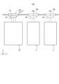
- FIG. 1 is a diagram showing a schematic configuration of an exposure apparatus according to the first embodiment.
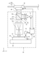
- FIG. 2 is a diagram showing an example of the configuration of an exposure unit according to the first embodiment.
- FIG. 3A shows a view of the spatial light modulator as seen from the -Z direction
- FIG. 3B is a cross-sectional view taken along line AA in FIG. 3A.
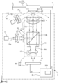
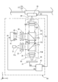
- FIG. 4 is a diagram illustrating an example of the configuration of a first inspection unit according to the first embodiment.
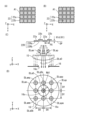
- 5A to 5D are diagrams for roughly explaining the principle of a method for inspecting the state of a spatial light modulator.
- FIG. 6 is a diagram illustrating an example of the configuration of a second inspection unit according to the first embodiment.
- FIG. 1 is a diagram showing a schematic configuration of an exposure apparatus according to the first embodiment.
- FIG. 2 is a diagram showing an example of the configuration of an exposure unit according to the first embodiment.
- FIG. 3A shows a view of the spatial light modulator as seen from the
- FIG. 7A shows a spatial light modulator according to a modified example as viewed from the -Z direction
- FIG. 7B is a cross-sectional view taken along line AA of FIG. 7A.
- FIG. 8 is a diagram showing an example of the configuration of an exposure unit according to the second embodiment.
- FIG. 9 is a diagram illustrating an example of the configuration of a first inspection unit according to the second embodiment.
- FIG. 10 is a diagram showing an example of the configuration of a second inspection unit according to the second embodiment.
- the X, Y, and Z directions indicated by arrows in each figure are mutually orthogonal directions, and the X, Y, and Z directions indicate the same direction in each figure.
- the directions indicated by the arrows are referred to as the +X direction, +Y direction, and +Z direction, respectively.
- the position in the X direction is referred to as the X position
- the position in the Y direction is referred to as the Y position
- the position in the Z direction is referred to as the Z position.
- FIG. 1 is a diagram showing a schematic configuration of an exposure apparatus 100 according to the first embodiment.
- the exposure apparatus 100 includes an exposure section 50, a first inspection section 5, and a second inspection section 6.
- the exposure apparatus 100 also includes a spatial light modulator 20 and a position change mechanism 27.
- the position change mechanism 27 includes a holding portion 28 that holds the spatial light modulator 20, and a guide portion 29.
- the holding portion 28 is movable on the guide portion 29 in the X and Y directions.
- the position change mechanism 27 sets the spatial light modulator 20 to one of the following positions: a first position facing the exposure unit 50, a second position facing the first inspection unit 5, and a third position facing the second inspection unit 6.
- the spatial light modulator 20a shown by the dotted line indicates the spatial light modulator 20 set at the second position
- the spatial light modulator 20b shown by the dotted line indicates the spatial light modulator 20 set at the third position
- the holding portions 28a and 28b shown by the dotted line indicate the positions of the holding portion 28 when holding the spatial light modulators 20a and 20b set at the second and third positions, respectively.
- the positional relationship in which the spatial light modulator 20 faces the exposure unit 50 at the first position is also referred to as the first positional relationship.
- the positional relationship in which the spatial light modulator 20 faces the first inspection unit 5 at the second position is also referred to as the second positional relationship.
- the positional relationship in which the spatial light modulator 20 faces the second inspection unit 6 at the third position is also referred to as the third positional relationship.
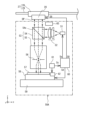
- Fig. 2 is a diagram showing an example of the configuration of the exposure unit 50 according to the first embodiment.
- the exposure unit 50 includes a light sending lens 52, a branching element 54, an imaging optical system 55, a projection aperture stop 56, a substrate stage 58, a surface plate 59, and an exposure control unit 60.
- the exposure unit 50 is a projection exposure unit that projects the light and dark pattern modulated by the spatial light modulator 20 onto an exposed substrate 57, such as a silicon substrate or a glass substrate, on whose surface a photosensitive material is formed.
- the light sending lens 52 and the branching element 54 and the like constitute an illumination optical system IS that uses the exposure illumination light (exposure light) emitted from the exposure light source 51 to illuminate the array surface DP of the spatial light modulator 20.
- the branching element 54, the imaging optical system 55, the projection aperture stop 56 and the like constitute a projection optical system 53 that projects the light from the spatial light modulator 20 onto the exposed substrate 57.
- the exposure illumination light emitted from the exposure light source 51 is shaped by the light sending lens 52, enters a beam splitter or other beam splitter element 54, is reflected by the beam splitting surface 54s of the beam splitter element 14, and is irradiated onto the array surface DP of the spatial light modulator 20.
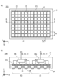
- FIG. 3(A) shows the spatial light modulator 20 as viewed from the -Z direction
- FIG. 3(B) is a cross-sectional view taken along line A-A in FIG. 3(A).
- a plurality of spatial light modulation elements 22 are arranged, each having a reflective surface 22R at its -Z end.
- the spatial light modulation elements 22 are arranged so that each reflective surface 22R roughly coincides with an array surface DP, which is an XY plane near the -Z end of the spatial light modulator 20.
- the spatial light modulation elements 22 are arranged along the X and Y directions, and the spatial light modulation elements 22 are arranged with a period PX in the X direction and a period PY in the Y direction.
- Each of the spatial light modulation elements 22 is held in the housing 21 of the spatial light modulator 20 via an elastic holding member (not shown).
- a counter electrode 23 is disposed on the portion of the housing 21 facing the +Z side of each spatial light modulation element 22.
- each spatial light modulation element 22 moves parallel in the Z direction and is set to a Z position corresponding to the voltage of the control signal Sa applied to the opposing counter electrode 23.
- the modulation control unit 24 sends a control signal Sa to each counter electrode 23 based on a control signal S8 supplied from the exposure control unit 60.
- the Z position of the spatial light modulation element 22 is switched between the on position and the off position by the control signal Sa.
- the size of each spatial light modulation element 22 is too small to be resolved by the projection optical system 53 described later, when all the spatial light modulation elements 22 are in the on position or all are in the off position in an area that can be resolved by the projection optical system 53, the zeroth-order diffracted light of the exposure illumination light from the illumination optical system IS that enters the area enters the projection optical system 53.
- 2 ⁇ 2 spatial light modulation elements 22 may be located in the area that can be resolved by the projection optical system 53.
- the exposure illumination light from the illumination optical system IS enters an area where the spatial light modulation elements 22 in the on position and the spatial light modulation elements 22 in the off position are alternately located, the exposure illumination light is diffracted in this area, the zeroth-order diffracted light of the exposure illumination light almost disappears, and the ⁇ 1st-order or higher diffracted light of the exposure illumination light reaches the non-exposure optical path outside the projection optical system 53.
- the spatial light modulator 20 imparts a pattern to the exposure illumination light by setting each of the multiple spatial light modulation elements 22 to either an on position or an off position.
- the exposure illumination light that has been given a pattern by the spatial light modulator 20 enters the splitting element 54 again, passes through the splitting surface 54s of the splitting element 54, and enters the imaging optical system 55.
- the exposure control unit 60 sends a control signal S8 to the spatial light modulator 20, causing a predetermined amount of displacement to be applied to a predetermined spatial light modulation element 22 in the array surface DP.
- the substrate to be exposed 57 is placed on a substrate stage 58 which is placed on a base plate 59.
- the substrate to be exposed 57 can be moved in the X and Y directions on the base plate 59 by the substrate stage 58.
- the substrate to be exposed 57 can also be moved a small distance in the Z direction by the substrate stage 58, and can be rotated (tilted) a small angle around the X and Y directions as rotation axes.
- the position of the exposed substrate 57 in the X and Y directions is measured by a position measurement unit 61 via the position of a reflector 62 provided on the substrate stage 58, and transmitted as a measurement signal Sc to an exposure control unit 60.
- the exposure control unit 60 sends a position control signal Sd to the substrate stage 58 based on the measurement signal Sc, and controls the exposed substrate 57 to be positioned at a predetermined X and Y position.
- the exposure control unit 60 sends an exposure control signal Se to the exposure light source 51, and controls the emission timing and amount of light emitted by the exposure light source 51.
- the exposure unit 50 may be a scanning type exposure device that performs exposure while scanning the exposed substrate 57 and substrate stage 58 in the XY in-plane direction relative to the projection optical system 53.
- the exposure unit 50 may be a step-and-repeat type exposure device that performs exposure while the exposed substrate 57 and substrate stage 58 are fixed relative to the projection optical system 53, and then moves the exposed substrate 57 and substrate stage 58 sequentially relative to the projection optical system 53 after exposure is complete.
- the wavelength band of the exposure illumination light emitted from the exposure light source 51 is, for example, a wavelength band with a peak wavelength of 450 nm or less.
- the wavelength band of the exposure illumination light may be, for example, a wavelength band with a peak wavelength of 248 nm, or a wavelength band with a peak wavelength of 193 nm.
- the exposure light source 51 may be incorporated inside the exposure section 50, or may be disposed outside the exposure section 50.
- the exposure illumination light may be guided from the exposure light source 51 to the exposure section 50 using a light-guiding member such as an optical fiber.
- the wavelength band of the exposure illumination light may be referred to as the first wavelength band.
- the state of the spatial light modulator 20 is inspected using at least one of the first inspection unit 5 and the second inspection unit 6 before or after the exposure process of the exposed substrate 57 in the exposure unit 50.
- a control signal Sa is input to the spatial light modulators 22, which sets some of the Z positions of the spatial light modulators 22 as a first set position and sets some of the other Z positions of the spatial light modulators 22 as a second set position
- the position change mechanism 27 moves the spatial light modulator 20 from a first position facing the exposure unit 50 to a second position facing the first inspection unit 5 or a third position facing the second inspection unit 6.
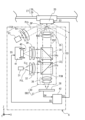
- the first inspection unit 5 is a diagram showing the configuration of the first inspection unit 5 according to the first embodiment.
- the first inspection unit 5 includes a detection light source 11, a light sending lens 12, an illumination aperture stop 13, a branching element 14, an objective lens 15, a detection aperture stop 16, an imaging lens 17, an imaging unit 18, and a first control unit 25.
- the first inspection unit 5 has a detection field of view wider than that of the second inspection unit 6.
- the light sending lens 12, illumination aperture stop 13, branching element 14, objective lens 15, etc. constitute a first illumination system IS1 that irradiates the inspection light ILb onto the array surface DP of the spatial light modulation element 22 that constitutes the spatial light modulator 20.
- the wavelength band of the inspection light ILb is longer than the first wavelength band of the exposure illumination light.
- the wavelength band of the inspection light ILb is, for example, a wavelength band with a peak wavelength of 530 [nm]. In the following explanation, the wavelength band of the inspection light ILb may be referred to as the second wavelength band.
- the objective lens 15, branching element 14, detection aperture stop 16, and imaging lens 17, etc., included in the area surrounded by the two-dot chain line, constitute the first detection optical system 10 that forms an image of the array surface DP on the imaging surface 19 of the imaging unit 18, such as a solid-state imaging element.
- the imaging unit 18 and the first detection optical system 10, etc., constitute the detection device DD1 that detects the inspection light ILb (detection light DLa) reflected by the multiple reflecting surfaces 22R.
- the illumination light ILa emitted from the detection light source 11 is roughly collimated by the light sending lens 12, and its diameter is restricted by the illumination aperture stop 13 to become the inspection light ILb.
- the inspection light ILb then enters a splitting element 14 such as a beam splitter, is reflected by the splitting surface 14s of the splitting element 14, and is then focused by the objective lens 15. It is then irradiated onto the array surface DP of the spatial light modulator 20 as an inspection light beam having a numerical aperture (illumination NA) according to the aperture diameter of the illumination aperture stop 13.
- the inspection light ILb is reflected by a number of reflecting surfaces 22R (see FIG. 2) arranged near the array surface DP, and a part of it becomes detection light DLa and enters the objective lens 15.
- the detection light DLa then enters the branching element 14, passes through the branching surface 14s of the branching element 14, and has its diameter restricted by the detection aperture stop 16 to become detection light DLb.
- the detection light DLb is focused by the imaging lens 17 and enters the imaging surface 19 of the imaging unit 18, forming an image of the array surface DP on the imaging surface 19.
- the image of the array surface DP is detected by the imaging unit 18, i.e., photoelectrically converted into an electrical signal, and transmitted to the first control unit 25 as an image signal S2.
- the amount of light at each part of the image of the array surface DP detected by the imaging pixels that make up the imaging unit 18 is hereinafter also referred to as the "detected amount of light.”
- the detection light source 11 may be, for example, a semiconductor laser or an LED with a relatively narrow emission wavelength range.
- the light-transmitting lens 12, objective lens 15, and imaging lens 17 are not limited to the configuration including the number of lenses shown in the figure (two lenses), but may include any number of lenses, and each may include a reflective optical system.
- the splitting element 14 is not limited to the beam splitter described above, but may be a half mirror made of flat glass or the like.
- the first control unit 25 sends a control signal S1 to the spatial light modulator 20, and controls each spatial light modulation element 22 of the spatial light modulator 20 to be set to a predetermined Z position during inspection.
- the first control unit 25 calculates the position information of each spatial light modulation element 22 of the spatial light modulator 20 based on the image signal S2.
- the first control unit 25 determines the state of the spatial light modulator 20 based on the position information of each spatial light modulation element 22 of the spatial light modulator 20.
- FIGS. 5(A) to 5(D) are diagrams that outline the principles of a method for inspecting the state of the spatial light modulator 20.
- FIG. 5(A) and FIG. 5(B) are diagrams that show examples of the operating states of the spatial light modulation elements 22 arranged in the first region A1 of the spatial light modulator 20 shown in FIG. 3(A), as viewed from the -Z direction.
- the first region A1 is any region on the array surface DP of the spatial light modulator 20.
- the number of spatial light modulation elements 22 included in the first region A1 is not limited to 4 ⁇ 4 as shown in FIG. 3(A) and FIG. 5(A), and may be any other number.
- Figure 5(C) is a cross-sectional view of the spatial light modulator 22 in the first area A1 in the operating state shown in Figure 5(B) and the objective lens 15 shown in Figure 4, viewed from the +Y direction.
- the inspection light ILb (see Figure 4) irradiated to the spatial light modulator 20 from the -Z direction is omitted.
- the reflecting surface 22R of the first group of spatial light modulation elements 22a is marked with the symbol 22Ra
- the reflecting surface 22R of the second group of spatial light modulation elements 22b is marked with the symbol 22Rb.
- the first group of spatial light modulation elements 22a are marked with a diagonal line extending from the upper left to the lower right
- the second group of spatial light modulation elements 22b are marked with a diagonal line extending from the lower left to the upper right to distinguish them from one another.
- the reflective surface 22Ra of the first group of spatial light modulation elements 22a is set to have a first set Z position by a control signal S1 from the first control unit 25 and a control signal Sa from the modulation control unit 24.
- the reflective surface 22Ra of the first group of spatial light modulation elements 22a is set to have a Z position of 0 (on the array surface DP).
- a predetermined first voltage V1 is applied to the opposing electrode 23 based on the control signal S1 from the first control unit 25 and the control signal Sa from the modulation control unit 24.
- the reflecting surface 22Rb of the other spatial light modulation element 22b of the second group is set to a second set position in Z direction away from the array surface DP by a set position difference H1d in the +Z direction by a control signal S1 from the first control unit 25 and a control signal Sa from the modulation control unit 24.
- a predetermined second voltage V2 is applied to the opposing electrode 23 based on the control signal S1 from the first control unit 25 and the control signal Sa from the modulation control unit 24.
- the difference between the set position (first set position) of the Z position of the reflecting surface 22Ra of the spatial light modulator 22a and the set position (second set value) of the Z position of the reflecting surface 22Rb of the spatial light modulator 22b may be referred to as the Z stroke set value.
- the difference between the actual Z position of the reflecting surface 22Ra of the spatial light modulation element 22a of the first group and the actual Z position of the reflecting surface 22Rb of the spatial light modulation element 22b of the second group is called the position difference H1.
- the position difference H1 does not necessarily coincide with the set position difference H1d described above.
- the difference between the actual Z position of the reflecting surface 22Ra of the spatial light modulation element 22a and the actual Z position of the reflecting surface 22Rb of the spatial light modulation element 22b is sometimes called the actual Z stroke.
- the position difference H1 and the above-mentioned set position difference H1d represent the length of the same part because the difference in length is small compared to the scale of the drawing.
- a first group of spatial light modulation elements 22a and a second group of spatial light modulation elements 22b having a position difference H1 between them in the Z direction are arranged alternately based on a control signal S1 from the first control unit 25.
- "alternate arrangement” means that the first group of spatial light modulation elements 22a and the second group of spatial light modulation elements 22b are arranged alternately among the multiple spatial light modulation elements 22 arranged along a predetermined direction in the XY plane.
- FIG. 5(A) shows an operating state in which the first group of spatial light modulation elements 22a and the second group of spatial light modulation elements 22b are arranged alternately along two directions, the X direction and the Y direction, in other words, in a checkered grid pattern (checkered flag pattern).
- FIG. 5(B) shows an operating state in which the first group of spatial light modulation elements 22a and the second group of spatial light modulation elements 22b are arranged alternately along the X direction, and either the first group of spatial light modulation elements 22a or the second group of spatial light modulation elements 22b are arranged consecutively along the Y direction.
- FIG. 5(C) is a diagram showing the reflected light from the spatial light modulation element 22 in the first area A1 in the operating state shown in FIG. 5(B), so the reflected light is separated into specular reflected light DLa0 and diffracted light such as +1st order diffracted light DLap and -1st order diffracted light DLam in the X direction.
- the specularly reflected light DLa0 is emitted in a direction perpendicular to the array surface DP (-Z direction).
- FIG. 5(D) is a diagram showing the positions of the specularly reflected light DLa0, the +1st order diffracted light DLap, and the -1st order diffracted light DLam at the detection aperture stop 16.
- the detection aperture stop 16 has an opening 16o with a radius corresponding to the numerical aperture NA1 on the spatial light modulator 20 side of the first detection optical system 10, centered on its center 16c, and the area outside the opening 16o is a shielding section that blocks light.
- FIG. 5(D) also shows the diffracted light generated from the spatial light modulation element 22 in which the first group of spatial light modulation elements 22a and the second group of spatial light modulation elements 22b, which are different in Z position as shown in FIG. 5(A), are arranged in a checkerboard pattern. From the spatial light modulation element 22 shown in FIG.
- the (X-side order, Y-side order) respectively generates (0th order, +1st order) diffracted light DLa0p, (0th order, -1st order) diffracted light DLap, (-1st order, 0th order) diffracted light DLam, (+1st order, +1st order) diffracted light DLapp, (+1st order, -1st order) diffracted light DLapm, (-1st order, +1st order) diffracted light DLamp, and (-1st order, -1st order) diffracted light DLamm.
- Regular reflection light DLa0 is also generated.
- the first-order diffracted light (DLa0p, DLa0m, DLap, DLam, DLapp, DLapm, DLamp, DLamm) from the spatial light modulator 20 is blocked by the detection aperture stop 16 and does not reach the imaging unit 18.
- the specularly reflected light DLa0 from the spatial light modulator 20 passes through the opening 16o of the detection aperture stop 16, passes through the imaging lens 17, and reaches the imaging unit 18. Then, an image of the array surface DP is formed on the imaging surface 19 of the imaging unit 18. Therefore, the amount of specularly reflected light DLa0 from each region on the array surface DP, such as the first region A1, is detected by each imaging pixel included in the imaging unit 18 as a detected light amount, which is the amount of light of the image of each region on the array surface DP.
- the amount (intensity) of specularly reflected light DLa0 when illumination light of a specified wavelength is irradiated onto the array surface DP with a specified amount (intensity) of light is determined according to the position difference H1, which is the difference between the actual Z position of the first group of spatial light modulation elements 22a and the actual Z position of the second group of spatial light modulation elements 22b.
- the position difference H1 between the first group of spatial light modulation elements 22a and the second group of spatial light modulation elements 22b in the first region A1 or other region can be calculated from the intensity of the specularly reflected light DLa0, i.e., the detected light amount of the image of the first region A1 or other region.
- the first control unit 25 calculates the position difference H1 between the first group of spatial light modulation elements 22a and the second group of spatial light modulation elements 22b in an area such as the first area A1 of the spatial light modulator 20 based on the image signal S2 detected by the imaging unit 18 and the correspondence between the detected light amount and the position difference H1.
- the correspondence between the detected light amount and the position difference H1 may be stored in a memory unit 25M such as a solid-state memory or a magnetic memory.
- the first control unit 25 stores the calculated position difference H1 in the memory unit 25M.
- the position of the spatial light modulator 20 is changed by the position changing mechanism 27, and, for example, the second area A2 is inspected.
- the above-described inspection (obtaining the Z-direction position information of the spatial light modulation element 22) is performed on multiple areas within the spatial light modulator 20, and the state of the spatial light modulator 20 is determined. For example, it is determined whether the spatial light modulation element 22 of the spatial light modulator 20 can be driven with the set position difference H1d.
- the first inspection unit 5 may employ, for example, the inspection method described in International Publication No. WO 2022/038683.
- the spatial light modulation element 22 is illuminated with the exposure illumination light, and its Z-direction position is changed based on the control signal Sa. At this time, each spatial light modulation element 22 is charged by the exposure illumination light. Therefore, the voltage of the control signal Sa for setting the Z position of the spatial light modulation element 22 to the set position is determined taking into consideration the charging of the spatial light modulation element 22 by the exposure illumination light.
- the inventors have found that when, after exposure in the exposure unit 50, the spatial light modulator 20 is moved to the second position by the position change mechanism 27 and the state of the spatial light modulator 20 is inspected by the first inspection unit 5, the charge on the spatial light modulator 22 accumulated by the exposure illumination light is lost while the spatial light modulator 20 is moving or being inspected, and the Z-direction position of the spatial light modulator 22 cannot be maintained by the voltage based on the control signal Sa applied to each opposing electrode 23 alone, and the Z-direction position of the spatial light modulator 22 may change during inspection or the spatial light modulator 22 may become stuck.
- the first inspection unit 5 therefore includes a second illumination system IS2 that irradiates the entire array surface DP of the spatial light modulator 20 with light (protection light PLa) different from the inspection light ILb while inspecting the spatial light modulator 20.
- a second illumination system IS2 that irradiates the entire array surface DP of the spatial light modulator 20 with light (protection light PLa) different from the inspection light ILb while inspecting the spatial light modulator 20.
- the second illumination system IS2 includes a light source 81 and a light-transmitting lens 82.
- the light source 81 emits protective light PLa that is separate from the inspection light ILb.
- the protective light PLa emitted from the light source 81 is approximately collimated by the light-transmitting lens 82 and illuminates the entire array surface DP of the spatial light modulator 20.
- the protective light PLa is incident on the array surface DP from an oblique direction. This prevents the protective light PLa from entering the detection device DD1.
- the timing to start irradiating the protective light PLa may be, for example, the timing when the spatial light modulator 20 is placed at the second position, the timing when the spatial light modulator 20 is moved to a position different from the first position, or the timing when inspection of the spatial light modulator 20 starts, as long as the protective light PLa can be irradiated to the spatial light modulator 20 while inspecting the spatial light modulator 20, in other words, as long as the protective light PLa can be irradiated to the spatial light modulator 20 array surface DP while changing the voltage applied to each of the opposing electrodes 23 that face the multiple spatial light modulation elements 22.
- the wavelength band of the curing light PLa is, for example, a wavelength band with a peak wavelength of 450 [nm] or less.
- the wavelength band of the curing light PLa may be, for example, a wavelength band with a peak wavelength of 248 [nm] or a wavelength band with a peak wavelength of 193 [nm].
- the wavelength band of the curing light PLa does not have to match the first wavelength band of the exposure illumination light as long as it is shorter than the second wavelength band of the inspection light ILb, or closer to the first wavelength band of the exposure illumination light than the second wavelength band.
- the wavelength band of the curing light PLa may be referred to as the third wavelength band.
- the third wavelength band at least partially overlaps with the first wavelength band of the exposure illumination light, and it is more preferable that the third wavelength band of the curing light PLa and the first wavelength band of the exposure illumination light match.
- the spatial light modulator 22 is irradiated with the protective light PLa, the charge on the spatial light modulator 22 is prevented from escaping, and the charged state of the spatial light modulator 22 during the inspection period can be made substantially the same as the charged state of the spatial light modulator 22 during the exposure period. This makes it possible to prevent the Z position of the spatial light modulator 22 from changing during the inspection period and to prevent the spatial light modulator 22 from sticking.
- the inspection can be performed in a state similar to the state in which the spatial light modulator 20 is used in the exposure section 50, the inspection accuracy can be improved.
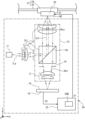
- FIG. 6 is a diagram showing an example of the configuration of the second inspection unit 6 according to the first embodiment.
- the second inspection unit 6 includes a detection light source 31, a light sending lens 32, a first branching element 33, a second branching element 34, an objective lens 35, an imaging lens 36, a reference lens 39, a reference reflecting surface 40, a movable support unit 41, an imaging unit 37, and a second control unit 42 within an area surrounded by a dashed line in Fig. 6.
- the light sending lens 32, the first branching element 33, the second branching element 34, and the objective lens 35 constitute a third illumination system IS3 that irradiates the inspection light onto the array surface DP of the spatial light modulation element 22 that constitutes the spatial light modulator 20.
- the objective lens 35, second branching element 34, first branching element 33, and imaging lens 36, etc., included in the area surrounded by the two-dot chain line in Figure 6, constitute the second detection optical system 30 that forms an image of the array surface DP on the imaging surface 38 of the imaging unit 37, such as a solid-state imaging element.
- the imaging unit 37 and the second detection optical system 30, etc., constitute the detection device DD2 that detects the inspection light reflected by the reflecting surface 22R.
- the inspection light ILc emitted from the detection light source 31 passes through the illumination light path PIL, is approximately collimated by the light sending lens 32, enters the first splitter element 33, is reflected by the splitting surface 33s of the first splitter element 33, and then enters the second splitter element 34.
- the inspection light is then amplitude-split by the splitting surface 34s of the second splitter element 34 into detection light, which is light that passes through the splitting surface 34s and passes through the detection light path PDT, and reference light, which is light that is reflected by the splitting surface 34s and passes through the reference light path PRF.
- the wavelength band of the inspection light ILc is longer than the first wavelength band, for example, a wavelength band with a peak wavelength of 530 [nm].
- the wavelength band of the inspection light ILc may be referred to as the fourth wavelength band.
- the detection light passing through the detection optical path PDT is focused by the objective lens 35 and irradiated onto the array surface DP of the spatial light modulator 20.
- the detection light is then reflected by the array surface DP, passes through the objective lens 35 and the detection optical path PDT again, and reaches the second splitter element 34.
- the reference light passing through the reference optical path PRF is focused by the reference lens 39 and irradiated onto the reference reflecting surface 40.
- the reference light is then reflected by the reference reflecting surface 40, passes through the reference lens 39 and the reference optical path PRF again, and reaches the second splitting element 34.
- the detection light that has passed through the splitting surface 34s of the second splitting element 34 and the reference light that has been reflected by the splitting surface 34s of the second splitting element 34 are combined into one light, which passes through the imaging optical path PIM, is focused by the imaging lens 36, and is incident on the imaging surface 38 of the imaging unit 37.
- the second branching element 34 constitutes a so-called interference microscope unit. Therefore, when the optical path length difference between the detection optical path PDT and the reference optical path PRF is equal to or less than the coherence length of the inspection light ILb emitted from the detection light source 31, an image (interference image) formed by the amplitude interference between the image of the array surface DP and the image of the reference reflecting surface 40 is formed on the imaging surface 38.
- the interference image between the array surface DP and the reference reflecting surface 40 is detected by the imaging section 37, i.e., photoelectrically converted and converted into an electrical signal, and transmitted to the second control section 42 as an image signal S4.
- the position (X position) of the reference reflecting surface 40 along the ⁇ X direction which is the traveling direction of the reference light path PRF, can be moved by a movable support part 41 that holds the reference reflecting surface 40.
- a control signal S5 is sent to the movable support part 41, and the image signal S4 detected by the imaging part 37 is signal-processed while changing the X position of the reference reflecting surface 40.
- the second control part 42 sends a control signal S5 to the movable support part 41, and the image signal S4 detected by the imaging part 37 is signal-processed while changing the X position of the reference reflecting surface 40.
- the second control unit 42 measures the Z position of one of the reflecting surfaces 22R of one of the spatial light modulators 22 arranged on the array plane DP based on the change in intensity of the interference image between the image of the reflecting surface 22R and the image of the reference reflecting surface 40, and based on the X position of the reference reflecting surface 40. This allows the state of the spatial light modulator 20 to be inspected.
- the optical path length of the detection optical path PDT may be changed by moving the entire second inspection part 6 in the Z direction.
- a conjugate plane with respect to the array plane DP may be formed within the second detection optical system 30, and a Nipkow disk (Nipkow filter) may be placed on the conjugate plane, causing the second detection optical system 30 to function as a position measurement part.
- the second inspection unit 6 may be set to have a high resolution in order to individually measure the Z position of the reflecting surface 22R of one spatial light modulation element 22. For this reason, the numerical aperture NA2 on the spatial light modulator 20 side of the second detection optical system 30 may be set to be larger than the numerical aperture NA1 on the spatial light modulator 20 side of the first detection optical system 10 of the first inspection unit 5.
- the detection light source 31 may be an LED, for example. Also, in the case of a configuration using the Nipkow disk described above, the detection light source 31 may be a laser light source.
- the light sending lens 32, the objective lens 35, and the imaging lens 36 are not limited to a configuration including the number of lenses (two) shown in the figure, but may include any number of lenses, and each may include a reflective optical system.
- the first branching element 33 and the second branching element 34 are configured by a beam splitter or a half mirror made of flat glass, etc., like the branching element 14 of the first embodiment described above.
- the second control unit 42 Prior to the inspection, the second control unit 42 sends a control signal S3 to the spatial light modulator 20 to set the Z position of the reflecting surface 22R of the spatial light modulation element 22, the Z position of which is to be measured, to a specified position.
- the second inspection unit 6 including the second control unit 42 can detect the difference between the set position of the reflecting surface 22R of the spatial light modulation element 22 and the measured actual Z position of the reflecting surface 22R, i.e., the actual Z position of the reflecting surface 22R, as the detection result.
- the second inspection unit 6, which includes the second control unit 42, may use the control signal S3 to set a predetermined reflecting surface 22R to a number of different set positions and detect the Z position of the reflecting surface 22R at each of these positions.
- the second inspection unit 6 may detect the actual Z position of the reflecting surface 22R over the entire range of the spatial light modulation element 22, or may detect the actual Z position for only a portion of the spatial light modulation element 22.
- the second inspection unit 6 includes a fourth illumination system IS4 that irradiates the entire array surface DP of the spatial light modulator 20 with light (protection light) PLb other than the inspection light ILc while inspecting the spatial light modulator 20.
- the fourth illumination system IS4 includes a light source 91 and a light-transmitting lens 92.
- the light source 91 emits curing light PLb.
- the curing light PLb emitted from the light source 91 is approximately parallelized by the light-transmitting lens 92 and irradiated onto the array surface DP of the spatial light modulator 20.
- the curing light PLb is incident on the array surface DP from an oblique direction.
- the timing for starting irradiation of the protective light PLb may be, for example, the timing when the spatial light modulator 20 is placed in the third position, or the timing when inspection of the spatial light modulator 20 begins.
- the wavelength band of the curing light PLb is, for example, a wavelength band with a peak wavelength of 450 [nm] or less.
- the wavelength band of the curing light PLb may be, for example, a wavelength band with a peak wavelength of 248 [nm] or a wavelength band with a peak wavelength of 193 [nm].
- the wavelength band of the curing light PLb does not have to match the first wavelength band of the exposure illumination light as long as it is shorter than the fourth wavelength band of the inspection light ILc.
- the wavelength band of the curing light PLb at least partially overlaps with the first wavelength band of the exposure illumination light, and it is more preferable that the wavelength band of the curing light PLb and the first wavelength band of the exposure illumination light match.
- the wavelength band of the curing light PLb may be described as the fifth wavelength band.
- the spatial light modulator 22 is irradiated with the protective light PLb, the charge on the spatial light modulator 22 is prevented from escaping, and the charged state of the spatial light modulator 22 during the inspection period can be made the same as the charged state of the spatial light modulator 22 during the exposure process. This makes it possible to prevent the Z position of the spatial light modulator 22 from changing during the inspection period and to prevent the spatial light modulator 22 from sticking.
- the inspection can be performed in a state similar to the state in which the spatial light modulator 20 is used in the exposure section 50, the inspection accuracy can be improved.
- the first inspection unit 5 inspects a spatial light modulator 20 including a plurality of spatial light modulation elements 22 having a reflective surface 22R that reflects exposure illumination light in a first wavelength band.
- the first inspection unit 5 includes a first illumination system IS1 that irradiates an array surface DP on which the reflective surfaces 22R of the plurality of spatial light modulation elements 22 are arranged with inspection light ILb in a second wavelength band longer than the first wavelength band, a second illumination system IS2 that irradiates the array surface DP with protective light PLa in a third wavelength band shorter than the second wavelength band, a detection device DD1 that detects detection light DLa reflected by the plurality of reflective surfaces 22R, and a first control unit 25 that determines the state of the plurality of spatial light modulation elements 22 based on the output of the detection device DD1.
- the second inspection unit 6 also inspects the spatial light modulator 20, which includes a plurality of spatial light modulation elements 22 having a reflective surface 22R that reflects the exposure illumination light of the first wavelength band.
- the second inspection unit 6 includes a third illumination system IS3 that irradiates an array surface DP on which the reflective surfaces 22R of the plurality of spatial light modulation elements 22 are arranged with inspection light ILb of a fourth wavelength band that is longer than the first wavelength band, a fourth illumination system IS4 that irradiates the array surface DP with protective light PLb of a fifth wavelength band that is shorter than the fourth wavelength band of the inspection light ILb, a detection device DD2 that detects the detection light DLa reflected by the plurality of reflective surfaces 22R, and a second control unit 42 that determines the state of the plurality of spatial light modulation elements 22 based on the output of the detection device DD1.
- the charged state of the multiple spatial light modulation elements 22 during the exposure period to be substantially the same as the charged state of the multiple spatial light modulation elements 22 during the inspection period, thereby preventing the charge on the spatial light modulation elements 22 from being lost during the inspection period, causing the position of the spatial light modulation elements 22 in the Z direction to change, or preventing the spatial light modulation elements 22 from sticking.
- the spatial light modulator 20 is used in an exposure apparatus 100 that exposes an exposed substrate 57 with exposure illumination light from the spatial light modulator 20 via the projection optical system 53, and the exposure apparatus 100 is provided with a position change mechanism 27 that changes the relationship between a first position in which the projection optical system 53 and the spatial light modulator 20 face each other and a second position in which the first inspection unit 5 and the spatial light modulator 20 face each other, and the second illumination system IS2 irradiates the spatial light modulator 20 with protective light PLa of the third wavelength band when the first inspection unit 5 and the spatial light modulator 20 are in the second position.
- the spatial light modulator 20 can be moved by the position change mechanism 27 to perform an inspection.
- the Z positions of all spatial light modulation elements 22 included in the spatial light modulator 20 are controlled by one modulation control unit 24.
- the Z positions of the spatial light modulation elements 22 included in the spatial light modulator 20 may be controlled by multiple modulation control units.
- FIG. 7(A) shows a spatial light modulator 20A according to a modified example as viewed from the -Z direction
- FIG. 7(B) is a cross-sectional view taken along line A-A in FIG. 7(A).
- the spatial light modulator 20A includes a first modulation control unit 24a and a second modulation control unit 24b.
- the first modulation control unit 24a controls the Z position of the spatial light modulation element 22 included in the first portion P1 surrounded by a dashed line in FIG. 7, and the second modulation control unit 24b controls the Z position of the reflecting surface 22R of the spatial light modulation element 22 included in the second portion P2.
- the spatial light modulator 20A configured in this manner is inspected by the first inspection unit 5, while inspecting the spatial light modulation element 22 included in the first portion P1, it is sufficient to irradiate the protective light PLa onto at least the first portion P1, and while inspecting the spatial light modulation element 22 included in the second portion P2, it is sufficient to irradiate the protective light PLb onto at least the second portion P2.
- the second inspection unit 6 The same is true for the second inspection unit 6.
- the exposure apparatus 100 has the first inspection unit 5 and the second inspection unit 6, but it may have only one of the first inspection unit 5 and the second inspection unit 6. In other words, it may be possible to omit one of the first inspection unit 5 and the second inspection unit 6.
- the voltage value applied to the opposing electrode 23 may be adjusted to achieve the set position difference H1d based on the inspection results of the first inspection unit 5 and the second inspection unit 6.
- the inspection light ILb, ILc is incident on the array surface DP approximately perpendicularly, and the protection light PLa, PLb is incident on the array surface DP obliquely, but this is not limited to the above.
- the inspection light ILb, ILc may be incident on the array surface DP obliquely, and the protection light PLa, PLb may be incident on the array surface DP approximately perpendicularly.
- the illumination optical system that irradiates the inspection light ILb, ILc onto the array surface DP, the position of the illumination optical system that irradiates the protection light PLa, PLb onto the array surface DP, and the position of the detection optical system may be set appropriately.
- the inspection light ILb, ILc and the protective light PLa, PLb may all be incident approximately perpendicularly to the array surface DP.
- a light combining element such as a dichroic mirror that transmits light in the wavelength band of the inspection light ILb and reflects light in the wavelength band of the protective light PLa may be disposed between the branching element 14 and the objective lens 15, and the combined light of the inspection light ILb and the protective light PLa may be irradiated onto the array surface DP.
- the first inspection unit 5 and the second inspection unit 6 inspect the spatial light modulator 20 having a plurality of spatial light modulation elements 22 that can move in the Z direction.
- the object of inspection by the first inspection unit 5 and the second inspection unit 6 may be an angle modulation type spatial light modulator that has a plurality of spatial light modulation elements that can each rotate within a predetermined angle range.
- a protective light other than the inspection light is irradiated onto the array surface DP of the spatial light modulation elements 22 during the inspection period.
- the charging state of the spatial light modulation elements 22 during the inspection period and during the exposure process is made substantially the same by removing the charging of the spatial light modulation elements 22 caused by the exposure illumination light.
- FIG. 8 is a diagram showing an example of the configuration of an exposure unit 50A according to the second embodiment.
- the exposure unit 50A according to the second embodiment differs from the exposure unit 50 according to the first embodiment in that it has an ionizer 65.
- the ionizer 65 generates positive or negative ions.
- the ions generated by the ionizer 65 neutralize (de-electrify) the charge on the spatial light modulation element 22.
- the rest of the configuration is the same as that of the exposure unit 50 according to the first embodiment, so a detailed description will be omitted.
- FIG. 9 is a diagram showing an example of the configuration of the first inspection unit 5A according to the second embodiment.
- the first inspection unit 5A according to the second embodiment differs from the first inspection unit 5 according to the first embodiment in that it does not have the second illumination system IS2.
- the charge on the spatial light modulation element 22 is discharged by the ionizer 65 in the exposure unit 50A, so that the charged state of the spatial light modulation element 22 of the spatial light modulator 20 during exposure and the charged state of the spatial light modulation element 22 of the spatial light modulator 20 during inspection can be made substantially the same, even if the first inspection unit 5A does not irradiate the spatial light modulator 20 with exposure illumination light.
- the other configurations are the same as those of the first inspection unit 5 according to the first embodiment, so detailed explanations are omitted.
- FIG. 10 is a diagram showing an example of the configuration of the second inspection section 6A according to the second embodiment.
- the second inspection section 6A according to the second embodiment differs from the second inspection section 6 according to the first embodiment in that it does not have a fourth illumination system IS4.
- the charge on the spatial light modulation element 22 is discharged by the ionizer 65 in the exposure section 50A, so that the charged state of the spatial light modulation element 22 of the spatial light modulator 20 during exposure and the charged state of the spatial light modulation element 22 of the spatial light modulator 20 during inspection can be made substantially the same, even if the second inspection section 6A does not irradiate the spatial light modulator 20 with exposure illumination light.
- the other configurations are the same as those of the second inspection section 6 according to the first embodiment, so detailed explanations are omitted.
- an ionizer 65 is provided in the exposure unit 50A to remove the charge on the spatial light modulation element 22. This makes it possible to make the charged state of the spatial light modulation element 22 of the spatial light modulator 20 during exposure substantially the same as the charged state of the spatial light modulation element 22 of the spatial light modulator 20 during inspection, thereby making it possible to prevent the position of the spatial light modulation element 22 in the Z direction from changing during the inspection period and to prevent the spatial light modulation element 22 from sticking.
- the first and second inspection units are included in the exposure device, but this is not limited to the above.
- An inspection device including at least one of the first and second inspection units may be provided separately from the exposure device, and the state of the spatial light modulator 20 may be inspected in the inspection device.
- An inspection apparatus for inspecting a spatial light modulator including a plurality of spatial light modulation elements each having a reflective surface that reflects light in a first wavelength band comprising: a first illumination system that irradiates an arrangement surface on which the reflection surfaces of the plurality of spatial light modulation elements are arranged with inspection light of a second wavelength band different from the first wavelength band; a second illumination system that irradiates the array surface with light of a third wavelength band that is closer to the first wavelength band than the second wavelength band; a detection device that detects the inspection light reflected by the plurality of reflecting surfaces; a determination unit that determines a state of the plurality of spatial light modulation elements based on an output of the detection device; An inspection device comprising: [Appendix 2] 1.
- a method for inspecting a spatial light modulator including a plurality of spatial light modulation elements each having a reflective surface that reflects light in a first wavelength band comprising: Irradiating an array surface on which the reflection surfaces of each of the plurality of spatial light modulation elements are arranged with inspection light of a second wavelength band different from the first wavelength band; irradiating the array surface with light of a third wavelength band that is closer to the first wavelength band than the second wavelength band; detecting the inspection light reflected by the plurality of reflective surfaces; determining states of the plurality of spatial light modulation elements based on a detection result from the detecting;
- the inspection method includes: [Appendix 3] 1.
- a method for inspecting a spatial light modulator including a plurality of spatial light modulation elements each having a reflective surface that reflects light in a first wavelength band comprising: Irradiating an array surface on which the reflection surfaces of each of the plurality of spatial light modulation elements are arranged with inspection light of a second wavelength band different from the first wavelength band; irradiating the array surface with light of a third wavelength band closer to the first wavelength band than the second wavelength band while changing a voltage applied to each of a plurality of counter electrodes facing the plurality of spatial light modulation elements, respectively; detecting light reflected from a plurality of said reflective surfaces; determining states of the plurality of spatial light modulation elements based on a detection result from the detecting;
- the inspection method includes: [Appendix 4] An inspection apparatus for inspecting a spatial light modulator including a plurality of spatial light modulation elements each having a reflective surface, comprising: a first illumination system that irradiates an inspection light onto an arrangement surface on which the reflection surfaces of the plurality
- a method for inspecting a spatial light modulator including a plurality of spatial light modulation elements each having a reflective surface comprising the steps of: Irradiating an array surface on which the reflection surfaces of the plurality of spatial light modulation elements are arranged with an inspection light; Illuminating the array surface with light different from the inspection light from a direction different from the inspection light; forming an image of the array surface based on light from a plurality of the reflecting surfaces; Detecting the formed image of the array surface; determining states of the plurality of spatial light modulation elements based on a detected light amount that is a light amount of the detected image;
- the inspection method includes: [Appendix 6] 1.
- a method for inspecting a spatial light modulator including a plurality of spatial light modulation elements each having a reflective surface comprising the steps of: Irradiating an array surface on which the reflection surfaces of the plurality of spatial light modulation elements are arranged with an inspection light; irradiating the array surface with light different from the inspection light from a direction different from that of the inspection light while changing a voltage applied to each of a plurality of counter electrodes that face the plurality of spatial light modulation elements, respectively; forming an image of the array surface based on light from a plurality of the reflecting surfaces; Detecting the formed image of the array surface; determining states of the plurality of spatial light modulation elements based on a detected light amount that is a light amount of the detected image;
- the inspection method includes:
- Second inspection section 20 Spatial light modulator 22 Spatial light modulation element 22R Reflection surface 24a First modulation control section 24b Second modulation control section 25 First control section 27 Position change mechanism 42 Second control section 50, 50A Exposure section 57 Exposed substrate 100 Exposure device DD1 Detection device DD2 Detection device DP Array surface IS1 First illumination system IS2 Second illumination system IS3 Third illumination system IS4 Fourth illumination system
Landscapes
- Physics & Mathematics (AREA)
- General Physics & Mathematics (AREA)
- Optics & Photonics (AREA)
- Chemical & Material Sciences (AREA)
- Analytical Chemistry (AREA)
- Exposure Of Semiconductors, Excluding Electron Or Ion Beam Exposure (AREA)
Abstract
検査装置は、第1波長帯域の光を反射する反射面を有する複数の空間光変調素子を備える空間光変調器を検査する検査装置であって、前記複数の空間光変調素子の各々の前記反射面が配列される配列面に前記第1波長帯域よりも長波長側の第2波長帯域の検査光を照射する第1照明系と、前記第2波長帯域よりも短波長側の第3波長帯域の光を前記配列面に照射する第2照明系と、複数の前記反射面で反射された前記検査光を検出する検出装置と、前記検出装置の出力に基づいて、前記複数の空間光変調素子の状態を決定する決定部と、を備える。
Description
検査装置、露光装置、検査方法、及びデバイス製造方法に関する。
露光転写すべきパターンを形成する部材として、照射光の所定方向への反射率を可変とするデジタルミラーデバイス等の空間光変調器を用いる露光装置が提案されている(特許文献1)。
第1の開示の態様によれば、検査装置は、第1波長帯域の光を反射する反射面を有する複数の空間光変調素子を備える空間光変調器を検査する検査装置であって、前記複数の空間光変調素子の各々の前記反射面が配列される配列面に前記第1波長帯域よりも長波長側の第2波長帯域の検査光を照射する第1照明系と、前記第2波長帯域よりも短波長側の第3波長帯域の光を前記配列面に照射する第2照明系と、複数の前記反射面で反射された前記検査光を検出する検出装置と、前記検出装置の出力に基づいて、前記複数の空間光変調素子の状態を決定する決定部と、を備える。
第2の開示の態様によれば、露光装置は、投影光学系を介した空間光変調器からの露光光で被露光基板を露光する露光装置であって、検査光を前記空間光変調器に照射する第1照明系と、前記空間光変調器の複数の反射面で反射された前記検査光を検出する検出装置と、を備える検査装置と、前記投影光学系と前記空間光変調器とが対向する第1位置関係と、前記検出装置と前記空間光変調器とが対向する第2位置関係との一方にする位置変更機構と、前記第1位置関係とは異なる位置関係であるときに前記空間光変調器に前記露光光又は前記露光光と同波長の光を前記空間光変調器に照射する第2照明系と、を備える。
第3の開示の態様によれば、露光装置は、投影光学系を介した空間光変調器からの露光光で被露光基板を露光する露光装置であって、検査光を前記空間光変調器に照射する検査照明系と、前記空間光変調器の複数の反射面で反射された前記検査光を検出する検出装置と、を備える検査装置と、前記投影光学系と前記空間光変調器とが対向する第1位置関係と、前記検出装置と前記空間光変調器とが対向する第2位置関係との一方にする位置変更機構と、前記投影光学系と前記空間光変調器とが前記第1位置関係であるときに前記空間光変調器を除電する除電装置と、を備える。
第4の開示の態様によれば、検査方法は、第1波長帯域の光を反射する反射面を有する複数の空間光変調素子を備える空間光変調器の検査方法であって、前記複数の空間光変調素子の各々の前記反射面が配列される配列面に前記第1波長帯域よりも長波長側の第2波長帯域の検査光を照射することと、前記第2波長帯域よりも短波長側の第3波長帯域の光を前記配列面に照射することと、複数の前記反射面で反射された前記検査光を検出することと、前記検出することによる検出結果に基づいて、前記複数の空間光変調素子の状態を決定することと、を含む。
第5の開示の態様によれば、検査方法は、第1波長帯域の光を反射する反射面を有する複数の空間光変調素子を備える空間光変調器の検査方法であって、前記複数の空間光変調素子の各々の前記反射面が配列される配列面に前記第1波長帯域よりも長波長側の第2波長帯域の検査光を照射することと、前記複数の空間光変調素子とそれぞれ対向する複数の対向電極の各々に印加する電圧を変化させている間、前記第2波長帯域よりも短波長側の第3波長帯域の光を前記配列面に照射することと、複数の前記反射面で反射された光を検出することと、前記検出することによる検出結果に基づいて、前記複数の空間光変調素子の状態を決定することと、を含む。
第6の開示の態様によれば、露光装置は、上記検査装置と、前記空間光変調器を露光光で照明する第3照明系と、前記空間光変調器からの前記露光光を被露光基板に投影する投影光学系と、を備える。
第7の開示の態様によれば、デバイス製造方法は、基板の表面上にレジストを形成することと、上記露光装置を用いて露光パターンを露光することと、前記露光パターンに基づいて回路パターンを形成することと、を含む。
なお、後述の実施形態の構成を適宜改良しても良く、また、少なくとも一部を他の構成物に代替させても良い。更に、その配置について特に限定のない構成要件は、実施形態で開示した配置に限らず、その機能を達成できる位置に配置することができる。
《第1実施形態》
以下、第1実施形態に係る露光装置100について、図1~図6に基づいて説明する。なお、各図に矢印で示したX方向、Y方向およびZ方向はそれぞれ直交する方向であるとともに、X方向、Y方向およびZ方向のそれぞれは各図において同一の方向を示している。以下では、各矢印の示す方向を、それぞれ+X方向、+Y方向および+Z方向と呼ぶ。また、X方向の位置をX位置、Y方向の位置をY位置、Z方向の位置をZ位置と呼ぶ。
以下、第1実施形態に係る露光装置100について、図1~図6に基づいて説明する。なお、各図に矢印で示したX方向、Y方向およびZ方向はそれぞれ直交する方向であるとともに、X方向、Y方向およびZ方向のそれぞれは各図において同一の方向を示している。以下では、各矢印の示す方向を、それぞれ+X方向、+Y方向および+Z方向と呼ぶ。また、X方向の位置をX位置、Y方向の位置をY位置、Z方向の位置をZ位置と呼ぶ。
図1は、第1実施形態に係る露光装置100の概略構成を示す図である。露光装置100は、露光部50と、第1検査部5と、第2検査部6と、を備える。また、露光装置100は、空間光変調器20と、位置変更機構27と、を備える。
位置変更機構27は、空間光変調器20を保持する保持部28と、ガイド部29と、を備える。保持部28はガイド部29上を、X方向およびY方向に移動可能となっている。
位置変更機構27は空間光変調器20を、露光部50と対向する第1位置と、第1検査部5と対向する第2位置と、第2検査部6と対向する第3位置と、のいずれか1つの位置に設定する。
図1において点線で示した空間光変調器20aは、第2位置に設定された空間光変調器20を示しており、同じく点線で示した空間光変調器20bは、第3位置に設定された空間光変調器20を示している。また、点線で示した保持部28a、28bは、それぞれ第2位置および第3位置に設定された空間光変調器20a,20bを保持する際の保持部28の位置を表している。
空間光変調器20が第1位置において露光部50と対向する位置関係を第1位置関係ともいう。空間光変調器20が第2位置において第1検査部5と対向する位置関係を第2位置関係ともいう。また、空間光変調器20が第3位置において第2検査部6と対向する位置関係を第3位置関係ともいう。
(露光部50)
図2は、第1実施形態に係る露光部50の構成の一例を示す図である。図2に示すように、露光部50は、送光レンズ52、分岐素子54、結像光学系55、投影開口絞り56、基板ステージ58、定盤59、および露光制御部60等を備えている。
図2は、第1実施形態に係る露光部50の構成の一例を示す図である。図2に示すように、露光部50は、送光レンズ52、分岐素子54、結像光学系55、投影開口絞り56、基板ステージ58、定盤59、および露光制御部60等を備えている。
露光部50は、空間光変調器20により変調された光の明暗パターンを、表面に感光物質が形成されたシリコン基板またはガラス基板等の被露光基板57上に投影する投影露光部である。
送光レンズ52および分岐素子54等により、露光光源51から射出される露光用照明光(露光光)を用いて、空間光変調器20の配列面DPを照明する照明光学系ISが構成されている。分岐素子54、結像光学系55、及び投影開口絞り56等により、空間光変調器20からの光を被露光基板57に投影する投影光学系53が構成されている。
露光光源51から射出される露光用照明光は、送光レンズ52により整形され、ビームスプリッタ等の分岐素子54に入射し、分岐素子14の分岐面54sで反射されて空間光変調器20の配列面DPに照射される。
図3(A)は空間光変調器20を-Z方向から見た図を示し、図3(B)は、図3(A)におけるA-A線断面図である。
空間光変調器20の-Z側の面には、それぞれの-Z側の端部に反射面22Rを有する複数の空間光変調素子22が配置されている。複数の空間光変調素子22は、それぞれの反射面22Rが、空間光変調器20の-Z側の端部の近傍の1つのXY平面である配列面DPと概ね一致するように配置されている。一例として、複数の空間光変調素子22は、X方向、およびY方向に沿って配置されており、空間光変調素子22のX方向の配置の周期はPX、Y方向の配置の周期はPYである。
空間光変調素子22のそれぞれは、弾性を有する不図示の保持部材を介して、空間光変調器20の筐体21に保持されている。筐体21の、各空間光変調素子22の+Z側に対向する部分には、対向電極23がそれぞれ配置されている。変調制御部24からそれぞれ対向電極23に対して制御信号Saとして所定の電圧が印加されると、各空間光変調素子22はZ方向に平行移動して、対向する対向電極23に印加された制御信号Saの電圧に応じたZ位置に設定される。変調制御部24は、露光制御部60から供給される制御信号S8に基づいて、各対向電極23に制御信号Saを送る。
制御信号Saにより、空間光変調素子22のZ位置は、オン位置とオフ位置との間で切り替わる。ここで、各空間光変調素子22のサイズが後述する投影光学系53で解像することのできないほど小さなサイズであるため、投影光学系53で解像することのできる大きさの領域の中で空間光変調素子22が全てオン位置又は全てオフ位置にある場合、当該領域に入射する照明光学系ISからの露光用照明光の0次回折光は、投影光学系53に入射する。投影光学系53で解像することのできる大きさの領域の中に例えば2×2の空間光変調素子22が位置していてもよい。一方、照明光学系ISからの露光用照明光が、オン位置にある空間光変調素子22とオフ位置にある空間光変調素子22とが交互に位置する領域に入射した場合、この領域で露光用照明光が回折され、露光用照明光の0次回折光はほぼ消失し、露光用照明光の±1次以上の回折光が投影光学系53から外れた非露光光路に至る。空間光変調器20は、複数の空間光変調素子22の各々をオン位置及びオフ位置のいずれかに設定することにより、露光用照明光にパターンを与える。
空間光変調器20によりパターンを与えられた露光用照明光は、再度分岐素子54に入射し、分岐素子54の分岐面54sを透過して、結像光学系55に入射する。
結像光学系55は、空間光変調器20の配列面DPの像を、被露光基板57に、投影倍率β(一例としてβ=1/200、1/400、1/500等)で縮小投影する。即ち、空間光変調器20を介したエネルギービームにより、被露光基板57に露光パターンを形成する。
露光制御部60は、空間光変調器20に制御信号S8を送り、配列面DP内の所定の空間光変調素子22に所定の変位量の変位を与える。
被露光基板57は定盤59上に配置されている基板ステージ58上に載置される。被露光基板57は基板ステージ58により定盤59上をX方向およびY方向に移動可能である。また、被露光基板57は、基板ステージ58によりZ方向にも微小距離だけ移動可能であり、さらにX方向およびY方向を回転軸として微小角度だけ回転(チルト)可能である。
被露光基板57のX方向およびY方向の位置は、基板ステージ58に設けられている反射鏡62の位置を介して位置計測部61により計測され、計測信号Scとして露光制御部60に伝達される。露光制御部60は、計測信号Scに基づいて基板ステージ58に位置制御信号Sdを送り、被露光基板57が所定のX位置およびY位置に配置されるように制御する。
露光制御部60は、露光光源51に対して露光制御信号Seを送り、露光光源51の発光タイミングおよび発光量を制御する。
露光部50は、被露光基板57および基板ステージ58を、投影光学系53に対してXY面内方向に相対的に走査しながら露光を行う走査型の露光装置であってもよい。あるいは、被露光基板57および基板ステージ58を投影光学系53に対して固定した状態で露光を行い、露光の終了後に、被露光基板57および基板ステージ58を投影光学系53に対して逐次移動させる、ステップアンドリピート型の露光装置であってもよい。
露光光源51から発せられる露光用照明光の波長帯域は、例えば、ピーク波長が450[nm]以下の波長帯域である。露光用照明光の波長帯域は、例えば、ピーク波長が248[nm]の波長帯域であってもよいし、ピーク波長が193[nm]の波長帯域であってもよい。露光光源51は、露光部50の内部に組み込まれていてもよく、露光部50の外部に配置されていてもよい。露光用照明光は、露光光源51から光ファイバ等の導光部材を用いて、露光部50に導光されてもよい。なお、露光用照明光の波長帯域を、第1波長帯域と呼ぶ場合がある。
露光装置100においては、露光部50における被露光基板57への露光処理前、または露光処理後に、第1検査部5および第2検査部6の少なくとも一方を用いて空間光変調器20の状態を検査する。具体的には、複数の空間光変調素子22のうちの一部のZ位置を第1設定位置とし、複数の空間光変調素子22のうちの他の一部のZ位置を第2設定位置とする制御信号Saが複数の空間光変調素子22に入力された場合に、複数の空間光変調素子22のうちの一部のZ位置を第1設定位置とする電圧を対向電極23に印加して得られる実際のZ位置と、複数の空間光変調素子22のうちの他の一部のZ位置を第2設定位置とする電圧を対向電極23に印加して得られる実際のZ位置との差(実Zストロークともいう)が所定の差となっているか否かを検査する。
例えば、露光部50における被露光基板57への露光処理後、位置変更機構27は、空間光変調器20を、露光部50と対向する第1位置から、第1検査部5と対向する第2位置または第2検査部6と対向する第3位置まで移動させる。
(第1検査部5)
図4は、第1実施形態に係る第1検査部5の構成を示す図である。第1検査部5は、検出光源11、送光レンズ12、照明開口絞り13、分岐素子14、対物レンズ15、検出開口絞り16、結像レンズ17、撮像部18、および第1制御部25を含んでいる。第1検査部5は、第2検査部6の検出視野よりも広い検出視野を有している。
図4は、第1実施形態に係る第1検査部5の構成を示す図である。第1検査部5は、検出光源11、送光レンズ12、照明開口絞り13、分岐素子14、対物レンズ15、検出開口絞り16、結像レンズ17、撮像部18、および第1制御部25を含んでいる。第1検査部5は、第2検査部6の検出視野よりも広い検出視野を有している。
送光レンズ12、照明開口絞り13、分岐素子14、および対物レンズ15等により、空間光変調器20を構成する空間光変調素子22の配列面DPに対して検査光ILbを照射する第1照明系IS1が構成されている。検査光ILbの波長帯域は、露光用照明光の第1波長帯域よりも長波長側である。検査光ILbの波長帯域は、例えば、ピーク波長が530[nm]の波長帯域である。なお、以後の説明において検査光ILbの波長帯域を、第2波長帯域と呼ぶ場合がある。
図4において、2点鎖線で囲った部分に含まれる対物レンズ15、分岐素子14、検出開口絞り16、および結像レンズ17等により、配列面DPの像を、固体撮像素子等の撮像部18の撮像面19に形成する第1検出光学系10が構成されている。撮像部18および第1検出光学系10等により、複数の反射面22Rで反射された検査光ILb(検出光DLa)を検出する検出装置DD1が構成されている。
検出光源11から射出された照明光ILaは、送光レンズ12により略平行化され、照明開口絞り13によりその径が制限されて、検査光ILbとなる。そして、検査光ILbは、ビームスプリッタ等の分岐素子14に入射し、分岐素子14の分岐面14sで反射された後、対物レンズ15により集光される。そして、照明開口絞り13の開口径に応じた開口数(照明NA)を有する検査光束として、空間光変調器20の配列面DPに照射される。
検査光ILbは、配列面DPの近傍に配置されている複数の反射面22R(図2参照)により反射され、その一部は検出光DLaとなって対物レンズ15に入射する。検出光DLaは、その後、分岐素子14に入射し、分岐素子14の分岐面14sを透過して、検出開口絞り16によりその径が制限されて、検出光DLbとなる。
検出光DLbは、結像レンズ17により集光されて、撮像部18の撮像面19に入射し、撮像面19に配列面DPの像を形成する。配列面DPの像は、撮像部18により検出され、すなわち光電変換されて電気信号に変換され、像信号S2として第1制御部25に送信される。
撮像部18を構成する撮像画素により検出された配列面DPの像の各部の光量を、以下では「検出光量」とも呼ぶ。
検出光源11は、一例として半導体レーザであってもよく、発光波長域が比較的狭いLEDであっても良い。送光レンズ12、対物レンズ15、および結像レンズ17は、図示した枚数(2枚)のレンズを含む構成に限られるものではなく、任意の枚数のレンズを含むものであってもよく、また、いずれも反射光学系を含むものであってもよい。分岐素子14は、上述のビームスプリッタに限られるものではなく、平板ガラス等から成るハーフミラーであってもよい。
第1制御部25は、空間光変調器20に制御信号S1を送り、検査に際して空間光変調器20の各空間光変調素子22がそれぞれ所定のZ位置に設定されるように制御する。第1制御部25は、像信号S2に基づいて空間光変調器20の各空間光変調素子22の位置情報を算出する。第1制御部25は、空間光変調器20の各空間光変調素子22の位置情報に基づいて、空間光変調器20の状態を決定する。
以下、図5(A)~図5(D)を参照して、像信号S2に基づく空間光変調器20の状態を検査する方法の原理について説明する。
図5(A)~図5(D)は、空間光変調器20の状態を検査する方法の原理を概略的に説明する図である。図5(A)および図5(B)は、図3(A)に示した空間光変調器20の、第1領域A1に配置されている複数の空間光変調素子22の動作状態のそれぞれの一例を、-Z方向から見た図である。なお、第1領域A1とは、空間光変調器20の配列面DP上の任意の領域である。また、第1領域A1に含まれる空間光変調素子22の数は、図3(A)および図5(A)に示した4×4個に限られるものではなく、他の任意の個数であってもよい。
図5(C)は、図5(B)に示した動作状態の第1領域A1の空間光変調素子22と図4に示した対物レンズ15とを+Y方向から見た断面図である。図5(C)においては、図面の煩雑化を避けるために、空間光変調器20に-Z方向から照射される検査光ILb(図4参照)の図示を省略している。
図5(A)から図5(C)においては、空間光変調素子22のうち、反射面22Rが配列面DPに概ね一致して配置されている素子を第1群の空間光変調素子22aと呼ぶ。そして、空間光変調素子22のうち、反射面22Rが配列面DPから+Z方向に離れて配置されている素子を第2群の空間光変調素子22bと呼ぶ。
第1群の空間光変調素子22aの反射面22Rには22Raの符号を付し、第2群の空間光変調素子22bの反射面22Rには22Rbの符号を付している。また、第1群の空間光変調素子22aには左上から右下に延びる斜線を、第2群の空間光変調素子22bには左下から右上に延びる斜線を、それぞれ付して区別している。
第1群の空間光変調素子22aの反射面22Raは、第1制御部25からの制御信号S1および変調制御部24からの制御信号Saにより、Z位置が第1設定位置となるように設定されている。本実施形態では、第1群の空間光変調素子22aの反射面22Raは、Z位置が0(配列面DP上)となるように設定されている。具体的には、第1群の空間光変調素子22aの反射面22RaのZ位置を第1設定位置とするために、第1制御部25からの制御信号S1および変調制御部24からの制御信号Saに基づいて、対向電極23に予め定められた第1電圧V1を印加する。
他方の第2群の空間光変調素子22bの反射面22Rbは、第1制御部25からの制御信号S1および変調制御部24からの制御信号Saにより、Z位置が配列面DPから+Z方向に設定位置差H1dだけ離れた第2設定位置となるように設定されている。具体的には、第2群の空間光変調素子22bの反射面22RbのZ位置を第2設定位置とするために、第1制御部25からの制御信号S1および変調制御部24からの制御信号Saに基づいて、対向電極23に予め定められた第2電圧V2を印加する。
空間光変調素子22aの反射面22RaのZ位置の設定位置(第1設定位置)と、空間光変調素子22bの反射面22RbのZ位置の設定位置(第2設定値)との差を、Zストローク設定値と呼ぶ場合がある。
しかしながら、空間光変調素子22aと対向する対向電極23に第1電圧V1を印加し、空間光変調素子22bと対向する対向電極23に第2電圧V2を印加しても、第1群の空間光変調素子22aの反射面22Raの実際のZ位置(実Z位置)および第2群の空間光変調素子22bの反射面22Rbの実際のZ位置は、それぞれの設定位置に必ずしも一致するわけではない。
第1群の空間光変調素子22aの反射面22Raの実Z位置と、第2群の空間光変調素子22bの反射面22Rbの実Z位置との差を、位置差H1と呼ぶ。位置差H1についても、上述した設定位置差H1dとは必ずしも一致しているわけではない。空間光変調素子22aの反射面22Raの実Z位置と、空間光変調素子22bの反射面22Rbの実Z位置との差を、実Zストロークと呼ぶ場合がある。
なお、図5(C)においては、位置差H1と上述した設定位置差H1dとは、その長さの違いが図面のスケールに比べて僅かであるため、同じ部分の長さを表わすものとしている。
図5(A)から図5(C)においては、第1制御部25からの制御信号S1に基づいて、相互にZ方向の配置の位置差H1を有する複数の第1群の空間光変調素子22aと複数の第2群の空間光変調素子22bとが、交互に配置されている。ここで、「交互に配置」とは、XY面内で所定の方向に沿って配置される複数の空間光変調素子22において、第1群の空間光変調素子22aと第2群の空間光変調素子22bとが、互い違いに配置されていることをいう。
図5(A)は、第1群の空間光変調素子22aと第2群の空間光変調素子22bとが、X方向およびY方向の2つの方向に沿って交互に配置、換言すれば市松格子状(チェッカーフラッグ模様状)に配置された動作状態を示している。
図5(B)は、X方向に沿って第1群の空間光変調素子22aと第2群の空間光変調素子22bとが交互に配置され、Y方向に沿って第1群の空間光変調素子22aまたは第2群の空間光変調素子22bのいずれか一方が連続して配置された動作状態を示している。
各空間光変調素子22の反射面22Rに概ね-Z方向から検査光ILb(図4参照)が照射されると、すなわち、配列面DPに略垂直に検査光ILbが入射すると、それぞれの反射面22Ra、22Rbによる反射光には、各反射面22Rの実Z位置の差、すなわち位置差H1に応じた位相差が付加される。そして、この位相差と、反射面22RのX方向の配置の周期PX、および反射面22RのY方向の配置の周期PY(図3(A)参照)に応じて、反射光は後述する正反射光と複数の回折光とに分離され、それぞれ異なる射出角度(回折角)を持って配列面DPから射出される。
上述したとおり、図5(C)は、図5(B)に示した動作状態の第1領域A1の空間光変調素子22からの反射光を示す図であるので、反射光は、正反射光DLa0と、X方向への+1次回折光DLapおよび-1次回折光DLam等の回折光とに分離される。
正反射光DLa0は、配列面DPに対して垂直な方向(-Z方向)に射出される。
図5(D)は、検出開口絞り16における正反射光DLa0、+1次回折光DLap、および-1次回折光DLam等の位置を示す図である。検出開口絞り16には、その中心16cを中心として、第1検出光学系10の空間光変調器20側の開口数NA1に相当する半径を有する開口部16oが設けられており、開口部16oよりも外側は、光を遮蔽する遮蔽部となっている。
図5(D)には、図5(A)に示した、Z位置が異なる第1群の空間光変調素子22aと第2群の空間光変調素子22bとが市松格子状に配置されている空間光変調素子22から発生する回折光も、併せて示している。図5(A)に示した空間光変調素子22からは、(X側次数,Y側次数)がそれぞれ、(0次、+1次)の回折光DLa0p、(0次、-1次)の回折光DLa0m、(+1次、0次)の回折光DLap、(-1次、0次)の回折光DLam、(+1次、+1次)の回折光DLapp、(+1次、-1次)の回折光DLapm、(-1次、+1次)の回折光DLamp、および(-1次、-1次)の回折光DLammが発生する。また、正反射光DLa0も発生する。
ただし、いずれの場合であっても、空間光変調器20からの1次回折光(DLa0p、DLa0m、DLap、DLam、DLapp、DLapm、DLamp、DLamm)は、検出開口絞り16により遮蔽されるため、撮像部18に到達しない。
一方、空間光変調器20からの正反射光DLa0は、検出開口絞り16の開口部16oを通過し、結像レンズ17を経て撮像部18に至る。そして、撮像部18の撮像面19に配列面DPの像を形成する。従って、配列面DP上の第1領域A1等の各領域からの正反射光DLa0の光量が、撮像部18に含まれる各撮像画素により、配列面DPの各領域の像の光量である検出光量として検出される。
配列面DPに所定の波長の照明光が所定の光量(強度)で照射された際の正反射光DLa0の光量(強度)は、第1群の空間光変調素子22aの実Z位置と第2群の空間光変調素子22bとの実Z位置との差である位置差H1に応じて決まる。
従って、正反射光DLa0の強度、すなわち第1領域A1等の領域の像の検出光量から、第1領域A1等の領域内の第1群の空間光変調素子22aと第2群の空間光変調素子22bとの位置差H1を算出することができる。
第1制御部25は、撮像部18が検出した像信号S2と、検出光量と位置差H1との対応関係とに基づいて、空間光変調器20の第1領域A1等の領域内の第1群の空間光変調素子22aと第2群の空間光変調素子22bとの位置差H1を算出する。検出光量と位置差H1との対応関係は、例えば、固体メモリまたは磁気メモリ等の記憶部25Mに記憶しておけばよい。第1制御部25は、算出した位置差H1を記憶部25Mに記憶する。
第1領域A1の検査が終了すると、位置変更機構27により空間光変調器20の位置を変更して、例えば、第2領域A2を検査する。このように、空間光変調器20内の複数の領域について上述した検査(空間光変調素子22のZ方向の位置情報の取得)を行い、空間光変調器20の状態を決定する。例えば、空間光変調器20の空間光変調素子22が設定位置差H1dで駆動できるか否かを決定する。
なお、第1検査部5は、例えば、国際公開第2022/038683号に記載されている検査方法を採用してもよい。
ここで、露光部50では、空間光変調素子22は、露光用照明光に照明されつつ、そのZ方向の位置が制御信号Saに基づいて変更される。このとき、各空間光変調素子22は、露光用照明光によって帯電する。そのため、空間光変調素子22のZ位置を設定位置とするための制御信号Saの電圧は、露光用照明光による空間光変調素子22の帯電も考慮して決定されている。
発明者らは、露光部50での露光後、位置変更機構27によって空間光変調器20を第2位置に移動させ、第1検査部5によって空間光変調器20の状態を検査する場合、露光用照明光によって蓄積された空間光変調素子22上の電荷が、空間光変調器20の移動中や検査中に抜けてしまい、各対向電極23に印加された制御信号Saに基づく電圧だけでは空間光変調素子22のZ方向の位置を保てず、空間光変調素子22のZ方向の位置が検査中に変化したり、空間光変調素子22の固着が発生するおそれがあることを見出した。
そこで、本実施形態に係る第1検査部5は、空間光変調器20を検査している間、検査光ILbとは別の光(養生光PLa)を、空間光変調器20の配列面DP全体に照射する第2照明系IS2を含んでいる。
図4に示すように、第2照明系IS2は、光源81と、送光レンズ82と、を含む。光源81は、検査光ILbとは別の養生光PLaを射出する。光源81から射出された養生光PLaは、送光レンズ82により略平行化され、空間光変調器20の配列面DP全体を照明する。本実施形態では、養生光PLaは、配列面DPに対して斜め方向から入射する。これにより、養生光PLaが検出装置DD1に入射することを抑制している。
養生光PLaの照射を開始するタイミングは、空間光変調器20を検査している間に養生光PLaを空間光変調器20に照射できれば、言い換えると、複数の空間光変調素子22とそれぞれ対向する対向電極23の各々に印加する電圧を変化させている間に養生光PLaを空間光変調器20配列面DPに照射できれば、例えば、空間光変調器20が第2位置に配置されたタイミングでもよいし、空間光変調器20が第1位置とは異なる位置に移動したタイミングでもよいし、空間光変調器20の検査を開始するタイミングでもよい。
養生光PLaの波長帯域は、例えば、ピーク波長が450[nm]以下の波長帯域である。養生光PLaの波長帯域は、例えば、ピーク波長が248[nm]の波長帯域であってもよいし、ピーク波長が193[nm]の波長帯域であってもよい。養生光PLaの波長帯域は、検査光ILbの第2波長帯域よりも短波長側であれば、または、第2波長帯域よりも露光用照明光の第1波長帯域に近ければ、露光用照明光の第1波長帯域と一致していなくともよい。なお、以後の説明において、養生光PLaの波長帯域を第3波長帯域と呼ぶ場合がある。空間光変調器20の検査期間中の空間光変調素子22の帯電状態を、露光処理中の空間光変調素子22の帯電状態と同じにする観点から、第3波長帯域は、露光用照明光の第1波長帯域と少なくとも部分的に重畳していることが好ましく、養生光PLaの第3波長帯域と露光用照明光の第1波長帯域とは一致していることがより好ましい。
空間光変調素子22に養生光PLaを照射しているため、空間光変調素子22上の電荷が抜けるのが抑制され、検査期間中の空間光変調素子22の帯電状態を、露光期間中の空間光変調素子22の帯電状態と略同じにすることができる。そのため、空間光変調素子22のZ位置が検査期間中に変化したり、空間光変調素子22の固着が発生したりすることを抑制することができる。また、空間光変調器20が露光部50において使用される状態と同様の状態で検査を実施できるため、検査精度を向上することができる。
(第2検査部6)
図6は、第1実施形態に係る第2検査部6の構成の一例を示す図である。第2検査部6は、図6において一点鎖線で囲った領域内の、検出光源31、送光レンズ32、第1分岐素子33、第2分岐素子34、対物レンズ35、結像レンズ36、参照レンズ39、参照反射面40、可動支持部41、撮像部37、および第2制御部42を含んでいる。
図6は、第1実施形態に係る第2検査部6の構成の一例を示す図である。第2検査部6は、図6において一点鎖線で囲った領域内の、検出光源31、送光レンズ32、第1分岐素子33、第2分岐素子34、対物レンズ35、結像レンズ36、参照レンズ39、参照反射面40、可動支持部41、撮像部37、および第2制御部42を含んでいる。
送光レンズ32、第1分岐素子33、第2分岐素子34、および対物レンズ35等により、空間光変調器20を構成する空間光変調素子22の配列面DPに対して検査光を照射する第3照明系IS3が構成されている。
図6において2点鎖線で囲った部分に含まれる対物レンズ35、第2分岐素子34、第1分岐素子33、および結像レンズ36等により、配列面DPの像を固体撮像素子等の撮像部37の撮像面38に形成する第2検出光学系30が構成されている。撮像部37および第2検出光学系30等により、反射面22Rで反射された検査光を検出する検出装置DD2が構成されている。
検出光源31から射出された検査光ILcは、照明光路PILを通り、送光レンズ32により略平行化され、第1分岐素子33に入射し、第1分岐素子33の分岐面33sで反射された後、第2分岐素子34に入射する。そして、検査光は、第2分岐素子34の分岐面34sにより、分岐面34sを透過して検出光路PDTを通る光である検出光と、分岐面34sで反射されて参照光路PRFを通る光である参照光とに振幅分割される。検査光ILcの波長帯域は、第1波長帯域よりも長波長側であり、例えば、ピーク波長が530[nm]の波長帯域である。なお、検査光ILcの波長帯域を第4波長帯域と記載する場合がある。
検出光路PDTを通る検出光は、対物レンズ35により集光され、空間光変調器20の配列面DPに照射される。そして検出光は、配列面DPで反射され、再び対物レンズ35および検出光路PDTを通り、第2分岐素子34に至る。
参照光路PRFを通る参照光は、参照レンズ39により集光され、参照反射面40に照射される。そして参照光は、参照反射面40で反射され、再び参照レンズ39および参照光路PRFを通り、第2分岐素子34に至る。
第2分岐素子34の分岐面34sを透過した検出光と、第2分岐素子34の分岐面34sで反射された参照光とは、1つの光に合成されて結像光路PIMを通り、結像レンズ36により集光されて、撮像部37の撮像面38に入射する。
すなわち、第2検査部6を構成する部材のうち、第2分岐素子34、対物レンズ35、結像レンズ36、参照レンズ39、参照反射面40、および可動支持部41等の部材により、いわゆる干渉顕微鏡ユニットが構成されている。従って、検出光路PDTと参照光路PRFとの光路長差が、検出光源31から発せられる検査光ILbのコヒーレンス長以下である場合、撮像面38には、配列面DPの像と参照反射面40の像とが振幅的に干渉して形成される像(干渉像)が形成される。配列面DPと参照反射面40との干渉像は、撮像部37により検出され、すなわち光電変換されて電気信号に変換され、像信号S4として第2制御部42に送信される。
参照光路PRFの進行方向である±X方向に沿った参照反射面40の位置(X位置)は、参照反射面40を保持する可動支持部41により可動である。参照反射面40のX方向への移動に伴って参照光路PRFの光路長が変化するため、配列面DPと参照反射面40との干渉像の強度が変動する。制御信号S5を可動支持部41に送り、参照反射面40のX位置を変化させつつ、撮像部37により検出された像信号S4を信号処理する。第2制御部42は、制御信号S5を可動支持部41に送り、参照反射面40のX位置を変化させつつ、撮像部37により検出された像信号S4を信号処理する。
第2制御部42は、配列面DPに配置されている1つの空間光変調素子22の反射面22Rの像と参照反射面40の像との干渉像の強度の変化と、参照反射面40のX位置とに基づいて、その反射面22RのZ位置を計測する。これにより、空間光変調器20の状態が検査される。
なお、可動支持部41により参照反射面40をX方向に移動させる代わりに、第2検査部6の全体をZ方向に移動させることにより、検出光路PDTの光路長を変化させてもよい。あるいは、第2検出光学系30内に配列面DPに対する共役面を形成させ、その共役面にニプコウディスク(ニプコウフィルタ)を配置することで、第2検出光学系30を位置計測部として機能させてもよい。
第2検査部6は、1つの空間光変調素子22の反射面22RのZ位置を個別に計測するため、その分解能を高く設定してもよい。このために、第2検出光学系30の空間光変調器20側の開口数NA2は、第1検査部5が有する第1検出光学系10の空間光変調器20側の開口数NA1よりも、大きく設定してもよい。
検出光源31は、一例としてLEDであってもよい。また、上述したニプコウディスクを用いる構成であれば、検出光源31は、レーザ光源であってもよい。送光レンズ32、対物レンズ35、および結像レンズ36は、図示した枚数(2枚)のレンズを含む構成に限られるものではなく、任意の枚数のレンズを含むものであってもよく、また、いずれも反射光学系を含むものであってもよい。第1分岐素子33および第2分岐素子34は、上述の第1実施形態の分岐素子14と同様に、ビームスプリッタ、または平板ガラス等から成るハーフミラー等により構成される。
検査に先立って、第2制御部42は、空間光変調器20に対し、Z位置の計測対象となる空間光変調素子22の反射面22RのZ位置を、所定の指定位置に設定するための制御信号S3を送る。
これにより、第2制御部42を含む第2検査部6は、空間光変調素子22の反射面22Rの設定位置と、計測された反射面22Rの実Z位置、すなわち反射面22Rの実Z位置との差を、検出結果として検出することができる。
第2制御部42を含む第2検査部6は、制御信号S3により、所定の反射面22Rをそれぞれ異なる複数の設定位置に設定させて、それぞれにおける反射面22RのZ位置を検出してもよい。
第2検査部6は、空間光変調素子22の全範囲に渡って反射面22Rの実Z位置を検出してもよく、空間光変調素子22の一部についてのみ実Z位置を検出してもよい。
ここで、第2検査部6においても、露光用照明光によって蓄積された空間光変調素子22上の電荷が、空間光変調器20の移動中や検査中に抜けてしまい、各対向電極23に印加された制御信号Saの電圧だけでは空間光変調素子22のZ方向の位置を保てず、空間光変調素子22のZ方向の位置が検査中に変化したり、空間光変調素子22の固着が発生するおそれがある。そこで、本実施形態に係る第2検査部6は、空間光変調器20を検査している間、検査光ILcとは別の光(養生光)PLbを空間光変調器20の配列面DP全体に照射する第4照明系IS4を含む。
第4照明系IS4は、光源91と、送光レンズ92と、を含む。光源91は、養生光PLbを射出する。光源91から射出された養生光PLbは、送光レンズ92により略平行化され、空間光変調器20の配列面DPに照射される。本実施形態では、養生光PLbは、配列面DPに対して斜め方向から入射する。
養生光PLbの照射を開始するタイミングは、例えば、空間光変調器20が第3位置に設置されたタイミングでもよいし、空間光変調器20の検査を開始するタイミングでもよい。
養生光PLbの波長帯域は、例えば、ピーク波長が450[nm]以下の波長帯域である。養生光PLbの波長帯域は、例えば、ピーク波長が248[nm]の波長帯域であってもよいし、ピーク波長が193[nm]の波長帯域であってもよい。養生光PLbの波長帯域は、検査光ILcの第4波長帯域よりも短波長側であれば、露光用照明光の第1波長帯域と一致していなくともよい。空間光変調器20の検査期間中の空間光変調素子22の帯電状態を、露光処理中の空間光変調素子22の帯電状態と同じにする観点から、養生光PLbの波長帯域は、露光用照明光の第1波長帯域と少なくとも部分的に重畳していることが好ましく、養生光PLbの波長帯域と露光用照明光の第1波長帯域とは一致していることがより好ましい。なお、養生光PLbの波長帯域を第5波長帯域と記載する場合がある。
空間光変調素子22に養生光PLbを照射しているため、空間光変調素子22上の電荷が抜けるのが抑制され、検査期間中の空間光変調素子22の帯電状態を、露光処理中の空間光変調素子22の帯電状態と同じにすることができる。そのため、空間光変調素子22のZ位置が検査期間中に変化したり、空間光変調素子22の固着が発生することを抑制することができる。また、空間光変調器20が露光部50において使用される状態と同様の状態で検査を実施できるため、検査精度を向上することができる。
以上詳細に説明したように、本実施形態によれば、第1検査部5は、第1波長帯域の露光用照明光を反射する反射面22Rを有する複数の空間光変調素子22を備える空間光変調器20を検査する。第1検査部5は、複数の空間光変調素子22の各々の反射面22Rが配列される配列面DPに第1波長帯域よりも長波長側の第2波長帯域の検査光ILbを照射する第1照明系IS1と、第2波長帯域よりも短波長側の第3波長帯域の養生光PLaを配列面DPに照射する第2照明系IS2と、複数の反射面22Rで反射された検出光DLaを検出する検出装置DD1と、検出装置DD1の出力に基づいて、複数の空間光変調素子22の状態を決定する第1制御部25と、を備える。
また、第2検査部6は、第1波長帯域の露光用照明光を反射する反射面22Rを有する複数の空間光変調素子22を備える空間光変調器20を検査する。第2検査部6は、複数の空間光変調素子22の各々の反射面22Rが配列される配列面DPに第1波長帯域よりも長波長側の第4波長帯域の検査光ILbを照射する第3照明系IS3と、検査光ILbの第4波長帯域よりも短波長側の第5波長帯域の養生光PLbを配列面DPに照射する第4照明系IS4と、複数の反射面22Rで反射された検出光DLaを検出する検出装置DD2と、検出装置DD1の出力に基づいて、複数の空間光変調素子22の状態を決定する第2制御部42と、を備える。
これにより、露光期間中の複数の空間光変調素子22の帯電状態と、検査期間中の複数の空間光変調素子22の帯電状態と、を略同一にできるため、検査期間中に空間光変調素子22上の電荷が抜けて空間光変調素子22のZ方向の位置が変化したり、空間光変調素子22の固着が発生したりすることを抑制することができる。
また、本実施形態において、空間光変調器20は、投影光学系53を介した空間光変調器20からの露光用照明光で被露光基板57を露光する露光装置100に用いられ、露光装置100は、投影光学系53と空間光変調器20とが対向する第1位置関係と、第1検査部5と空間光変調器20とが対向する第2位置関係との一方にする位置変更機構27を備えるものであり、第2照明系IS2は、第1検査部5と空間光変調器20とが第2位置関係であるときに第3波長帯域の養生光PLaを空間光変調器20に照射する。これにより、露光部50において露光処理が終了した後、または露光部50における露光処理前に、空間光変調器20を位置変更機構27により移動させて、検査を実施することができる。
なお、上記第1実施形態では、空間光変調器20に含まれるすべての空間光変調素子22のZ位置を1つの変調制御部24が制御していたが、例えば、空間光変調器20に含まれる空間光変調素子22のZ位置を複数の変調制御部により制御してもよい。
図7(A)は、変形例に係る空間光変調器20Aを-Z方向から見た図を示し、図7(B)は、図7(A)のA-A線断面図である。
図7(B)に示すように、空間光変調器20Aは、第1変調制御部24aと第2変調制御部24bと、を備える。第1変調制御部24aは、図7において一点鎖線で囲まれた第1部分P1に含まれる空間光変調素子22のZ位置を制御し、第2変調制御部24bは、第2部分P2に含まれる空間光変調素子22の反射面22RのZ位置を制御する。
このように構成された空間光変調器20Aを第1検査部5で検査する場合、第1部分P1に含まれる空間光変調素子22を検査している間は、少なくとも第1部分P1に養生光PLaを照射するようにすればよく、第2部分P2に含まれる空間光変調素子22を検査している間は、少なくとも第2部分P2に養生光PLbを照射すればよい。第2検査部6においても同様である。
なお、上記第1実施形態において、露光装置100は、第1検査部5および第2検査部6を有していたが、第1検査部5および第2検査部6のいずれか一方のみを有していてもよい。すなわち、第1検査部5および第2検査部6のいずれか一方が省略されていてもよい。
また、上記第1実施形態において、第1検査部5および第2検査部6の検査結果に基づいて、設定位置差H1dを実現するために対向電極23に印加する電圧値を調整してもよい。
また、上記第1実施形態では、検査光ILb,ILcが配列面DPに対して略垂直に入射し、養生光PLa,PLbが配列面DPに対して斜めに入射していたが、これに限られるものではない。例えば、検査光ILb,ILcが配列面DPに対して斜めに入射し、養生光PLa,PLbが配列面DPに対して略垂直に入射してもよい。この場合、検査光ILb,ILcを配列面DPに照射する照明光学系と、養生光PLa,PLbを配列面DPに照射する照明光学系の位置と、検出光学系の位置と、を適宜設定すればよい。
また、検査光ILb,ILc及び養生光PLa,PLbのいずれもが配列面DPに対して略垂直に入射するようにしてもよい。この場合、例えば、図4において、分岐素子14と対物レンズ15との間に、検査光ILbの波長帯域の光を透過し、養生光PLaの波長帯域の光を反射するダイクロイックミラー等の光合成素子を配置し、検査光ILbと養生光PLaとを合成した合成光を配列面DPに照射するようにすればよい。
また、上記実施形態では、第1検査部5および第2検査部6は、Z方向に移動可能な複数の空間光変調素子22を有する空間光変調器20に対して検査を行うものとした。しかし、第1検査部5および第2検査部6の検査対象は、それぞれが所定の角度範囲内で回転可能な複数の空間光変調素子を有する、角度変調型の空間光変調器であってもよい。
《第2実施形態》
第1実施形態では、複数の空間光変調素子22の帯電状態を検査期間中と露光処理中とで同様の状態にするために、検査期間中に空間光変調素子22の配列面DPに検査光とは別の養生光を照射していた。第2実施形態では、露光用照明光による空間光変調素子22の帯電を除去することで、検査期間中の空間光変調素子22の帯電状態と露光処理中との空間光変調素子22の帯電状態とを略同じにする。
第1実施形態では、複数の空間光変調素子22の帯電状態を検査期間中と露光処理中とで同様の状態にするために、検査期間中に空間光変調素子22の配列面DPに検査光とは別の養生光を照射していた。第2実施形態では、露光用照明光による空間光変調素子22の帯電を除去することで、検査期間中の空間光変調素子22の帯電状態と露光処理中との空間光変調素子22の帯電状態とを略同じにする。
図8は、第2実施形態に係る露光部50Aの構成の一例を示す図である。第2実施形態に係る露光部50Aは、イオナイザ65を有する点が、第1実施形態に係る露光部50と異なる。イオナイザ65は、正又は負のイオンを生成させる。イオナイザ65により生成されたイオンは、空間光変調素子22上の電荷を中和(除電)する。その他の構成は、第1実施形態に係る露光部50と同様であるため、詳細な説明を省略する。
図9は、第2実施形態に係る第1検査部5Aの構成の一例を示す図である。第2実施形態に係る第1検査部5Aは、第2照明系IS2を有さない点が、第1実施形態に係る第1検査部5と異なる。第2実施形態では、露光部50Aにおいてイオナイザ65により空間光変調素子22上の電荷を除電しているため、第1検査部5Aにおいて露光用照明光を空間光変調器20に照射しなくとも、露光時における空間光変調器20の空間光変調素子22の帯電状態と、検査中における空間光変調器20の空間光変調素子22の帯電状態と、を略同一の状態にできる。その他の構成は、第1実施形態に係る第1検査部5と同様であるため、詳細な説明を省略する。
図10は、第2実施形態に係る第2検査部6Aの構成の一例を示す図である。第2実施形態に係る第2検査部6Aは、第4照明系IS4を有さない点が、第1実施形態に係る第2検査部6と異なる。第2実施形態では、露光部50Aにおいてイオナイザ65により空間光変調素子22上の電荷を除電しているため、第2検査部6Aにおいて露光用照明光を空間光変調器20に照射しなくとも、露光時における空間光変調器20の空間光変調素子22の帯電状態と、検査中における空間光変調器20の空間光変調素子22の帯電状態と、を略同一の状態にできる。その他の構成は、第1実施形態に係る第2検査部6と同様であるため、詳細な説明を省略する。
第2実施形態によれば、露光部50Aにイオナイザ65を設けて、空間光変調素子22上の電荷を除電している。これにより、露光時における空間光変調器20の空間光変調素子22の帯電状態と、検査中における空間光変調器20の空間光変調素子22の帯電状態と、を略同一の状態にできるため、検査期間中に空間光変調素子22のZ方向の位置が変化したり、空間光変調素子22の固着が発生したりすることを抑制することができる。
なお、上記第1実施形態及び第2実施形態において、第1検査部および第2検査部は露光装置に含まれていたが、これに限られるものではない。第1検査部および第2検査部の少なくとも一方を備える検査装置を、露光装置とは別に設け、検査装置において空間光変調器20の状態を検査してもよい。
上述した実施形態は本発明の好適な実施の例である。但し、これに限定されるものではなく、本発明の要旨を逸脱しない範囲内において種々変形実施可能である。
以上説明した実施形態に関し、さらに以下の付記を開示する。
[付記1]
第1波長帯域の光を反射する反射面を有する複数の空間光変調素子を備える空間光変調器を検査する検査装置であって、
前記複数の空間光変調素子の各々の前記反射面が配列される配列面に前記第1波長帯域とは異なる第2波長帯域の検査光を照射する第1照明系と、
前記第2波長帯域よりも前記第1波長帯域に近い第3波長帯域の光を前記配列面に照射する第2照明系と、
複数の前記反射面で反射された前記検査光を検出する検出装置と、
前記検出装置の出力に基づいて、前記複数の空間光変調素子の状態を決定する決定部と、
を備える検査装置。
[付記2]
第1波長帯域の光を反射する反射面を有する複数の空間光変調素子を備える空間光変調器の検査方法であって、
前記複数の空間光変調素子の各々の前記反射面が配列される配列面に前記第1波長帯域とは異なる第2波長帯域の検査光を照射することと、
前記第2波長帯域よりも前記第1波長帯域に近い第3波長帯域の光を前記配列面に照射することと、
複数の前記反射面で反射された前記検査光を検出することと、
前記検出することによる検出結果に基づいて、前記複数の空間光変調素子の状態を決定することと、
を含む検査方法。
[付記3]
第1波長帯域の光を反射する反射面を有する複数の空間光変調素子を備える空間光変調器の検査方法であって、
前記複数の空間光変調素子の各々の前記反射面が配列される配列面に前記第1波長帯域とは異なる第2波長帯域の検査光を照射することと、
前記複数の空間光変調素子とそれぞれ対向する複数の対向電極の各々に印加する電圧を変化させている間、前記第2波長帯域よりも前記第1波長帯域に近い第3波長帯域の光を前記配列面に照射することと、
複数の前記反射面で反射された光を検出することと、
前記検出することによる検出結果に基づいて、前記複数の空間光変調素子の状態を決定することと、
を含む検査方法。
[付記4]
それぞれが反射面を有する複数の空間光変調素子を備える空間光変調器を検査する検査装置であって、
前記複数の空間光変調素子の各々の前記反射面が配列される配列面に検査光を照射する第1照明系と、
前記検査光とは異なる方向から、前記検査光とは別の光を前記配列面に照射する第2照明系と、
複数の前記反射面からの光に基づいて、前記配列面の像を形成する検出光学系と、
前記検出光学系が形成した前記配列面の像を検出する検出部と、
前記検出部が検出した前記像の光量である検出光量に基づいて、前記複数の空間光変調素子の状態を決定する決定部と、
を備える検査装置。
[付記5]
それぞれが反射面を有する複数の空間光変調素子を備える空間光変調器の検査方法であって、
前記複数の空間光変調素子の各々の前記反射面が配列される配列面に検査光を照射することと、
前記検査光とは異なる方向から、前記検査光とは別の光を前記配列面に照射することと、
複数の前記反射面からの光に基づいて、前記配列面の像を形成することと、
形成した前記配列面の像を検出することと、
検出した前記像の光量である検出光量に基づいて、前記複数の空間光変調素子の状態を決定することと、
を含む検査方法。
[付記6]
それぞれが反射面を有する複数の空間光変調素子を備える空間光変調器の検査方法であって、
前記複数の空間光変調素子の各々の前記反射面が配列される配列面に検査光を照射することと、
前記複数の空間光変調素子とそれぞれ対向する複数の対向電極の各々に印加する電圧を変化させている間、前記検査光とは異なる方向から、前記検査光とは別の光を前記配列面に照射することと、
複数の前記反射面からの光に基づいて、前記配列面の像を形成することと、
形成した前記配列面の像を検出することと、
検出した前記像の光量である検出光量に基づいて、前記複数の空間光変調素子の状態を決定することと、
を含む検査方法。
5,5A 第1検査部
6,6A 第2検査部
20 空間光変調器
22 空間光変調素子
22R 反射面
24a 第1変調制御部
24b 第2変調制御部
25 第1制御部
27 位置変更機構
42 第2制御部
50,50A 露光部
57 被露光基板
100 露光装置
DD1 検出装置
DD2 検出装置
DP 配列面
IS1 第1照明系
IS2 第2照明系
IS3 第3照明系
IS4 第4照明系
6,6A 第2検査部
20 空間光変調器
22 空間光変調素子
22R 反射面
24a 第1変調制御部
24b 第2変調制御部
25 第1制御部
27 位置変更機構
42 第2制御部
50,50A 露光部
57 被露光基板
100 露光装置
DD1 検出装置
DD2 検出装置
DP 配列面
IS1 第1照明系
IS2 第2照明系
IS3 第3照明系
IS4 第4照明系
Claims (13)
- 第1波長帯域の光を反射する反射面を有する複数の空間光変調素子を備える空間光変調器を検査する検査装置であって、
前記複数の空間光変調素子の各々の前記反射面が配列される配列面に前記第1波長帯域よりも長波長側の第2波長帯域の検査光を照射する第1照明系と、
前記第2波長帯域よりも短波長側の第3波長帯域の光を前記配列面に照射する第2照明系と、
複数の前記反射面で反射された前記検査光を検出する検出装置と、
前記検出装置の出力に基づいて、前記複数の空間光変調素子の状態を決定する決定部と、
を備える検査装置。 - 前記第3波長帯域は前記第1波長帯域と少なくとも部分的に重畳する
請求項1に記載の検査装置。 - 前記検査光は、前記配列面に略垂直に入射し、
前記第3波長帯域の光は、前記配列面に対して斜めに入射する、
請求項1または請求項2に記載の検査装置。 - 前記検査光は、前記配列面に対して斜めに入射し、
前記第3波長帯域の光は、前記配列面に略垂直に入射する、
請求項1または請求項2に記載の検査装置。 - 前記複数の空間光変調素子のうち前記配列面の中の第1領域に含まれる複数の第1の空間光変調素子と複数の第2の空間光変調素子との前記反射面の位置を、それぞれ第1設計位置と第2設計位置とに設定する第1設定部と、
前記複数の空間光変調素子のうち前記第1領域とは異なる第2領域に含まれる複数の第3の空間光変調素子と複数の第4の空間光変調素子との前記反射面の位置を、それぞれ前記第1設計位置と前記第2設計位置とに設定する第2設定部と、を備え、
前記第1設定部が前記複数の第1の空間光変調素子と前記複数の第2の空間光変調素子との前記反射面の位置を、それぞれ前記第1設計位置と前記第2設計位置とに設定している間、
前記第1照明系は、前記配列面のうち少なくとも前記第1領域に前記検査光を照射し、
前記第2照明系は、前記配列面のうち少なくとも前記第1領域に前記第3波長帯域の光を照射する、
請求項1から請求項4のいずれか一項に記載の検査装置。 - 前記空間光変調器は、投影光学系を介した前記空間光変調器からの露光光で被露光基板を露光する露光装置に用いられ、
前記第3波長帯域は、前記露光光の波長帯域と同じである
請求項1から請求項4のいずれか一項に記載の検査装置。 - 前記露光装置は、前記投影光学系と前記空間光変調器とが対向する第1位置関係と、前記検出装置と前記空間光変調器とが対向する第2位置関係との一方にする位置変更機構を備えるものであり、
前記第2照明系は、前記検出装置と前記空間光変調器とが前記第2位置関係であるときに前記第3波長帯域の光を前記空間光変調器に照射する、
請求項6に記載の検査装置。 - 投影光学系を介した空間光変調器からの露光光で被露光基板を露光する露光装置であって、
検査光を前記空間光変調器に照射する第1照明系と、前記空間光変調器の複数の反射面で反射された前記検査光を検出する検出装置と、を備える検査装置と、
前記投影光学系と前記空間光変調器とが対向する第1位置関係と、前記検出装置と前記空間光変調器とが対向する第2位置関係との一方にする位置変更機構と、
前記第1位置関係とは異なる位置関係であるときに前記空間光変調器に前記露光光又は前記露光光と同波長の光を前記空間光変調器に照射する第2照明系と、
を備える露光装置。 - 投影光学系を介した空間光変調器からの露光光で被露光基板を露光する露光装置であって、
検査光を前記空間光変調器に照射する検査照明系と、前記空間光変調器の複数の反射面で反射された前記検査光を検出する検出装置と、を備える検査装置と、
前記投影光学系と前記空間光変調器とが対向する第1位置関係と、前記検出装置と前記空間光変調器とが対向する第2位置関係との一方にする位置変更機構と、
前記投影光学系と前記空間光変調器とが前記第1位置関係であるときに前記空間光変調器を除電する除電装置と
を備える露光装置。 - 第1波長帯域の光を反射する反射面を有する複数の空間光変調素子を備える空間光変調器の検査方法であって、
前記複数の空間光変調素子の各々の前記反射面が配列される配列面に前記第1波長帯域よりも長波長側の第2波長帯域の検査光を照射することと、
前記第2波長帯域よりも短波長側の第3波長帯域の光を前記配列面に照射することと、
複数の前記反射面で反射された前記検査光を検出することと、
前記検出することによる検出結果に基づいて、前記複数の空間光変調素子の状態を決定することと、
を含む検査方法。 - 第1波長帯域の光を反射する反射面を有する複数の空間光変調素子を備える空間光変調器の検査方法であって、
前記複数の空間光変調素子の各々の前記反射面が配列される配列面に前記第1波長帯域よりも長波長側の第2波長帯域の検査光を照射することと、
前記複数の空間光変調素子とそれぞれ対向する複数の対向電極の各々に印加する電圧を変化させている間、前記第2波長帯域よりも短波長側の第3波長帯域の光を前記配列面に照射することと、
複数の前記反射面で反射された光を検出することと、
前記検出することによる検出結果に基づいて、前記複数の空間光変調素子の状態を決定することと、
を含む検査方法。 - 請求項1から請求項7のいずれか一項に記載の検査装置と、
前記空間光変調器を露光光で照明する第3照明系と、
前記空間光変調器からの前記露光光を被露光基板に投影する投影光学系と、
を備える露光装置。 - 基板の表面上にレジストを形成することと、
請求項12に記載の露光装置を用いて露光パターンを露光することと、
前記露光パターンに基づいて回路パターンを形成することと、
を含むデバイス製造方法。
Priority Applications (1)
| Application Number | Priority Date | Filing Date | Title |
|---|---|---|---|
| PCT/JP2023/014396 WO2024209682A1 (ja) | 2023-04-07 | 2023-04-07 | 検査装置、露光装置、検査方法、及びデバイス製造方法 |
Applications Claiming Priority (1)
| Application Number | Priority Date | Filing Date | Title |
|---|---|---|---|
| PCT/JP2023/014396 WO2024209682A1 (ja) | 2023-04-07 | 2023-04-07 | 検査装置、露光装置、検査方法、及びデバイス製造方法 |
Publications (1)
| Publication Number | Publication Date |
|---|---|
| WO2024209682A1 true WO2024209682A1 (ja) | 2024-10-10 |
Family
ID=92971580
Family Applications (1)
| Application Number | Title | Priority Date | Filing Date |
|---|---|---|---|
| PCT/JP2023/014396 Ceased WO2024209682A1 (ja) | 2023-04-07 | 2023-04-07 | 検査装置、露光装置、検査方法、及びデバイス製造方法 |
Country Status (1)
| Country | Link |
|---|---|
| WO (1) | WO2024209682A1 (ja) |
Citations (4)
| Publication number | Priority date | Publication date | Assignee | Title |
|---|---|---|---|---|
| JP2001083439A (ja) * | 1999-09-14 | 2001-03-30 | Seiko Epson Corp | 空間光変調装置 |
| JP2018205018A (ja) * | 2017-05-31 | 2018-12-27 | 株式会社ニコン | 検査装置及び検査方法、露光装置及び露光方法、並びに、デバイス製造方法 |
| JP2020197596A (ja) * | 2019-05-31 | 2020-12-10 | 株式会社Screenホールディングス | 空間光変調器、描画装置、空間光変調方法 |
| WO2022038683A1 (ja) * | 2020-08-18 | 2022-02-24 | 株式会社ニコン | 露光装置、計測装置、計測方法、およびデバイス製造方法 |
-
2023
- 2023-04-07 WO PCT/JP2023/014396 patent/WO2024209682A1/ja not_active Ceased
Patent Citations (4)
| Publication number | Priority date | Publication date | Assignee | Title |
|---|---|---|---|---|
| JP2001083439A (ja) * | 1999-09-14 | 2001-03-30 | Seiko Epson Corp | 空間光変調装置 |
| JP2018205018A (ja) * | 2017-05-31 | 2018-12-27 | 株式会社ニコン | 検査装置及び検査方法、露光装置及び露光方法、並びに、デバイス製造方法 |
| JP2020197596A (ja) * | 2019-05-31 | 2020-12-10 | 株式会社Screenホールディングス | 空間光変調器、描画装置、空間光変調方法 |
| WO2022038683A1 (ja) * | 2020-08-18 | 2022-02-24 | 株式会社ニコン | 露光装置、計測装置、計測方法、およびデバイス製造方法 |
Similar Documents
| Publication | Publication Date | Title |
|---|---|---|
| JP5032253B2 (ja) | 測定装置および方法 | |
| US7528966B2 (en) | Position detection apparatus and exposure apparatus | |
| JP5250121B2 (ja) | 高速可変減衰器としての干渉計の使用 | |
| JP3718511B2 (ja) | 露光装置検査用マスク、露光装置検査方法及び露光装置 | |
| KR20200043533A (ko) | 공간 광 변조기의 검사 방법 및 장치, 및 노광 방법 및 장치 | |
| US8077391B2 (en) | Wavefront aberration measuring method, mask, wavefront aberration measuring device, exposure apparatus, and device manufacturing method | |
| TWI838880B (zh) | 用於特徵化微影光罩的設備和方法 | |
| KR100911223B1 (ko) | 측정장치, 노광장치 및 방법, 그리고 디바이스의 제조방법 | |
| JP7743866B2 (ja) | パターン露光装置、露光方法、及びデバイス製造方法 | |
| JP2016024042A (ja) | 検査装置及びオートフォーカス方法 | |
| TW202305495A (zh) | 用於微影光罩之特徵化的方法與裝置 | |
| JP7468630B2 (ja) | 計測装置、露光装置、および計測方法 | |
| JP3564210B2 (ja) | 共焦点光学装置 | |
| TW200842520A (en) | Measuring apparatus, projection exposure apparatus having the same, and device manufacturing method | |
| EP4202549B1 (en) | Exposure apparatus, exposure method, and device manufacturing method | |
| US20210096466A1 (en) | Light source device, illuminating apparatus, exposing apparatus, and method for manufacturing article | |
| JPH09189520A (ja) | 位置検出装置 | |
| KR20240012549A (ko) | 패턴 노광 장치, 디바이스 제조 방법, 및 노광 장치 | |
| JP2012042218A (ja) | 欠陥検査装置 | |
| JP7806795B2 (ja) | 露光装置及び検査方法 | |
| WO1997043678A1 (fr) | Dispositif optique telecentrique | |
| JPH11260689A (ja) | 均一光学系、パターン検査装置及びパターン検査方法 | |
| JPH05259020A (ja) | 投影露光装置 | |
| KR20090107982A (ko) | 노광 장치 및 디바이스 제조 방법 | |
| JP2009116322A (ja) | リソグラフィ装置の投影系の均一性を表す情報を取得するための装置および方法 |
Legal Events
| Date | Code | Title | Description |
|---|---|---|---|
| 121 | Ep: the epo has been informed by wipo that ep was designated in this application |
Ref document number: 23932092 Country of ref document: EP Kind code of ref document: A1 |
|
| NENP | Non-entry into the national phase |
Ref country code: DE |
|
| 122 | Ep: pct application non-entry in european phase |
Ref document number: 23932092 Country of ref document: EP Kind code of ref document: A1 |
|
| NENP | Non-entry into the national phase |
Ref country code: JP |