WO2024209537A1 - 転写スタンプ - Google Patents
転写スタンプ Download PDFInfo
- Publication number
- WO2024209537A1 WO2024209537A1 PCT/JP2023/013931 JP2023013931W WO2024209537A1 WO 2024209537 A1 WO2024209537 A1 WO 2024209537A1 JP 2023013931 W JP2023013931 W JP 2023013931W WO 2024209537 A1 WO2024209537 A1 WO 2024209537A1
- Authority
- WO
- WIPO (PCT)
- Prior art keywords
- substrate
- sub
- plan
- view
- transfer stamp
- Prior art date
- Legal status (The legal status is an assumption and is not a legal conclusion. Google has not performed a legal analysis and makes no representation as to the accuracy of the status listed.)
- Ceased
Links
Images


Classifications
-
- H—ELECTRICITY
- H10—SEMICONDUCTOR DEVICES; ELECTRIC SOLID-STATE DEVICES NOT OTHERWISE PROVIDED FOR
- H10W—GENERIC PACKAGES, INTERCONNECTIONS, CONNECTORS OR OTHER CONSTRUCTIONAL DETAILS OF DEVICES COVERED BY CLASS H10
- H10W72/00—Interconnections or connectors in packages
- H10W72/071—Connecting or disconnecting
Definitions
- the present invention relates to a transfer stamp used in transfer printing, etc.
- Transfer printing and other transfer technologies have been developed as a technique for highly efficient integration of optical circuits such as compound semiconductor-based optical semiconductor devices and silicon photonics-based optical circuits.
- a transfer stamp is used to pick up elements from a semiconductor substrate, and then the elements are transferred (released) onto another substrate (Non-Patent Document 1).
- the convex part of the transfer stamp is attached to the element on the substrate and then pulled up.
- the area of the convex part in plan view is approximately the same as the area of the target element in plan view. In this case, it is important that the force acting between the element and the convex part of the transfer stamp is greater than the force acting between the substrate and element.
- the element attached to the convex part of the transfer stamp is placed on the substrate and the convex part of the transfer stamp is peeled off from the element. In this case, it is important that the force acting between the substrate and element is greater than the force acting between the element and the convex part of the transfer stamp. Therefore, it is essential to adjust the force acting between the element and the convex part of the transfer stamp for pickup and release.
- Non-Patent Document 2 the force acting between the element and the convex part of the transfer stamp is adjusted in the cases of pick-up and release by the acceleration when lifting the transfer stamp.
- the margin of the conditions due to acceleration is narrow, making it difficult to achieve both pick-up force and ease of release, which reduces the yield of transfer printing.
- the present invention was made to solve the above problems, and aims to achieve both pick-up force and ease of release.
- the transfer stamp of the present invention comprises a substrate, a main portion and a sub-portion formed on the substrate, and a convex portion to which an element to be transferred is attached, and the sub-portion has a shape in which the width in a plan view decreases the further it is from the main portion.
- the secondary portion of the protrusion to which the element is attached is shaped so that its width in plan view decreases the further it is from the primary portion, thereby achieving both good pick-up force and ease of release.
- FIG. 1 is a plan view showing a configuration of a transfer stamp according to an embodiment of the present invention.
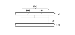
- FIG. 2A is a cross-sectional view showing a configuration of a transfer stamp according to an embodiment of the present invention.
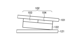
- FIG. 2B is a cross-sectional view showing the configuration of a transfer stamp according to an embodiment of the present invention.
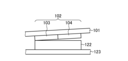
- FIG. 2C is a cross-sectional view showing a configuration of a transfer stamp according to an embodiment of the present invention.
- FIG. 2D is a cross-sectional view showing a configuration of a transfer stamp according to an embodiment of the present invention.
- This transfer stamp comprises a substrate 101 and a convex portion 102 formed on the substrate 101.
- the convex portion 102 comprises a main portion 103 and a sub-portion 104.
- the sub-portion 104 has a shape in which the width in a plan view decreases the further away it is from the main portion 103.
- the main portion 103 may have a rectangular shape in plan view, and the sub-portion 104 may have a square shape in plan view. Furthermore, the length of the main portion 103 in plan view at the boundary between the main portion 103 and the sub-portion 104 may be equal to the length of the sub-portion 104 in plan view.
- the sub-portion 104 may have a trapezoidal shape in plan view with the boundary with the main portion 103 as the base.
- the substrate 101 may be, for example, a glass substrate.
- the convex portion 102 may be made of a synthetic resin having viscoelasticity, such as polydimethylsiloxane (PDMS). In addition to the convex portion 102, the substrate 101 may be made of PDMS.
- the convex portion 102 may be formed by printing a pattern of a predetermined material on the substrate 101 by soft lithography using a mold made of a processed silicon substrate.
- convex portion 102 is brought into contact with the upper surface of element 122 formed on semiconductor substrate 121, and element 122 is attached to convex portion 102.
- convex portion 102 is made of a synthetic resin having viscoelasticity, element 122 will adhere to the upper surface of convex portion 102, and element 122 can be attached to convex portion 102 as described above.
- pick-up is performed by peeling off the transfer stamp from the main portion 103 side of the convex portion 102.
- the contact area between the element 122 and the convex portion 102 is equal to the contact area between the element 122 and the semiconductor substrate 121.
- the force acting between the element 122 and the convex portion 102 is made somewhat larger than the force acting between the element 122 and the semiconductor substrate 121, it becomes possible to pull the element 122 away from the semiconductor substrate 121 and pick it up with the convex portion 102 (transfer stamp).
- the contact area between the element 122 and the protruding portion 102 is smaller than the contact area between the element 122 and the other substrate 123.
- force acting between the element 122 and the main portion 103 > force acting between the element 122 and the semiconductor substrate 121 > force acting between the element 122 and the secondary portion 104 This makes it possible to prevent the element 122 from moving away from the other substrate 123, and to separate the protruding portion 102 from the element 122.
- the secondary portion of the protrusion to which the element is attached is shaped so that its width in plan view decreases the further it is from the primary portion, making it possible to achieve both good pick-up force and ease of release.
- 101 substrate, 102: protruding portion, 103: main portion, 104: secondary portion.
Landscapes
- Manufacturing Of Printed Wiring (AREA)
Priority Applications (2)
| Application Number | Priority Date | Filing Date | Title |
|---|---|---|---|
| JP2025512241A JPWO2024209537A1 (https=) | 2023-04-04 | 2023-04-04 | |
| PCT/JP2023/013931 WO2024209537A1 (ja) | 2023-04-04 | 2023-04-04 | 転写スタンプ |
Applications Claiming Priority (1)
| Application Number | Priority Date | Filing Date | Title |
|---|---|---|---|
| PCT/JP2023/013931 WO2024209537A1 (ja) | 2023-04-04 | 2023-04-04 | 転写スタンプ |
Publications (1)
| Publication Number | Publication Date |
|---|---|
| WO2024209537A1 true WO2024209537A1 (ja) | 2024-10-10 |
Family
ID=92971581
Family Applications (1)
| Application Number | Title | Priority Date | Filing Date |
|---|---|---|---|
| PCT/JP2023/013931 Ceased WO2024209537A1 (ja) | 2023-04-04 | 2023-04-04 | 転写スタンプ |
Country Status (2)
| Country | Link |
|---|---|
| JP (1) | JPWO2024209537A1 (https=) |
| WO (1) | WO2024209537A1 (https=) |
Citations (3)
| Publication number | Priority date | Publication date | Assignee | Title |
|---|---|---|---|---|
| JP2007027693A (ja) * | 2005-06-02 | 2007-02-01 | Board Of Trustees Of The Univ Of Illinois | エラストマースタンプへの接着の動的コントロールによるパターン転送印刷 |
| JP2017524250A (ja) * | 2014-07-20 | 2017-08-24 | エックス−セレプリント リミテッドX−Celeprint Limited | マイクロ転写印刷のための装置および方法 |
| JP2022002279A (ja) * | 2020-06-22 | 2022-01-06 | Tdk株式会社 | スタンプツールおよび素子アレイの製造方法 |
-
2023
- 2023-04-04 JP JP2025512241A patent/JPWO2024209537A1/ja active Pending
- 2023-04-04 WO PCT/JP2023/013931 patent/WO2024209537A1/ja not_active Ceased
Patent Citations (3)
| Publication number | Priority date | Publication date | Assignee | Title |
|---|---|---|---|---|
| JP2007027693A (ja) * | 2005-06-02 | 2007-02-01 | Board Of Trustees Of The Univ Of Illinois | エラストマースタンプへの接着の動的コントロールによるパターン転送印刷 |
| JP2017524250A (ja) * | 2014-07-20 | 2017-08-24 | エックス−セレプリント リミテッドX−Celeprint Limited | マイクロ転写印刷のための装置および方法 |
| JP2022002279A (ja) * | 2020-06-22 | 2022-01-06 | Tdk株式会社 | スタンプツールおよび素子アレイの製造方法 |
Also Published As
| Publication number | Publication date |
|---|---|
| JPWO2024209537A1 (https=) | 2024-10-10 |
Similar Documents
| Publication | Publication Date | Title |
|---|---|---|
| US10252514B2 (en) | Apparatus and methods for micro-transfer-printing | |
| US20200335381A1 (en) | Multi-level micro-device tethers | |
| US9887119B1 (en) | Multi-chip package assembly | |
| US20170207193A1 (en) | Apparatus and methods for micro-transfer-printing | |
| CN106601661B (zh) | 转印装置及转印方法 | |
| KR20190076690A (ko) | 변형필름을 이용한 전사방법 | |
| US10847673B2 (en) | Coupling a semiconductor component to a target substrate by transfer printing | |
| US8158048B2 (en) | Mold for fine pattern transfer and method for forming resin pattern using same | |
| US10930528B2 (en) | Method for transferring micro device | |
| KR20210019373A (ko) | 레이저를 이용한 개별 소자들의 전사 방법 | |
| WO2024209537A1 (ja) | 転写スタンプ | |
| JP4473233B2 (ja) | ソフトモールド及びその製造方法並びにこれを利用したパターニング方法 | |
| KR20140038309A (ko) | 금속-임베디드 포토마스크 및 그 제조 방법 | |
| US5846596A (en) | Methods of forming field oxide isolation regions having sloped edges | |
| CN111628053B (zh) | 微型发光二极管载板 | |
| JP2003218191A (ja) | 保護テープ及びその剥離方法 | |
| TWI716977B (zh) | 轉置頭 | |
| CN119230394B (zh) | 降低iii族氮化物半导体键合片中随机裂纹的方法 | |
| KR102340900B1 (ko) | 앵커를 이용하는 개별 소자들의 전사 방법 | |
| KR100600371B1 (ko) | 발광 소자의 제조 방법 | |
| EP4102543A1 (en) | A method for transferring a layer to a substrate | |
| TW202527080A (zh) | 半導體堆疊體及半導體裝置的製造方法 |
Legal Events
| Date | Code | Title | Description |
|---|---|---|---|
| 121 | Ep: the epo has been informed by wipo that ep was designated in this application |
Ref document number: 23931949 Country of ref document: EP Kind code of ref document: A1 |
|
| ENP | Entry into the national phase |
Ref document number: 2025512241 Country of ref document: JP Kind code of ref document: A |
|
| WWE | Wipo information: entry into national phase |
Ref document number: 2025512241 Country of ref document: JP |
|
| NENP | Non-entry into the national phase |
Ref country code: DE |
|
| 122 | Ep: pct application non-entry in european phase |
Ref document number: 23931949 Country of ref document: EP Kind code of ref document: A1 |