WO2024204135A1 - 表示装置、表示装置の駆動方法および電子機器 - Google Patents
表示装置、表示装置の駆動方法および電子機器 Download PDFInfo
- Publication number
- WO2024204135A1 WO2024204135A1 PCT/JP2024/011834 JP2024011834W WO2024204135A1 WO 2024204135 A1 WO2024204135 A1 WO 2024204135A1 JP 2024011834 W JP2024011834 W JP 2024011834W WO 2024204135 A1 WO2024204135 A1 WO 2024204135A1
- Authority
- WO
- WIPO (PCT)
- Prior art keywords
- period
- divided
- display device
- light
- pixel
- Prior art date
- Legal status (The legal status is an assumption and is not a legal conclusion. Google has not performed a legal analysis and makes no representation as to the accuracy of the status listed.)
- Ceased
Links
Images


Classifications
-
- G—PHYSICS
- G09—EDUCATION; CRYPTOGRAPHY; DISPLAY; ADVERTISING; SEALS
- G09G—ARRANGEMENTS OR CIRCUITS FOR CONTROL OF INDICATING DEVICES USING STATIC MEANS TO PRESENT VARIABLE INFORMATION
- G09G3/00—Control arrangements or circuits, of interest only in connection with visual indicators other than cathode-ray tubes
- G09G3/20—Control arrangements or circuits, of interest only in connection with visual indicators other than cathode-ray tubes for presentation of an assembly of a number of characters, e.g. a page, by composing the assembly by combination of individual elements arranged in a matrix no fixed position being assigned to or needed to be assigned to the individual characters or partial characters
- G09G3/22—Control arrangements or circuits, of interest only in connection with visual indicators other than cathode-ray tubes for presentation of an assembly of a number of characters, e.g. a page, by composing the assembly by combination of individual elements arranged in a matrix no fixed position being assigned to or needed to be assigned to the individual characters or partial characters using controlled light sources
- G09G3/30—Control arrangements or circuits, of interest only in connection with visual indicators other than cathode-ray tubes for presentation of an assembly of a number of characters, e.g. a page, by composing the assembly by combination of individual elements arranged in a matrix no fixed position being assigned to or needed to be assigned to the individual characters or partial characters using controlled light sources using electroluminescent panels
- G09G3/32—Control arrangements or circuits, of interest only in connection with visual indicators other than cathode-ray tubes for presentation of an assembly of a number of characters, e.g. a page, by composing the assembly by combination of individual elements arranged in a matrix no fixed position being assigned to or needed to be assigned to the individual characters or partial characters using controlled light sources using electroluminescent panels semiconductive, e.g. using light-emitting diodes [LED]
- G09G3/3208—Control arrangements or circuits, of interest only in connection with visual indicators other than cathode-ray tubes for presentation of an assembly of a number of characters, e.g. a page, by composing the assembly by combination of individual elements arranged in a matrix no fixed position being assigned to or needed to be assigned to the individual characters or partial characters using controlled light sources using electroluminescent panels semiconductive, e.g. using light-emitting diodes [LED] organic, e.g. using organic light-emitting diodes [OLED]
- G09G3/3225—Control arrangements or circuits, of interest only in connection with visual indicators other than cathode-ray tubes for presentation of an assembly of a number of characters, e.g. a page, by composing the assembly by combination of individual elements arranged in a matrix no fixed position being assigned to or needed to be assigned to the individual characters or partial characters using controlled light sources using electroluminescent panels semiconductive, e.g. using light-emitting diodes [LED] organic, e.g. using organic light-emitting diodes [OLED] using an active matrix
- G09G3/3233—Control arrangements or circuits, of interest only in connection with visual indicators other than cathode-ray tubes for presentation of an assembly of a number of characters, e.g. a page, by composing the assembly by combination of individual elements arranged in a matrix no fixed position being assigned to or needed to be assigned to the individual characters or partial characters using controlled light sources using electroluminescent panels semiconductive, e.g. using light-emitting diodes [LED] organic, e.g. using organic light-emitting diodes [OLED] using an active matrix with pixel circuitry controlling the current through the light-emitting element
-
- H—ELECTRICITY
- H05—ELECTRIC TECHNIQUES NOT OTHERWISE PROVIDED FOR
- H05B—ELECTRIC HEATING; ELECTRIC LIGHT SOURCES NOT OTHERWISE PROVIDED FOR; CIRCUIT ARRANGEMENTS FOR ELECTRIC LIGHT SOURCES, IN GENERAL
- H05B33/00—Electroluminescent light sources
- H05B33/12—Light sources with substantially two-dimensional [2D] radiating surfaces
- H05B33/14—Light sources with substantially two-dimensional [2D] radiating surfaces characterised by the chemical or physical composition or the arrangement of the electroluminescent material, or by the simultaneous addition of the electroluminescent material in or onto the light source
-
- H—ELECTRICITY
- H10—SEMICONDUCTOR DEVICES; ELECTRIC SOLID-STATE DEVICES NOT OTHERWISE PROVIDED FOR
- H10K—ORGANIC ELECTRIC SOLID-STATE DEVICES
- H10K50/00—Organic light-emitting devices
- H10K50/10—OLEDs or polymer light-emitting diodes [PLED]
-
- H—ELECTRICITY
- H10—SEMICONDUCTOR DEVICES; ELECTRIC SOLID-STATE DEVICES NOT OTHERWISE PROVIDED FOR
- H10K—ORGANIC ELECTRIC SOLID-STATE DEVICES
- H10K50/00—Organic light-emitting devices
- H10K50/10—OLEDs or polymer light-emitting diodes [PLED]
- H10K50/11—OLEDs or polymer light-emitting diodes [PLED] characterised by the electroluminescent [EL] layers
- H10K50/115—OLEDs or polymer light-emitting diodes [PLED] characterised by the electroluminescent [EL] layers comprising active inorganic nanostructures, e.g. luminescent quantum dots
-
- H—ELECTRICITY
- H10—SEMICONDUCTOR DEVICES; ELECTRIC SOLID-STATE DEVICES NOT OTHERWISE PROVIDED FOR
- H10K—ORGANIC ELECTRIC SOLID-STATE DEVICES
- H10K59/00—Integrated devices, or assemblies of multiple devices, comprising at least one organic light-emitting element covered by group H10K50/00
- H10K59/10—OLED displays
- H10K59/12—Active-matrix OLED [AMOLED] displays
Definitions
- This technology relates to a display device, a method for driving a display device, and electronic equipment.
- Such light-emitting elements include organic light-emitting diodes (OLEDs), also known as organic EL (Electro Luminescent) elements and light-emitting polymer elements.
- OLEDs organic light-emitting diodes
- EL Electro Luminescent
- Patent Document 1 The technology in Patent Document 1 is effective in suppressing flicker, but there is a demand for further improvements in the flicker suppression effect.
- This technology has been developed in consideration of these problems, and aims to provide a display device, a method for driving a display device, and electronic equipment that can prevent the occurrence of flicker.
- the first technology is a display device that includes a pixel region in which multiple pixels are arranged, and a light emission control unit that controls whether the pixels emit light or not, and adjusts the length of the pixel emission period in a divided period in which one frame of a displayed image is divided into multiple periods by controlling the pixel emission and non-emission.
- the second technology is a method for driving a display device that includes a pixel region in which multiple pixels are arranged and a light emission control unit that controls whether the pixels emit light or not, and adjusts the length of the pixel emission period in a divided period in which one frame of a displayed image is divided into multiple periods by controlling the emission and non-emission of the pixels.
- the third technology is an electronic device having a display device that includes a pixel region in which multiple pixels are arranged, and a light emission control unit that controls whether the pixels emit light or not, and that adjusts the length of the pixel emission period in a divided period in which one frame of a displayed image is divided into multiple periods by controlling the emission and non-emission of the pixels.
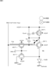
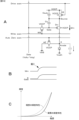
- FIG. 1 is a diagram showing an example of a schematic configuration of a typical display device 10.
- 1 is a diagram showing an example of the configuration and operation of a pixel circuit included in a general display device 10.
- FIG. 1 is a diagram showing an example of the configuration and operation of a pixel circuit included in a general display device 10.
- FIG. 2 is a diagram showing an example of a timing chart in a pixel circuit of a general display device 10.
- FIG. 1 is an explanatory diagram of a problem to be considered in the first embodiment.
- FIG. 4 is a pixel circuit diagram for explaining a problem to be considered in the first embodiment.
- FIG. 1 is an explanatory diagram of a problem to be considered in the first embodiment.
- FIG. 1 is an explanatory diagram of a problem to be considered in the first embodiment.
- 1 is a diagram showing a configuration of a display system 100 according to a first embodiment.
- FIG. 2 is a control sequence diagram in the display system 100.
- FIG. 2 is a control sequence diagram in the display system 100.
- 5A and 5B are diagrams illustrating a first example of a light emission period and a change in luminance in the first embodiment.
- 11A and 11B are diagrams illustrating a second example of a light emission period and a change in luminance in the first embodiment.
- FIG. 11 is an explanatory diagram of a problem to be considered in the second embodiment.
- 13A and 13B are diagrams illustrating a light emission period and a change in luminance in the second embodiment.
- FIG. 13 is an explanatory diagram of a problem to be considered in the third embodiment.
- 13A and 13B are diagrams illustrating a light emission period and a change in luminance in the third embodiment.
- FIG. 1 is a perspective view showing an example of the appearance of a head mounted display. 1 is a perspective view showing an example of the appearance of a see-through head mounted display.
- FIG. 1A is a front view showing an example of the external appearance of a digital still camera
- FIG. 1 is a perspective view showing an example of the appearance of a television device.
- FIG. 1 is a perspective view showing an example of the appearance of a smartphone.
- 1A is a diagram showing an example of the interior of a vehicle from the rear to the front of the vehicle
- FIG. 1B is a diagram showing an example of the interior of a vehicle from the diagonally rear to the diagonally front of the vehicle.
- FIG. 1 shows an example of the schematic configuration of a typical display device 10.
- the display device 10 is, for example, an organic EL (Electro Luminescence) display device equipped with an active matrix type drive circuit and using OLEDs as light-emitting elements. Note that the display device 10 may also use other light-emitting elements such as micro LEDs (Light Emitting Diodes) and quantum dot light-emitting elements.
- OLED Electro Luminescence
- the display device 10 may also use other light-emitting elements such as micro LEDs (Light Emitting Diodes) and quantum dot light-emitting elements.
- the display device 10 includes a pixel array section 11 provided on a display panel, in which a plurality of pixels PIX, each including an organic EL element, are arranged two-dimensionally in a matrix.
- the display device 10 also includes a write scanning section 12, a drive scanning section 13, and a signal output section 14, which are mounted on the same display panel as the pixel array section 11 and are arranged around the pixel array section 11.
- the pixel array section 11 is a pixel region in which multiple pixels PIX are arranged two-dimensionally in a matrix.
- multiple scanning lines L1 and drive lines L2 are wired for each pixel PIX row along the row direction (the direction in which the pixels in the pixel row are arranged) for the matrix-like arrangement of the pixels PIX.
- multiple signal lines SIG are wired for each pixel column along the column direction (the direction in which the pixels in the pixel column are arranged) for the matrix-like arrangement of the pixels PIX.
- the pixel PIX includes a light-emitting element OLED, which is an example of a light-emitting element, and a pixel circuit.
- the scanning line L1 is connected to the output terminal of the corresponding row of the write scanning unit 12.
- the drive line L2 is connected to the output terminal of the corresponding row of the drive scanning unit 13.
- the signal line SIG is connected to the output terminal of the corresponding column of the signal output unit 14.
- the pixel array section 11 is provided with pixels PIX (also called sub-pixels) corresponding to the three primary color pixels of R (red), G (green), and B (blue). These three pixels represent one dot of a color image. Note that the combination of pixels that represent one dot is not limited to this, and it may be configured by adding a W (white) pixel to improve brightness, or a complementary color pixel to expand the color reproduction range. Furthermore, the pixel PIX is not limited to a color image, and may be configured to represent a monochrome (black and white) image.
- the write scanning unit 12 has a write scanner (Write Scan) and an auto zero scanner (Auto Zero Scan).
- the write scanning unit 12 sequentially supplies a write scanning signal (signal WS) and a control signal (signal AZ) to the scanning line L1, thereby scanning each pixel PIX of the pixel array unit 11 in sequence on a row-by-row basis.
- the write scanning unit 12 is composed of a shift register circuit, etc.
- the pixel circuit that drives the light-emitting element OLED is configured to include a WS transistor, a DS transistor, a DR transistor, an AZ transistor, a storage capacitance Cs, an auxiliary capacitance Csub, and the light-emitting element OLED. That is, the pixel circuit in this example is a pixel circuit with a 4Tr (Transistor) 2C (Capacitor) configuration.
- the WS transistor, DS transistor, DR transistor, and AZ transistor are, for example, P-type MOSFETs (Metal Oxide Semiconductor Field Effect Transistors). Each transistor has four terminals: source, gate, and drain/backgate, and the backgate of each transistor is connected to the power supply line VCCP.
- the gate of the DS transistor is connected to the drive line L2, the source is connected to the power supply line VCCP, and the drain is connected to the source of the DR transistor, the other end of the auxiliary capacitance Csub, and one end of the holding capacitance Cs.
- the gate of the DR transistor is connected to the drain of the WS transistor and the other end of the holding capacitance Cs, the source is connected to the drain of the DS transistor, the other end of the auxiliary capacitance Csub, and one end of the holding capacitance Cs, and the drain is connected to the anode of the light-emitting element OLED and the source of the AZ transistor.
- the light-emitting element OLED is an organic EL light-emitting element, with one end, the anode, connected to the drain of the DR transistor and the source of the AZ transistor, and the other end being the cathode.
- the timing chart in Fig. 4 shows the temporal transitions of the signal WS and signal AZ supplied to the scanning line L1, the signal DS supplied to the drive line L2, the potentials Vref/Vofs/Vsig of the signal line SIG, and the source voltage Vs of the DR transistor, the gate voltage Vg, and the anode of the light-emitting element OLED (the drain voltage of the DR transistor).
- one horizontal period (1H) is made up of five periods (initialization, Vth correction, writing, light emission, and extinction).
- the signals WS and AZ go from high to low, the light emission period ends, and the initialization period (t1 to t2) begins, during which the DR transistor is initialized.
- the signals WS and AZ go high, and the reference voltage Vref drops to the standard voltage Vofs.
- the signal DS goes high.
- the signals WS and AZ go low, entering a Vth correction period in which the threshold voltage Vth of the DR transistor, which may vary in each pixel PIX, is corrected.
- the next write period is a period during which the signal voltage Vsig corresponding to the video signal is written to the pixel PIX, as shown in Figure 2.
- the signal WS goes from high to low, and the WS transistor goes from off to on, causing the gate voltage Vg of the DR transistor to become the signal voltage of the signal line SIG.
- the signal voltage Vsig is applied to the signal line SIG, and the gate voltage Vg of the DR transistor becomes the signal voltage Vsig.
- the storage capacitor Cs holds the signal voltage Vsig written by the WS transistor.
- the signal WS goes high, turning off the WS transistor, and the write period of the signal voltage Vsig to the DR transistor ends.
- the signal DS goes from high to low, and the DS transistor goes from off to on, entering the light emission period.
- the DS transistor turns on, causing a drain-source current Ids corresponding to the gate-source voltage Vgs held in the storage capacitance Cs to flow through the light emitting element OLED, causing the light emitting element OLED to emit light.
- the DS transistor When the DS transistor is turned off, no current is supplied from the DR transistor to the light-emitting element OLED, and the light-emitting element OLED is in a non-emitting state. In other words, the period during which the DS transistor is off is the non-emitting period of the light-emitting element OLED.
- Fig. 5A shows a write period and a light emission period extracted from a timing chart when the image displayed by the display device 10 has a high frame rate.
- Fig. 5B shows a write period and a light emission period extracted from a timing chart when the image displayed by the display device 10 has a low frame rate.
- a high frame rate is a frame rate of 30 Hz or more
- a low frame rate is a frame rate of less than 30 Hz.
- this technology is not limited to these values.
- the light emission period is longer than at high frame rates, and therefore the period during which the gate voltage Vg of the DR transistor rises is also longer than at high frame rates during the light emission period, and the amount of rise in the gate voltage Vg increases.
- the amount of rise in the gate voltage Vg of the DR transistor increases due to leakage from the WS transistor.
- the gate-source voltage Vgs of the DR transistor decreases, and this decrease reduces the drain-source current Ids, which results in a decrease in the luminance of the light-emitting element OLED and a decrease in the luminance of the pixel PIX.
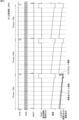
- Figure 7 shows the changes in the vertical synchronization signal XVD, horizontal synchronization signal XHD, signal WSST, signal DSST, and brightness of pixel PIX for each frame of video during normal video display on display device 10.
- FIG. 8 there is a method of dividing the light emission period (light emission duty) of pixel PIX, as shown in Figure 8.
- one frame (15 Hz) of an image displayed by the display device 10 is divided into eight divided periods. Each divided period is set to 120 Hz.
- the light emission period of pixel PIX in each divided period is then uniformly shortened. In Figure 8, it is set to 30% as an example.
- This light emission period ratio is the ratio when the length of the light emission period in the last divided period in one frame (the eighth divided period in Figure 9) is set to 100%.
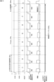
- the display system 100 is composed of a display device 10, a data input I/F unit 20, a timing controller 30, and a display controller 40.
- the display device 10 is configured with a pixel array section 11, a V-DRV 15, an H-DRV 16, and a signal processing section 17.
- the pixel array section 11 has a plurality of pixel circuits arranged in the horizontal and vertical directions.
- the configurations of the pixel array section 11 and the pixel circuits are similar to those described with reference to Figures 1 and 2.
- the V-DRV 15 has a write scanning unit 12 and a drive scanning unit 13. As described above, when writing the signal voltage of the video signal to each pixel PIX of the pixel array unit 11, the write scanning unit 12 sequentially supplies the signal WS and the signal AZ to the scanning line L1, thereby scanning each pixel PIX of the pixel array unit 11 in sequence by row.
- the drive scanning unit 13 controls the emission/non-emission (extinction) of the pixels PIX by supplying a light emission control signal (signal DS) to each drive line L2 in synchronization with the line sequential scanning by the write scanning unit 12.
- the H-DRV 16 has a signal output unit 14. As described above, the signal output unit 14 selectively outputs a reference voltage Vref, a signal voltage Vsig, and a standard voltage Vofs, which are supplied to each pixel PIX via a signal line SIG and written in units of pixel rows selected by scanning by the write scanning unit 12.
- the signal processing unit 17 processes the video signal displayed on the pixel array unit 11.
- the signal processing unit 17 performs gamma correction based on the brightness adjustment signal from the timing controller 30.
- the video signal processed by the signal processing unit 17 is supplied to the H-DRV 16.
- the data input I/F section 20 comprises an LVDS (Low voltage differential signaling) I/F 21, a data S/P 22, a clock control section 23, and an H/V synchronization section 24.
- the LVDS I/F 21 section receives a video signal from the outside.
- the data S/P 22 converts the video signal into parallel data and then supplies it to the image processing section 33 of the timing controller 30.
- the clock control section 23 generates a clock that matches the display frequency of the display device 10.
- the H/V synchronization section 24 generates a signal that specifies the horizontal synchronization timing and vertical synchronization timing of the display device 10 and supplies it to the timing generator 32.
- the timing controller 30 has a clock generation function and a timing generation function, generates a vertical synchronization clock and a horizontal synchronization clock for the display device 10, and supplies them to the VLOGIC 42 of the display controller 40.
- the timing controller 30 also generates a signal that specifies the operation timing of the display controller 40, and supplies it to the VLOGIC 42 of the display controller 40.
- the timing controller 30 supplies the VLOGIC 42 with a signal WSST1 that specifies the write start position, a signal DSST that specifies the light emission period in the L period, and a signal AZST that specifies the extinction period in the L period.
- the timing controller 30 generates a signal DSST that specifies the light emission period according to the present technology, which will be described later, by changing the internal settings (register). The light emission period of the pixel PIX in the present technology is adjusted by the timing controller 30.
- the timing controller 30 also has an image processing function and performs a predetermined signal processing on the video signal input from the data S/P 22.
- the processed video signal is supplied to the HLOGIC 41 of the display controller 40.
- the display controller 40 includes an HLOGIC 41 and a VLOGIC 42, and performs display control for the pixel array unit 11.
- the HLOGIC 41 supplies a video signal to the H-DRV 16.
- the VLOGIC 42 Based on the signal input from the timing controller 30, the VLOGIC 42 generates a signal that specifies the timing of the scanning line L1 and the driving line L2, and supplies the signal to the V-DRV 15.
- the VLOGIC 42 supplies to the V-DRV 15 a signal WSSR that controls the write timing of each line in the H period, a signal DSSR that controls the light emission timing of each line in the L period, and a signal AZSR that controls the light extinction timing of each line in the L period.
- V-DRV 15 supplies the pixel circuit with a signal WS that controls the write timing during the L period, a signal DS that controls the light emission timing during the L period, and a signal AZ that controls the extinction timing during the L period.
- the interface 50 connects the data input IF to external devices and networks, and can be, for example, a MIPI (Mobile Industry Processor Interface).
- MIPI Mobile Industry Processor Interface
- FIG. 12 is a diagram showing the changes in the vertical synchronization signal XVD, horizontal synchronization signal XHD, signal WSST, signal DSST, and luminance of pixel PIX for each frame of a low frame rate image displayed on display device 10 in the first embodiment, and the adjustment of the light emission period.
- signal WSST is a signal that specifies the start position of writing
- signal DSST is a signal that specifies the light emission period of pixel PIX.
- a low frame rate is defined as a frame rate of less than 30 Hz.
- the entire period of one frame (15 Hz) (one vertical scan period) is the light emission period of the pixel PIX, and one frame is divided into periods shorter than the response period of the human eye so that the period is shorter than the response period of the human eye.
- one frame is divided into eight division periods, and each division period is 120 Hz.
- the response period of the human eye is approximately 60 Hz.
- the length of time that the signal DSST is turned on for each frame i.e., the light emission period of the pixel PIX, is gradually lengthened over time.
- the light emitting period of the first divided period which is the first divided period
- the light emitting period of the second divided period is set to 40%.
- the light emitting period of the third divided period is set to 50%.
- the light emitting period of the fourth divided period is set to 60%.
- the light emitting period of the fifth divided period is set to 70%.
- the light emitting period of the sixth divided period is set to 80%.
- the light emitting period of the seventh divided period is set to 90%.
- the light emitting period of the eighth divided period, which is the last divided period, is set to 100%. In other words, as time passes, the proportion of the light emitting duty in each divided period is gradually increased from the first divided period to the eighth divided period, which is the last divided period, and the light emitting period is adjusted so that it gradually becomes longer in stages.
- the timing controller 30 by changing the settings (register) of the timing controller 30 according to the amount of decrease in pixel PIX that is specified in advance by measurement or calculation, the timing controller 30 generates a signal DSST that specifies the light emission period and supplies it to the VLOGIC 42. Then, by supplying a signal DS, which is a light emission control signal, from the V-DRV 15 to the pixel circuit via the VLOGIC 42, the light emission/non-emission of the light emitting element OLED is controlled, and the length of the light emission period of the pixel PIX is adjusted.
- a signal DS which is a light emission control signal
- the brightness of pixel PIX decreases over time, so it is advisable to adjust the light-emitting period of pixel PIX so that it gradually becomes longer over time.
- the ratio of the length of the light emission period in each divided period is the ratio when the length of the light emission period in the last divided period in one frame (the eighth divided period in Figure 12) is taken as 100%.
- the light emission period of each division period is changed in stages by 10%, but this is merely one example. As long as the light emission period gradually becomes longer over time and the light emission period of the last division period reaches 100%, the light emission period can be changed in any way.
- one frame may be divided into multiple sub-periods that are shorter than the response period of the human eye (60 Hz), and the light emission period within each sub-period may be further divided. This also makes it possible to prevent a decrease in luminance and the occurrence of flicker, as in the case of FIG. 12.
- the light emitting period of the first divided period in which the light emitting period is 30%, is divided into 24% and 6%.
- the light emitting period of the second divided period, in which the light emitting period is 40% is divided into 32% and 8%.
- the light emitting period of the third divided period in which the light emitting period is 50%, is divided into 40% and 10%.
- the light emitting period of the fourth divided period in which the light emitting period is 60%, is divided into 48% and 12%.
- the light emitting period of the fifth divided period in which the light emitting period is 70%, is divided into 56% and 14%.
- the light emitting period of the sixth divided period, in which the light emitting period is 80% is divided into 64% and 16%.
- the light emitting period of the seventh divided period in which the light emitting period is 90%, is divided into 72% and 18%.
- the light emitting period of the eighth divided period in which the light emitting period is 100%, is divided into 80% and 20%.
- a first divided period having a light emitting period of 30% may be divided into 15% and 15%, or into 6% and 24%.
- the division method There are no limitations on the division method.
- the light emitting period in one divided period may be divided into three or more.
- the second embodiment prevents black floating.
- Black floating refers to a phenomenon in which light leakage occurs in some areas when black is displayed due to the luminance of the light-emitting element OLED becoming greater than the ideal characteristics. This causes the black in the pixel PIX to become pale, resulting in deterioration of contrast, etc.
- FIG. 15 is a diagram showing changes in the vertical synchronization signal XVD, the horizontal synchronization signal XHD, the signal WSST, the signal DSST, and the luminance of a pixel PIX for each frame of an image displayed on the display device 10 in the second embodiment, and adjustment of the light emission period.
- the period of one frame (e.g., 15 Hz) (one vertical scanning period) is divided into periods less than the response period of the human eye, as in the first embodiment.
- the light emission period of pixel PIX in the division period corresponding to the period in which the peak of the drive current Idrv occurs is shortened. This reduces the amount of light emitted in the division period corresponding to the period in which the peak of the drive current Idrv occurs, making it possible to prevent black floating caused by the peak at the beginning of the flow of the drive current Idrv.
- the light emission duty is increased stepwise over time in the same manner as in the first embodiment, and the light emission period is adjusted to become longer stepwise. Therefore, the light emission period of the second division period is set to 40%.
- the light emission period of the third division period is set to 50%.
- the light emission period of the fourth division period is set to 60%.
- the light emission period of the fifth division period is set to 70%.
- the light emission period of the sixth division period is set to 80%.
- the light emission period of the seventh division period is set to 90%.
- the light emission period of the eighth division period is set to 100%.
- the timing controller 30 by changing the settings (register) of the timing controller 30 according to the peak of the drive current Idrv, which is specified in advance by measurement or calculation, the timing controller 30 generates a signal DSST that controls the light emission period as described above and supplies it to the VLOGIC 42. Then, the signal DS is supplied from the V-DRV 15 to the pixel circuit, which controls the light emission/non-emission of the light emitting element OLED and adjusts the light emission period of the pixel PIX.
- the light emission period of pixel PIX in the first division period is set to 20%, but this is merely an example, and the extent to which the light emission period in the division period corresponding to the period in which the peak of the drive current Idrv occurs should be shortened can be set appropriately depending on the peak of the drive current Idrv.
- the third embodiment prevents black sunkenness.
- Black sunkenness refers to the phenomenon in which the luminance of the light-emitting element OLED becomes lower than the ideal characteristic, causing the light emitted by the light-emitting element OLED to become dark.
- FIG. 17 is a diagram showing changes in the vertical synchronizing signal XVD, the horizontal synchronizing signal XHD, the signal WSST, the signal DSST, and the luminance of a pixel PIX for each frame of a video, and adjustment of the light emitting period in the third embodiment.
- the period of one frame (15 Hz) (one vertical scanning period) is divided into periods shorter than the response period of the human eye, as in the first embodiment.
- the light emission period of the first division period which is the division period corresponding to the period during which the drive current Idrv slows, is made longer than in the first embodiment, at 40%.
- the timing controller 30 by changing the settings (register) of the timing controller 30 in response to the slowdown of the drive current Idrv that is specified in advance by measurement or calculation, the timing controller 30 generates a signal DSST that controls the light emission period as described above and supplies it to the VLOGIC 42. Then, the signal DS is supplied from the V-DRV 15 to the pixel circuit, which controls the light emission/non-emission of the light emitting element OLED and adjusts the light emission period of the pixel PIX.
- the light emission period of pixel PIX in the first division period is set to 40%, but this is merely an example, and the length of the light emission period of pixel PIX in the division period corresponding to the period in which the damping of the drive current Idrv occurs can be set appropriately depending on the damping of the drive current Idrv.
- the light emission period in the first division period is long, but in order to prevent black sunkenness, it is necessary to lengthen the light emission period of the light-emitting element OLED in the division period corresponding to the period in which the drive current Idrv slows. Therefore, for example, if the periods in which the drive current Idrv peaks are the first division period and the second division period, it is necessary to lengthen the light emission periods in those two division periods.
- the light emission period of each of the multiple divided periods is adjusted to become gradually longer from the second divided period to the last divided period, and the light emission period of the first divided period of the multiple divided periods is adjusted to be longer than or equal to the light emission period of the second divided period.
- the display device 10 according to the embodiment to which the present technology is applied may be provided in various electronic devices. Examples of application of the electronic device include the following.
- (Application Example 1) 18 shows an example of the appearance of a head mounted display 110.
- the head mounted display 110 has, for example, ear hooks 112 for wearing on the user's head on both sides of a glasses-shaped display unit 111.
- the display unit 111 includes the display device 10 described above.
- the see-through head mounted display 120 includes a main body 121, an arm 122, and a lens barrel 123.
- the main body 121 is connected to the arm 122 and the glasses 128. Specifically, the end of the long side of the main body 121 is connected to the arm 122, and one side of the main body 121 is connected to the glasses 128 via a connecting member. The main body 121 may also be worn directly on the head of the human body.
- the main body 121 incorporates a control board for controlling the operation of the see-through head mounted display 120, and a display unit.
- the arm 122 connects the main body 121 to the telescope tube 123 and supports the telescope tube 123. Specifically, the arm 122 is coupled to an end of the main body 121 and an end of the telescope tube 123, respectively, and fixes the telescope tube 123.
- the arm 122 also incorporates a signal line SIG for communicating data related to images provided from the main body 121 to the telescope tube 123.
- this see-through head mounted display 120 is a so-called light guide plate type head mounted display, but is not limited to this and may be, for example, a so-called birdbath type head mounted display.
- This birdbath type head mounted display includes, for example, a beam splitter and a partially transparent mirror.
- the beam splitter outputs light encoded with image information toward the mirror, and the mirror reflects the light toward the user's eyes.
- Both the beam splitter and the partially transparent mirror are partially transparent. This allows light from the surrounding environment to reach the user's eyes.
- 20A and 20B show an example of the appearance of a digital still camera 138.
- This digital still camera 138 is a lens-interchangeable single-lens reflex type, and has an interchangeable photographing lens unit (interchangeable lens) 132 located approximately in the center of the front of a camera main body (camera body) 131, and a grip part 133 for the photographer to hold on the left side of the front.
- interchangeable photographing lens unit interchangeable lens
- a monitor 134 is provided at a position shifted to the left from the center on the back of the camera body 131.
- An electronic viewfinder (eyepiece window) 135 is provided at the top of the monitor 134. By looking through the electronic viewfinder 135, the photographer can visually confirm the optical image of the subject guided by the photographing lens unit 132 and determine the composition.
- the electronic viewfinder 135 is equipped with the display device 10 described above.
- (Application Example 4) 21 shows an example of the appearance of a television device 140.
- This television device 140 has an image display screen unit 141 including, for example, a front panel 142 and a filter glass 143, and this image display screen unit 141 is equipped with the display device 10 described above.
- the smartphone 150 includes a display unit 151 that displays various information, and an operation unit 152 that includes buttons and the like that accept operation inputs by a user.
- the display unit 151 includes the display device 10 described above.
- FIG. 23A and 23B are diagrams showing an example of the internal configuration of a vehicle 200 equipped with various displays. Specifically, FIG. 23A is a diagram showing an example of the interior of the vehicle 200 from the rear to the front, and FIG. 23B is a diagram showing an example of the interior of the vehicle 200 from diagonally rear to diagonally front.
- the vehicle 200 includes a center display 201, a console display 202, a head-up display 203, a digital rear mirror 204, a steering wheel display 205, and a rear entertainment display 206. At least one of these displays includes the display device 10 described above. For example, all of these displays may include the display device 10 described above.
- the center display 201 is disposed in a portion of the dashboard facing the driver's seat 208 and the passenger seat 209.
- Figs. 23A and 23B show an example of a horizontally elongated center display 201 extending from the driver's seat 208 side to the passenger seat 209 side
- the screen size and location of the center display 201 are arbitrary.
- the center display 201 can display information detected by various sensors. As a specific example, the center display 201 can display an image captured by an image sensor, an image of the distance to an obstacle in front of or to the side of the vehicle 200 measured by a ToF sensor, and the body temperature of a passenger detected by an infrared sensor.
- the center display 201 can be used to display, for example, at least one of safety-related information, operation-related information, a life log, health-related information, authentication/identification-related information, and entertainment-related information.
- the safety-related information includes information such as detection of drowsiness, detection of distraction, detection of tampering by children in the vehicle, whether or not a seat belt is fastened, and detection of an occupant being left behind, and is information detected, for example, by a sensor arranged on the back side of the center display 201.
- the operation-related information is obtained by detecting gestures related to the operation of the occupant using a sensor.
- the detected gestures may include operations of various facilities in the vehicle 200. For example, operations of air conditioning equipment, navigation equipment, AV equipment, lighting equipment, etc. are detected.
- the life log includes the life log of all occupants. For example, the life log includes a record of the actions of each occupant while on board.
- the health-related information is obtained by detecting the body temperature of the occupant using a sensor such as a temperature sensor, and inferring the health condition of the occupant based on the detected body temperature.
- a sensor such as a temperature sensor
- the face of the occupant may be captured using an image sensor, and the health condition of the occupant may be inferred from the facial expression captured in the image.
- the occupant may be spoken to by an automated voice and the occupant's health condition may be inferred based on the occupant's responses.
- Authentication/identification related information includes a keyless entry function that uses a sensor to perform face authentication, and a function that automatically adjusts the seat height and position by face recognition.
- Entertainment related information includes a function that uses a sensor to detect information about the operation of an AV device by an occupant, and a function that recognizes the occupant's face with a sensor and provides content suitable for the occupant via the AV device.
- the console display 202 can be used, for example, to display life log information.
- the console display 202 is disposed near the shift lever 211 on the center console 210 between the driver's seat 208 and the passenger seat 209. Information detected by various sensors can also be displayed on the console display 202.
- the console display 202 may display an image of the surroundings of the vehicle captured by an image sensor, or may display an image showing the distance to obstacles around the vehicle.
- the head-up display 203 is virtually displayed behind the windshield 212 in front of the driver's seat 208.
- the head-up display 203 can be used to display, for example, at least one of safety-related information, operation-related information, a life log, health-related information, authentication/identification-related information, and entertainment-related information. Since the head-up display 203 is often virtually positioned in front of the driver's seat 208, it is suitable for displaying information directly related to the operation of the vehicle 200, such as the speed of the vehicle 200 and the remaining fuel (battery) level.
- the digital rear-view mirror 204 can not only display the rear of the vehicle 200, but also display the state of passengers in the back seats. Therefore, by placing a sensor on the back side of the digital rear-view mirror 204, it can be used to display life log information, for example.
- the steering wheel display 205 is disposed near the center of the steering wheel 213 of the vehicle 200.
- the steering wheel display 205 can be used to display, for example, at least one of safety-related information, operation-related information, life log, health-related information, authentication/identification-related information, and entertainment-related information.
- the steering wheel display 205 since the steering wheel display 205 is located near the driver's hands, it is suitable for displaying life log information such as the driver's body temperature, and for displaying information related to the operation of AV equipment, air conditioning equipment, etc.
- the rear entertainment display 206 is attached to the back side of the driver's seat 208 and passenger seat 209, and is intended for viewing by rear seat passengers.
- the rear entertainment display 206 can be used to display at least one of safety-related information, operation-related information, life log, health-related information, authentication/identification-related information, and entertainment-related information, for example.
- information related to the rear seat passengers is displayed on the rear entertainment display 206.
- the rear entertainment display 206 may display information related to the operation of AV equipment or air conditioning equipment, or may display the results of measuring the body temperature of the rear seat passengers using a temperature sensor.
- a sensor may be placed on the back side of the display device 10 to measure the distance to surrounding objects.
- Optical distance measurement methods are broadly divided into passive and active types.
- Passive types measure distance by receiving light from an object without projecting light from the sensor onto the object.
- Passive types include the lens focusing method, the stereo method, and the monocular vision method.
- Active types measure distance by projecting light onto an object and receiving the light reflected from the object with a sensor.
- Active types include the optical radar method, the active stereo method, the photometric stereo method, the moire topography method, and the interference method.
- the display device 10 described above can be applied to any of these distance measurement methods. By using a sensor placed on the back side of the display device 10 described above, the above-mentioned passive or active distance measurement can be performed.
- the pixel array section 11 is described as being rectangular, but the shape of the pixel array section 11 is not limited to a rectangular shape, and can be a square shape, a circle shape, an ellipse shape, or a polygonal shape other than a rectangle.
- one frame is divided into eight divided periods, but the number of divided periods in one frame is not limited to eight, and may be more than eight or less than eight.
- the pixel PIX is not limited to the configuration example (including the modified example) described above, and can be modified as appropriate, such as by replacing a P-channel transistor with an N-channel transistor.
- the type, number, and connection of the transistors, capacitors, and light-emitting element OLED can be modified as appropriate.
- Various video signals and control signals can be generated accordingly and supplied to the pixel PIX.
- This technology is not limited to the pixel circuit with a 4Tr (Transistor) 2C (Capacitor) configuration shown in Figure 2, but can be applied to any display device that can adjust the light emission time by controlling the light emission/non-emission of the pixel PIX.
- the present technology can also be configured as follows. (1) a pixel region in which a plurality of pixels are arranged; A light emission control unit that controls whether the pixel emits light or not; Equipped with A display device that adjusts the length of a light emission period of the pixel in a divided period into which one frame of a displayed image is divided into a plurality of periods by controlling whether the pixel emits light or not. (2) The display device according to (1), wherein the light emission period of each of the plurality of divided periods is adjusted to become gradually longer from a first divided period to a last divided period among the plurality of divided periods. (3) The display device according to (1) or (2), wherein the division period is shorter than a response period of the human eye.
- the display device according to any one of (1) to (3), further comprising: a display unit configured to adjust a length of a light-emitting period of the pixel in the division period when a frame rate of the video is low.
- a display unit configured to adjust a length of a light-emitting period of the pixel in the division period when a frame rate of the video is low.
- the low frame rate of the video is equal to or lower than 30 Hz.
- the display device according to any one of (1) to (5), wherein the light emission period in a first division period of the plurality of division periods is shortened.
- the display device according to any one of (1) to (6), wherein the light emission period in a first division period of the plurality of division periods is lengthened.
- a pixel region in which a plurality of pixels are arranged a pixel region in which a plurality of pixels are arranged;
- a light emission control unit that controls whether the pixel emits light or not;
- a display device comprising: A display device driving method for adjusting the length of a light emission period of the pixel in a divided period obtained by dividing one frame of a displayed image into a plurality of periods by controlling the light emission and non-emission of the pixel.
- An electronic device comprising the display device according to any one of (1) to (12).
- Display device 11 Pixel array section 13: Drive scanning section
Landscapes
- Engineering & Computer Science (AREA)
- Physics & Mathematics (AREA)
- General Physics & Mathematics (AREA)
- Computer Hardware Design (AREA)
- Theoretical Computer Science (AREA)
- Optics & Photonics (AREA)
- Crystallography & Structural Chemistry (AREA)
- Inorganic Chemistry (AREA)
- Nanotechnology (AREA)
- Chemical & Material Sciences (AREA)
- Microelectronics & Electronic Packaging (AREA)
- Control Of Indicators Other Than Cathode Ray Tubes (AREA)
- Electroluminescent Light Sources (AREA)
Priority Applications (1)
| Application Number | Priority Date | Filing Date | Title |
|---|---|---|---|
| JP2025510893A JPWO2024204135A1 (https=) | 2023-03-30 | 2024-03-26 |
Applications Claiming Priority (2)
| Application Number | Priority Date | Filing Date | Title |
|---|---|---|---|
| JP2023-055485 | 2023-03-30 | ||
| JP2023055485 | 2023-03-30 |
Publications (1)
| Publication Number | Publication Date |
|---|---|
| WO2024204135A1 true WO2024204135A1 (ja) | 2024-10-03 |
Family
ID=92906587
Family Applications (1)
| Application Number | Title | Priority Date | Filing Date |
|---|---|---|---|
| PCT/JP2024/011834 Ceased WO2024204135A1 (ja) | 2023-03-30 | 2024-03-26 | 表示装置、表示装置の駆動方法および電子機器 |
Country Status (2)
| Country | Link |
|---|---|
| JP (1) | JPWO2024204135A1 (https=) |
| WO (1) | WO2024204135A1 (https=) |
Citations (4)
| Publication number | Priority date | Publication date | Assignee | Title |
|---|---|---|---|---|
| JP2003005708A (ja) * | 2001-04-20 | 2003-01-08 | Semiconductor Energy Lab Co Ltd | 表示装置および表示装置の駆動方法 |
| JP2012053447A (ja) * | 2010-08-06 | 2012-03-15 | Canon Inc | 表示装置及びその駆動方法 |
| JP2017227781A (ja) * | 2016-06-23 | 2017-12-28 | セイコーエプソン株式会社 | 電気光学装置、電気光学装置の駆動方法、および電子機器 |
| JP2018060124A (ja) * | 2016-10-07 | 2018-04-12 | 株式会社ジャパンディスプレイ | 表示装置 |
-
2024
- 2024-03-26 JP JP2025510893A patent/JPWO2024204135A1/ja active Pending
- 2024-03-26 WO PCT/JP2024/011834 patent/WO2024204135A1/ja not_active Ceased
Patent Citations (4)
| Publication number | Priority date | Publication date | Assignee | Title |
|---|---|---|---|---|
| JP2003005708A (ja) * | 2001-04-20 | 2003-01-08 | Semiconductor Energy Lab Co Ltd | 表示装置および表示装置の駆動方法 |
| JP2012053447A (ja) * | 2010-08-06 | 2012-03-15 | Canon Inc | 表示装置及びその駆動方法 |
| JP2017227781A (ja) * | 2016-06-23 | 2017-12-28 | セイコーエプソン株式会社 | 電気光学装置、電気光学装置の駆動方法、および電子機器 |
| JP2018060124A (ja) * | 2016-10-07 | 2018-04-12 | 株式会社ジャパンディスプレイ | 表示装置 |
Also Published As
| Publication number | Publication date |
|---|---|
| JPWO2024204135A1 (https=) | 2024-10-03 |
Similar Documents
| Publication | Publication Date | Title |
|---|---|---|
| KR20240158967A (ko) | 표시 장치 및 전자 기기 | |
| WO2022230578A1 (ja) | 表示装置及び電子機器 | |
| WO2022270300A1 (ja) | 表示装置 | |
| JP2023141871A (ja) | 発光装置、表示装置、光電変換装置、電子機器、照明装置、移動体およびウェアラブルデバイス | |
| WO2024084876A1 (ja) | 表示装置および電子機器 | |
| JP7832213B2 (ja) | 表示装置、電子機器、及び表示制御方法 | |
| WO2023243474A1 (ja) | 表示装置 | |
| WO2024204135A1 (ja) | 表示装置、表示装置の駆動方法および電子機器 | |
| WO2024057712A1 (ja) | 表示装置及び電子機器 | |
| US11972718B2 (en) | Display device, electronic apparatus, and moving body | |
| US20250029522A1 (en) | Display device, display system, and display driving method | |
| WO2023119861A1 (ja) | 表示装置 | |
| US20260057830A1 (en) | Display device, electronic apparatus, and driving method of display device | |
| WO2024203011A1 (ja) | 表示装置及び電子機器 | |
| US12367834B2 (en) | Display device | |
| EP4307283A1 (en) | Display device and control method | |
| WO2022196492A1 (ja) | 表示装置及び電子機器 | |
| US20250384859A1 (en) | Display device, display system, and display method | |
| US12487712B2 (en) | Display device | |
| WO2025047426A1 (ja) | 表示装置及び表示方法 | |
| WO2025041674A1 (ja) | 表示装置及び電子機器 | |
| WO2025069801A1 (ja) | 表示装置及び電子機器 | |
| WO2026029160A1 (ja) | 表示装置及び電子機器 | |
| WO2025253800A1 (ja) | 表示装置、及び表示方法 | |
| WO2024101213A1 (ja) | 表示装置 |
Legal Events
| Date | Code | Title | Description |
|---|---|---|---|
| 121 | Ep: the epo has been informed by wipo that ep was designated in this application |
Ref document number: 24780248 Country of ref document: EP Kind code of ref document: A1 |
|
| WWE | Wipo information: entry into national phase |
Ref document number: 2025510893 Country of ref document: JP |
|
| NENP | Non-entry into the national phase |
Ref country code: DE |
|
| 122 | Ep: pct application non-entry in european phase |
Ref document number: 24780248 Country of ref document: EP Kind code of ref document: A1 |