WO2024204055A1 - 半導体装置及びその製造方法 - Google Patents
半導体装置及びその製造方法 Download PDFInfo
- Publication number
- WO2024204055A1 WO2024204055A1 PCT/JP2024/011682 JP2024011682W WO2024204055A1 WO 2024204055 A1 WO2024204055 A1 WO 2024204055A1 JP 2024011682 W JP2024011682 W JP 2024011682W WO 2024204055 A1 WO2024204055 A1 WO 2024204055A1
- Authority
- WO
- WIPO (PCT)
- Prior art keywords
- film
- situ
- layer
- insulating film
- semiconductor device
- Prior art date
- Legal status (The legal status is an assumption and is not a legal conclusion. Google has not performed a legal analysis and makes no representation as to the accuracy of the status listed.)
- Ceased
Links
Images









Classifications
-
- H—ELECTRICITY
- H10—SEMICONDUCTOR DEVICES; ELECTRIC SOLID-STATE DEVICES NOT OTHERWISE PROVIDED FOR
- H10D—INORGANIC ELECTRIC SEMICONDUCTOR DEVICES
- H10D30/00—Field-effect transistors [FET]
- H10D30/01—Manufacture or treatment
- H10D30/015—Manufacture or treatment of FETs having heterojunction interface channels or heterojunction gate electrodes, e.g. HEMT
-
- H—ELECTRICITY
- H10—SEMICONDUCTOR DEVICES; ELECTRIC SOLID-STATE DEVICES NOT OTHERWISE PROVIDED FOR
- H10D—INORGANIC ELECTRIC SEMICONDUCTOR DEVICES
- H10D30/00—Field-effect transistors [FET]
- H10D30/40—FETs having zero-dimensional [0D], one-dimensional [1D] or two-dimensional [2D] charge carrier gas channels
- H10D30/47—FETs having zero-dimensional [0D], one-dimensional [1D] or two-dimensional [2D] charge carrier gas channels having two-dimensional [2D] charge carrier gas channels, e.g. nanoribbon FETs or high electron mobility transistors [HEMT]
- H10D30/471—High electron mobility transistors [HEMT] or high hole mobility transistors [HHMT]
- H10D30/475—High electron mobility transistors [HEMT] or high hole mobility transistors [HHMT] having wider bandgap layer formed on top of lower bandgap active layer, e.g. undoped barrier HEMTs such as i-AlGaN/GaN HEMTs
-
- H—ELECTRICITY
- H10—SEMICONDUCTOR DEVICES; ELECTRIC SOLID-STATE DEVICES NOT OTHERWISE PROVIDED FOR
- H10D—INORGANIC ELECTRIC SEMICONDUCTOR DEVICES
- H10D30/00—Field-effect transistors [FET]
- H10D30/40—FETs having zero-dimensional [0D], one-dimensional [1D] or two-dimensional [2D] charge carrier gas channels
- H10D30/47—FETs having zero-dimensional [0D], one-dimensional [1D] or two-dimensional [2D] charge carrier gas channels having two-dimensional [2D] charge carrier gas channels, e.g. nanoribbon FETs or high electron mobility transistors [HEMT]
- H10D30/471—High electron mobility transistors [HEMT] or high hole mobility transistors [HHMT]
- H10D30/475—High electron mobility transistors [HEMT] or high hole mobility transistors [HHMT] having wider bandgap layer formed on top of lower bandgap active layer, e.g. undoped barrier HEMTs such as i-AlGaN/GaN HEMTs
- H10D30/4755—High electron mobility transistors [HEMT] or high hole mobility transistors [HHMT] having wider bandgap layer formed on top of lower bandgap active layer, e.g. undoped barrier HEMTs such as i-AlGaN/GaN HEMTs having wide bandgap charge-carrier supplying layers, e.g. modulation doped HEMTs such as n-AlGaAs/GaAs HEMTs
-
- H—ELECTRICITY
- H10—SEMICONDUCTOR DEVICES; ELECTRIC SOLID-STATE DEVICES NOT OTHERWISE PROVIDED FOR
- H10D—INORGANIC ELECTRIC SEMICONDUCTOR DEVICES
- H10D64/00—Electrodes of devices having potential barriers
- H10D64/111—Field plates
-
- H—ELECTRICITY
- H10—SEMICONDUCTOR DEVICES; ELECTRIC SOLID-STATE DEVICES NOT OTHERWISE PROVIDED FOR
- H10D—INORGANIC ELECTRIC SEMICONDUCTOR DEVICES
- H10D64/00—Electrodes of devices having potential barriers
- H10D64/111—Field plates
- H10D64/112—Field plates comprising multiple field plate segments
-
- H—ELECTRICITY
- H10—SEMICONDUCTOR DEVICES; ELECTRIC SOLID-STATE DEVICES NOT OTHERWISE PROVIDED FOR
- H10D—INORGANIC ELECTRIC SEMICONDUCTOR DEVICES
- H10D64/00—Electrodes of devices having potential barriers
- H10D64/20—Electrodes characterised by their shapes, relative sizes or dispositions
- H10D64/27—Electrodes not carrying the current to be rectified, amplified, oscillated or switched, e.g. gates
- H10D64/311—Gate electrodes for field-effect devices
- H10D64/411—Gate electrodes for field-effect devices for FETs
-
- H—ELECTRICITY
- H10—SEMICONDUCTOR DEVICES; ELECTRIC SOLID-STATE DEVICES NOT OTHERWISE PROVIDED FOR
- H10W—GENERIC PACKAGES, INTERCONNECTIONS, CONNECTORS OR OTHER CONSTRUCTIONAL DETAILS OF DEVICES COVERED BY CLASS H10
- H10W74/00—Encapsulations, e.g. protective coatings
- H10W74/10—Encapsulations, e.g. protective coatings characterised by their shape or disposition
- H10W74/131—Encapsulations, e.g. protective coatings characterised by their shape or disposition the semiconductor body being only partially enclosed
- H10W74/137—Encapsulations, e.g. protective coatings characterised by their shape or disposition the semiconductor body being only partially enclosed the encapsulations being directly on the semiconductor body
-
- H—ELECTRICITY
- H10—SEMICONDUCTOR DEVICES; ELECTRIC SOLID-STATE DEVICES NOT OTHERWISE PROVIDED FOR
- H10W—GENERIC PACKAGES, INTERCONNECTIONS, CONNECTORS OR OTHER CONSTRUCTIONAL DETAILS OF DEVICES COVERED BY CLASS H10
- H10W74/00—Encapsulations, e.g. protective coatings
- H10W74/10—Encapsulations, e.g. protective coatings characterised by their shape or disposition
- H10W74/131—Encapsulations, e.g. protective coatings characterised by their shape or disposition the semiconductor body being only partially enclosed
- H10W74/147—Encapsulations, e.g. protective coatings characterised by their shape or disposition the semiconductor body being only partially enclosed the encapsulations being multilayered
-
- H—ELECTRICITY
- H10—SEMICONDUCTOR DEVICES; ELECTRIC SOLID-STATE DEVICES NOT OTHERWISE PROVIDED FOR
- H10W—GENERIC PACKAGES, INTERCONNECTIONS, CONNECTORS OR OTHER CONSTRUCTIONAL DETAILS OF DEVICES COVERED BY CLASS H10
- H10W74/00—Encapsulations, e.g. protective coatings
- H10W74/40—Encapsulations, e.g. protective coatings characterised by their materials
- H10W74/43—Encapsulations, e.g. protective coatings characterised by their materials comprising oxides, nitrides or carbides, e.g. ceramics or glasses
-
- H—ELECTRICITY
- H10—SEMICONDUCTOR DEVICES; ELECTRIC SOLID-STATE DEVICES NOT OTHERWISE PROVIDED FOR
- H10D—INORGANIC ELECTRIC SEMICONDUCTOR DEVICES
- H10D62/00—Semiconductor bodies, or regions thereof, of devices having potential barriers
- H10D62/80—Semiconductor bodies, or regions thereof, of devices having potential barriers characterised by the materials
- H10D62/85—Semiconductor bodies, or regions thereof, of devices having potential barriers characterised by the materials being Group III-V materials, e.g. GaAs
- H10D62/8503—Nitride Group III-V materials, e.g. AlN or GaN
-
- H—ELECTRICITY
- H10—SEMICONDUCTOR DEVICES; ELECTRIC SOLID-STATE DEVICES NOT OTHERWISE PROVIDED FOR
- H10D—INORGANIC ELECTRIC SEMICONDUCTOR DEVICES
- H10D64/00—Electrodes of devices having potential barriers
- H10D64/20—Electrodes characterised by their shapes, relative sizes or dispositions
- H10D64/23—Electrodes carrying the current to be rectified, amplified, oscillated or switched, e.g. sources, drains, anodes or cathodes
- H10D64/251—Source or drain electrodes for field-effect devices
- H10D64/256—Source or drain electrodes for field-effect devices for lateral devices wherein the source or drain electrodes are recessed in semiconductor bodies
Definitions
- This disclosure relates to a semiconductor device and a method for manufacturing the same.
- GaN HEMTs High Electron Mobility Transistors
- GaN HEMTs an electron carrier transport mechanism that utilizes the high mobility of two-dimensional electron gas (hereinafter referred to as 2DEG (Two Dimensional Electron Gas)), high voltage resistance due to the wide band gap properties of the semiconductor, and high current drivability due to the high piezoelectric effect.
- 2DEG Twin Dimensional Electron Gas
- These features make GaN HEMTs an ideal device for applications that satisfy both high speed and high output characteristics, and applications are being promoted in high frequency wireless base stations, high speed charging, etc.
- the GaN HEMT is characterized by a high saturation current due to the piezoelectric effect.
- it is effective to form a silicon nitride film (Si 3 N 4 film) with strong piezoelectric stress as a protective film on the GaN epitaxial substrate.
- Si 3 N 4 film silicon nitride film
- a dense Si 3 N 4 film tends to have strong piezoelectric stress.
- the Si 3 N 4 film that serves as the protective film for the epitaxial substrate a current collapse phenomenon occurs due to impurity levels that are characteristic of GaN HEMTs, so the Si 3 N 4 film is also required to have a low impurity level at the interface with the epitaxial surface.
- the hot electron carriers generated by high voltage operation are captured by the impurity level formed at the interface between the epitaxially grown semiconductor surface and the Si3N4 film, and the phenomenon begins when the carriers become negatively charged.
- the electrons traveling in the 2DEG can see this negative fixed charge in a location close to the channel they are traveling through, and this fixed charge becomes a scattering factor for the traveling electrons. Therefore, the saturation velocity deteriorates and the on-resistance characteristics deteriorate, which is the current collapse phenomenon.
- Si 3 N 4 film As a Si 3 N 4 film that satisfies the condition of being dense and having few interface states, there is a method of using a Si 3 N 4 film that is continuously grown in a growth furnace for an epitaxial substrate. Generally, this Si 3 N 4 film is called an in-situ Si 3 N 4 film. A Si 3 N 4 film is laminated on a GaN epilayer in a process step to compensate for N vacancies on the surface. In the case of an in-situ Si 3 N 4 film , the epi surface is not exposed to air by epitaxial growth of Si 3 N 4 , so that there are few N vacancies.
- the in-situ Si 3 N 4 film has a feature that there are fewer impurity levels caused by N vacancies compared to a normal Si 3 N 4 film, and therefore the surface traps can be reduced.
- the technology of applying an in-situ Si 3 N 4 film to a GaN HEMT is disclosed in Non-Patent Documents 1 and 2.
- the present disclosure therefore aims to provide a semiconductor device with high drive current characteristics and low wafer warpage characteristics, and a manufacturing method thereof.
- a semiconductor device includes a substrate, a channel layer made of a nitride semiconductor containing Ga element provided above the substrate, a nitride semiconductor layer provided above the channel layer, the nitride semiconductor layer including a barrier layer having a larger band gap than the channel layer, the barrier layer containing Ga element, a source electrode and a drain electrode provided above the substrate with a gap therebetween, a gate electrode provided above the barrier layer between the source electrode and the drain electrode with a gap therebetween, and an insulating layer provided above the nitride semiconductor layer between the gate electrode and the drain electrode, the gate electrode being made of the nitride semiconductor
- the insulating layer includes a junction portion that is a Schottky junction with the semiconductor layer and a first protruding portion that protrudes toward the drain electrode side beyond the junction portion, and the insulating layer includes a first insulating film that is located between the first protruding portion and the nitride semiconductor layer and is made of silicon n
- a method for manufacturing a semiconductor device includes a first step of forming, by epitaxial growth, above a substrate, a channel layer made of a nitride semiconductor containing Ga, and a nitride semiconductor layer including a barrier layer having a larger band gap than the channel layer, the barrier layer containing Ga; a second step of forming an insulating layer to cover the nitride semiconductor layer; a third step of removing a portion of the insulating layer to expose a portion of the nitride semiconductor layer; and a fourth step of forming a source electrode and a drain electrode spaced apart from each other above the substrate.
- the second step includes, after the first step, forming a first insulating film made of silicon nitride that contacts and covers the nitride semiconductor layer without exposure to the atmosphere, and forming a second insulating film made of silicon nitride above the first insulating film after forming the first insulating film and exposing it to the atmosphere.
- This disclosure makes it possible to provide a semiconductor device with high drive current characteristics and low wafer warpage characteristics, and a method for manufacturing the same.
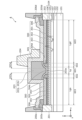
- FIG. 1 is a cross-sectional view of a semiconductor device according to a first embodiment.
- FIG. 2 is a diagram showing the relationship between the thickness of the Si 3 N 4 film and the carrier concentration of the 2DEG.
- FIG. 3 is a diagram showing the relationship between the thickness of the Si 3 N 4 film and the warpage of the wafer.
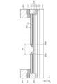
- FIG. 4 is a cross-sectional view of a semiconductor device according to the second embodiment.
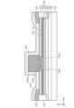
- FIG. 5 is a cross-sectional view of a semiconductor device according to a third embodiment.
- FIG. 6 is a cross-sectional view of a semiconductor device according to a fourth embodiment.
- FIG. 7 is a diagram showing the current characteristics of a semiconductor device versus the combination of the thickness of the in-situ Si 3 N 4 film and the thickness of the barrier layer.
- FIG. 8 is a cross-sectional view of a semiconductor device for supplementary explanation of the current characteristics shown in FIG.
- FIG. 9A is a cross-sectional view for explaining one step of a method for manufacturing a semiconductor device according to the third embodiment.
- FIG. 9B is a cross-sectional view for explaining one step of the method for manufacturing the semiconductor device according to the third embodiment.
- FIG. 9C is a cross-sectional view for explaining one step of the method for manufacturing a semiconductor device according to the third embodiment.
- FIG. 9A is a cross-sectional view for explaining one step of a method for manufacturing a semiconductor device according to the third embodiment.
- FIG. 9B is a cross-sectional view for explaining one step of the method for manufacturing the semiconductor device according to the third embodiment.
- FIG. 9C is a cross-sectional view for explaining
- FIG. 9D is a cross-sectional view for explaining one step of the method for manufacturing a semiconductor device according to the third embodiment.
- FIG. 9E is a cross-sectional view for illustrating a step of the method for manufacturing a semiconductor device according to the third embodiment.
- FIG. 9F is a cross-sectional view for explaining one step of the method for manufacturing a semiconductor device according to the third embodiment.
- FIG. 9G is a cross-sectional view for explaining one step of the method for manufacturing a semiconductor device according to the third embodiment.
- FIG. 9H is a cross-sectional view for illustrating one step of the method for manufacturing a semiconductor device according to the third embodiment.
- FIG. 9I is a cross-sectional view for explaining one step of the method for manufacturing the semiconductor device according to the third embodiment.
- FIG. 9J is a cross-sectional view for explaining one step of the method for manufacturing a semiconductor device according to the third embodiment.
- FIG. 9K is a cross-sectional view for explaining one step of the method for manufacturing a semiconductor device according to the third embodiment.
- FIG. 10A is a cross-sectional view for explaining one step of a method for manufacturing a semiconductor device according to the fourth embodiment.
- FIG. 10B is a cross-sectional view for explaining one step of the method for manufacturing the semiconductor device according to the fourth embodiment.
- FIG. 10C is a cross-sectional view for explaining one step of the method for manufacturing a semiconductor device according to the fourth embodiment.
- each figure is a schematic diagram and is not necessarily an exact illustration. Therefore, for example, the scales of each figure do not necessarily match.
- the same reference numerals are used for substantially the same configuration, and duplicate explanations are omitted or simplified.
- the terms “above” and “below” do not refer to the upward direction (vertically upward) and downward direction (vertically downward) in an absolute spatial sense, but are used as terms defined by a relative positional relationship based on the stacking order in a stacked configuration. Furthermore, the terms “above” and “below” are applied not only to cases where two components are arranged with a gap between them and another component exists between the two components, but also to cases where two components are arranged in close contact with each other and the two components are in contact.
- the x-axis, y-axis, and z-axis indicate the three axes of a three-dimensional orthogonal coordinate system.
- the two axes parallel to the main surface (top surface) of the substrate of the semiconductor device are the x-axis and y-axis, and the direction perpendicular to this main surface is the z-axis direction.
- the direction in which the source electrode, gate electrode, and drain electrode are arranged in this order that is, the so-called gate length direction, is the x-axis direction.
- the positive direction of the z-axis may be described as "upward” and the negative direction of the z-axis may be described as "downward".
- the source electrode side or source side both refer to the negative side (negative direction) of the x-axis
- the drain electrode side or drain side both refer to the positive side (positive direction) of the x-axis
- planar view refers to the main surface (top surface) of the substrate of the semiconductor device when viewed from the positive direction of the z-axis, unless otherwise specified.
- a group III nitride semiconductor is a semiconductor containing one or more group III elements and nitrogen.
- group III elements include aluminum (Al), gallium (Ga), and indium (In).
- group III nitride semiconductors include GaN, AlN, InN, AlGaN, InGaN, and AlInGaN.
- Group III nitride semiconductors may contain one or more elements other than group III elements, such as silicon (Si) and phosphorus (P).
- Si silicon
- P phosphorus
- a layer made of material A such as a Group III nitride semiconductor such as GaN or AlGaN, silicon nitride or silicon oxide, and a layer composed of material A, mean that the layer contains substantially only material A.
- the layer may contain other elements as impurities, such as elements that are unavoidable in the manufacturing process, at a ratio of 1 at % or less.
- the composition ratio (composition rate) of a group III element of a nitride semiconductor represents the ratio of the number of atoms of a group III element of interest among a plurality of group III elements contained in the nitride semiconductor.
- the Al composition ratio of the nitride semiconductor layer can be expressed as a/(a + b + c).
- the In composition ratio and the Ga composition ratio are expressed as b/(a + b + c) and c/(a + b + c), respectively.
- ordinal numbers such as “first” and “second” do not refer to the number or order of components, unless otherwise specified, but are used for the purpose of avoiding confusion between and distinguishing between components of the same type.
- Fig. 1 is a cross-sectional view of a semiconductor device 1 according to the first embodiment.
- the semiconductor device 1 includes a substrate 101, a buffer layer 102, a channel layer 103, and a nitride semiconductor layer 104.
- the nitride semiconductor layer 104 includes a barrier layer 105 and a cap layer 106.
- a 2DEG 107 is formed near the interface between the channel layer 103 and the barrier layer 105.
- the buffer layer 102, the channel layer 103, the barrier layer 105, and the cap layer 106 are epitaxial layers (also called epilayers) formed by epitaxial growth.
- the semiconductor device 1 also includes a source electrode 201, a drain electrode 202, a gate electrode 203, a source field plate 204, barrier metals 205s and 205d, and wiring metals 206s and 206d.
- the semiconductor device 1 also includes insulating layers 300 and 305.
- the insulating layer 300 includes an in-situ Si 3 N 4 film 301 and an ex-situ Si 3 N 4 film 302 .
- the substrate 101 is a substrate made of Si.
- the substrate 101 may be an SOI (Silicon on Insulator) substrate.
- the substrate 101 may also be a substrate made of SiC, sapphire, diamond, GaN, AlN, or the like.
- the buffer layer 102 is provided above the substrate 101.
- the buffer layer 102 is provided in contact with the upper surface of the substrate 101.
- the buffer layer 102 is, for example, a layer made of a group III nitride semiconductor.
- the buffer layer 102 is made of a multi-layer structure of AlN and AlGaN with a film thickness of 2 ⁇ m.
- the buffer layer 102 may also be made of a single layer or multiple layers of a group III nitride semiconductor such as GaN, AlGaN, AlN, InGaN, or AlInGaN.
- the buffer layer 102 By providing the buffer layer 102, it is possible to reduce adverse effects such as crystal dislocations and lattice defects caused by the difference in lattice spacing between the substrate 101 and the channel layer 103. Furthermore, even if the substrate 101 has defects, the provision of the buffer layer 102 makes it possible to suppress the effects of the defects on the channel layer 103. This reduces defects in the channel layer 103, improves crystallinity, and increases the electron mobility in the channel layer 103. Note that the buffer layer 102 does not necessarily have to be provided.
- the channel layer 103 is provided above the substrate 101. Specifically, the channel layer 103 is provided in contact with the upper surface of the buffer layer 102.
- the channel layer 103 is a layer made of a nitride semiconductor containing Ga elements.
- the channel layer 103 is made of GaN.
- the thickness of the channel layer 103 is, for example, 50 nm to 300 nm, and is 200 nm as an example.
- the channel layer 103 is not limited to GaN, and may be made of a group III nitride semiconductor such as InGaN, AlGaN, or AlInGaN.
- the channel layer 103 may contain n-type impurities.
- the thickness of the channel layer 103 is not limited to the above example.
- the barrier layer 105 is provided above the channel layer 103. Specifically, the barrier layer 105 is provided in contact with the upper surface of the channel layer 103. Note that a spacer layer made of AlN and having a film thickness of, for example, about 1 nm may be provided between the barrier layer 105 and the channel layer 103. In this way, the channel layer 103 and the barrier layer 105 do not need to be in contact with each other.
- the barrier layer 105 has a larger band gap than the channel layer 103 and is a layer made of a nitride semiconductor containing Ga elements.
- the barrier layer 105 is made of, for example, AlGaN.
- the Al composition ratio of the barrier layer 105 is, for example, 10% to 30%, but may be 20% to 30%.
- the Al composition ratio of the barrier layer 105 is, for example, 25% or less.
- the thickness of the barrier layer 105 is, for example, 7 nm to 10 nm, and is, for example, 9 nm.
- the thickness of the barrier layer 105 may be 15 nm or less, 20 nm or less, or 30 nm or less.
- the barrier layer 105 is not limited to AlGaN, and may be made of a group III nitride semiconductor such as AlInGaN.
- the barrier layer 105 may contain n-type impurities.
- the lattice spacing of the barrier layer 105 is more easily relaxed than when the barrier layer 105 is made of AlN that does not include Ga elements. This makes it possible to prevent cracks from occurring in the barrier layer 105. In addition, it is possible to prevent warping of the wafer. This makes it possible to improve the quality of the semiconductor device 1.
- a high concentration of 2DEG 107 is generated due to the piezoelectric stress of the barrier layer 105 on the channel layer 103.
- the 2DEG 107 is used as the channel of the transistor.
- the cap layer 106 contacts and covers the upper surface of the barrier layer 105.
- the cap layer 106 is a layer made of a group III nitride semiconductor.
- the cap layer 106 is made of, for example, GaN.
- the thickness of the cap layer 106 is, for example, about 1 nm or more and about 2 nm or less.
- the source electrode 201 and the drain electrode 202 are provided above the substrate 101 with a gap between them. Specifically, the source electrode 201 and the drain electrode 202 are provided facing each other with the gate electrode 203 sandwiched between them.
- the source electrode 201 and the drain electrode 202 are formed using a conductive material.
- the source electrode 201 and the drain electrode 202 are a multilayer electrode film having a laminated structure in which a Ti film and an Al film are laminated in order, but are not limited to this.
- the source electrode 201 and the drain electrode 202 may be an alloy layer formed by annealing a laminated structure of a Ti film and an Al film at a temperature of 500°C or higher.
- the source electrode 201 and the drain electrode 202 may also be a transition metal, a nitride or carbide of a transition metal.
- the source electrode 201 and the drain electrode 202 may be Ta, Hf, W, Ni, TiN, TaN, HfN, WN, TiC, TaC, HfC, Au, Cu, etc., may be a compound containing these elements, or may be a multilayer electrode film having a multiple laminated structure.
- the source electrode 201 and the drain electrode 202 are also called ohmic electrodes, and are electrically connected to the 2DEG 107 through an ohmic connection.
- the source electrode 201 and the drain electrode 202 are each provided so as to be in contact with the 2DEG 107.
- the semiconductor device 1 has two recesses that penetrate the cap layer 106 and the barrier layer 105 and reach the channel layer 103.
- the two recesses are also called a source opening and a drain opening.
- the source electrode 201 is provided so as to contact and cover the inner surface of the source opening
- the drain electrode 202 is provided so as to contact and cover the inner surface of the drain opening.
- the bottom surface of each of the two recesses is located below the interface between the channel layer 103 and the barrier layer 105. Therefore, the 2DEG 107 is exposed on the side surface of each of the two recesses.
- the source electrode 201 and the drain electrode 202 are each in contact with the 2DEG 107 on the side surface of the recess. This makes it possible to reduce the channel contact resistance.
- a source contact region and a drain contact region that have low resistance due to the addition of n-type impurities to a part of the cap layer 106, the barrier layer 105, and the channel layer 103 may be provided.
- the source and drain contact regions are formed, for example, by plasma treatment, ion implantation, and crystal regrowth.
- the source electrode 201 and the drain electrode 202 are each covered with an insulating film (specifically, the insulating layer 305 before the openings are formed) during the manufacturing process of the semiconductor device 1.
- an insulating film specifically, the insulating layer 305 before the openings are formed
- openings are provided in the insulating layer 305, and wiring metals 206s and 206d are connected to the source electrode 201 and the drain electrode 202, respectively, through the openings.
- the wiring metals 206s and 206d are formed using, for example, low-resistance Au.
- a reaction between the materials may occur in a high-temperature environment.
- a barrier metal 205s is provided between the source electrode 201 and the wiring metal 206s.
- a barrier metal 205d is provided between the drain electrode 202 and the wiring metal 206d.
- the barrier metals 205d and 205s are formed using a material containing a high-melting point metal that is unlikely to react even at high temperatures.
- the barrier metals 205d and 205s are TiN films. Note that the barrier metals 205d and 205s and the wiring metals 206d and 206s do not have to be provided.
- the source electrode 201 and the drain electrode 202 may also function as wiring.
- the gate electrode 203 is provided above the barrier layer 105, between the source electrode 201 and the drain electrode 202, and spaced apart from each other.
- the gate electrode 203 has a multi-layer structure made up of a lower gate electrode portion 203L and an upper gate electrode portion 203U.
- the gate electrode lower portion 203L is formed using a conductive material capable of forming a Schottky junction with a nitride semiconductor containing Ga element.
- the gate electrode lower portion 203L is formed using Ni, Ti, TiN, TaN, W, Pd, etc.
- the gate electrode lower portion 203L is located at the bottom layer of the multi-layered gate electrode 203, and is in contact with the cap layer 106 and the insulating layer 300.
- the thickness of the gate electrode lower portion 203L is, for example, 10 nm to 50 nm, and is 50 nm as an example, but is not limited to this.
- the upper part 203U of the gate electrode is formed using a material having a lower resistivity than the lower part 203L of the gate electrode.
- the upper part 203U of the gate electrode is formed using Au or Al.
- the upper part 203U of the gate electrode is provided so as to contact and cover the upper surface of the lower part 203L of the gate electrode.
- the thickness of the upper part 203U of the gate electrode is, for example, 450 nm or more and 650 nm or less, and is 500 nm as an example, but is not limited to this.
- the shape and size of the upper part 203U of the gate electrode are substantially the same as the shape and size of the lower part 203L of the gate electrode.
- the gate electrode 203 does not have to have a multi-layer structure, and may have a single-layer structure formed using a conductive material that can form a Schottky junction with a nitride semiconductor containing Ga elements.
- the gate electrode 203 has a so-called T-shaped gate structure. Specifically, the gate electrode 203 includes a junction 203a, a drain side extension 203d, and a source side extension 203s. The drain side extension 203d and the source side extension 203s are also called a gate field plate.
- the junction 203a forms a Schottky junction with the nitride semiconductor layer 104. Specifically, the junction 203a is the portion of the underside of the lower gate electrode portion 203L that is in contact with the cap layer 106. If the cap layer 106 is not provided, the junction 203a is the portion of the underside of the lower gate electrode portion 203L that is in contact with the barrier layer 105.
- the drain side protrusion 203d is an example of a first protrusion, and is a portion that protrudes toward the drain electrode 202 side beyond the junction 203a.
- the drain side protrusion 203d corresponds to one arm of the T in the T-shaped gate structure.
- the source side protrusion 203s is an example of a second protrusion, and is a portion that protrudes further toward the source electrode 201 than the junction 203a.
- the source side protrusion 203s corresponds to one arm of the T in the T-shaped gate structure.
- the overhang length of the drain-side overhang portion 203d is the same as the overhang length of the source-side overhang portion 203s.
- the cross-sectional shape of the gate electrode 203 in the xz cross section has a shape that is linearly symmetrical with respect to a line that passes through the center of the junction portion 203a and is parallel to the z-axis.
- the protruding length of the protruding portion is the distance along the x-axis direction from the starting point to the tip of the protruding portion.
- the starting point of the protruding portion can be regarded as the outline of the junction 203a in a planar view.
- the tip of the protruding portion is the position farthest from the starting point in the protruding direction of the protruding portion.
- the protruding direction is the positive direction of the x-axis in the case of the drain side protruding portion 203d, and is the negative direction of the x-axis in the case of the source side protruding portion 203s.
- the drain side extension 203d and the source side extension 203s each have a multi-layer structure of an upper gate electrode portion 203U and a lower gate electrode portion 203L, but are not limited to this.
- the drain side extension 203d and the source side extension 203s each may have only a low-resistance upper gate electrode portion 203U.
- the lower gate electrode portion 203L may be provided only in the portion where the gate electrode 203 and the cap layer 106 (or the barrier layer 105) contact each other (the portion corresponding to the junction portion 203a).
- the distance along the x-axis from the drain side end of junction 203a to drain electrode 202 is called gate-drain distance Lgd.
- the distance along the x-axis from the source side end of junction 203a to source electrode 201 is called gate-source distance Lgs.
- Lgs ⁇ Lgd is 3.2 ⁇ m and Lgs is 1.3 ⁇ m.
- the source field plate 204 is provided above the gate electrode 203, and is set to the same potential as the source electrode 201. Specifically, the source field plate 204 is provided above the insulating layer 305. The source field plate 204 is provided such that at least a portion of it is located between the gate electrode 203 and the drain electrode 202 in a planar view. In the example shown in FIG. 1, the source field plate 204 is arranged such that a portion of it overlaps the gate electrode 203 in a planar view. The source field plate 204 is electrically insulated from the gate electrode 203 and the drain electrode 202, and is set to the potential (source potential) applied to the source electrode 201.
- a high voltage of up to about 100V to 150V is applied to the drain electrode 202.
- a high electric field is applied between the drain electrode 202 and the gate electrode 203.
- the electric field lines from the drain electrode 202 are concentrated at the end of the drain-side overhang 203d of the gate electrode 203, increasing the peak value of the electric field and reducing reliability.
- the source field plate 204 can alleviate the high electric field peak by dispersing it in the x-axis direction. This can improve the gate-drain breakdown voltage and reliability by suppressing gate leakage current.
- the source field plate 204 is formed using a conductive material.
- the source field plate 204 is, for example, a multi-layer electrode film structure consisting of a laminated structure in which a TiN film and an Al film are laminated in order.
- the thickness of the source field plate 204 is, for example, 500 nm, but is not limited to this.
- the source field plate 204 is not limited to a laminated structure of a TiN film and an Al film, and may be a nitride or carbide of a transition metal formed by sputtering.
- the source field plate 204 may be Ti, Ta, W, Ni, TiN, TaN, WN, W, Au, Cu, etc., may be a compound containing these elements, or may be a multi-layer electrode film consisting of a plurality of laminated structures.
- the source field plate 204 has a multi-layer structure in which Ti, TiN, and Al are laminated in this order from the bottom.
- the source field plate 204 may contain Au in the top layer.
- the insulating layer 305 is provided between the gate electrode 203 and the source field plate 204. Specifically, the insulating layer 305 is provided so as to cover the entire area of the semiconductor device 1. The insulating layer 305 has openings for ensuring contact with each of the source electrode 201 and the drain electrode 202.
- the insulating layer 305 is made of, for example, Si3N4 having a thickness of 110 nm. Note that the insulating layer 305 is not limited to Si3N4 , and may be made of SiO2 or SiON. The Si3N4 constituting the insulating layer 305 may have a different Si composition rate or N composition rate to control stress. Note that the insulating layer 305 and the source field plate 204 do not necessarily have to be provided.
- the insulating layer 300 is provided above the nitride semiconductor layer 104, between the gate electrode 203 and the drain electrode 202. Specifically, the insulating layer 300 contacts and covers the upper surface of the cap layer 106 between the gate electrode 203 and the drain electrode 202. The insulating layer 300 is provided over the entire range from the drain side end of the junction 203a to the drain electrode 202.
- the insulating layer 300 is also provided between the gate electrode 203 and the source electrode 201. Specifically, the insulating layer 300 contacts and covers the upper surface of the cap layer 106 between the gate electrode 203 and the source electrode 201. The insulating layer 300 is provided over the entire range from the source side end of the junction 203a to the source electrode 201.
- the insulating layer 300 has a laminated structure of a plurality of insulating layers. Specifically, the insulating layer 300 includes an in-situ Si 3 N 4 film 301 and an ex-situ Si 3 N 4 film 302.
- the in-situ Si 3 N 4 film 301 is an example of a first insulating film made of silicon nitride, and is located between the drain side overhang 203d and the nitride semiconductor layer 104, and contacts and covers the nitride semiconductor layer 104.
- the in-situ Si 3 N 4 film 301 overlaps the drain side overhang 203d in a plan view.
- the in-situ Si 3 N 4 film 301 is the bottom layer of the insulating layer 300 having a laminated structure.
- the in-situ Si 3 N 4 film 301 contacts and covers the cap layer 106 between the gate electrode 203 and the drain electrode 202 in the entire range from the drain side end of the junction 203a to the drain electrode 202.
- the in-situ Si 3 N 4 film 301 is also provided between the gate electrode 203 and the source electrode 201.
- the in-situ Si 3 N 4 film 301 overlaps the source side protruding portion 203s in a plan view.
- the in-situ Si 3 N 4 film 301 contacts and covers the cap layer 106 in the entire range from the source side end of the junction 203a to the source electrode 201.
- the ex-situ Si 3 N 4 film 302 is an example of a second insulating film made of silicon nitride, and is located between the drain side overhang 203d and the in-situ Si 3 N 4 film 301. Specifically, the ex-situ Si 3 N 4 film 302 overlaps the drain side overhang 203d in a plan view, and is in contact with the lower surface of the drain side overhang 203d. In addition, the ex-situ Si 3 N 4 film 302 contacts and covers the in-situ Si 3 N 4 film 301 in the entire area from the drain side end of the junction 203a to the drain electrode 202.
- the ex-situ Si 3 N 4 film 302 is also provided between the gate electrode 203 and the source electrode 201. Specifically, the ex-situ Si 3 N 4 film 302 overlaps the source side overhang 203s in plan view and is in contact with the lower surface of the source side overhang 203s. The ex-situ Si 3 N 4 film 302 contacts and covers the in-situ Si 3 N 4 film 301 over the entire area from the source side end of the junction 203a to the source electrode 201.
- the thickness of the in-situ Si 3 N 4 film 301 is, for example, 15 nm or more, but may be 20 nm or more. Also, the thickness of the in-situ Si 3 N 4 film 301 is 30 nm or less, but may be 25 nm or less. In this embodiment, the thickness of the in-situ Si 3 N 4 film 301 is substantially uniform.
- the thickness of the ex-situ Si 3 N 4 film 302 is, for example, 30 nm or more and 60 nm or less. Also, for example, the thickness of the ex-situ Si 3 N 4 film 302 is equal to or more than the thickness of the in-situ Si 3 N 4 film 301. In this embodiment, the thickness of the ex-situ Si 3 N 4 film 302 is substantially uniform.
- the in-situ Si 3 N 4 film 301 and the ex-situ Si 3 N 4 film 302 are manufactured by different methods. Specifically, the in-situ Si 3 N 4 film 301 is formed continuously after epitaxial growth of a nitride semiconductor without exposure to the atmosphere. That is, the in-situ Si 3 N 4 film 301 is a film continuously laminated on a nitride semiconductor layer grown in an epitaxial growth furnace.
- the growth furnace is, for example, a MOCVD furnace (MOCVD: Metal Organic Chemical Vapor Deposition).
- the ex-situ Si 3 N 4 film 302 is formed after the in-situ Si 3 N 4 film 301 is formed, the film is removed from the epitaxial growth furnace and exposed to the atmosphere, and the ex-situ Si 3 N 4 film 302 is formed by, for example, a low-pressure chemical vapor deposition (LPCVD) method.
- LPCVD low-pressure chemical vapor deposition
- the in-situ Si 3 N 4 film 301 and the ex-situ Si 3 N 4 film 302 have different film properties.
- the in-situ Si 3 N 4 film 301 is a denser film than the ex-situ Si 3 N 4 film 302.
- the film density of the in-situ Si 3 N 4 film 301 is greater than the film density of the ex-situ Si 3 N 4 film 302.
- a difference occurs in at least one of the halogen concentration and the interface oxygen concentration between the In-situ Si 3 N 4 film 301 and the Ex-situ Si 3 N 4 film 302.
- at least one of the following is satisfied: (a) the halogen concentration of the In-situ Si 3 N 4 film 301 is lower than the halogen concentration of the Ex-situ Si 3 N 4 film 302, and (b) the interface oxygen concentration between the In-situ Si 3 N 4 film 301 and the nitride semiconductor layer 104 is lower than the interface oxygen concentration between the In-situ Si 3 N 4 film 301 and the Ex-situ Si 3 N 4 film 302.
- the halogen concentration of the in-situ Si 3 N 4 film 301 is less than 1 ⁇ 10 18 atom/cm 3 and the halogen concentration of the ex-situ Si 3 N 4 film 302 is greater than 1 ⁇ 10 18 atom/cm 3 ; and (d) the interface oxygen concentration between the in-situ Si 3 N 4 film 301 and the nitride semiconductor layer 104 is less than 1 ⁇ 10 20 atom/cm 3 and the interface oxygen concentration between the in-situ Si 3 N 4 film 301 and the ex-situ Si 3 N 4 film 302 is greater than 1 ⁇ 10 20 atom/cm 3 .
- Table 1 shows the halogen concentration and interface oxygen concentration of each of in-situ Si3N4 and ex-situ Si3N4. Specifically, the results of composition analysis of the stacked structures of in-situ Si3N4 and ex - situ Si3N4 by secondary ion mass spectroscopy (SIMS) are shown. Specifically, the halogen concentration is the chlorine (Cl) concentration .
- the in-situ Si 3 N 4 film 301 is characterized by a low halogen concentration and a low oxygen concentration at the interface with the epitaxially grown semiconductor (the cap layer 106 in this embodiment). This is because the film is a laminated film in an epitaxial growth furnace and is not exposed to air, so halogens such as Cl 2 and oxygen contained in the outside air of the process site in the clean room are not easily absorbed after epitaxial growth. Cl 2 is used as a dry etching gas in the process step, and a small amount of it unintentionally enters the atmosphere.
- the effect obtained from the in-situ Si 3 N 4 film 301 having a small amount of impurities such as halogen or oxygen is that the interface state with the semiconductor is reduced, and the influence on the 2DEG 107 is reduced.
- these effects also result in an effect of high collapse resistance.
- the in-situ Si 3 N 4 film 301 is provided on the nitride semiconductor layer 104, good collapse characteristics are realized, and high drive current characteristics can be obtained.
- Fig. 2 is a diagram showing the relationship between the film thickness of the Si 3 N 4 film and the carrier concentration of the 2DEG 107.
- Fig. 2 shows a case where an in-situ Si 3 N 4 film is formed on the nitride semiconductor layer 104 (Example) and a case where an ex-situ Si 3 N 4 film is formed on the nitride semiconductor layer 104 (Comparative Example).
- the horizontal axis represents the film thickness of the Si 3 N 4 film
- the vertical axis represents the carrier concentration of the 2DEG 107 obtained by Hall measurement.
- the in-situ Si3N4 film has a significantly higher carrier concentration than the ex-situ Si3N4 film , and therefore the saturation current of the transistor is higher.
- the higher the saturation current the higher the high-output and gain characteristics of the transistor.
- Figure 3 is a diagram showing the relationship between the thickness of the Si 3 N 4 film and the warpage of the wafer.
- the horizontal axis represents the thickness of the Si 3 N 4 film
- the vertical axis represents the amount of warpage of the wafer. Note that Figure 3 shows the measurement results for a 6-inch wafer.
- both the in-situ Si 3 N 4 film and the ex-situ Si 3 N 4 film have a tendency that the warpage of the wafer increases as the film thickness increases.
- the quality of the semiconductor device 1 deteriorates, such as cracks occurring at the outer periphery of the wafer.
- an upper limit for the film thickness of the Si 3 N 4 film provided on the nitride semiconductor layer 104.
- the critical film thickness of the in-situ Si 3 N 4 film is 25 nm.
- the amount of warpage when an in-situ Si 3 N 4 film is provided is larger than the amount of warpage when an ex-situ Si 3 N 4 film is provided.
- an ex-situ Si 3 N 4 film is more advantageous than an in-situ Si 3 N 4 film.
- the insulating layer 300 provided on the nitride semiconductor layer 104 has a laminated structure of an in-situ Si 3 N 4 film 301 and an ex-situ Si 3 N 4 film 302.
- the provision of the ex-situ Si 3 N 4 film 302 increases the piezoelectric stress, and the electron carrier concentration of the 2DEG 107 can be increased.
- the saturation current of the transistor can be increased. Note that the saturation current is determined by the saturation velocity of electrons, and therefore depends more on the electron carrier concentration than on the mobility, which has a large effect at low voltages. In this way, according to this embodiment, high drive current characteristics and low wafer warpage characteristics can be realized.
- the thickness of the ex-situ Si3N4 film also has an upper limit (critical film thickness). Specifically, the critical film thickness of the ex-situ Si3N4 film is 60 nm.
- the critical film thickness of the ex-situ Si3N4 film is 60 nm.
- the following formula (1) is satisfied when the film thickness of the in- situ Si3N4 film 301 is Tin and the film thickness of the ex-situ Si3N4 film 302 is Tex .
- f(T in ) is a function expressing the relationship between the film thickness T in of the in-situ Si 3 N 4 film 301 and the amount of wafer warpage.
- g(T ex ) is a function expressing the relationship between the film thickness T in of the ex-situ Si 3 N 4 film 302 and the amount of wafer warpage.
- T in is 25 nm or less, and T ex is 60 nm or less.
- the in-situ Si 3 N 4 film 301 is effective against the collapse phenomenon.
- the effect of the ex-situ Si 3 N 4 film 302, which is additionally stacked, on the collapse phenomenon will be described below.
- the In-situ Si 3 N 4 film 301 has a certain amount of impurity levels, although the amount is less than that of the Ex-situ Si 3 N 4 film 302. Therefore, there is a risk that electrons are captured in the impurity levels of the In-situ Si 3 N 4 film 301.
- the electrons captured in the impurity levels of the In-situ Si 3 N 4 film 301 can be conducted through the leak path of the Ex-situ Si 3 N 4 film 302 laminated on the In-situ Si 3 N 4 film 301.
- the laminated structure is more effective in suppressing the collapse phenomenon than providing the In-situ Si 3 N 4 film 301 alone, and the driving current characteristics can be improved.
- the ex-situ Si 3 N 4 film 302 is provided directly on the epitaxial surface, the leakage current becomes too large to be ignored. Therefore, by providing the in-situ Si 3 N 4 film 301 so as to cover the epitaxial surface, and providing the ex-situ Si 3 N 4 film 302 on the in-situ Si 3 N 4 film 301, it is possible to realize high drive current characteristics and low wafer warpage characteristics.
- Embodiment 2 Next, a description will be given of embodiment 2.
- a SiO 2 film is provided on an ex-situ Si 3 N 4 film, which is a main difference from embodiment 1.
- the description will be centered on the differences from embodiment 1, and the description of the commonalities will be omitted or simplified.
- Fig. 4 is a cross-sectional view of the semiconductor device 2 according to the present embodiment. As shown in Fig. 4, the semiconductor device 2 is different from the semiconductor device 1 shown in Fig. 1 in that the insulating layer 300 further includes a SiO2 film 303.
- the SiO 2 film 303 is an example of a third insulating film made of silicon oxide, and is located between the drain side extension 203d and the ex-situ Si 3 N 4 film 302.
- the SiO 2 film 303 is the top layer of the insulating layer 300 having a laminated structure.
- the SiO 2 film 303 is in contact with the drain side extension 203d.
- the SiO 2 film 303 overlaps the drain side extension 203d in a plan view and is in contact with the lower surface of the drain side extension 203d.
- the SiO 2 film 303 contacts and covers the ex -situ Si 3 N 4 film 302 between the gate electrode 203 and the drain electrode 202 in the entire range from the drain side end of the junction 203a to the drain electrode 202.
- the SiO 2 film 303 is also provided between the gate electrode 203 and the source electrode 201. Specifically, the SiO 2 film 303 overlaps the source side overhang 203s in a plan view and is in contact with the lower surface of the source side overhang 203s. The SiO 2 film 303 contacts and covers the ex-situ Si 3 N 4 film 302 in the entire area from the source side end of the junction 203a to the source electrode 201.
- the thickness of the SiO 2 film 303 is, for example, 10 nm to 100 nm, for example, 50 nm. In this embodiment, the thickness of the SiO 2 film 303 is substantially uniform.
- the relative dielectric constant of Si 3 N 4 is about 7, while the relative dielectric constant of SiO 2 is about 4. That is, the SiO 2 film 303 has a lower dielectric constant than both the in-situ Si 3 N 4 film 301 and the ex-situ Si 3 N 4 film 302. Therefore, by providing the SiO 2 film 303 between the drain side overhang 203d and the 2DEG 107, the gate-drain capacitance Cgd can be reduced. By reducing the gate-drain capacitance Cgd, the high frequency gain characteristics and efficiency performance of the transistor can be improved.
- the third embodiment is mainly different from the first embodiment in that a sidewall structure is provided at the gate portion.
- the following description will focus on the differences from the first embodiment, and the description of the commonalities will be omitted or simplified.
- Fig. 5 is a cross-sectional view of the semiconductor device 3 according to the present embodiment. As shown in Fig. 5, the semiconductor device 3 is different from the semiconductor device 1 shown in Fig. 1 in that the insulating layer 300 further includes side walls 304d and 304s and an ex-situ Si 3 N 4 film 306.
- the sidewall 304d is provided between the junction 203a of the gate electrode 203 and the In-situ Si 3 N 4 film 301. Specifically, the sidewall 304d is a drain-side sidewall, and is provided between the junction 203a and a portion of the In-situ Si 3 N 4 film 301 on the drain electrode 202 side.
- the sidewall 304s is provided between the junction 203a of the gate electrode 203 and the In-situ Si 3 N 4 film 301.
- the sidewall 304s is a source sidewall, and is provided between the junction 203a and a portion of the In-situ Si 3 N 4 film 301 on the source electrode 201 side.
- Both the sidewalls 304d and 304s are made of silicon nitride. More specifically, the sidewalls 304d and 304s are made of ex-situ Si 3 N 4 and are formed in the same process.
- each of the sidewalls 304d and 304s is different from that of the ex-situ Si 3 N 4 film 302.
- the sidewalls 304d and 304s are films that are less dense than the ex-situ Si 3 N 4 film 302.
- the film density of each of the sidewalls 304d and 304s is smaller than that of the ex-situ Si 3 N 4 film 302.
- the sidewalls 304d and 304s are formed in a process different from that of the ex-situ Si 3 N 4 film 302. A specific formation method will be described later.
- the ex-situ Si 3 N 4 film 306 is provided above the ex-situ Si 3 N 4 film 302. Specifically, the ex-situ Si 3 N 4 film 306 is provided at a position not overlapping the drain side protruding portion 203d of the gate electrode 203 in a plan view. More specifically, the ex-situ Si 3 N 4 film 306 is provided so as to be in contact with the drain electrode 202.
- the ex-situ Si 3 N 4 film 306 is also provided on the source electrode 201 side. Specifically, the ex-situ Si 3 N 4 film 306 is provided at a position not overlapping the source side protruding portion 203s of the gate electrode 203. More specifically, the ex-situ Si 3 N 4 film 306 is provided so as to be in contact with the source electrode 201.
- the film quality of the ex-situ Si 3 N 4 film 306 is different from that of the ex-situ Si 3 N 4 film 302.
- the ex-situ Si 3 N 4 film 306 is a film that is sparser than the ex-situ Si 3 N 4 film 302.
- the film density of the ex-situ Si 3 N 4 film 306 is smaller than that of the ex-situ Si 3 N 4 film 302.
- the ex-situ Si 3 N 4 film 306 can be formed in the same process as the sidewalls 304d and 304s.
- the insulating layer 300 has a larger thickness in the vicinity of the drain electrode 202 than in the vicinity of the gate electrode 203. Directly below the portion with the larger thickness, that is, directly below the ex-situ Si 3 N 4 film 306, more electric charges are generated by piezoelectric polarization. Therefore, the carrier concentration of the 2DEG 107 increases directly below the ex-situ Si 3 N 4 film 306. Since the ex-situ Si 3 N 4 film 306 is provided so as to contact the drain electrode 202, the carrier concentration of the portion of the 2DEG 107 that contacts the drain electrode 202 increases. Therefore, the contact resistance between the drain electrode 202 and the 2DEG 107 can be reduced. Therefore, the on-resistance is reduced, and high drive current characteristics can be obtained.
- the ex-situ Si 3 N 4 film 306 is provided so as to be in contact with the source electrode 201, it is possible to reduce the contact resistance between the source electrode 201 and the 2DEG 107. As a result, the on-resistance is reduced, and high drive current characteristics can be obtained.
- the ex-situ Si 3 N 4 film 306 may be formed in a process different from that for the side walls 304d and 304s.
- the film quality of the ex-situ Si 3 N 4 film 306 may be the same as that of the ex-situ Si 3 N 4 film 302.
- the ex-situ Si 3 N 4 film 306 may be a film denser than the ex-situ Si 3 N 4 film 302.
- the ex-situ Si 3 N 4 film 306 may not be provided.
- the sidewalls 304d and 304s are formed using ex-situ Si 3 N 4 , a difference occurs in at least one of the halogen concentration and the interface oxygen concentration between the in-situ Si 3 N 4 film 301 and the sidewalls 304d and 304s.
- At least one of the following is satisfied: (a) the halogen concentration of the in-situ Si 3 N 4 film 301 is lower than the halogen concentration of the sidewalls 304d and 304s, and (b) the interface oxygen concentration between the in-situ Si 3 N 4 film 301 and the nitride semiconductor layer 104 is lower than the interface oxygen concentration between the sidewalls 304d and 304s and the nitride semiconductor layer 104.
- the halogen concentration of the in-situ Si 3 N 4 film 301 is less than 1 ⁇ 10 18 atom/cm 3 , and the halogen concentration of the sidewalls 304d and 304s is greater than 1 ⁇ 10 18 atom/cm 3 ; and (d) the interface oxygen concentration between the in-situ Si 3 N 4 film 301 and the nitride semiconductor layer 104 is less than 1 ⁇ 10 20 atom/cm 3 , and the interface oxygen concentration between the sidewalls 304d and 304s and the nitride semiconductor layer 104 is greater than 1 ⁇ 10 20 atom/cm 3.
- the same relationship is also satisfied between the ex-situ Si 3 N 4 film 306 and the in-situ Si 3 N 4 film 301.
- the width of the gate opening corresponds to the gate length Lg by removing a part of the in-situ Si 3 N 4 film 301 and the ex-situ Si 3 N 4 film 302. For this reason, it is not possible to realize a gate length Lg smaller than the minimum value of the processing limit of the gate opening.
- the gate length Lg can be shortened by providing the sidewalls 304d and 304s.
- the gate length Lg can be set to 0.25 ⁇ m or less.
- the gate length Lg is the length of the junction 203a along the arrangement direction (x-axis direction) of the source electrode 201, the gate electrode 203 (specifically the junction 203a), and the drain electrode 202.
- the length of each of the sidewalls 304d and 304s in the x-axis direction can be set to 0.10 ⁇ m, and Lg can be set to 0.19 ⁇ m.
- the gate length Lg can be shortened to about half the width of the gate opening, which is 0.39 ⁇ m.
- the fourth embodiment is mainly different from the third embodiment in that a SiO2 film is provided on an ex-situ Si3N4 film .
- the fourth embodiment is mainly different from the second embodiment in that a sidewall structure is provided on the gate portion. The following description will focus on the differences with the second or third embodiment, and the description of the commonalities will be omitted or simplified.
- Fig. 6 is a cross-sectional view of a semiconductor device 4 according to the present embodiment. As shown in Fig. 6, the semiconductor device 4 is different from the semiconductor device 3 shown in Fig. 5 in that the insulating layer 300 further includes a SiO2 film 303.
- the SiO 2 film 303 is the same as the SiO 2 film 303 included in the insulating layer 300 of the semiconductor device 2 according to the second embodiment. Therefore, according to the semiconductor device 4 according to the present embodiment, as in the second embodiment, the gate-drain capacitance Cgd can be reduced, and high-frequency gain characteristics and efficiency performance can be improved. Specifically, this is useful when handling signals in a frequency band of 5 GHz or more.
- the semiconductor device 4 according to this embodiment has the sidewalls 304d and 304s made of ex-situ Si 3 N 4 , similarly to the third embodiment. Therefore, the current cutoff (pinch-off) characteristics during modulation of the gate electrode 203 are improved.
- Fig. 7 is a diagram showing the current characteristics of the semiconductor device 4 for combinations of the thickness Tin of the In-situ Si 3 N 4 film 301 and the thickness Tba of the barrier layer 105.
- Fig. 8 is a cross-sectional view of the semiconductor device 4 for supplementary explanation of the current characteristics shown in Fig. 7.
- the gate length Lg of each prototype (sample) was set to 0.25 ⁇ m.
- the barrier layer 105 was an Al x Ga 1-x N film, and the Al composition ratio x was set to 0.28.
- the saturation current was a value obtained by measuring the current flowing from the drain electrode 202 to the source electrode 201 when the drain voltage applied between the drain electrode 202 and the source electrode 201 was 5 V.
- the leakage current was a value obtained by measuring the leakage current flowing from the drain electrode 202 to the gate electrode 203 when the potential difference between the drain electrode 202 and the gate electrode 203 was 150 V.
- the gate-drain distance Lgd was set to 3 ⁇ m. The longer Lgd is, the more the electric field concentration is alleviated, so the leakage current decreases, but there is a problem that the on-resistance increases.
- the saturation current When applying the semiconductor device 4 to a power amplifier, it is desirable for the saturation current to be high and the leakage current to be low.
- a semiconductor device with a saturation current of 920 mA/mm or more and a leakage current of 10 ⁇ A/mm or less is suitable for a power amplifier.
- Region 601 is a region directly below junction 203a, which is the contact surface between gate electrode 203 and nitride semiconductor layer 104.
- the thinner the barrier layer 105 is the weaker the piezoelectric stress of the barrier layer 105 against channel layer 103 will be. As a result, leakage current can also be suppressed.
- the barrier layer 105 is thinned even in the gate-drain region 603, which is the main region through which electron carriers travel, a high saturation current cannot be expected in this state. Therefore, in the present disclosure, an in-situ Si 3 N 4 film 301 is laminated on the thinned barrier layer 105 in the region 603. By utilizing the high piezoelectric stress of the in-situ Si 3 N 4 film 301, the carrier concentration of the 2DEG 107 can be increased, and the drain current can be increased.
- ex-situ Si 3 N 4 with a low stress is provided as the sidewalls 304s and 304d of the region 602.
- the piezoelectric effect can be weakened in the region 602, making it possible to cut off a high drain current.
- the barrier layer 105, the in-situ Si 3 N 4 film 301, the ex-situ Si 3 N 4 film 302, and the sidewalls 304s and 304d realize a structure in which the advantages and disadvantages of each film are complemented.
- This makes it possible to achieve both a high saturation current and a low leakage current, which have been contradictory in the past, and to realize low wafer warpage.
- the semiconductor device 4 of the present embodiment it is possible to provide a GaN HEMT having high performance and high reliability with a small leakage current. Note that although the semiconductor device 4 is given as an example, the same is true for the semiconductor devices 1 to 3 of the first to third embodiments.
- the thickness T in of the in-situ Si 3 N 4 film 301 must be 7 nm or more. From the viewpoint of wafer warpage, the thickness T in must be 25 nm or less. From the viewpoint of a leakage current of 10 ⁇ A/mm or less, the thickness T ba of the barrier layer 105 must be 10 nm or less.
- the thickness T in of the in-situ Si 3 N 4 film 301 may be smaller than 10 nm, or may be larger than 25 nm.
- the thickness T ba of the barrier layer 105 may be larger than 10 nm, or may be smaller than 7 nm.
- the method for manufacturing the semiconductor devices 1 to 4 includes a first step of forming the channel layer 103 and the nitride semiconductor layer 104 including the barrier layer 105 in this order above the substrate 101 by epitaxial growth; a second step of forming an insulating layer 300 so as to cover the nitride semiconductor layer 104; a third step of removing a part of the insulating layer 300 to expose a part of the nitride semiconductor layer 104; a fourth step of forming a source electrode 201 and a drain electrode 202 spaced apart from each other above the substrate 101; and a fifth step of forming a gate electrode 203 spaced apart from each other between the source electrode 201 and the drain electrode 202 so as to contact the exposed part of the nitride semiconductor layer 104 and cover the part of the insulating layer 300 located closer to the drain electrode 202 than the exposed part.
- the second process includes, after the first process, a process of forming an in-situ Si 3 N 4 film 301 that contacts and covers the nitride semiconductor layer 104 without exposing it to the atmosphere, and a process of forming the in-situ Si 3 N 4 film 301, and then exposing it to the atmosphere, and then forming an ex-situ Si 3 N 4 film 302 above the in-situ Si 3 N 4 film 301.
- FIG. 9A to 9K is a cross-sectional view for explaining one step of the method for manufacturing a semiconductor device 3 according to the third embodiment.
- the manufacturing method of semiconductor device 3 described below is the core of the manufacturing methods of semiconductor devices 1, 2, and 4 according to other embodiments.
- Each of the manufacturing methods of semiconductor devices 1, 2, and 4 can be easily manufactured by simply omitting or modifying a part of the manufacturing method of semiconductor device 3 described below.
- a GaN wafer is prepared by epitaxially growing a nitride semiconductor. More specifically, a buffer layer 102, a channel layer 103, a barrier layer 105, and a cap layer 106 are formed in this order on a substrate 101. For example, nitride semiconductors such as GaN and AlGaN are epitaxially grown in this order. The epitaxial growth is performed in a growth furnace based on the MOCVD method, for example. By adjusting the type and flow rate of the introduced gas, the buffer layer 102, the channel layer 103, the barrier layer 105, and the cap layer 106 can be formed.
- an in-situ Si 3 N 4 film 301 is formed. Specifically, after the epitaxial growth of the nitride semiconductor, silicon nitride is epitaxially grown in the same growth furnace without exposure to the atmosphere. This allows the in-situ Si 3 N 4 film 301 covering the upper surface of the cap layer 106 to be formed. Since the upper surface of the cap layer 106 (nitride semiconductor layer 104) is not exposed to the atmosphere, the oxygen concentration at the interface between the in-situ Si 3 N 4 film 301 and the cap layer 106 is reduced. In addition, the halogen concentration in the in-situ Si 3 N 4 film 301 is reduced.
- an ex-situ Si 3 N 4 film 302 is formed on the in-situ Si 3 N 4 film 301.
- the GaN wafer on which the in-situ Si 3 N 4 film 301 is formed is taken out of the growth furnace, and the GaN wafer is exposed to the atmosphere.
- the surface of the GaN wafer after the exposure to the atmosphere, that is, the upper surface of the in-situ Si 3 N 4 film 301, is washed with an acid such as hydrofluoric acid, and then the ex-situ Si 3 N 4 film 302 is formed.
- the ex-situ Si 3 N 4 film 302 is formed, for example, by a low pressure CVD (LPCVD: Low Pressure Chemical Vapor Deposition) method.
- LPCVD Low Pressure Chemical Vapor Deposition
- the film forming temperature in the LPCVD method is about 800° C. Therefore, the film density of the ex-situ Si 3 N 4 film 302 formed by the LPCVD method is lower than that of the in-situ Si 3 N 4 film 301, but is higher in density than the Si 3 N 4 film formed by the plasma CVD method deposited at a temperature of about 300° C. to 500° C. Therefore, the ex-situ Si 3 N 4 film 302 has an intermediate stress. Therefore, the in-situ Si 3 N 4 film 301 has a critical film thickness due to the warpage of the wafer, and is therefore more useful as a film that compensates for the piezoelectric stress. It goes without saying that the ex-situ Si 3 N 4 film 302 may be a Si 3 N 4 film formed by normal plasma CVD.
- ions that passivate nitride semiconductors such as boron ions (B + ) are implanted to passivate areas other than the transistor formation area (also called the active area), thereby enabling insulation isolation between elements within the GaN wafer.
- B + boron ions
- source electrode 201 and drain electrode 202 are formed.
- Figure 9C to 9K only show one transistor formation region in the GaN wafer.
- a part of each of the ex-situ Si 3 N 4 film 302 and the in-situ Si 3 N 4 film 301 is removed by etching to form an opening (contact hole). Furthermore, continuously from the formation of the contact hole, the cap layer 106, the barrier layer 105, and the channel layer 103 are removed by etching until the 2DEG 107 is exposed, thereby forming a recess.
- the etching is performed, for example, by dry etching.
- the metal film is patterned to form the source electrode 201 and the drain electrode 202.
- the patterning is performed, for example, by etching or lift-off.
- the semiconductor and the metal are alloyed at a temperature of about 500° C. to 600° C., so that each of the source electrode 201 and the drain electrode 202 is brought into ohmic contact with the channel layer 103.
- a gate opening is formed in the gate region 401 for forming a gate.
- the length of the gate region 401 in the x-axis direction is, for example, 0.39 ⁇ m.
- a positive photoresist is applied onto the ex-situ Si 3 N 4 film 302, and the gate region 401 of the applied photoresist is opened.
- plasma ions containing CF 4 By performing dry etching with plasma ions containing CF 4 , the portions of the ex-situ Si 3 N 4 film 302 and the in-situ Si 3 N 4 film 301 exposed in the gate region 401 are removed.
- an ex-situ Si 3 N 4 film 307 is formed on the entire surface including the opening of the gate region 401.
- the ex-situ Si 3 N 4 film 307 is formed by, for example, a plasma CVD method, but may be formed by an LPCVD method.
- the ex-situ Si 3 N 4 film 307 is a silicon nitride film that is the basis of the side walls 304s and 304d and the ex-situ Si 3 N 4 film 306.
- the ex-situ Si 3 N 4 film 307 is formed to the same thickness as the total thickness of the in-situ Si 3 N 4 film 301 and the ex-situ Si 3 N 4 film 302.
- the thickness of the ex-situ Si 3 N 4 film 307 is set to 50 nm.
- the heights of the sidewalls 304s and 304d and the heights (total thicknesses) of the in-situ Si 3 N 4 film 301 and the ex-situ Si 3 N 4 film 302 can be made uniform.
- a photoresist 501 having an opening of a predetermined shape is formed, and then anisotropic dry etching is performed with plasma ions mainly containing CF4 to remove the ex-situ Si3N4 film 307 exposed in the opening of the photoresist 501.
- the photoresist 501 has a shape that covers the source electrode 201 and the drain electrode 202, and does not cover at least the gate region 401.
- the etching amount is the thickness of the deposited ex-situ Si3N4 film 307, and is, for example, 50 nm.
- the photoresist 501 is a positive type, but may be a negative type.
- sidewalls 304s and 304d are formed by the anisotropic etching.
- the sidewalls 304s and 304d are the portions of the ex-situ Si 3 N 4 film 307 that are not removed and remain along the opening walls in the gate region 401.
- the shape of the upper surface of the sidewalls 304s and 304d is a shape transferred from the shape of the upper surface of the ex-situ Si 3 N 4 film 307. This shape is generally called the sidewall shape.
- the sidewall shape By forming the sidewalls 304s and 304d in the gate region 401, the length of the exposed part of the nitride semiconductor layer 104 in the gate region 401 (so-called gate length Lg) is shortened. Specifically, the gate length Lg is shortened from 0.39 ⁇ m to 0.19 ⁇ m.
- the length of the gate region 401 is 0.4 ⁇ m, it is possible to form a gate opening using i-line photolithography, which is a common optical exposure method. On the other hand, it is difficult to form a gate opening with a length of 0.25 ⁇ m or less. In contrast, by forming sidewalls 304s and 304d, it is possible to easily shorten the gate length Lg.
- the photoresist 501 is removed with an organic solvent such as acetone, thereby leaving a part of the ex-situ Si 3 N 4 film 307 covering the source electrode 201 and the drain electrode 202.
- the gate electrode 203 is formed. Specifically, a first conductive film made of a material that forms a Schottky junction with the nitride semiconductor is formed as the lower gate electrode portion 203L, and a second conductive film made of a material with a lower resistivity than the first conductive film is formed as the upper gate electrode portion 203U.
- the first conductive film and the second conductive film may be successively formed on the entire surface by sputtering or the like, and then a resist mask may be formed and unnecessary portions may be removed by dry etching.
- the gate electrode 203 may be formed by a lift-off method.
- the first conductive film and the second conductive film may be successively evaporated, and the resist film may be removed together with the first conductive film and the second conductive film provided on the resist film.
- the thicker the gate electrode upper portion 203U the more the gate resistance Rg can be reduced. However, due to the skin effect of metal, current flows only on the surface (skin portion) at high frequencies. Therefore, the thicker the gate electrode upper portion 203U, the better. In the case of the gate electrode upper portion 203U made of Al, a thickness of about 450 nm is sufficient to accommodate the currently used frequency band. In addition, the thickening of the gate electrode upper portion 203U may be subject to restrictions such as the film formation time, etching time, and the film thickness of the photoresist mask.
- the film thickness of the gate electrode upper portion 203U is set to about 650 nm at most.
- an insulating layer 305 is formed for the purpose of protecting the gate electrode 203.
- an ex-situ Si 3 N 4 film is formed by plasma CVD or LPCVD.
- the source field plate 204 is formed.
- the source field plate 204 is formed by depositing a metal film by sputtering and removing it by dry etching.
- the source field plate 204 may be formed by a deposition lift-off method. When using Au, the deposition lift-off method is used because dry etching is not possible.
- openings are formed in the insulating layer 305 and the ex-situ Si 3 N 4 film 307.
- the openings are formed by forming a photoresist having openings so as to expose the source electrode 201 and the drain electrode 202, and then dry etching with plasma ions containing CF 4.
- the ex-situ Si 3 N 4 film 307 having openings for contacting the source electrode 201 and the drain electrode 202 becomes the ex-situ Si 3 N 4 film 306 shown in FIG. 5.
- barrier metals 205s and 205d and wiring metals 206s and 206d of a predetermined shape are formed so as to cover the openings.
- the barrier metals 205s and 205d and the wiring metals 206s and 206d are formed by sputtering and dry etching, or a deposition lift method, or the like.
- the semiconductor device 3 shown in Figure 5 can be manufactured.
- the process of forming the sidewalls 304s and 304d can be omitted. Specifically, the processes described with reference to FIG. 9E to FIG. 9H can be omitted. After forming the gate region 401 as shown in FIG. 9D, the gate electrode 203 can be formed as shown in FIG. 9J.
- the semiconductor device 2 or 4 according to the second or fourth embodiment can be manufactured through steps substantially similar to those of the manufacturing method of the semiconductor device 3.
- the differences between the manufacturing method of the semiconductor device 3 and the manufacturing method of the semiconductor device 4 will be explained using Figures 10A to 10C.
- Figures 10A to 10C is a cross-sectional view for explaining one step of the manufacturing method of the semiconductor device 4 according to the fourth embodiment.
- the process up to the formation of the In-situ Si 3 N 4 film 301 is the same as that of the manufacturing method of the semiconductor device 3, as described with reference to FIG. 9A.
- the Ex-situ Si 3 N 4 film 302 and the SiO 2 film 303 are formed on the In-situ Si 3 N 4 film 301.
- the GaN wafer on which the In-situ Si 3 N 4 film 301 is formed is taken out of the growth furnace, and the GaN wafer is exposed to the atmosphere.
- the Ex-situ Si 3 N 4 film 302 and the SiO 2 film 303 are successively formed.
- the ex-situ Si 3 N 4 film 302 and the SiO 2 film 303 are formed by, for example, a plasma CVD method.
- the ex-situ Si 3 N 4 film 302 may be formed by an LPCVD method, and the SiO 2 film 303 may be formed by a plasma CVD method.
- the source electrode 201 and the drain electrode 202 are formed. Note that before the source electrode 201 and the drain electrode 202 are formed, a process is performed to inactivate the areas other than the transistor formation area.
- the difference is that in the process of forming the source electrode 201 and the drain electrode 202, in order to form contact holes, not only the ex-situ Si 3 N 4 film 302 and the in-situ Si 3 N 4 film 301 but also a part of the SiO 2 film 303 are removed.
- the formation and patterning of the metal film, as well as the alloying and other processes are the same as in the manufacturing method of the semiconductor device 3.
- a gate opening is formed in a gate region 401 for forming a gate.
- the difference is that the gate opening is formed by removing not only the ex-situ Si 3 N 4 film 302 and the in-situ Si 3 N 4 film 301 but also a part of the SiO 2 film 303.
- the SiO 2 film 303 is removed by dry etching using, for example, CF 4 gas.
- the process of forming the sidewalls 304s and 304d can be omitted. Specifically, the processes described with reference to FIG. 9E to FIG. 9H can be omitted. After forming the gate region 401 as shown in FIG. 10C, the gate electrode 203 can be formed as shown in FIG. 9J.
- the semiconductor device includes a substrate, a channel layer made of a nitride semiconductor containing Ga element provided above the substrate, a nitride semiconductor layer provided above the channel layer, the nitride semiconductor layer including a barrier layer having a larger band gap than the channel layer and containing Ga element, a source electrode and a drain electrode provided above the substrate with a gap therebetween, a gate electrode provided above the barrier layer between the source electrode and the drain electrode with a gap therebetween, and an insulating layer provided above the nitride semiconductor layer between the gate electrode and the drain electrode, the gate electrode being made of the nitride semiconductor layer.
- the insulating layer includes a junction portion that is a Schottky junction with the nitride semiconductor layer, and a first protruding portion that protrudes toward the drain electrode side beyond the junction portion, and the insulating layer includes a first insulating film that is located between the first protruding portion and the nitride semiconductor layer and is made of silicon nitride and that contacts and covers the nitride semiconductor layer, and a second insulating film that is located between the first protruding portion and the first insulating film and is made of silicon nitride, and at least one of the following is satisfied: (a) the halogen concentration of the first insulating film is lower than the halogen concentration of the second insulating film, and (b) the interface oxygen concentration between the first insulating film and the nitride semiconductor layer is lower than the interface oxygen concentration between the second insulating film and the first insulating film.
- a semiconductor device is the semiconductor device according to the first aspect, which satisfies at least one of the following: (c) a halogen concentration of the first insulating film is less than 1 ⁇ 10 atom/cm 3 and a halogen concentration of the second insulating film is greater than 1 ⁇ 10 atom/cm 3 ; and (d) an oxygen concentration at the interface between the first insulating film and the nitride semiconductor layer is less than 1 ⁇ 10 atom/cm 3 and a oxygen concentration at the interface between the second insulating film and the first insulating film is greater than 1 ⁇ 10 atom/cm 3 .
- the in-situ Si 3 N 4 film is provided as the first insulating film and the ex-situ Si 3 N 4 film is provided as the second insulating film, it is possible to effectively utilize the wafer warpage suppression effect of the ex-situ Si 3 N 4 film while utilizing the high piezoelectric stress of the in-situ Si 3 N 4 film.
- the semiconductor device according to the third aspect of the present disclosure is the semiconductor device according to the first or second aspect, in which the insulating layer further includes a third insulating film made of silicon oxide, located between the first protruding portion and the second insulating film, and in contact with the first protruding portion.
- the gate-drain capacitance Cgd can be reduced by the third insulating film made of silicon oxide, which has a low dielectric constant. This improves the high-frequency gain characteristics and efficiency performance of the transistor.
- the semiconductor device according to the fourth aspect of the present disclosure is a semiconductor device according to any one of the first to third aspects, in which the thickness of the first insulating film is 10 nm or more, and the thickness of the barrier layer is 7 nm or more.
- the semiconductor device according to the fifth aspect of the present disclosure is the semiconductor device according to the fourth aspect, in which the thickness of the barrier layer is 10 nm or less.
- the semiconductor device according to the sixth aspect of the present disclosure is the semiconductor device according to the fourth or fifth aspect, in which the thickness of the first insulating film is 25 nm or less.
- the semiconductor device is a semiconductor device according to any one of the first to sixth aspects, in which the insulating layer further includes a sidewall made of silicon nitride provided between the junction and the first insulating film, and satisfies at least one of the following: (e) the halogen concentration of the first insulating film is lower than the halogen concentration of the sidewall, and (f) the interface oxygen concentration between the first insulating film and the nitride semiconductor layer is lower than the interface oxygen concentration between the sidewall and the nitride semiconductor layer.
- the semiconductor device according to the eighth aspect of the present disclosure is the semiconductor device according to the seventh aspect, in which the sidewall has a film quality different from that of the second insulating film.
- a method for manufacturing a semiconductor device includes a first step of forming, by epitaxial growth, above a substrate, a channel layer made of a nitride semiconductor containing Ga, and a nitride semiconductor layer including a barrier layer having a larger band gap than the channel layer and containing Ga; a second step of forming an insulating layer to cover the nitride semiconductor layer; a third step of removing a portion of the insulating layer to expose a portion of the nitride semiconductor layer; and a fourth step of forming a source electrode and a drain electrode spaced apart from each other above the substrate.
- the second step includes, after the first step, forming a first insulating film made of silicon nitride that contacts and covers the nitride semiconductor layer without exposure to the atmosphere, and forming a second insulating film made of silicon nitride above the first insulating film after forming the first insulating film and exposing it to the atmosphere.
- the method for manufacturing a semiconductor device according to the tenth aspect of the present disclosure is the method for manufacturing a semiconductor device according to the ninth aspect, in which in the second step, the second insulating film is formed by the LPCVD method.
- the insulating layer 300 may not be provided between the source electrode 201 and the gate electrode 203.
- the in-situ Si 3 N 4 film 301 may be provided between the source electrode 201 and the gate electrode 203, and the ex-situ Si 3 N 4 film 302 may not be provided.
- the insulating layer 300 may not be provided in a portion between the drain electrode 202 and the gate electrode 203. Specifically, the insulating layer 300 may be provided at least in a range overlapping with the drain side overhang 203d in a planar view. The insulating layer 300 may not be provided in a range from the drain side end of the drain side overhang 203d to the drain electrode 202 in a planar view. Alternatively, the in-situ Si 3 N 4 film 301 may be provided in a range from the drain side end of the drain side overhang 203d to the drain electrode 202, and the ex-situ Si 3 N 4 film 302 may not be provided.
- the source electrode 201 and the drain electrode 202 are formed so as to be embedded in the barrier layer 105 and the channel layer 103, respectively, but this is not limited thereto.
- the source electrode 201 and the drain electrode 202 may be provided on the upper surface of the barrier layer 105 or the cap layer 106. In other words, the source electrode 201 and the drain electrode 202 do not need to be in contact with the 2DEG 107.
- This disclosure can be used, for example, in power amplifiers for high-output or high-frequency applications, wireless communication base stations or terminal devices in which such power amplifiers are used, or wireless power supply devices that transmit power using microwaves.
Landscapes
- Junction Field-Effect Transistors (AREA)
- Chemical & Material Sciences (AREA)
- Engineering & Computer Science (AREA)
- Ceramic Engineering (AREA)
Priority Applications (2)
| Application Number | Priority Date | Filing Date | Title |
|---|---|---|---|
| JP2025510850A JPWO2024204055A1 (https=) | 2023-03-30 | 2024-03-25 | |
| US19/330,703 US20260020276A1 (en) | 2023-03-30 | 2025-09-16 | Semiconductor device and manufacturing method thereof |
Applications Claiming Priority (2)
| Application Number | Priority Date | Filing Date | Title |
|---|---|---|---|
| US202363493199P | 2023-03-30 | 2023-03-30 | |
| US63/493,199 | 2023-03-30 |
Related Child Applications (1)
| Application Number | Title | Priority Date | Filing Date |
|---|---|---|---|
| US19/330,703 Continuation US20260020276A1 (en) | 2023-03-30 | 2025-09-16 | Semiconductor device and manufacturing method thereof |
Publications (1)
| Publication Number | Publication Date |
|---|---|
| WO2024204055A1 true WO2024204055A1 (ja) | 2024-10-03 |
Family
ID=92905419
Family Applications (1)
| Application Number | Title | Priority Date | Filing Date |
|---|---|---|---|
| PCT/JP2024/011682 Ceased WO2024204055A1 (ja) | 2023-03-30 | 2024-03-25 | 半導体装置及びその製造方法 |
Country Status (3)
| Country | Link |
|---|---|
| US (1) | US20260020276A1 (https=) |
| JP (1) | JPWO2024204055A1 (https=) |
| WO (1) | WO2024204055A1 (https=) |
Citations (6)
| Publication number | Priority date | Publication date | Assignee | Title |
|---|---|---|---|---|
| JP2008218696A (ja) * | 2007-03-05 | 2008-09-18 | Nec Corp | 電界効果トランジスタ |
| JP2009010107A (ja) * | 2007-06-27 | 2009-01-15 | Oki Electric Ind Co Ltd | 半導体装置及びその製造方法 |
| JP2010509770A (ja) * | 2006-11-06 | 2010-03-25 | クリー インコーポレイテッド | 埋込み層に低抵抗コンタクトを形成する打込み領域を含んだ半導体デバイスの製作方法および関連したデバイス |
| JP2013077629A (ja) * | 2011-09-29 | 2013-04-25 | Fujitsu Ltd | 化合物半導体装置及びその製造方法 |
| JP2021111698A (ja) * | 2020-01-10 | 2021-08-02 | 住友電気工業株式会社 | 半導体装置及び半導体装置の製造方法 |
| WO2021230283A1 (ja) * | 2020-05-13 | 2021-11-18 | ヌヴォトンテクノロジージャパン株式会社 | 電力増幅用半導体装置 |
-
2024
- 2024-03-25 JP JP2025510850A patent/JPWO2024204055A1/ja active Pending
- 2024-03-25 WO PCT/JP2024/011682 patent/WO2024204055A1/ja not_active Ceased
-
2025
- 2025-09-16 US US19/330,703 patent/US20260020276A1/en active Pending
Patent Citations (6)
| Publication number | Priority date | Publication date | Assignee | Title |
|---|---|---|---|---|
| JP2010509770A (ja) * | 2006-11-06 | 2010-03-25 | クリー インコーポレイテッド | 埋込み層に低抵抗コンタクトを形成する打込み領域を含んだ半導体デバイスの製作方法および関連したデバイス |
| JP2008218696A (ja) * | 2007-03-05 | 2008-09-18 | Nec Corp | 電界効果トランジスタ |
| JP2009010107A (ja) * | 2007-06-27 | 2009-01-15 | Oki Electric Ind Co Ltd | 半導体装置及びその製造方法 |
| JP2013077629A (ja) * | 2011-09-29 | 2013-04-25 | Fujitsu Ltd | 化合物半導体装置及びその製造方法 |
| JP2021111698A (ja) * | 2020-01-10 | 2021-08-02 | 住友電気工業株式会社 | 半導体装置及び半導体装置の製造方法 |
| WO2021230283A1 (ja) * | 2020-05-13 | 2021-11-18 | ヌヴォトンテクノロジージャパン株式会社 | 電力増幅用半導体装置 |
Also Published As
| Publication number | Publication date |
|---|---|
| JPWO2024204055A1 (https=) | 2024-10-03 |
| US20260020276A1 (en) | 2026-01-15 |
Similar Documents
| Publication | Publication Date | Title |
|---|---|---|
| US12369346B2 (en) | Nitride semiconductor device and fabrication method therefor | |
| US12230690B2 (en) | Method of forming a high electron mobility transistor | |
| US10084077B2 (en) | Semiconductor device and method of manufacturing semiconductor device | |
| US9508807B2 (en) | Method of forming high electron mobility transistor | |
| CN105938799B (zh) | 半导体器件的制造方法和半导体器件 | |
| JP5634681B2 (ja) | 半導体素子 | |
| TWI487036B (zh) | 化合物半導體裝置及其製造方法 | |
| US9419093B2 (en) | Method of forming a high electron mobility transistor | |
| US20140203288A1 (en) | Compound semiconductor device having gallium nitride gate structures | |
| US10566183B2 (en) | Method of manufacturing semiconductor device and the semiconductor device | |
| JP6401053B2 (ja) | 半導体装置および半導体装置の製造方法 | |
| CN107946358A (zh) | 一种与Si‑CMOS工艺兼容的AlGaN/GaN异质结HEMT器件及其制作方法 | |
| US10115813B2 (en) | Semiconductor structure and method of forming the same | |
| CN108352408B (zh) | 半导体装置、电子部件、电子设备以及半导体装置的制造方法 | |
| JP2019009459A (ja) | 半導体装置および半導体装置の製造方法 | |
| CN114175272A (zh) | 半导体装置、半导体模块和电子设备 | |
| US20140239356A1 (en) | Semiconductor device | |
| WO2024204055A1 (ja) | 半導体装置及びその製造方法 | |
| US20260020313A1 (en) | Semiconductor device | |
| CN224054687U (zh) | 高电子迁移率晶体管设备和电子设备 | |
| EP4590085A1 (en) | Improved depletion mode hemt device and manufacturing process thereof | |
| US12414319B2 (en) | Semiconductor device, semiconductor module, and wireless communication apparatus | |
| US20260020309A1 (en) | Semiconductor device and method for manufacturing semiconductor device | |
| US20190288098A1 (en) | Semiconductor device |
Legal Events
| Date | Code | Title | Description |
|---|---|---|---|
| 121 | Ep: the epo has been informed by wipo that ep was designated in this application |
Ref document number: 24780173 Country of ref document: EP Kind code of ref document: A1 |
|
| ENP | Entry into the national phase |
Ref document number: 2025510850 Country of ref document: JP Kind code of ref document: A |
|
| WWE | Wipo information: entry into national phase |
Ref document number: 2025510850 Country of ref document: JP |
|
| NENP | Non-entry into the national phase |
Ref country code: DE |
|
| 122 | Ep: pct application non-entry in european phase |
Ref document number: 24780173 Country of ref document: EP Kind code of ref document: A1 |