WO2024203634A1 - 基板アセンブリおよび光通信装置 - Google Patents
基板アセンブリおよび光通信装置 Download PDFInfo
- Publication number
- WO2024203634A1 WO2024203634A1 PCT/JP2024/010793 JP2024010793W WO2024203634A1 WO 2024203634 A1 WO2024203634 A1 WO 2024203634A1 JP 2024010793 W JP2024010793 W JP 2024010793W WO 2024203634 A1 WO2024203634 A1 WO 2024203634A1
- Authority
- WO
- WIPO (PCT)
- Prior art keywords
- substrate
- optical fiber
- optical
- substrate assembly
- optical transceiver
- Prior art date
- Legal status (The legal status is an assumption and is not a legal conclusion. Google has not performed a legal analysis and makes no representation as to the accuracy of the status listed.)
- Ceased
Links
Images








Classifications
-
- G—PHYSICS
- G02—OPTICS
- G02B—OPTICAL ELEMENTS, SYSTEMS OR APPARATUS
- G02B6/00—Light guides; Structural details of arrangements comprising light guides and other optical elements, e.g. couplings
- G02B6/24—Coupling light guides
- G02B6/42—Coupling light guides with opto-electronic elements
Definitions
- the present invention relates to a substrate assembly and an optical communication device.
- Patent Document 1 a small optical transceiver described in Patent Document 1 is known as an optical transceiver used in a network switch device (for example, Patent Document 1).
- a switch ASIC application specific integrated circuit
- multiple optical transceivers are mounted on a board.
- multiple optical fibers are routed between multiple optical transceivers and a connector array.
- optical fibers increases with the increase in optical transceivers, problems may arise, such as the optical fibers interfering with other optical fibers or components and becoming more susceptible to damage, or the optical fibers becoming more difficult to route during device manufacturing and maintenance.
- one of the objectives of the present invention is to provide an improved new board assembly and optical communication device that can suppress the occurrence of undesirable events, for example, in the routing of optical fibers extending from an optical transceiver.
- the substrate assembly of the present invention for example, comprises an optical transceiver subassembly having a substrate, a housing that houses at least one of a light receiving unit and a light emitting unit and is fixed to the substrate, and an optical fiber extending from the housing, and a cover member that covers the housing from the side opposite the substrate, the cover member having a guide portion that guides the optical fiber to be in a curved state and is fixed to the substrate.
- the cover member may be provided with an opening that forms the guide portion.
- the opening may be a notch through which the optical fiber passes and which is open in a direction intersecting the direction in which the optical fiber extends within the opening.
- the guide portion may have a first surface with which the optical fiber contacts.
- the guide portion may have a second surface that faces the first surface and is spaced apart from the first surface.
- the first surface and the second surface may each be configured such that, when the optical fiber comes into contact with the first surface and the second surface while the housing and the cover member are fixed to the substrate, the optical fiber is bent with a radius of curvature larger than a minimum bending radius.
- the guide portion may have a stopper that prevents the optical fiber from moving in a direction intersecting the direction in which the optical fiber extends along the first surface.
- the cover member may be part of a fixing mechanism that fixes the housing to the substrate.
- the cover member and the optical transceiver subassembly may be configured to be detachable from the substrate.
- the substrate assembly may include a plurality of optical transceiver subassemblies as the optical transceiver subassembly.
- the optical transceiver subassemblies may be arranged along an edge of the substrate.
- the substrate assembly may include a plurality of cover members each having a guide portion that guides the optical fiber in a different direction.
- the multiple cover members having the same shape may be arranged along an edge of the substrate.
- the multiple cover members having the same shape may be arranged along each of the multiple sides of the substrate, and the shape of the cover members may differ for each of the multiple sides.
- the cover member may cover the housings of the multiple optical transceiver subassemblies.
- the optical communication device of the present invention comprises, for example, a plurality of board assemblies as the board assembly, a motherboard on which the plurality of board assemblies are mounted, a control circuit mounted on the motherboard for controlling the operation of the signal processing circuits of the plurality of board assemblies, and an optical connector array having a plurality of optical connectors, each of which has an optical connector optically connected to the optical fiber drawn out from the optical transceiver subassembly.
- the guide direction of the optical fiber by the guide portion may be different for each board assembly.
- the guide direction of the optical fiber by the guide portion may be the same for the multiple board assemblies.
- the present invention provides an improved and novel substrate assembly and optical communication device that can, for example, prevent undesirable events from occurring in the routing of optical fibers extending from an optical transceiver.
- FIG. 1 is an exemplary schematic plan view of a communication device according to a first embodiment.
- FIG. 2 is an exemplary schematic perspective view of the switch device according to the first embodiment.
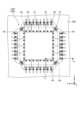
- FIG. 3 is an exemplary schematic plan view of the switch device according to the first embodiment.
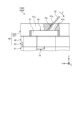
- FIG. 4 is an exemplary schematic side view (partial cross-sectional view) of a portion of the switch device of the first embodiment.
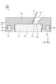
- FIG. 5 is a cross-sectional view taken along line VV of FIG.
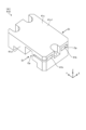
- FIG. 6 is an exemplary schematic perspective view of a cover member of the switch device according to the first embodiment.
- FIG. 7 is an exemplary schematic exploded perspective view of a portion of the switch device according to the first embodiment.
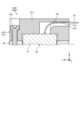
- FIG. 8 is an exemplary schematic cross-sectional view of a switch device according to a second embodiment, taken at a position equivalent to that of FIG.
- FIG. 9 is an exemplary schematic perspective view of a cover member of a switch device according to the third embodiment.
- FIG. 10 is an exemplary schematic cross-sectional view of a switch device according to a fourth embodiment, taken at the same position as in FIG. 5 .
- FIG. 11 is an exemplary schematic perspective view of a cover member of a switch device according to the fourth embodiment.
- FIG. 12 is an exemplary schematic cross-sectional view of a switch device according to a fifth embodiment, taken at a position equivalent to that of FIG. 5.
- FIG. 13 is an exemplary schematic perspective view of a cover member of a switch device according to the fifth embodiment.
- FIG. 14 is an exemplary schematic cross-sectional view of a switch device according to a sixth embodiment, taken at a position equivalent to that of FIG. 5.
- FIG. 15 is an exemplary schematic perspective view of a cover member of a switch device according to the sixth embodiment.
- FIG. 16 is an exemplary schematic plan view of the switch device according to the seventh embodiment.
- FIG. 17 is a cross-sectional view taken along line XVII-XVII of FIG.
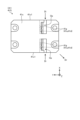
- FIG. 18 is an exemplary schematic plan view of a cover member of the switch device according to the seventh embodiment.
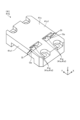
- FIG. 19 is an exemplary schematic perspective view of a cover member of a switch device according to the seventh embodiment.
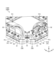
- FIG. 20 is an exemplary schematic perspective view of a switch device according to the eighth embodiment.
- FIG. 21 is an exemplary schematic perspective view of a switch device according to the ninth embodiment.
- ordinal numbers may be given for convenience to distinguish directions, parts, members, mechanisms, etc. Furthermore, ordinal numbers do not indicate priority or order, nor do they specify a number.
- the X direction is represented by an arrow X
- the Y direction is represented by an arrow Y
- the Z direction is represented by an arrow Z.
- the X direction, Y direction, and Z direction intersect with each other and are perpendicular to each other.
- Fig. 1 is a plan view of an optical communication device 1000 according to a first embodiment.
- the optical communication device 1000 includes a motherboard 200, an IC 300, and a plurality of switch devices 100.
- the optical communication device 1000 may also include a power supply module, a cooling fan, and the like (none of which are shown).
- Motherboard 200 has a plate-like shape that crosses the Z direction and spreads perpendicularly.
- Motherboard 200 has face 200a and face 200b.
- Face 200a faces the Z direction, crosses the Z direction, and is perpendicular to it.
- Face 200b faces the opposite direction to the Z direction on the opposite side to face 200a, crosses the Z direction, and is perpendicular to it.
- the multiple switch devices 100 are mounted on surface 200a, and the IC 300 is mounted on surface 200b. Note that the IC 300 may also be mounted on surface 200a.
- the IC300 controls the operation of the multiple switch devices 100 and transmits communication signals between the multiple switch devices 100.
- the IC300 is an example of a control circuit.
- the conductors (not shown) of the motherboard 200 and the conductors (not shown) of the switch device 100 are electrically connected via conductors (not shown) within the connector.
- the motherboard 200 is housed in a housing 1001.
- An optical connector array 1002 is provided on a part of the wall that constitutes the housing 1001.
- the optical fiber 32 (not shown in FIG. 1, see FIG. 2, etc.) is routed between the optical transceiver subassembly 30 mounted in each switch device 100 and an optical connector (not shown) provided in the optical connector array 1002.
- the direction in which the optical fiber 32 is pulled out from the switch device 100 may be different for each switch device 100, or may be the same for multiple switch devices 100.
- FIG. 2 is a perspective view of the switch device 100A (100) of the first embodiment.
- FIG. 3 is a plan view of the switch device 100A (100).
- FIG. 4 is a side view (partial cross-sectional view) of a portion of the switch device 100A (100) when viewed in the Y direction at the arrow IV in FIG. 2.
- FIG. 5 is a cross-sectional view taken along line V-V in FIG. 3.
- the switch device 100 is mounted on a motherboard 200. Note that in this embodiment, only one switch device 100 is mounted on the motherboard 200, but multiple switch devices 100 may be mounted on the motherboard 200.
- the motherboard 200 may also be referred to as an integrated board.
- the switch device 100 includes a substrate 10, a plurality of optical transceiver subassemblies 30, and a fixing mechanism 40 that fixes the optical transceiver subassemblies 30 to the substrate 10.
- the substrate 10 and the fixing mechanism 40 of the switch device 100 are referred to as a substrate assembly.
- the substrate assembly can be mounted on a motherboard 200.
- the substrate 10 also includes a switch ASIC 20 (see Figure 1), a heat dissipation mechanism for the optical transceiver subassemblies 30, a heat dissipation mechanism for the switch ASIC 20, and the like.
- the switch ASIC 20 is an example of a signal processing circuit.
- the substrate 10 can also be referred to as a daughter board.
- the substrate 10 has a square (rectangular) shape. Also, as shown in FIG. 5, the substrate 10 crosses the Z direction and spreads perpendicularly, has a plate shape, and has a surface 10a facing the Z direction and a surface 10b facing the opposite direction of the Z direction on the opposite side of the surface 10a. The surfaces 10a and 10b cross the Z direction and spread perpendicularly.
- the substrate 10 is, for example, a printed wiring board.
- the Z direction is an example of a first direction of the substrate 10, and can also be called the thickness direction of the substrate 10.
- the surface 10a is an example of a first surface
- the surface 10b is an example of a second surface. From the viewpoint of increasing the number of substrates 10 that can be mounted on the motherboard 200, the shorter the length of one side of the substrate 10, the better. For example, it is preferable that the length is 15 cm or less, and more preferably 10 cm or less.
- the optical transceiver subassemblies 30 shown in Figures 2 to 4 each receive an optical signal transmitted through an optical fiber 32 and output an electrical signal corresponding to the optical signal.
- the electrical signal output from the optical transceiver subassembly 30 is input to the switch ASIC via the socket 43 (see Figure 5) and conductors provided on the board 10.
- the optical transceiver subassembly 30 has a photodiode array (not shown) as a plurality of light receiving units that receive optical signals.
- each optical transceiver subassembly 30 receives an electrical signal from the switch ASIC via conductors provided on the board 10 and the socket 43, and outputs an optical signal corresponding to the electrical signal.
- the optical signal output from the optical transceiver subassembly 30 is coupled to the optical fiber 32 and transmitted through the optical fiber 32.
- the optical transceiver subassembly 30 has, for example, a VCSEL array (not shown, VCSEL: vertical cavity surface emitting laser) as a plurality of light emitting units that output optical signals.
- VCSEL array not shown, VCSEL: vertical cavity surface emitting laser
- the transmission capacity of each optical transceiver subassembly 30 should be large, for example, 400 Gb/s or more.
- the width of the optical transceiver subassembly 30 should be small, for example, preferably 10 mm or less, and more preferably 8 mm or less.
- the type of optical fiber 32 is not limited, and may be, for example, a single mode fiber, a multimode fiber, a ribbon fiber, a multicore fiber, etc.
- the optical transceiver subassemblies 30 are arranged along each side 10c of the substrate 10.
- the optical transceiver subassemblies 30 are mounted so as to cover the corresponding side 10c.
- each optical transceiver subassembly 30 is provided so as to straddle the side 10c, and has a portion located inside the side 10c and a portion located outside the side 10c. This has the advantage that it is easier to avoid interference between the optical fiber 32 extending from the optical transceiver subassembly 30 and other components such as a switch ASIC mounted on the substrate 10, and the substrate 10 can be made smaller.
- the optical transceiver subassemblies 30 are fixed to the substrate 10 by a fixing mechanism 40 provided on each side 10c of the substrate 10.
- a fixing mechanism 40 is provided on each of the four sides 10c, i.e., a total of four fixing mechanisms 40, and are shared by the optical transceiver subassemblies 30 (eight in this embodiment, as an example) arranged along each side 10c.
- the fixing mechanism 40 is shared by the optical transceiver subassemblies 30, which has the advantage that the mounting structure of the fixing mechanism 40 to the substrate 10 can be simplified and the number of parts can be reduced compared to when the optical transceiver subassemblies 30 are fixed to the substrate 10 by their own fixing mechanisms, thereby reducing the effort and cost required to manufacture the switch device 100.
- a total of 32 optical transceiver subassemblies 30 can be mounted on the four sides. For example, if the transmission capacity of each optical transceiver subassembly 30 is 400 Gb/s or more, the transmission capacity of the switch device 100 will be 12.8 Tb/s or more.
- the switch ASIC is mounted, for example, by flip chip mounting, on the substrate 10 at a position away from each of the sides 10c of the substrate 10 (approximately the center of the substrate 10 in this embodiment).
- the switch ASIC controls the operation of each optical transceiver subassembly 30.
- the switch ASIC is an example of a semiconductor integrated circuit.
- the fixing mechanism 40 has an upper member 41, an intermediate member 42, and a socket 43. These components of the fixing mechanism 40 are integrated by a fastener 46 such as a screw. Among the components of the fixing mechanism 40, the intermediate member 42 and the socket 43 are shared by all the optical transceiver subassemblies 30 included in the group of multiple optical transceiver subassemblies 30 along the side 10c of the substrate 10. As shown in Figure 5, the fixing mechanism 40 fixes the optical transceiver subassembly 30 located near the side 10c of the substrate 10 to the substrate 10 in a state in which it is sandwiched in the thickness direction of the substrate 10.
- the fixing mechanism 40 includes components fixed to the board 10 and components detachable from the board 10.
- the intermediate member 42 and the socket 43 are fixed to the board 10, and the upper member 41 is configured to be detachable from the intermediate member 42, i.e., the board 10.
- the upper member 41 is attached to the intermediate member 42 by a fastener 46 configured as a removable screw.
- the optical transceiver subassembly 30 can be removed by moving it in the Z direction, and can be attached by moving it in the opposite direction to the Z direction.
- the optical transceiver subassembly 30 is detachably fixed to the board 10 via the fixing mechanism 40 configured in this way.
- the upper member 41 is not shared by all of the multiple optical transceiver subassemblies 30 along side 10c, but is shared only by two adjacent optical transceiver subassemblies 30 along side 10c.
- This has the advantage that, for example, it is possible to simultaneously facilitate removal of individual optical transceiver subassemblies 30 while sharing parts, and that the positioning accuracy can be improved by reducing the effects of bending of the fixing mechanism 40 and manufacturing variations in the components of the fixing mechanism 40 and the optical transceiver subassemblies 30.
- this configuration is just one example, and the upper member 41 may be shared by all of the multiple optical transceiver subassemblies 30 along side 10c.
- the optical transceiver subassembly 30 has an optical transceiver housing 31 and multiple optical fibers 32 (see FIG. 2).
- the optical transceiver subassembly 30 will be described as being fixed to the board 10.
- the housing 31 contains the board, the light receiving unit, the light emitting unit, and other components described above.
- the housing 31 has a surface 31a facing in the opposite direction to the Z direction.
- Surface 31a is provided with an electrical interface 31a1 having an array of electrodes (not shown) and a heat dissipation surface 31a2.
- the electrical interface 31a1 and the heat dissipation surface 31a2 both face in the opposite direction to the Z direction and are aligned substantially along surface 10a of the board 10 and in a direction intersecting side 10c of the board 10 (the X direction in the optical transceiver subassembly 30 shown in FIG. 5).
- a heat generating element inside the optical transceiver subassembly 30 is aligned in the Z direction with the heat dissipation surface 31a2.
- the heat dissipation surface 31a2 may also be referred to as a heat dissipation section, and the electrical interface 31a1 may also be referred to as a first electrical interface.
- the optical fibers 32 extend from a portion of the housing 31 away from the surface 31a, specifically, from a portion on the opposite side of the heat dissipation surface 31a2 that is aligned with the heat dissipation surface 31a2 in the Z direction.
- the socket 43, intermediate member 42, and upper member 41 are placed on the substrate 10 in this order.
- the wall 41c of the upper member 41 that intersects with the Z direction is positioned offset in the Z direction with respect to the housing 31 of the optical transceiver subassembly 30, covers the housing 31 from the side opposite the board 10, and presses the housing 31 in the opposite direction of the Z direction toward the board 10 and the socket 43.
- the upper member 41 is an example of a cover member.
- the upper member 41 has an opening Op that penetrates the upper member 41 in the Z direction.
- the optical fiber 32 passes through the opening Op and extends outside the upper member 41.
- the intermediate member 42 has an opening 42a as a through hole extending in the Z direction.
- the side of the opening 42a has the function of roughly guiding the housing 31 of the optical transceiver subassembly 30 in the X and Y directions when it is attached.
- the upper member 41 can also be referred to as a guide member.
- the socket 43 is placed on the surface 10a of the substrate 10 and supports the housing 31 of the optical transceiver subassembly 30.
- the socket 43 is provided with an electrical interface 43a and an opening 43b.
- the electrical interface 43a may also be referred to as a second electrical interface.
- the electrical interface 43a faces and contacts the electrical interface 31a1 provided on the housing 31 of the optical transceiver subassembly 30, and has a conductor 43a1 electrically connected to each of the multiple electrodes provided on the electrical interface 31a1.
- the conductor 43a1 can be configured, for example, as a contact terminal having an elastically expandable pin extending in the Z direction.
- the conductor 43a1 is electrically connected to a conductor (not shown) of the board 10. Also, as described above, a load is applied to the optical transceiver subassembly 30 in the opposite direction to the Z direction by the upper member 41, thereby realizing a stable electrical connection between the electrical interface 31a1 and the conductor 43a1.
- Each electrode of the electrical interface 31a1 of the optical transceiver subassembly 30 is electrically connected to the conductor of the switch ASIC via the conductor 43a1 of the electrical interface 43a of the socket 43 and the conductor of the board 10.
- Providing a socket 43 with an electrical interface 43a has the advantage that it is easier to construct a configuration that ensures the required positioning accuracy of multiple electrodes compared to, for example, providing the electrical interface 43a directly on the substrate 10.
- the thermal conductivity of the insulator 43a2 that is positioned around the conductor 43a1 and supports the conductor 43a1 is lower than the thermal conductivity of the heat dissipation surface 31a2.
- the opening 43b exposes the heat dissipation surface 31a2 provided on the housing 31 of the optical transceiver subassembly 30 in the opposite direction to the Z direction.
- the opening 43b is provided, for example, as a through hole or a notch that penetrates the socket 43 in the Z direction.
- the portion 51a of the member 51 passes through the opening 43b, is adjacent to the heat dissipation surface 31a2 via the flexible heat-conducting sheet 47, and is thermally connected to the heat dissipation surface 31a2.
- the member 51 is made of a material with a relatively high thermal conductivity, and functions as a heat dissipation member that dissipates heat generated within the housing 31 of the optical transceiver subassembly 30 via the heat dissipation surface 31a2 and the portion 51a.
- optical fiber guide mechanism 4 the optical fiber 32 passes through an opening Op provided in the upper member 41A (41).
- the upper member 41 has a surface 41a and a surface 41b as side surfaces that form the opening Op.
- the surface 41a is configured so that the optical fiber 32 comes into contact with the surface 41a when the optical transceiver subassembly 30 and the upper member 41 are fixed to the substrate 10, in other words, when the switch device 100 is assembled, and the optical fiber 32 that comes into contact with the surface 41a is guided along the surface 41a.
- the surface 41a is configured as an inclined surface that is inclined in the opposite direction to the Y direction as it approaches the Z direction. Therefore, as shown in FIG. 4, the optical fiber 32 is guided by the surface 41a, bends approximately along the surface 41a, and extends in a direction inclined with respect to the Z direction. In other words, the surface 41a guides the optical fiber 32 to be in a curved state.
- the surface 41a has specifications such as its position, shape, and inclination angle set so that the optical fiber 32 bends with a radius of curvature larger than the minimum bending radius. This configuration prevents the optical fiber 32 bent along the surface 41a from experiencing excessive bending loss or from breaking.
- the opening Op forms a guide portion, and the surface 41a is an example of the guide portion and the first surface.
- the upper member 41 may be made of a material with high heat dissipation properties, such as aluminum or a copper-tungsten alloy.
- surface 41b faces surface 41a and is spaced apart from surface 41b.
- Surface 41a is an example of a second surface.
- the specifications of the surface 41b such as its position, shape, and inclination angle, are set so that when the bent optical fiber 32 comes into contact with the surface 41b, the optical fiber 32 is bent at a radius of curvature larger than the minimum bending radius, in other words, so that the optical fiber 32 does not bend at a radius smaller than the minimum bending radius by coming into contact with the surface 41b. With this configuration, the optical fiber 32 is prevented from breaking.
- FIG. 6 is a perspective view of the upper member 41A (41).
- the opening Op penetrates the wall 41c of the upper member 41 in the Z direction.
- the opening Op is provided as a notch that opens in the side surface 41c1 of the wall 41c.
- the optical fiber 32 can be inserted by moving it in the direction Di through the open portion of the notch. If the opening Op were configured as a through hole, there is a risk that the work sequence will be restricted or the work will be more time-consuming, such as the end of the optical fiber 32 having to be passed through the opening Op when the optical fiber 32 is not connected to the housing 31 or the connector array.
- the opening Op is provided as a notch, and the optical fiber 32 can be inserted into the opening Op in a direction intersecting the extension direction.
- This has the effect of, for example, improving the workability of the optical fiber 32 arrangement, and making it easier to reduce the effort and time required for manufacturing and maintenance.
- a stopper 41d is provided to prevent the optical fiber 32, which penetrates the opening Op and contacts the surface 41a, from moving along the surface 41a in a direction intersecting the extension direction of the optical fiber 32, in this case, the X direction or the direction opposite to the X direction. This has the effect of preventing, for example, the optical fiber 32 from bending more significantly or coming out of the opening Op configured as a notch.
- FIG. 7 is an exploded perspective view showing a state before assembling the upper member 41 as a cover member in the switch device 100 or a state after removal.
- the upper member 41 is integrated with the intermediate member 42 by connecting the fastener 46 passing through the through hole 41e of the upper member 41 to the female screw hole 42b of the intermediate member 42.
- the upper member 41 can be removed from the intermediate member 42 by removing the fastener 46 from the assembled state.
- the optical fiber 32 can be inserted into the opening Op from the open portion of the notch.
- the upper member 41 is moved in the opposite direction of the Z direction toward a predetermined mounting position with the optical fiber 32 inserted in the opening Op, so that the optical fiber 32 comes into contact with the surface 41a and is bent as shown in FIG. 4.
- the upper member 41 (cover member) can be used to appropriately set the routing direction of the optical fiber 32 at the portion where the optical fiber 32 exits from the upper member 41.
- FIG. 8 is a cross-sectional view of a portion of the switch device 100B (100) according to the second embodiment where the optical transceiver subassembly 30 is provided, taken at the same position as in FIG.
- the inclination of the surface 41a on the upper member 41B (41) in the Z direction is different from the inclination of the surface 41a in the Z direction in the first embodiment (see FIG. 4). Accordingly, the arrangement direction of the optical fiber 32 at the position where it exits the upper member 41 is different between this embodiment and the first embodiment. In this way, by changing the specifications of the surface 41a, the arrangement direction of the optical fiber 32 at the position where the optical fiber 32 exits the upper member 41 can be appropriately set.
- the mechanism for fixing the upper member 41B (41) to the intermediate member 42 differs from that in the first embodiment.
- the magnet 70c provided on the intermediate member 42 and the magnet 70d provided on the upper member 41 face each other, forming an attraction mechanism using magnetic force.
- the magnetic force is set to a magnitude that allows the upper member 41 to be detached from the intermediate member 42 by a force applied by an operator or a robot.
- a magnet may be used in the mechanism for fixing the optical transceiver subassembly 30 to the substrate 10.
- a magnet provided in the socket 43 (see FIG. 5) and a magnet provided in the optical transceiver subassembly 30 may face each other to form an adhesion mechanism using magnetic force.
- the magnetic force is set to a level that allows the optical transceiver subassembly 30 to be removed from the socket 43 by the force applied by an operator or robot.
- the magnet may be provided in a location other than the socket 43.
- FIG. 9 is a perspective view of the upper member 41C (41) of the third embodiment.
- a surface 41a is formed on a protruding portion 41f protruding from a side surface 41c1, and the opening Op has a substantially U-shape when viewed in the opposite direction to the Z direction. This provides an effect that, for example, the shape of the opening Op becomes more complicated, making it difficult for the optical fiber 32 to come off the opening Op.
- Fig. 10 is a cross-sectional view of a portion of the switch device 100D (100) according to the fourth embodiment where the optical transceiver subassembly 30 is provided, taken at the same position as in Fig. 5.
- Fig. 11 is a perspective view of the upper member 41D (41).
- optical fiber 32 extends in the opposite direction to the Y direction at the position where it exits from upper member 41D.
- optical fiber 32 can be bent with a radius of curvature larger than the minimum bending radius.
- surface 41b faces surface 41a and is spaced apart from surface 41a.
- Surface 41b faces the Z direction and intersects with and is perpendicular to the Z direction. In this case, too, by appropriately setting the specifications of surface 41b, such as by appropriately setting the distance of surface 41b from surface 41a, it is possible to prevent optical fiber 32 from bending at a radius of curvature smaller than the minimum bending radius.
- Fig. 12 is a cross-sectional view of a portion of the switch device 100E (100) according to the fifth embodiment where the optical transceiver subassembly 30 is provided, taken at the same position as in Fig. 5,
- Fig. 13 is a perspective view of an upper member 41E (41) according to the fifth embodiment
- Fig. 14 is a cross-sectional view of a portion of the switch device 100F (100) according to the sixth embodiment where the optical transceiver subassembly 30 is provided, taken at the same position as in Fig. 5, and
- Fig. 15 is a perspective view of an upper member 41F (41) according to the sixth embodiment.
- a connector 33 for an optical fiber 32 is attached to the housing 31 of the optical transceiver subassembly 30.
- the connector 33 of the fifth embodiment pulls out the optical fiber 32 in the Z direction
- the connector 33 of the sixth embodiment pulls out the optical fiber 32 in the opposite direction to the Y direction.
- the direction of the optical fiber 32 at the portion exiting the upper member 41 can be appropriately set by appropriately setting the shape and structure of the upper members 41E, 41F (41) and appropriately setting the specifications of the surface 41a.
- FIG. 16 is a plan view of a switch device 100G (100) according to the sixth embodiment.
- the optical fibers 32 in the optical transceiver subassemblies 30 provided along the same side 10c of the substrate 10 are drawn out in the same direction.
- the drawing out direction may also be referred to as the guide direction of the guide portion.
- the pull-out direction of the optical fiber 32 is different for each side 10c. That is, the pull-out direction of the optical fiber 32 in the multiple optical transceiver subassemblies 30 arranged along sides 10c1 and 10c3 is a direction between the Z direction and the opposite direction of the X direction, the pull-out direction of the optical fiber 32 in the multiple optical transceiver subassemblies 30 arranged along side 10c2 is a direction between the Z direction, the opposite direction of the X direction, and the opposite direction of the Y direction, and the pull-out direction of the optical fiber 32 in the multiple optical transceiver subassemblies 30 arranged along side 10c4 is a direction between the Z direction, the opposite direction of the X direction, and the Y direction.
- This pull-out direction can be set by the upper member 41.
- multiple upper members 41 having the same shape are lined up along each side 10c. This makes it possible to make the pull-out direction of the optical fibers 32 the same in multiple optical transceiver subassemblies 30 arranged along the same side 10c of the substrate 10.
- the shape of the upper members 41 is different for each side 10c. That is, the shapes of the upper members 41 aligned along side 10c1, the upper members 41 aligned along side 10c2, the upper members 41 aligned along side 10c3, and the upper members aligned along side 10c4 are different from one another.
- the setting of the pull-out direction of the optical fiber 32 i.e., the wiring direction, is not limited to the example in FIG. 16, and the optical fiber 32 may be pulled out in a direction different from that in FIG. 16, or upper members 41 of different shapes may be provided along the same side 10c, and optical transceiver subassemblies 30 with different pull-out directions of the optical fiber 32 may be provided along the same side 10c.
- FIG. 17 is a cross-sectional view taken along line XVII-XVII in FIG. 16.
- FIG. 18 is a plan view of the upper member 41G included in the cross-sectional view of FIG. 17, and
- FIG. 19 is a perspective view of the upper member 41G.
- the upper members 41G are aligned along the edge 10c2 of the substrate 10.
- the upper member 41G shown in Figures 17 to 19 has a groove 41g in the opening Op that guides the optical fiber 32.
- the groove 41g extends in the opposite direction to the Y direction as it approaches the Z direction, and as shown in Figure 18, it extends in the opposite direction to the X direction as it approaches the opposite direction to the Y direction. Therefore, the routing direction Dr of the optical fiber 32 accommodated in the groove 41g is a direction between the Z direction, the opposite direction of the X direction, and the opposite direction of the Y direction.
- the groove 41g contacts and guides the optical fiber 32, and prevents the optical fiber 32 from moving in a direction intersecting the direction in which the optical fiber 32 extends from the groove 41g.
- the groove 41g functions as the surface 41a and the stopper 41d.
- the wiring direction of the optical fiber 32 can be set arbitrarily.
- the pull-out direction (wiring direction) of the optical fiber 32 of the multiple optical transceiver subassemblies 30 can be set in various ways.
- Fig. 20 is a perspective view of a part of the switch device 100H (100) of the eighth embodiment.
- the upper member 41H (41) has a protruding portion 41h protruding from the wall 41c.
- the protruding portion 41h holds the optical fiber 32 at a plurality of points at a predetermined interval, thereby guiding the optical fiber 32 in a predetermined direction in a bent state.
- the upper member 41I (41) has a protruding portion 41i protruding from the wall 41c.
- the protruding portion 41i holds the optical fiber 32 within a predetermined range, thereby guiding the optical fiber 32 in a predetermined direction in a bent state.
- these upper members 41H, 41I (41) have an effect of improving the protection of the optical fiber 32.
- FIG. 21 is a perspective view of the switch device 100J (100) of the ninth embodiment.
- the upper member 41J (41) covers the housings 31 of the optical transceiver subassemblies 30. That is, in this embodiment, it can be said that the upper members 41 in each of the above embodiments are integrated. According to this configuration, the number of parts of the switch device 100J can be reduced, and therefore, the effect of reducing the effort and time required for manufacturing the switch device 100J can be obtained.
- the upper member 41J covers the housings 31 of all the optical transceiver subassemblies 30 arranged along the same side 10c of the substrate 10, but is not limited thereto.
- the upper member 41 may cover the housings 31 of multiple optical transceiver subassemblies 30 that are a portion of all optical transceiver subassemblies 30 along the same side 10c of the substrate 10, or may cover the housings 31 of multiple optical transceiver subassemblies 30 along adjacent sides 10c via a corner of the substrate 10, or may cover the housings 31 of all optical transceiver subassemblies 30 provided in the switch device 100.
- the present invention can be used in substrate assemblies and optical communication devices.
Landscapes
- Physics & Mathematics (AREA)
- General Physics & Mathematics (AREA)
- Optics & Photonics (AREA)
- Optical Couplings Of Light Guides (AREA)
Priority Applications (1)
| Application Number | Priority Date | Filing Date | Title |
|---|---|---|---|
| JP2025510590A JPWO2024203634A1 (https=) | 2023-03-31 | 2024-03-19 |
Applications Claiming Priority (2)
| Application Number | Priority Date | Filing Date | Title |
|---|---|---|---|
| JP2023058764 | 2023-03-31 | ||
| JP2023-058764 | 2023-03-31 |
Publications (1)
| Publication Number | Publication Date |
|---|---|
| WO2024203634A1 true WO2024203634A1 (ja) | 2024-10-03 |
Family
ID=92904841
Family Applications (1)
| Application Number | Title | Priority Date | Filing Date |
|---|---|---|---|
| PCT/JP2024/010793 Ceased WO2024203634A1 (ja) | 2023-03-31 | 2024-03-19 | 基板アセンブリおよび光通信装置 |
Country Status (2)
| Country | Link |
|---|---|
| JP (1) | JPWO2024203634A1 (https=) |
| WO (1) | WO2024203634A1 (https=) |
Citations (9)
| Publication number | Priority date | Publication date | Assignee | Title |
|---|---|---|---|---|
| WO2009128413A1 (ja) * | 2008-04-14 | 2009-10-22 | 古河電気工業株式会社 | 光モジュール取付ユニット及び光モジュール |
| JP2011253180A (ja) * | 2010-05-03 | 2011-12-15 | Avago Technologies Fiber Ip (Singapore) Pte Ltd | 並列光トランシーバ・モジュールと共に使用する、浮遊物体からこのモジュールの部品を保護するための保護ソケット |
| JP2013104884A (ja) * | 2011-11-10 | 2013-05-30 | Yazaki Corp | 光路変換部材及び光モジュール |
| US20140203175A1 (en) * | 2011-12-30 | 2014-07-24 | Mauro J. Kobrinsky | Optical i/o system using planar light-wave integrated circuit |
| JP2015031801A (ja) * | 2013-08-01 | 2015-02-16 | 富士通株式会社 | 光モジュールおよび光ファイバの実装方法 |
| WO2017138152A1 (ja) * | 2016-02-12 | 2017-08-17 | 住友電気工業株式会社 | 光トランシーバの放熱装置及び光通信装置 |
| JP2020008626A (ja) * | 2018-07-04 | 2020-01-16 | 古河電気工業株式会社 | 光路曲げコネクタ、光路曲げコネクタアッセンブリ |
| US20200278508A1 (en) * | 2019-02-28 | 2020-09-03 | Teramount Ltd. | Fiberless co-packaged optics |
| JP2023150085A (ja) * | 2022-03-31 | 2023-10-16 | 古河電気工業株式会社 | 基板アセンブリ |
-
2024
- 2024-03-19 JP JP2025510590A patent/JPWO2024203634A1/ja active Pending
- 2024-03-19 WO PCT/JP2024/010793 patent/WO2024203634A1/ja not_active Ceased
Patent Citations (9)
| Publication number | Priority date | Publication date | Assignee | Title |
|---|---|---|---|---|
| WO2009128413A1 (ja) * | 2008-04-14 | 2009-10-22 | 古河電気工業株式会社 | 光モジュール取付ユニット及び光モジュール |
| JP2011253180A (ja) * | 2010-05-03 | 2011-12-15 | Avago Technologies Fiber Ip (Singapore) Pte Ltd | 並列光トランシーバ・モジュールと共に使用する、浮遊物体からこのモジュールの部品を保護するための保護ソケット |
| JP2013104884A (ja) * | 2011-11-10 | 2013-05-30 | Yazaki Corp | 光路変換部材及び光モジュール |
| US20140203175A1 (en) * | 2011-12-30 | 2014-07-24 | Mauro J. Kobrinsky | Optical i/o system using planar light-wave integrated circuit |
| JP2015031801A (ja) * | 2013-08-01 | 2015-02-16 | 富士通株式会社 | 光モジュールおよび光ファイバの実装方法 |
| WO2017138152A1 (ja) * | 2016-02-12 | 2017-08-17 | 住友電気工業株式会社 | 光トランシーバの放熱装置及び光通信装置 |
| JP2020008626A (ja) * | 2018-07-04 | 2020-01-16 | 古河電気工業株式会社 | 光路曲げコネクタ、光路曲げコネクタアッセンブリ |
| US20200278508A1 (en) * | 2019-02-28 | 2020-09-03 | Teramount Ltd. | Fiberless co-packaged optics |
| JP2023150085A (ja) * | 2022-03-31 | 2023-10-16 | 古河電気工業株式会社 | 基板アセンブリ |
Also Published As
| Publication number | Publication date |
|---|---|
| JPWO2024203634A1 (https=) | 2024-10-03 |
Similar Documents
| Publication | Publication Date | Title |
|---|---|---|
| TWI452371B (zh) | 中平面安置之光學通信系統及提供平行光學通信模組之高密度中平面安置之方法 | |
| JP5224416B2 (ja) | 光モジュール取付ユニット及び光モジュール | |
| CN101995621B (zh) | 光电转换模块 | |
| JP6464653B2 (ja) | 光モジュール及び光トランシーバ | |
| JP4238187B2 (ja) | 光電気複合型コネクタ及びそれを用いた基板 | |
| US7766558B2 (en) | Optical transceiver | |
| US20120182688A1 (en) | Direct cooling system and method for transceivers | |
| JP2012009851A (ja) | アクティブ光ケーブルで使用するための民生用入力/出力(cio)光トランシーバ・モジュール及び方法 | |
| US8920048B2 (en) | Communications module with a shell assembly having thermal mechanical features | |
| WO2017195714A1 (ja) | トランシーバモジュール、トランシーバモジュール用リセプタクルアセンブリ、および、トランシーバモジュールアセンブリ | |
| JP2018146639A (ja) | 光トランシーバ | |
| CN115701854A (zh) | 用于光学通信系统的光学插座连接器 | |
| JP2025105950A (ja) | 光装置、発光装置、光ケーブル、及び光装置の接続方法 | |
| US11199671B2 (en) | Glass-as-a-platform (GaaP)-based photonic assemblies comprising shaped glass plates | |
| CN101726809B (zh) | 光学收发器 | |
| US8172467B2 (en) | Optical backplane connector, photoelectric conversion module and optical backplane | |
| US20060126306A1 (en) | Multi-power optoelectric packages | |
| WO2024203634A1 (ja) | 基板アセンブリおよび光通信装置 | |
| JP2010062087A (ja) | 光電気モジュール | |
| CN116047676B (zh) | 光发射组件和光模块 | |
| JP5075139B2 (ja) | 並列光伝送装置 | |
| US20250284076A1 (en) | Optical module with thermal management for cpo configuration and optical communication system thereof | |
| US20250189735A1 (en) | Optical device and optical transceiver | |
| US20250035868A1 (en) | Optical module | |
| CN214895918U (zh) | 光学收发模块及光纤缆线模块 |
Legal Events
| Date | Code | Title | Description |
|---|---|---|---|
| 121 | Ep: the epo has been informed by wipo that ep was designated in this application |
Ref document number: 24779759 Country of ref document: EP Kind code of ref document: A1 |
|
| ENP | Entry into the national phase |
Ref document number: 2025510590 Country of ref document: JP Kind code of ref document: A |
|
| WWE | Wipo information: entry into national phase |
Ref document number: 2025510590 Country of ref document: JP |
|
| NENP | Non-entry into the national phase |
Ref country code: DE |
|
| 122 | Ep: pct application non-entry in european phase |
Ref document number: 24779759 Country of ref document: EP Kind code of ref document: A1 |