WO2024203295A1 - 光学フィルムの製造方法 - Google Patents
光学フィルムの製造方法 Download PDFInfo
- Publication number
- WO2024203295A1 WO2024203295A1 PCT/JP2024/009614 JP2024009614W WO2024203295A1 WO 2024203295 A1 WO2024203295 A1 WO 2024203295A1 JP 2024009614 W JP2024009614 W JP 2024009614W WO 2024203295 A1 WO2024203295 A1 WO 2024203295A1
- Authority
- WO
- WIPO (PCT)
- Prior art keywords
- optical film
- film
- thickness
- layer
- liquid crystal
- Prior art date
- Legal status (The legal status is an assumption and is not a legal conclusion. Google has not performed a legal analysis and makes no representation as to the accuracy of the status listed.)
- Ceased
Links
Images
Classifications
-
- B—PERFORMING OPERATIONS; TRANSPORTING
- B29—WORKING OF PLASTICS; WORKING OF SUBSTANCES IN A PLASTIC STATE IN GENERAL
- B29D—PRODUCING PARTICULAR ARTICLES FROM PLASTICS OR FROM SUBSTANCES IN A PLASTIC STATE
- B29D11/00—Producing optical elements, e.g. lenses or prisms
- B29D11/0074—Production of other optical elements not provided for in B29D11/00009- B29D11/0073
- B29D11/00788—Producing optical films
-
- B—PERFORMING OPERATIONS; TRANSPORTING
- B08—CLEANING
- B08B—CLEANING IN GENERAL; PREVENTION OF FOULING IN GENERAL
- B08B7/00—Cleaning by methods not provided for in a single other subclass or a single group in this subclass
- B08B7/0028—Cleaning by methods not provided for in a single other subclass or a single group in this subclass by adhesive surfaces
-
- B—PERFORMING OPERATIONS; TRANSPORTING
- B29—WORKING OF PLASTICS; WORKING OF SUBSTANCES IN A PLASTIC STATE IN GENERAL
- B29C—SHAPING OR JOINING OF PLASTICS; SHAPING OF MATERIAL IN A PLASTIC STATE, NOT OTHERWISE PROVIDED FOR; AFTER-TREATMENT OF THE SHAPED PRODUCTS, e.g. REPAIRING
- B29C59/00—Surface shaping of articles, e.g. embossing; Apparatus therefor
- B29C59/02—Surface shaping of articles, e.g. embossing; Apparatus therefor by mechanical means, e.g. pressing
-
- B—PERFORMING OPERATIONS; TRANSPORTING
- B29—WORKING OF PLASTICS; WORKING OF SUBSTANCES IN A PLASTIC STATE IN GENERAL
- B29D—PRODUCING PARTICULAR ARTICLES FROM PLASTICS OR FROM SUBSTANCES IN A PLASTIC STATE
- B29D11/00—Producing optical elements, e.g. lenses or prisms
- B29D11/00634—Production of filters
- B29D11/00644—Production of filters polarizing
-
- B—PERFORMING OPERATIONS; TRANSPORTING
- B29—WORKING OF PLASTICS; WORKING OF SUBSTANCES IN A PLASTIC STATE IN GENERAL
- B29D—PRODUCING PARTICULAR ARTICLES FROM PLASTICS OR FROM SUBSTANCES IN A PLASTIC STATE
- B29D11/00—Producing optical elements, e.g. lenses or prisms
- B29D11/0073—Optical laminates
-
- C—CHEMISTRY; METALLURGY
- C09—DYES; PAINTS; POLISHES; NATURAL RESINS; ADHESIVES; COMPOSITIONS NOT OTHERWISE PROVIDED FOR; APPLICATIONS OF MATERIALS NOT OTHERWISE PROVIDED FOR
- C09J—ADHESIVES; NON-MECHANICAL ASPECTS OF ADHESIVE PROCESSES IN GENERAL; ADHESIVE PROCESSES NOT PROVIDED FOR ELSEWHERE; USE OF MATERIALS AS ADHESIVES
- C09J7/00—Adhesives in the form of films or foils
-
- G—PHYSICS
- G02—OPTICS
- G02B—OPTICAL ELEMENTS, SYSTEMS OR APPARATUS
- G02B5/00—Optical elements other than lenses
- G02B5/30—Polarising elements
-
- B—PERFORMING OPERATIONS; TRANSPORTING
- B29—WORKING OF PLASTICS; WORKING OF SUBSTANCES IN A PLASTIC STATE IN GENERAL
- B29C—SHAPING OR JOINING OF PLASTICS; SHAPING OF MATERIAL IN A PLASTIC STATE, NOT OTHERWISE PROVIDED FOR; AFTER-TREATMENT OF THE SHAPED PRODUCTS, e.g. REPAIRING
- B29C59/00—Surface shaping of articles, e.g. embossing; Apparatus therefor
- B29C59/02—Surface shaping of articles, e.g. embossing; Apparatus therefor by mechanical means, e.g. pressing
- B29C2059/027—Grinding; Polishing
-
- B—PERFORMING OPERATIONS; TRANSPORTING
- B29—WORKING OF PLASTICS; WORKING OF SUBSTANCES IN A PLASTIC STATE IN GENERAL
- B29C—SHAPING OR JOINING OF PLASTICS; SHAPING OF MATERIAL IN A PLASTIC STATE, NOT OTHERWISE PROVIDED FOR; AFTER-TREATMENT OF THE SHAPED PRODUCTS, e.g. REPAIRING
- B29C2793/00—Shaping techniques involving a cutting or machining operation
- B29C2793/0009—Cutting out
Definitions
- the present invention relates to a method for producing an optical film.
- Image display devices such as liquid crystal display devices and electroluminescence (EL) display devices (e.g., organic EL display devices), are rapidly becoming popular.
- EL electroluminescence
- image display devices optical components such as polarizing components and phase difference components are generally used to realize image display and improve image display performance (see, for example, Patent Document 1).
- Re(550) is the in-plane retardation measured with light having a wavelength of 550 nm at 23° C.
- Retardation in the thickness direction (Rth) is the retardation in the thickness direction measured with light having a wavelength of ⁇ nm at 23° C.
- Rth(550) is the retardation in the thickness direction measured with light having a wavelength of 550 nm at 23° C.
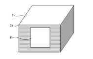
- FIG. 1 is a perspective view showing an optical film according to one embodiment of the present invention, showing a state in which multiple optical films are stacked.
- Optical film 2 can be obtained, typically, by cutting the outer peripheral surface of the optical film body so as to obtain a desired shape in plan view.
- End surface 2a of optical film 2 is a machined surface that has been subjected to cutting.
- Cutting can be performed simultaneously on multiple optical film bodies, for example, from the viewpoint of manufacturing efficiency.
- cutting can be performed on multiple optical film bodies in a stacked state by stacking multiple optical film bodies to form an assembly (also called a workpiece). Note that FIG. 1 shows the state after cutting has been performed on the workpiece.
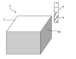
- FIG. 2 is a schematic perspective view for explaining an example of cutting process.
- a plurality of optical film bodies 3 are stacked to form a workpiece 4.
- each optical film body 3 is cut in advance into any appropriate shape depending on the purpose. In the example shown in FIG. 2, the optical film body 3 is cut into a rectangle, but it may be cut into other shapes (e.g., a circle).
- the number of optical film bodies 3 forming the workpiece 4 is not particularly limited, but may be, for example, 10 to 200 sheets, or may be 10 to 100 sheets.
- the thickness of the workpiece 4 is, for example, 5 mm to 50 mm.
- the outer peripheral surface 4a of the workpiece 4 is cut by the cutting part 6 of the cutting tool. Specifically, the cutting blade 8 provided on the cutting part 6 is brought into contact with the outer peripheral surface 4a of the workpiece 4 to cut the outer peripheral surface 4a of the workpiece 4.
- the cutting part 6 of the end mill which is a cutting tool, is rotated on its axis while the end mill is moved along the outer peripheral surface 4a of the workpiece 4 to perform cutting.
- the rotation speed of the cutting part 6 is, for example, 1000 rpm to 60000 rpm.
- the feed speed of the cutting part 6 is, for example, 500 mm/min to 10000 mm/min.
- the cutting process may be performed over the entire outer peripheral surface 4a of the workpiece 4, or may be selectively performed at a specified portion. During cutting, the workpiece 4 may be fixed by a fixture (not shown).
- the end surface 2a which is the processed surface of the optical film 2 is preferably free of fuzz produced by the cutting process.
- fuzz include poor cutting or remaining cut areas.
- the fuzz may be whisker-like protrusions, some of which are connected to the end surface of the optical film.
- the fuzz may contain components derived from the materials contained in the optical film.
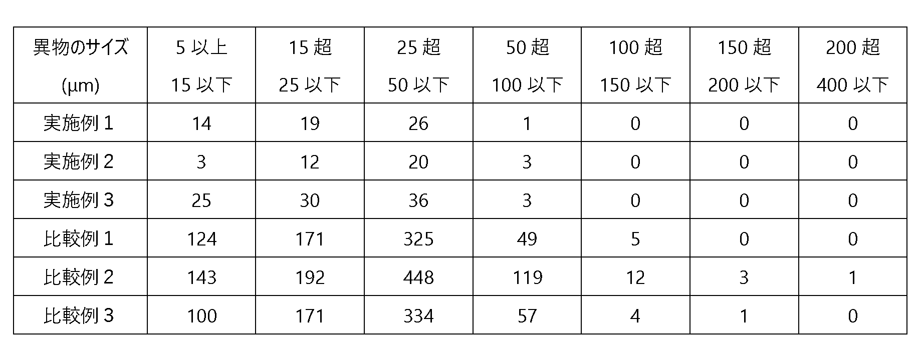
- the amount of foreign matter having a major axis exceeding 150 ⁇ m per unit length of 10 mm in a direction perpendicular to the thickness direction of the end face 2a of the optical film 2 is preferably 3 or less, more preferably 2 or less, even more preferably 1 or less, and particularly preferably 0.
- the amount of foreign matter having a major axis exceeding 50 ⁇ m and not more than 150 ⁇ m per unit length of 10 mm in a direction perpendicular to the thickness direction of the end face 2a of the optical film 2 is preferably 10 or less, more preferably 5 or less, even more preferably 3 or less, and particularly preferably 1 or less.
- the amount of foreign matter having a major axis exceeding 100 ⁇ m and not more than 150 ⁇ m per unit length of 10 mm in a direction perpendicular to the thickness direction of the end face 2a of the optical film 2 is preferably 3 or less, more preferably 2 or less, even more preferably 1 or less, and particularly preferably 0 or less.
- the number of foreign particles with a major axis exceeding 50 ⁇ m and not exceeding 100 ⁇ m per unit length of 10 mm in the direction perpendicular to the thickness direction of the end face 2a of the optical film 2 is preferably 10 or less, more preferably 5 or less, even more preferably 3 or less, and particularly preferably 1 or less.
- the major axis refers to the maximum straight-line distance between any two points on the cross-sectional diagram.
- the optical film can be typically applied to image display devices.
- image display devices foreign matter arising from the optical film may affect visibility.
- foreign matter arising from the optical film may be visually recognized as a defect.
- Removing the fuzz generated by cutting can contribute to improving the visibility of the image display device.
- removing the fuzz generated by cutting can reduce foreign matter arising from the optical film in the manufacturing process of the image display device or image display panel, and suppress the occurrence of defects.
- VR goggles foreign matter may be magnified and tends to be easily visually recognized as a defect. Therefore, removing the fuzz generated by cutting can greatly contribute to improving visibility.
- the amount (number) of foreign matter per unit length of 10 mm in the direction perpendicular to the thickness direction of the end face of the optical film can be obtained by using an adhesive film. Specifically, the amount of foreign matter per unit length can be obtained by counting the number of foreign matter adhering to the adhesive surface of the adhesive film when the adhesive film is attached to the end face of the optical film and peeled off. In one embodiment, as shown in FIG.
- the peeling force of the adhesive film F used when counting the amount of the above-mentioned foreign matter may be about 3.5 N/25 mm.
- the amount of foreign matter having a major axis of more than 15 ⁇ m and not more than 50 ⁇ m per unit length of 10 mm in a direction perpendicular to the thickness direction of the end face of the optical film is preferably 80 or less, more preferably 60 or less, and even more preferably 40 or less.
- the amount of foreign matter having a major axis of more than 15 ⁇ m and not more than 50 ⁇ m per unit length of 10 mm in a direction perpendicular to the thickness direction of the end face of the optical film may be, for example, 20 or more, or 30 or more.
- the amount of foreign matter having a major axis of more than 5 ⁇ m and not more than 15 ⁇ m per unit length of 10 mm in a direction perpendicular to the thickness direction of the end face of the optical film is preferably 30 or less, more preferably 20 or less, and even more preferably 10 or less.
- the amount of foreign matter having a major axis of more than 5 ⁇ m and not more than 15 ⁇ m per unit length of 10 mm in a direction perpendicular to the thickness direction of the end face of the optical film may be, for example, 1 or more, or 10 or more.
- the fuzz is removed using tape.
- Using tape can efficiently remove the fuzz. It is preferable to remove the fuzz using tape multiple times. Specifically, it is preferable to remove the fuzz by applying tape to the machined surface and peeling it off multiple times.
- the peeling force of the tape used for removal is preferably 2 N/25 mm or more, and more preferably 3 N/25 mm or more. With such a peeling force, fuzz can be removed well.
- the peeling force of the tape is preferably 10 N/25 mm or less, and more preferably 5 N/25 mm or less. With such a peeling force, the occurrence of defects such as delamination and lifting in the optical film can be suppressed.
- the burrs are removed by blowing gas (e.g., air) onto the machined surface.
- gas e.g., air
- the burrs are removed by blowing pressurized gas.
- the optical film according to the embodiment of the present invention typically includes optical components such as a polarizing component and a phase difference component.
- the optical film can be used in any suitable image display device.
- the optical film can be suitably used in, for example, VR goggles.
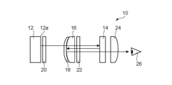
- FIG. 3 is a schematic diagram showing the general configuration of an example of a display system for VR goggles, and shows the arrangement and shape of each component of the display system.
- the display system 10 includes a display element 12, a reflective polarizing element 14, a first lens unit 16, a half mirror 18, a first ⁇ /4 element 20, a second ⁇ /4 element 22, and a second lens unit 24.
- the reflective polarizing element 14 is disposed in front of the display surface 12a of the display element 12, and can reflect light emitted from the display element 12.
- the first lens unit 16 is disposed on the optical path between the display element 12 and the reflective polarizing element 14, and the half mirror 18 is disposed between the display element 12 and the first lens unit 16.
- the first ⁇ /4 element 20 is disposed on the optical path between the display element 12 and the half mirror 18, and the second ⁇ /4 element 22 is disposed on the optical path between the half mirror 18 and the reflective polarizing element 14.
- the display element 12 is, for example, a liquid crystal display or an organic EL display, and has a display surface 12a for displaying an image.
- the light emitted from the display surface 12a passes through, for example, a polarizing member that may be included in the display element 12, and is converted into a first linearly polarized light.
- the first ⁇ /4 member 20 can convert the first linearly polarized light incident on the first ⁇ /4 member 20 into the first circularly polarized light.
- the first ⁇ /4 member 20 may be provided integrally with the display element 12.
- the half mirror 18 transmits the light emitted from the display element 12 and reflects the light reflected by the reflective polarizing element 14 toward the reflective polarizing element 14.
- the half mirror 18 is integrally provided with the first lens portion 16.
- the second ⁇ /4 member 22 can transmit the light reflected by the reflective polarizing member 14 and the half mirror 18 through the reflective polarizing member 14.
- the second ⁇ /4 member 22 may be integrally formed with the first lens portion 16.
- the first circularly polarized light emitted from the first ⁇ /4 member 20 passes through the half mirror 18 and the first lens portion 16, and is converted into the second linearly polarized light by the second ⁇ /4 member 22.
- the second linearly polarized light emitted from the second ⁇ /4 member 22 is reflected toward the half mirror 18 without passing through the reflective polarizing member 14.
- the polarization direction of the second linearly polarized light incident on the reflective polarizing member 14 is the same as the reflection axis of the reflective polarizing member 14. Therefore, the second linearly polarized light incident on the reflective polarizing member 14 is reflected by the reflective polarizing member 14.
- the second linearly polarized light reflected by the reflective polarizing element 14 is converted into a second circularly polarized light by the second ⁇ /4 element 22, and the second circularly polarized light emitted from the second ⁇ /4 element 22 passes through the first lens unit 16 and is reflected by the half mirror 18.
- the second circularly polarized light reflected by the half mirror 18 passes through the first lens unit 16 and is converted into a third linearly polarized light by the second ⁇ /4 element 22.
- the third linearly polarized light passes through the reflective polarizing element 14.
- the polarization direction of the third linearly polarized light incident on the reflective polarizing element 14 is the same as the transmission axis of the reflective polarizing element 14. Therefore, the third linearly polarized light incident on the reflective polarizing element 14 passes through the reflective polarizing element 14.
- the light that passes through the reflective polarizing member 14 passes through the second lens portion 24 and enters the user's eye 26.
- the absorption axis of the polarizing member included in the display element 12 and the reflection axis of the reflective polarizing member 14 may be arranged approximately parallel to each other or approximately perpendicular to each other.
- the angle between the absorption axis of the polarizing member included in the display element 12 and the slow axis of the first ⁇ /4 member 20 is, for example, 40° to 50°, may be 42° to 48°, or may be about 45°.
- the angle between the absorption axis of the polarizing member included in the display element 12 and the slow axis of the second ⁇ /4 member 22 is, for example, 40° to 50°, may be 42° to 48°, or may be about 45°.
- the in-plane phase difference Re(550) of the first ⁇ /4 member 20 is, for example, 100 nm to 190 nm, and may be 110 nm to 180 nm, 130 nm to 160 nm, or 135 nm to 155 nm.
- the first ⁇ /4 member 20 preferably exhibits an inverse dispersion wavelength characteristic in which the phase difference value increases according to the wavelength of the measurement light.
- the Re(450)/Re(550) of the first ⁇ /4 member 20 may be, for example, 0.75 or more and less than 1, or 0.8 or more and 0.95 or less.
- the in-plane phase difference Re(550) of the second ⁇ /4 member 22 is, for example, 100 nm to 190 nm, and may be 110 nm to 180 nm, 130 nm to 160 nm, or 135 nm to 155 nm.
- the second ⁇ /4 member 22 preferably exhibits an inverse dispersion wavelength characteristic in which the phase difference value increases according to the wavelength of the measurement light.
- the Re(450)/Re(550) of the second ⁇ /4 member 22 may be, for example, 0.75 or more and less than 1, or 0.8 or more and 0.95 or less.
- the display system 10 may also include an absorptive polarizing element disposed in front of the reflective polarizing element 14.
- the reflection axis of the reflective polarizing element and the absorption axis of the absorptive polarizing element may be disposed approximately parallel to each other.
- the optical film according to the embodiment of the present invention may include, for example, components provided in the display system.
- the optical film may include a polarizing component such as a reflective polarizing component or an absorptive polarizing component.
- the optical film may also include a phase difference component such as a ⁇ /4 component.
- the optical film may include other components such as a protective component, an adhesive layer for integrating adjacent components, a surface protective film, and a release liner.
- the thickness of the optical film may vary depending on, for example, the type and number of components included, but is, for example, 200 ⁇ m to 400 ⁇ m.
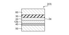
- FIG. 4 is a schematic cross-sectional view showing an example of the details of an optical film.
- FIG. 4 can also be a schematic cross-sectional view showing an example of the details of the optical film body before cutting.
- the optical film 2 includes a first ⁇ /4 member 20, a polarizing member 12b arranged on one side of the first ⁇ /4 member 20, and a protective member 30 arranged on the other side of the first ⁇ /4 member 20.
- the polarizing member 12b can correspond to the polarizing member that can be included in the display element (display element 12).
- An adhesive layer (e.g., a pressure-sensitive adhesive layer) 40 is provided on the polarizing member 12b side, and a release liner 50 is bonded to the surface of the adhesive layer 40.
- a surface protective film 60 is bonded to the surface of the protective member 30.
- the first ⁇ /4 member 20 preferably has a refractive index characteristic that satisfies the relationship nx>ny ⁇ nz.
- the Nz coefficient of the first ⁇ /4 member 20 is preferably 0.9 to 3, more preferably 0.9 to 2.5, even more preferably 0.9 to 1.5, and particularly preferably 0.9 to 1.3.
- the first ⁇ /4 member 20 is formed of any suitable material that can satisfy the above characteristics.
- the first ⁇ /4 member 20 can be, for example, a stretched resin film or an oriented and solidified layer of a liquid crystal compound.
- the resins contained in the resin film include polycarbonate-based resins, polyester carbonate-based resins, polyester-based resins, polyvinyl acetal-based resins, polyarylate-based resins, cyclic olefin-based resins, cellulose-based resins, polyvinyl alcohol-based resins, polyamide-based resins, polyimide-based resins, polyether-based resins, polystyrene-based resins, acrylic-based resins, and the like. These resins may be used alone or in combination. Methods for combining include blending and copolymerization, for example.
- a resin film containing a polycarbonate-based resin or a polyester carbonate-based resin (hereinafter sometimes simply referred to as a polycarbonate-based resin) may be suitably used.
- the polycarbonate-based resin any suitable polycarbonate-based resin can be used.
- the polycarbonate-based resin contains a structural unit derived from a fluorene-based dihydroxy compound, a structural unit derived from an isosorbide-based dihydroxy compound, and a structural unit derived from at least one dihydroxy compound selected from the group consisting of alicyclic diol, alicyclic dimethanol, di-, tri- or polyethylene glycol, and alkylene glycol or spiro glycol.
- the polycarbonate-based resin contains a structural unit derived from a fluorene-based dihydroxy compound, a structural unit derived from an isosorbide-based dihydroxy compound, a structural unit derived from an alicyclic dimethanol and/or a structural unit derived from a di-, tri- or polyethylene glycol; more preferably, it contains a structural unit derived from a fluorene-based dihydroxy compound, a structural unit derived from an isosorbide-based dihydroxy compound, and a structural unit derived from a di-, tri- or polyethylene glycol.
- the polycarbonate-based resin may contain structural units derived from other dihydroxy compounds as necessary.
- polycarbonate-based resins that can be suitably used for the first ⁇ /4 member 20 and methods for forming the first ⁇ /4 member 20 are described, for example, in JP 2014-10291 A, JP 2014-26266 A, JP 2015-212816 A, JP 2015-212817 A, and JP 2015-212818 A, and the descriptions in these publications are incorporated herein by reference.
- the thickness of the first ⁇ /4 member 20, which is made of a stretched resin film is, for example, 10 ⁇ m to 100 ⁇ m, preferably 10 ⁇ m to 70 ⁇ m, and more preferably 20 ⁇ m to 60 ⁇ m.
- the above-mentioned alignment solidified layer of the liquid crystal compound is a layer in which the liquid crystal compound is aligned in a predetermined direction within the layer, and the alignment state is fixed.
- the "alignment solidified layer” is a concept that includes an alignment solidified layer obtained by solidifying a liquid crystal monomer, as described below.
- rod-shaped liquid crystal compounds are aligned in the slow axis direction of the first ⁇ /4 member 20 (homogeneous alignment).
- rod-shaped liquid crystal compounds include liquid crystal polymers and liquid crystal monomers.
- the liquid crystal compound is preferably polymerizable. If the liquid crystal compound is polymerizable, the alignment state of the liquid crystal compound can be fixed by aligning the liquid crystal compound and then polymerizing it.
- the orientation solidified layer of the liquid crystal compound can be formed by performing an orientation treatment on the surface of a specified substrate, applying a coating liquid containing a liquid crystal compound to the surface to orient the liquid crystal compound in a direction corresponding to the orientation treatment, and fixing the orientation state.
- Any appropriate orientation treatment can be adopted as the orientation treatment.
- Specific examples include mechanical orientation treatment, physical orientation treatment, and chemical orientation treatment.
- Specific examples of mechanical orientation treatment include rubbing treatment and stretching treatment.
- Specific examples of physical orientation treatment include magnetic field orientation treatment and electric field orientation treatment.
- Specific examples of chemical orientation treatment include oblique deposition and photo-alignment treatment. Any appropriate conditions can be adopted as the processing conditions for the various orientation treatments depending on the purpose.
- the alignment of liquid crystal compounds is achieved by treating them at a temperature that exhibits a liquid crystal phase according to the type of liquid crystal compound. By carrying out such temperature treatment, the liquid crystal compounds take on a liquid crystal state, and the liquid crystal compounds are aligned according to the alignment treatment direction of the substrate surface.
- the alignment state is fixed by cooling the liquid crystal compound aligned as described above. If the liquid crystal compound is polymerizable or crosslinkable, the alignment state is fixed by subjecting the liquid crystal compound aligned as described above to a polymerization treatment or crosslinking treatment.
- liquid crystal compound any suitable liquid crystal polymer and/or liquid crystal monomer can be used as the liquid crystal compound.
- the liquid crystal polymer and the liquid crystal monomer can be used alone or in combination.
- Specific examples of liquid crystal compounds and methods for producing a liquid crystal alignment solidified layer are described in, for example, JP 2006-163343 A, JP 2006-178389 A, and WO 2018/123551 A. The descriptions in these publications are incorporated herein by reference.
- the thickness of the first ⁇ /4 member 20, which is composed of a liquid crystal alignment solidified layer is, for example, 1 ⁇ m to 10 ⁇ m, preferably 1 ⁇ m to 8 ⁇ m, more preferably 1 ⁇ m to 6 ⁇ m, and even more preferably 1 ⁇ m to 4 ⁇ m.
- the polarizing member 12b may include, for example, a resin film containing a dichroic material (sometimes referred to as an absorptive polarizing film).
- the thickness of the absorptive polarizing film is, for example, 1 ⁇ m or more and 20 ⁇ m or less, and may be 2 ⁇ m or more and 15 ⁇ m or less, 12 ⁇ m or less, 10 ⁇ m or less, 8 ⁇ m or less, or 5 ⁇ m or less.
- the absorptive polarizing film may be made from a single layer of resin film, or may be made using a laminate of two or more layers.
- an absorptive polarizing film When made from a single-layer resin film, for example, an absorptive polarizing film can be obtained by subjecting a hydrophilic polymer film such as a polyvinyl alcohol (PVA)-based film, a partially formalized PVA-based film, or an ethylene-vinyl acetate copolymer-based partially saponified film to a dyeing process using a dichroic substance such as iodine or a dichroic dye, a stretching process, etc.
- a hydrophilic polymer film such as a polyvinyl alcohol (PVA)-based film, a partially formalized PVA-based film, or an ethylene-vinyl acetate copolymer-based partially saponified film
- a dichroic substance such as iodine or a dichroic dye
- the dyeing with iodine is carried out, for example, by immersing the PVA-based film in an aqueous iodine solution.
- the stretching ratio of the uniaxial stretching is preferably 3 to 7 times. The stretching may be carried out after the dyeing process, or may be carried out while dyeing. Alternatively, the film may be stretched and then dyed. If necessary, the PVA-based film may be subjected to a swelling process, a crosslinking process, a washing process, a drying process, etc.
- examples of the laminate include a laminate of a resin substrate and a PVA-based resin layer (PVA-based resin film) laminated on the resin substrate, or a laminate of a resin substrate and a PVA-based resin layer formed by coating on the resin substrate.
- PVA-based resin film PVA-based resin film
- the absorptive polarizing film obtained using a laminate of a resin substrate and a PVA-based resin layer formed by coating on the resin substrate can be produced, for example, by applying a PVA-based resin solution to the resin substrate and drying to form a PVA-based resin layer on the resin substrate to obtain a laminate of the resin substrate and the PVA-based resin layer; and stretching and dyeing the laminate to make the PVA-based resin layer into an absorptive polarizing film.
- a polyvinyl alcohol-based resin layer containing a halide and a polyvinyl alcohol-based resin is formed on one side of the resin substrate.
- the stretching typically includes immersing the laminate in an aqueous boric acid solution and stretching it.
- the stretching may further include air-stretching the laminate at a high temperature (e.g., 95°C or higher) before stretching in the boric acid aqueous solution, if necessary.
- the laminate is preferably subjected to a drying shrinkage treatment in which the laminate is heated while being conveyed in the longitudinal direction, thereby shrinking the laminate by 2% or more in the width direction.
- the manufacturing method of this embodiment includes subjecting the laminate to an air-assisted stretching treatment, a dyeing treatment, an underwater stretching treatment, and a drying shrinkage treatment in this order.
- the obtained resin substrate/absorptive polarizing film laminate may be used as it is (i.e., the resin substrate may be used as a protective layer for the absorptive polarizing film), or any suitable protective layer may be laminated on the peeled surface obtained by peeling the resin substrate from the resin substrate/absorptive polarizing film laminate, or on the surface opposite to the peeled surface. Details of the manufacturing method of such an absorptive polarizing film are described in, for example, JP 2012-73580 A and JP 6470455 A. The entire disclosures of these publications are incorporated herein by reference.
- the crossed transmittance (Tc) of the polarizing member (absorptive polarizing film) is preferably 0.5% or less, more preferably 0.1% or less, and even more preferably 0.05% or less.
- the single transmittance (Ts) of the polarizing member (absorptive polarizing film) is, for example, 41.0% to 45.0%, and preferably 42.0% or more.
- the degree of polarization (P) of the polarizing member (absorptive polarizing film) is, for example, 99.0% to 99.997%, and preferably 99.9% or more.
- the crossed transmittance, single transmittance and degree of polarization can be measured, for example, using an ultraviolet-visible spectrophotometer.
- the degree of polarization P can be calculated by measuring the single transmittance Ts, parallel transmittance Tp and crossed transmittance Tc using an ultraviolet-visible spectrophotometer, and using the obtained Tp and Tc, according to the following formula.
- Ts, Tp and Tc are Y values measured using a 2-degree visual field (C light source) according to JIS Z 8701 and corrected for visibility.
- Polarization degree P (%) ⁇ (Tp-Tc)/(Tp+Tc) ⁇ 1/2 ⁇ 100
- the protective member 30 typically includes a substrate.
- the substrate may be made of any suitable film.
- Materials that are the main components of the film that constitutes the substrate include, for example, cellulose-based resins such as triacetyl cellulose (TAC), polyester-based, polyvinyl alcohol-based, polycarbonate-based, polyamide-based, polyimide-based, polyethersulfone-based, polysulfone-based, polystyrene-based, cycloolefin-based resins such as polynorbornene, polyolefin-based, (meth)acrylic, acetate-based resins, and the like.
- the thickness of the substrate is preferably 5 ⁇ m to 80 ⁇ m, more preferably 10 ⁇ m to 40 ⁇ m, and even more preferably 15 ⁇ m to 35 ⁇ m.
- the protective member 30 may preferably have a substrate and a surface treatment layer formed on the substrate.
- the protective member having a surface treatment layer may be arranged so that the substrate is located on the first ⁇ /4 member 20 side.
- the surface treatment layer may have any appropriate function.
- the surface treatment layer preferably has an anti-reflection function.
- the thickness of the surface treatment layer is preferably 1 ⁇ m to 20 ⁇ m, more preferably 2 ⁇ m to 15 ⁇ m, and even more preferably 3 ⁇ m to 10 ⁇ m.
- the positive C plate has a thickness direction retardation Rth(550) of preferably -50 nm to -300 nm, more preferably -70 nm to -250 nm, even more preferably -90 nm to -200 nm, and particularly preferably -100 nm to -180 nm.
- Rth(550) preferably -50 nm to -300 nm, more preferably -70 nm to -250 nm, even more preferably -90 nm to -200 nm, and particularly preferably -100 nm to -180 nm.
- the positive C plate may be made of any suitable material, but is preferably made of a film containing a liquid crystal material fixed in homeotropic alignment.
- the liquid crystal material (liquid crystal compound) that can be homeotropically aligned may be a liquid crystal monomer or a liquid crystal polymer.
- Specific examples of such liquid crystal compounds and methods for forming a positive C plate include the liquid crystal compounds and methods for forming the retardation layer described in [0020] to [0028] of JP 2002-333642 A.
- the thickness of the positive C plate is preferably 0.5 ⁇ m to 5 ⁇ m.
- the release liner 50 is formed of any suitable resin film.
- suitable resin film examples include polyethylene terephthalate (PET), polyethylene, and polypropylene.
- PET polyethylene terephthalate
- the resin film materials can be used alone or in combination.
- the surface of the release liner 50 that comes into contact with the adhesive layer 40 may be provided with a release treatment layer.
- release treatment agents that form the release treatment layer include silicone-based release treatment agents, fluorine-based release treatment agents, and long-chain alkyl acrylate-based release agents. These can be used alone or in combination.
- the thickness of the release treatment layer is typically 50 nm or more and 400 nm or less.
- the thickness of the release liner is, for example, 5 ⁇ m or more and 60 ⁇ m or less, and preferably 20 ⁇ m or more and 45 ⁇ m or less. When a release treatment layer is applied, the thickness of the release liner includes the thickness of the release treatment layer.
- the surface protection film 60 is typically a laminate of a base film and an adhesive layer.
- Materials for forming the base film include polyester-based polymers such as polyethylene terephthalate (PET), polyethylene naphthalate (PEN), polybutylene terephthalate (PBT), etc.; cellulose-based polymers such as diacetyl cellulose and triacetyl cellulose; polycarbonate-based polymers; (meth)acrylic polymers such as polymethyl methacrylate; and cycloolefin-based polymers such as polynorbornene. These may be used alone or in combination of two or more.
- the thickness of the base film is, for example, 5 ⁇ m or more and 200 ⁇ m or less, and preferably 20 ⁇ m or more and 100 ⁇ m or less.
- any suitable structure may be adopted for the adhesive layer of the laminate.
- Specific examples include acrylic adhesives, rubber adhesives, silicone adhesives, polyester adhesives, urethane adhesives, epoxy adhesives, and polyether adhesives.
- an adhesive having the desired properties according to the purpose can be prepared.
- the base resin of the adhesive may be used alone or in combination of two or more types.
- the base resin is preferably an acrylic resin (specifically, the adhesive layer is preferably composed of an acrylic adhesive).
- the thickness of the adhesive layer is, for example, 5 ⁇ m to 15 ⁇ m.
- each member included in the optical film is preferably integrated via an adhesive layer.
- the adhesive layer may be formed of an adhesive or a pressure-sensitive adhesive.
- the thickness of the adhesive layer is, for example, 0.05 ⁇ m to 30 ⁇ m, preferably 3 ⁇ m to 20 ⁇ m, and more preferably 5 ⁇ m to 15 ⁇ m.
- the thickness, retardation value and peel strength were measured by the following measuring methods.
- ⁇ Phase difference value> The phase difference value at each wavelength at 23° C. was measured using a Mueller matrix polarimeter (manufactured by Axometrics, product name "Axoscan”).
- the peel strength was measured by laminating a sample cut to a size of 25 mm wide and 150 mm long to a glass plate, and then peeling the sample in the length direction at a peel speed of 300 mm/min and a peel angle of 90° using a universal tensile tester, and measuring the peel strength (N/25 mm) in an environment of 23° C. and 50% RH. The same sample was measured five times, and the average value was calculated.
- Example 1 (Fabrication of ⁇ /4 Members) Polymerization was carried out using a batch polymerization apparatus consisting of two vertical reactors equipped with stirring blades and a reflux condenser controlled at 100°C. 29.60 parts by mass (0.046 mol) of bis[9-(2-phenoxycarbonylethyl)fluoren-9-yl]methane, 29.21 parts by mass (0.200 mol) of isosorbide (ISB), 42.28 parts by mass (0.139 mol) of spiroglycol (SPG), 63.77 parts by mass (0.298 mol) of diphenyl carbonate (DPC), and 1.19 x 10 -2 parts by mass (6.78 x 10 -5 mol) of calcium acetate monohydrate as a catalyst were charged.
- ISB isosorbide
- SPG spiroglycol
- DPC diphenyl carbonate
- the obtained polyester carbonate resin (pellets) was vacuum dried at 80°C for 5 hours, and then a long resin film with a thickness of 135 ⁇ m was produced using a film-making device equipped with a single-screw extruder (manufactured by Toshiba Machine Co., Ltd., cylinder set temperature: 250°C), a T-die (width 200 mm, set temperature: 250°C), a chill roll (set temperature: 120-130°C) and a winder.
- the obtained long resin film was stretched in the width direction at a stretching temperature of 143°C and a stretching ratio of 2.8 times to obtain a stretched film with a thickness of 47 ⁇ m.
- the Re(550) of the obtained stretched film was 143 nm, Re(450)/Re(550) was 0.86, and the Nz coefficient was 1.12.
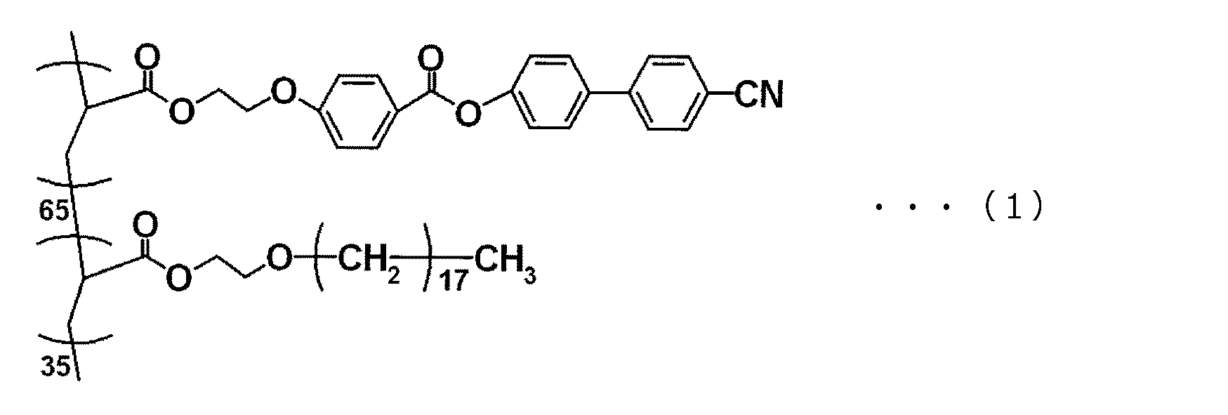
- a liquid crystal coating liquid was prepared by dissolving 20 parts by weight of a side-chain liquid crystal polymer represented by the following chemical formula (1) (the numbers 65 and 35 in the formula indicate the mol% of the monomer unit, and are conveniently represented as a block polymer: weight average molecular weight 5000), 80 parts by weight of a polymerizable liquid crystal exhibiting a nematic liquid crystal phase (manufactured by BASF: trade name Paliocolor LC242), and 5 parts by weight of a photopolymerization initiator (manufactured by Ciba Specialty Chemicals: trade name Irgacure 907) in 200 parts by weight of cyclopentanone.
- a side-chain liquid crystal polymer represented by the following chemical formula (1) (the numbers 65 and 35 in the formula indicate the mol% of the monomer unit, and are conveniently represented as a block polymer: weight average molecular weight 5000), 80 parts by weight of a polymerizable liquid crystal exhibiting a nematic liquid crystal phase (
- the coating liquid was applied to a PET substrate that had been subjected to a vertical alignment treatment by a bar coater, and the liquid crystal was aligned by heating and drying at 80°C for 4 minutes.
- This liquid crystal layer was irradiated with ultraviolet light to harden the liquid crystal layer, thereby forming a positive C plate having a thickness of 4 ⁇ m and an Rth (550) of ⁇ 100 nm on the substrate.
- the following hard coat layer-forming material was applied to an acrylic film (thickness 40 ⁇ m) having a lactone ring structure, and heated at 90° C. for 1 minute. After heating, the coating layer was irradiated with ultraviolet light from a high-pressure mercury lamp at an integrated light quantity of 300 mJ/ cm2 to harden the coating layer, thereby producing an acrylic film (thickness 44 ⁇ m) on which a hard coat layer having a thickness of 4 ⁇ m was formed. Next, the following coating solution A for forming an antireflection layer was applied onto the hard coat layer using a wire bar, and the applied coating solution was heated at 80° C. for 1 minute and dried to form a coating film.
- the dried coating film was irradiated with ultraviolet light from a high-pressure mercury lamp at an integrated light quantity of 300 mJ/cm 2 to cure the coating film, forming an antireflection layer A having a thickness of 140 nm.
- the following coating solution B for forming an antireflection layer was applied onto the antireflection layer A with a wire bar, and the applied coating solution was heated at 80° C. for 1 minute and dried to form a coating film.
- the dried coating film was irradiated with ultraviolet rays from a high-pressure mercury lamp at an integrated light quantity of 300 mJ/ cm2 to cure the coating film, thereby forming an antireflection layer B with a thickness of 105 nm. In this way, a protective member (thickness: 44 ⁇ m) was obtained.
- a hard coat layer-forming material was prepared by mixing 50 parts by weight of a urethane acrylic oligomer (manufactured by Shin-Nakamura Chemical Co., Ltd., "NK Oligo UA-53H”), 30 parts by weight of a multifunctional acrylate mainly composed of pentaerythritol triacrylate (manufactured by Osaka Organic Chemical Industry Co., Ltd., product name "Viscoat #300”), 20 parts by weight of 4-hydroxybutyl acrylate (manufactured by Osaka Organic Chemical Industry Co., Ltd.), 1 part by weight of a leveling agent (manufactured by DIC Corporation, "GRANDIC PC4100”) and 3 parts by weight of a photopolymerization initiator (manufactured by Ciba Japan KK, "Irgacure 907”) and diluting with methyl isobutyl ketone to a solids concentration of 50% by weight.
- a urethane acrylic oligomer
- Coating liquid A for forming antireflection layer 100 parts by weight of a multifunctional acrylate (manufactured by Arakawa Chemical Industries, Ltd., product name “Opstar KZ6728", solid content 20% by weight), 3 parts by weight of a leveling agent (manufactured by DIC Corporation, "GRANDIC PC4100"), and a photopolymerization initiator (The mixture was diluted with butyl acetate as a diluting solvent to a solid content of 12% by weight, and the mixture was stirred and subjected to a reflection. A coating solution A for forming a protective layer was prepared.
- Coating liquid B for forming antireflection layer 100 parts by weight of a polyfunctional acrylate containing pentaerythritol triacrylate as the main component (manufactured by Osaka Organic Chemical Industry Co., Ltd., product name "Viscoat #300", solid content 100% by weight), hollow nanosilica particles (JGC Catalysts and Chemicals Co., Ltd.
- Solid nanosilica particles manufactured by Nissan Chemical Industries, Ltd., product name "Surulia 5320", solid content 20% by weight, weight average particle diameter 75 nm), %, weight average particle size 10 nm
- fluorine-containing additive manufactured by Shin-Etsu Chemical Co., Ltd., product name "KY-1203", solid content 20% by weight
- a photopolymerization initiator BASF's product name "OMNIRAD907” (solid content 100 wt.) was mixed with 3 parts by weight.
- thermoplastic resin substrate As a thermoplastic resin substrate, a long amorphous isophthalic copolymerized polyethylene terephthalate film (thickness: 100 ⁇ m) having a Tg of about 75° C. was used, and one side of the resin substrate was subjected to a corona treatment.
- a PVA aqueous solution (coating solution) was prepared by adding 13 parts by weight of potassium iodide to 100 parts by weight of a PVA-based resin prepared by mixing polyvinyl alcohol (polymerization degree 4,200, saponification degree 99.2 mol%) and acetoacetyl-modified PVA (manufactured by Mitsubishi Chemical Corporation, product name "GOHSENEX Z410") in a ratio of 9:1, and dissolving the resultant in water.
- the above PVA aqueous solution was applied to the corona-treated surface of a resin substrate and dried at 60° C. to form a PVA-based resin layer having a thickness of 13 ⁇ m, thereby producing a laminate.
- the obtained laminate was uniaxially stretched 2.4 times in the machine direction (longitudinal direction) in an oven at 130° C. (auxiliary in-air stretching treatment).
- the laminate was immersed in an insolubilizing bath (a boric acid aqueous solution obtained by mixing 4 parts by weight of boric acid with 100 parts by weight of water) at a liquid temperature of 40° C. for 30 seconds (insolubilizing treatment).
- the film was immersed in a dye bath (an aqueous iodine solution obtained by mixing iodine and potassium iodide in a weight ratio of 1:7 with respect to 100 parts by weight of water) having a liquid temperature of 30° C.
- the plate was immersed in a crosslinking bath (a boric acid aqueous solution obtained by mixing 3 parts by weight of potassium iodide and 5 parts by weight of boric acid with 100 parts by weight of water) at a liquid temperature of 40° C. for 30 seconds (crosslinking treatment).
- a crosslinking bath a boric acid aqueous solution obtained by mixing 3 parts by weight of potassium iodide and 5 parts by weight of boric acid with 100 parts by weight of water
- the laminate was immersed in an aqueous boric acid solution (boric acid concentration: 4 wt %, potassium iodide concentration: 5 wt %) at a liquid temperature of 70° C., and uniaxially stretched in the longitudinal direction (longitudinal direction) between rolls with different peripheral speeds to a total stretch ratio of 5.5 times (underwater stretching treatment). Thereafter, the laminate was immersed in a cleaning bath (an aqueous solution obtained by mixing 4 parts by weight of potassium iodide with 100 parts by weight of water) at a liquid temperature of 20° C. (cleaning treatment).
- a cleaning bath an aqueous solution obtained by mixing 4 parts by weight of potassium iodide with 100 parts by weight of water
- the laminate was brought into contact with a SUS heated roll whose surface temperature was maintained at about 75° C. (drying shrinkage treatment).
- the shrinkage rate of the laminate in the width direction due to the drying shrinkage treatment was 5.2%.
- an absorptive polarizing film having a thickness of about 5 ⁇ m was formed on the resin substrate.
- a cycloolefin resin film (thickness: 25 ⁇ m) was attached as a protective layer to the surface of the obtained absorptive polarizing film (the surface opposite to the resin substrate) via an ultraviolet-curable adhesive.
- the curable adhesive was applied so that the total thickness was about 1 ⁇ m, and the two were attached using a rolling machine.
- the adhesive was cured by irradiating it with UV light from the cycloolefin resin film side. Then, the resin substrate was peeled off. This resulted in a polarizing member having a cycloolefin resin film/absorptive polarizing film structure.
- the polarizing member had a single transmittance (Ts) of 43.4% and a polarization degree of 99.993%.
- an acrylic polymer having a weight average molecular weight (Mw) of 2.2 million was prepared.
- An acrylic adhesive was prepared by blending 0.6 parts by weight of a trimethylolpropane/tolylene diisocyanate adduct (product name: Coronate L, manufactured by Tosoh Corporation) and 0.075 parts by weight of a silane coupling agent (product name: KBM403, manufactured by Shin-Etsu Chemical Co., Ltd.) with 100 parts by weight of the solid content of the obtained acrylic polymer solution.
- the obtained acrylic pressure-sensitive adhesive composition was applied to a substrate film and dried to form a pressure-sensitive adhesive layer having a thickness of 12 ⁇ m and a pressure-sensitive adhesive layer having a thickness of 15 ⁇ m.
- an isocyanurate of hexamethylene diisocyanate (“Coronate HX" manufactured by Tosoh Corporation)
- 3 parts by mass (solid content 0.03 parts by mass) of dibutyltin dilaurate (1% by mass solution in ethyl acetate) as a crosslinking catalyst were added to 500 parts by mass (
- ⁇ Surface Protection Film A> The adhesive composition A was applied to one side of a substrate (PET film, "CE905-38" manufactured by KOLON Corporation, thickness 38 ⁇ m) and then dried to form an adhesive layer (thickness 15 ⁇ m). Next, a release liner (manufactured by Toyobo Co., Ltd., product number TG704) was attached to the surface of the adhesive layer opposite the substrate. Thus, a surface protection film A was obtained.
- a surface protection film C was obtained in the same manner as in Production Example 1A, except that a PET film ("Part No. T100C38" manufactured by Mitsubishi Chemical Corporation, thickness 38 ⁇ m) was used as the substrate and adhesive composition A was applied to its corona-treated surface to form an adhesive layer having a thickness of 5 ⁇ m.
- the positive C plate was attached to the ⁇ /4 member (stretched film) via an ultraviolet-curing adhesive (thickness after curing: 1 ⁇ m) to obtain a retardation member.
- the protective member (acrylic film having a hard coat layer and an antireflection layer formed thereon) was attached to the positive C plate side of the obtained retardation member via the pressure-sensitive adhesive layer (thickness: 12 ⁇ m).
- the acrylic film of the protective member was attached to the positive C plate side.
- the surface protective film A and the surface protective film C were attached to the antireflection layer side of the protective member in this order after removing the release liners.
- the polarizing member was attached to the ⁇ /4 member side of the retardation member via the pressure-sensitive adhesive layer (thickness: 12 ⁇ m).
- the lamination was performed so that the angle between the slow axis of the ⁇ /4 member and the absorption axis of the absorptive polarizing film was 45°.
- the polarizing member was also attached so that the absorptive polarizing film was located on the ⁇ /4 member side.
- the pressure-sensitive adhesive layer (thickness: 15 ⁇ m) was attached to the cycloolefin resin film side of the polarizing member, and a release liner (manufactured by Toyobo Co., Ltd., product number TG704) was attached. In this way, a laminated film having a thickness of 330 ⁇ m was obtained.
- a tape (acrylic adhesive tape with a substrate) with a peel strength of 3.5 N/25 mm was attached to the cut surface of the workpiece and then peeled off. This operation was continued until no fuzz generated by cutting was visible. Thus, an optical film was obtained.
- Example 2 An optical film was obtained in the same manner as in Example 1, except that the rotation speed of the end mill in cutting was set to 3000 rpm.
- Example 3 An optical film was obtained in the same manner as in Example 1, except that the rotation speed of the end mill in cutting was set to 6000 rpm.
- An adhesive film with a peeling force of 3.5 N/25 mm and a size of 30 mm x 30 mm was attached to the end surface of the optical film of the example and comparative example. Specifically, the adhesive film was attached to the cutting surface of the workpiece while 20 sheets were stacked. The adhesive film was then peeled off from the end surface of the optical film, and the number of foreign objects attached to the adhesive surface of the adhesive film was counted using a surface cleanliness particle monitor (PartSens manufactured by Intechnos Japan Co., Ltd.).
- the present invention is not limited to the above-described embodiment, and various modifications are possible.
- the configurations shown in the above-described embodiments can be replaced with configurations that are substantially the same as those shown in the above-described embodiments, that have the same effects, or that can achieve the same purpose.
- optical film according to the embodiment of the present invention can be used in image display devices, and can be suitably used in, for example, VR goggles.
Landscapes
- Engineering & Computer Science (AREA)
- Mechanical Engineering (AREA)
- Physics & Mathematics (AREA)
- Health & Medical Sciences (AREA)
- Manufacturing & Machinery (AREA)
- Ophthalmology & Optometry (AREA)
- General Physics & Mathematics (AREA)
- Optics & Photonics (AREA)
- Chemical & Material Sciences (AREA)
- Organic Chemistry (AREA)
- Polarising Elements (AREA)
- Surface Treatment Of Optical Elements (AREA)
Abstract
Description
2.上記1に記載の光学フィルムの製造方法において、上記少なくとも1つの光学フィルム本体は、複数の光学フィルム本体を含み、上記複数の光学フィルム本体を重ねた状態で、上記加工を行ってもよい。
3.上記1または2に記載の光学フィルムの製造方法において、上記加工面の厚み方向と直交する方向の単位長さ10mm当たりの長径50μmを超え150μm以下の異物の量が10個以下の光学フィルムを得てもよい。
4.上記1から3のいずれかに記載の光学フィルムの製造方法において、上記除去は、テープを用いて行ってもよい。
5.上記4に記載の光学フィルムの製造方法において、上記除去は、上記テープを上記加工面に貼り付けて剥がす操作を複数回行うことを含んでもよい。
6.上記4または5に記載の光学フィルムの製造方法において、上記テープの剥離力は、2N/25mm以上10N/25mm以下であってもよい。
7.上記1から6のいずれかに記載の光学フィルムの製造方法において、上記除去は、上記加工面に気体を吹き付けて行ってもよい。
本明細書における用語および記号の定義は下記の通りである。
(1)屈折率(nx、ny、nz)
「nx」は面内の屈折率が最大になる方向(すなわち、遅相軸方向)の屈折率であり、「ny」は面内で遅相軸と直交する方向(すなわち、進相軸方向)の屈折率であり、「nz」は厚み方向の屈折率である。
(2)面内位相差(Re)
「Re(λ)」は、23℃における波長λnmの光で測定した面内位相差である。例えば、「Re(550)」は、23℃における波長550nmの光で測定した面内位相差である。Re(λ)は、層(フィルム)の厚みをd(nm)としたとき、式:Re(λ)=(nx-ny)×dによって求められる。
(3)厚み方向の位相差(Rth)
「Rth(λ)」は、23℃における波長λnmの光で測定した厚み方向の位相差である。例えば、「Rth(550)」は、23℃における波長550nmの光で測定した厚み方向の位相差である。Rth(λ)は、層(フィルム)の厚みをd(nm)としたとき、式:Rth(λ)=(nx-nz)×dによって求められる。
(4)Nz係数
Nz係数は、Nz=Rth/Reによって求められる。
(5)角度
本明細書において角度に言及するときは、当該角度は基準方向に対して時計回りおよび反時計回りの両方を包含する。したがって、例えば「45°」は±45°を意味する。
偏光度P(%)={(Tp-Tc)/(Tp+Tc)}1/2×100
<厚み>
10μm以下の厚みは、走査型電子顕微鏡(日本電子社製、製品名「JSM-7100F」)を用いて測定した。10μmを超える厚みは、デジタルマイクロメーター(アンリツ社製、製品名「KC-351C」)を用いて測定した。
<位相差値>
ミュラーマトリクス・ポラリメーター(Axometrics社製、製品名「Axoscan」)を用いて、23℃における各波長での位相差値を測定した。
<剥離力>
剥離力は、幅25mm、長さ150mmのサイズに切り出したサンプルをガラス板に貼り合わせた後、サンプルを万能引張試験機にて剥離速度300mm/分、剥離角度90°で長さ方向に剥離したときの剥離力(N/25mm)を、23℃、50%RHの環境下で測定した。なお、同じサンプルに対し5回測定を行い、平均値を算出した。
(λ/4部材の作製)
撹拌翼および100℃に制御された還流冷却器を具備した縦型反応器2器からなるバッチ重合装置を用いて重合を行った。ビス[9-(2-フェノキシカルボニルエチル)フルオレン-9-イル]メタン29.60質量部(0.046mol)、イソソルビド(ISB)29.21質量部(0.200mol)、スピログリコール(SPG)42.28質量部(0.139mol)、ジフェニルカーボネート(DPC)63.77質量部(0.298mol)及び触媒として酢酸カルシウム1水和物1.19×10⁻²質量部(6.78×10⁻⁵mol)を仕込んだ。反応器内を減圧窒素置換した後、熱媒で加温を行い、内温が100℃になった時点で撹拌を開始した。昇温開始40分後に内温を220℃に到達させ、この温度を保持するように制御すると同時に減圧を開始し、220℃に到達してから90分で13.3kPaにした。重合反応とともに副生するフェノール蒸気を100℃の還流冷却器に導き、フェノール蒸気中に若干量含まれるモノマー成分を反応器に戻し、凝縮しないフェノール蒸気は45℃の凝縮器に導いて回収した。第1反応器に窒素を導入して一旦大気圧まで復圧させた後、第1反応器内のオリゴマー化された反応液を第2反応器に移した。次いで、第2反応器内の昇温および減圧を開始して、50分で内温240℃、圧力0.2kPaにした。その後、所定の攪拌動力となるまで重合を進行させた。所定動力に到達した時点で反応器に窒素を導入して復圧し、生成したポリエステルカーボネート系樹脂を水中に押し出し、ストランドをカッティングしてペレットを得た。
下記化学式(1)(式中の数字65および35はモノマーユニットのモル%を示し、便宜的にブロックポリマー体で表している:重量平均分子量5000)で示される側鎖型液晶ポリマー20重量部、ネマチック液晶相を示す重合性液晶(BASF社製:商品名PaliocolorLC242)80重量部および光重合開始剤(チバスペシャリティーケミカルズ社製:商品名イルガキュア907)5重量部をシクロペンタノン200重量部に溶解して液晶塗工液を調製した。そして、垂直配向処理を施したPET基材に当該塗工液をバーコーターにより塗工した後、80℃で4分間加熱乾燥することによって液晶を配向させた。この液晶層に紫外線を照射し、液晶層を硬化させることにより、厚みが4μm、Rth(550)が-100nmのポジティブCプレートを基材上に形成した。
ラクトン環構造を有するアクリルフィルム(厚み40μm)に、下記のハードコート層形成材料を塗布して90℃で1分間加熱し、加熱後の塗布層に高圧水銀ランプにて積算光量300mJ/cm2の紫外線を照射して塗布層を硬化させ、厚み4μmのハードコート層が形成されたアクリルフィルム(厚み44μm)を作製した。
次いで、上記ハードコート層上に、下記の反射防止層形成用塗工液Aをワイヤーバーで塗工し、塗工した塗工液を80℃で1分間加熱し、乾燥させて塗膜を形成した。乾燥後の塗膜に、高圧水銀ランプにて積算光量300mJ/cm2の紫外線を照射して塗膜を硬化させ、厚み140nmの反射防止層Aを形成した。
続いて、反射防止層A上に、下記の反射防止層形成用塗工液Bをワイヤーバーで塗工し、塗工した塗工液を80℃で1分間加熱し、乾燥させて塗膜を形成した。乾燥後の塗膜に、高圧水銀ランプにて積算光量300mJ/cm2の紫外線を照射して塗膜を硬化させ、厚み105nmの反射防止層Bを形成した。
こうして、保護部材(厚み44μm)を得た。
ウレタンアクリルオリゴマー(新中村化学社製、「NKオリゴ UA-53H」)50重量部、ペンタエリストールトリアクリレートを主成分とする多官能アクリレート(大阪有機化学工業社製、商品名「ビスコート#300」)30重量部、4-ヒドロキシブチルアクリレート(大阪有機化学工業社製)20重量部、レベリング剤(DIC社製、「GRANDIC PC4100」)1重量部および光重合開始剤(チバ・ジャパン社製、「イルガキュア907」)3重量部を混合し、固形分濃度が50重量%になるようにメチルイソブチルケトンで希釈して、ハードコート層形成材料を調製した。
多官能アクリレート(荒川化学工業株式会社製、商品名「オプスターKZ6728」、固形分20重量%)100重量部、レベリング剤(DIC社製、「GRANDIC PC4100」)3重量部、および光重合開始剤(BASF社製、商品名「OMNIRAD907」、固形分100重量%)3重量部を混合した。その混合物に、希釈溶媒として酢酸ブチルを用いて固形分が12重量%となるようにし、攪拌して反射防止層形成用塗工液Aを調製した。
ペンタエリストールトリアクリレートを主成分とする多官能アクリレート(大阪有機化学工業株式会社製、商品名「ビスコート#300」、固形分100重量%)100重量部、中空ナノシリカ粒子(日揮触媒化成工業株式会社製、商品名「スルーリア5320」、固形分20重量%、重量平均粒子径75nm)150重量部、中実ナノシリカ粒子(日産化学工業株式会社製、商品名「MEK-2140Z-AC」、固形分30重量%、重量平均粒子径10nm)50重量部、フッ素元素含有添加剤(信越化学工業株式会社製、商品名「KY-1203」、固形分20重量%)12重量部、および光重合開始剤(BASF社製、商品名「OMNIRAD907」、固形分100重量%)3重量部を混合した。その混合物に、希釈溶媒としてTBA(ターシャリーブチルアルコール)、MIBK(メチルイソブチルケトン)およびPMA(プロピレングリコールモノメチルエーテルアセテート)を60:25:15重量比で混合した混合溶媒を添加して全体の固形分が4重量%となるようにし、攪拌して反射防止層形成用塗工液Bを調製した。
熱可塑性樹脂基材として、長尺状で、Tg約75℃である、非晶質のイソフタル共重合ポリエチレンテレフタレートフィルム(厚み:100μm)を用い、樹脂基材の片面に、コロナ処理を施した。
ポリビニルアルコール(重合度4200、ケン化度99.2モル%)およびアセトアセチル変性PVA(三菱ケミカル社製、商品名「ゴーセネックスZ410」)を9:1で混合したPVA系樹脂100重量部に、ヨウ化カリウム13重量部を添加したものを水に溶かし、PVA水溶液(塗布液)を調製した。
樹脂基材のコロナ処理面に、上記PVA水溶液を塗布して60℃で乾燥することにより、厚み13μmのPVA系樹脂層を形成し、積層体を作製した。
得られた積層体を、130℃のオーブン内で縦方向(長手方向)に2.4倍に一軸延伸した(空中補助延伸処理)。
次いで、積層体を、液温40℃の不溶化浴(水100重量部に対して、ホウ酸を4重量部配合して得られたホウ酸水溶液)に30秒間浸漬させた(不溶化処理)。
次いで、液温30℃の染色浴(水100重量部に対して、ヨウ素とヨウ化カリウムを1:7の重量比で配合して得られたヨウ素水溶液)に、最終的に得られる吸収型偏光膜の単体透過率(Ts)が所望の値となるように濃度を調整しながら60秒間浸漬させた(染色処理)。
次いで、液温40℃の架橋浴(水100重量部に対して、ヨウ化カリウムを3重量部配合し、ホウ酸を5重量部配合して得られたホウ酸水溶液)に30秒間浸漬させた(架橋処理)。
その後、積層体を、液温70℃のホウ酸水溶液(ホウ酸濃度4重量%、ヨウ化カリウム濃度5重量%)に浸漬させながら、周速の異なるロール間で縦方向(長手方向)に総延伸倍率が5.5倍となるように一軸延伸を行った(水中延伸処理)。
その後、積層体を液温20℃の洗浄浴(水100重量部に対して、ヨウ化カリウムを4重量部配合して得られた水溶液)に浸漬させた(洗浄処理)。
その後、約90℃に保たれたオーブン中で乾燥しながら、表面温度が約75℃に保たれたSUS製の加熱ロールに接触させた(乾燥収縮処理)。乾燥収縮処理による積層体の幅方向の収縮率は5.2%であった。
このようにして、樹脂基材上に厚み約5μmの吸収型偏光膜を形成した。
得られた吸収型偏光膜の表面(樹脂基材とは反対側の面)に、保護層としてのシクロオレフィン系樹脂フィルム(厚み:25μm)を、紫外線硬化型接着剤を介して貼り合わせた。具体的には、硬化型接着剤の総厚みが約1μmになるように塗工し、ロール機を使用して貼り合わせた。その後、UV光線をシクロオレフィン系樹脂フィルム側から照射して接着剤を硬化させた。次いで、樹脂基材を剥離した。
これによって、シクロオレフィン系樹脂フィルム/吸収型偏光膜の構成を有する偏光部材を得た。偏光部材の単体透過率(Ts)は43.4%であり、偏光度は99.993%であった。
攪拌羽根、温度計、窒素ガス導入管および冷却器を備えた4つ口フラスコに、ブチルアクリレート94.9重量部、アクリル酸5重量部および2-ヒドロキシエチルアクリレート0.1重量部を含有するモノマー混合物を仕込んだ。さらに、このモノマー混合物100重量部に対して、重合開始剤としてジベンゾイルパーオキシド0.3重量部を酢酸エチルと共に仕込み、緩やかに攪拌しながら窒素ガスを導入してフラスコ内を窒素置換した後、フラスコ内の液温を60℃に保って7時間重合反応を行った。次いで、得られた反応液に酢酸エチルを加えて固形分濃度30重量%に調整し、重量平均分子量(Mw)220万のアクリル系ポリマーの溶液を調製した。
得られたアクリル系ポリマー溶液の固形分100重量部に対して、トリメチロールプロパン/トリレンジイソシアネート付加物(商品名:コロネートL、東ソー社製)0.6重量部と、シランカップリング剤(商品名:KBM403、信越化学工業社製)0.075重量部を配合して、アクリル系粘着剤を調製した。
得られたアクリル系粘着剤組成物を基材フィルムに塗工して乾燥し、厚みが12μmの粘着剤層および厚みが15μmの粘着剤層を形成した。
<アクリルポリマーA>
温度計、攪拌機、冷却器および窒素ガス導入管を備える反応容器内に、モノマー成分として、2-エチルヘキシルアクリレート(2EHA)96.2質量部、およびヒドロキシエチルアクリレート(HEA)3.8質量部、ならびに重合開始剤として2,2’-アゾビスイソブチロニトリル(AIBN)0.2質量部を酢酸エチル150質量部とともに仕込み、23℃で緩やかに攪拌しながら窒素ガスを導入して窒素置換を行った。その後、液温を65℃付近に保って6時間重合反応を行い、アクリルポリマーAの溶液(濃度40質量%)を調製した。アクリルポリマーAの重量平均分子量は54万であった。
アクリルポリマーAの溶液に酢酸エチルを加えて濃度20質量%に希釈した。この溶液500質量部(固形分100質量部)に、架橋剤としてヘキサメチレンジイソシアネートのイソシアヌレート体(東ソー社製「コロネートHX」)4質量部、および架橋触媒としてジラウリン酸ジブチルスズ(1質量%酢酸エチル溶液)3質量部(固形分0.03質量部)を加えて攪拌し、粘着剤組成物Aを調製した。
基材(PETフィルム、KOLON社製「CE905-38」、厚み38μm)の片面に、粘着剤組成物Aを塗布し、その後乾燥させて粘着剤層(厚み15μm)を形成した。次いで、粘着剤層の基材と反対側の表面に、はく離ライナー(東洋紡社製、品番TG704)を貼り付けた。これにより表面保護フィルムAを得た。
基材としてPETフィルム(三菱ケミカル社製「品番T100C38」、厚み38μm)を用い、そのコロナ処理面に粘着剤組成物Aを塗布して厚み5μmの粘着剤層を形成したこと以外は製造例1Aと同様にして表面保護フィルムCを得た。
上記λ/4部材(延伸フィルム)に紫外線硬化型接着剤(硬化後の厚み1μm)を介して上記ポジティブCプレートを貼り合わせて、位相差部材を得た。
得られた位相差部材のポジティブCプレート側に、上記粘着剤層(厚み:12μm)を介して上記保護部材(ハードコート層および反射防止層が形成されたアクリルフィルム)を貼り合わせた。ここで、保護部材のアクリルフィルムがポジティブCプレート側に位置するように貼り合わせた。そして、保護部材の反射防止層側に、上記表面保護フィルムAおよび表面保護フィルムCを、それぞれはく離ライナーを剥がして、この順に貼り合わせた。
次いで、位相差部材のλ/4部材側に、上記粘着剤層(厚み:12μm)を介して、上記偏光部材を貼り合わせた。ここで、λ/4部材の遅相軸と吸収型偏光膜の吸収軸とのなす角度が45°となるように貼り合わせた。また、偏光部材の吸収型偏光膜がλ/4部材側に位置するように貼り合わせた。そして、偏光部材のシクロオレフィン系樹脂フィルム側に、上記粘着剤層(厚み:15μm)を貼り合わせ、はく離ライナー(東洋紡社製、品番TG704)を貼り合わせた。
こうして厚み330μmの積層フィルムを得た。
こうして光学フィルムを得た。
切削において、エンドミルの回転数を3000rpmとしたこと以外は実施例1と同様にして、光学フィルムを得た。
切削において、エンドミルの回転数を6000rpmとしたこと以外は実施例1と同様にして、光学フィルムを得た。
切削後、テープを用いてケバを除去しなかったこと以外は実施例1と同様にして、光学フィルムを得た。
切削後、テープを用いてケバを除去しなかったこと以外は実施例2と同様にして、光学フィルムを得た。
切削後、テープを用いてケバを除去しなかったこと以外は実施例3と同様にして、光学フィルムを得た。
4 ワーク
6 切削部
8 切削刃
10 表示システム
12 表示素子
14 反射型偏光部材
16 第一レンズ部
18 ハーフミラー
20 第1のλ/4部材
22 第2のλ/4部材
24 第二レンズ部
Claims (7)
- 少なくとも1つの光学フィルム本体の外周面を切削刃で加工すること、および、
前記加工が施された加工面からケバを除去すること、
を含む、光学フィルムの製造方法。 - 前記少なくとも1つの光学フィルム本体は、複数の光学フィルム本体を含み、
前記複数の光学フィルム本体を重ねた状態で、前記加工を行う、請求項1に記載の製造方法。 - 前記加工面の厚み方向と直交する方向の単位長さ10mm当たりの長径50μmを超え150μm以下の異物の量が10個以下の光学フィルムを得る、請求項1に記載の製造方法。
- 前記除去は、テープを用いて行う、請求項1に記載の製造方法。
- 前記除去は、前記テープを前記加工面に貼り付けて剥がす操作を複数回行うことを含む、請求項4に記載の製造方法。
- 前記テープの剥離力は、2N/25mm以上10N/25mm以下である、請求項4に記載の製造方法。
- 前記除去は、前記加工面に気体を吹き付けて行う、請求項1に記載の製造方法。
Priority Applications (2)
| Application Number | Priority Date | Filing Date | Title |
|---|---|---|---|
| CN202480020850.XA CN120917349A (zh) | 2023-03-28 | 2024-03-12 | 光学膜的制造方法 |
| KR1020257031175A KR20250164194A (ko) | 2023-03-28 | 2024-03-12 | 광학 필름의 제조 방법 |
Applications Claiming Priority (2)
| Application Number | Priority Date | Filing Date | Title |
|---|---|---|---|
| JP2023051799A JP2024140596A (ja) | 2023-03-28 | 2023-03-28 | 光学フィルムの製造方法 |
| JP2023-051799 | 2023-03-28 |
Publications (1)
| Publication Number | Publication Date |
|---|---|
| WO2024203295A1 true WO2024203295A1 (ja) | 2024-10-03 |
Family
ID=92904623
Family Applications (1)
| Application Number | Title | Priority Date | Filing Date |
|---|---|---|---|
| PCT/JP2024/009614 Ceased WO2024203295A1 (ja) | 2023-03-28 | 2024-03-12 | 光学フィルムの製造方法 |
Country Status (5)
| Country | Link |
|---|---|
| JP (1) | JP2024140596A (ja) |
| KR (1) | KR20250164194A (ja) |
| CN (1) | CN120917349A (ja) |
| TW (1) | TW202503314A (ja) |
| WO (1) | WO2024203295A1 (ja) |
Citations (5)
| Publication number | Priority date | Publication date | Assignee | Title |
|---|---|---|---|---|
| JP2005164632A (ja) * | 2003-11-28 | 2005-06-23 | Jsr Corp | 光学用フィルムおよび偏光板 |
| JP2012143918A (ja) * | 2011-01-11 | 2012-08-02 | Sumitomo Chemical Co Ltd | シート製品の製造方法およびシート製品 |
| JP2020131128A (ja) * | 2019-02-20 | 2020-08-31 | 日東電工株式会社 | 異物除去装置 |
| WO2022075264A1 (ja) * | 2020-10-09 | 2022-04-14 | 富士フイルム株式会社 | ヘッドマウントディスプレイ用光学系の製造方法 |
| JP2022149242A (ja) * | 2021-03-25 | 2022-10-06 | 日東電工株式会社 | 偏光板の製造方法および偏光板 |
Family Cites Families (1)
| Publication number | Priority date | Publication date | Assignee | Title |
|---|---|---|---|---|
| JP7397683B2 (ja) | 2019-01-25 | 2023-12-13 | 住友化学株式会社 | 有機elディスプレイ用積層体およびそれに用いる円偏光板 |
-
2023
- 2023-03-28 JP JP2023051799A patent/JP2024140596A/ja active Pending
-
2024
- 2024-03-12 WO PCT/JP2024/009614 patent/WO2024203295A1/ja not_active Ceased
- 2024-03-12 KR KR1020257031175A patent/KR20250164194A/ko active Pending
- 2024-03-12 CN CN202480020850.XA patent/CN120917349A/zh active Pending
- 2024-03-21 TW TW113110488A patent/TW202503314A/zh unknown
Patent Citations (5)
| Publication number | Priority date | Publication date | Assignee | Title |
|---|---|---|---|---|
| JP2005164632A (ja) * | 2003-11-28 | 2005-06-23 | Jsr Corp | 光学用フィルムおよび偏光板 |
| JP2012143918A (ja) * | 2011-01-11 | 2012-08-02 | Sumitomo Chemical Co Ltd | シート製品の製造方法およびシート製品 |
| JP2020131128A (ja) * | 2019-02-20 | 2020-08-31 | 日東電工株式会社 | 異物除去装置 |
| WO2022075264A1 (ja) * | 2020-10-09 | 2022-04-14 | 富士フイルム株式会社 | ヘッドマウントディスプレイ用光学系の製造方法 |
| JP2022149242A (ja) * | 2021-03-25 | 2022-10-06 | 日東電工株式会社 | 偏光板の製造方法および偏光板 |
Also Published As
| Publication number | Publication date |
|---|---|
| KR20250164194A (ko) | 2025-11-24 |
| CN120917349A (zh) | 2025-11-07 |
| TW202503314A (zh) | 2025-01-16 |
| JP2024140596A (ja) | 2024-10-10 |
Similar Documents
| Publication | Publication Date | Title |
|---|---|---|
| WO2023176629A1 (ja) | 光学積層体、レンズ部および表示方法 | |
| JP7808652B2 (ja) | レンズ部、表示体および表示方法 | |
| JP2024095151A (ja) | 光学積層体、レンズ部および表示方法 | |
| TW202337703A (zh) | 光學積層體、透鏡部及顯示方法 | |
| WO2024203296A1 (ja) | 光学フィルム | |
| JP2024140596A (ja) | 光学フィルムの製造方法 | |
| JP7581313B2 (ja) | 光学積層体、レンズ部および表示方法 | |
| JP7737426B2 (ja) | 光学積層体の製造方法 | |
| JP2024095144A (ja) | レンズ部、表示体および表示方法 | |
| JP2024095150A (ja) | 光学積層体、レンズ部および表示方法 | |
| WO2025063017A1 (ja) | 光学積層体および表示システム | |
| JP2026037739A (ja) | 光学積層体および表示システム | |
| WO2023176630A1 (ja) | 光学積層体、レンズ部および表示方法 | |
| WO2023176624A1 (ja) | レンズ部、表示体および表示方法 | |
| JP2026030369A (ja) | 光学積層体のセット | |
| WO2023176625A1 (ja) | レンズ部、表示体および表示方法 | |
| WO2024203349A1 (ja) | 光学積層体および表示システム | |
| TW202345432A (zh) | 附表面保護薄膜之光學積層體及顯示系統之製造方法 | |
| WO2025126954A1 (ja) | 光学積層体、レンズ部および表示方法 |
Legal Events
| Date | Code | Title | Description |
|---|---|---|---|
| 121 | Ep: the epo has been informed by wipo that ep was designated in this application |
Ref document number: 24779425 Country of ref document: EP Kind code of ref document: A1 |
|
| ENP | Entry into the national phase |
Ref document number: 1020257031175 Country of ref document: KR Free format text: ST27 STATUS EVENT CODE: A-0-1-A10-A15-NAP-PA0105 (AS PROVIDED BY THE NATIONAL OFFICE) |
|
| WWE | Wipo information: entry into national phase |
Ref document number: 202480020850.X Country of ref document: CN |
|
| NENP | Non-entry into the national phase |
Ref country code: DE |
|
| WWP | Wipo information: published in national office |
Ref document number: 202480020850.X Country of ref document: CN |
|
| 122 | Ep: pct application non-entry in european phase |
Ref document number: 24779425 Country of ref document: EP Kind code of ref document: A1 |