WO2024203291A1 - データ転送装置、露光装置及び電子デバイス - Google Patents
データ転送装置、露光装置及び電子デバイス Download PDFInfo
- Publication number
- WO2024203291A1 WO2024203291A1 PCT/JP2024/009599 JP2024009599W WO2024203291A1 WO 2024203291 A1 WO2024203291 A1 WO 2024203291A1 JP 2024009599 W JP2024009599 W JP 2024009599W WO 2024203291 A1 WO2024203291 A1 WO 2024203291A1
- Authority
- WO
- WIPO (PCT)
- Prior art keywords
- data
- memory
- transfer device
- memories
- data transfer
- Prior art date
- Legal status (The legal status is an assumption and is not a legal conclusion. Google has not performed a legal analysis and makes no representation as to the accuracy of the status listed.)
- Ceased
Links
Images





Classifications
-
- G—PHYSICS
- G06—COMPUTING OR CALCULATING; COUNTING
- G06F—ELECTRIC DIGITAL DATA PROCESSING
- G06F3/00—Input arrangements for transferring data to be processed into a form capable of being handled by the computer; Output arrangements for transferring data from processing unit to output unit, e.g. interface arrangements
- G06F3/06—Digital input from, or digital output to, record carriers, e.g. RAID, emulated record carriers or networked record carriers
- G06F3/0601—Interfaces specially adapted for storage systems
- G06F3/0628—Interfaces specially adapted for storage systems making use of a particular technique
- G06F3/0646—Horizontal data movement in storage systems, i.e. moving data in between storage devices or systems
- G06F3/0647—Migration mechanisms
-
- G—PHYSICS
- G03—PHOTOGRAPHY; CINEMATOGRAPHY; ANALOGOUS TECHNIQUES USING WAVES OTHER THAN OPTICAL WAVES; ELECTROGRAPHY; HOLOGRAPHY
- G03F—PHOTOMECHANICAL PRODUCTION OF TEXTURED OR PATTERNED SURFACES, e.g. FOR PRINTING, FOR PROCESSING OF SEMICONDUCTOR DEVICES; MATERIALS THEREFOR; ORIGINALS THEREFOR; APPARATUS SPECIALLY ADAPTED THEREFOR
- G03F7/00—Photomechanical, e.g. photolithographic, production of textured or patterned surfaces, e.g. printing surfaces; Materials therefor, e.g. comprising photoresists; Apparatus specially adapted therefor
- G03F7/70—Microphotolithographic exposure; Apparatus therefor
- G03F7/70483—Information management; Active and passive control; Testing; Wafer monitoring, e.g. pattern monitoring
- G03F7/70491—Information management, e.g. software; Active and passive control, e.g. details of controlling exposure processes or exposure tool monitoring processes
- G03F7/70508—Data handling in all parts of the microlithographic apparatus, e.g. handling pattern data for addressable masks or data transfer to or from different components within the exposure apparatus
-
- G—PHYSICS
- G03—PHOTOGRAPHY; CINEMATOGRAPHY; ANALOGOUS TECHNIQUES USING WAVES OTHER THAN OPTICAL WAVES; ELECTROGRAPHY; HOLOGRAPHY
- G03F—PHOTOMECHANICAL PRODUCTION OF TEXTURED OR PATTERNED SURFACES, e.g. FOR PRINTING, FOR PROCESSING OF SEMICONDUCTOR DEVICES; MATERIALS THEREFOR; ORIGINALS THEREFOR; APPARATUS SPECIALLY ADAPTED THEREFOR
- G03F7/00—Photomechanical, e.g. photolithographic, production of textured or patterned surfaces, e.g. printing surfaces; Materials therefor, e.g. comprising photoresists; Apparatus specially adapted therefor
- G03F7/20—Exposure; Apparatus therefor
-
- G—PHYSICS
- G03—PHOTOGRAPHY; CINEMATOGRAPHY; ANALOGOUS TECHNIQUES USING WAVES OTHER THAN OPTICAL WAVES; ELECTROGRAPHY; HOLOGRAPHY
- G03F—PHOTOMECHANICAL PRODUCTION OF TEXTURED OR PATTERNED SURFACES, e.g. FOR PRINTING, FOR PROCESSING OF SEMICONDUCTOR DEVICES; MATERIALS THEREFOR; ORIGINALS THEREFOR; APPARATUS SPECIALLY ADAPTED THEREFOR
- G03F7/00—Photomechanical, e.g. photolithographic, production of textured or patterned surfaces, e.g. printing surfaces; Materials therefor, e.g. comprising photoresists; Apparatus specially adapted therefor
- G03F7/70—Microphotolithographic exposure; Apparatus therefor
- G03F7/70058—Mask illumination systems
- G03F7/70091—Illumination settings, i.e. intensity distribution in the pupil plane or angular distribution in the field plane; On-axis or off-axis settings, e.g. annular, dipole or quadrupole settings; Partial coherence control, i.e. sigma or numerical aperture [NA]
- G03F7/70116—Off-axis setting using a programmable means, e.g. liquid crystal display [LCD], digital micromirror device [DMD] or pupil facets
-
- G—PHYSICS
- G03—PHOTOGRAPHY; CINEMATOGRAPHY; ANALOGOUS TECHNIQUES USING WAVES OTHER THAN OPTICAL WAVES; ELECTROGRAPHY; HOLOGRAPHY
- G03F—PHOTOMECHANICAL PRODUCTION OF TEXTURED OR PATTERNED SURFACES, e.g. FOR PRINTING, FOR PROCESSING OF SEMICONDUCTOR DEVICES; MATERIALS THEREFOR; ORIGINALS THEREFOR; APPARATUS SPECIALLY ADAPTED THEREFOR
- G03F7/00—Photomechanical, e.g. photolithographic, production of textured or patterned surfaces, e.g. printing surfaces; Materials therefor, e.g. comprising photoresists; Apparatus specially adapted therefor
- G03F7/70—Microphotolithographic exposure; Apparatus therefor
- G03F7/70216—Mask projection systems
- G03F7/70258—Projection system adjustments, e.g. adjustments during exposure or alignment during assembly of projection system
-
- G—PHYSICS
- G03—PHOTOGRAPHY; CINEMATOGRAPHY; ANALOGOUS TECHNIQUES USING WAVES OTHER THAN OPTICAL WAVES; ELECTROGRAPHY; HOLOGRAPHY
- G03F—PHOTOMECHANICAL PRODUCTION OF TEXTURED OR PATTERNED SURFACES, e.g. FOR PRINTING, FOR PROCESSING OF SEMICONDUCTOR DEVICES; MATERIALS THEREFOR; ORIGINALS THEREFOR; APPARATUS SPECIALLY ADAPTED THEREFOR
- G03F7/00—Photomechanical, e.g. photolithographic, production of textured or patterned surfaces, e.g. printing surfaces; Materials therefor, e.g. comprising photoresists; Apparatus specially adapted therefor
- G03F7/70—Microphotolithographic exposure; Apparatus therefor
- G03F7/70216—Mask projection systems
- G03F7/70283—Mask effects on the imaging process
- G03F7/70291—Addressable masks, e.g. spatial light modulators [SLMs], digital micro-mirror devices [DMDs] or liquid crystal display [LCD] patterning devices
-
- G—PHYSICS
- G03—PHOTOGRAPHY; CINEMATOGRAPHY; ANALOGOUS TECHNIQUES USING WAVES OTHER THAN OPTICAL WAVES; ELECTROGRAPHY; HOLOGRAPHY
- G03F—PHOTOMECHANICAL PRODUCTION OF TEXTURED OR PATTERNED SURFACES, e.g. FOR PRINTING, FOR PROCESSING OF SEMICONDUCTOR DEVICES; MATERIALS THEREFOR; ORIGINALS THEREFOR; APPARATUS SPECIALLY ADAPTED THEREFOR
- G03F7/00—Photomechanical, e.g. photolithographic, production of textured or patterned surfaces, e.g. printing surfaces; Materials therefor, e.g. comprising photoresists; Apparatus specially adapted therefor
- G03F7/70—Microphotolithographic exposure; Apparatus therefor
- G03F7/70483—Information management; Active and passive control; Testing; Wafer monitoring, e.g. pattern monitoring
- G03F7/70491—Information management, e.g. software; Active and passive control, e.g. details of controlling exposure processes or exposure tool monitoring processes
- G03F7/70525—Controlling normal operating mode, e.g. matching different apparatus, remote control or prediction of failure
-
- G—PHYSICS
- G06—COMPUTING OR CALCULATING; COUNTING
- G06F—ELECTRIC DIGITAL DATA PROCESSING
- G06F13/00—Interconnection of, or transfer of information or other signals between, memories, input/output devices or central processing units
- G06F13/14—Handling requests for interconnection or transfer
- G06F13/16—Handling requests for interconnection or transfer for access to memory bus
-
- G—PHYSICS
- G06—COMPUTING OR CALCULATING; COUNTING
- G06F—ELECTRIC DIGITAL DATA PROCESSING
- G06F13/00—Interconnection of, or transfer of information or other signals between, memories, input/output devices or central processing units
- G06F13/38—Information transfer, e.g. on bus
-
- G—PHYSICS
- G06—COMPUTING OR CALCULATING; COUNTING
- G06F—ELECTRIC DIGITAL DATA PROCESSING
- G06F3/00—Input arrangements for transferring data to be processed into a form capable of being handled by the computer; Output arrangements for transferring data from processing unit to output unit, e.g. interface arrangements
- G06F3/06—Digital input from, or digital output to, record carriers, e.g. RAID, emulated record carriers or networked record carriers
- G06F3/0601—Interfaces specially adapted for storage systems
- G06F3/0602—Interfaces specially adapted for storage systems specifically adapted to achieve a particular effect
- G06F3/061—Improving I/O performance
- G06F3/0613—Improving I/O performance in relation to throughput
-
- G—PHYSICS
- G06—COMPUTING OR CALCULATING; COUNTING
- G06F—ELECTRIC DIGITAL DATA PROCESSING
- G06F3/00—Input arrangements for transferring data to be processed into a form capable of being handled by the computer; Output arrangements for transferring data from processing unit to output unit, e.g. interface arrangements
- G06F3/06—Digital input from, or digital output to, record carriers, e.g. RAID, emulated record carriers or networked record carriers
- G06F3/0601—Interfaces specially adapted for storage systems
- G06F3/0668—Interfaces specially adapted for storage systems adopting a particular infrastructure
- G06F3/0671—In-line storage system
- G06F3/0683—Plurality of storage devices
Definitions
- step-and-repeat type projection exposure apparatus known as a stepper
- step-and-scan type projection exposure apparatus known as a scanning stepper, also called a scanner
- a scanning stepper also called a scanner
- This type of exposure apparatus projects and exposes a mask pattern for the electronic device onto a photosensitive layer applied to the surface of an exposed substrate (hereinafter simply referred to as a substrate), such as a glass substrate, semiconductor wafer, printed wiring board, or resin film.
- a substrate such as a glass substrate, semiconductor wafer, printed wiring board, or resin film.
- an exposure device that uses a spatial light modulation element (variable mask pattern generator) such as a digital mirror device (DMD) in which a large number of micromirrors that are slightly displaced are regularly arranged instead of a mask substrate (see, for example, Patent Document 1).
- a spatial light modulation element such as a digital mirror device (DMD) in which a large number of micromirrors that are slightly displaced are regularly arranged instead of a mask substrate
- illumination light obtained by mixing light from a laser diode (LD) with a wavelength of 375 nm and light from an LD with a wavelength of 405 nm in a multimode fiber bundle is irradiated onto the digital mirror device (DMD), and the reflected light from each of the many tilt-controlled micromirrors is projected and exposed onto the substrate via an imaging optical system and a microlens array.
- LD laser diode
- DMD digital mirror device
- the exposure apparatus has the above-mentioned data transfer device.
- the electronic device is an electronic device manufactured using the exposure apparatus described above.
- FIG. 1 is a block diagram showing a schematic configuration of an exposure apparatus according to the first embodiment.
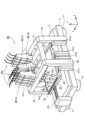
- FIG. 2 is a perspective view showing the outline of the external configuration of the main body of the exposure apparatus.
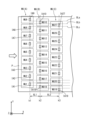
- FIG. 3 is a diagram showing an example of the arrangement of DMD projection areas projected onto a substrate by each projection unit of a plurality of exposure module groups.
- FIG. 4 is a diagram for explaining the state of continuous exposure by each of the four specific projection areas in FIG.
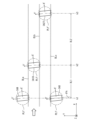
- FIG. 5 is an optical layout diagram showing a specific configuration of two exposure modules arranged in the X direction (scanning exposure direction) as viewed in the XZ plane.
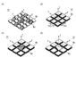
- FIG. 6(A) is a diagram showing a schematic diagram of a DMD, FIG.
- FIG. 6(B) is a diagram showing the DMD when the power is OFF
- FIG. 6(C) is a diagram for explaining the mirror in the ON state
- FIG. 6(D) is a diagram for explaining the mirror in the OFF state.
- FIG. 7 is a diagram showing an example of a data flow in the exposure apparatus according to the first embodiment.
- FIG. 8A is a diagram for explaining division of a plurality of micromirrors included in the DMD into segments
- FIG. 8B is a diagram for explaining SLM data generated by the module PC.
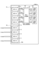
- FIG. 9 is a block diagram illustrating the configuration of the storage control board.
- FIG. 10 is a time chart showing the data transmission speed to the DMD control board, the read speed of the first memory, and the amount of data in the second storage unit.
- FIG. 11(A) is a diagram illustrating another example of a DMD segment
- FIG. 11(B) is a diagram illustrating SLM data stored in multiple first memories
- FIG. 11(C) is a diagram illustrating SLM data transferred from multiple first memories.
- FIG. 12 is a block diagram showing the configuration of a storage control board according to the second embodiment.
- FIG. 13(A) is a conceptual diagram showing the procedure when, after forming a pattern A on a substrate, a pattern B different from pattern A is formed on the substrate in an exposure apparatus according to the first embodiment
- FIG. 13(B) is a conceptual diagram showing the procedure when, after forming a pattern A on a substrate, a pattern B different from pattern A is formed on the substrate in an exposure apparatus according to the second embodiment.
- FIG. 13(A) is a conceptual diagram showing the procedure when, after forming a pattern A on a substrate, a pattern B different from pattern A is formed on the substrate in an exposure apparatus according to the second embodiment.
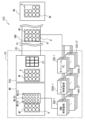
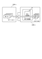
- FIG. 14 is a diagram showing an overview of an exposure system according to the third embodiment.
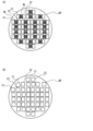
- 15A and 15B are diagrams for explaining a wiring pattern formed by an exposure system according to the third embodiment.
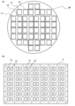
- FIG. 16A is a schematic diagram showing a wafer in which all chips are arranged in their designed positions
- FIG. 16B is a schematic diagram showing a wafer in which chips are arranged deviated from their designed positions.
- FIG. 17 is a conceptual diagram of a procedure for forming a wiring pattern in FO-WLP in the third embodiment.
- FIG. 18 is a diagram showing another example of the configuration of the module PC and the storage control board in the first to third embodiments.
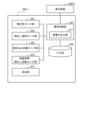
- FIG. 20 is a functional block diagram of an abnormality detection device according to the fourth embodiment.
- FIG. 21 is a functional block diagram of another example of the abnormality detection device.
- FIG. 22 is a flow chart showing a part of the manufacturing process when manufacturing a semiconductor device.
- FIG. 23 is a flow chart showing a part of the manufacturing process for manufacturing a liquid crystal display element.
- an XYZ Cartesian coordinate system is set, and the positional relationship of each component will be described with reference to this XYZ Cartesian coordinate system.
- a specific direction in a horizontal plane is defined as the X-axis direction
- a direction perpendicular to the X-axis direction in the horizontal plane is defined as the Y-axis direction
- a direction perpendicular to both the X-axis direction and the Y-axis direction i.e., the vertical direction
- the directions of rotation (tilt) around the X-axis, Y-axis, and Z-axis are defined as the ⁇ X, ⁇ Y, and ⁇ Z directions, respectively.
- FIG. 1 is a block diagram showing a schematic configuration of an exposure apparatus EX according to the first embodiment.
- the exposure apparatus EX includes a main body unit MB, a substrate exchange unit PCU, and a data transfer device 1000.
- FIG. 2 is a perspective view showing an outline of the external configuration of the main body MB of the exposure apparatus EX.
- the exposure apparatus EX is an apparatus that projects an exposure light, the intensity distribution of which in space is dynamically modulated by a spatial light modulator (SLM), onto an exposed substrate.
- the spatial light modulator include a liquid crystal element, a digital micromirror device (DMD), and a magneto-optic spatial light modulator (MOSLM).
- the exposure apparatus EX according to this embodiment includes a DMD 10 as a spatial light modulator, but may include other spatial light modulators.
- the exposure apparatus EX is a step-and-scan projection exposure apparatus (scanner) that exposes a rectangular (square) glass substrate used in display devices (flat panel displays) and the like.
- the glass substrate is a substrate P for flat panel displays, with at least one side or diagonal length of 500 mm or more and a thickness of 1 mm or less.
- the exposure apparatus EX exposes a projected image of a pattern created by the DMD 10 onto a photosensitive layer (photoresist) formed with a constant thickness on the surface of the substrate P.
- the substrate P which is removed from the exposure apparatus EX after exposure, is sent to a specified process step (film formation step, etching step, plating step, etc.) after the development step.
- the main body MB is equipped with a stage device consisting of a pedestal 2 placed on active vibration isolation units 1a, 1b, 1c, 1d (1d not shown), a base plate 3 placed on the pedestal 2, an XY stage 4A that can move two-dimensionally on the base plate 3, a substrate holder 4B that holds substrate P on a flat surface by suction on the XY stage 4A, and laser length measurement interferometers (hereinafter simply referred to as interferometers) IFX, IFY1 to IFY4 that measure the two-dimensional movement position of substrate holder 4B (substrate P).
- a stage device is disclosed, for example, in U.S. Patent Publication No. 2010/0018950 and U.S. Patent Publication No. 2012/0057140.
- the XY plane of the Cartesian coordinate system XYZ is set parallel to the flat surface of the base plate 3 of the stage device, and the XY stage 4A is set so as to be able to move in translation within the XY plane.
- the direction parallel to the X axis of the coordinate system XYZ is set as the scanning movement direction of the substrate P (XY stage 4A) during scanning exposure.
- the movement position of the substrate P in the X-axis direction is measured sequentially by the interferometer IFX, and the movement position in the Y-axis direction is measured sequentially by at least one (preferably two or more) of the four interferometers IFY1 to IFY4.
- the substrate holder 4B is configured to be able to move slightly in the Z-axis direction perpendicular to the XY plane relative to the XY stage 4A, and to be able to tilt slightly in any direction relative to the XY plane, and focus adjustment and leveling (parallelism) adjustment between the surface of the substrate P and the imaging plane of the projected pattern are actively performed. Furthermore, the substrate holder 4B is configured to be able to rotate slightly ( ⁇ z rotation) around an axis parallel to the Z axis in order to actively adjust the inclination of the substrate P in the XY plane.
- the main body MB further includes an optical base 5 that holds a plurality of exposure (drawing) module groups MU(A), MU(B), and MU(C), and main columns 6a, 6b, 6c, and 6d (6d not shown) that support the optical base 5 from the pedestal 2.
- Each of the plurality of exposure module groups MU(A), MU(B), and MU(C) is attached to the +Z side of the optical base 5.
- Each of the plurality of exposure module groups MU(A), MU(B), and MU(C) has an illumination unit ILU that is attached to the +Z side of the optical base 5 and that receives illumination light from the optical fiber unit FBU, and a projection unit PLU that is attached to the -Z side of the optical base 5 and has an optical axis parallel to the Z axis. Furthermore, each of the exposure module groups MU(A), MU(B), and MU(C) includes a DMD 10 that serves as a light modulation unit that reflects illumination light from the illumination unit ILU in the -Z direction and makes it incident on the projection unit PLU.
- the detailed configuration of the exposure module consisting of the illumination unit ILU, DMD 10, and projection unit PLU will be described later.
- the -Z direction side of the optical base 5 of the main body MB is fitted with a plurality of alignment systems (microscopes) ALG for detecting alignment marks formed at a plurality of predetermined positions on the substrate P.
- a calibration reference unit CU for calibration is provided at the end of the substrate holder 4B in the -X direction.
- Calibration includes at least one of the following: confirmation of the relative positional relationship in the XY plane of the detection field of each of the alignment systems ALG, confirmation of the baseline error between the projection positions of the pattern images projected from the projection units PLU of each of the exposure module groups MU(A), MU(B), and MU(C) and the position of the detection field of each of the alignment systems ALG, and confirmation of the position and image quality of the pattern images projected from the projection units PLU.
- each of the exposure module groups MU(A), MU(B), and MU(C) has nine modules arranged at regular intervals in the Y direction, but the number of modules may be less than or greater than nine.
- three rows of exposure modules are arranged in the X-axis direction, but the number of rows of exposure modules arranged in the X-axis direction may be two or less, or four or more.
- Figure 3 is a diagram showing an example arrangement of the projection areas IAn of the DMD 10 projected onto the substrate P by the projection units PLU of each of the exposure module groups MU(A), MU(B), and MU(C), with the Cartesian coordinate system XYZ set to the same as in Figure 2.
- the exposure module group MU(A) consists of nine modules MU1 to MU9 arranged in the +Y direction
- the exposure module group MU(B) consists of nine modules MU10 to MU18 arranged in the -Y direction
- the exposure module group MU(C) consists of nine modules MU19 to MU27 arranged in the +Y direction.
- Modules MU1 to MU27 all have the same configuration, and when exposure module group MU(A) and exposure module group MU(B) are arranged facing each other in the X direction, exposure module group MU(B) and exposure module group MU(C) are arranged back-to-back in the X direction.
- the shape of the projection areas IA1, IA2, IA3, ..., IA27 (sometimes referred to as IAn, where n is 1 to 27) by each of the modules MU1 to MU27 is, by way of example, a rectangle extending in the Y direction with an aspect ratio of approximately 1:2.
- patchwork exposure is performed at the -Y direction ends of each of the projection areas IA1 to IA9 in the first row and the +Y direction ends of each of the projection areas IA10 to IA18 in the second row.
- the areas on the substrate P that are not exposed by each of the projection areas IA1 to IA18 in the first and second rows are patchwork exposed by each of the projection areas IA19 to IA27 in the third row.
- the center point of each of the projection areas IA1 to IA9 in the first row is located on a line k1 parallel to the Y axis
- the center point of each of the projection areas IA10 to IA18 in the second row is located on a line k2 parallel to the Y axis
- the center point of each of the projection areas IA19 to IA27 in the third row is located on a line k3 parallel to the Y axis.
- the distance in the X direction between lines k1 and k2 is set to distance XL1
- the distance in the X direction between lines k2 and k3 is set to distance XL2.
- the orthogonal coordinate system XYZ is set to be the same as in Figures 2 and 3, and the coordinate system X'Y' in projection areas IA8, IA9, IA10, IA27 (and all other projection areas IAn) is set to be inclined at an angle ⁇ k with respect to the X and Y axes (lines k1 to k3) of the orthogonal coordinate system XYZ. That is, the entire DMD 10 is tilted by an angle ⁇ k in the XY plane so that the two-dimensional arrangement of the numerous micromirrors of the DMD 10 forms the coordinate system X'Y'.
- the circular area encompassing each of the projection areas IA8, IA9, IA10, IA27 (and all other projection areas IAn) in Figure 4 represents the circular image field PLf' of the projection unit PLU.
- the projected image of the micromirrors arranged diagonally (at an angle ⁇ k) at the -Y' end of projection area IA9 is set to overlap with the projected image of the micromirrors arranged diagonally (at an angle ⁇ k) at the +Y' end of projection area IA10.
- the projected image of the micromirrors arranged diagonally (at an angle ⁇ k) at the -Y' end of projection area IA10 is set to overlap with the projected image of the micromirrors arranged diagonally (at an angle ⁇ k) at the +Y' end of projection area IA27.
- the projected images of the micromirrors arranged diagonally (at an angle ⁇ k) at the end of the projection area IA8 in the +Y' direction and the projected images of the micromirrors arranged diagonally (at an angle ⁇ k) at the end of the projection area IA27 in the -Y' direction are set to overlap.
- [Configuration of lighting unit] 5 is an optical layout diagram showing the specific configuration of the module MU18 in the exposure module group MU(B) shown in FIG. 2 and the module MU19 in the exposure module group MU(C) shown in FIG. 3, viewed in the XZ plane.
- the orthogonal coordinate system XYZ in FIG. 5 is set to be the same as the orthogonal coordinate system XYZ in FIG. 2 to FIG. 4.
- the module MU18 is shifted by a certain distance in the +Y direction with respect to the module MU19, and is installed back-to-back.
- the optical fiber unit FBU shown in FIG. 2 is composed of 27 optical fiber bundles FB1 to FB27 corresponding to each of the 27 modules MU1 to MU27 shown in FIG. 3.
- the illumination unit ILU of the module MU18 is composed of a mirror 100 that reflects the illumination light ILm traveling in the -Z direction from the output end of the optical fiber bundle FB18, a mirror 102 that reflects the illumination light ILm from the mirror 100 in the -Z direction, an input lens system 104 that acts as a collimator lens, an illuminance adjustment filter 106, an optical integrator 108 that includes a micro fly's eye (MFE) lens and a field lens, a condenser lens system 110, and an inclined mirror 112 that reflects the illumination light ILm from the condenser lens system 110 toward the DMD 10.
- the mirror 102, the input lens system 104, the optical integrator 108, the condenser lens system 110, and the inclined mirror 112 are arranged along an optical axis AXc that is parallel to the Z axis.
- the optical fiber bundle FB18 is composed of one optical fiber line or a bundle of multiple optical fiber lines.
- the illumination light ILm irradiated from the output end of the optical fiber bundle FB18 (each of the optical fiber lines) is set to a numerical aperture (NA, also called a spread angle) such that it is incident without being eclipsed by the input lens system 104 in the subsequent stage.
- NA numerical aperture
- the position of the front focal point of the input lens system 104 is designed to be the same as the position of the output end of the optical fiber bundle FB18.
- the position of the back focal point of the input lens system 104 is set so that the illumination light ILm from a single or multiple point light sources formed at the output end of the optical fiber bundle FB18 is superimposed on the incident surface side of the MFE lens 108A of the optical integrator 108. Therefore, the incident surface of the MFE lens 108A is Koehler illuminated by the illumination light ILm from the output end of the optical fiber bundle FB18.
- the geometric center point in the XY plane of the output end of the optical fiber bundle FB18 is located on the optical axis AXc, and the chief ray (center line) of the illumination light ILm from the point light source at the output end of the optical fiber line is parallel (or coaxial) with the optical axis AXc.
- the illumination light ILm from the input lens system 104 is attenuated by an arbitrary value in the range of 0% to 90% by the illuminance adjustment filter 106, and then passes through the optical integrator 108 (MFE lens 108A, field lens, etc.) and enters the condenser lens system 110.
- the MFE lens 108A is a two-dimensional array of many rectangular microlenses with a side length of several tens of ⁇ m, and its overall shape is set to be approximately similar to the overall shape of the mirror surface of the DMD 10 (aspect ratio is approximately 1:2) in the XY plane.
- the position of the front focal point of the condenser lens system 110 is set to be approximately the same as the position of the exit surface of the MFE lens 108A. Therefore, each of the illumination lights from the point light sources formed on the exit side of each of the many microlenses of the MFE lens 108A is converted into an approximately parallel light beam by the condenser lens system 110, reflected by the inclined mirror 112, and then superimposed on the DMD 10 to form a uniform illuminance distribution.
- the exit surface of the MFE lens 108A generates a surface light source in which many point light sources (light focusing points) are densely arranged in a two-dimensional manner, so it functions as a surface light source component.
- the optical axis AXc which is parallel to the Z axis and passes through the condenser lens system 110, is bent by the tilted mirror 112 to reach the DMD 10, and the optical axis between the tilted mirror 112 and the DMD 10 is the optical axis AXb.
- the neutral plane including the center points of each of the many micromirrors of the DMD 10 is set parallel to the XY plane. Therefore, the angle between the normal to the neutral plane (parallel to the Z axis) and the optical axis AXb is the incident angle ⁇ of the illumination light ILm to the DMD 10.
- the DMD 10 is attached to the underside of the mount 10M fixed to the support column of the illumination unit ILU.
- the mount 10M is provided with a fine movement stage that combines a parallel link mechanism and an expandable piezoelectric element, for example, as disclosed in International Patent Publication No. 2006/120927.
- Fig. 6(A) is a diagram showing a schematic of the DMD 10
- Fig. 6(B) is a diagram showing the DMD 10 when the power is OFF
- Fig. 6(C) is a diagram for explaining the mirror in the ON state
- Fig. 6(D) is a diagram for explaining the mirror in the OFF state. Note that in Figs. 6(A) to 6(D), mirrors in the ON state are shown by hatching.
- the DMD 10 has multiple micromirrors Ms whose reflection angles can be changed and controlled.
- the DMD 10 uses a roll and pitch drive system that switches between the ON and OFF states by tilting the micromirrors Ms in the roll and pitch directions.
- each micromirror Ms when the power is off, the reflecting surface of each micromirror Ms is set parallel to the X'Y' plane.
- Each micromirror Ms is turned ON by tilting around the Y' axis.
- FIG. 6C shows a case where only the central micromirror Ms is turned ON, and the other micromirrors Ms are in a neutral state (neither ON nor OFF).
- Each micromirror Ms is turned OFF by tilting around the X' axis.
- FIG. 6D shows a case where only the central micromirror Ms is turned OFF, and the other micromirrors Ms are in a neutral state.
- the micromirror Ms in the ON state is driven to tilt at a predetermined angle from the X'Y' plane so that the illumination light irradiated to the micromirror Ms in the ON state is reflected in the X direction of the XZ plane.
- the micromirror Ms in the OFF state is driven to tilt at a predetermined angle from the X'Y' plane so that the illumination light irradiated to the micromirror Ms in the ON state is reflected in the Y direction in the YZ plane.
- the DMD 10 generates an exposure pattern by switching the ON and OFF states of each micromirror Ms.
- the illumination light reflected by the mirror in the OFF state is absorbed by a light absorber (not shown).
- the DMD 10 has been described as an example of a spatial light modulation element, and therefore as a reflective type that reflects laser light, but the spatial light modulation element may be a transmissive type that transmits laser light, or a diffractive type that diffracts laser light.
- the spatial light modulation element can modulate the laser light spatially and temporally.
- illumination light ILm irradiated to one of the micromirrors Ms of the DMD 10 that is in the ON state is reflected in the X direction in the XZ plane so as to head toward the projection unit PLU.
- illumination light ILm irradiated to one of the micromirrors Ms of the DMD 10 that is in the OFF state is reflected in the Y direction in the YZ plane so as not to head toward the projection unit PLU.
- a movable shutter 114 is removably provided in the optical path between the DMD 10 and the projection unit PLU to block reflected light from the DMD 10 during non-exposure periods. As shown on the module MU19 side, the movable shutter 114 is rotated to an angular position where it is removed from the optical path during exposure periods, and is rotated to an angular position where it is inserted obliquely into the optical path during non-exposure periods, as shown on the module MU18 side. A reflective surface is formed on the DMD 10 side of the movable shutter 114, and the light from the DMD 10 reflected there is irradiated onto the light absorber 117.
- the light absorber 117 absorbs light energy in the ultraviolet wavelength range (wavelengths of 400 nm or less) without re-reflecting it and converts it into heat energy. For this reason, the light absorber 117 is also provided with a heat dissipation mechanism (heat dissipation fins and a cooling mechanism). Although not shown in FIG. 5, the reflected light from the micromirror Ms of the DMD 10, which is in the OFF state during the exposure period, is absorbed by a similar light absorber (not shown in FIG. 5) installed in the Y direction (a direction perpendicular to the paper surface of FIG. 5) with respect to the optical path between the DMD 10 and the projection unit PLU, as described above.
- a similar light absorber not shown in FIG. 5 installed in the Y direction (a direction perpendicular to the paper surface of FIG. 5) with respect to the optical path between the DMD 10 and the projection unit PLU, as described above.
- the projection unit PLU attached to the underside of the optical base 5 is configured as a double-telecentric imaging projection lens system composed of a first lens group 116 and a second lens group 118 arranged along an optical axis AXa parallel to the Z axis.
- the first lens group 116 and the second lens group 118 are configured to translate in a direction along the Z axis (optical axis AXa) by a micro-movement actuator, respectively, relative to a support column fixed to the underside of the optical base 5.
- the projection magnification Mp is set to approximately 1/6, taking into consideration the tilt angle ⁇ k in the XY plane of the projection area IAn (DMD10) described above in FIG. 4.
- the imaging projection lens system consisting of lens groups 116 and 118 inverts/flips a reduced image of the entire mirror surface of DMD10 and images it on the projection area IA18 (IAn) on the substrate P.
- the first lens group 116 of the projection unit PLU can be moved slightly in the direction of the optical axis AXa by an actuator to fine-tune the projection magnification Mp (approximately ⁇ several tens of ppm), and the second lens group 118 can be moved slightly in the direction of the optical axis AXa by an actuator to quickly adjust the focus. Furthermore, in order to measure the positional change in the Z-axis direction of the surface of the substrate P with an accuracy of submicron or less, multiple focus sensors 120 of the oblique incidence type are provided below the optical table 5.
- the illumination unit ILU and projection unit PLU described above require the projection area IAn to be tilted by an angle ⁇ k in the XY plane, so the DMD 10 and illumination unit ILU in Figure 5 (at least the optical path portion from mirror 102 to inclined mirror 112 along the optical axis AXc) are positioned so that they are tilted overall by an angle ⁇ k in the XY plane.
- the substrate replacement unit PCU is equipped with a port PT, and transports the substrate P that has been exposed in the main body unit MB from the main body unit MB described above, and transports the substrate P to be next exposed (unprocessed substrate P) into the main body unit MB.
- the data transfer device 1000 includes modular PCs (Personal Computers) 200-1 to 200-27, storage control boards 300-1 to 300-27, and DMD control boards 400-1 to 400-27.
- modular PCs Personal Computers
- Module PC200-1 to 200-27, storage control boards 300-1 to 300-27, and DMD control boards 400-1 to 400-27 are provided to correspond to modules MU1 to MU27, respectively.
- FIG. 7 is a diagram showing an example of data flow in the exposure apparatus EX according to the first embodiment.
- CAD Computer Aided Design
- the mask data server MDS converts the input CAD data into a bitmap (BMP) file. Since the capacity of this BMP file is enormous, for example several tens of TB, the mask data server MDS creates compressed mask data (drawing data) (first data) by compressing the BMP file.
- BMP bitmap
- Module PC200-n downloads compressed mask data created by the mask data server MDS.
- Module PC200-n divides the downloaded compressed mask data to generate SLM data indicating the exposure pattern to be generated by the DMD10 of the corresponding module MUn.
- the SLM data may be calculated at high speed using a dedicated board such as a GPU or FPGA, in addition to the module PC200-n.
- the SLM data may also be calculated by a third processing unit 61 provided on the storage control board 300-n, which will be described later.
- the functions of the module PC may be included in the storage control board.
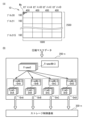
- Figure 8(A) is a diagram for explaining the division of the micromirror Ms of the DMD 10 into segments in this embodiment
- Figure 8(B) is a diagram for explaining the SLM data generated by module PC200-n.
- the DMD 10 has 2560 x 1600 micromirrors Ms.
- the module PC 200-n divides the 2560 x 1600 micromirrors Ms into 4 segments (segments A to D) x 16 blocks (blocks 0 to 15). Note that the number of micromirrors Ms, the number of segments, and the number of blocks provided in the DMD 10 are not limited to those in this embodiment.
- the module PC200-n generates SLM data DnA to DnD corresponding to the multiple segments A to D of the DMD10, respectively, and writes them to the storage control board 300-n.
- module PC200-n creates SLM data Frame1 indicating the exposure pattern to be generated by DMD10 of module MUn at a second timing, and creates divided data Frm1-DnA to Frm1-DnD by dividing SLM data Frame1 to correspond to segments A to D.
- module PC200-n creates SLM data up to SLM data Frame4N+3 (N is a natural number)
- divided data Frm4N+3-DnA to Frm4N+3-DnD are created from divided data Frm0-DnA to Frm0-DnD.
- the module PC200-n transfers the divided data for each segment that it has created to the storage control board 300-n as SLM data DnA to DnD.
- the second storage unit 60 is mounted on a third processing unit 61.
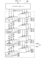
- the second storage unit 60 reads out the SLM data DnA to DnD from the first memories 50-1 to 50-4, temporarily stores them, and transmits (transfers) the temporarily stored SLM data DnA to DnD to the DMD control board 400-n.
- the module M Un selectively drives the micromirrors Ms of the DMD 10 based on the received data DMn to generate exposure patterns corresponding to the data DMn, and projects and exposes them onto the substrate P.
- the first memories 50-1 to 50-4 provided in the storage control board 300-n operate in parallel. That is, the first memories 50-1 to 50-4 can transfer the SLM data DnA to DnD to the second storage unit 60 independently without being affected by the other first memories.
- the transfer time of the SLM data (for example, SLM data Frame 0) can be shortened even when using the first memories.
- four first memories 50-1 to 50-4 are provided, so for example, SLM data Frame 0 can be transferred in about 1/4 the time it takes to transfer SLM data Frame 0 from one first memory.
- the transfer speed of the second storage unit 60 is slower than the transfer speed of the first memories 50-1 to 50-4.
- This embodiment is also effective when the transfer speed of the second storage unit 60 is faster than the transfer speed of the first memories 50-1 to 50-4.
- the number of transmit terminals TX1 to TX4 and receive terminals RX1 to RX4 is the same as the number of segments, but the number of transmit terminals TX1 to TX4 and receive terminals RX1 to RX4 is not limited to this.
- the second storage unit 60 is provided so that even if the read speed of the first memory 50-m varies and decreases, the transfer of SLM data is not affected. In other words, the second storage unit 60 functions as a buffer.
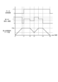
- time t1 is the exposure start time
- time t5 is the exposure end time.
- a predetermined amount of SLM data (FULL) is stored in the second storage unit 60.
- the SLM data in the second storage unit 60 is read out and transmitted to the DMD control board 400-n.
- the transmission speed at this time is r11.
- the read speed r11 of the first memory 50-m is the same as the transmission speed r11, so the amount of data in the second storage unit 60 remains FULL.
- the read speed of the first memory 50-m becomes r1, which is slower than the transmission speed r11, the amount of data transmitted from the second storage unit 60 is greater than the amount of data read from the first memory 50-m to the second storage unit 60, so the amount of data in the second storage unit 60 decreases.
- the data in the second storage unit 60 is not depleted, no SLM data is lost and no exposure failure occurs.
- the minimum required capacity of the second storage unit 60 will be explained.
- the capacity of the second storage unit 60 will be described as the buffer capacity, which is the amount of data that can be exposed without data loss while the exposure device is exposing, taking into account whether or not there is a decrease in the speed of the first memory.
- Minimum required buffer capacity ⁇ (data transfer rate to DMD control board ⁇ transfer rate when read rate of first memory is reduced) ⁇ time during which read rate of first memory is reduced ⁇ (1)
- Minimum required buffer capacity ⁇ data transfer rate to DMD control board ⁇ nominal value of readout rate of first memory ⁇ scanning time ⁇ + ⁇ (data transfer rate to DMD control board ⁇ transfer rate when readout rate of first memory is reduced) ⁇ time during which readout rate of first memory is reduced ⁇ (2)
- the "transfer speed when the read speed of the first memory slows down” may be replaced with the "transfer speed assuming a slowdown in the read speed of the first memory”
- the "time during which the read speed of the first memory slows down” may be replaced with the "assumed time for which the read speed of the first memory slows down”.
- the minimum required buffer capacity is determined appropriately based on the specifications of the exposure apparatus EX and the specifications of the first memory installed.
- the storage control board 300-n has a plurality of first memories 50-1 to 50-4 that store the SLM data DnA to DnD transferred from the module PC 200-n, and transfers the SLM data DnA to DnD from each of the plurality of first memories 50-1 to 50-4, and a second storage unit 60 that stores the SLM data DnA to DnD transferred from the plurality of first memories 50-1 to 50-4 and transfers the SLM data DnA to DnD to the DMD 10.
- the module PC200-n divides the multiple micromirrors Ms into multiple segments A to D to generate the SLM data DnA to DnD, and generates the SLM data DnA to DnD corresponding to each of the multiple segments A to D from the compressed mask data. This allows the SLM data DnA to DnD to be transferred from the first memories 50-1 to 50-4, which operate in parallel, respectively, thereby shortening the transfer time of the SLM data.
- the first memories 50-1 to 50-4 are provided corresponding to the multiple segments of the DMD 10, but the method of dividing the DMD 10 into segments is not limited to that shown in FIG. 8(A).
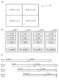
- the DMD 10 may be divided into four segments as shown in FIG. 11(A).
- the number of segments into which the DMD 10 is divided is not limited to four, and may be two or three, or five or more.
- the SLM data Frame0 indicating the exposure pattern to be generated by the multiple micromirrors Ms at the first control timing is divided to correspond to the segments A to D into which the micromirrors Ms of the DMD 10 are divided, and the divided data Frm0-DnA to Frm0-DnD are stored in the first memories 50-1 to 50-4, respectively, but this is not limited to the above.
- SLM data Frame 0 indicating the exposure pattern to be generated by the multiple micromirrors Ms of the DMD 10 at the first control timing may be stored, for example, in the first memory 50-1 without being divided
- SLM data Frame 1 indicating the exposure pattern to be generated by the multiple micromirrors Ms of the DMD 10 at the second control timing may be stored, for example, in the first memory 50-2 without being divided.
- the first memory 50-1 may store SLM data Frame 0, Frame 4, Frame 8, ..., Frame 4N (N is a natural number), the first memory 50-2 may store SLM data Frame 1, Frame 5, Frame 9, ..., Frame 4N+1, the first memory 50-3 may store SLM data Frame 2, Frame 6, Frame 10, ..., Frame 4N+2, and the first memory 50-4 may store SLM data Frame 3, Frame 7, Frame 11, ..., Frame 4N+3.
- FIG. 11C is a diagram that shows an outline of the reading of SLM data from the first memories 50-1 to 50-4.
- the SLM data Frame 0 of the first control timing is read from the first memory 50-1.
- reading of the SLM data Frame 1 from the first memory 50-2 starts.
- reading of the SLM data Frame 2 from the first memory 50-3 starts, and when 1/4 of the data of the SLM data Frame 2 has been read, reading of the SLM data Frame 3 from the first memory 50-4 starts.
- the SLM data indicating the exposure pattern to be generated by the micromirrors Ms of the DMD 10 may be transmitted in a time-division manner. Even with this configuration, it is possible to reduce the transfer time of the SLM data corresponding to the entire pattern formed on the substrate P in one scan (exposure process) compared to the case where there is one first memory. Note that when the SLM data is transmitted in a time-division manner, the SLM data is merged in the second storage unit 60.
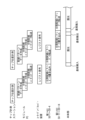
- a second embodiment Next, a second embodiment will be described.
- Fig. 12 is a block diagram showing the configuration of the storage control board 300A-n according to the second embodiment.
- the first storage unit 50A provided in the storage control board 300A-n according to the second embodiment includes a first memory group G1 including first memories 50-1 to 50-4, and a second memory group G2 including first memories 50-11 to 50-14.
- the second storage unit 60 is capable of switching its connection between the first memory group G1 and the second memory group G2.
- the SLM data A-DnA to A-DnD for forming pattern A on substrate P stored in the first memories 50-1 to 50-4 of the first memory group G1 is read into the second storage unit 60, and while the exposure process is being performed, the SLM data B-DnA to B-DnD for forming pattern B (next lot) different from pattern A is written into the first memories 50-11 to 50-14 of the second memory group G2.
- the reading of the SLM data A-DnA to A-DnD from the first memories 50-1 to 50-4 of the first memory group G1 and the writing of the SLM data B-DnA to B-DnD into the first memories 50-11 to 50-14 of the second memory group G2 are performed in parallel.
- the SLM data is written to the first memories 50-11 to 50-14 of the second memory group G2 during the exposure process, but the SLM data may be written during substrate alignment or during calibration of the exposure apparatus. Also, in the first embodiment, the SLM data may be transferred to the first memories 50-1 to 50-4 during substrate alignment or during calibration of the exposure apparatus.
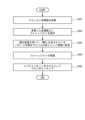
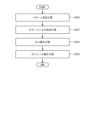
- Figure 13(A) is a conceptual diagram showing the procedure for forming pattern A on a substrate and then forming pattern B, which is different from pattern A, on the substrate in the exposure apparatus EX according to the first embodiment.
- the first memories 50-1 to 50-4 are used to transfer the SLM data from the first memories 50-1 to 50-4 to the second storage unit 60, so the SLM data of pattern B cannot be written to the first memories 50-1 to 50-4.
- the process of writing the SLM data of pattern B to the first memories 50-1 to 50-4 becomes possible, so as shown in FIG. 13A, for example, the process of writing the SLM data of pattern B to the first memories 50-1 to 50-4 is started after the exposure process of pattern A. Note that the process of writing the SLM data of pattern B to the first memories 50-1 to 50-4 may be started immediately after the transfer of the SLM data of pattern A is completed.
- the second storage unit 60 is connected to the first memories 50-1 to 50-4 of the first memory group G1.
- the writing of the SLM data of pattern B to the first memories 50-11 to 50-14 of the second memory group G2 is executed in parallel with the transfer of SLM data to the second storage unit 60 and the exposure process of pattern A.
- the connection of the second storage unit 60 is changed to the first memories 50-11 to 50-14 of the second memory group G2
- the SLM data is read from the first memories 50-11 to 50-14 to the second storage unit 60, and the exposure process of pattern B is performed.
- the exposure process and the process of writing SLM data to the first memories can be performed in parallel, thereby improving the throughput of the exposure apparatus EX as a whole.
- the storage control board 300A-n has a first memory group G1 including a plurality of first memories 50-1 to 50-4 that store the SLM data transferred from the module PC200-n, and a second memory group G2 including a plurality of first memories 50-11 to 50-14 that are different from the first memory group G1. While the SLM data A-DnA to A-DnD of pattern A stored in the plurality of first memories 50-1 to 50-4 of the first memory group G1 is being transferred to the second storage unit 60, the module PC200-n writes the SLM data B-DnA to B-DnD of pattern B, which is different from pattern A, to the first memories 50-11 to 50-14 of the second memory group G2. This allows the time-consuming process of writing the SLM data to the first memory to be performed behind the scenes of the exposure process, thereby improving the throughput of the exposure apparatus EX.
- the third embodiment describes the case where a rewiring layer that connects pads of a semiconductor chip is formed using an exposure apparatus EX in the manufacture of semiconductor device packages called FO-WLP (Fan Out Wafer Level Package) and FO-PLP (Fan Out Plate Level Package).
- FO-WLP Full Wafer Level Package
- FO-PLP Full Plate Level Package
- FIG. 14 is a diagram showing an overview of an exposure system EXS according to the third embodiment.
- the exposure system EXS is a system for forming wiring patterns that connect between semiconductor chips (hereinafter referred to as chips) arranged on a wafer WF, as shown in FIG. 15(A), or between chips arranged on a substrate P, as shown in FIG. 15(B).
- a wiring pattern is formed that connects between chips C1 and C2 included in each set (indicated by a two-dot chain line) of chips arranged on a wafer WF or a substrate P.
- the number of chips included in each set is two, but this is not limited to this and may be three or more.
- the exposure system EXS includes a wafer placement device WA, a chip measurement station CMS, a coater developer device CD, and an exposure device EX.
- the exposure device EX includes the storage control board 300A-n according to the second embodiment.
- the wafer placement device WA attaches multiple wafers WF, on which chips are placed, to a base substrate B.
- the chip measurement station CMS is equipped with multiple measurement microscopes 81 and measures the positions of chips in different sets.
- the positions of chips in different sets measured by the multiple measurement microscopes 81 may be the positions of chips in different sets on the same wafer WF, or the positions of chips in each set on different wafers WF.
- the multiple measurement microscopes 81 measure the positions of chips in each set on different wafers WF.
- FIG. 16(A) is a schematic diagram showing the wafer WF in a state where all chips are arranged in the design positions (hereinafter referred to as the design positions).
- the wiring pattern WL connecting the chips C1 and C2 is exposed (formed) by the exposure apparatus EX.
- FO-WLP the chips are solidified on the wafer WF with a molding material such as resin, so that the position of each chip may deviate from the design position, as shown in FIG. 16(B).
- the DMD 10 is controlled to expose the wiring pattern using SLM data (hereinafter referred to as the design value data) showing the wiring pattern connecting the chips at the design positions, the wiring pattern may deviate from the pad position, resulting in poor connection or short circuit.
- SLM data hereinafter referred to as the design value data
- wiring pattern data is created by correcting part of the design value data based on the measurement results of the positions of the chips included in each set of multiple chips arranged on the wafer WF.
- the module PC200-n creates wiring pattern data based on the measurement results of the chip position received from the chip measurement station CMS.
- the wiring pattern data created by the module PC200-n is stored in a memory group different from the memory group in which the wiring pattern data used for exposure control of the substrate currently being exposed is stored. In other words, if the wiring pattern data used for exposure control of the wafer WF currently being exposed is stored in the first memories 50-1 to 50-4 of the first memory group G1, the module PC200-n stores (transfers) the created wiring pattern data in the first memories 50-11 to 50-14 of the second memory group G2.
- the wafer WF is carried into the coater developer device CD together with the base substrate B, where it is coated with a photosensitive resist and then carried into the port PT of the substrate exchange unit PCU.
- the wafer WF together with the base substrate B is then placed on the substrate holder 4B of the XY stage 4A.
- Figure 17 is a conceptual diagram of the wiring pattern formation procedure for FO-WLP in the third embodiment.
- the module PC 200-n when the chip position is measured in the chip measurement station CMS, the module PC 200-n creates wiring pattern data based on the measurement results of the chip position, and creates divided wiring pattern data by dividing the created wiring pattern data into segments.
- the module PC 200-n transfers the divided wiring pattern data to the first memories 50-1 to 50-4.
- the divided wiring pattern data is written to the first memories 50-1 to 50-4.
- the divided wiring pattern data stored in the first memories 50-1 to 50-4 is transferred sequentially to the DMD control board 400-n in synchronization with the start of exposure of the wafer WF.
- the chip measurement station CMS starts measuring the chip position of the wafer WF that will be next exposed by the main body MB.
- the module PC200-n creates wiring pattern data based on the chip position measurement results, and creates divided wiring pattern data by dividing the created wiring pattern data into segments.
- the module PC200-n transfers the divided wiring pattern data to the first memories 50-11 to 50-14.
- the divided wiring pattern data stored in the first memories 50-11 to 50-14 are transferred sequentially to the DMD control board 400-n in accordance with the start of exposure of the wafer WF on the board holder 4B.
- the time required for measuring the chip position and for creating and transferring wiring pattern data can be hidden in the time required for exposure processing. This improves the throughput in forming wiring patterns in FO-WLP.
- This type of parallel processing is particularly effective when it takes a long time to create, transfer, and store wiring pattern data.
- the multiple first memories in the first storage unit 50 or 50A may be SSDs (Solid State Drives), DRAMs (Dynamic Random Access Memory), flash memory, HDDs (Hard Disk Drives), MRAMs (Magnetic Random Access Memory), RAID storage, or network storage.
- the second storage unit 60 may be HBMs (High Bandwidth Memory), DRAMs (Dynamic Random Access Memory), or SRAMs (Static Random Access Memory).
- this embodiment is not limited to FO-WLP and FO-PLP, but can also be used when manufacturing semiconductor chips and flat panel displays.
- Semiconductor chips and flat panel displays are manufactured by overlaying several to several tens of different patterns on the chip C1, so accurate overlay exposure on the chip C1 is required. Therefore, when the chip position is measured on the chip measurement station CMS, the module PC200-n creates wiring pattern data based on the measurement results of the chip position, and creates divided wiring pattern data by dividing the created wiring pattern data into segments. This enables the module MUn to expose at the correct position.
- the first memories 50-1 to 50-4 may be provided in the module PC 200B-n instead of the storage control board 300B-n, as shown in FIG. 18.
- TBW Total Bytes Written
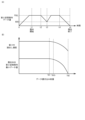
- Figure 19 (A) is a time chart showing the change in the amount of data in the second memory unit 60 during exposure processing
- Figure 19 (B) is a diagram showing the first memory read speed relative to the total amount of data written, and the minimum amount of data in the second memory unit 60 during exposure.
- the amount of data in the second memory unit 60 remains FULL. Then, for example, at time t2, if the read speed of the first memory decreases or the reading of data from the first memory is temporarily stopped and the amount of data transferred from the first memory to the second memory unit 60 falls below the amount of data transferred from the second memory unit 60, the amount of data in the second memory unit 60 decreases. Then, at time t3, when the read speed of the first memory again exceeds the data transfer speed from the second memory unit 60, the amount of data in the second memory unit 60 increases.
- the minimum data amount is defined as the minimum value MIN of the amount of data in the second memory unit 60 during the period from when exposure begins until all of the SLM data in the first memory is transferred to the second memory unit 60 (the period from time t1 to time t4).
- the read speed of the first memory remains almost constant while the total amount of data written is less than the first amount TA1, and begins to gradually decrease when it exceeds the first amount TA1.
- the minimum data amount in the second memory unit 60 remains almost constant until the total amount of data written becomes the first amount TA1, but when it exceeds the first amount TA1, it gradually decreases, and when it reaches the second amount TA2, the minimum data amount becomes 0.
- the minimum data amount becomes 0 the data in the second memory unit 60 is depleted, resulting in poor exposure. Therefore, it is desirable to replace the first memory when the total amount of data written is less than the second amount TA2.
- the total amount of data written and the minimum amount of data in the second storage unit 60 during exposure processing are obtained, and the total amount of data written at which the data in the second storage unit 60 is depleted (second amount TA2) is obtained.
- the total amount of data written TAth that is, for example, a predetermined percentage (for example, 20% to 30%) lower than the second amount TA2 is set as the special TBW. Therefore, a special TBW is set as the lifespan for each of the first memories 50-m used in the exposure apparatus EX according to this embodiment. Theoretically, the value of the special TBW is equal to or greater than the value of TBW.
- the abnormality detection device is provided, for example, in the data transfer device 1000.
- CRC Cyclic Redundancy Check
- it checks the consistency of the data by comparing the CRC code recalculated from the read SLM data with the read CRC code.
- the consistency monitor unit 601 stores the SLM data together with the CRC code calculated from the SLM data.
- the consistency monitor unit 601 compares the data before being stored in the storage control board 300-n with the data (1) to (3) to monitor the presence or absence of different signals.
- the consistency monitor unit 601 outputs the calculated bit error rate to the abnormality determination unit 607.
- the abnormality determination unit 607 stores in the log DB 609 the timing at which the bit error rate becomes equal to or greater than the threshold value BERth.
- the abnormality determination unit 607 may output an alert when the bit error rate becomes equal to or greater than the preset threshold value BERth.
- the threshold value BERth is set to a value that can maintain the desired exposure quality.
- the abnormality determination unit 607 stores in the log DB 609 the timing at which the minimum data amount became equal to or less than the threshold MDAth.
- the abnormality determination unit 607 may output an alert when the minimum data amount is equal to or less than the preset threshold MDAth.
- the abnormality determination unit 607 stores in the log DB 609 the timing at which the total amount of data written exceeded the special TBW.
- the abnormality determination unit 607 may output an alert when the total amount of data written exceeds the special TBW.
- the alert may be output, for example, by outputting a message to a display device DSPLY such as a liquid crystal display equipped in the exposure apparatus EX, or by displaying or printing out part of the data stored in the log DB 609 on the display device DSPLY.
- the alert may be output each time the processing of one substrate is completed, or may be output for each lot. When output for each lot, it may be configured to output that a substrate has occurred on which an error has occurred.
- a predetermined period e.g., the processing period of one lot
- a value equal to or greater than the TBW (special TBW) is set as the lifespan for each of the multiple first memories 50-m. Because the special TBW is greater than the TBW, the replacement interval for the first memory 50-m can be made longer compared to when the first memory 50-m is replaced based on the TBW. Therefore, the lifetime cost of the exposure apparatus EX can be reduced.
- the abnormality detection device 600-n includes a consistency monitor unit 601 that compares the SLM data before it is stored in the storage control board 300-n with the SLM data transferred from the storage control board 300-n to calculate the bit error rate (monitors the presence or absence of different signals). This makes it possible to check whether data consistency is maintained.
- the consistency monitor unit 601 compares the SLM data before it is stored in the storage control board 300-n with the SLM data transferred from the second storage unit 60 to calculate the bit error rate (monitors the presence or absence of different signals). This makes it possible to check whether the consistency of the data is maintained.
- the abnormality detection device 600-n includes an abnormality determination unit 607 that displays a warning (alert) on the display device DSPLY when the bit error rate measured by the consistency monitor unit 601 is equal to or greater than the threshold value BERth. This allows the operator of the exposure apparatus EX to know when to replace the first memory 50-m.
- the special TBW is determined based on the minimum amount of data in the second storage unit 60, but this is not limited to the above. If there is a correlation between the total amount of written data and the bit error rate, the special TBW may be determined based on the bit error rate. For example, if there is a relationship in which the bit error rate increases when the total amount of written data exceeds the first amount TA1, the total amount of written data at which the bit error rate exceeds a threshold value may be set as the special TBW. In addition, the special TBW may be determined using both the minimum amount of data in the second storage unit 60 and the bit error rate.
- the anomaly detection device 600-n only needs to have at least two of the consistency monitor unit 601, the read speed monitor unit 603, and the total write amount monitor unit 605.
- the temperature near the second storage unit 60 and the temperature near the first memory may be measured. At least one of an operational guarantee temperature and a performance guarantee temperature is provided for each component by the manufacturer. For example, if the first memory or the second storage unit 60 is used at a temperature outside the operational guarantee temperature, there is a risk that it will not operate normally. Therefore, an error (alert) may be output when the temperature near the second storage unit 60 and the temperature near the first memory are outside their respective operational guarantee temperatures.
- the SLM data DnA is stored in two or more different addresses (first address, second address) in the first memory 50-1. If the data transfer speed of the SLM data DnA from the first address of the first memory 50-1 to the second storage unit 60 is slow for some reason, the transfer source is changed from the first address to the second address during data transfer, and the SLM data DnA is transferred to the second storage unit 60. This makes it possible to prevent a delay in the data transfer speed. In addition, when changing the transfer source from the first address to the second address, it is preferable that the data transferred from the second address be transferred from the continuation of the SLM data transferred from the first address.
- the exposure position (imaging position) is corrected in each module MU1 to 27, so there is no need to modify the SLM data to adjust the exposure position.
- the exposure position can be adjusted by adjusting the position of the lens in each module MU1 to 27. Therefore, the same SLM data can be used continuously even for different substrates and different scan (product) areas. This eliminates the need for a data transfer process for each substrate, which shortens the data transfer time and increases the device operation time.
- exposure data is transferred for each substrate, data transfer must be performed even during exposure, and the DMD cannot be operated at high speed. This is because the data transfer may not be able to keep up with the high speed operation of the DMD, resulting in the risk of exposure not being possible.
- the above first to fourth embodiments can be applied to exposure apparatuses used in the manufacture of liquid crystal display elements, exposure apparatuses used in the manufacture of displays including semiconductor elements and the like to transfer device patterns onto semiconductor substrates, exposure apparatuses used in the manufacture of thin-film magnetic heads to transfer device patterns onto ceramic wafers, and exposure apparatuses used in the manufacture of imaging elements such as CCDs.
- FIG. 22 is a flow chart showing part of the manufacturing process when manufacturing a semiconductor device as a microdevice.
- a metal film is evaporated onto one lot of wafers.
- a photoresist is applied onto the metal film on the one lot of wafers.
- step S503 using the exposure apparatus EX shown in FIG. 1, an image of the pattern generated by the DMD 10 is sequentially exposed and transferred onto each shot area on the one lot of wafers via its projection optical system (projection system).
- step S504 the photoresist on that one lot of wafers is developed (developing process), and then in step S505, etching is performed on that one lot of wafers using the resist pattern as a mask, thereby forming a circuit pattern corresponding to the pattern generated by the DMD 10 in each shot area on each wafer. Then, by forming a circuit pattern on an upper layer, devices such as semiconductor elements are manufactured. According to the semiconductor device manufacturing method described above, semiconductor devices having extremely fine circuit patterns can be obtained with good throughput.
- a so-called photolithography process is carried out in which the pattern generated by the DMD 10 is transferred and exposed onto a photosensitive substrate (such as a glass substrate coated with resist) using the exposure apparatus EX of this embodiment.
- This photolithography process forms a predetermined pattern including a large number of electrodes on the photosensitive substrate.
- the exposed substrate then goes through various processes such as a development process, an etching process, and a reticle peeling process, forming a predetermined pattern on the substrate, and the process proceeds to the next color filter formation process S522.
- a color filter is formed in which a large number of sets of three dots corresponding to R (Red), G (Green), and B (Blue) are arranged in a matrix, or a set of three striped filters of R, G, and B are arranged in the horizontal scanning line direction.
- the cell assembly process S524 is performed.
- a liquid crystal panel liquid crystal cell is assembled using the substrate having the predetermined pattern obtained in the pattern forming process S520 and the color filter obtained in the color filter forming process S522.
- liquid crystal is injected between the substrate having the predetermined pattern obtained in the pattern formation process S520 and the color filter obtained in the color filter formation process S522 to manufacture a liquid crystal panel (liquid crystal cell). Then, in the module assembly process S526, various components such as an electrical circuit and a backlight that perform the display operation of the assembled liquid crystal panel (liquid crystal cell) are attached to complete the liquid crystal display element. According to the above-mentioned method for manufacturing liquid crystal display elements, liquid crystal display elements having extremely fine circuit patterns can be obtained with good throughput.
- DMD 50 50A First storage units 50-1 to 50-4, 50-11 to 50-14 First memory
- Abnormality detection device 601 Consistency monitor section 603 Read speed monitor section 605 Total write amount monitor section 607
- Abnormality judgment section 610 Elapsed time/read count monitor section 612 Erasing section 1000
- Data transfer device DSPLY Display device EX Exposure device G1 First memory group G2 Second memory group MB Main section Ms Micro mirrors MU1 to MU27 Module P Board
Landscapes
- Engineering & Computer Science (AREA)
- Physics & Mathematics (AREA)
- General Physics & Mathematics (AREA)
- Theoretical Computer Science (AREA)
- General Engineering & Computer Science (AREA)
- Human Computer Interaction (AREA)
- Exposure Of Semiconductors, Excluding Electron Or Ion Beam Exposure (AREA)
- Exposure And Positioning Against Photoresist Photosensitive Materials (AREA)
Abstract
Description
図1は、第1実施形態に係る露光装置EXの概略構成を示すブロック図である。露光装置EXは、本体部MBと、基板交換部PCUと、データ転送装置1000と、を備える。
まず、本体部MBの構成について説明する。図2は、露光装置EXの本体部MBの外観構成の概要を示す斜視図である。露光装置EXは、空間光変調素子(SLM:Spatial Light Modulator)によって、空間内での強度分布が動的に変調される露光光を被露光基板に結像投影する装置である。空間光変調素子の例としては、液晶素子、デジタルマイクロミラーデバイス(DMD:Digital Micromirror Device)、磁気光学空間光変調器(MOSLM:Magneto Optic Spatial Light Modulator)等が挙げられる。本実施形態に係る露光装置EXは、空間光変調素子としてDMD10を備えるが、他の空間光変調素子を備えていてもよい。
図5は、図2、図3に示した露光モジュール群MU(B)中のモジュールMU18と、露光モジュール群MU(C)中のモジュールMU19との具体的な構成をXZ面内で見た光学配置図である。図5の直交座標系XYZは図2~図4の直交座標系XYZと同じに設定される。また、図3に示した各モジュールのXY面内での配置から明らかなように、モジュールMU18はモジュールMU19に対して+Y方向に一定間隔だけずらされると共に、互いに背中合わせの関係で設置されている。モジュールMU18内の各光学部材とモジュールMU19内の各光学部材は、それぞれ同じ材料で同じに構成されるので、ここでは主にモジュールMU18の光学構成について詳細に説明する。なお、図2に示した光ファイバーユニットFBUは、図3に示した27個のモジュールMU1~MU27の各々に対応して、27本の光ファイバー束FB1~FB27で構成される。
図6(A)は、DMD10を概略的に示す図であり、図6(B)は、電源がOFFの場合のDMD10を示す図であり、図6(C)は、ON状態のミラーについて説明するための図であり、図6(D)は、OFF状態のミラーについて説明するための図である。なお、図6(A)~図6(D)において、ON状態にあるミラーをハッチングで示している。
光学定盤5の下側に取り付けられた投影ユニットPLUは、Z軸と平行な光軸AXaに沿って配置される第1レンズ群116と第2レンズ群118とで構成される両側テレセントリックな結像投影レンズ系として構成される。第1レンズ群116と第2レンズ群118は、それぞれ光学定盤5の下側に固設される支持コラムに対して、Z軸(光軸AXa)に沿った方向に微動アクチュエータで並進移動するように構成される。第1レンズ群116と第2レンズ群118による結像投影レンズ系の投影倍率Mpは、DMD10上のマイクロミラーの配列ピッチと、基板P上の投影領域IAn(n=1~27)内に投影されるパターンの最小線幅(最小画素寸法)Pgとの関係で決められる。
次に、データ転送装置1000の構成について説明する。図1に示すように、データ転送装置1000は、モジュールPC(Personal Computer)200-1~200-27と、ストレージ制御基板300-1~300-27と、DMD制御基板400-1~400-27と、を備える。
次に、ストレージ制御基板300-n(n=1~27)の構成について説明する。図9は、第1実施形態に係るストレージ制御基板300-n(n=1~27)の構成を例示するブロック図である。
最低限必要なバッファ容量={(DMD制御基板へのデータ転送速度-第1メモリの読出し速度が低下したときの転送速度})×第1メモリの読出し速度が低下している時間}・・・(1)
最低限必要なバッファ容量={DMD制御基板へのデータ転送速度-第1メモリの読出し速度のノミナル値×走査時間}+{(DMD制御基板へのデータ転送速度-第1メモリの読出し速度が低下したときの転送速度)×第1メモリの読出し速度が低下している時間}・・・(2)
なお、式(1)、(2)において「第1メモリの読出し速度が低下したときの転送速度」を「第1メモリの読出し速度低下を想定した転送速度」としてもよく、「第1メモリの読出し速度が低下している時間」を「第1メモリの読出し速度低下時間の想定値」としてもよい。
次に、第2実施形態について説明する。第2実施形態は、ストレージ制御基板300A-n(n=1~27)の構成が第1実施形態に係るストレージ制御基板300-n(n=1~27)と異なる。図12は、第2実施形態に係るストレージ制御基板300A-nの構成を示すブロック図である。
第3実施形態は、FO-WLP(Fan Out Wafer Level Package)、FO-PLP(Fan Out Plate Level Package)と呼ばれる半導体デバイスのパッケージの製造において、露光装置EXを用いて半導体チップのパッド同士を接続する再配線層を形成する場合について説明する。
第4実施形態では、上記第1~第3実施形態で使用される第1メモリ50-m(m=1~4,11~14)の異常検知について説明する。第1メモリ50-m(m=1~4,11~14)に記憶されるデータに誤りがある場合、露光されたパターンの幅が狭くなるなど、十分な露光品質が得られない場合がある。また、第1メモリの読出し速度が低下すると第2記憶部60内のデータ量が減少し、第2記憶部60内のデータ残量が“0”になると、データが枯渇し露光不良が生じる。したがって、このような事態を避けるために、露光処理中に第1メモリの各種特性が露光処理の実行に必要な条件を満たさなくなることを防止し、メンテナンス等のタイミングで第1メモリを交換できるようにすることが望ましい。
(1)1ロット処理時間以上データを正常に保持できる。
(2)所定の第1メモリ読出し速度を維持できる。
の2条件を満足するデータ書き込み総量を、本実施形態に係る露光装置EXにおける第1メモリの寿命と定義する。なお、以下の説明において、TBWと区別するため、第1~第3実施形態に係る露光装置EXにおける第1メモリの寿命を表すデータ書き込み総量を、特殊TBWと記載する。
次に、特殊TBWの決定方法について説明する。
(1)第1メモリ50-m(m=1~4,11~14)から転送されたデータ
(2)第2記憶部60から転送されたデータ
(3)DMD制御基板400-n(n=1~27)からDMD10に転送されるデータ
また、第1メモリ50-m(m=1~4,11~14)へのSLMデータの総書き込み量が増えると、第1メモリ50-m(m=1~4,11~14)がデータを正しく記憶できる時間が短くなる。したがって、再書き込み部611による第1メモリ50-m(m=1~4,11~14)へのSLMデータの再書き込みの回数及びタイミングは、経過時間・読出し回数モニタ部610によってモニタされている第1メモリ50-m(m=1~4,11~14)へのSLMデータの書き込み回数や、総書き込み経過時間によって異常判断部607によって判断および制御される。
4B 基板ホルダ
10 DMD
50,50A 第1記憶部
50-1~50-4,50-11~50-14 第1メモリ
60 第2記憶部
200-1~200-27 モジュールPC
300-1~300-27 ストレージ制御基板
600-n 異常検出装置
601 整合性モニタ部
603 読出し速度モニタ部
605 書き込み総量モニタ部
607 異常判断部
610 経過時間・読出し回数モニタ部
612 消去部
1000 データ転送装置
DSPLY 表示装置
EX 露光装置
G1 第1メモリ群
G2 第2メモリ群
MB 本体部
Ms マイクロミラー
MU1~MU27 モジュール
P 基板
Claims (43)
- 描画データに基づいて空間光変調素子が有する複数の素子を制御して基板を露光する露光装置に用いられるデータ転送装置であって、
前記描画データである第1データを分割して複数の第2データを生成し、前記複数の第2データを転送する第1処理部と、
前記第1処理部から転送された前記複数の第2データをそれぞれ記憶する複数の第1メモリを含む第1メモリ群を有する第1記憶部を有し、前記複数の第1メモリの各々から前記第2データを転送する第2処理部と、
前記複数の第1メモリの各々から転送された前記第2データである第3データを記憶する第2記憶部を有し、前記第3データを前記空間光変調素子に転送する第3処理部と、
を備えるデータ転送装置。 - 前記第3処理部による前記第3データの転送速度は、前記第2処理部の前記第2データの転送速度と比較して遅い、請求項1に記載のデータ転送装置。
- 前記第2データもしくは前記第3データに関する情報をモニタするモニタ部を有する、請求項1または請求項2に記載のデータ転送装置。
- 前記モニタ部は、前記第2記憶部に記憶されている前記第3データのデータ量をモニタする、請求項3に記載のデータ転送装置。
- 前記モニタ部は、前記第2データの転送速度と前記第3データの転送速度との転送速度差をモニタする、請求項3または請求項4に記載のデータ転送装置。
- 前記モニタ部は、前記第2記憶部に記憶されている前記第3データのデータ量を所定の間隔でモニタする、請求項3から請求項5のいずれか一項に記載のデータ転送装置。
- 前記モニタ部は、前記第2記憶部に記憶されているデータ量が0になったフレーム数、または前記第3データのデータ量が閾値以下のとき前記閾値以下となったタイミングを記憶する、請求項3から請求項6のいずれか一項に記載のデータ転送装置。
- 前記モニタ部は、前記基板の露光中に前記第2記憶部に記憶されているデータ量が0になったフレーム数、前記第2データの転送速度と前記第3データの転送速度との転送速度差が閾値以下となったタイミング、または前記第3データのデータ量が前記閾値以下のとき前記閾値以下となったタイミングを記憶する、請求項7に記載のデータ転送装置。
- 前記モニタ部は、前記第2記憶部に記憶されているデータ量が0になったとき、前記第2データの転送速度と前記第3データの転送速度との転送速度差が閾値以下のとき、または前記第3データのデータ量が閾値以下のとき、前記露光装置が有する表示画面に警告を表示する、請求項3から請求項8のいずれか一項に記載のデータ転送装置。
- 前記モニタ部は、前記複数の第1メモリの各々で記憶された前記第2データの総データ量をモニタする、請求項3から請求項9のいずれか一項に記載のデータ転送装置。
- 前記モニタ部は、前記複数の第1メモリの各々が記憶した前記第2データの総データ量を記録し、前記第2データの総データ量が閾値以上となったタイミングを記憶する、請求項3から請求項10のいずれか一項に記載のデータ転送装置。
- 前記モニタ部は、前記第2処理部で記憶される前の前記第2データと前記第2処理部から転送された前記第3データとを比較して異なる信号の有無をモニタする、請求項3から請求項11のいずれか一項に記載のデータ転送装置。
- 前記モニタ部は、前記第2処理部で記憶される前の前記第2データと前記第3処理部から転送された前記第3データとを比較して異なる信号の有無をモニタする、請求項12に記載のデータ転送装置。
- 前記モニタ部は、誤り検出符号を含んだ前記第2データを用いて、露光中に異なる信号の有無をモニタする、請求項3から請求項13のいずれか一項に記載のデータ転送装置。
- 前記モニタ部は、前記異なる信号の数を計測する、請求項12から請求項14のいずれか一項に記載のデータ転送装置。
- 前記モニタ部は、前記異なる信号の数が閾値以上となったタイミングを記憶する、請求項15に記載のデータ転送装置。
- 前記モニタ部は、前記異なる信号の数が閾値以上のとき、前記露光装置が有する表示画面に警告を表示する、請求項15または請求項16に記載のデータ転送装置。
- 前記モニタ部は、前記第1メモリへの前記第2データ記憶終了後からの経過時間をモニタし、前記経過時間に基づいて前記第1メモリへ前記第2データを再記憶させる、請求項3から請求項17のいずれか一項に記載のデータ転送装置。
- 前記モニタ部は、前記第1メモリへの前記第2データの総記憶量をモニタし、前記第2データの総記憶量に基づいて前記第1メモリへ前記第2データを再記憶させる、請求項3から請求項18のいずれか一項に記載のデータ転送装置。
- 前記モニタ部は、前記第1メモリへの前記第2データ記憶終了後からの経過時間及び前記第1メモリへの前記第2データの総記憶量をモニタし、前記経過時間及び前記第2データの総記憶量に基づいて前記第1メモリへ前記第2データを再記憶させる、請求項18または請求項19に記載のデータ転送装置。
- 前記第1メモリ群は、少なくとも2つの前記第1メモリを有し、
一方の前記第1メモリは、前記複数の第2データのうち一方の前記第2データを記憶し、
他方の前記第1メモリは、前記複数の第2データのうち他方の前記第2データを記憶し、
一方の前記第1メモリが使用できなくなった際、
他方の前記第1メモリは、前記一方の前記第2データおよび前記他方の前記第2データを記憶する、請求項1から請求項20のいずれか一項に記載のデータ転送装置。 - 前記第1メモリは、前記第1メモリ内の2以上の異なるアドレスである第1アドレスと第2アドレスに前記複数の第2データのうち、1つの前記第2データを記憶し、
前記第1メモリの第1アドレスからの前記1つの前記第2データの転送速度が所定の速度よりも遅い場合、
前記第1メモリは、前記第1アドレスからの前記1つの前記第2データの転送を中断し、前記第2アドレスからの前記1つの前記第2データの転送を行う、請求項1から請求項21のいずれか一項に記載のデータ転送装置。 - 前記第1メモリから前記第2記憶部への前記第2データの転送速度が基準の転送速度と比較して遅い場合、
前記第1メモリは、使用されていた前記第1メモリのメモリ素子のアドレスとは異なるメモリ素子のアドレスに前記第2データを記憶する、請求項1から請求項22のいずれか一項に記載のデータ転送装置。 - 前記第1メモリは、不揮発性メモリである、請求項23に記載のデータ転送装置。
- 前記複数の第1メモリの各々は、前記複数の第1メモリの各々で記憶された前記第2データの総データ量が、前記複数の第1メモリの各々に設定されているTBW(Total Bytes Written)を超えた後も、前記複数の第1メモリの各々への前記第1データを所定期間正しく保持できる、請求項1から請求項24のいずれか一項に記載のデータ転送装置。
- 前記複数の第1メモリの各々には、寿命としてTBW以上の値が設定されている、請求項1から請求項25のいずれか一項に記載のデータ転送装置。
- 前記第2処理部は、露光処理前に、前記第2記憶部に所定の式で定められるデータ量以上のデータ量を転送する、請求項1から請求項26のいずれか一項に記載のデータ転送装置。
- 前記所定の式は、
前記空間光変調素子の制御基板へのデータ転送速度>前記第1メモリの読出し速度のノミナル値の場合、
最低限必要なバッファ容量={(前記空間光変調素子の制御基板へのデータ転送速度-前記第1メモリの読出し速度低下を想定した転送速度})×前記第1メモリの読出し速度低下時間の想定時間}・・・(1)
であり、
前記空間光変調素子の制御基板へのデータ転送速度<前記第1メモリの読出し速度のノミナル値の場合、
最低限必要なバッファ容量={前記空間光変調素子の制御基板へのデータ転送速度―前記第1メモリの読出し速度のノミナル値×走査時間}+{(前記空間光変調素子の制御基板へのデータ転送速度―前記第1メモリの読出し速度低下を想定した転送速度)×前記第1メモリの読出し速度低下時間の想定時間}・・・(2)
である、請求項27に記載のデータ転送装置。 - 前記第2処理部は、前記基板の露光前に、前記第3処理部に前記第2データを転送し、
前記第3処理部は、前記基板の露光前に、前記第2記憶部に前記第3データを記憶する、
請求項1から請求項28のいずれか一項に記載のデータ転送装置。 - 前記第2処理部は、前記基板の露光前に、前記第3処理部に前記第2データの一部を転送する、請求項29記載のデータ転送装置。
- 前記第1処理部は、前記第2データを生成するために前記複数の素子を複数の領域に分け、前記第1データから前記複数の領域の各々に対応した前記第2データを生成する、請求項1から請求項30のいずれか一項に記載のデータ転送装置。
- 前記第1処理部は、前記複数の素子が第1のタイミングで制御される第1制御データと第2のタイミングで制御される第2制御データとを前記複数の第1メモリの各々に振り分けて転送するための前記第2データを生成する、請求項1から請求項31のいずれか一項に記載のデータ転送装置。
- 前記第2処理部は、前記第1メモリ群と異なる、複数の第1メモリを有する第2メモリ群を有し、
前記第1処理部は、複数の前記第2データを前記第2メモリ群に転送する、
請求項1から請求項32のいずれか一項に記載のデータ転送装置。 - 前記第2処理部は、前記基板がアライメントもしくは前記露光装置がキャリブレーションされている間、複数の前記第2データを前記第3処理部に転送する、請求項33に記載のデータ転送装置。
- 前記第1処理部は、前記第2処理部が前記第1メモリ群の前記複数の第1メモリに記憶されている前記第2データを前記第3処理部に転送している間、複数の前記第2データを前記第2メモリ群の前記複数の第1メモリに転送する、請求項33に記載のデータ転送装置。
- 前記第2処理部が、前記第1メモリ群の前記複数の第1メモリに記憶されている、前記基板に形成される第1パターンに対応する前記第2データを、前記第3処理部に転送している間、前記第1処理部は、前記第1パターンとは異なる第2パターンに対応する前記第2データを、前記第2メモリ群の前記複数の第1メモリに転送する、請求項33に記載のデータ転送装置。
- 前記複数の第1メモリに記憶された使用済のデータを定期的に消去する消去部を有する、請求項1から請求項36のいずれか一項に記載のデータ転送装置。
- 前記第1データはビットマップデータである、請求項1から請求項37のいずれか一項に記載のデータ転送装置。
- 前記空間光変調素子は、デジタルマイクロミラーデバイスであり、
前記素子は、マイクロミラーである、
請求項1から請求項38のいずれか一項に記載のデータ転送装置。 - 請求項1から請求項39のいずれか一項に記載のデータ転送装置を有する、露光装置。
- 前記露光装置は、
前記データ転送装置から転送された前記第3データに基づいて制御された空間光変調器に照明光を照明する照明ユニットと、
前記空間光変調器で変調された露光光を前記基板に結像させる複数の投影ユニットを有し、
前記複数の投影ユニットは、前記投影ユニットごとに前記基板への結像位置を調整して、前記基板に前記露光光を結像させる、請求項40に記載の露光装置。 - 前記複数の投影ユニットは、各前記投影ユニットが有する光学素子を調整して、前記基板への結像位置を調整する、請求項41に記載の露光装置。
- 請求項40から請求項42のいずれか一項に記載の露光装置を用いて製造された電子デバイス。
Priority Applications (4)
| Application Number | Priority Date | Filing Date | Title |
|---|---|---|---|
| CN202480021655.9A CN120883143A (zh) | 2023-03-28 | 2024-03-12 | 数据传送装置、曝光装置及电子器件 |
| KR1020257032060A KR20250158038A (ko) | 2023-03-28 | 2024-03-12 | 데이터 전송 장치, 노광 장치, 장치 및 디바이스 제조 방법 |
| JP2025510268A JPWO2024203291A5 (ja) | 2024-03-12 | データ転送装置、露光装置、装置及びデバイス製造方法 | |
| US19/337,362 US20260029724A1 (en) | 2023-03-28 | 2025-09-23 | Data transfer device, exposure device, device, and device manufacturing method |
Applications Claiming Priority (2)
| Application Number | Priority Date | Filing Date | Title |
|---|---|---|---|
| JP2023052032 | 2023-03-28 | ||
| JP2023-052032 | 2023-03-28 |
Related Child Applications (1)
| Application Number | Title | Priority Date | Filing Date |
|---|---|---|---|
| US19/337,362 Continuation US20260029724A1 (en) | 2023-03-28 | 2025-09-23 | Data transfer device, exposure device, device, and device manufacturing method |
Publications (1)
| Publication Number | Publication Date |
|---|---|
| WO2024203291A1 true WO2024203291A1 (ja) | 2024-10-03 |
Family
ID=92904651
Family Applications (1)
| Application Number | Title | Priority Date | Filing Date |
|---|---|---|---|
| PCT/JP2024/009599 Ceased WO2024203291A1 (ja) | 2023-03-28 | 2024-03-12 | データ転送装置、露光装置及び電子デバイス |
Country Status (5)
| Country | Link |
|---|---|
| US (1) | US20260029724A1 (ja) |
| KR (1) | KR20250158038A (ja) |
| CN (1) | CN120883143A (ja) |
| TW (1) | TW202443302A (ja) |
| WO (1) | WO2024203291A1 (ja) |
Citations (5)
| Publication number | Priority date | Publication date | Assignee | Title |
|---|---|---|---|---|
| JP2008065094A (ja) * | 2006-09-08 | 2008-03-21 | Fujifilm Corp | 描画用処理回路及び描画方法 |
| JP2008242148A (ja) * | 2007-03-28 | 2008-10-09 | Fujifilm Corp | 描画方法および描画システム |
| JP2009044060A (ja) * | 2007-08-10 | 2009-02-26 | Orc Mfg Co Ltd | 描画装置および描画方法 |
| JP2013062326A (ja) * | 2011-09-12 | 2013-04-04 | Canon Inc | 描画装置及び物品の製造方法 |
| JP2018155851A (ja) * | 2017-03-16 | 2018-10-04 | 株式会社ニコン | 制御装置及び制御方法、露光装置及び露光方法、デバイス製造方法、データ生成方法、並びに、プログラム |
Family Cites Families (1)
| Publication number | Priority date | Publication date | Assignee | Title |
|---|---|---|---|---|
| JP6652618B2 (ja) | 2018-10-11 | 2020-02-26 | 株式会社アドテックエンジニアリング | 照度割合変更方法及び露光方法 |
-
2024
- 2024-03-12 CN CN202480021655.9A patent/CN120883143A/zh active Pending
- 2024-03-12 KR KR1020257032060A patent/KR20250158038A/ko active Pending
- 2024-03-12 WO PCT/JP2024/009599 patent/WO2024203291A1/ja not_active Ceased
- 2024-03-15 TW TW113109788A patent/TW202443302A/zh unknown
-
2025
- 2025-09-23 US US19/337,362 patent/US20260029724A1/en active Pending
Patent Citations (5)
| Publication number | Priority date | Publication date | Assignee | Title |
|---|---|---|---|---|
| JP2008065094A (ja) * | 2006-09-08 | 2008-03-21 | Fujifilm Corp | 描画用処理回路及び描画方法 |
| JP2008242148A (ja) * | 2007-03-28 | 2008-10-09 | Fujifilm Corp | 描画方法および描画システム |
| JP2009044060A (ja) * | 2007-08-10 | 2009-02-26 | Orc Mfg Co Ltd | 描画装置および描画方法 |
| JP2013062326A (ja) * | 2011-09-12 | 2013-04-04 | Canon Inc | 描画装置及び物品の製造方法 |
| JP2018155851A (ja) * | 2017-03-16 | 2018-10-04 | 株式会社ニコン | 制御装置及び制御方法、露光装置及び露光方法、デバイス製造方法、データ生成方法、並びに、プログラム |
Also Published As
| Publication number | Publication date |
|---|---|
| US20260029724A1 (en) | 2026-01-29 |
| CN120883143A (zh) | 2025-10-31 |
| JPWO2024203291A1 (ja) | 2024-10-03 |
| TW202443302A (zh) | 2024-11-01 |
| KR20250158038A (ko) | 2025-11-05 |
Similar Documents
| Publication | Publication Date | Title |
|---|---|---|
| US7295362B2 (en) | Continuous direct-write optical lithography | |
| JP5360057B2 (ja) | 空間光変調器の検査装置および検査方法、照明光学系、照明光学系の調整方法、露光装置、およびデバイス製造方法 | |
| TW201327066A (zh) | 以超越繞射極限光子直接寫入之裝置及方法 | |
| JP6652618B2 (ja) | 照度割合変更方法及び露光方法 | |
| JP7861831B2 (ja) | 配線パターン形成方法 | |
| Sandstrom et al. | OML: optical maskless lithography for economic design prototyping and small-volume production | |
| JP2008275718A (ja) | 露光描画装置 | |
| JP2009008997A (ja) | 描画装置 | |
| JPWO2009078224A1 (ja) | 照明光学系、露光装置、およびデバイス製造方法 | |
| JP2025120502A (ja) | 露光装置 | |
| TWM550415U (zh) | 圖像投影裝置及系統 | |
| US20260029724A1 (en) | Data transfer device, exposure device, device, and device manufacturing method | |
| JP4622568B2 (ja) | 露光方法、露光装置、反射板、反射率計測センサの校正方法及びマイクロデバイスの製造方法 | |
| WO2023286724A1 (ja) | 露光装置 | |
| JP7827066B2 (ja) | 露光装置及び計測システム | |
| JP7845422B2 (ja) | 露光装置及び制御装置 | |
| US20240110844A1 (en) | Exposure apparatus and inspection method | |
| JP2009147228A (ja) | 露光装置、露光方法及びデバイス製造方法 | |
| KR20060120608A (ko) | 광 이미지를 형성하기 위한 방법, 상기 방법을 수행하기위한 장치 및 상기 방법을 사용하는 디바이스를 제조하기위한 방법 |
Legal Events
| Date | Code | Title | Description |
|---|---|---|---|
| 121 | Ep: the epo has been informed by wipo that ep was designated in this application |
Ref document number: 24779421 Country of ref document: EP Kind code of ref document: A1 |
|
| ENP | Entry into the national phase |
Ref document number: 2025510268 Country of ref document: JP Kind code of ref document: A |
|
| WWE | Wipo information: entry into national phase |
Ref document number: 2025510268 Country of ref document: JP |
|
| ENP | Entry into the national phase |
Ref document number: 1020257032060 Country of ref document: KR Free format text: ST27 STATUS EVENT CODE: A-0-1-A10-A15-NAP-PA0105 (AS PROVIDED BY THE NATIONAL OFFICE) |
|
| WWE | Wipo information: entry into national phase |
Ref document number: KR1020257032060 Country of ref document: KR Ref document number: 202480021655.9 Country of ref document: CN |
|
| NENP | Non-entry into the national phase |
Ref country code: DE |
|
| WWP | Wipo information: published in national office |
Ref document number: 202480021655.9 Country of ref document: CN |
|
| 122 | Ep: pct application non-entry in european phase |
Ref document number: 24779421 Country of ref document: EP Kind code of ref document: A1 |