WO2024203275A1 - 光検出装置およびアプリケーションプロセッサ - Google Patents
光検出装置およびアプリケーションプロセッサ Download PDFInfo
- Publication number
- WO2024203275A1 WO2024203275A1 PCT/JP2024/009526 JP2024009526W WO2024203275A1 WO 2024203275 A1 WO2024203275 A1 WO 2024203275A1 JP 2024009526 W JP2024009526 W JP 2024009526W WO 2024203275 A1 WO2024203275 A1 WO 2024203275A1
- Authority
- WO
- WIPO (PCT)
- Prior art keywords
- unit
- detection
- photon
- signal
- photons
- Prior art date
- Legal status (The legal status is an assumption and is not a legal conclusion. Google has not performed a legal analysis and makes no representation as to the accuracy of the status listed.)
- Ceased
Links
Images











Classifications
-
- H—ELECTRICITY
- H04—ELECTRIC COMMUNICATION TECHNIQUE
- H04N—PICTORIAL COMMUNICATION, e.g. TELEVISION
- H04N25/00—Circuitry of solid-state image sensors [SSIS]; Control thereof
- H04N25/70—SSIS architectures; Circuits associated therewith
- H04N25/76—Addressed sensors, e.g. MOS or CMOS sensors
- H04N25/77—Pixel circuitry, e.g. memories, A/D converters, pixel amplifiers, shared circuits or shared components
- H04N25/772—Pixel circuitry, e.g. memories, A/D converters, pixel amplifiers, shared circuits or shared components comprising A/D, V/T, V/F, I/T or I/F converters
- H04N25/773—Pixel circuitry, e.g. memories, A/D converters, pixel amplifiers, shared circuits or shared components comprising A/D, V/T, V/F, I/T or I/F converters comprising photon counting circuits, e.g. single photon detection [SPD] or single photon avalanche diodes [SPAD]
-
- H—ELECTRICITY
- H04—ELECTRIC COMMUNICATION TECHNIQUE
- H04N—PICTORIAL COMMUNICATION, e.g. TELEVISION
- H04N23/00—Cameras or camera modules comprising electronic image sensors; Control thereof
- H04N23/50—Constructional details
- H04N23/54—Mounting of pick-up tubes, electronic image sensors, deviation or focusing coils
-
- H—ELECTRICITY
- H04—ELECTRIC COMMUNICATION TECHNIQUE
- H04N—PICTORIAL COMMUNICATION, e.g. TELEVISION
- H04N25/00—Circuitry of solid-state image sensors [SSIS]; Control thereof
- H04N25/70—SSIS architectures; Circuits associated therewith
- H04N25/76—Addressed sensors, e.g. MOS or CMOS sensors
- H04N25/766—Addressed sensors, e.g. MOS or CMOS sensors comprising control or output lines used for a plurality of functions, e.g. for pixel output, driving, reset or power
-
- H—ELECTRICITY
- H04—ELECTRIC COMMUNICATION TECHNIQUE
- H04N—PICTORIAL COMMUNICATION, e.g. TELEVISION
- H04N25/00—Circuitry of solid-state image sensors [SSIS]; Control thereof
- H04N25/70—SSIS architectures; Circuits associated therewith
- H04N25/79—Arrangements of circuitry being divided between different or multiple substrates, chips or circuit boards, e.g. stacked image sensors
Definitions
- This technology relates to a photodetector. More specifically, it relates to a photodetector that detects the incidence of photons, and an application processor that controls the photodetector.
- photoelectric conversion devices including a pixel array section in which pixels including avalanche photodiodes are arranged in a two-dimensional array on a plane are known.
- a photoelectric conversion device has been proposed in which the detection interval for detecting incident photons is changed according to the exposure time (see, for example, Patent Document 1).
- the above-mentioned conventional technology aims to reduce power consumption in the photoelectric conversion device by changing the detection interval according to the exposure time.
- the above-mentioned photoelectric conversion device only controls the number and period of pulse signals within an exposure period when the exposure period differs, and there is a risk that the input light will not fall within the appropriate dynamic range.
- This technology was developed in light of these circumstances, and aims to optimize the input/output characteristics of a photodetector that detects the incidence of photons, providing an appropriate dynamic range for the incident light.
- a photodetection device that includes a photodetection element that detects the incidence of photons, an output section that outputs the imaging result of the photodetection element, a recharge section that recharges the photodetection element, and a control section that controls the recharge section with respect to at least one of the detection interval and the number of detections of the photons in the photodetection element based on the imaging result.
- a pixel array section in which the light detection elements are arranged in an array, a setting section that sets the detection interval and the number of detections of the photons, an image processing section that generates an image signal based on a signal of the pixel array section output from the output section as the imaging result, and a feature extraction section that extracts a feature signal based on the imaging result, may be provided, and the control section may control the setting information of the setting section based on the feature signal extracted by the feature extraction section.
- the characteristic signal may be a dynamic range detected based on a histogram showing the detection frequency of the photons as a degree, a maximum value, a minimum value, an average illuminance value, or a median value of the maximum detection frequency on the horizontal axis of the histogram.
- the image processing unit may have a linearization circuit at the input stage, and the feature extraction unit may extract the feature signal based on the signal of the pixel array unit that has passed through the linearization circuit. This allows the input/output characteristics of the readout circuit to be optimized, thereby providing an appropriate dynamic range for the incident light.
- the pixel array unit may output the photon count value
- the image processing unit may include a lookup table generating unit that generates a lookup table that associates the count value with a photon rate based on the detection interval and the number of detections, and the linearization circuit that converts the count value to the photon rate by referring to the lookup table and supplies it to the feature extraction unit. This provides the effect of performing appropriate linearization.
- the lookup table generating unit may generate the lookup table using an inverse function of a function that represents the response characteristics of the pixel array unit to the input of the photons. This provides the effect of performing appropriate linearization.
- the setting unit may set two or more detection intervals
- the lookup table generating unit may calculate the photon rate for each of the count values for each of the detection intervals using the inverse function, sort the set of calculated photon rates according to a predetermined rule, and generate the lookup table by assigning the count value to each of the sorted photon rates.
- the setting unit may set two or more detection intervals
- the lookup table may include a plurality of source lookup tables and destination lookup tables having different detection intervals
- the lookup table generating unit may generate the destination lookup table by weighted addition of the photon rates of each of the plurality of source lookup tables
- the linearization circuit may refer to the destination lookup table. This provides the effect of reducing the amount of calculation.
- the pixel array unit, the setting unit, and the output unit may be arranged on a first chip, and the control unit, the image processing unit, and the feature extraction unit may be arranged on a second chip.
- This arrangement example also makes it possible to optimize the input/output characteristics of the readout circuit, thereby providing an appropriate dynamic range for the incident light.
- the pixel array unit, the setting unit, and the output unit may be arranged on a first chip
- the image processing unit and the feature extraction unit may be arranged on a second chip
- the control unit may be arranged on a third chip.
- the pixel array unit, the setting unit, the output unit, and the control unit may be arranged on a first chip, and the image processing unit and the feature extraction unit may be arranged on a second chip.
- This arrangement example also provides the effect of optimizing the input/output characteristics of the readout circuit, thereby providing an appropriate dynamic range for the incident light.
- the feature extraction unit may extract the feature signal based on the image signal generated by the image processing unit. This provides the effect of optimizing the input/output characteristics of the readout circuit, thereby providing an appropriate dynamic range for the incident light.
- the pixel array unit, the setting unit, and the output unit may be arranged on a first chip, the image processing unit on a second chip, and the control unit and the feature extraction unit on a third chip.
- This arrangement example also provides the effect of optimizing the input/output characteristics of the readout circuit, thereby providing an appropriate dynamic range for the incident light.
- the feature extraction unit may have a linearization circuit at the input stage, and the feature signal may be extracted based on a signal from the pixel array unit that has passed through the linearization circuit. This allows the input/output characteristics of the readout circuit to be optimized, thereby providing an appropriate dynamic range for the incident light.
- the pixel array unit, the setting unit, the output unit, the control unit, and the feature extraction unit may be arranged on a first chip, and the image processing unit may be arranged on a second chip.
- This arrangement example also provides the effect of optimizing the input/output characteristics of the readout circuit, thereby providing an appropriate dynamic range for the incident light.
- control unit may be configured to control the setting information of the setting unit based on external control by the user. This provides the effect of allowing the user to arbitrarily control at least one of the detection interval and the number of detections of photons.
- control unit may be configured to set a plurality of detection intervals as the detection interval for the photons, and detect the photons at the plurality of detection intervals.
- control unit may be configured to control the number of times the photons are detected based on a histogram of the illuminance distribution of the entire image of the scene, so as to maximize the gradation of the number of times the photons are detected relative to the illuminance distribution.
- control unit may be configured to control the number of times the photons are detected based on a histogram of the illuminance distribution in the area of the target subject, so as to maximize the gradation of the number of times the photons are detected for the illuminance distribution.
- control unit may be configured to perform control so as to minimize the number of photon detections within a range that does not fall below the minimum required SNR within the illuminance range of the scene when SNR (Signal-to-Noise Ratio) curves for the multiple detection intervals are plotted. This has the effect of suppressing the power consumption of the photodetector.
- control unit may be configured to control so as to shift only the dynamic range without changing the shape of the sensor response curve created based on the frequency distribution of the photon rate created by the feature extraction unit. This brings about the effect of shifting only the dynamic range while keeping the gradation fixed.
- the feature extraction unit includes a detection circuit that creates a frequency distribution of the photon rate based on the imaging result, and a target sensor response curve design unit that creates a target sensor response curve based on the frequency distribution of the photon rate
- the image processing unit, the detection circuit, the target sensor response curve design unit, and the control unit may constitute an application processor, and the application processor may output a signal to a sensor chip on which the pixel array unit is formed, for controlling at least one of the detection interval and the number of detections of the photons. This brings about the effect that at least one of the detection interval and the number of detections of the photons can be controlled by the application processor.
- the feature extraction unit includes a detection circuit that creates a frequency distribution of the photon rate based on the imaging result, and a target sensor response curve design unit that creates a target sensor response curve based on the frequency distribution of the photon rate
- the image processing unit, the detection circuit, and the control unit form an application processor, and the application processor may output a signal for controlling at least one of the detection interval and the number of detections of the photons to the sensor chip on which the pixel array unit and the target sensor response curve design unit are formed. This provides the effect of allowing the application processor to control at least one of the detection interval and the number of detections of the photons.
- a second aspect of the present technology is an application processor that receives as input the imaging result output from a photodetection device including a photodetection element that detects the incidence of photons, an output unit that outputs the imaging result obtained by the photodetection element, a recharge unit that recharges the photodetection element, and a control unit that controls the recharge unit with respect to at least one of the detection interval and the number of detections of the photon in the photodetection element based on the imaging result, detects a characteristic signal in the imaging result, and outputs a signal for controlling at least one of the detection interval and the number of detections of the photon in the photodetection element based on the characteristic signal.
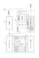
- FIG. 1 is a block diagram showing a configuration example of a light detection device according to a first embodiment of the present technology
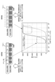
- 4 is a diagram illustrating an example of a histogram generated by a feature extraction unit in the first embodiment of the present technology
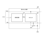
- FIG. 2 is a block diagram showing a configuration example of a readout circuit according to the first embodiment of the present technology
- 1 is a circuit diagram showing a configuration example of a pixel circuit according to a first embodiment of the present technology
- 4 is a timing chart showing an example of an operation of a light receiving unit according to the first embodiment of the present technology.
- FIG. 11 is a block diagram showing a configuration example of a light detection device according to a second embodiment of the present technology.
- FIG. 13 is a block diagram showing a configuration example of a light detection device according to a third embodiment of the present technology.
- FIG. 13 is a block diagram showing a configuration example of a light detection device according to a fourth embodiment of the present technology.
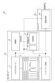
- FIG. 13 is a block diagram showing an example of an arrangement of a light detection device according to a fifth embodiment of the present technology.
- FIG. 23 is a block diagram showing an example of an arrangement of a light detection device according to a sixth embodiment of the present technology.
- FIG. 23 is a block diagram showing an example of an arrangement of a light detection device according to a seventh embodiment of the present technology.
- FIG. 23 is a block diagram showing an example of an arrangement of a light detection device according to an eighth embodiment of the present technology.
- FIG. 23 is a block diagram showing an example of an arrangement of a light detection device according to a ninth embodiment of the present technology.
- 1 is an explanatory diagram of the photon detection interval required for capturing images of high-illuminance and low-illuminance scenes.
- FIG. 11 is an explanatory diagram of a combination of long and short photon detection intervals.
- FIG. 11 is an explanatory diagram of gradation control for each illuminance.
- FIG. 23 is a block diagram showing a configuration example of a light detection device according to a tenth embodiment of the present technology.
- FIG. 23 is a diagram showing a control flow of a gray-scale priority mode (1) of a photodetector according to a tenth embodiment of the present technology.
- FIG. 29 is a diagram showing a control flow of a grayscale priority mode (2) of a photodetector according to a tenth embodiment of the present technology.
- 23 is an explanatory diagram of a low power consumption priority mode of a photodetector according to a tenth embodiment of the present technology;
- FIG. FIG. 23 is a block diagram showing a configuration example of a photodetector according to an eleventh embodiment of the present technology.
- 23 is an explanatory diagram of control of a shutter time of a light detection device according to an eleventh embodiment of the present technology.
- FIG. FIG. 29 is a block diagram showing a configuration example of a light detection device according to a twelfth embodiment of the present technology.
- FIG. 29 is a block diagram showing a configuration example of a photodetector according to a thirteenth embodiment of the present technology.
- FIG. 29 is a diagram illustrating an example of a lookup table according to a thirteenth embodiment of the present technology.
- FIG. 23 is a diagram showing an example of a photon rate for each detection interval in the thirteenth embodiment of the present technology. 23 is a diagram for explaining a method of generating a lookup table in a thirteenth embodiment of the present technology.
- FIG. 26 is a diagram for explaining a method of generating a lookup table in a first modified example of the thirteenth embodiment of the present technology.
- FIG. 1 is a block diagram showing a schematic configuration example of a vehicle control system;
- FIG. 4 is an explanatory diagram showing an example of an installation position of an imaging unit.
- First embodiment an example in which a characteristic signal is detected based on a signal from a pixel array section, and settings of a pulse generator are changed based on the characteristic signal
- Second embodiment an example in which a feature signal is detected based on an image signal generated by an image processing unit, and settings of a pulse generator are changed based on the feature signal
- Third embodiment an example in which a signal from a pixel array section is directly input to a feature extraction section to detect a feature signal, and settings of a pulse generator are changed based on the feature signal
- Fourth embodiment (an example in which, in addition to the configuration of the first embodiment, settings of a pulse generator are controlled based on external user control) 5.
- Fifth embodiment (arrangement example (1) of components of photodetector) 6.
- Sixth embodiment (arrangement example (2) of components of photodetector) 7.
- Seventh embodiment (arrangement example (3) of components of photodetector) 8.
- Eighth embodiment (arrangement example (4) of components of photodetector) 9.
- Ninth embodiment (arrangement example (5) of components of photodetector) 10.
- Tenth embodiment (example of method of performing photon detection at multiple detection intervals, prioritizing gradation and low power consumption) 12.
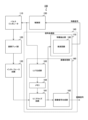
- First embodiment is a block diagram showing a configuration example of a photodetector 100 according to a first embodiment of the present technology.
- the photodetector 100 according to the first embodiment includes a pulse generator 110, a pixel array unit 120, an interface circuit 130, a signal processing unit 140, and a control unit 150.
- the pulse generator 110 Under the control of the control unit 150, the pulse generator 110 generates various pulse signals for driving the pixel array unit 120 and sets the detection interval and number of photon detections.
- the pixel array unit 120 has multiple readout circuits 200 that perform photoelectric conversion, and is an imaging unit that captures images based on the various pulse signals provided by the pulse generator 110.
- the multiple readout circuits 200 are arranged two-dimensionally in a matrix (array), and output a signal according to the number of times incident photons are detected.
- the interface circuit 130 supplies the signal of the pixel array unit 120 to the signal processing unit 140.
- the signal of the pixel array section 120 is an example of an imaging result as described in the claims
- the pixel array section 120 and the interface circuit 130 are an example of an output section as described in the claims
- the pulse generator 110 is an example of a setting section as described in the claims.
- the signal processing unit 140 has an image processing unit 160 and a feature extraction unit 170.
- the image processing unit 160 has a linearization circuit 161 provided at the input stage, and an image signal generation unit 162 provided at the subsequent stage.
- the linearization circuit 161 converts the input signal of the pixel array unit 120 into a linear signal proportional to the illuminance (linearization). During this linearization process, the number of times photons are detected (count number) is converted into an estimated number of incident photons.
- the image signal generation unit 162 generates an image signal based on the signal of the pixel array unit 120 linearized by the linearization circuit 161, and outputs the image signal to the outside of the signal processing unit 140.
- the feature extraction unit 170 has a detection circuit 180.
- the detection circuit 180 receives as input the signal from the pixel array unit 120 linearized by the linearization circuit 161 in the image processing unit 160, and generates a histogram showing the frequency of photon detection as a degree based on that signal.
- An example of a histogram is shown in Figure 2.
- the horizontal axis represents illuminance or the frequency of incident photons (the number of photons during the exposure period), and the vertical axis represents the number of pixels.
- the feature extraction unit 170 extracts feature signals from the output values of the light detection device 100 for determining the features of the image, based on the histogram generated by the detection circuit 180. Specifically, based on the histogram showing the frequency of photon detection as a degree, the feature extraction unit 170 extracts the dynamic range, the maximum value, the minimum value, the average illuminance value, or the median value on the horizontal axis of the histogram as feature signals, and supplies the extracted feature signals to the control unit 150.
- the dynamic range is the difference between the minimum and maximum values on the horizontal axis, i.e., the difference between the minimum and maximum number of photons.
- the average illuminance is the average value of all detection frequencies.
- the median is the median value of the maximum detection frequencies.
- the dynamic range, the maximum value, minimum value, average illuminance, or feature signals such as the median value on the horizontal axis of the histogram are the same in each of the embodiments described below.
- the control unit 150 performs control to change the setting information of the pulse generator 110 based on the feature signal supplied from the feature extraction unit 170. Specifically, the control unit 150 performs control to change at least one of the detection interval and the number of detections of photons in the readout circuit 200, and preferably both the detection interval and the number of detections, as setting information of the pulse generator 110 based on the feature signal. The control unit 150 further performs control over the image processing unit 160.
- Example of the configuration of the readout circuit] 3 is a block diagram showing an example of a configuration of the readout circuit 200 according to the first embodiment of the present technology.
- the readout circuit 200 according to the first embodiment of the present technology includes a pixel circuit 210, a counter 220, and a selection switch 230.
- the pixel circuit 210 generates a pulse signal PLS in response to the incidence of photons and supplies it to the counter 220.
- the counter 220 counts the number of pulses of the pulse signal PLS and supplies the count value to the selection switch 230 as pixel data.
- the count value of the counter 220 is initialized by a reset signal RST supplied from the pulse generator 110 shown in FIG. 1.
- the selection switch 230 performs an on (closed)/off (open) operation according to the selection signal SEL supplied from the pulse generator 110 shown in FIG. 1, and when it is in the on state, it supplies the count value of the counter 220 as pixel data to the signal processing unit 140 shown in FIG. 1.
- Example of pixel circuit configuration is a circuit diagram showing a configuration example of the pixel circuit 210 according to the first embodiment of the present technology.
- the pixel circuit 210 according to the first embodiment of the present technology includes a light detection element 211, a clip transistor 212, an inverter 213, a recharge transistor 214, and a detection circuit 240.
- a pMOS (p-channel Metal Oxide Semiconductor) transistor is used as the clip transistor 212 and the recharge transistor 214.
- the recharge transistor 214 is an example of a recharge unit described in the claims.
- the photodetection element 211 is arranged in an array on a substrate separate from the detection circuit 240. Note that the clip transistor 212, the inverter 213, and a portion of the recharge transistor 214 may be arranged on the same substrate as the photodetection element 211.
- An avalanche photodiode can be used as the light detection element 211.
- An avalanche photodiode that multiplies a single photon by the avalanche phenomenon is called a single photon avalanche diode (SPAD (Single Photon Avalanche Diode)).
- SPAD Single Photon Avalanche Diode
- a SPAD element is used as the light detection element 211.
- a SPAD element is an example of a light detection element as defined in the claims.
- the anode of the light detection element 211 is connected to a node at a predetermined potential lower than the power supply voltage V DD , and the cathode is connected to the clip transistor 212.
- the cathode potential of this light detection element 211 is taken as Vk1.
- the clip transistor 212 and the recharge transistor 214 are connected in series, with the recharge transistor 214 on the power supply voltage V DD side, between the node of the power supply voltage V DD and the cathode of the light detection element 211.
- the potential of the connection node (hereinafter referred to as detection node N1) of these clip transistor 212 and recharge transistor 214 is set to Vk2.
- the control signal CLIP supplied from the pulse generator 110 is input to the gate of the clip transistor 212.
- the control signal XRST supplied from the pulse generator 110 is input to the gate of the recharge transistor 214 and the inverter 213.
- the recharge transistor 214 is connected to the cathode of the light detection element 211, but the recharge transistor 214 may be connected to the anode of the light detection element 211 and the cathode may be connected to a node of the power supply voltage V DD .
- the inverter 213 inverts the logic of the control signal XRST and supplies it to the detection circuit 240.
- the detection circuit 240 detects the incidence of photons and generates a pulse signal PLS.
- This detection circuit 240 includes a pMOS transistor 241, an nMOS (n-channel MOS) transistor 242, an inverter 243, and an inverter 244.
- the pMOS transistor 241 and the nMOS transistor 242 are connected in series between a node of the power supply voltage V DD and a node of the ground voltage, with the pMOS transistor 241 on the power supply voltage V DD side.
- the gate of the pMOS transistor 241 is connected to a detection node N1.
- An inverted signal of the control signal XRST from the inverter 213 is input to the gate of the nMOS transistor 242.
- a signal according to the potential of a connection node N2 between the pMOS transistor 241 and the nMOS transistor 242 is set as a detection signal DET.
- Inverter 243 inverts the logic of the detection signal DET. Inverter 244 inverts the logic of the inverted signal from inverter 243 and supplies it to counter 220 shown in FIG. 3 as a pulse signal PLS.
- setting information for controlling the readout circuit 200 is input to the pulse generator 110 from the control unit 150.
- This setting information includes at least one of the set values for the detection interval and the number of detections for detecting incident photons.
- the detection interval is the period for detecting incident photons
- the detection number indicates the number of times that the control of the detection interval is repeated. Since photon detection is performed over the exposure period, the detection interval x the number of detections is the same value as the exposure period.
- the control unit 150 controls the pulse generator 110 to change the control signal CLIP to high level and then to low level.
- the detection node N1 is disconnected from the cathode of the light detection element 211. This period is hereinafter referred to as the "standby period” during which photons are awaited.
- the detection node N1 is connected to the cathode of the light detection element 211. This period is hereinafter referred to as the "connection period".
- control unit 150 controls the pulse generator 110 to set the control signal XRST to low level for a predetermined period from a predetermined recharge start timing within the connection period. This causes the recharge transistor 214 to supply the power supply voltage V DD to the detection node N1. Since this detection node N1 is connected to the cathode of the light detection element 211, a recharge operation is performed to return the cathode potential Vk1 to the power supply voltage V DD . Furthermore, the detection circuit 240 is initialized by the low-level control signal XRST.
- the clip transistor 212 electrically connects the light detection element 211 and the detection node N1 during the connection period, and disconnects the light detection element 211 from the detection node N1 during the standby period.
- the recharge transistor 214 supplies the power supply voltage V DD to the detection node N1 for a predetermined period from the recharge start timing during the connection period.
- FIG. 5 is a timing chart showing an example of the operation of the pixel circuit 210 according to the first embodiment of the present technology.
- FIG. 5 shows the timing relationship between the control signal CLIP, the control signal XRST, the cathode potential Vk1, the potential Vk2 of the detection node N1, and the output signal of the inverter 213.
- the cathode potential Vk1 and the potential Vk3 of the detection node are both the power supply voltage V DD .
- the pulse generator 110 sets the control signal CLIP to a high level.
- the pulse generator 110 sets the control signal XRST to a high level for a fixed period of time from a predetermined timing within the standby period.
- the thick arrow indicates the timing of photon incidence.
- avalanche multiplication occurs in the light detection element 211, which is made of a SPAD element, and the cathode potential Vk1 drops to a constant potential, at which point the avalanche multiplication stops.
- the detection node N1 is disconnected from the light detection element 211, so the potential Vk2 of the detection node N1 does not oscillate.
- the pulse generator 110 sets the control signal XRST to a low level for a predetermined period from time T2 in the connection period. This causes the power supply voltage V DD to be supplied, and the potential Vk2 of the detection node N1 is initialized to the power supply voltage V DD . In addition, since the detection node N1 is connected to the cathode of the light detection element 211, the cathode potential Vk1 is also initialized to the power supply voltage V DD . At the same time, the detection circuit 240 is initialized, and the pulse signal PLS falls.
- the readout circuit 200 is controlled to transition to a detection state in which it detects photons during the connection period from time T1 to time T2, and to transition to a recharge state during the connection period from time T2 to time T3.
- one pulse can be generated for each detection interval when a photon is incident once or more within the waiting period. For example, in the detection interval from time T3 to time T4, no photons were incident within the waiting period, so no pulse is generated within that connection period. On the other hand, in the detection interval from time T4 to time T5, two photons were incident, so one pulse is generated.
- the configuration example of the readout circuit 200, the configuration example of the pixel circuit 210, and the operation example of the pixel circuit 210 in the first embodiment of the present technology described above are the same in each of the embodiments described below.
- the light detection device 100 in the first embodiment of the present technology includes a readout circuit 200 including a pixel circuit 210 having a light detection element 211 and a recharge transistor 214 that recharges the light detection element 211, and captures images by counting the presence or absence of incident photons at a determined detection interval. Then, at least one of the detection interval and the number of detections of photons is controlled based on the imaging results. More specifically, the linearization circuit 161 in the image processing unit 160 detects a characteristic signal based on the signal of the pixel array unit 120 converted into a linear signal proportional to the illuminance, and at least one of the detection interval and the number of detections of photons is controlled based on the characteristic signal. This makes it possible to optimize the input/output characteristics of the readout circuit 200 (i.e., the number of incident photons - the characteristics of the count value of the counter 220), and accordingly to provide an appropriate dynamic range for the incident light.
- the input/output characteristics of the readout circuit 200 i.
- the capacitance of the cathode of the photodetection element 211 which is made of a SPAD element, can be reduced by the action of the clip transistor 212, which connects/disconnects (isolates) the cathode of the photodetection element 211 to the detection node N1. This makes it possible to reduce power consumption.
- FIG. 6 is a block diagram showing a configuration example of a light detection device 100 according to the second embodiment of the present technology.
- the photodetector 100 in the first embodiment of the present technology is configured to input the signal of the pixel array section 120, which has been converted into a linear signal proportional to the illuminance by the linearization circuit 161 in the image processing section 160, to the feature extraction section 170.
- the photodetector 100 in the second embodiment of the present technology is configured to input the image signal generated by the image signal generation section 162 in the image processing section 160 to the feature extraction section 170.
- the image processing unit 160 has a linearization circuit 161 and an image signal generation unit 162. Based on the signal from the pixel array unit 120 that has been converted into a linear signal proportional to the illuminance by the linearization circuit 161, the image signal generation unit 162 generates an image signal and outputs it to the outside of the signal processing unit 140.
- the detection circuit 180 receives the image signal generated by the image signal generation unit 162 in the image processing unit 160 as input, and generates a histogram indicating the frequency of photon detection as a degree based on the pixel signal.
- the feature extraction unit 170 then extracts the dynamic range, average illuminance value, or median value as a feature signal based on the histogram generated by the detection circuit 180, and supplies the extracted feature signal to the control unit 150.
- the control unit 150 performs control to change at least one of the detection interval and the number of detections of photons in the readout circuit 200, and preferably both the detection interval and the number of detections, as setting information for the pulse generator 110, based on the feature signal supplied from the feature extraction unit 170.
- a feature signal is detected based on the image signal generated by the image processor 160, and at least one of the detection interval and the number of photon detections is controlled based on the feature signal.
- FIG. 7 is a block diagram showing a configuration example of a light detection device 100 according to the third embodiment of the present technology.
- the photodetector 100 in the third embodiment of the present technology is configured to input the signal of the pixel array section 120 output from the interface circuit 130 directly to the feature extraction section 170.
- the feature extraction section 170 is configured to have a linearization circuit 190 in the stage preceding the detection circuit 180, i.e., in the input stage.
- the linearization circuit 190 linearizes the input signal of the pixel array section 120 into a linear signal proportional to the illuminance, similar to the linearization circuit 161 provided in the image processing section 160 of the photodetector 100 in the first embodiment of the present technology.
- the detection circuit 180 In the feature extraction unit 170, the detection circuit 180 generates a histogram showing the frequency of photon detection as a degree based on the signal of the pixel array unit 120 that has been converted into a linear signal proportional to the illuminance by the linearization circuit 190. The feature extraction unit 170 then extracts a feature signal of the output value of the light detection device 100 based on the histogram generated by the detection circuit 180, and supplies this extracted feature signal to the control unit 150.
- the control unit 150 performs control to change at least one of the detection interval and the number of detections of photons in the readout circuit 200, and preferably both the detection interval and the number of detections, as setting information for the pulse generator 110, based on the feature signal supplied from the feature extraction unit 170.
- the light detection device 100 in the third embodiment of the present technology has a linearization circuit 190 at the input stage of the feature extraction unit 170, and the signal of the pixel array unit 120 output from the interface circuit 130 is directly input to the feature extraction unit 170. Then, in the feature extraction unit 170, a feature signal is detected based on the signal of the pixel array unit 120 that has been linearized to a linear signal proportional to the illuminance, and at least one of the detection interval and the number of detections of photons is controlled based on the feature signal, thereby optimizing the input/output characteristics of the readout circuit 200 as in the first embodiment, and accordingly an appropriate dynamic range can be achieved for the incident light.
- FIG. 8 is a block diagram showing a configuration example of a light detection device 100 according to the fourth embodiment of the present technology.
- the photodetector 100 in the fourth embodiment of the present technology is based on the photodetector 100 in the first embodiment of the present technology, and is configured such that the control unit 150 controls at least one of the detection interval and the number of detections of photons by changing the setting information of the pulse generator 110 based on the feature signal detected by the feature extraction unit 170.
- the photodetector 100 in the fourth embodiment of the present technology is configured such that the control unit 150 controls at least one of the detection interval and the number of detections of photons based on external user control.
- External control by the user (user control) of the control unit 150 can be performed via a bus such as I2C (Inter-Integrated Circuit), I3C (Improved Inter-Integrated Circuit), or SPI (Serial Peripheral Interface).
- I2C Inter-Integrated Circuit
- I3C Improved Inter-Integrated Circuit
- SPI Serial Peripheral Interface
- the setting information of the pulse generator 110 can be changed based on a feature signal detected based on the imaging results, and the setting information of the pulse generator 110 can be changed arbitrarily based on external control by the user.
- a system configuration can be provided in which a mode of manual control by a user, a mode of automatic control based on imaging results, and a mode of control based on limitations set by the user and imaging results can be switched.
- limitations set by the user include dynamic range, shutter time, frame rate, SNR (Signal-to-Noise Ratio), gamma curve characteristics, etc.
- Example of arrangement of components of a light detection device (1) 9 is a block diagram showing an example of the arrangement of the light detection device 100 according to the fifth embodiment of the present technology.
- the example of the arrangement of the light detection device 100 according to the fifth embodiment of the present technology is based on the configuration of the light detection device 100 according to the first embodiment of the present technology.
- An example of the layout of the optical detection device 100 in the fifth embodiment of the present technology is a configuration in which the pulse generator 110, pixel array section 120, and interface circuit 130 in the optical detection device 100 in the first embodiment are arranged on a sensor chip 300, and the control section 150, image processing section 160, and feature extraction section 170 are arranged on an ISP (Image Signal Processor) chip 400.
- the sensor chip 300 is an example of the first chip described in the claims
- the ISP chip 400 is an example of the second chip described in the claims.
- the image processing unit 160 and the feature extraction unit 170 are arranged on the ISP chip 400, it is possible to obtain the same action and effect as the light detection device 100 in the first embodiment of the present technology. That is, since at least one of the detection interval and the number of detections of photons can be controlled based on the feature signal detected based on the imaging results, it is possible to optimize the input/output characteristics of the readout circuit 200, and accordingly, an appropriate dynamic range can be obtained for the incident light.
- Sixth embodiment is a block diagram showing an example of the arrangement of the light detection device 100 according to the sixth embodiment of the present technology.
- the example of the arrangement of the light detection device 100 according to the sixth embodiment of the present technology is based on the configuration of the light detection device 100 according to the second embodiment of the present technology.
- An example of the layout of the photodetector 100 in the sixth embodiment of the present technology is a configuration in which the pulse generator 110, pixel array section 120, and interface circuit 130 in the photodetector 100 in the second embodiment of the present technology are arranged on the sensor chip 300, the image processing section 160 is arranged on the ISP chip 400, and the control section 150 and feature extraction section 170 are arranged on a control chip 500 that is different from the ISP chip 400.
- the control chip 500 is an example of the third chip described in the claims.
- control unit 150 and the feature extraction unit 170 are arranged on the control chip 500, which is a chip separate from the ISP chip 400, it is possible to obtain the same action and effect as the light detection device 100 in the first embodiment of the present technology.
- the control unit 150 and the feature extraction unit 170 are arranged on the control chip 500, which is a chip separate from the ISP chip 400, it is possible to obtain the same action and effect as the light detection device 100 in the first embodiment of the present technology.
- at least one of the detection interval and the number of detections of photons can be controlled based on the feature signal detected based on the imaging results, it is possible to optimize the input/output characteristics of the readout circuit 200, and accordingly, an appropriate dynamic range can be obtained for the incident light.
- Seventh embodiment is a block diagram showing an example of the arrangement of the light detection device 100 according to the seventh embodiment of the present technology.
- the example of the arrangement of the light detection device 100 according to the seventh embodiment of the present technology is based on the configuration of the light detection device 100 according to the third embodiment of the present technology.
- An example of the layout of the photodetector 100 in the seventh embodiment of the present technology is a configuration in which the control unit 150 and the feature extraction unit 170 are arranged on the same sensor chip 300 as the pulse generator 110, the pixel array unit 120, and the interface circuit 130 in the photodetector 100 in the third embodiment of the present technology, and the image processing unit 160 is arranged on the ISP chip 400.
- control unit 150 and the feature extraction unit 170 are arranged on the same sensor chip 300 as the pixel array unit 120, it is possible to obtain the same action and effect as the light detection device 100 in the first embodiment of the present technology.
- at least one of the detection interval and the number of detections of photons can be controlled based on the feature signal detected based on the imaging results, it is possible to optimize the input/output characteristics of the readout circuit 200, and accordingly, an appropriate dynamic range can be obtained for the incident light.
- Eighth embodiment [Example of arrangement of components of a light detection device (4)] 12 is a block diagram showing an example of the arrangement of the light detection device 100 according to the eighth embodiment of the present technology.
- the example of the arrangement of the light detection device 100 according to the eighth embodiment of the present technology is based on the configuration of the light detection device 100 according to the first embodiment of the present technology.
- the pulse generator 110, pixel array section 120, and interface circuit 130 in the photodetector 100 in the first embodiment of the present technology are arranged on the sensor chip 300, the image processing section 160 and feature extraction section 170 are arranged on the ISP chip 400, and only the control section 150 is arranged on the control chip 500.
- control unit 150 is arranged on the control chip 500, which is a chip separate from the sensor chip 300 and the ISP chip 400, it is possible to obtain the same action and effect as the light detection device 100 in the first embodiment of the present technology. That is, since at least one of the detection interval and the number of detections of photons can be controlled based on a characteristic signal detected based on the imaging results, it is possible to optimize the input/output characteristics of the readout circuit 200, and accordingly, an appropriate dynamic range can be obtained for the incident light.
- Ninth embodiment is a block diagram showing an example of the arrangement of the light detection device 100 according to the ninth embodiment of the present technology.
- the example of the arrangement of the light detection device 100 according to the ninth embodiment of the present technology is based on the configuration of the light detection device 100 according to the first embodiment of the present technology.
- An example of the layout of the photodetector 100 in the ninth embodiment of the present technology is a configuration in which the control unit 150 is arranged on the same sensor chip 300 as the pulse generator 110, pixel array unit 120, and interface circuit 130 in the photodetector 100 in the first embodiment of the present technology, and the image processing unit 160 and feature extraction unit 170 are arranged on the ISP chip 400.
- control unit 150 is arranged on the same sensor chip 300 as the pixel array unit 120, it is possible to obtain the same action and effect as the light detection device 100 in the first embodiment of the present technology. That is, since at least one of the detection interval and the number of detections of photons can be controlled based on a characteristic signal detected based on the imaging results, it is possible to optimize the input/output characteristics of the readout circuit 200, and accordingly, an appropriate dynamic range can be obtained for the incident light.
- the illuminance range in which the counter count value has a gradation is restricted by the photon detection interval.
- the illuminance range is the dynamic range of illuminance, ranging from the darkest to the brightest in the entire image.
- FIG. 14 is an explanatory diagram of the photon detection intervals required for shooting scenes with high and low illumination.
- One imaging frame is made up of a relatively long photon detection interval and a relatively short photon detection interval. If one or more photons are incident within one detection interval, the count value (number of counts) becomes “1". Even if multiple photons are incident within one detection interval, the count value is still "1".
- the lower diagram in Figure 14 shows the input/output characteristics, with the horizontal axis representing the incident photon rate proportional to illuminance, and the vertical axis representing the count value.
- the solid curve shows the case of a relatively long photon detection interval (e.g., 1000 [nsec] x 5000 [cnt])
- the dotted curve shows the case of a relatively short photon detection interval (e.g., 10 [nsec] x 5000 [cnt]).
- the part where the curve has gradation corresponds to the dynamic range.
- the dynamic range can only be secured in areas of relatively low illuminance, or the dynamic range can only be secured in areas of relatively high illuminance.
- Fig. 15 is an explanatory diagram of combinations of long and short photon detection intervals.
- the lower diagram in Fig. 15 shows input/output characteristics with the horizontal axis representing the incident photon rate and the vertical axis representing the count value.
- the solid curve shows the case of a relatively long photon detection interval (e.g., 1000 [nsec] x 5000 [cnt])
- the dotted curve shows the case of a relatively short photon detection interval (e.g., 10 [nsec] x 5000 [cnt]).
- the characteristics when long and short detection intervals are combined are shown by dashed curves.
- the blend ratio of the number of detections (counts) for each long and short detection interval can also be changed. In this way, by changing the blend ratio of the number of detections for each long and short detection interval, it is possible to control the gradation for each illuminance.
- Fig. 16 is an explanatory diagram of gradation control for each illuminance.
- Fig. 16 shows input/output characteristics with the horizontal axis representing the incident photon rate and the vertical axis representing the count value.
- the solid curve shows the case of a relatively long detection interval
- the dotted curve shows the case of a relatively short detection interval
- the dashed line shows the case of a combination of long and short detection intervals.
- a relatively long detection interval is 10 [nsec] x 500 [cnt] + 100 [nsec] x 4000 [cnt] + 1000 [nsec] x 500 [cnt]
- a relatively short detection interval is 10 [nsec] x 4000 [cnt] + 100 [nsec] x 500 [cnt] + 1000 [nsec] x 500 [cnt]
- a combination of long and short detection intervals is 10 [nsec] x 500 [cnt] + 100 [nsec] x 500 [cnt] + 1000 [nsec] x 4000 [cnt].
- the gradation for each illuminance can be controlled by changing the blend ratio of the number of detections (count numbers) for each long and short detection interval. For example, if it is desired to obtain gradation on the relatively high illuminance side, the number of detections at relatively short detection intervals is increased, and if it is desired to obtain gradation on the relatively low illuminance side, the number of detections at relatively long detection intervals is increased. This increases the gradation in the corresponding illuminance region, thereby improving the SNR.
- the tenth embodiment of the present technology is an example in which priority is given to gradation and low power consumption in a method of performing photon detection at a plurality of detection intervals.
- the tenth embodiment of the present technology is also an example in which all processes from detection of a signal from the pixel array unit 120 to control of at least one of the detection interval and the number of detections of photons based on the detection result are performed on the application processor side, which will be described later.
- FIG. 17 is a block diagram showing a configuration example of a light detection device 100 according to the tenth embodiment of the present technology.
- the photodetector 100 in the tenth embodiment of the present technology includes a pulse generator 110, a pixel array section 120, an interface circuit 130, a signal processing section 140, and a control section 150, and the pulse generator 110, the pixel array section 120, and the interface circuit 130 are arranged on a sensor chip 300.
- the signal processing section 140, which includes an image processing section 160 and a feature extraction section 170, and the control section 150 constitute an application processor 600.
- the feature extraction unit 170 has a detection circuit 180 and a target sensor response curve design unit 610.
- the detection circuit 180 generates a histogram showing the frequency of photon detection as a frequency based on the signal from the pixel array section 120 that has been linearized into a linear signal proportional to the illuminance by the linearization circuit 161 in the image processing section 160, and creates a frequency distribution (illuminance distribution) of the photon rate from the histogram.
- the target sensor response curve design unit 610 creates a target sensor response curve based on the frequency distribution of the photon rate created by the detection circuit 180, and supplies information about the target sensor response curve to the control unit 150 as a feature signal.
- control unit 150 When the control unit 150 receives information on a target sensor response curve from the target sensor response curve design unit 610, it estimates the photon detection interval T p that realizes the sensor response curve and the count value (number of counts) N max at a certain photon detection interval. That is, the control unit 150 has a function of calculating the photon detection interval T p and the count value (number of photon detections) N max .
- the control unit 150 controls at least one of the photon detection interval and the number of detections by providing the estimated photon detection interval T p and the count value N max at a certain photon detection interval to the pulse generator 110.
- the application processor 600 which includes the image processing unit 160, the feature extraction unit 170, and the control unit 150, detects feature signals in the image capture results from the pixel array unit 120, and outputs a signal for controlling at least one of the detection interval and the number of detections of photons in the light detection element 211 based on the feature signals.
- FIG. 18 is a diagram showing a control flow of the grayscale priority mode (1) of the photodetector 100 according to the tenth embodiment of the present technology.
- a in FIG. 18 represents the entire image of a certain scene.
- the detection circuit 180 creates a frequency distribution of the photon rate from a histogram showing the frequency of photon detection as a frequency.
- the frequency distribution of the photon rate is shown in B in FIG. 18.
- the target sensor response curve design unit 610 creates a target sensor response curve. Specifically, a sensor response curve is created in which the slope of the count value is steep where the frequency distribution of the photon rate is high and the slope of the count value is shallow where the frequency distribution of the photon rate is low.
- the target sensor response curve is shown in C in FIG.
- the control unit 150 estimates the photon detection interval T p that realizes the target sensor response curve and the count value N max at a certain photon detection interval, as shown in D in FIG. 18.
- gradation priority mode (1) under the control of the control unit 150 shown in FIG. 17, a histogram of the illuminance distribution (frequency distribution of the photon rate) of the entire image of a certain scene is referenced, and control is performed to increase the gradation in the illuminance range with a high frequency distribution, that is, to maximize the gradation of the photon count value (number of detections) for the illuminance distribution of the scene.
- control that prioritizes the gradation of the photon count value, it becomes possible to control the photon detection interval and photon count value appropriately for the illuminance distribution of the scene, and it is possible to obtain maximum scene information.
- tone priority mode (1) is intended to control the gradation of the photon count value (detection count) to maximize the gradation of the illuminance distribution of the entire image of a certain scene
- tone priority mode (2) is intended to control the gradation of the photon count value (detection count) to maximize the gradation of the illuminance distribution of the target subject.
- FIG. 19 is a diagram showing the control flow of the gradation priority mode (2) of the photodetector 100 in the tenth embodiment of the present technology.
- a indicates the area (dashed line frame) of the target subject.
- the detection circuit 180 creates a frequency distribution of the photon rate from a histogram showing the frequency of photon detection as a frequency. Specifically, a frequency distribution of the photon rate weighted for the area of the target subject is created. The frequency distribution of the photon rate is shown in FIG. 19, b.
- the target sensor response curve design unit 610 creates a target sensor response curve. Specifically, a sensor response curve is created in which the slope of the count value is large where the frequency distribution of the photon rate is high and the slope of the count value is small where the frequency distribution of the photon rate is low.
- the target sensor response curve is shown in FIG. 19, c.
- the control unit 150 estimates the photon detection interval T p that realizes the target sensor response curve and the count value N max at a certain photon detection interval, as shown in FIG. 19, d.
- gradation priority mode (2) under the control of the control unit 150 shown in FIG. 17, a histogram of the illuminance distribution (frequency distribution of the photon rate) in the area of the target subject is referenced, and control is performed to maximize the gradation of the photon count value (number of detections) for that illuminance distribution.
- control is performed to maximize the gradation of the photon count value (number of detections) for that illuminance distribution.
- FIG. 20 is an explanatory diagram of the low power consumption priority mode of the photodetector 100 in the tenth embodiment of the present technology.
- the SNR curve for a single detection interval is given by the following equation: In the above formula, f p is the incident photon rate, T p is the detection interval of photons, and N max is the number of times photons are detected (count value of the counter).
- the control unit 150 shown in Fig. 17 when SNR curves of a plurality of detection intervals Tp are plotted, control is performed to minimize the count value (number of photon detections) of the counter 220 within a range that does not fall below the minimum required SNR within the illuminance range of the scene. This makes it possible to reduce the power consumption of the photodetector 100.
- the minimum required SNR within the illuminance range of the scene is set to 25 [dB].
- the eleventh embodiment of the present technology is an example of controlling the shutter time in a method of performing photon detection at a plurality of detection intervals.
- a target sensor response curve (gradation) created based on the frequency distribution of the photon rate is fixed, and control is performed to shift only the dynamic range.
- FIG. 21 is a block diagram showing a configuration example of a light detection device 100 according to the eleventh embodiment of the present technology.
- the photodetector 100 in the eleventh embodiment of the present technology includes a pulse generator 110, a pixel array section 120, an interface circuit 130, a signal processing section 140, and a control section 150, and the pulse generator 110, the pixel array section 120, and the interface circuit 130 are arranged on a sensor chip 300.
- the signal processing section 140, which includes an image processing section 160 and a feature extraction section 170, and the control section 150 constitute an application processor 600.
- the gradation shape of the sensor response curve
- the feature extraction unit 170 has only the detection circuit 180. That is, in the eleventh embodiment, the target sensor response curve design unit 610 that was disposed in the feature extraction unit 170 in the tenth embodiment is not required.
- the configuration of the application processor 600 in the eleventh embodiment can be simplified compared to the tenth embodiment by the amount that the target sensor response curve design unit 610 is not required.
- the detection circuit 180 generates a histogram showing the frequency of photon detection as a frequency based on the signal from the pixel array unit 120 that has been linearized to a linear signal proportional to the illuminance by the linearization circuit 161 in the image processing unit 160, and creates a frequency distribution (illuminance distribution) of the photon rate as a signal statistic from the histogram.
- the detection circuit 180 then supplies the signal statistic after detection to the control unit 150 as a feature signal.
- control unit 150 When the control unit 150 receives the frequency distribution of the photon rate as a feature signal from the detection circuit 180, it estimates the photon detection interval T p that realizes a fixed sensor response curve and the count value (number of counts) N max at a certain photon detection interval. That is, the control unit 150 has a function of calculating the photon detection interval T p and the count value (number of times a photon is detected) N max .
- the control unit 150 performs control to uniformly multiply the detection intervals Tp of all photons by n.
- the multiple detection intervals Tp are set to 25 [nsec] (large dotted line in the figure), 100 [nsec] (large dashed line), 400 [nsec] (two-dotted line), 1600 [nsec] (small dotted line), 6400 [nsec] (small dashed line), and 25600 [nsec] (dotted line), which is the same as the low power consumption priority mode in the tenth embodiment of the present technology.
- the dynamic range of the input photon rate shifts by 1/n.
- the dynamic range of the input photon rate shifts from 104 to 108 [Hz] to 105 to 109 [Hz], as shown in FIG.
- control is performed to shift only the dynamic range without changing the shape of the sensor response curve created based on the frequency distribution of the photon rate created by the detection circuit 180. This makes it possible to shift only the dynamic range while keeping the gradation fixed by not changing the shape of the sensor response curve.
- FIG. 23 is a block diagram showing a configuration example of a light detection device 100 according to the twelfth embodiment of the present technology.
- the photodetector 100 in the twelfth embodiment of the present technology includes a pulse generator 110, a pixel array unit 120, an interface circuit 130, an image processor 160, a detection circuit 180, a target sensor response curve design unit 610, and a control unit 150, and the image processor 160 and the detection circuit 180 form an application processor 600.
- the pulse generator 110, the pixel array unit 120, the interface circuit 130, the target sensor response curve design unit 610, and the control unit 150 are arranged on the sensor chip 300 side.
- the photodetector 100 in the twelfth embodiment of the present technology is configured to output the signal statistics after detection by the detection circuit 180 in the application processor 600 to the sensor chip 300, and the processing subsequent to the design of the sensor response curve by the target sensor response curve design unit 610 is performed on the sensor chip 300 side. Even with this configuration, it is possible to perform processing similar to the two gradation priority modes (1) and (2) and the low power consumption priority mode in the twelfth embodiment of the present technology.
- the twelfth embodiment of the present technology is a modified version of the tenth embodiment of the present technology, it can also be a modified version of the eleventh embodiment of the present technology.
- the target sensor response curve design unit 610 in FIG. 23 is deleted.
- the linearization circuit 161 linearizes the signal from the pixel array unit 120.
- the control unit 150 tries to control the detection interval or the number of detections in accordance with the imaging scene, the response characteristics of the pixel array unit 120 also change. For this reason, in order to perform linearization in accordance with the scene, an inverse function of a function indicating the response characteristics is required.
- the photodetection device 100 in this thirteenth embodiment differs from the first embodiment in that a lookup table is generated using an inverse function.
- FIG. 24 is a block diagram showing an example of a configuration of a light detection device 100 in a thirteenth embodiment of the present technology.
- the light detection device 100 in this thirteenth embodiment differs from the first embodiment in that a lookup table generation unit 163 and a memory 164 are further arranged in the image processing unit 160.
- the lookup table generating unit 163 generates a lookup table in which the photon count value N cnt from the pixel array unit 120 corresponds to the photon rate f p based on the detection interval T p and the number of detections set by the control unit 150.
- the response characteristic of the pixel array unit 120 to the incidence of photons is nonlinear.
- a function indicating this response characteristic can be expressed by, for example, the following equation.
- N max is the total count number, and when counting from "0", it is a value obtained by subtracting "1" from the set value of the number of detections.
- Equation 2 The inverse function of Equation 2 is expressed by the following equation.
- the lookup table generating unit 163 calculates the photon rate fp for each count value Ncnt using Equation 3, generates a lookup table correlating them, and stores it in the memory 164.
- the linearization circuit 161 refers to the lookup table stored in the memory 164, acquires the photon rate fp corresponding to the count value Ncnt , and supplies it to the feature extraction unit 170 and the image signal generating unit 162. In this way, linearization is realized.
- 25 is a diagram showing an example of a lookup table in the thirteenth embodiment of the present technology.
- the range of the count value N cnt is from “0" to "4999”.
- the lookup table generating unit 163 substitutes each of "0" to "4999", the total count number N max (here, 4999), and the set detection interval T p into Equation 3 to calculate the photon rate f p for values of "f 0 " to "f 4999 ". Then, the lookup table generating unit 163 causes the memory 164 to hold a lookup table in which the count values and the photon rates are associated with each other.
- control unit 150 can set a plurality of detection intervals for the purpose of expanding the dynamic range, etc.
- An example of a method for generating a lookup table when a plurality of detection intervals are set will be described with reference to Figures 26 and 27.
- the range of count values N cnt (1) corresponding to detection interval T p1 is from “0” to “7”
- the range of count values N cnt (2) corresponding to detection interval T p2 is from “0” to "5".
- the range of count values N cnt (3) corresponding to detection interval T p3 is from “0" to "4". According to equation 3, the photon rate when the count value is "0" is "0" regardless of the detection interval. Therefore, the lookup table generator 163 calculates the photon rate for each count value after "1" for each detection interval using the inverse function of equation 3.
- the photon rate fp (1) corresponding to the detection interval Tp1 was calculated to be between “3” and “105”
- the photon rate fp (2) corresponding to the detection interval Tp2 was calculated to be between "1.1” and "23”
- the photon rate fp (3) corresponding to the detection interval Tp3 was calculated to be between "0.3” and "5".
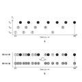
- FIG. 27a An example of the photon rate for each detection interval is shown in Fig. 27a.
- the vertical axis of Fig. 27a indicates the detection interval, and the horizontal axis indicates the photon rate.
- the black circles indicate the calculated value of the photon rate fp (1)
- the gray circles indicate the calculated value of the photon rate fp (2)
- the white circles indicate the calculated value of the photon rate fp (3) .
- the numbers in the circles indicate the corresponding count values.
- the lookup table generating unit 163 sorts the set of photon rates calculated for each detection interval according to a predetermined rule (for example, in ascending order).
- the set f p cat of photon rates before sorting is expressed by, for example, the following formula.
- the set from 0.3 to 105 corresponds to f p (1)
- 1.1 to 23 corresponds to f p (2)
- 0.3 to 5 corresponds to f p (3) .
- the set of sorted photon rates fp is expressed, for example, by the following formula:
- the lookup table generator 163 assigns a new count value to each of the sorted photon rates.
- the total number of calculated photon rate values is 16, so count values from "1" to “16" are assigned.
- the minimum value of the photon rate in Equation 5 is "0.3”, so that value is assigned a count value of "1".
- the maximum value of the photon rate in Equation 5 is "105”, so that value is assigned a count value of "16”.
- the lookup table generator 163 generates a lookup table that associates these count values with the photon rates. However, as this results in some error, it is preferable to correct the photon rate value using Newton's method.
- the calculated value of the formula 5 is used as the initial value f p — 0. Furthermore, based on the formula 2, the following function f(x) is defined.
- I is an integer indicating the number of detection intervals set, and in the example of formula 4, it is "3".
- the lookup table generating unit 163 repeats the following equation for each count value until t reaches a predetermined value (for example, "2"), to find a convergence value.
- a predetermined value for example, "2”
- the value of Equation 5 is used as the initial value f p — 0 when t is “0”.
- the lookup table generation unit 163 uses the convergence value obtained from Equation 8 for each count value as the corrected photon rate and updates the lookup table with that value.
- the lookup table generating unit 163 generates a lookup table using an inverse function, so that the linearization circuit 161 can refer to the table and perform appropriate linearization according to the scene.
- the lookup table generator 163 calculates and sorts the photon rate for each detection interval, and assigns a count value, but it is desirable to further reduce the amount of calculation.
- the photodetector in this modified example of the thirteenth embodiment differs from the first embodiment in that a plurality of lookup tables created in advance are combined.
- FIG. 28 is a diagram for explaining a method of generating a lookup table in a modified example of the thirteenth embodiment of the present technology.
- a plurality of lookup tables with different detection intervals that have been generated in advance are stored in the memory 164 as a combination source lookup table.
- a shows an example of a combination source lookup table when a detection interval Ta and a detection count of "10000" are set.
- photon rates corresponding to count values from "0" to "9999" are f a0 to f a9999 .
- b shows an example of a combination source lookup table when a detection interval Tb and a detection count of "10000" are set.
- photon rates corresponding to count values from "0" to "9999" are f b0 to f b9999 .
- the number of combination source lookup tables in memory 164 is not limited to two, and may be three or more.
- the lookup table generation unit 163 When the control unit 150 sets the detection interval and the number of detections, the lookup table generation unit 163 reads out from the memory 164 a plurality of combination source lookup tables having detection intervals close to the set detection interval. The lookup table generation unit 163 then generates a new lookup table as a combination destination lookup table by weighting and adding up those photon rates.
- the detection interval set during imaging is Tc, and the following relational expressions are established between Tc, Ta, and Tb.
- ⁇ and ⁇ are real numbers and are used as weights.
- the lookup table generating unit 163 reads f a0 from the table a in the figure for the photon rate corresponding to the count value "0", and reads f b0 from the table b in the figure. Then, the lookup table generating unit 163 performs weighted addition of these photon rates using weights ⁇ and ⁇ , and sets the added value as the photon rate corresponding to the count value "0" in the combination source lookup table. The same weighted addition is performed for count values "1" and onwards. In this way, in the modified example of the thirteenth embodiment, a combination source lookup table generated in advance is used, so that the amount of calculation can be reduced compared to the thirteenth embodiment.
- the number of detections in the combined lookup table generated in c in the figure may be greater than the number of detections set by the control unit 150.
- the lookup table generating unit 163 thins out the rows (count values and photon rates) of c in the figure in accordance with the set value.
- the detection count in the join source lookup table of c in the figure is "10000" and the set detection count is "5000"
- half of the rows are thinned out.
- d in the figure shows an example of the table after thinning.
- the shaded rows in d in the figure indicate the thinned rows.
- the rows in c in the figure that had odd count values are thinned out.
- new count values from "0" to "4999" are assigned to the remaining rows.
- the combined lookup table of c in the figure is stored in memory 164, and if thinning is required, the combined lookup table of d in the figure is stored in memory 164.
- the linearization circuit 161 performs linearization by referring to the combined lookup table.
- an approximate solution for the photon rate for each count value can be obtained based on multiple inverse function equations using a bulb algorithm such as bisection.
- the lookup table generation unit 163 determines the destination lookup table by performing a weighted addition of multiple source lookup tables, thereby reducing the amount of calculations.
- the technology according to the present disclosure can be applied to various products.
- the technology according to the present disclosure may be realized as a device mounted on any type of moving body such as an automobile, an electric vehicle, a hybrid electric vehicle, a motorcycle, a bicycle, a personal mobility device, an airplane, a drone, a ship, or a robot.
- FIG. 29 is a block diagram showing a schematic configuration example of a vehicle control system, which is an example of a mobile object control system to which the technology disclosed herein can be applied.
- the vehicle control system 12000 includes a plurality of electronic control units connected via a communication network 12001.
- the vehicle control system 12000 includes a drive system control unit 12010, a body system control unit 12020, an outside vehicle information detection unit 12030, an inside vehicle information detection unit 12040, and an integrated control unit 12050.
- Also shown as functional components of the integrated control unit 12050 are a microcomputer 12051, an audio/video output unit 12052, and an in-vehicle network I/F (interface) 12053.
- the drive system control unit 12010 controls the operation of devices related to the drive system of the vehicle according to various programs.
- the drive system control unit 12010 functions as a control device for a drive force generating device for generating the drive force of the vehicle, such as an internal combustion engine or a drive motor, a drive force transmission mechanism for transmitting the drive force to the wheels, a steering mechanism for adjusting the steering angle of the vehicle, and a braking device for generating a braking force for the vehicle.
- the body system control unit 12020 controls the operation of various devices installed in the vehicle body according to various programs.
- the body system control unit 12020 functions as a control device for a keyless entry system, a smart key system, a power window device, or various lamps such as headlamps, tail lamps, brake lamps, turn signals, and fog lamps.
- radio waves or signals from various switches transmitted from a portable device that replaces a key can be input to the body system control unit 12020.
- the body system control unit 12020 accepts the input of these radio waves or signals and controls the vehicle's door lock device, power window device, lamps, etc.
- the outside-vehicle information detection unit 12030 detects information outside the vehicle equipped with the vehicle control system 12000.
- the image capturing unit 12031 is connected to the outside-vehicle information detection unit 12030.
- the outside-vehicle information detection unit 12030 causes the image capturing unit 12031 to capture images outside the vehicle, and receives the captured images.
- the outside-vehicle information detection unit 12030 may perform object detection processing or distance detection processing for people, cars, obstacles, signs, or characters on the road surface, based on the received images.
- the imaging unit 12031 is an optical sensor that receives light and outputs an electrical signal according to the amount of light received.
- the imaging unit 12031 can output the electrical signal as an image, or as distance measurement information.
- the light received by the imaging unit 12031 may be visible light, or may be invisible light such as infrared light.
- the in-vehicle information detection unit 12040 detects information inside the vehicle.
- a driver state detection unit 12041 that detects the state of the driver is connected.
- the driver state detection unit 12041 includes, for example, a camera that captures an image of the driver, and the in-vehicle information detection unit 12040 may calculate the driver's degree of fatigue or concentration based on the detection information input from the driver state detection unit 12041, or may determine whether the driver is dozing off.
- the microcomputer 12051 can calculate control target values for the driving force generating device, steering mechanism, or braking device based on information inside and outside the vehicle acquired by the outside vehicle information detection unit 12030 or the inside vehicle information detection unit 12040, and output control commands to the drive system control unit 12010.
- the microcomputer 12051 can perform cooperative control aimed at realizing the functions of an Advanced Driver Assistance System (ADAS), including vehicle collision avoidance or impact mitigation, following driving based on the distance between vehicles, maintaining vehicle speed, vehicle collision warning, or vehicle lane departure warning.
- ADAS Advanced Driver Assistance System
- the microcomputer 12051 can also perform cooperative control for the purpose of autonomous driving, which allows the vehicle to travel autonomously without relying on the driver's operation, by controlling the driving force generating device, steering mechanism, braking device, etc. based on information about the surroundings of the vehicle acquired by the outside vehicle information detection unit 12030 or the inside vehicle information detection unit 12040.
- the microcomputer 12051 can also output control commands to the body system control unit 12020 based on information outside the vehicle acquired by the outside-vehicle information detection unit 12030. For example, the microcomputer 12051 can control the headlamps according to the position of a preceding vehicle or an oncoming vehicle detected by the outside-vehicle information detection unit 12030, and perform cooperative control aimed at preventing glare, such as switching from high beams to low beams.
- the audio/image output unit 12052 transmits at least one output signal of audio and image to an output device capable of visually or audibly notifying the occupants of the vehicle or the outside of the vehicle of information.
- an audio speaker 12061, a display unit 12062, and an instrument panel 12063 are exemplified as output devices.
- the display unit 12062 may include, for example, at least one of an on-board display and a head-up display.
- FIG. 30 shows an example of the installation position of the imaging unit 12031.
- the imaging unit 12031 includes imaging units 12101, 12102, 12103, 12104, and 12105.
- the imaging units 12101, 12102, 12103, 12104, and 12105 are provided, for example, at the front nose, side mirrors, rear bumper, back door, and upper part of the windshield inside the vehicle cabin of the vehicle 12100.
- the imaging unit 12101 provided at the front nose and the imaging unit 12105 provided at the upper part of the windshield inside the vehicle cabin mainly acquire images of the front of the vehicle 12100.
- the imaging units 12102 and 12103 provided at the side mirrors mainly acquire images of the sides of the vehicle 12100.
- the imaging unit 12104 provided at the rear bumper or back door mainly acquires images of the rear of the vehicle 12100.
- the imaging unit 12105 provided at the upper part of the windshield inside the vehicle cabin is mainly used to detect leading vehicles, pedestrians, obstacles, traffic lights, traffic signs, lanes, etc.
- FIG. 30 shows an example of the imaging ranges of the imaging units 12101 to 12104.
- Imaging range 12111 indicates the imaging range of the imaging unit 12101 provided on the front nose
- imaging ranges 12112 and 12113 indicate the imaging ranges of the imaging units 12102 and 12103 provided on the side mirrors, respectively
- imaging range 12114 indicates the imaging range of the imaging unit 12104 provided on the rear bumper or back door.
- an overhead image of the vehicle 12100 viewed from above is obtained by superimposing the image data captured by the imaging units 12101 to 12104.
- At least one of the imaging units 12101 to 12104 may have a function of acquiring distance information.
- at least one of the imaging units 12101 to 12104 may be a stereo camera consisting of multiple imaging elements, or an imaging element having pixels for phase difference detection.
- the microcomputer 12051 can obtain the distance to each solid object within the imaging ranges 12111 to 12114 and the change in this distance over time (relative speed with respect to the vehicle 12100) based on the distance information obtained from the imaging units 12101 to 12104, and can extract as a preceding vehicle, in particular, the closest solid object on the path of the vehicle 12100 that is traveling in approximately the same direction as the vehicle 12100 at a predetermined speed (e.g., 0 km/h or faster). Furthermore, the microcomputer 12051 can set the inter-vehicle distance that should be maintained in advance in front of the preceding vehicle, and perform automatic braking control (including follow-up stop control) and automatic acceleration control (including follow-up start control). In this way, cooperative control can be performed for the purpose of automatic driving, which runs autonomously without relying on the driver's operation.
- automatic braking control including follow-up stop control
- automatic acceleration control including follow-up start control
- the microcomputer 12051 classifies and extracts three-dimensional object data on three-dimensional objects, such as two-wheeled vehicles, ordinary vehicles, large vehicles, pedestrians, utility poles, and other three-dimensional objects, based on the distance information obtained from the imaging units 12101 to 12104, and can use the data to automatically avoid obstacles.
- the microcomputer 12051 distinguishes obstacles around the vehicle 12100 into obstacles that are visible to the driver of the vehicle 12100 and obstacles that are difficult to see.
- the microcomputer 12051 determines the collision risk, which indicates the risk of collision with each obstacle, and when the collision risk is equal to or exceeds a set value and there is a possibility of a collision, it can provide driving assistance for collision avoidance by outputting an alarm to the driver via the audio speaker 12061 or the display unit 12062, or by forcibly decelerating or steering to avoid a collision via the drive system control unit 12010.
- At least one of the imaging units 12101 to 12104 may be an infrared camera that detects infrared rays.
- the microcomputer 12051 can recognize a pedestrian by determining whether or not a pedestrian is present in the captured image of the imaging units 12101 to 12104. The recognition of such a pedestrian is performed, for example, by a procedure of extracting feature points in the captured image of the imaging units 12101 to 12104 as infrared cameras, and a procedure of performing pattern matching processing on a series of feature points that indicate the contour of an object to determine whether or not it is a pedestrian.
- the audio/image output unit 12052 controls the display unit 12062 to superimpose a rectangular contour line for emphasis on the recognized pedestrian.
- the audio/image output unit 12052 may also control the display unit 12062 to display an icon or the like indicating a pedestrian at a desired position.
- the technology disclosed herein can be applied to, for example, the imaging unit 12031.
- the light detection device in each embodiment of the technology disclosed herein can be applied to the imaging unit 12031.
- the input/output characteristics of the light detection device can be optimized, thereby improving the performance of the mobile control system.
- the present technology can also be configured as follows. (1) a photodetector element for detecting the incidence of photons; an output unit that outputs an image pickup result obtained by the light detection element; a recharge unit that recharges the photodetector element; a control unit that controls the recharge unit with respect to at least one of a detection interval and a detection count of the photons in the photodetector element based on the imaging result.
- the optical detection device wherein the characteristic signal is a dynamic range detected based on a histogram showing the detection frequency of the photons as a degree, a maximum value, a minimum value, an average illuminance value, or a median of the maximum detection frequency on the horizontal axis of the histogram.
- the image processing unit has a linearization circuit at an input stage, The photodetection device according to (3), wherein the feature extraction unit extracts the feature signal based on a signal of the pixel array unit that has passed through the linearization circuit.
- the image processing unit includes: a lookup table generating unit that generates a lookup table in which the count value corresponds to a photon rate based on the detection interval and the number of detections;
- the light detection device according to (4), further comprising: the linearization circuit that converts the count value into the photon rate by referring to the lookup table and supplies the converted photon rate to the feature extraction unit.
- the lookup table generation unit generates the lookup table using an inverse function of a function representing a response characteristic of the pixel array unit to an input of the photons.
- the setting unit sets two or more detection intervals, The optical detection device described in (6), wherein the lookup table generation unit calculates the photon rate for each count value for each of the detection intervals using the inverse function, sorts the set of calculated photon rates according to a predetermined rule, and generates the lookup table by assigning the count value to each of the sorted photon rates.
- the setting unit sets two or more detection intervals
- the lookup table includes a plurality of combination source lookup tables and combination destination lookup tables having different detection intervals
- the lookup table generation unit generates the combination destination lookup table by weighted addition of the photon rates of the plurality of combination source lookup tables
- the pixel array unit, the setting unit, and the output unit are arranged on a first chip;
- the light detection device according to (4), wherein the control unit, the image processing unit, and the feature extraction unit are arranged on a second chip.
- the pixel array unit, the setting unit, and the output unit are arranged on a first chip; the image processing unit and the feature extraction unit are disposed on a second chip; The light detection device according to (9), wherein the control unit is disposed on a third chip.
- the pixel array unit, the setting unit, the output unit, and the control unit are arranged on a first chip, The light detection device according to (9), wherein the image processing unit and the feature extraction unit are arranged on a second chip.
- the pixel array unit, the setting unit, and the output unit are arranged on a first chip; the image processing unit is disposed on a second chip; The light detection device according to (12), wherein the control unit and the feature extraction unit are arranged on a third chip.
- the pixel array unit, the setting unit, the output unit, the control unit, and the feature extraction unit are arranged on a first chip, The light detection device according to (14), wherein the image processing unit is disposed on a second chip.
- the light detection device controls the setting information of the setting unit based on external control by a user.
- the control unit sets a plurality of detection intervals as the photon detection interval and detects the photons at the plurality of detection intervals.
- the control unit performs control so as to maximize the gradation of the number of times the photons are detected with respect to the illuminance distribution based on a histogram of the illuminance distribution of the entire image of the scene.
- the feature extraction unit includes a detection circuit that creates a frequency distribution of a photon rate based on the imaging result, and a target sensor response curve design unit that creates a target sensor response curve based on the frequency distribution of the photon rate, an application processor is configured by the image processing unit, the detection circuit, the target sensor response curve design unit, and the control unit;
- the feature extraction unit includes a detection circuit that creates a frequency distribution of a photon rate based on the imaging result, and a target sensor response curve design unit that creates a target sensor response curve based on the frequency distribution of the photon rate, the image processing unit, the detection circuit, and the control unit constitute an application processor;
- the optical detection device according to (17), wherein the application processor outputs a signal for controlling at least one of the detection interval and the number of detections of the photons to the pixel array unit and the sensor chip on which the target sensor response curve design unit is formed.
- a photodetector element for detecting the incidence of photons; an output unit that outputs an image captured by the light detection element; a recharge unit that recharges the photodetector element; a control unit that controls the recharge unit with respect to at least one of a detection interval and a detection count of the photons in the photodetector element based on the imaging result, an application processor that detects a characteristic signal in the imaging result, and outputs a signal for controlling at least one of the detection interval and the number of detections of the photons by the light detection element based on the characteristic signal;
- Photodetector 110 Pulse generator 120 Pixel array section 130 Interface circuit 140 Signal processing section 150 Control section 160 Image processing section 161, 190 Linearization circuit 162 Image signal generation section 163 Look-up table generation section 164 Memory 170 Feature extraction section 180 Detection circuit 200 Readout circuit 210 Pixel circuit 211 Photodetector element 212 Clip transistor 213 Inverter 214 Recharge transistor 220 Counter 230 Selection switch 240 Detection circuit 300 Sensor chip 400 ISP chip 500 Control chip 600 Application processor 610 Target sensor response curve design section
Landscapes
- Engineering & Computer Science (AREA)
- Multimedia (AREA)
- Signal Processing (AREA)
- Photometry And Measurement Of Optical Pulse Characteristics (AREA)
Priority Applications (4)
| Application Number | Priority Date | Filing Date | Title |
|---|---|---|---|
| JP2025510260A JPWO2024203275A1 (https=) | 2023-03-28 | 2024-03-12 | |
| CN202480014675.3A CN120814243A (zh) | 2023-03-28 | 2024-03-12 | 光检测装置和应用处理器 |
| EP24779405.0A EP4694172A1 (en) | 2023-03-28 | 2024-03-12 | Photodetector and application processor |
| KR1020257034531A KR20250166226A (ko) | 2023-03-28 | 2024-03-12 | 광 검출 장치 및 애플리케이션 프로세서 |
Applications Claiming Priority (4)
| Application Number | Priority Date | Filing Date | Title |
|---|---|---|---|
| JP2023051057 | 2023-03-28 | ||
| JP2023-051057 | 2023-03-28 | ||
| JP2023190473 | 2023-11-08 | ||
| JP2023-190473 | 2023-11-08 |
Publications (1)
| Publication Number | Publication Date |
|---|---|
| WO2024203275A1 true WO2024203275A1 (ja) | 2024-10-03 |
Family
ID=92904606
Family Applications (1)
| Application Number | Title | Priority Date | Filing Date |
|---|---|---|---|
| PCT/JP2024/009526 Ceased WO2024203275A1 (ja) | 2023-03-28 | 2024-03-12 | 光検出装置およびアプリケーションプロセッサ |
Country Status (6)
| Country | Link |
|---|---|
| EP (1) | EP4694172A1 (https=) |
| JP (1) | JPWO2024203275A1 (https=) |
| KR (1) | KR20250166226A (https=) |
| CN (1) | CN120814243A (https=) |
| TW (1) | TW202502048A (https=) |
| WO (1) | WO2024203275A1 (https=) |
Citations (5)
| Publication number | Priority date | Publication date | Assignee | Title |
|---|---|---|---|---|
| JP2007180761A (ja) * | 2005-12-27 | 2007-07-12 | Sanyo Electric Co Ltd | 固体撮像素子の駆動方法及び撮像装置 |
| JP2013027022A (ja) * | 2011-07-26 | 2013-02-04 | Ricoh Co Ltd | 撮像装置およびタイミング信号制御方法 |
| JP2020017861A (ja) * | 2018-07-25 | 2020-01-30 | キヤノン株式会社 | 撮像素子、撮像装置及び信号処理方法 |
| JP2020123930A (ja) * | 2019-01-31 | 2020-08-13 | キヤノン株式会社 | 撮像装置 |
| JP2022106660A (ja) | 2021-01-07 | 2022-07-20 | キヤノン株式会社 | 光電変換装置、光検出システム |
-
2024
- 2024-03-12 JP JP2025510260A patent/JPWO2024203275A1/ja active Pending
- 2024-03-12 CN CN202480014675.3A patent/CN120814243A/zh active Pending
- 2024-03-12 EP EP24779405.0A patent/EP4694172A1/en active Pending
- 2024-03-12 KR KR1020257034531A patent/KR20250166226A/ko active Pending
- 2024-03-12 WO PCT/JP2024/009526 patent/WO2024203275A1/ja not_active Ceased
- 2024-03-21 TW TW113110517A patent/TW202502048A/zh unknown
Patent Citations (5)
| Publication number | Priority date | Publication date | Assignee | Title |
|---|---|---|---|---|
| JP2007180761A (ja) * | 2005-12-27 | 2007-07-12 | Sanyo Electric Co Ltd | 固体撮像素子の駆動方法及び撮像装置 |
| JP2013027022A (ja) * | 2011-07-26 | 2013-02-04 | Ricoh Co Ltd | 撮像装置およびタイミング信号制御方法 |
| JP2020017861A (ja) * | 2018-07-25 | 2020-01-30 | キヤノン株式会社 | 撮像素子、撮像装置及び信号処理方法 |
| JP2020123930A (ja) * | 2019-01-31 | 2020-08-13 | キヤノン株式会社 | 撮像装置 |
| JP2022106660A (ja) | 2021-01-07 | 2022-07-20 | キヤノン株式会社 | 光電変換装置、光検出システム |
Also Published As
| Publication number | Publication date |
|---|---|
| TW202502048A (zh) | 2025-01-01 |
| KR20250166226A (ko) | 2025-11-27 |
| CN120814243A (zh) | 2025-10-17 |
| JPWO2024203275A1 (https=) | 2024-10-03 |
| EP4694172A1 (en) | 2026-02-11 |
Similar Documents
| Publication | Publication Date | Title |
|---|---|---|
| JP7141440B2 (ja) | 固体撮像素子 | |
| CN113396579A (zh) | 事件信号检测传感器和控制方法 | |
| US12231797B2 (en) | Light detection element and light detection device | |
| US12192657B2 (en) | Solid-state image sensor and imaging device | |
| JP2019195135A (ja) | 固体撮像素子および撮像装置 | |
| US12192647B2 (en) | Signal processing device, signal processing method, and detection sensor | |
| US20250258283A1 (en) | Photodetection device, distance measuring device, and electronic device | |
| JP2020099015A (ja) | センサ及び制御方法 | |
| US12581211B2 (en) | Imaging circuit and imaging device | |
| WO2021010174A1 (ja) | 受光装置、および、受光装置の駆動方法 | |
| WO2025177720A1 (ja) | 光検出装置および光検出システム | |
| WO2024203275A1 (ja) | 光検出装置およびアプリケーションプロセッサ | |
| WO2024090031A1 (ja) | 撮像素子および電子機器 | |
| WO2022254832A1 (ja) | 撮像装置、電子機器、および撮像方法 | |
| WO2022254792A1 (ja) | 受光素子およびその駆動方法、並びに、測距システム | |
| JP2023036384A (ja) | 固体撮像装置 | |
| EP4642045A1 (en) | Photodetector device and photodetector device control method | |
| US20250184630A1 (en) | Signal processing device, imaging device, and signal processing method | |
| US20250175716A1 (en) | Sensor device and method for operating a sensor device | |
| WO2024237022A1 (ja) | 光検出装置、および光検出方法、並びにプログラム | |
| WO2025204246A1 (ja) | 光検出装置および光検出システム | |
| WO2025110015A1 (ja) | 光検出装置及び電子機器 | |
| WO2025062888A1 (ja) | 光検出素子及びシステム | |
| WO2026014139A1 (ja) | 光検出装置および光検出システム | |
| WO2025004802A1 (ja) | 撮像装置 |
Legal Events
| Date | Code | Title | Description |
|---|---|---|---|
| 121 | Ep: the epo has been informed by wipo that ep was designated in this application |
Ref document number: 24779405 Country of ref document: EP Kind code of ref document: A1 |
|
| ENP | Entry into the national phase |
Ref document number: 2025510260 Country of ref document: JP Kind code of ref document: A |
|
| WWE | Wipo information: entry into national phase |
Ref document number: 2025510260 Country of ref document: JP |
|
| WWE | Wipo information: entry into national phase |
Ref document number: 202480014675.3 Country of ref document: CN |
|
| ENP | Entry into the national phase |
Ref document number: 1020257034531 Country of ref document: KR Free format text: ST27 STATUS EVENT CODE: A-0-1-A10-A15-NAP-PA0105 (AS PROVIDED BY THE NATIONAL OFFICE) |
|
| WWE | Wipo information: entry into national phase |
Ref document number: KR1020257034531 Country of ref document: KR |
|
| WWP | Wipo information: published in national office |
Ref document number: 202480014675.3 Country of ref document: CN |
|
| WWE | Wipo information: entry into national phase |
Ref document number: 2024779405 Country of ref document: EP |
|
| NENP | Non-entry into the national phase |
Ref country code: DE |
|
| ENP | Entry into the national phase |
Ref document number: 2024779405 Country of ref document: EP Effective date: 20251028 |
|
| ENP | Entry into the national phase |
Ref document number: 2024779405 Country of ref document: EP Effective date: 20251028 |
|
| ENP | Entry into the national phase |
Ref document number: 2024779405 Country of ref document: EP Effective date: 20251028 |
|
| ENP | Entry into the national phase |
Ref document number: 2024779405 Country of ref document: EP Effective date: 20251028 |
|
| ENP | Entry into the national phase |
Ref document number: 2024779405 Country of ref document: EP Effective date: 20251028 |
|
| ENP | Entry into the national phase |
Ref document number: 2024779405 Country of ref document: EP Effective date: 20251028 |
|
| ENP | Entry into the national phase |
Ref document number: 2024779405 Country of ref document: EP Effective date: 20251028 |
|
| ENP | Entry into the national phase |
Ref document number: 2024779405 Country of ref document: EP Effective date: 20251028 |
|
| WWP | Wipo information: published in national office |
Ref document number: 2024779405 Country of ref document: EP |