WO2024203202A1 - エレクトロクロミック素子及びこれを用いた機器 - Google Patents
エレクトロクロミック素子及びこれを用いた機器 Download PDFInfo
- Publication number
- WO2024203202A1 WO2024203202A1 PCT/JP2024/009261 JP2024009261W WO2024203202A1 WO 2024203202 A1 WO2024203202 A1 WO 2024203202A1 JP 2024009261 W JP2024009261 W JP 2024009261W WO 2024203202 A1 WO2024203202 A1 WO 2024203202A1
- Authority
- WO
- WIPO (PCT)
- Prior art keywords
- separator
- electrochromic
- optical filter
- electrode
- electrochromic element
- Prior art date
- Legal status (The legal status is an assumption and is not a legal conclusion. Google has not performed a legal analysis and makes no representation as to the accuracy of the status listed.)
- Ceased
Links
Images

Classifications
-
- G—PHYSICS
- G02—OPTICS
- G02F—OPTICAL DEVICES OR ARRANGEMENTS FOR THE CONTROL OF LIGHT BY MODIFICATION OF THE OPTICAL PROPERTIES OF THE MEDIA OF THE ELEMENTS INVOLVED THEREIN; NON-LINEAR OPTICS; FREQUENCY-CHANGING OF LIGHT; OPTICAL LOGIC ELEMENTS; OPTICAL ANALOGUE/DIGITAL CONVERTERS
- G02F1/00—Devices or arrangements for the control of the intensity, colour, phase, polarisation or direction of light arriving from an independent light source, e.g. switching, gating or modulating; Non-linear optics
- G02F1/01—Devices or arrangements for the control of the intensity, colour, phase, polarisation or direction of light arriving from an independent light source, e.g. switching, gating or modulating; Non-linear optics for the control of the intensity, phase, polarisation or colour
- G02F1/15—Devices or arrangements for the control of the intensity, colour, phase, polarisation or direction of light arriving from an independent light source, e.g. switching, gating or modulating; Non-linear optics for the control of the intensity, phase, polarisation or colour based on an electrochromic effect
- G02F1/153—Constructional details
- G02F1/1533—Constructional details structural features not otherwise provided for
-
- G—PHYSICS
- G02—OPTICS
- G02F—OPTICAL DEVICES OR ARRANGEMENTS FOR THE CONTROL OF LIGHT BY MODIFICATION OF THE OPTICAL PROPERTIES OF THE MEDIA OF THE ELEMENTS INVOLVED THEREIN; NON-LINEAR OPTICS; FREQUENCY-CHANGING OF LIGHT; OPTICAL LOGIC ELEMENTS; OPTICAL ANALOGUE/DIGITAL CONVERTERS
- G02F1/00—Devices or arrangements for the control of the intensity, colour, phase, polarisation or direction of light arriving from an independent light source, e.g. switching, gating or modulating; Non-linear optics
- G02F1/01—Devices or arrangements for the control of the intensity, colour, phase, polarisation or direction of light arriving from an independent light source, e.g. switching, gating or modulating; Non-linear optics for the control of the intensity, phase, polarisation or colour
- G02F1/15—Devices or arrangements for the control of the intensity, colour, phase, polarisation or direction of light arriving from an independent light source, e.g. switching, gating or modulating; Non-linear optics for the control of the intensity, phase, polarisation or colour based on an electrochromic effect
-
- G—PHYSICS
- G02—OPTICS
- G02F—OPTICAL DEVICES OR ARRANGEMENTS FOR THE CONTROL OF LIGHT BY MODIFICATION OF THE OPTICAL PROPERTIES OF THE MEDIA OF THE ELEMENTS INVOLVED THEREIN; NON-LINEAR OPTICS; FREQUENCY-CHANGING OF LIGHT; OPTICAL LOGIC ELEMENTS; OPTICAL ANALOGUE/DIGITAL CONVERTERS
- G02F1/00—Devices or arrangements for the control of the intensity, colour, phase, polarisation or direction of light arriving from an independent light source, e.g. switching, gating or modulating; Non-linear optics
- G02F1/01—Devices or arrangements for the control of the intensity, colour, phase, polarisation or direction of light arriving from an independent light source, e.g. switching, gating or modulating; Non-linear optics for the control of the intensity, phase, polarisation or colour
- G02F1/15—Devices or arrangements for the control of the intensity, colour, phase, polarisation or direction of light arriving from an independent light source, e.g. switching, gating or modulating; Non-linear optics for the control of the intensity, phase, polarisation or colour based on an electrochromic effect
- G02F1/1503—Devices or arrangements for the control of the intensity, colour, phase, polarisation or direction of light arriving from an independent light source, e.g. switching, gating or modulating; Non-linear optics for the control of the intensity, phase, polarisation or colour based on an electrochromic effect caused by oxidation-reduction reactions in organic liquid solutions, e.g. viologen solutions
-
- G—PHYSICS
- G02—OPTICS
- G02F—OPTICAL DEVICES OR ARRANGEMENTS FOR THE CONTROL OF LIGHT BY MODIFICATION OF THE OPTICAL PROPERTIES OF THE MEDIA OF THE ELEMENTS INVOLVED THEREIN; NON-LINEAR OPTICS; FREQUENCY-CHANGING OF LIGHT; OPTICAL LOGIC ELEMENTS; OPTICAL ANALOGUE/DIGITAL CONVERTERS
- G02F1/00—Devices or arrangements for the control of the intensity, colour, phase, polarisation or direction of light arriving from an independent light source, e.g. switching, gating or modulating; Non-linear optics
- G02F1/01—Devices or arrangements for the control of the intensity, colour, phase, polarisation or direction of light arriving from an independent light source, e.g. switching, gating or modulating; Non-linear optics for the control of the intensity, phase, polarisation or colour
- G02F1/15—Devices or arrangements for the control of the intensity, colour, phase, polarisation or direction of light arriving from an independent light source, e.g. switching, gating or modulating; Non-linear optics for the control of the intensity, phase, polarisation or colour based on an electrochromic effect
- G02F1/153—Constructional details
-
- G—PHYSICS
- G02—OPTICS
- G02F—OPTICAL DEVICES OR ARRANGEMENTS FOR THE CONTROL OF LIGHT BY MODIFICATION OF THE OPTICAL PROPERTIES OF THE MEDIA OF THE ELEMENTS INVOLVED THEREIN; NON-LINEAR OPTICS; FREQUENCY-CHANGING OF LIGHT; OPTICAL LOGIC ELEMENTS; OPTICAL ANALOGUE/DIGITAL CONVERTERS
- G02F1/00—Devices or arrangements for the control of the intensity, colour, phase, polarisation or direction of light arriving from an independent light source, e.g. switching, gating or modulating; Non-linear optics
- G02F1/01—Devices or arrangements for the control of the intensity, colour, phase, polarisation or direction of light arriving from an independent light source, e.g. switching, gating or modulating; Non-linear optics for the control of the intensity, phase, polarisation or colour
- G02F1/15—Devices or arrangements for the control of the intensity, colour, phase, polarisation or direction of light arriving from an independent light source, e.g. switching, gating or modulating; Non-linear optics for the control of the intensity, phase, polarisation or colour based on an electrochromic effect
- G02F1/153—Constructional details
- G02F1/155—Electrodes
Definitions
- the present invention relates to an electrochromic element and a device constructed using the electrochromic element.
- An electrochromic (hereinafter sometimes referred to as "EC") element is an active optical element that has a pair of electrodes and an EC layer disposed between the electrodes, and adjusts the hue and light quantity in the visible light range by applying a voltage between the pair of electrodes to oxidize or reduce a compound in the EC layer.
- An EC element using an organic EC compound has the characteristics that the light amount adjustment range is wide and color design is relatively easy. Furthermore, when considering the coloring efficiency (the amount obtained by dividing the change in optical density by the required amount of charge), it is preferable that an electrochemically active anodic material and an electrochemically active cathodic material are included between a pair of electrodes in a complementary manner, and both of them have EC properties. In addition, in order to achieve a high-speed response, it is necessary for a large number of organic EC compounds to react on the electrode surface per unit time, and therefore it is preferable to configure the EC layer as a solution or gel so that the organic EC compounds can move freely inside the EC layer.
- Patent Document 1 discloses an element structure in which a selectively permeable membrane that is permeable to electrolyte ions but not to reactant molecules is placed in the EC layer in a complementary organic EC element, thereby avoiding side reactions between reactants generated at a pair of electrodes.
- Patent Document 2 also discloses an element structure in which a selectively permeable membrane that achieves a light transmittance of 80% or more in a complementary organic EC element is used to avoid side reactions between reactants generated at a pair of electrodes.
- the present invention aims to avoid side reactions between reactants generated at a pair of electrodes in a complementary organic EC element, impart memory properties to the element, achieve low power consumption, and further impart excellent transparency in a neutral state.
- the present invention provides an electrochromic device comprising a first electrode, a second electrode, a separator bisecting a gap between the first electrode and the second electrode, a first electrochromic layer disposed between the first electrode and the separator and including at least one cathodic electrochromic compound, and a second electrochromic layer disposed between the second electrode and the separator and including at least one anodic electrochromic compound,
- the separator has a characteristic that the ion resistance in the thickness direction of the separator when impregnated with a 0.1 M tetrabutylammonium TFSI/propylene carbonate solution is 50 ⁇ cm 2 or more and 300 ⁇ cm 2 or less.
- the present invention achieves low power consumption by providing memory when colored, and by limiting the average fiber diameter of the separator, it is possible to realize an EC element with excellent transparency when neutral.
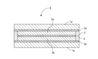
- FIG. 1 is a schematic cross-sectional view showing one embodiment of an EC element of the present invention.
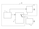
- FIG. 2 is a schematic diagram showing an example of a driving device including an EC element of the present invention.
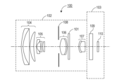
- 1 is a schematic diagram of an example of an imaging device in which an optical filter is disposed in a lens unit.
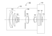
- 1 is a schematic diagram of an example of an imaging device in which an optical filter is disposed in the imaging device;
- FIG. 1 is a schematic view showing a window material using an EC element according to an embodiment of the present invention.
- FIG. 2 is a schematic cross-sectional view in the thickness direction of an overview showing a window material using an EC element according to the present embodiment.
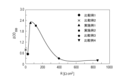
- 1 is a graph plotting the optical density change ⁇ OD 550 versus the ionic resistance R of each separator.
- 1 is a graph plotting the optical density change ⁇ OD 550 versus the tortuosity ⁇ for each separator.
- the electrochromic element of the present invention is an EC element having a pair of electrochromic layers sandwiched between them by a separator that divides the gap between the electrodes.
- the EC element of the present invention is a complementary EC element in which one of the pair of EC layers contains at least a cathodic electrochromic compound and the other contains at least an anodic electrochromic compound, and by specifying the ionic resistance of the separator, memory properties are imparted during coloring, thereby achieving low power consumption.
- excellent transparency is also obtained by limiting the average fiber diameter of the separator.
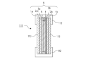
- FIG. 1 is a cross-sectional schematic diagram in the thickness direction showing the configuration of one embodiment of the EC element 6 of the present invention.
- 1a and 1b are a pair of substrates, and a pair of electrodes 2a and 2b are formed on one side of the substrates 1a and 1b on the inner side of the element.
- EC layers 3a and 3b are provided in contact with the electrodes 2a and 2b, respectively, and the EC layers 3a and 3b are partitioned by a separator 4.
- a seal 5 is provided on the outer periphery of the element so as to surround the EC layers 3a and 3b.
- the substrate 1a will be referred to as the first substrate, the substrate 1b as the second substrate, the electrode 2a as the first electrode, the electrode 2b as the second electrode, the EC layer 3a as the first EC layer, and the EC layer 3b as the second EC layer.
- the pair of substrates 1a, 1b are transparent substrates, and are required to be made of an electrical insulator such as glass or resin, which is highly transparent, has excellent heat resistance, and is also highly chemically stable.
- an electrical insulator such as glass or resin
- glass optical glass, quartz glass, white plate glass, blue plate glass, borosilicate glass, alkali-free glass, chemically strengthened glass, etc. can be used, and in particular, alkali-free glass is preferably used in terms of transparency and durability.
- resin polycarbonate (PC), acrylic (PMMA), polyethylene terephthalate (PET), transparent polyimide (PI), etc. can be used. Furthermore, it is preferable to use resins with a hard coat layer formed on the surface to improve scratch resistance.
- the pair of electrodes 2a, 2b are made of a transparent conductive material, such as indium tin oxide (ITO), fluorine-doped tin oxide (FTO), tin oxide (NESA), indium zinc oxide (IZO), graphene, etc.
- a transparent conductive material such as indium tin oxide (ITO), fluorine-doped tin oxide (FTO), tin oxide (NESA), indium zinc oxide (IZO), graphene, etc.
- conductive polymers whose conductivity has been improved by doping such as polyaniline, polypyrrole, polythiophene, polyacetylene, polyparaphenylene, and complexes of polyethylenedioxythiophene (PEDOT) and polystyrenesulfonic acid.
- the pair of EC layers 3a, 3b separated by the separator 4 is preferably a solution in which an EC compound is dissolved in an organic solvent, or a gel, and may contain an electrolyte.
- the pair may have a spacer that has the function of defining the distance between the first electrode 2a and the separator 4, and the distance between the second electrode 2b and the separator 4.
- the spacer may be made of an inorganic material such as silica beads or glass fiber, or an organic material such as polydivinylbenzene, polyimide, polytetrafluoroethylene, fluororubber, or epoxy resin.
- the EC layers 3a and 3b can be formed by injecting a liquid containing an EC compound prepared in advance into the gap between the pair of electrodes 2a and 2b and the separator 4 using a vacuum injection method, air injection method, meniscus method, etc., or by dropping a liquid containing an EC compound using the ODF method and then vacuum laminating it together with the separator 4, or by coating the pair of electrodes 2a and 2b using blade coating, bar coating, slit die coating, etc., and then laminating it together with the separator 4.
- the EC compound is preferably an organic compound
- the first EC layer 3a contains at least one cathodic electrochromic compound that changes color from a transparent state due to a reduction reaction
- the second EC layer 3b contains at least one anodic electrochromic compound that changes color from a transparent state due to an oxidation reaction.
- An element having both an anodic EC compound and a cathodic EC compound is called a complementary EC element, with the anodic EC compound also called the anode material and the cathodic compound also called the cathode material.
- the EC compound is colored at both of the pair of electrodes 2a, 2b, so that a large change in optical density is obtained when colored.
- Organic EC compounds include conductive polymers such as polythiophene and polyaniline, viologen compounds, anthraquinone compounds, oligothiophene derivatives, phenazine derivatives, and other organic low molecular weight compounds.
- the first EC layer 3a may contain one or more anodic EC compounds
- the second EC layer 3b may contain one or more cathodic EC compounds.
- the EC layers 3a and 3b may be made of the same composition containing one or more anodic EC compounds and one or more cathodic EC compounds.
- the difference in redox potential between the EC compounds is small.
- the anodic and cathodic compounds may be combined to have four or more types of EC compounds, or five or more types of EC compounds.
- the redox potential of the multiple anodic materials is preferably within 60 mV, and the redox potential of the multiple cathodic materials is preferably within 60 mV.
- the multiple EC compounds may include a compound having an absorption peak from 400 nm to 500 nm, a compound having an absorption peak from 500 nm to 650 nm, and a compound having an absorption peak above 650 nm.
- the absorption peak refers to a peak with a half-width of 20 nm or more.
- the material When absorbing light, the material may be in an oxidized state, a reduced state, or a neutral state.
- the electrolyte that may be contained in the EC layers 3a and 3b is not limited as long as it is an ion-dissociating salt and has good solubility in a solvent and high compatibility with a solid electrolyte. Among them, an electrolyte having electron donating properties is preferable. These electrolytes can also be called supporting electrolytes. Examples of the electrolyte include inorganic ion salts such as various alkali metal salts and alkaline earth metal salts, quaternary ammonium salts, and cyclic quaternary ammonium salts.
- alkali metal salts of Li , Na, and K such as LiClO4 , LiSCN, LiBF4 , LiAsF6 , LiCF3SO3 , LiPF6 , LiI, NaI , NaSCN, NaClO4 , NaBF4 , NaAsF6 , KSCN, and KCl, (CH3)4NBF4, (C2H5)4NBF4, (n-C4H9)4NBF4, (n-C4H9 ) 4NPF6 , ( C2H5 ) 4NBr , ( C2H5 ) 4NClO4 , and ( n - C4H9 ) 4NClO , ammonium salts such as quaternary ammonium salts of ammonium phosphate , etc. and cyclic quaternary ammonium salts.
- ammonium salts such as quaternary ammonium salts of ammonium phosphate , etc. and cyclic quaternary
- the solvent for dissolving the EC compound and electrolyte is not particularly limited as long as it can dissolve the EC compound and electrolyte, but it is preferable to use a solvent that has polarity.
- Specific examples include water and organic polar solvents such as methanol, ethanol, propylene carbonate, ethylene carbonate, dimethyl sulfoxide, dimethoxyethane, ⁇ -butyrolactone, ⁇ -valerolactone, sulfolane, dimethylformamide, dimethoxyethane, tetrahydrofuran, acetonitrile, propionitrile, 3-methoxypropionitrile, benzonitrile, dimethylacetamide, methylpyrrolidinone, and dioxolane.
- water and organic polar solvents such as methanol, ethanol, propylene carbonate, ethylene carbonate, dimethyl sulfoxide, dimethoxyethane, ⁇ -butyrolactone, ⁇ -valerol
- the EC layers 3a and 3b may further contain a polymer matrix, a gelling agent, and a cross-linking agent.
- the EC layers 3a and 3b may be made to gel (physical gel) from a highly viscous liquid by adding only a polymer, or may be made to gel (chemical gel) by adding a cross-linking agent to a polymer matrix.
- polymers include polyacrylonitrile, carboxymethylcellulose, pullulan-based polymers, polyvinyl chloride, polyethylene oxide, polypropylene oxide, polyurethane, polyacrylate, polymethacrylate, polyamide, polyacrylamide, polyester, polyvinylpyridine, Nafion (registered trademark), etc.
- the seal 5 is preferably made of a material that is chemically stable, impermeable to gases and liquids, and does not inhibit the redox reaction of the EC compound.
- examples include inorganic materials such as glass frit, and organic materials such as epoxy resin.
- the separator 4 is preferably made of nanofibers, and in order to ensure transparency in the visible light region, it is particularly preferable to use nanocellulose (cellulose nanofiber, hereafter sometimes referred to as "CNF") with a fiber diameter of 10 nm or less. Specifically, it is preferable that the light transmittance at a wavelength of 550 nm is 80% or more.
- CNF nanocellulose
- the separator 4 is a selectively permeable membrane that does not allow the EC compound to pass through but does allow the electrolyte ions to pass through. This prevents contact between the excited cathodic EC compound contained in the first EC layer 3a and the anodic EC compound contained in the second EC layer 3b, suppressing cross-reactions (side reactions) between the two. As a result, low power consumption of the EC element 6 can be achieved.
- the separator 4 can be defined by various physical property values, but can be preferably defined by direct physical property parameters related to the porous structure, such as ionic resistance, tortuosity, etc.
- the ionic resistance R can be evaluated by measuring the impedance in the thickness direction of the separator 4 impregnated with an electrolyte solution, and the tortuosity ⁇ is defined by the following formula [1] as the ratio of the effective path length to the thickness of the separator 4.
- the separator 4 suppresses cross-reaction between the excited anodic EC compound and the excited cathodic EC compound, but the resistance of the separator 4 limits the electrode reaction between the electrodes 2a and 2b.
- the ionic resistance R in the thickness direction of the separator 4 is 50 ⁇ cm 2 or more and 300 ⁇ cm 2 or less, the electrode reaction between the electrodes 2a and 2b becomes dominant over the cross-reaction between the excited anodic EC compound and the excited cathodic EC compound, and memory properties that efficiently maintain the colored state are obtained.
- the ionic resistance R is preferably 50 ⁇ cm 2 or more and 150 ⁇ cm 2 or less.
- TFSI tetrabutylammonium TFSI/propylene carbonate solution
- TFSI trisfluoromethanesulfonylimide
- the tortuosity ⁇ of the separator 4 is preferably 1.5 or more and 4.5 or less, and taking into consideration the responsiveness of the EC element 6, the tortuosity ⁇ is preferably 1.5 or more and 3.0 or less.
- the EC element according to this embodiment can be used in optical filters, lens units, imaging devices, window materials, and the like.
- the optical filter according to the present embodiment includes an EC element according to the present invention and an active element connected to the EC element.
- the active element drives the EC element and adjusts the amount of light passing through the EC element.
- Examples of the active element include a transistor.
- the transistor may have an oxide semiconductor such as InGaZnO in an active region.
- the optical filter according to this embodiment has a driving device connected to the EC element according to the present invention.
- FIG. 2 is a schematic diagram showing an example of a driving device 20 for an EC element and an EC element 6 driven by the driving device 20.
- the driving device 20 of the optical filter according to this embodiment has a driving power supply 8, a resistance switch 9, and a controller 7.
- the driving power supply 8 applies to the EC element a voltage necessary for the EC material contained in the EC layer to cause an electrochemical reaction. It is preferable that the driving voltage be a constant voltage. This is because when the EC material is composed of multiple types of materials, the absorption spectrum may change due to differences in the redox potential differences and molar absorption coefficients of the materials, so a constant voltage is preferable.
- the driving power supply 8 starts applying voltage or maintains the applied state according to a signal from the controller 7, and the constant voltage application state is maintained during the period in which the light transmittance of the EC element 6 is controlled.
- the controller 7 controls the transmittance of the EC element 6 in a manner suited to the element being used. Specifically, this can involve inputting predefined conditions to the EC element 6 for the desired transmittance setting, or comparing the transmittance setting with the transmittance of the EC element 6 and selecting and inputting conditions that match the setting. Parameters that can be changed include voltage, current, and duty ratio.
- the controller 7 can change the color density of the EC element 6 by changing the voltage, current, or duty ratio.
- Pulse width modulation can also be performed as follows.
- the resistance switch 9 switches between a resistor R1 (not shown) and a resistor R2 larger than the resistor R1, and connects them in series in a closed circuit including the drive power source 8 and the EC element 6.
- the resistance value of resistor R1 is preferably smaller than the largest impedance of the element closed circuit, and is preferably 10 ⁇ or less.
- the resistance value of resistor R2 is preferably larger than the largest impedance of the element closed circuit, and is preferably 1 M ⁇ or more.
- Resistor R2 may be air. In this case, strictly speaking the closed circuit becomes an open circuit, but it can be considered as a closed circuit by regarding the air as resistor R2.
- the controller 7 sends a switching signal to the resistor switch 9 to control the switching of resistors R1 and R2, but it is also possible to generate a PWM signal using a comparator or the like without using the resistor switch 9.
- the lens unit includes an imaging optical system having a plurality of lenses and an optical filter having the EC element of the present invention.
- the optical filter may be provided either between the plurality of lenses or outside the lens.
- the optical filter is preferably provided on the optical axis of the lens.
- the imaging device of this embodiment has an optical filter and a light receiving element that receives light that has passed through the optical filter.
- imaging devices include cameras, video cameras, and mobile phones with cameras.
- the imaging device may be in a form in which a main body having a light receiving element and a lens unit having a lens can be separated.
- the present invention also includes a form in which an optical filter separate from the imaging device is used during imaging.
- the position of the optical filter may be outside the lens unit, between the lens unit and the light receiving element, between multiple lenses (when the lens unit has multiple lenses), etc.
- FIG. 3A is a schematic diagram of an example of an imaging device in which an optical filter is disposed in a lens unit
- FIG. 3B is a schematic diagram of an example of an imaging device in which an optical filter is disposed in the imaging device.
- the imaging device 100 is an imaging device having a lens unit 102 and an imaging unit 103.
- the lens unit 102 has an optical filter 101 and an imaging optical system having a plurality of lenses or a lens group.
- the optical filter 101 is an optical filter having the EC element of the present invention in the above-described embodiment.
- Lens unit 102 for example, in FIG. 3A, represents a rear-focus zoom lens in which focusing is performed behind the aperture. It has four lens groups, in order from the object side: a first lens group 104 with positive refractive power, a second lens group 105 with negative refractive power, a third lens group 106 with positive refractive power, and a fourth lens group 107 with positive refractive power. Magnification is changed by changing the distance between second lens group 105 and third lens group 106, and focusing is performed by moving some of the lens groups in fourth lens group 107.
- the lens unit 102 for example, has an aperture stop 108 between the second lens group 105 and the third lens group 106, and also has an optical filter 101 between the third lens group 106 and the fourth lens group 107.
- the lens unit is arranged so that light passing through each of the lens groups 104 to 107, the aperture stop 108, and the optical filter 101 passes through, and the amount of light can be adjusted using the aperture stop 108 and the optical filter 101.
- the lens unit 102 is detachably connected to the imaging unit 103 via a mount member (not shown).
- the optical filter 101 is disposed between the third lens group 106 and the fourth lens group 107 in the lens unit 102, but the imaging device 100 is not limited to this configuration.
- the optical filter 101 may be disposed either in front of (on the subject side) or behind (on the imaging unit 103 side) the aperture stop 108, or in front of, behind, or between any of the first to fourth lens groups 104 to 107. Placing the optical filter 101 at a position where light converges has the advantage that the area of the optical filter 101 can be reduced.
- the configuration of the lens unit 102 is not limited to the above configuration, and can be selected as appropriate.
- the rear focus type it can be an inner focus type in which focusing is performed in front of the aperture, or other types.
- special lenses such as fisheye lenses and macro lenses can also be selected as appropriate.
- the imaging unit 103 has a glass block 109 and a light receiving element 110.
- the glass block 109 is a glass block such as a low-pass filter, face plate, or color filter.
- the light receiving element 110 is a sensor unit that receives light that has passed through the lens unit, and an imaging element such as a CCD or CMOS can be used. It may also be an optical sensor such as a photodiode, and any device that acquires and outputs information on the intensity or wavelength of light can be used as appropriate.
- the driving device may be disposed inside the lens unit 102 or outside the lens unit 102.
- the EC element 6 in the lens unit 102 is connected to the driving device through wiring to control the driving.
- the optical filter 101 is disposed inside the lens unit 102.
- the present invention is not limited to this configuration, and it is sufficient that the optical filter 101 is disposed at an appropriate location inside the imaging device 100, and the light receiving element 110 is disposed so as to receive light that has passed through the optical filter 101.
- the imaging unit 103 may have an optical filter 101.
- FIG. 3B is a diagram for explaining the configuration of another example of the imaging device of this embodiment, and is a schematic diagram of the configuration of an imaging device having an optical filter in the imaging unit 103.
- the optical filter 101 is disposed immediately before the light receiving element 110.
- the connected lens unit 102 itself does not need to have the optical filter 101, so it is possible to configure a dimmable imaging device using an existing lens unit 102.
- the imaging device 100 of this embodiment can be applied to products that have a combination of light intensity adjustment and a light receiving element.
- it can be used in cameras, digital cameras, video cameras, and digital video cameras, and can also be applied to products that have built-in imaging devices, such as mobile phones, smartphones, PCs, and tablets.
- the imaging device 100 of this embodiment by using the optical filter 101 as a dimming component, it is possible to appropriately adjust the dimming amount with a single filter, which has the advantages of reducing the number of components and saving space.
- the window material according to the present embodiment includes an EC element according to the present invention and an active element connected to the EC element.
- the active element drives the EC element and adjusts the amount of light passing through the EC element.
- the active element may be, for example, a transistor.
- the transistor may have an oxide semiconductor such as InGaZnO in an active region.
- the window material according to the present embodiment may also be called a variable transmittance window.
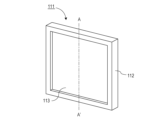
- FIG. 4A is an overview diagram showing a light control window as a window material using the EC element according to the present invention
- FIG. 4B is a schematic diagram showing a cross section in the thickness direction of the center part (X-X') of the light control window in FIG. 4A
- the light control window 111 of this embodiment is composed of an EC element (optical filter), transparent plates 113, 113 that sandwich it, and a frame 112 that surrounds and integrates the whole.
- the EC element has the configuration shown in FIG. 1 and has a drive unit (not shown), which may be integrated within the frame 112, or may be arranged outside the frame 112 and connected to the EC element 6 through wiring.
- the transparent plate 113 is not particularly limited as long as it is made of a material with high light transmittance, and is preferably made of a glass material considering its use as a window material.
- the material of the frame 112 is not important, but anything that covers at least a portion of the EC element 6 and has an integrated form may be considered as a frame.
- the EC element 6 is a component independent of the transparent plate 113, but for example, the substrates 1a and 1b of the EC element 6 may be considered as the transparent plates 113, 113.
- Such a light-control window can be used, for example, to adjust the amount of sunlight entering a room during the day. Since it can be used to adjust not only the amount of sunlight but also the amount of heat, it can be used to control the brightness and temperature inside a room. It can also be used as a shutter to block the view from outside into the room. In addition to glass windows for buildings, such light-control windows can also be used as window materials for vehicles such as cars, trains, airplanes, and ships.
- the EC element of the present invention can be used in optical filters, lens units, imaging devices, window materials, etc.
- EC mirrors may be installed in automobiles as anti-glare mirrors.
- EC mirrors can be constructed by having an electrochromic element and a reflective member inside or outside the EC element. Having a reflective member inside means that the electrodes of the EC element are reflective. Having a reflective member outside means that a reflective member is provided in contact with the electrodes of the EC element or via another transparent member.
- Table 1 shows the physical properties of the separators used in this example.
- the thickness of each separator is 20 ⁇ m, and the light transmittance is at a wavelength of 550 nm. It can be seen that No. 2 to No. 5, which have an average fiber diameter of 10 nm or less, have high transparency, and that even if the average fiber diameter is the same, there are differences in ionic resistance and tortuosity.
- Example 1 Separator No. 2 shown in Table 1 and an ITO glass substrate with a sheet resistance of 10 ⁇ / ⁇ were used to prepare an EC element by ODF and vacuum lamination.
- the layer thickness of the pair of EC layers was specified by kneading gap control particles with a diameter of 40 ⁇ m.
- Each EC layer contains the following anodic EC compound and cathodic EC compound, and propylene carbonate as a solvent, and is a chemical gel crosslinked with polyvinylpyridine polymer.
- the configuration of the pair of EC layers is the same.
- the light control area of the element was 20 mm x 20 mm, and the outer periphery was sealed with epoxy resin in a manner surrounding the outer periphery.
- Anodic EC Compound MOPOPhO1MedMdHPhzn: 3-(2-isoproxy-6-methoxyphenyl)-1,5,10-trimethyl-8-phenoxy-5,10-dihydrophenazine mMeOPhO1MediPrdHPhzn: 5,10-diisopropyl-2-(3-methoxyphenoxy)-7-methyl-5,10-dihydrophenazine
- pdtBuPh3MeVTFSI 1,1'-bis(4-tert-butyl)phenyl-3-methyl-4,4'-dipyridinium bis[bis(trifluoromethanesulfonyl)imide]
- the light transmittance at a wavelength of 550 nm dropped from 76.2% to 1.0% in 153 seconds.
- Example 2 An EC element was produced in the same manner as in Example 1, except that separator No. 3 shown in Table 1 was used.
- the light transmittance at a wavelength of 550 nm dropped from 80.4% to 1.0% in 166 seconds.
- Separator No. 1 had a large average fiber diameter of 3.2 ⁇ m, which not only scattered visible light and impaired the transparency of the EC element, but also had too low ionic resistance R to exhibit memory properties, requiring a large amount of power to maintain the colored state.
- Comparative Examples 2, 3, and 4 An EC element of Comparative Example 2 was prepared in the same manner as in Example 1, except that no separator was used. In addition, EC elements of Comparative Examples 3 and 4 were prepared in the same manner as in Example 1, except that separators Nos. 4 and 5 shown in Table 1 were used.
- FIG. 5 shows a graph plotting the optical density change ⁇ OD 550 at a wavelength of 550 nm when a constant voltage of 0.55 V is applied for 3 minutes for the obtained EC element and each of the EC elements of Examples 1, 2, and Comparative Example 1 with respect to the ionic resistance R of the separator.
- the ionic resistance R of the separator increases, the element current decreases, but nevertheless, the optical density change ⁇ OD 550 of the EC elements of Examples 1 and 2 is greater than that of Comparative Examples 1 and 2. This indicates that the electrode reaction is dominant over the charge exchange reaction (side reaction), and the colored state can be efficiently maintained.
- the optical density change ⁇ OD 550 is small because the electrode reaction is limited by the large ionic resistance R of the separator. Therefore, the ionic resistance R in the thickness direction of the separator is 50 ⁇ cm 2 or more and 300 ⁇ cm 2 or less.
- FIG. 6 shows a graph in which the optical density change ⁇ OD 550 at a wavelength of 550 nm when a constant voltage of 0.55 V was applied for 3 minutes for each of the EC elements of Examples 1 and 2 and Comparative Examples 1 to 4 is plotted against the tortuosity ⁇ of the separator. It can be seen that the tortuosity ⁇ of the separator is also preferably 1.5 or more and 4.5 or less.
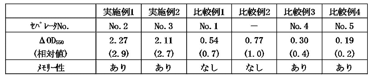
- Table 2 shows the optical density change ⁇ OD 550 at a wavelength of 550 nm when a constant voltage of 0.55 V is applied for 3 minutes and the presence or absence of memory properties for each of the EC elements of Examples 1 and 2 and Comparative Examples 1 to 4.
- the relative values in the column for optical density change ⁇ OD 550 are relative values with the value of optical density change ⁇ OD 550 of Comparative Example 2 taken as 1.0.
- the memory properties were evaluated by applying a constant voltage of 0.55 V to each EC element for 3 minutes, and then placing it in an open circuit state. If the absolute value of the optical density change ⁇ OD 550 (increase in transmittance) after 1 hour was less than 0.3, it was determined that the element had memory properties, and if it was 0.3 or more, it was determined that the element did not have memory properties.
Landscapes
- Physics & Mathematics (AREA)
- Nonlinear Science (AREA)
- General Physics & Mathematics (AREA)
- Optics & Photonics (AREA)
- Chemical & Material Sciences (AREA)
- Chemical Kinetics & Catalysis (AREA)
- Electrochromic Elements, Electrophoresis, Or Variable Reflection Or Absorption Elements (AREA)
Abstract
電極2a,2b間の間隙をセパレータ4で二分し、該セパレータ4を挟んで一対のEC層3a,3bを有するEC素子において、該セパレータ4として、0.1MテトラブチルアンモニウムTFSI/炭酸プロピレン溶液を含浸した時の厚み方向のイオン抵抗が50Ωcm2以上300Ωcm2以下であるセパレータを用いる。
Description
本発明は、エレクトロクロミック素子と、該エレクトロクロミック素子を用いて構成された機器に関する。
エレクトロクロミック(以下、「EC」と表記する場合がある)素子は、一対の電極と、その電極間に配置されたEC層と、を有する素子であり、一対の電極間に電圧を印加してEC層内の化合物を酸化若しくは還元することによって可視光領域の色相や光量を調整する能動的な光学素子である。
これまでにEC素子は住宅や航空機の調光窓として徐々に使用されてきたが、近年では環境配慮需要の高まりによって従来の素子性能を維持しながら更に大面積且つ低消費電力を実現する調光窓の開発が求められている。
有機EC化合物を用いたEC素子は、先ず光量調整範囲が広く色設計が比較的容易であるという特徴を有している。さらに、着色効率(光学濃度変化を必要電荷量で除した量)を考慮した場合、一対の電極間には電気化学的に活性なアノード性材料と電気化学的に活性なカソード性材料とを相補的に含み、それらの何れもがEC性を持つことが好ましい。また、高速応答を実現するためには、単位時間当たりにより多くの有機EC化合物が電極表面で反応する必要があり、そのためにEC層を溶液、若しくはゲルとして有機EC化合物をEC層内部で自由に移動できるような構成とすることが好ましい。しかしながら、このような構成を採用した場合、一対の電極で反応したアノード性、及びカソード性有機EC化合物は、EC層内部で電荷交換(副反応)を行い中性状態に緩和してしまう。従って、光学濃度を維持するのに継続して通電を行う必要があり、これが相補型有機EC素子の低消費電力化の妨げとなっていた。
特許文献1は、相補型有機EC素子において、電解質イオンを透過するが反応分子を透過しない選択透過膜をEC層中に設置することにより、一対の電極で生成した反応物間の副反応を回避する素子構造を開示している。
また、特許文献2は、相補型有機EC素子において、素子の光透過率が80%以上を実現する選択透過膜を用いて、一対の電極で生成した反応物間の副反応を回避する素子構造を開示している。
しかしながら、上記従来技術はEC層を二つの区画に分離する選択透過膜の要件、即ち透明性に関する要件と、副反応の発生を防いで消費電力低減を実現する要件が不明で、また特許文献2では消費電力低減の効果も十分とは言えなかった。
本発明は上記の問題点に鑑み、相補型有機EC素子において、一対の電極で生成した反応物間の副反応を回避すると共に素子にメモリー性を付与し、低消費電力を実現すること、さらには中性状態時の優れた透明性を付与することを目的とする。
本発明は、第一の電極と、第二の電極と、前記第一の電極と前記第二の電極間の間隙を二分するセパレータと、前記第一の電極と前記セパレータとの間に配置され、少なくとも一つカソード性エレクトロクロミック化合物を含む第一のエレクトロクロミック層と、前記第二の電極と前記セパレータとの間に配置され、少なくとも一つのアノード性エレクトロクロミック化合物を含む第二のエレクトロクロミック層と、を有するエレクトロクロミック素子であって、
0.1MテトラブチルアンモニウムTFSI/炭酸プロピレン溶液を含浸した時の前記セパレータの厚み方向のイオン抵抗が50Ωcm2以上300Ωcm2以下であることを特徴とする。
0.1MテトラブチルアンモニウムTFSI/炭酸プロピレン溶液を含浸した時の前記セパレータの厚み方向のイオン抵抗が50Ωcm2以上300Ωcm2以下であることを特徴とする。
本発明によれば、着色時のメモリー性が得られることから低消費電力が実現し、さらに、セパレータを平均繊維径を限定することで、中性時の透明性に優れたEC素子を実現することができる。
本発明のエレクトロクロミック素子は、電極間の間隙をセパレータで二分し、該セパレータを挟んで一対のエレクトロクロミック層を有したEC素子である。本発明のEC素子は、一対のEC層の一方が少なくともカソード性エレクトロクロミック化合物を、他方が少なくともアノード性エレクトロクロミック化合物を含む相補型EC素子であり、上記セパレータのイオン抵抗を特定することにより、着色時のメモリー性を付与して、低消費電力を図ったものである。本発明においては、セパレータの平均繊維径を限定することで、優れた透明性も得られる。
以下、図面を参照しながら本発明に係るEC素子の構成について、好適な実施の形態を例示的に詳しく説明する。但し、この実施の形態に記載されている構成、相対配置等は、特に記載がない限り、本発明の範囲を限定する趣旨のものではない。
〈EC素子〉
先ず、図1を用いて本発明のEC素子の構成について説明する。図1は本発明のEC素子6の一実施形態の構成を示した厚さ方向の断面模式図である。図1において、1a、1bは一対の基板で、基板1a、1bの素子内側の片面には、それぞれ一対の電極2a、2bが形成される。さらに、電極2a、2bに接してEC層3a、3bがそれぞれ設置され、EC層3a、3bはセパレータ4によって区画されている。また素子の外周部には、EC層3a、3bを囲繞する形でシール5が設置される。以下、便宜上、基板1aを第一の基板、基板1bを第二の基板、電極2aを第一の電極、電極2bを第二の電極、EC層3aを第一のEC層、EC層3bを第二のEC層と呼ぶ。
先ず、図1を用いて本発明のEC素子の構成について説明する。図1は本発明のEC素子6の一実施形態の構成を示した厚さ方向の断面模式図である。図1において、1a、1bは一対の基板で、基板1a、1bの素子内側の片面には、それぞれ一対の電極2a、2bが形成される。さらに、電極2a、2bに接してEC層3a、3bがそれぞれ設置され、EC層3a、3bはセパレータ4によって区画されている。また素子の外周部には、EC層3a、3bを囲繞する形でシール5が設置される。以下、便宜上、基板1aを第一の基板、基板1bを第二の基板、電極2aを第一の電極、電極2bを第二の電極、EC層3aを第一のEC層、EC層3bを第二のEC層と呼ぶ。
次に本発明のEC素子を構成する部材について詳細に説明する。
一対の基板1a,1bは透明基板であり、ガラスや樹脂等、電気絶縁体で透明性が高く、耐熱性に優れ化学的安定性も高いことが求められる。ガラスとしては、光学ガラス、石英ガラス、白板ガラス、青板ガラス、ホウケイ酸ガラス、無アルカリガラス、化学強化ガラス等を用いることができ、特に透明性や耐久性の点から無アルカリガラスを好適に使用することができる。樹脂としては、ポリカーボネート(PC)、アクリル(PMMA)、ポリエチレンテレフタレート(PET)、透明ポリイミド(PI)等を用いることができる。また、これら樹脂の表面には耐擦傷性を向上するためにハードコート層を形成したものを好適に使用することができる。
一対の電極2a、2bとしては、透明な導電材料が用いられ、例えば、酸化インジウムスズ合金(ITO)、フッ素ドープ酸化スズ(FTO)、酸化スズ(NESA)、酸化インジウム亜鉛(IZO)、グラフェン等を挙げることができる。また、ドーピング処理等で導電率を向上させた導電性ポリマー、例えば、ポリアニリン、ポリピロール、ポリチオフェン、ポリアセチレン、ポリパラフェニレン、ポリエチレンジオキシチオフェン(PEDOT)とポリスチレンスルホン酸の錯体等も好適に用いられる。
セパレータ4によって区画される一対のEC層3a、3bは、有機溶媒にEC化合物を溶解させた溶液、若しくはゲルであることが好ましく、電解質を含んでもよい。また、第一の電極2aとセパレータ4との距離、及び第二の電極2bとセパレータ4との距離を規定する機能を有するスペーサーを有してもよい。スペーサーは、シリカビーズ、ガラスファイバー等の無機材料や、ポリジビニルベンゼン、ポリイミド、ポリテトラフルオロエチレン、フッ素ゴム、エポキシ樹脂等の有機材料で構成されてもよい。
EC層3a、3bの形成方法は、一対の電極2a、2b、及びセパレータ4の間に設けた間隙に、真空注入法、大気注入法、メニスカス法等によって予め調製したEC化合物を含有する液体を注入する方法やODF法によりEC化合物を含有する液体を滴下した後にセパレータ4と共に真空貼合する方法や、一対の電極2a,2bにブレードコーティング、バーコーティング、スリットダイコーティング等によって塗工した後にセパレータ4と共に貼合する方法等が挙げられる。
EC化合物は有機化合物であることが好ましく、第一のEC層3aには還元反応によって透明状態から着色するカソード性エレクトロクロミック化合物が少なくとも一種、第二のEC層3bには酸化反応によって透明状態から着色するアノード性エレクトロクロミック化合物が少なくとも一種含まれる。アノード性EC化合物とカソード性EC化合物の双方を有する素子は相補型EC素子と呼ばれ、アノード性EC化合物はアノード材料、カソード性化合物はカソード材料とも呼ばれる。
相補型EC素子を駆動した場合、一方の電極では酸化反応によってEC化合物から電子が引き抜かれ、他方の電極では還元反応によってEC化合物が電子を受け取る。酸化反応によって中性分子からラジカルカチオンを生成してもよい。また、還元反応によって中性分子からラジカルアニオンを生成しても、ジカチオン分子からラジカルカチオンを生成してもよい。本発明においては、一対の電極2a,2bの双方においてEC化合物が着色するため、着色時に大きな光学濃度変化が得られる。
有機EC化合物は、ポリチオフェンやポリアニリン等の導電性高分子、ビオロゲン系化合物、アントラキノン系化合物、オリゴチオフェン誘導体、フェナジン誘導体等の有機低分子化合物等が挙げられる。
本発明においては、第一のEC層3aに一種以上のアノード性EC化合物が含まれていても良く、また、第二のEC層3bに一種以上のカソード性EC化合物が含まれていても良い。また、EC層3a,3bが一種以上のアノード性EC化合物と一種以上のカソード性EC化合物とを含む同じ組成物で構成されていても良い。
EC層3a,3bが複数種のEC化合物を含有する場合は、EC化合物の酸化還元電位の差が小さいことが好ましい。複数種のEC化合物を有する場合は、アノード性化合物とカソード性化合物とを合わせて4種以上、或いは5種以上のEC化合物を有してもよい。複数種のEC化合物を有する場合、複数のアノード材料の酸化還元電位は60mV以内が好ましく、複数のカソード材料の酸化還元電位は60mV以内が好ましい。複数種のEC化合物を有する場合、複数種のEC化合物は、400nm以上500nm以下に吸収ピークを有する化合物と、500nm以上650nm以下に吸収ピークを有する化合物と、650nm以上に吸収ピークを有する化合物を含んでいてもよい。吸収ピークは半値幅が20nm以上のものを指す。また、光を吸収する場合の材料の状態は酸化状態であっても、還元状態であっても、中性状態であってもよい。
EC層3a,3bが含んでいても良い電解質としては、イオン解離性の塩であり、且つ溶媒に対して良好な溶解性、固体電解質においては高い相溶性を示すものであれば限定されない。中でも電子供与性を有する電解質が好ましい。これら電解質は、支持電解質と呼ぶこともできる。電解質としては、例えば、各種のアルカリ金属塩、アルカリ土類金属塩等の無機イオン塩や4級アンモニウム塩や環状4級アンモニウム塩等が挙げられる。具体的にはLiClO4、LiSCN、LiBF4、LiAsF6、LiCF3SO3、LiPF6、LiI、NaI、NaSCN、NaClO4、NaBF4、NaAsF6、KSCN、KCl等のLi、Na、Kのアルカリ金属塩等や、(CH3)4NBF4、(C2H5)4NBF4、(n-C4H9)4NBF4、(n-C4H9)4NPF6、(C2H5)4NBr、(C2H5)4NClO4、(n-C4H9)4NClO4等の4級アンモニウム塩及び環状4級アンモニウム塩等が挙げられる。
EC化合物及び電解質を溶かす溶媒としては、EC化合物や電解質を溶解できるものであれば特に限定されないが、特に極性を有するものが好ましい。具体的には水や、メタノール、エタノール、プロピレンカーボネート、エチレンカーボネート、ジメチルスルホキシド、ジメトキシエタン、γ-ブチロラクトン、γ-バレロラクトン、スルホラン、ジメチルホルムアミド、ジメトキシエタン、テトラヒドロフラン、アセトニトリル、プロピオンニトリル、3-メトキシプロピオンニトリル、ベンゾニトリル、ジメチルアセトアミド、メチルピロリジノン、ジオキソラン等の有機極性溶媒が挙げられる。
EC層3a,3bは、さらにポリマーマトリックスやゲル化剤、架橋剤を含有してもよい。この場合、EC層3a,3bはポリマー単独の添加で高粘稠液体からゲル(物理ゲル)とする場合や、ポリマーマットリックスに更に架橋剤を添加することでゲル(化学ゲル)とする場合が挙げられる。ポリマーとしては、例えばポリアクリロニトリル、カルボキシメチルセルロース、プルラン系ポリマー、ポリ塩化ビニル、ポリエチレンオキサイド、ポリプロピレンオキサイド、ポリウレタン、ポリアクリレート、ポリメタクリレート、ポリアミド、ポリアクリルアミド、ポリエステル、ポリビニルピリジン、ナフィオン(登録商標)等が挙げられる。
シール5としては、化学的に安定で気体及び液体を透過させず、EC化合物の酸化還元反応を阻害しない材料であることが好ましい。例えば、ガラスフリット等の無機材料、エポキシ樹脂等の有機材料等が挙げられる。
セパレータ4は、ナノ繊維から構成されることが好ましく、可視光領域の透明性を担保するために、特に繊維径10nm以下のナノセルロース(セルロースナノファイバー、以下「CNF」と表記する場合がある)を好ましく用いることができる。具体的には、波長550nmにおける光透過性が80%以上であることが好ましい。
ここで、低消費電力を実現する本発明のEC素子のセパレータの要件について、詳細に説明する。
セパレータ4はEC化合物を透過しないが電解質イオンを透過する選択透過膜であり、これによって第一のEC層3aに含まれる励起状態のカソード性EC化合物と、第二のEC層3bに含まれるアノード性EC化合物間の接触が阻まれ、両者の交差反応(副反応)を抑制することができる。その結果、EC素子6の低消費電力化を実現できる。
セパレータ4は種々の物性値によって規定することができるが、多孔質構造に関わる直接的な物性パラメータとしてイオン抵抗、曲路率等によって好ましく規定することができる。イオン抵抗Rは電解質溶液を含浸したセパレータ4の厚み方向のインピーダンス測定によって評価することができ、また曲路率τはセパレータ4の厚さに対する実効的な経路長の比として下記式[1]によって定義される。
τ=l/d=((R・ε)/(ρ・d))1/2 [1]
l:セパレータ4の厚み方向の実効的な経路長(m)
d:セパレータ4の厚さ(m)
R:イオン抵抗(Ωcm2)
ε:気孔率
ρ:電解質溶液の抵抗率(Ω)
τ=l/d=((R・ε)/(ρ・d))1/2 [1]
l:セパレータ4の厚み方向の実効的な経路長(m)
d:セパレータ4の厚さ(m)
R:イオン抵抗(Ωcm2)
ε:気孔率
ρ:電解質溶液の抵抗率(Ω)
セパレータ4によって、励起状態のアノード性EC化合物と励起状態のカソード性EC化合物間の交差反応が抑制されるが、セパレータ4の抵抗によって、電極2a,2b間の電極反応は制限される。本発明においては、セパレータ4の厚み方向のイオン抵抗Rが50Ωcm2以上300Ωcm2以下であれば、電極2a,2b間の電極反応が、励起状態のアノード性EC化合物と励起状態のカソード性EC化合物間の交差反応よりも優勢となり、着色状態を効率よく維持するメモリー性が得られる。また、EC素子6の応答性を考慮すれば、イオン抵抗Rは50Ωcm2以上150Ωcm2以下が好ましい。イオン抵抗Rを測定する時の電解質溶液としては、0.1MテトラブチルアンモニウムTFSI/炭酸プロピレン溶液(TFSI:トリスフルオロメタンスルホニルイミド)を用いる。
また、イオン抵抗Rと同様の理由で、セパレータ4の曲路率τは1.5以上4.5以下が好ましく、EC素子6の応答性を考慮すれば、曲路率τは1.5以上3.0以下が好ましい。
〈EC素子の用途〉
本実施形態に係るEC素子は、光学フィルタ、レンズユニット、撮像装置、窓材等に用いることができる。
本実施形態に係るEC素子は、光学フィルタ、レンズユニット、撮像装置、窓材等に用いることができる。
〔光学フィルタ〕
本実施形態に係る光学フィルタは、本発明に係るEC素子と、該EC素子に接続されている能動素子と、を有する。能動素子は、EC素子を駆動し、EC素子を通過する光の光量を調整する能動素子である。能動素子は、例えば、トランジスタ等が挙げられる。トランジスタは活性領域に、InGaZnOなどの酸化物半導体を有してもよい。
本実施形態に係る光学フィルタは、本発明に係るEC素子と、該EC素子に接続されている能動素子と、を有する。能動素子は、EC素子を駆動し、EC素子を通過する光の光量を調整する能動素子である。能動素子は、例えば、トランジスタ等が挙げられる。トランジスタは活性領域に、InGaZnOなどの酸化物半導体を有してもよい。
本実施形態に係る光学フィルタは、本発明に係るEC素子に接続されている駆動装置を有している。図2は、EC素子の駆動装置20と、駆動装置20が駆動するEC素子6の一例を示す模式図である。本実施形態に係る光学フィルタの駆動装置20は、駆動電源8、抵抗切替器9、及び制御器7を有する。
駆動電源8は、EC層に含まれるEC材料が電気化学反応を生じるのに必要な電圧をEC素子に印加する。駆動電圧は一定電圧であることがより好ましい。これは、EC材料が複数種類の材料で構成される場合は、材料の酸化還元電位差やモル吸光係数の差に起因して吸収スペクトルが変化する場合があるため、一定電圧であることが好ましいからである。駆動電源8の電圧印加開始或いは印加状態の保持は制御器7の信号で行われ、EC素子6の光透過率を制御する期間においては、一定電圧の印加状態が保持されている。
制御器7によるEC素子6の透過率の制御方法は、用いられる素子に適した方法が採用される。具体的には、所望の透過率の設定値に対して、予め規定されている条件をEC素子6に入力する方法や、透過率の設定値とEC素子6の透過率を比較して、設定値に合うように条件を選択して入力する方法が挙げられる。変化させるパラメータとしては、電圧、電流、デューティー比を挙げることができる。制御器7は、電圧、電流又はデューティー比を変化させることで、EC素子6の着色濃度を変化させることができる。
本実施形態において、電圧の変更、電流の変更、パルス幅の変調は、公知の手段を用いることができる。またパルス幅の変調は、以下のように行うこともできる。
抵抗切替器9は、駆動電源8とEC素子6を含む閉回路中に、不図示の抵抗R1と該抵抗R1よりも大きな抵抗R2とを切り替えて直列に接続するものである。抵抗R1の抵抗値としては、少なくとも素子閉回路の最も大きなインピーダンスよりも小さいことが好ましく、好ましくは10Ω以下である。抵抗R2の抵抗値としては、素子閉回路の最も大きなインピーダンスよりも大きいことが好ましく、好ましくは1MΩ以上である。尚、抵抗R2は空気であっても良い。この場合、厳密には閉回路は開回路となるが、空気を抵抗R2と見なすことで閉回路と考えることができる。
制御器7は、抵抗切替器9に切替信号を送り、抵抗R1と抵抗R2のスイッチングを制御するが、抵抗切替器9を有さずに、コンパレーター等を用いて、PWM信号を生成してもよい。
〔レンズユニット〕
本実施形態に係るレンズユニットは、複数のレンズを有する撮像光学系と、本発明のEC素子を有する光学フィルタとを有している。光学フィルタは、複数のレンズの間又はレンズの外側のいずれに設けられていてもよい。光学フィルタは、レンズの光軸上に設けられることが好ましい。
本実施形態に係るレンズユニットは、複数のレンズを有する撮像光学系と、本発明のEC素子を有する光学フィルタとを有している。光学フィルタは、複数のレンズの間又はレンズの外側のいずれに設けられていてもよい。光学フィルタは、レンズの光軸上に設けられることが好ましい。
〔撮像装置〕
本実施形態の撮像装置は、光学フィルタと、この光学フィルタを通過した光を受光する受光素子と、を有する。撮像装置とは、具体的には、カメラ、ビデオカメラ、カメラ付き携帯電話等が挙げられる。撮像装置は、受光素子を有する本体と、レンズを有するレンズユニットとが分離できる形態であってもよい。ここで撮像装置が、本体と、レンズユニットとで分離できる場合は、撮像時に撮像装置とは別体の光学フィルタを用いる形態も本発明に含まれる。尚、係る場合、光学フィルタの配置位置としては、レンズユニットの外側、レンズユニットと受光素子との間、複数あるレンズの間(レンズユニットが複数のレンズを有する場合)等が挙げられる。
本実施形態の撮像装置は、光学フィルタと、この光学フィルタを通過した光を受光する受光素子と、を有する。撮像装置とは、具体的には、カメラ、ビデオカメラ、カメラ付き携帯電話等が挙げられる。撮像装置は、受光素子を有する本体と、レンズを有するレンズユニットとが分離できる形態であってもよい。ここで撮像装置が、本体と、レンズユニットとで分離できる場合は、撮像時に撮像装置とは別体の光学フィルタを用いる形態も本発明に含まれる。尚、係る場合、光学フィルタの配置位置としては、レンズユニットの外側、レンズユニットと受光素子との間、複数あるレンズの間(レンズユニットが複数のレンズを有する場合)等が挙げられる。
図3Aは光学フィルタがレンズユニットに配置されている撮像装置の一例の模式図であり、図3Bは光学フィルタが撮像装置に配置されている撮像装置の一例の模式図である。
撮像装置100は、レンズユニット102と、撮像ユニット103と、を有する撮像装置である。レンズユニット102は、光学フィルタ101と、複数のレンズ又はレンズ群を有する撮像光学系と、を有する。光学フィルタ101は、上述の本実施形態の、本発明のEC素子を有する光学フィルタである。
レンズユニット102は、例えば、図3Aにおいて、絞りより後でフォーカシングを行うリアフォーカス式のズームレンズを表している。物体側より順に正の屈折力の第1のレンズ群104、負の屈折力の第2のレンズ群105、正の屈折力の第3のレンズ群106、正の屈折力の第4のレンズ群107の4つのレンズ群を有する。第2のレンズ群105と第3のレンズ群106の間隔を変化させて変倍を行い、第4のレンズ群107の一部のレンズ群を移動させてフォーカスを行う。
レンズユニット102は、例えば、第2のレンズ群105と第3のレンズ群106との間に開口絞り108を有し、また、第3のレンズ群106と第4のレンズ群107との間に光学フィルタ101を有する。レンズユニットを通過する光は、各レンズ群104乃至107、絞り108及び光学フィルタ101を通過するよう配置されており、開口絞り108及び光学フィルタ101を用いた光量の調整を行うことができる。レンズユニット102は、マウント部材(不図示)を介して撮像ユニット103に着脱可能に接続されている。
尚、本実施形態では、レンズユニット102内の第3のレンズ群106と第4のレンズ群107との間に光学フィルタ101が配置されているが、撮像装置100はこの構成に限定されない。例えば、光学フィルタ101は、開口絞り108の前(被写体側)或いは後(撮像ユニット103側)のいずれにあってもよく、また、第1乃至第4のレンズ群104乃至107のいずれの前、後、レンズ群の間にあってもよい。尚、光学フィルタ101を光の収束する位置に配置すれば、光学フィルタ101の面積を小さくできるなどの利点がある。
また、レンズユニット102の構成も上述の構成に限定されず、適宜選択可能である。例えば、リアフォーカス式の他、絞りより前でフォーカシングを行うインナーフォーカス式であっても良く、その他方式であっても構わない。また、ズームレンズ以外にも魚眼レンズやマクロレンズなどの特殊レンズも適宜選択可能である。
撮像ユニット103は、ガラスブロック109と、受光素子110と、を有する。ガラスブロック109は、ローパスフィルタやフェースプレートや色フィルタ等のガラスブロックである。また、受光素子110は、レンズユニットを通過した光を受光するセンサ部であって、CCDやCMOS等の撮像素子が使用できる。また、フォトダイオードのような光センサであっても良く、光の強度或いは波長の情報を取得し出力するものを適宜利用可能である。
図3Aのように、光学フィルタ101がレンズユニット102に組み込まれている場合、駆動装置はレンズユニット102内に配置されてもよく、レンズユニット102外に配置されてもよい。レンズユニット102外に配置される場合は、配線を通してレンズユニット102の内のEC素子6と駆動装置を接続し、駆動制御する。
また、上述の撮像装置100の構成では、光学フィルタ101がレンズユニット102の内部に配置されている。しかし、本発明はこの形態に限らず、光学フィルタ101は、撮像装置100内部の適当な箇所に配置され、受光素子110は光学フィルタ101を通過した光を受光するよう配置されていればよい。
例えば、図3Bに示したように、撮像ユニット103が光学フィルタ101を有していてもよい。図3Bは、本実施形態の撮像装置の別の一例の構成を説明する図であり、光学フィルタを撮像ユニット103に有する撮像装置の構成の模式図である。図3Bにおいては、例えば光学フィルタ101は受光素子110の直前に配置されている。撮像装置自体が光学フィルタ101を内蔵する場合、接続されるレンズユニット102自体が光学フィルタ101を持たなくてもよいため、既存のレンズユニット102を用いた調光可能な撮像装置を構成することが可能となる。
本実施形態の撮像装置100は、光量調整と受光素子の組合せを有する製品に適用可能である。例えばカメラ、デジタルカメラ、ビデオカメラ、デジタルビデオカメラに使用可能であり、また、携帯電話やスマートフォン、PC、タブレットなど撮像装置を内蔵する製品にも適用できる。
本実施形態の撮像装置100によれば、光学フィルタ101を調光部材として用いることにより、調光量を一つのフィルタで適宜可変させることが可能となり、部材点数の削減や省スペース化といった利点がある。
〔窓材〕
本実施形態に係る窓材は、本発明に係るEC素子と、該EC素子に接続されている能動素子を有する。能動素子は、EC素子を駆動し、EC素子を通過する光の光量を調整する能動素子である。能動素子は、例えば、トランジスタ等が挙げられる。トランジスタは活性領域に、InGaZnOなどの酸化物半導体を有していてもよい。本実施形態に係る窓材は、透過率可変窓と呼ぶこともできる。
本実施形態に係る窓材は、本発明に係るEC素子と、該EC素子に接続されている能動素子を有する。能動素子は、EC素子を駆動し、EC素子を通過する光の光量を調整する能動素子である。能動素子は、例えば、トランジスタ等が挙げられる。トランジスタは活性領域に、InGaZnOなどの酸化物半導体を有していてもよい。本実施形態に係る窓材は、透過率可変窓と呼ぶこともできる。
図4Aは本発明に係るEC素子を用いた窓材としての調光窓を示す概観図であり、図4Bは図4Aの調光窓の中央部(X-X’)の厚さ方向の断面図を示す模式図である。本実施形態の調光窓111は、EC素子(光学フィルタ)と、それを挟持する透明板113,113と、全体を囲繞して一体化するフレーム112とからなる。EC素子は図1に示した構成を備え、不示図の駆動装置を有しており、駆動装置はフレーム112内に一体化されていても良く、フレーム112外に配置され配線を通してEC素子6と接続されても良い。
透明板113は光透過率が高い材料であれば特に限定されず、窓材としての利用を考慮すればガラス素材であることが好ましい。フレーム112の材質は問わないが、EC素子6の少なくとも一部を被覆し、一体化された形態を有するもの全般をフレームとして見なして構わない。図4A、図4BにおいてEC素子6は透明板113とは独立した構成部材であるが、例えば、EC素子6の基板1a,1bを透明板113、113と見なしても構わない。
係る調光窓は、例えば日中の太陽光の室内への入射量を調整する用途に適用できる。太陽の光量の他、熱量の調整にも適用できるため、室内の明るさや温度の制御に使用することが可能である。また、シャッターとして、室外から室内への眺望を遮断する用途にも適用可能である。このような調光窓は、建造物用のガラス窓の他に、自動車や電車、飛行機、船など乗り物の窓材にも適用可能である。
このように、本発明のEC素子は、光学フィルタ、レンズユニット、撮像装置、窓材等に用いることができる。
また、EC素子の一方の光の経路に反射部材を設けることで、エレクトロクロミックミラーとすることもできる。ECミラーは、防眩ミラーとして、自動車に設けられてよい。ECミラーは、エレクトロクロミック素子と、EC素子の内部又は外部に反射部材とを有することで構成することができる。内部に反射部材を有するとは、EC素子の電極が反射性であることを示す。外部に反射部材を有するとは、EC素子の電極に接して又は他の透明部材を介して、反射部材が設けられていることを示す。
表1に、本実施例で用いたセパレータの物性値を示す。尚、セパレータの厚さはいずれも20μmで、光透過率は波長550nmの値である。平均繊維径が10nm以下であるNo.2乃至No.5については高い透明性を持っていること、また平均繊維径が同じであってもイオン抵抗や曲路率に差があることが分かる。

(実施例1)
表1に示したセパレータNo.2とシート抵抗が10Ω/□のITOガラス基板を用い、ODF・真空貼合によってEC素子を作製した。一対のEC層は直径40μmのギャップ制御粒子を混練することによって層厚を規定した。各EC層は、下記アノード性EC化合物及びカソード性EC化合物、及び溶媒としての炭酸プロピレンを含み、ポリビニルピリジンポリマーを架橋させた化学ゲルとしている。一対のEC層の構成は同じである。また、素子の調光領域は20mm×20mmとし、外周を囲繞する形でエポキシ樹脂にてシールを行った。
表1に示したセパレータNo.2とシート抵抗が10Ω/□のITOガラス基板を用い、ODF・真空貼合によってEC素子を作製した。一対のEC層は直径40μmのギャップ制御粒子を混練することによって層厚を規定した。各EC層は、下記アノード性EC化合物及びカソード性EC化合物、及び溶媒としての炭酸プロピレンを含み、ポリビニルピリジンポリマーを架橋させた化学ゲルとしている。一対のEC層の構成は同じである。また、素子の調光領域は20mm×20mmとし、外周を囲繞する形でエポキシ樹脂にてシールを行った。
アノード性EC化合物:
MOPOPhO1MedMdHPhzn:3-(2-イソプロキシ-6-メトキシフェニル)-1,5,10-トリメチル-8-フェノキシ-5,10-ジヒドロフェナジン
mMeOPhO1MediPrdHPhzn:5,10-ジイソプピル-2-(3-メトキシフェノキシ)-7-メチル-5,10-ジヒドロフェナジン
MOPOPhO1MedMdHPhzn:3-(2-イソプロキシ-6-メトキシフェニル)-1,5,10-トリメチル-8-フェノキシ-5,10-ジヒドロフェナジン
mMeOPhO1MediPrdHPhzn:5,10-ジイソプピル-2-(3-メトキシフェノキシ)-7-メチル-5,10-ジヒドロフェナジン
カソード性EC化合物:
F3BuAFlu2TFSI:9,9-ジメチル-2,7-ビス(4,4,4-トリフルオロブチル)-9H-シクロペンタ[1,2-c:4,3-c’]ジピリジニウムビス[ビス(トリフルオロメタンスルホニル)イミド]
pdtBuPh3MeVTFSI:1,1’-ビス(4-tert-ブチル)フェニル-3-メチル-4,4’-ジピリジニウムビス[ビス(トリフルオロメタンスルホニル)イミド]
F3BuAFlu2TFSI:9,9-ジメチル-2,7-ビス(4,4,4-トリフルオロブチル)-9H-シクロペンタ[1,2-c:4,3-c’]ジピリジニウムビス[ビス(トリフルオロメタンスルホニル)イミド]
pdtBuPh3MeVTFSI:1,1’-ビス(4-tert-ブチル)フェニル-3-メチル-4,4’-ジピリジニウムビス[ビス(トリフルオロメタンスルホニル)イミド]
上記4種のEC化合物は下記の濃度でEC層に含有させた。
MOPOPhO1MedMdHPhzn:27mM
mMeOPhO1MediPrdHPhzn:351mM
F3BuAFlu2TFSI:284mM
pdtBuPh3MeVTFSI:94mM
MOPOPhO1MedMdHPhzn:27mM
mMeOPhO1MediPrdHPhzn:351mM
F3BuAFlu2TFSI:284mM
pdtBuPh3MeVTFSI:94mM
得られたEC素子に一定電圧0.55Vを印加したところ、153秒で波長550nmの光透過率が76.2%から1.0%まで低下した。さらに電圧を180秒印加して光透過率が0.70%となった時点で開回路にしたところ、1時間後の光透過率は1.34%(光学濃度変化ΔOD550=-0.28)で着色状態を変わらず維持していた(メモリー性あり)。
(実施例2)
表1に示したセパレータNo.3を用いる以外は実施例1と同様にしてEC素子を作製した。得られたEC素子に一定電圧0.55Vを印加したところ、166秒で波長550nmの光透過率が80.4%から1.0%まで低下した。さらに電圧を180秒印加して光透過率が0.81%となった時点で開回路にしたところ、1時間後の光透過率は1.21%(光学濃度変化ΔOD550=-0.17)で着色状態を変わらず維持していた(メモリー性あり)。
表1に示したセパレータNo.3を用いる以外は実施例1と同様にしてEC素子を作製した。得られたEC素子に一定電圧0.55Vを印加したところ、166秒で波長550nmの光透過率が80.4%から1.0%まで低下した。さらに電圧を180秒印加して光透過率が0.81%となった時点で開回路にしたところ、1時間後の光透過率は1.21%(光学濃度変化ΔOD550=-0.17)で着色状態を変わらず維持していた(メモリー性あり)。
(比較例1)
表1に示したセパレータNo.1を用いる以外は実施例1と同様にしてEC素子を作製した。得られた素子に一定電圧0.55Vを印加したところ、60秒程度で電流が略一定となり、波長550nmの光透過率が18.2%から5.4%まで低下した。さらに電圧を180秒印加して光透過率が4.6%となった時点で開回路にしたところ、約90秒で初期の透過率まで回復した(光学濃度変化ΔOD550=-0.60(メモリー性なし)。
表1に示したセパレータNo.1を用いる以外は実施例1と同様にしてEC素子を作製した。得られた素子に一定電圧0.55Vを印加したところ、60秒程度で電流が略一定となり、波長550nmの光透過率が18.2%から5.4%まで低下した。さらに電圧を180秒印加して光透過率が4.6%となった時点で開回路にしたところ、約90秒で初期の透過率まで回復した(光学濃度変化ΔOD550=-0.60(メモリー性なし)。
セパレータNo.1は、平均繊維径が3.2μmと大きく、可視光を散乱してEC素子としての透明性を損なうばかりか、イオン抵抗Rも低すぎるためメモリー性を発現することがなく、着色状態を維持するのに大きな電力が必要であった。
(比較例2,3,4)
セパレータを用いない以外は実施例1と同様にして比較例2のEC素子を作製した。また、表1に示したセパレータNo.4,5を用いる以外は実施例1と同様にして比較例3,4のEC素子を作製した。
セパレータを用いない以外は実施例1と同様にして比較例2のEC素子を作製した。また、表1に示したセパレータNo.4,5を用いる以外は実施例1と同様にして比較例3,4のEC素子を作製した。
得られたEC素子と、実施例1,2及び比較例1の各EC素子について、一定電圧0.55Vを3分間印加した時の波長550nmの光学濃度変化ΔOD550を、セパレータのイオン抵抗Rに関してプロットしたグラフを図5に示す。セパレータのイオン抵抗Rが大きくなるにつれて素子電流は小さくなるが、それにも関わらず、実施例1,2のEC素子は光学濃度変化ΔOD550が比較例1や2よりも増大している。これは、電極反応が電荷交換反応(副反応)よりも優勢で、着色状態を効率よく維持できていることを示している。また、比較例3,4のEC素子では、セパレータのイオン抵抗Rが大きいことによって、電極反応が制限されることから、光学濃度変化ΔOD550が小さくなっていると考えられる。よって、セパレータの厚み方向のイオン抵抗Rは、50Ωcm2以上300Ωcm2以下である。
また、実施例1,2及び比較例1乃至4の各EC素子について、一定電圧0.55Vを3分間印加した時の波長550nmの光学濃度変化ΔOD550を、セパレータの曲路率τに関してプロットしたグラフを図6に示す。セパレータの曲路率τについても、1.5以上4.5以下が好ましいことがわかる。
表2に、実施例1,2及び比較例1乃至4の各EC素子について、一定電圧0.55Vを3分間印加した時の波長550nmの光学濃度変化ΔOD550と、メモリー性の有無を示す。光学濃度変化ΔOD550の欄の相対値は、比較例2の光学濃度変化ΔOD550の値を1.0とした相対値である。メモリー性は、各EC素子に一定電圧0.55Vを3分間印加した後に開回路状態とし、1時間後の光学濃度変化ΔOD550(透過率上昇)の絶対値が0.3未満であればメモリー性あり、0.3以上をメモリー性なしと判断した。
本発明は上記実施の形態に制限されるものではなく、本発明の精神及び範囲から離脱することなく、様々な変更及び変形が可能である。従って、本発明の範囲を公にするために以下の請求項を添付する。
本願は、2023年3月29日提出の日本国特許出願特願2023-053344を基礎として優先権を主張するものであり、その記載内容の全てをここに援用する。
2a,2b 電極
3a,3b エレクトロクロミック層
4 セパレータ
6 エレクトロクロミック素子
101 光学フィルタ
102 レンズユニット
110 受光素子
100 撮像装置
3a,3b エレクトロクロミック層
4 セパレータ
6 エレクトロクロミック素子
101 光学フィルタ
102 レンズユニット
110 受光素子
100 撮像装置
Claims (11)
- 第一の電極と、第二の電極と、前記第一の電極と前記第二の電極間の間隙を二分するセパレータと、前記第一の電極と前記セパレータとの間に配置され、少なくとも一種のカソード性エレクトロクロミック化合物を含む第一のエレクトロクロミック層と、前記第二の電極と前記セパレータとの間に配置され、少なくとも一種のアノード性エレクトロクロミック化合物を含む第二のエレクトロクロミック層と、を有するエレクトロクロミック素子であって、
0.1MテトラブチルアンモニウムTFSI/炭酸プロピレン溶液を含浸した時の前記セパレータの厚み方向のイオン抵抗が50Ωcm2以上300Ωcm2以下であることを特徴とするエレクトロクロミック素子。 - 前記セパレータはナノ繊維からなることを特徴とする請求項1に記載のエレクトロクロミック素子。
- 前記セパレータの平均繊維径が10nm以下であることを特徴とする請求項2に記載のエレクトロクロミック素子。
- 前記ナノ繊維はナノセルロースからなることを特徴とする請求項2に記載のエレクトロクロミック素子。
- 前記セパレータは曲路率が1.5以上4.5以下であることを特徴とする請求項1に記載のエレクトロクロミック素子。
- 前記セパレータは波長550nmの光透過率が80%以上であることを特徴とする請求項1に記載のエレクトロクロミック素子。
- 請求項1乃至6のいずれか一項に記載のエレクトロクロミック素子と、前記エレクトロクロミック素子に接続されているトランジスタと、を有することを特徴とする光学フィルタ。
- 請求項7に記載の光学フィルタと、複数のレンズを有する撮像光学系と、を有することを特徴とするレンズユニット。
- 請求項7に記載の光学フィルタと、前記光学フィルタを通過した光を受光する受光素子と、を有することを特徴とする撮像装置。
- 請求項1乃至6のいずれか一項に記載のエレクトロクロミック素子と、前記エレクトロクロミック素子に接続されているトランジスタと、を有することを特徴とする窓材。
- 請求項1乃至6のいずれか一項に記載のエレクトロクロミック素子と、前記エレクトロクロミック素子の内部又は外部に配置される反射部材と、を有することを特徴とするエレクトロクロミックミラー。
Priority Applications (1)
| Application Number | Priority Date | Filing Date | Title |
|---|---|---|---|
| US19/325,295 US20260010046A1 (en) | 2023-03-29 | 2025-09-10 | Electrochromic element and devices including the same |
Applications Claiming Priority (2)
| Application Number | Priority Date | Filing Date | Title |
|---|---|---|---|
| JP2023-053344 | 2023-03-29 | ||
| JP2023053344A JP2024141604A (ja) | 2023-03-29 | 2023-03-29 | エレクトロクロミック素子及びこれを用いた機器 |
Related Child Applications (1)
| Application Number | Title | Priority Date | Filing Date |
|---|---|---|---|
| US19/325,295 Continuation US20260010046A1 (en) | 2023-03-29 | 2025-09-10 | Electrochromic element and devices including the same |
Publications (1)
| Publication Number | Publication Date |
|---|---|
| WO2024203202A1 true WO2024203202A1 (ja) | 2024-10-03 |
Family
ID=92904450
Family Applications (1)
| Application Number | Title | Priority Date | Filing Date |
|---|---|---|---|
| PCT/JP2024/009261 Ceased WO2024203202A1 (ja) | 2023-03-29 | 2024-03-11 | エレクトロクロミック素子及びこれを用いた機器 |
Country Status (3)
| Country | Link |
|---|---|
| US (1) | US20260010046A1 (ja) |
| JP (1) | JP2024141604A (ja) |
| WO (1) | WO2024203202A1 (ja) |
Citations (5)
| Publication number | Priority date | Publication date | Assignee | Title |
|---|---|---|---|---|
| JPH09309173A (ja) * | 1996-03-21 | 1997-12-02 | Showa Denko Kk | イオン伝導性積層物、その製造方法及び用途 |
| US20180373107A1 (en) * | 2017-06-23 | 2018-12-27 | Essilor International | Electrochromic device with selective membrane |
| CN110055680A (zh) * | 2019-05-10 | 2019-07-26 | 上海纳旭实业有限公司 | 纳米纤维素复合膜的制备方法及产品和应用 |
| JP2019530128A (ja) * | 2016-07-13 | 2019-10-17 | アンスティテュ・ポリテクニック・ドゥ・グルノーブル | 電気化学発電装置用のイオン伝導性材料及び製造方法 |
| JP2022099249A (ja) * | 2020-12-22 | 2022-07-04 | キヤノン株式会社 | エレクトロクロミック素子、及びそれを有する光学フィルタ、レンズユニット、撮像装置、窓材、エレクトロクロミックミラー |
-
2023
- 2023-03-29 JP JP2023053344A patent/JP2024141604A/ja active Pending
-
2024
- 2024-03-11 WO PCT/JP2024/009261 patent/WO2024203202A1/ja not_active Ceased
-
2025
- 2025-09-10 US US19/325,295 patent/US20260010046A1/en active Pending
Patent Citations (5)
| Publication number | Priority date | Publication date | Assignee | Title |
|---|---|---|---|---|
| JPH09309173A (ja) * | 1996-03-21 | 1997-12-02 | Showa Denko Kk | イオン伝導性積層物、その製造方法及び用途 |
| JP2019530128A (ja) * | 2016-07-13 | 2019-10-17 | アンスティテュ・ポリテクニック・ドゥ・グルノーブル | 電気化学発電装置用のイオン伝導性材料及び製造方法 |
| US20180373107A1 (en) * | 2017-06-23 | 2018-12-27 | Essilor International | Electrochromic device with selective membrane |
| CN110055680A (zh) * | 2019-05-10 | 2019-07-26 | 上海纳旭实业有限公司 | 纳米纤维素复合膜的制备方法及产品和应用 |
| JP2022099249A (ja) * | 2020-12-22 | 2022-07-04 | キヤノン株式会社 | エレクトロクロミック素子、及びそれを有する光学フィルタ、レンズユニット、撮像装置、窓材、エレクトロクロミックミラー |
Also Published As
| Publication number | Publication date |
|---|---|
| JP2024141604A (ja) | 2024-10-10 |
| US20260010046A1 (en) | 2026-01-08 |
Similar Documents
| Publication | Publication Date | Title |
|---|---|---|
| CN107850814B (zh) | 电致变色元件、光学滤光器、透镜单元、成像装置和窗构件 | |
| US20160306251A1 (en) | Driving device for electrochromic device, electrochromic apparatus, optical filter, imaging apparatus, lens unit, and window member including electrochromic device, and method for driving electrochromic device | |
| JP6727755B2 (ja) | エレクトロクロミック装置、光学フィルタ、撮像装置、レンズユニットおよび窓材、エレクトロクロミック装置の駆動方法 | |
| JP2016038583A (ja) | エレクトロクロミック素子の駆動装置及び駆動方法 | |
| WO2016167163A1 (en) | Electrochromic element | |
| US9946137B2 (en) | Electrochromic element, lens unit, imaging device, and window member | |
| WO2017010360A1 (en) | Electrochromic element, optical filter, lens unit, imaging apparatus, and window member | |
| JP2020016805A (ja) | エレクトロクロミック装置とその駆動方法、レンズユニット、撮像装置、窓材 | |
| JP7463072B2 (ja) | エレクトロクロミック素子、レンズユニット、撮像装置及び調光窓 | |
| JP6884512B2 (ja) | エレクトロクロミック素子、光学フィルタ、レンズユニット、撮像装置及び窓材 | |
| US11047171B2 (en) | Electrochromic device, and lens unit, imaging apparatus and window including the electrochromic device | |
| WO2024203202A1 (ja) | エレクトロクロミック素子及びこれを用いた機器 | |
| US11796884B2 (en) | Electrochromic element | |
| US20260036859A1 (en) | Electrochromic element, method for manufacturing the same, and devices including the electrochromic element | |
| JP7805855B2 (ja) | エレクトロクロミック素子、眼鏡レンズ及び窓材 | |
| US20250284167A1 (en) | Electrochromic element and method for manufacturing the same | |
| JP7555843B2 (ja) | エレクトロクロミック素子、及びそれを有するレンズユニット、撮像装置 | |
| US10338450B2 (en) | Electrochromic element unit, dimming window, and imaging device | |
| JP2021144103A (ja) | エレクトロクロミック素子、レンズユニット、撮像装置 | |
| JP2020056897A (ja) | 調光装置とその駆動方法、窓材、光学フィルタ |
Legal Events
| Date | Code | Title | Description |
|---|---|---|---|
| 121 | Ep: the epo has been informed by wipo that ep was designated in this application |
Ref document number: 24779333 Country of ref document: EP Kind code of ref document: A1 |
|
| NENP | Non-entry into the national phase |
Ref country code: DE |
|
| 122 | Ep: pct application non-entry in european phase |
Ref document number: 24779333 Country of ref document: EP Kind code of ref document: A1 |