WO2024203152A1 - 半導体モジュール、半導体装置および車両 - Google Patents
半導体モジュール、半導体装置および車両 Download PDFInfo
- Publication number
- WO2024203152A1 WO2024203152A1 PCT/JP2024/008966 JP2024008966W WO2024203152A1 WO 2024203152 A1 WO2024203152 A1 WO 2024203152A1 JP 2024008966 W JP2024008966 W JP 2024008966W WO 2024203152 A1 WO2024203152 A1 WO 2024203152A1
- Authority
- WO
- WIPO (PCT)
- Prior art keywords
- connection portion
- connection
- pair
- terminal
- semiconductor module
- Prior art date
- Legal status (The legal status is an assumption and is not a legal conclusion. Google has not performed a legal analysis and makes no representation as to the accuracy of the status listed.)
- Ceased
Links
Images











Classifications
-
- H—ELECTRICITY
- H10—SEMICONDUCTOR DEVICES; ELECTRIC SOLID-STATE DEVICES NOT OTHERWISE PROVIDED FOR
- H10W—GENERIC PACKAGES, INTERCONNECTIONS, CONNECTORS OR OTHER CONSTRUCTIONAL DETAILS OF DEVICES COVERED BY CLASS H10
- H10W72/00—Interconnections or connectors in packages
-
- H—ELECTRICITY
- H10—SEMICONDUCTOR DEVICES; ELECTRIC SOLID-STATE DEVICES NOT OTHERWISE PROVIDED FOR
- H10W—GENERIC PACKAGES, INTERCONNECTIONS, CONNECTORS OR OTHER CONSTRUCTIONAL DETAILS OF DEVICES COVERED BY CLASS H10
- H10W90/00—Package configurations
Definitions
- This disclosure relates to a semiconductor module, a semiconductor device included in the semiconductor module, and a vehicle equipped with the semiconductor module.
- Patent Document 1 discloses an example of such a semiconductor device.
- the semiconductor device disclosed in this document comprises a first wiring layer, a first semiconductor element conductively joined to the first wiring layer, a second terminal electrically connected to the first wiring layer, and a sealing resin that covers the first wiring layer and the first semiconductor element. The second terminal is exposed from the sealing resin.
- the portion of the second terminal exposed from the sealing resin may be connected to an external connection member such as a bus bar.
- an external connection member such as a bus bar.
- An object of the present disclosure is to provide a semiconductor module that is an improvement over conventional semiconductor modules. Another object of the present disclosure is to provide a semiconductor device that is equipped with the semiconductor module, or to provide a vehicle equipped with the semiconductor module. In particular, in view of the above circumstances, an object of the present disclosure is to provide a semiconductor module (and, by extension, a semiconductor device and a vehicle) that can suppress misalignment of an external connection member with respect to a power terminal and can improve the bonding state between the power terminal and the external connection member.
- the semiconductor module provided by the first aspect of the present disclosure comprises a semiconductor element, a power terminal that is electrically connected to the semiconductor element, and an external connection member having a connection terminal connected to the power terminal.
- the connection terminal is electrically connected to the power terminal.
- the power terminal and the connection terminal each have an engagement mechanism that brings them into contact with each other.
- the semiconductor device provided by the second aspect of the present disclosure comprises a conductive layer, a semiconductor element conductively joined to the conductive layer, a power terminal electrically connected to the semiconductor element, and a sealing resin covering the conductive layer and the semiconductor element.
- the power terminal has an external connection portion and an engagement portion each exposed to the outside from the sealing resin.
- the engagement portion is connected to the external connection portion.
- the external connection portion has a connection surface facing a first direction.
- the engagement portion has an engagement surface facing the side where the connection surface is located in a second direction perpendicular to the first direction.
- the vehicle provided by the third aspect of the present disclosure includes a drive source and a semiconductor module.
- the semiconductor module differs from the semiconductor module provided by the first aspect of the present disclosure in the configuration of each of the power terminal and the connection terminal.
- the power terminal has a first connection portion.
- the connection terminal has a second connection portion that faces the first connection portion in a first direction and is conductive to the first connection portion.
- An engagement mechanism provided in the semiconductor module provided by the first aspect of the present disclosure includes at least one of the first connection portion and the second connection portion. The first connection portion and the second connection portion are in contact with each other.
- the above configuration makes it possible to suppress misalignment of an external connection member relative to a power terminal in, for example, a semiconductor module, and to improve the bonding state between the power terminal and the external connection member.
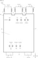
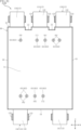
- FIG. 1 is a perspective view of a semiconductor device included in a semiconductor module according to a first embodiment of the present disclosure.
- FIG. 2 is a plan view of the semiconductor device shown in FIG.
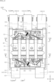
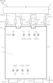
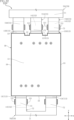
- FIG. 3 is a plan view corresponding to FIG. 2, seen through the sealing resin.
- FIG. 4 is a partially enlarged view of FIG.
- FIG. 5 is a plan view corresponding to FIG. 2, showing the first conductive member through which the sealing resin is omitted.
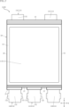
- FIG. 6 is a right side view of the semiconductor device shown in FIG.
- FIG. 7 is a bottom view of the semiconductor device shown in FIG.
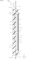
- FIG. 8 is a cross-sectional view taken along line VIII-VIII in FIG.
- FIG. 9 is a cross-sectional view taken along line IX-IX in FIG.
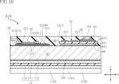
- FIG. 10 is a partial enlarged view of the first element and its periphery shown in FIG.
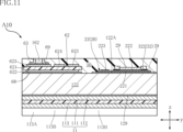
- FIG. 11 is a partial enlarged view of the second element and its periphery shown in FIG.
- FIG. 12 is a cross-sectional view taken along line XII-XII in FIG.
- FIG. 13 is a cross-sectional view taken along line XIII-XIII in FIG.
- FIG. 14 is a partially enlarged view of FIG.
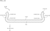
- FIG. 15 is a cross-sectional view taken along line XV-XV in FIG.
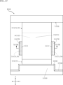
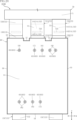
- FIG. 16 is a plan view of the semiconductor module according to the first embodiment of the present disclosure.
- FIG. 17 is a partially enlarged view of FIG.
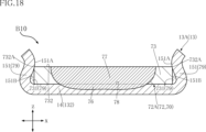
- FIG. 18 is a cross-sectional view taken along line XVIII-XVIII in FIG.
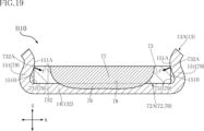
- FIG. 19 is a cross-sectional view illustrating the function and effect of the semiconductor module shown in FIG.
- FIG. 20 is a schematic diagram of a vehicle on which the semiconductor module shown in FIG. 16 is mounted.
- FIG. 21 is a plan view of a semiconductor module according to the second embodiment of the present disclosure.
- FIG. 22 is a partially enlarged view of FIG.
- FIG. 23 is a cross-sectional view taken along line XXIII-XXIII in FIG.
- FIG. 24 is a plan view of a semiconductor module according to a third embodiment of the present disclosure.
- FIG. 25 is a partially enlarged view of FIG.
- FIG. 26 is a cross-sectional view taken along line XXVI-XXVI in FIG.
- FIG. 27 is a cross-sectional view taken along line XXVII-XXVII in FIG.
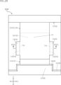
- FIG. 28 is a plan view of a semiconductor module according to a fourth embodiment of the present disclosure.
- FIG. 29 is a partially enlarged view of FIG.
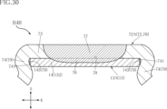
- FIG. 30 is a cross-sectional view taken along line XXX-XXX in FIG.
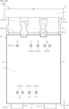
- FIG. 31 is a plan view of a semiconductor device included in a semiconductor module according to a fifth embodiment of the present disclosure.
- FIG. 32 is a plan view of a semiconductor module according to a fifth embodiment of the present disclosure.
- the semiconductor device A10 includes a first conductive layer 121, a second conductive layer 122, a plurality of power terminals 13, a plurality of semiconductor elements 20, a first conductive member 31, a second conductive member 32, and a sealing resin 50.
- the semiconductor device A10 further includes a base material 11, a first signal terminal 161, a second signal terminal 162, a third signal terminal 171, a fourth signal terminal 172, two fifth signal terminals 181, two sixth signal terminals 182, a seventh signal terminal 191, two thermistors 23, a first wiring 61, and a second wiring 62.
- FIG. 4 shows the sealing resin 50 through for ease of understanding.
- the through sealing resin 50 is shown by an imaginary line (two-dot chain line).
- FIG. 5 shows the first conductive member 31 in a see-through manner and omits the sealing resin 50 .
- first direction z the normal direction of the first main surface 121A of the first conductive layer 121 described below
- second direction x One direction that is orthogonal to the first direction z
- third direction y The direction that is orthogonal to both the first direction z and the second direction x
- the semiconductor device A10 converts DC power input to the first power terminal 13A and the two second power terminals 13B into AC power using multiple semiconductor elements 20.
- the converted AC power is input to a power supply target such as a motor from each of the two third power terminals 13C.
- the substrate 11 is located on the opposite side of the multiple semiconductor elements 20 in the first direction z with the first conductive layer 121 and the second conductive layer 122 as references.
- the substrate 11 supports the first conductive layer 121 and the second conductive layer 122.
- the substrate 11 is composed of a DBC (Direct Bonded Copper) substrate.
- the substrate 11 includes an insulating layer 111, two intermediate layers 112, and a heat dissipation layer 113.
- the substrate 11 is covered with a sealing resin 50 except for a portion of the heat dissipation layer 113.
- the insulating layer 111 includes a portion interposed between the intermediate layer 112 and the heat dissipation layer 113 in the first direction z.
- the insulating layer 111 is made of a material with relatively high thermal conductivity.
- the insulating layer 111 is made of ceramics including aluminum nitride (AlN), for example.
- the insulating layer 111 may be made of an insulating resin sheet in addition to ceramics.
- the dimension of the insulating layer 111 in the first direction z is smaller than the dimension of each of the first conductive layer 121 and the second conductive layer 122 in the first direction z.
- the two intermediate layers 112 are located between the insulating layer 111 and the first conductive layer 121 and second conductive layer 122 in the first direction z.
- the intermediate layers 112 are spaced apart from each other in the third direction y.
- the composition of the intermediate layer 112 includes copper (Cu).
- the intermediate layer 112 is surrounded by the periphery of the insulating layer 111 when viewed in the first direction z.
- the heat dissipation layer 113 is located on the opposite side of the insulating layer 111 from the two intermediate layers 112 in the first direction z. As shown in Figure 7, the heat dissipation layer 113 is exposed from the sealing resin 50.
- the composition of the heat dissipation layer 113 includes copper.
- the dimension of the heat dissipation layer 113 in the first direction z is larger than the dimension of the insulating layer 111 in the first direction z.
- the heat dissipation layer 113 is surrounded by the periphery of the insulating layer 111.
- the first conductive layer 121 and the second conductive layer 122 are bonded to the substrate 11 as shown in Figures 9 to 11.
- the composition of the first conductive layer 121 and the second conductive layer 122 includes copper.
- the first conductive layer 121 and the second conductive layer 122 are separated from each other in the third direction y.
- the first conductive layer 121 has a first main surface 121A facing the first direction z.
- the first main surface 121A faces the multiple semiconductor elements 20.
- the first conductive layer 121 is bonded to one of the two intermediate layers 112 via a first bonding layer 129.
- the first bonding layer 129 is, for example, solder.
- the second conductive layer 122 has a second main surface 122A facing the same side as the first main surface 121A in the first direction z. As shown in FIG. 11, the second conductive layer 122 is bonded to the other of the two intermediate layers 112 via a first bonding layer 129.
- each of the multiple semiconductor elements 20 is mounted on either the first conductive layer 121 or the second conductive layer 122.
- the multiple semiconductor elements 20 are, for example, MOSFETs (Metal-Oxide-Semiconductor Field-Effect Transistors).
- the multiple semiconductor elements 20 may be switching elements such as IGBTs (Insulated Gate Bipolar Transistors) or diodes.
- IGBTs Insulated Gate Bipolar Transistors
- the multiple semiconductor elements 20 are n-channel type MOSFETs with a vertical structure.
- the multiple semiconductor elements 20 include a compound semiconductor substrate.
- the composition of the compound semiconductor substrate includes silicon carbide (SiC).
- the multiple semiconductor elements 20 include multiple first semiconductor elements 21 and multiple second semiconductor elements 22.
- the structure of each of the multiple second semiconductor elements 22 is equal to the structure of each of the multiple first semiconductor elements 21.
- the multiple first semiconductor elements 21 are mounted on the first main surface 121A of the first conductive layer 121.
- the multiple first semiconductor elements 21 are arranged along the second direction x.
- the multiple second semiconductor elements 22 are mounted on the second main surface 122A of the second conductive layer 122.
- the multiple second semiconductor elements 22 are arranged along the second direction x.
- each of the multiple first semiconductor elements 21 has a first electrode 211, a second electrode 212, a first gate electrode 213, and a first detection electrode 214.
- the first electrode 211 faces the first main surface 121A of the first conductive layer 121.
- a current corresponding to the power before being converted by the first semiconductor element 21 flows through the first electrode 211.
- the first electrode 211 corresponds to the drain electrode of the first semiconductor element 21.
- the first electrode 211 is conductively bonded to the first main surface 121A via the conductive bonding layer 29.
- the first electrode 211 of each of the multiple first semiconductor elements 21 is electrically connected to the first conductive layer 121.
- the conductive bonding layer 29 is a sintered metal containing silver (Ag) or the like. Alternatively, the conductive bonding layer 29 may be solder.
- the second electrode 212 is located on the opposite side of the first conductive layer 121 facing the first main surface 121A in the first direction z. Therefore, the first electrode 211 and the second electrode 212 are located on opposite sides of each other in the first direction z. A current corresponding to the power converted by the first semiconductor element 21 flows through the second electrode 212. In other words, the second electrode 212 corresponds to the source electrode of the first semiconductor element 21.
- the first gate electrode 213 is located on the opposite side to the side facing the first main surface 121A of the first conductive layer 121 in the first direction z. Therefore, the first gate electrode 213 is located on the same side as the second electrode 212 in the first direction z.
- a gate voltage for driving the first semiconductor element 21 is applied to the first gate electrode 213.
- the area of the first gate electrode 213 is smaller than the area of the second electrode 212 when viewed in the first direction z.
- the first detection electrode 214 is located on the same side as the second electrode 212 and the first gate electrode 213 in the first direction z.
- the first detection electrode 214 is located next to the first gate electrode 213 in the second direction x.
- a voltage equivalent to the voltage applied to the second electrode 212 is applied to the first detection electrode 214.
- the area of the first detection electrode 214 is equal (or approximately equal) to the area of the first gate electrode 213.
- each of the multiple second semiconductor elements 22 has a third electrode 221, a fourth electrode 222, a second gate electrode 223, and a second detection electrode 224.
- the third electrode 221 faces the second main surface 122A of the second conductive layer 122.
- a current corresponding to the power before being converted by the second semiconductor element 22 flows through the third electrode 221.
- the third electrode 221 corresponds to the drain electrode of the second semiconductor element 22.
- the third electrode 221 is conductively bonded to the second main surface 122A via the conductive bonding layer 29.
- the third electrode 221 of each of the multiple second semiconductor elements 22 is electrically connected to the second conductive layer 122.
- the fourth electrode 222 is located on the opposite side to the side facing the second main surface 122A of the second conductive layer 122 in the first direction z. Therefore, the third electrode 221 and the fourth electrode 222 are located on opposite sides to each other in the first direction z. A current corresponding to the power converted by the second semiconductor element 22 flows through the fourth electrode 222. In other words, the fourth electrode 222 corresponds to the source electrode of the second semiconductor element 22.
- the second gate electrode 223 is located on the opposite side to the side facing the second main surface 122A of the second conductive layer 122 in the first direction z. Therefore, the second gate electrode 223 is located on the same side as the fourth electrode 222 in the first direction z.
- a gate voltage for driving the second semiconductor element 22 is applied to the second gate electrode 223.
- the area of the second gate electrode 223 is smaller than the area of the fourth electrode 222 when viewed in the first direction z.
- the second detection electrode 224 is located on the same side as the fourth electrode 222 and the second gate electrode 223 in the first direction z.
- the second detection electrode 224 is located on both sides of the second gate electrode 223 in the second direction x.
- a voltage equivalent to the voltage applied to the fourth electrode 222 is applied to the second detection electrode 224.
- the area of the second detection electrode 224 is equal (or approximately equal) to the area of the second gate electrode 223.
- each of the multiple power terminals 13 is exposed to the outside from the sealing resin 50.
- Each of the multiple power terminals 13 is electrically connected to one of the multiple semiconductor elements 20.
- the multiple power terminals 13 include a first power terminal 13A, two second power terminals 13B, and two third power terminals 13C.
- Each of the multiple power terminals 13 has an internal connection portion 131 and an external connection portion 132.
- the internal connection portion 131 is covered by the sealing resin 50.
- the external connection portion 132 extends from the internal connection portion 131 in the third direction y and is exposed to the outside from the sealing resin 50.
- the first power terminal 13A is located on the opposite side of the second conductive layer 122 with respect to the first conductive layer 121 in the third direction y.
- the first power terminal 13A is conductively joined to the first conductive layer 121.
- the first power terminal 13A is electrically connected to the first electrodes 211 of each of the multiple first semiconductor elements 21 via the first conductive layer 121.
- the first power terminal 13A extends from the first conductive layer 121 in the third direction y.
- the internal connection portion 131 of the first power terminal 13A is conductively joined to the first conductive layer 121.
- each of the two second power terminals 13B is located on the same side as the first power terminal 13A in the third direction y with respect to the first conductive layer 121 and the second conductive layer 122, and is spaced apart from the first conductive layer 121 and the second conductive layer 122.
- Each of the two second power terminals 13B is electrically connected to the fourth electrode 222 of each of the multiple second semiconductor elements 22.
- the two second power terminals 13B are spaced apart from each other in the second direction x.
- the first power terminal 13A is located between the two second power terminals 13B in the second direction x.
- the internal connection portion 131 of each of the two second power terminals 13B is spaced apart from the first conductive layer 121.
- the first power terminal 13A is a P-terminal (positive pole) to which DC power to be converted is input
- the two second power terminals 13B are N-terminals (positive poles) to which DC power to be converted is input.
- the conductive paths of the semiconductor device A10 to the multiple semiconductor elements 20 may be appropriately changed so that the first power terminal 13A is an N-terminal and the two second power terminals 13B are P-terminals.
- each of the two third power terminals 13C is located on the opposite side of the first conductive layer 121 with respect to the second conductive layer 122 in the third direction y.
- Each of the two third power terminals 13C is conductively joined to the second conductive layer 122.
- each of the two third power terminals 13C is electrically connected to the third electrodes 221 of the multiple second semiconductor elements 22 via the second conductive layer 122.
- AC power converted by the multiple semiconductor elements 20 is output from each of the two third power terminals 13C.
- the two third power terminals 13C are separated from each other in the second direction x.
- the internal connection portion 131 of each of the two third power terminals 13C is conductively joined to the second conductive layer 122.
- each of the multiple power terminals 13 has an engagement portion 133 exposed to the outside from the sealing resin 50.
- the first power terminal 13A and the two second power terminals 13B each have an engagement portion 133.
- the engagement portion 133 is connected to the external connection portion 132.
- the external connection portion 132 of each of the multiple power terminals 13 has a connection surface 132A.
- the connection surface 132A faces the same side as the first main surface 121A of the first conductive layer 121 in the first direction z.
- the engagement portion 133 has an engagement surface 134 that faces the side where the connection surface 132A is located in the second direction x.
- the engagement portion 133 includes a pair of wall portions 133A.
- Each of the pair of wall portions 133A protrudes in the first direction z from both sides of the external connection portion 132 in the second direction x.
- the pair of wall portions 133A protrude in the first direction z toward the side toward which the connection surface 132A faces.
- Each of the pair of wall portions 133A has an engagement surface 134.
- the engagement surface 134 includes a first region 134A and a second region 134B.
- the second region 134B is located on the opposite side of the external connection part 132 with respect to the first region 134A in the first direction z.
- the first region 134A is concave and recessed in the direction away from the connection surface 132A of the external connection part 132 in the second direction x.
- the second region 134B is convex and protrudes in the direction toward the connection surface 132A in the second direction x.
- the first wiring 61 is joined to the first main surface 121A of the first conductive layer 121, as shown in FIG. 10.
- the first wiring 61 is located on the opposite side of the multiple second semiconductor elements 22 with respect to the multiple first semiconductor elements 21 in the third direction y.
- the first wiring 61 is electrically connected to the multiple first semiconductor elements 21 and the first conductive layer 121.
- the first wiring 61 has a first mounting layer 611, a first metal layer 612, two first gate wiring layers 613, a first detection wiring layer 614, a first temperature detection wiring layer 615, and a second detection wiring layer 616.
- the first mounting layer 611 includes two first gate wiring layers 613, a first detection wiring layer 614, two first temperature detection wiring layers 615, and a second detection wiring layer 616.
- the first mounting layer 611 is an insulator.
- the first mounting layer 611 is made of ceramics, for example. Alternatively, the first mounting layer 611 may be made of an insulating resin sheet.
- the first metal layer 612 is located on the side facing the first main surface 121A of the first conductive layer 121 with the first mounting layer 611 as a reference in the first direction z.
- the first metal layer 612 is bonded to the first mounting layer 611.
- the composition of the first metal layer 612 includes copper.
- the first metal layer 612 is bonded to the first main surface 121A via a second bonding layer 68.
- the second bonding layer 68 is, for example, solder.
- the two first gate wiring layers 613 are located on the opposite side of the first metal layer 612 with respect to the first mounting layer 611.
- the two first gate wiring layers 613 are bonded to the first mounting layer 611.
- one of the first gate wiring layers 613 has a plurality of first wires 41 conductively bonded thereto.
- the plurality of first wires 41 are individually conductively bonded to the first gate electrodes 213 of the plurality of first semiconductor elements 21.
- a plurality of sixth wires 46 are conductively bonded to each of the two first gate wiring layers 613.
- each of the two first gate wiring layers 613 is electrically connected to the first gate electrodes 213 of the plurality of first semiconductor elements 21.
- the first detection wiring layer 614 is located on the opposite side of the first metal layer 612 with respect to the first mounting layer 611.
- the first detection wiring layer 614 is bonded to the first mounting layer 611.
- a plurality of second wires 42 are conductively bonded to the first detection wiring layer 614.
- the plurality of second wires 42 are individually conductively bonded to the first detection electrodes 214 of each of the plurality of first semiconductor elements 21.
- the first detection wiring layer 614 is electrically connected to the first detection electrodes 214 of each of the plurality of first semiconductor elements 21.
- the two first temperature detection wiring layers 615 are located on the opposite side of the first metal layer 612 with respect to the first mounting layer 611.
- the two first temperature detection wiring layers 615 are bonded to the first mounting layer 611.
- the two first temperature detection wiring layers 615 are adjacent to each other in the second direction x.
- the second detection wiring layer 616 is located on the opposite side to the first metal layer 612 with respect to the first mounting layer 611.
- the second detection wiring layer 616 is bonded to the first mounting layer 611.
- the third wire 43 is conductively bonded to the second detection wiring layer 616.
- the third wire 43 is further conductively bonded to the first main surface 121A of the first conductive layer 121.
- the second detection wiring layer 616 is electrically connected to the first conductive layer 121.
- the second wiring 62 is joined to the second main surface 122A of the second conductive layer 122, as shown in FIG. 11.
- the second wiring 62 is located on the opposite side of the multiple first semiconductor elements 21 with respect to the multiple second semiconductor elements 22 in the third direction y.
- the second wiring 62 is electrically connected to the multiple second semiconductor elements 22 and the second conductive layer 122.
- the second wiring 62 has a second mounting layer 621, a second metal layer 622, two second gate wiring layers 623, a third detection wiring layer 624, two second temperature detection wiring layers 625, and a fourth detection wiring layer 626.
- the second mounting layer 621 includes two second gate wiring layers 623, a third detection wiring layer 624, two second temperature detection wiring layers 625, and a fourth detection wiring layer 626.
- the second mounting layer 621 is an insulator.
- the second mounting layer 621 is made of ceramics, for example. Alternatively, the second mounting layer 621 may be made of an insulating resin sheet.
- the second metal layer 622 is located on the side facing the second main surface 122A of the second conductive layer 122 with the second mounting layer 621 as a reference in the first direction z.
- the second metal layer 622 is bonded to the second mounting layer 621.
- the composition of the second metal layer 622 includes copper.
- the second metal layer 622 is bonded to the second main surface 122A via the second bonding layer 68.
- the two second gate wiring layers 623 are located on the opposite side of the second metal layer 622 with respect to the second mounting layer 621.
- the two second gate wiring layers 623 are bonded to the second mounting layer 621.
- one of the second gate wiring layers 623 has a plurality of fourth wires 44 conductively bonded thereto.
- the plurality of fourth wires 44 are individually conductively bonded to the second gate electrodes 223 of the plurality of second semiconductor elements 22.
- a plurality of seventh wires 47 are conductively bonded to each of the two second gate wiring layers 623.
- each of the two second gate wiring layers 623 is electrically connected to the second gate electrodes 223 of the plurality of second semiconductor elements 22.
- the third detection wiring layer 624 is located on the opposite side to the second metal layer 622 with respect to the second mounting layer 621.
- the third detection wiring layer 624 is bonded to the second mounting layer 621.
- a plurality of fifth wires 45 are conductively bonded to the third detection wiring layer 624.
- the plurality of fifth wires 45 are individually conductively bonded to the second detection electrodes 224 of each of the plurality of second semiconductor elements 22.
- the third detection wiring layer 624 is electrically connected to the second detection electrodes 224 of each of the plurality of second semiconductor elements 22.
- the two second temperature detection wiring layers 625 are located on the opposite side of the second metal layer 622 with respect to the second mounting layer 621.
- the two second temperature detection wiring layers 625 are bonded to the second mounting layer 621.
- the two second temperature detection wiring layers 625 are adjacent to each other in the second direction x.
- the fourth detection wiring layer 626 is located on the opposite side of the second metal layer 622 with respect to the second mounting layer 621.
- the fourth detection wiring layer 626 is bonded to the second mounting layer 621.
- each of the multiple sleeves 63 is conductively bonded to either the first wiring 61 or the second wiring 62 via a third bonding layer 69.
- the third bonding layer 69 is, for example, solder.
- the multiple sleeves 63 are made of a conductive material such as metal.
- Each of the multiple sleeves 63 is tubular and extends in the first direction z.
- each of the multiple sleeves 63 has an end face 631 that faces the same side as the first main surface 121A of the first conductive layer 121 in the first direction z. The end face 631 is exposed to the outside from the top surface 51 of the sealing resin 50 described later.
- the third bonding layer 69 is, for example, solder.
- One of the two thermistors 23 is conductively joined to the two first temperature detection wiring layers 615 of the first wiring 61 as shown in FIG. 4.
- the other of the two thermistors 23 is conductively joined to the two second temperature detection wiring layers 625 of the second wiring 62 as shown in FIG. 4.
- the two thermistors 23 are used as temperature detection sensors for the semiconductor device A10.
- the first signal terminal 161, the second signal terminal 162, the third signal terminal 171, the fourth signal terminal 172, the two fifth signal terminals 181, the two sixth signal terminals 182, and the seventh signal terminal 191 are made of metal pins extending in the first direction z, as shown in FIG. 1. These terminals protrude from the top surface 51 of the sealing resin 50, which will be described later. Furthermore, these terminals are individually press-fitted into a number of sleeves 63. As a result, each of these terminals is supported by one of the multiple sleeves 63, and is conductive to one of the first wiring 61 and the second wiring 62.
- the first signal terminal 161 is press-fitted into one of the multiple sleeves 63 that is conductively joined to one of the two first gate wiring layers 613 of the first wiring 61. As a result, the first signal terminal 161 is electrically connected to the first gate electrode 213 of each of the multiple first semiconductor elements 21 via the two first gate wiring layers 613. A gate voltage for driving the multiple first semiconductor elements 21 is applied to the first signal terminal 161.
- the second signal terminal 162 is press-fitted into one of the multiple sleeves 63 that is conductively joined to one of the two second gate wiring layers 623 of the second wiring 62.
- the second signal terminal 162 is electrically connected to the second gate electrodes 223 of the multiple second semiconductor elements 22 via the two second gate wiring layers 623.
- a gate voltage for driving the multiple second semiconductor elements 22 is applied to the second signal terminal 162.
- the third signal terminal 171 is located next to the first signal terminal 161 in the second direction x. As shown in FIG. 5, the third signal terminal 171 is press-fitted into one of the multiple sleeves 63 that is conductively joined to the first detection wiring layer 614 of the first wiring 61. As a result, the third signal terminal 171 is electrically connected to the first detection electrode 214 of each of the multiple first semiconductor elements 21 via the first detection wiring layer 614. A voltage equivalent to the voltage applied to the first detection electrode 214 of each of the multiple first semiconductor elements 21 is applied to the third signal terminal 171.
- the fourth signal terminal 172 is located next to the second signal terminal 162 in the second direction x. As shown in FIG. 5, the fourth signal terminal 172 is press-fitted into one of the multiple sleeves 63 that is conductively joined to the third detection wiring layer 624 of the second wiring 62. As a result, the fourth signal terminal 172 is electrically connected to the second detection electrodes 224 of each of the multiple second semiconductor elements 22 via the third detection wiring layer 624. A voltage equivalent to the voltage applied to the second detection electrodes 224 of each of the multiple second semiconductor elements 22 is applied to the fourth signal terminal 172.
- the two fifth signal terminals 181 are located on the opposite side of the third signal terminal 171 in the second direction x with respect to the first signal terminal 161.
- the two fifth signal terminals 181 are adjacent to each other in the second direction x.
- the two fifth signal terminals 181 are individually press-fitted into two of the multiple sleeves 63 that are individually conductively joined to the two first temperature detection wiring layers 615 of the first wiring 61.
- the two fifth signal terminals 181 are electrically connected to the two thermistors 23 that are conductively joined to the two first temperature detection wiring layers 615 of the two thermistors 23.
- the two sixth signal terminals 182 are located on the opposite side of the fourth signal terminal 172 in the second direction x with respect to the second signal terminal 162.
- the two sixth signal terminals 182 are adjacent to each other in the second direction x.
- the two sixth signal terminals 182 are individually press-fitted into two of the multiple sleeves 63 that are individually conductively joined to the two second temperature detection wiring layers 625 of the second wiring 62.
- the two sixth signal terminals 182 are electrically connected to the two thermistors 23 that are conductively joined to the two second temperature detection wiring layers 625 of the two thermistors 23.
- the seventh signal terminal 191 is located on the opposite side of the first signal terminal 161 with respect to the third signal terminal 171 in the second direction x. As shown in FIG. 5, the seventh signal terminal 191 is press-fitted into one of the multiple sleeves 63 that is conductively joined to the second detection wiring layer 616 of the first wiring 61. This allows the seventh signal terminal 191 to be electrically connected to the first conductive layer 121 via the second detection wiring layer 616. A voltage equivalent to the DC power input to the first power terminal 13A and the two second power terminals 13B is applied to the seventh signal terminal 191.
- the first conductive member 31 is conductively joined to the second electrodes 212 of the multiple first semiconductor elements 21 and the second main surface 122A of the second conductive layer 122.
- the second electrodes 212 of the multiple first semiconductor elements 21 are electrically connected to the second conductive layer 122.
- the composition of the first conductive member 31 includes copper.
- the first conductive member 31 is a metal clip.
- the first conductive member 31 has a main body portion 311, multiple first joint portions 312, multiple first connecting portions 313, second joint portions 314 and second connecting portions 315.
- the main body 311 forms the main part of the first conductive member 31. As shown in FIG. 5, the main body 311 extends in the second direction x. As shown in FIG. 9, the main body 311 straddles between the first conductive layer 121 and the second conductive layer 122.
- the multiple first bonding portions 312 are individually bonded to the second electrodes 212 of the multiple first semiconductor elements 21. Each of the multiple first bonding portions 312 faces the second electrodes 212 of one of the multiple first semiconductor elements 21.
- the multiple first connecting portions 313 are connected to the main body portion 311 and the multiple first bonding portions 312.
- the multiple first connecting portions 313 are spaced apart from one another in the second direction x.
- the multiple first connecting portions 313 when viewed in the second direction x, are inclined in a direction away from the first main surface 121A of the first conductive layer 121 as they move from the multiple first bonding portions 312 toward the main body portion 311.
- the second joint 314 is joined to the second main surface 122A of the second conductive layer 122.
- the second joint 314 faces the second main surface 122A.
- the second joint 314 extends in the second direction x.
- the dimension of the second joint 314 in the second direction x is equal to the dimension of the main body portion 311 in the second direction x.
- the second connecting portion 315 is connected to the main body portion 311 and the second joint portion 314.
- the second connecting portion 315 is inclined in a direction away from the second main surface 122A of the second conductive layer 122 as it moves from the second joint portion 314 toward the main body portion 311.
- the dimension of the second connecting portion 315 in the second direction x is equal to the dimension of the main body portion 311 in the second direction x.
- a conductive bonding layer 29 is located between the second electrode 212 of each of the multiple first semiconductor elements 21 and each of the multiple first bonding portions 312.
- the conductive bonding layer 29 conductively bonds each of the multiple first bonding portions 312 to the second electrode 212 of each of the multiple first semiconductor elements 21 individually.
- a conductive bonding layer 29 is located between the second main surface 122A of the second conductive layer 122 and the second bonding portion 314.
- the conductive bonding layer 29 conductively bonds the second main surface 122A to the second bonding portion 314.
- the second conductive member 32 is conductively joined to the second electrodes 212 of the second semiconductor elements 22 and the internal connection portions 131 of the two second power terminals 13B. As a result, the second electrodes 212 of the second semiconductor elements 22 are electrically connected to the two second power terminals 13B.
- the composition of the second conductive member 32 includes copper.
- the second conductive member 32 is a metal clip. As shown in FIG. 4, the second conductive member 32 has two main body portions 321, a plurality of third joint portions 322, a plurality of third connecting portions 323, two fourth joint portions 324, two fourth connecting portions 325, a plurality of intermediate portions 326, and a plurality of cross beam portions 327.
- the two main body portions 321 are spaced apart from each other in the second direction x.
- the two main body portions 321 extend in the third direction y.
- the two main body portions 321 are parallel to the first main surface 121A of the first conductive layer 121 and the second main surface 122A of the second conductive layer 122.
- the two main body portions 321 are spaced apart from the first main surface 121A and the second main surface 122A more than the main body portion 311 of the first conductive member 31.
- the intermediate portions 326 are spaced apart from one another in the second direction x and are located between the two main body portions 321 in the second direction x.
- the intermediate portions 326 extend in the third direction y.
- the dimension of each of the intermediate portions 326 in the third direction y is smaller than the dimension of each of the two main body portions 321 in the third direction y.
- the multiple third bonding portions 322 are individually bonded to the second electrodes 212 of the multiple second semiconductor elements 22. Each of the multiple third bonding portions 322 faces the fourth electrode 222 of one of the multiple second semiconductor elements 22.
- the multiple third connecting portions 323 are connected to both sides of the multiple third joint portions 322 in the second direction x. Furthermore, the multiple third connecting portions 323 are connected to either of the two main body portions 321 or the multiple intermediate portions 326. When viewed in the third direction y, each of the multiple third connecting portions 323 is inclined in a direction away from the second main surface 122A of the second conductive layer 122 as it moves from one of the multiple third joint portions 322 toward one of the two main body portions 321 or the multiple intermediate portions 326.
- the two fourth joints 324 are individually joined to the internal connection parts 131 of the two second power terminals 13B.
- Each of the two fourth joints 324 individually faces the internal connection parts 131 of the two second power terminals 13B in the first direction z.
- the two fourth connecting portions 325 are connected to the two main body portions 321 and the two fourth joint portions 324.
- the two fourth connecting portions 325 are inclined in a direction away from the first main surface 121A of the first conductive layer 121 as they move from the two fourth joint portions 324 toward the two main body portions 321.
- the multiple cross beam portions 327 are arranged along the second direction x.
- the multiple cross beam portions 327 include areas that individually overlap the multiple first joint portions 312 of the first conductive member 31.
- the cross beam portion 327 located at the center in the second direction x is connected to the multiple intermediate portions 326 on both sides in the second direction x.
- the remaining two cross beam portions 327 are connected to one of the two main body portions 321 and one of the multiple intermediate portions 326 on both sides in the second direction x.
- the multiple cross beam portions 327 are convex in the first direction z toward the side toward which the first main surface 121A of the first conductive layer 121 faces.
- a conductive bonding layer 29 is located between each of the fourth electrodes 222 of the multiple second semiconductor elements 22 and each of the multiple third joints 322.
- the conductive bonding layer 29 conductively bonds each of the multiple third joints 322 and each of the multiple second semiconductor elements 22.
- a conductive bonding layer 29 is located between each of the internal connection parts 131 of the two second power terminals 13B and the two fourth joints 324.
- the conductive bonding layer 29 conductively bonds each of the internal connection parts 131 of the two second power terminals 13B and the two fourth joints 324.
- the sealing resin 50 covers the first conductive layer 121, the second conductive layer 122, the multiple semiconductor elements 20, the first conductive member 31 and the second conductive member 32. Furthermore, the sealing resin 50 covers a part of the substrate 11 and a part of each of the multiple power terminals 13.
- the sealing resin 50 has electrical insulation properties.
- the sealing resin 50 is made of a material that contains, for example, black epoxy resin. As shown in Figures 2 and 6 to 9, the sealing resin 50 has a top surface 51, a bottom surface 52, a first side surface 53, a second side surface 54, a third side surface 55, a fourth side surface 56, and two recesses 57.
- the top surface 51 faces the same side as the first main surface 121A of the first conductive layer 121 in the first direction z.
- the bottom surface 52 faces the opposite side to the top surface 51 in the first direction z.
- the heat dissipation layer 113 of the substrate 11 is exposed from the bottom surface 52.
- the first side 53 and the second side 54 are separated from each other in the third direction y.
- the first side 53 and the second side 54 face opposite each other in the third direction y.
- the external connection portion 132 of the first power terminal 13A and the external connection portion 132 of each of the two second power terminals 13B are exposed to the outside.
- the external connection portion 132 of each of the two third power terminals 13C are exposed to the outside.
- the third side 55 and the fourth side 56 are spaced apart from each other in the second direction x.
- the third side 55 and the fourth side 56 face in opposite directions from each other in the second direction x.
- the two recesses 57 are recessed from the first side surface 53 toward the third direction y.
- the two recesses 57 extend from the top surface 51 to the bottom surface 52 in the first direction z.
- the two recesses 57 are located on both sides of the first power terminal 13A in the second direction x.
- the semiconductor module B10 includes a semiconductor device A10 and an external connection member 70.
- the external connection member 70 is individually connected to the first power terminal 13A and the two second power terminals 13B among the multiple power terminals 13.
- the external connection member 70 is a bus bar.
- the external connection member 70 may be a capacitor module.
- the external connection member 70 has a main body 71 and a plurality of connection terminals 72. A portion of each of the plurality of connection terminals 72 is exposed to the outside from the main body 71.
- the plurality of connection terminals 72 include a first connection terminal 72A and two second connection terminals 72B.
- the first connection terminal 72A is connected to the first power terminal 13A and is electrically conductive to the first power terminal 13A.
- the two second connection terminals 72B are individually connected to the two second power terminals 13B and are individually electrically conductive to the two second power terminals 13B.
- the first power terminal 13A and the two second power terminals 13B each have a first connection portion 14.
- the first connection portion 14 is exposed to the outside from the sealing resin 50.
- the first connection portion 14 corresponds to the external connection portion 132 of each of the multiple power terminals 13 described above.
- each of the multiple connection terminals 72 has a second connection portion 73.
- the second connection portion 73 faces either the first power terminal 13A or the first connection portion 14 of each of the two second power terminals 13B in the first direction z.
- the second connection portion 73 is electrically conductive to the first connection portion 14.
- the first connection portion 14 and the second connection portion 73 are in contact with each other.
- the dimension of the first connection portion 14 in the first direction z is smaller than the dimension of the second connection portion 73 in the first direction z.
- the first power terminal 13A and each of the two second power terminals 13B have a pair of wall portions 151.
- the pair of wall portions 151 are located on opposite sides of each other in the second direction x with respect to the second connection portion 73 of one of the multiple connection terminals 72.
- Each of the pair of wall portions 151 is connected to the first connection portion 14.
- the second connection portion 73 of each of the multiple connection terminals 72 has a pair of engagement surfaces 731 and a first surface 732.
- the pair of engagement surfaces 731 individually face the pair of wall portions 151 of the first power terminal 13A and each of the two second power terminals 13B.
- the pair of wall portions 151 individually contact the pair of engagement surfaces 731.
- the first surface 732 faces the opposite side to the side facing either of the first connection portions 14 of the first power terminal 13A and each of the two second power terminals 13B in the first direction z.
- the first surface 732 is connected to the pair of engagement surfaces 731.
- the first surface 732 includes an edge 732A that forms a boundary with either of the pair of engagement surfaces 731. At least one of the pair of wall portions 151 contacts the edge 732A.
- each of the pair of wall portions 151 of the first power terminal 13A and each of the two second power terminals 13B has an opposing surface 151A.
- the opposing surface 151A of each of the pair of wall portions 151 individually faces a pair of engagement surfaces 731 of the second connection portion 73 of one of the multiple connection terminals 72.
- a gap is provided between the opposing surface 151A and one of the pair of engagement surfaces 731.
- the opposing surfaces 151A of each of the pair of wall portions 151 include an inclined region 151B.
- the inclined region 151B is inclined in the first direction z from the first surface 732 of the second connection portion 73 of any of the multiple connection terminals 72 toward the first connection portion 14, and is inclined in the second direction x in a direction away from the second connection portion 73.
- the inclined region 151B is in contact with one of the pair of engagement surfaces 731 of the second connection portion 73.
- the first power terminal 13A, each of the two second power terminals 13B, and each of the multiple connection terminals 72 are provided with an engagement mechanism 79.
- the engagement mechanism 79 of either the first power terminal 13A or the two second power terminals 13B and the engagement mechanism 79 of either of the multiple connection terminals 72 are in contact with each other.
- the engagement mechanism 79 includes at least one of the first connection portion 14 of the first power terminal 13A and one of the two second power terminals 13B, and the second connection portion 73 of one of the multiple connection terminals 72.
- the engagement mechanism 79 includes a pair of wall portions 151 of the first power terminal 13A and one of the two second power terminals 13B, and a pair of engagement surfaces 731 of the second connection portion 73 of one of the multiple connection terminals 72.
- a first welding mark 76 is formed on the first connection portion 14 of the first power terminal 13A and one of the two second power terminals 13B.
- a second welding mark 77 is formed on the second connection portion 73 of one of the multiple connection terminals 72.
- the first welding mark 76 and the second welding mark 77 are traces of solidified molten metal formed on the first connection portion 14 and the second connection portion 73 when the multiple connection terminals 72 are conductively joined to the first power terminal 13A and the two second power terminals 13B by welding using a laser or the like.
- the first welding mark 76 and the second welding mark 77 are connected to each other at the interface 78 between the first connection portion 14 and the second connection portion 73.
- the vehicle C is, for example, an electric vehicle (EV).
- EV electric vehicle
- vehicle C is equipped with an on-board charger 81, a storage battery 82, and a drive system 83.
- Power is supplied to the on-board charger 81 wirelessly from a power supply facility (not shown) installed outdoors. Alternatively, power may be supplied from the power supply facility to the on-board charger 81 via a wired connection.
- the on-board charger 81 is configured with a step-up DC-DC converter. The voltage of the power supplied to the on-board charger 81 is stepped up by the converter and then supplied to the storage battery 82. The stepped-up voltage is, for example, 600V.
- the drive system 83 drives the vehicle C.
- the drive system 83 has an inverter 831 and a drive source 832.
- the semiconductor module B10 constitutes part of the inverter 831.
- the power stored in the storage battery 82 is supplied to the inverter 831.
- the power supplied from the storage battery 82 to the inverter 831 is DC power.
- a step-up DC-DC converter may be further provided between the storage battery 82 and the inverter 831.
- the inverter 831 converts DC power into AC power.
- the inverter 831 including the semiconductor module B10 is conducted to the drive source 832.
- the drive source 832 has an AC motor and a transmission.
- the AC motor rotates and the rotation is transmitted to the transmission.
- the transmission rotates the drive shaft of the vehicle C after appropriately reducing the rotation speed transmitted from the AC motor. This drives vehicle C.
- semiconductor module B10 in inverter 831 is necessary to output AC power with an appropriate frequency change to correspond to the required rotation speed of the AC motor.
- the semiconductor module B10 includes a semiconductor element 20, a power terminal 13 that is electrically connected to the semiconductor element 20, and an external connection member 70 having a connection terminal 72 connected to the power terminal 13.
- the connection terminal 72 is electrically connected to the power terminal 13.
- the power terminal 13 and the connection terminal 72 are each provided with an engagement mechanism 79 that contacts each other.
- connection terminal 72 a larger current can be passed through each of the power terminal 13 and the connection terminal 72. Furthermore, when connecting the connection terminal 72 to the power terminal 13, a jig for temporarily fixing the connection terminal 72 to the power terminal 13 is not required. This allows the welding range for the connection terminal 72 to be further expanded when the connection terminal 72 is conductively joined to the power terminal 13 by welding. Therefore, with this configuration, in the semiconductor module B10, it is possible to suppress misalignment of the connection terminal 72 relative to the power terminal 13, and to improve the bonding state between the power terminal 13 and the connection terminal 72.
- the power terminal 13 has a first connection portion 14 and a pair of wall portions 151.
- the connection terminal 72 has a second connection portion 73 that faces the first connection portion 14 in the first direction z.
- the pair of wall portions 151 are located on opposite sides of each other in the second direction x with respect to the second connection portion 73, and are connected to the first connection portion 14.
- the second connection portion 73 has a pair of engagement surfaces 731 that face the pair of wall portions 151.
- the engagement mechanism 79 includes a pair of walls 151 and a pair of engagement surfaces 731.
- the dimension in the first direction z of the first connection portion 14 of the power terminal 13 is smaller than the dimension in the first direction z of the second connection portion 73 of the connection terminal 72.
- the dimension in the first direction z of each of the pair of engagement surfaces 731 of the second connection portion 73 can be further increased.
- the second connection portion 73 of the connection terminal 72 has a first surface 732 that faces the side opposite the side facing the first connection portion 14 of the power terminal 13 in the first direction z. At least one of the pair of wall portions 151 of the power terminal 13 is in contact with the edge 732A of the first surface 732.
- Each of the pair of wall portions 151 of the power terminal 13 has an opposing surface 151A that individually faces a pair of engagement surfaces 731 of the second connection portion 73 of the connection terminal 72.
- a gap is provided between the opposing surface 151A and one of the pair of engagement surfaces 731.
- the opposing surfaces 151A of the pair of walls 151 of the power terminal 13 include an inclined region 151B.
- the inclined region 151B is inclined in the first direction z from the first surface 732 of the second connection portion 73 of the connection terminal 72 toward the first connection portion 14 of the power terminal 13, and is inclined in the second direction x away from the second connection portion 73.
- the inclined region 151B is in contact with one of the pair of engagement surfaces 731 of the second connection portion 73 of the connection terminal 72.
- a compressive force F shown in FIG. 19 acts from the inclined region 151B to one of the pair of engagement surfaces 731.
- the direction of the compressive force F is inclined with respect to the second direction x.
- the compressive force F includes a component facing the first direction z and a component facing the second direction x. This allows the engagement mechanism 79 to more effectively suppress misalignment of the connection terminal 72 with respect to the power terminal 13.
- the semiconductor device A10 comprises a conductive layer (either the first conductive layer 121 or the second conductive layer 122), a semiconductor element 20 conductively joined to the conductive layer, a power terminal 13 electrically connected to the semiconductor element 20, and a sealing resin 50 covering the conductive layer and the semiconductor element 20.
- the power terminal 13 has an external connection portion 132 and an engagement portion 133 connected to the external connection portion 132.
- the external connection portion 132 has a connection surface 132A facing the first direction z.
- the engagement portion 133 has an engagement surface 134 facing the side where the connection surface 132A is located in the second direction x.
- connection terminal 72 when a connection terminal 72 is connected to the power terminal 13, if the connection terminal 72 attempts to shift in the second direction x, the connection terminal 72 comes into contact with the engagement surface 134. Therefore, with this configuration, in the semiconductor device A10, it is possible to suppress misalignment of the connection terminal 72 relative to the power terminal 13, and to improve the bonding state between the power terminal 13 and the connection terminal 72.
- the engagement portion 133 includes a pair of wall portions 133A protruding in the first direction z from both sides of the external connection portion 132 in the second direction x.
- Each engagement surface 134 of the pair of wall portions 133A includes a first region 134A and a second region 134B.
- the first region 134A is concave in the second direction x, recessing away from the connection surface 132A of the external connection portion 132.
- the second region 134B is convex in the second direction x, protruding toward the connection surface 132A.
- a semiconductor module B20 according to a second embodiment of the present disclosure will be described with reference to Figures 21 to 23.
- elements that are the same as or similar to the semiconductor device A10 and semiconductor module B10 described above are given the same reference numerals, and duplicated descriptions will be omitted.
- semiconductor module B20 the configuration of the first power terminal 13A and each of the two second power terminals 13B differs from that of semiconductor module B10.
- the first power terminal 13A and each of the two second power terminals 13B have a pair of protrusions 152.
- the pair of protrusions 152 are located on the opposite side of the first connection portion 14 of the first power terminal 13A and either of the two second power terminals 13B in the first direction z, with respect to the second connection portion 73 of either of the multiple connection terminals 72.
- the pair of protrusions 152 extend individually in the second direction x from a pair of wall portions 151 of the first power terminal 13A and either of the two second power terminals 13B.
- Each of the pair of protrusions 152 is in contact with the first surface 732 of the second connection portion 73.
- the engagement mechanism 79 includes a pair of wall portions 151 and a pair of protrusions 152 of the first power terminal 13A and one of the two second power terminals 13B, and a pair of engagement surfaces 731 of the second connection portion 73 of one of the multiple connection terminals 72.
- Semiconductor module B20 comprises a semiconductor element 20, a power terminal 13 electrically connected to the semiconductor element 20, and an external connection member 70 having a connection terminal 72 connected to the power terminal 13.
- the connection terminal 72 is electrically connected to the power terminal 13.
- the power terminal 13 and the connection terminal 72 are each provided with an engagement mechanism 79 that brings them into contact with each other. Therefore, with this configuration, even in semiconductor module B20, it is possible to suppress misalignment of the connection terminal 72 relative to the power terminal 13 and to improve the bonding state between the power terminal 13 and the connection terminal 72. Furthermore, by being equipped with a configuration in common with semiconductor module B10, semiconductor module B20 achieves the same effects as semiconductor module B10.
- the power terminal 13 has a pair of overhangs 152 that extend individually in the second direction x from a pair of wall portions 151. Each of the pair of overhangs 152 contacts the second connection portion 73 of the connection terminal 72.
- the engagement mechanism 79 includes the pair of wall portions 151, the pair of overhangs 152, and a pair of engagement surfaces 731 of the second connection portion 73. This configuration allows a support force in the first direction z to be applied to the second connection portion 73 from each of the pair of overhangs 152. This makes it possible to more effectively suppress the positional deviation of the connection terminal 72 relative to the power terminal 13 while increasing the bonding strength of the connection terminal 72 relative to the power terminal 13. In this case, when the support force in the first direction z acting on the second connection portion 73 becomes larger, it is possible to eliminate the need for conductive bonding by welding between the power terminal 13 and the connection terminal 72.
- a semiconductor module B30 according to a third embodiment of the present disclosure will be described with reference to Figures 24 to 27.
- elements that are the same as or similar to the semiconductor device A10 and semiconductor module B10 described above are given the same reference numerals, and duplicated descriptions will be omitted.
- semiconductor module B30 the configuration of each of the first power terminal 13A and the two second power terminals 13B, and the configuration of each of the multiple connection terminals 72 are different from those of semiconductor module B10.
- the first connection portion 14 of each of the first power terminal 13A and the two second power terminals 13B has a base 141 and a protrusion 142.
- the base 141 is connected to the internal connection portion 131 of either the first power terminal 13A or the two second power terminals 13B.
- the protrusion 142 protrudes from the base 141 toward the second connection portion 73 of either of the multiple connection terminals 72.
- the second connection portion 73 of each of the multiple connection terminals 72 has an inner circumferential surface 733.
- the inner circumferential surface 733 surrounds the convex portion 142 of the first connection portion 14 of the first power terminal 13A and either of the two second power terminals 13B in the first direction z.
- the convex portion 142 is in contact with the inner circumferential surface 733.
- the convex portion 142 is housed in a recess of the second connection portion 73 defined by the inner circumferential surface 733.
- the engagement mechanism 79 includes the convex portion 142 of the first connection portion 14 of the first power terminal 13A and one of the two second power terminals 13B, and the inner surface 733 of the second connection portion 73 of one of the multiple connection terminals 72.
- Semiconductor module B30 includes a semiconductor element 20, a power terminal 13 that is electrically connected to the semiconductor element 20, and an external connection member 70 having a connection terminal 72 connected to the power terminal 13.
- the connection terminal 72 is electrically connected to the power terminal 13.
- the power terminal 13 and the connection terminal 72 are each provided with an engagement mechanism 79 that brings them into contact with each other. Therefore, with this configuration, even in semiconductor module B30, it is possible to suppress misalignment of the connection terminal 72 relative to the power terminal 13, and to improve the bonding state between the power terminal 13 and the connection terminal 72.
- the first connection portion 14 of the power terminal 13 has a base 141 and a protrusion 142 that protrudes from the base 141 toward the second connection portion 73 of the connection terminal 72.
- the second connection portion 73 has an inner surface 733 that surrounds the protrusion 142 around the first direction z.
- the engagement mechanism 79 includes the protrusion 142 and the inner surface 733.
- a semiconductor module B40 according to a fourth embodiment of the present disclosure will be described with reference to Fig. 28 to Fig. 30.
- elements that are the same as or similar to the semiconductor device A10 and semiconductor module B10 described above are given the same reference numerals, and duplicated descriptions will be omitted.
- semiconductor module B40 the configuration of each of the first power terminal 13A and the two second power terminals 13B, and the configuration of each of the multiple connection terminals 72 are different from those of semiconductor module B10.
- each of the multiple connection terminals 72 has a pair of wall portions 74.
- the pair of wall portions 74 protrude in the first direction z from both sides of the second connection portion 73 in the second direction x toward the side where the first connection portion 14 of the first power terminal 13A and one of the two second power terminals 13B is located.
- the pair of wall portions 74 face the first connection portion 14.
- the first connection portion 14 of each of the first power terminal 13A and the two second power terminals 13B has a pair of engagement surfaces 143.
- the pair of engagement surfaces 143 individually face a pair of wall portions 74 of one of the multiple connection terminals 72.
- each of the pair of wall portions 74 of each of the multiple connection terminals 72 has an opposing surface 741.
- the opposing surface 741 faces one of the pair of engagement surfaces 143 and is in contact with the engagement surfaces 143.
- the engagement mechanism 79 includes a pair of engagement surfaces 143 of the first connection portion 14 of the first power terminal 13A and one of the two second power terminals 13B, and a pair of wall portions 74 of one of the multiple connection terminals 72.
- Semiconductor module B40 includes a semiconductor element 20, a power terminal 13 that is electrically connected to the semiconductor element 20, and an external connection member 70 having a connection terminal 72 connected to the power terminal 13.
- the connection terminal 72 is electrically connected to the power terminal 13.
- the power terminal 13 and the connection terminal 72 are each provided with an engagement mechanism 79 that brings them into contact with each other. Therefore, with this configuration, even in semiconductor module B40, it is possible to suppress misalignment of the connection terminal 72 relative to the power terminal 13, and to improve the bonding state between the power terminal 13 and the connection terminal 72.
- a semiconductor device A20 included in a semiconductor module B50 according to a fifth embodiment of the present disclosure will be described with reference to Fig. 31.
- elements that are the same as or similar to those in the semiconductor device A10 and semiconductor module B10 described above are given the same reference numerals, and duplicated descriptions will be omitted.
- semiconductor device A20 the configuration of the multiple power terminals 13 is different from that of semiconductor device A10.
- the first power terminal 13A, the two second power terminals 13B, and the two third power terminals 13C each have an engagement portion 133.
- the configuration of the engagement portion 133 of each of the two third power terminals 13C is the same as the configuration of the engagement portion 133 of the first power terminal 13A and each of the two second power terminals 13B.
- the semiconductor module B50 includes a semiconductor device A20 and an external connection member 70.
- the external connection member 70 includes a first connection member 701 and a second connection member 702.
- the configuration of the first connection member 701 is the same as the configuration of the external connection member 70 provided in the semiconductor module B10.
- the second connection member 702 is individually connected to two third power terminals 13C of the multiple power terminals 13.
- the second connection member 702 is a bus bar that is electrically connected to a motor or the like.
- the first connection member 701 has a main body 71 and multiple connection terminals 72.
- the multiple connection terminals 72 are individually connected to the first power terminal 13A and two second power terminals 13B of the multiple power terminals 13, and are individually conductive to the first power terminal 13A and two second power terminals 13B.
- the second connection member 702 has a main body 71 and two connection terminals 72. Each of the two connection terminals 72 is connected to the main body 71. The two connection terminals 72 are individually connected to the two third power terminals 13C and are individually conductive to the two third power terminals 13C.
- each of the two third power terminals 13C has a first connection portion 14.
- the configuration of the first connection portion 14 of each of the two third power terminals 13C is the same as the configuration of the first connection portion 14 of the first power terminal 13A and each of the two second power terminals 13B.
- each of the two connection terminals 72 of the second connection member 702 has a second connection portion 73.
- the second connection portion 73 faces one of the two third power terminals 13C in the first direction z.
- the configuration of the second connection portion 73 of the second connection member 702 is the same as the configuration of the second connection portion 73 of the external connection member 70 provided in the semiconductor module B10.
- each of the two third power terminals 13C has a pair of wall portions 151.
- the pair of wall portions 151 are located on opposite sides of each other in the second direction x with respect to the second connection portion 73 of one of the two connection terminals 72 of the second connection member 702.
- the configuration of the pair of wall portions 151 of each of the two third power terminals 13C is the same as the configuration of the pair of wall portions 151 of each of the first power terminal 13A and the second power terminal 13B.
- Semiconductor module B50 includes a semiconductor element 20, a power terminal 13 that is electrically connected to the semiconductor element 20, and an external connection member 70 having a connection terminal 72 connected to the power terminal 13.
- the connection terminal 72 is electrically connected to the power terminal 13.
- the power terminal 13 and the connection terminal 72 are each provided with an engagement mechanism 79 that brings them into contact with each other. Therefore, with this configuration, even in semiconductor module B50, it is possible to suppress misalignment of the connection terminal 72 relative to the power terminal 13, and to improve the bonding state between the power terminal 13 and the connection terminal 72.
- Appendix 1 A semiconductor element; a power terminal in electrical communication with the semiconductor element; an external connection member having a connection terminal connected to the power terminal; the connection terminal is electrically connected to the power terminal,
- the semiconductor module wherein the power terminals and the connection terminals are each provided with an engagement mechanism for contacting each other.
- Appendix 2. The power terminal has a first connection portion, the connection terminal has a second connection portion facing the first connection portion in a first direction and electrically connected to the first connection portion; 2.
- Appendix 3. 3. The semiconductor module of claim 2, wherein the first connection portion and the second connection portion are in contact with each other.
- the power terminals are located on opposite sides of the second connection portion in a second direction perpendicular to the first direction, and include a pair of wall portions connected to the first connection portion; the second connection portion has a pair of engagement surfaces that face the pair of wall portions, 4.
- Appendix 5. The semiconductor module of claim 4, wherein a dimension of the first connection portion in the first direction is smaller than a dimension of the second connection portion in the first direction. Appendix 6.
- the second connection portion has a first surface that faces a side opposite to a side facing the first connection portion in the first direction and is connected to the pair of engagement surfaces; the first surface includes an edge that interfaces with one of the pair of engagement surfaces; 6.
- Each of the pair of wall portions has an opposing surface that individually faces the pair of engagement surfaces, 7.
- Appendix 8. 8 The semiconductor module of claim 7, wherein the opposing surface includes an inclined region that slopes away from the second connection portion in the second direction as it moves from the first surface toward the first connection portion in the first direction.
- the inclined region is in contact with one of the pair of engagement surfaces.
- Appendix 10. the power terminal is located on an opposite side of the first connection portion with respect to the second connection portion in the first direction, and has a pair of protruding portions each extending in the second direction from the pair of wall portions, 6. The semiconductor module according to claim 5, wherein each of the pair of protrusions is in contact with the second connection portion.
- Appendix 11. the first connection portion has a base portion and a protrusion portion protruding from the base portion toward the second connection portion, the second connection portion has an inner circumferential surface surrounding the protrusion in the first direction, 4.
- a first welding mark is formed on the first connection portion
- a second welding mark is formed on the second connection portion
- Appendix 13 Further comprising a conductive layer; 13.
- the semiconductor module of claim 12, wherein each of the semiconductor element and the power terminal is conductively bonded to the conductive layer.
- Appendix 14 a sealing resin that covers the conductive layer and the semiconductor element, 14.
- the semiconductor module according to claim 13, wherein the first connection portion is exposed to the outside from the sealing resin.
- Appendix 15. A driving source; A semiconductor module according to any one of Supplementary Notes 3 to 11, The semiconductor module is electrically connected to the drive source.
- the external connection portion has a connection surface facing a first direction,
- the engaging portion has an engaging surface that faces a side on which the connecting surface is located in a second direction perpendicular to the first direction.
- the engagement surface includes a first region and a second region located on an opposite side to the external connection portion with respect to the first region in the first direction, the first region is recessed in a direction away from the connection surface in the second direction, 18.
- the second region is convex and protrudes toward the connection surface in the second direction.
Landscapes
- Inverter Devices (AREA)
Abstract
Description
図1~図15に基づき、本開示の第1実施形態にかかる半導体モジュールB10が具備する半導体装置A10について説明する。半導体装置A10は、第1導電層121、第2導電層122、複数の電力端子13、複数の半導体素子20、第1導通部材31、第2導通部材32および封止樹脂50を備える。さらに半導体装置A10は、基材11、第1信号端子161、第2信号端子162、第3信号端子171、第4信号端子172、2つの第5信号端子181、2つの第6信号端子182、第7信号端子191、2つのサーミスタ23、第1配線61および第2配線62を備える。ここで、図3および図4では、理解の便宜上、封止樹脂50を透過している。図3では、透過した封止樹脂50を想像線(二点鎖線)で示している。図5では、理解の便宜上、第1導通部材31を透過し、かつ封止樹脂50の図示を省略している。
図21~図23に基づき、本開示の第2実施形態にかかる半導体モジュールB20について説明する。これらの図において、先述した半導体装置A10および半導体モジュールB10と同一または類似の要素には同一の符号を付して、重複する説明を省略する。
図24~図27に基づき、本開示の第3実施形態にかかる半導体モジュールB30について説明する。これらの図において、先述した半導体装置A10および半導体モジュールB10と同一または類似の要素には同一の符号を付して、重複する説明を省略する。
図28~図30に基づき、本開示の第4実施形態にかかる半導体モジュールB40について説明する。これらの図において、先述した半導体装置A10および半導体モジュールB10と同一または類似の要素には同一の符号を付して、重複する説明を省略する。
図31に基づき、本開示の第5実施形態にかかる半導体モジュールB50が具備する半導体装置A20について説明する。本図において、先述した半導体装置A10および半導体モジュールB10と同一または類似の要素には同一の符号を付して、重複する説明を省略する。
付記1.
半導体素子と、
前記半導体素子に導通する電力端子と、
前記電力端子に接続された接続端子を有する外部接続部材と、を備え、
前記接続端子は、前記電力端子に導通しており、
前記電力端子および前記接続端子の各々には、互いに接する係合機構が設けられている、半導体モジュール。
付記2.
前記電力端子は、第1接続部を有し、
前記接続端子は、第1方向において前記第1接続部に対向するとともに、前記第1接続部に導通する第2接続部を有し、
前記係合機構は、前記第1接続部および前記第2接続部の少なくともいずれかを含む、付記1に記載の半導体モジュール。
付記3.
前記第1接続部と前記第2接続部とは、互いに接している、付記2に記載の半導体モジュール。
付記4.
前記電力端子は、前記第1方向に対して直交する第2方向において前記第2接続部を基準として互いに反対側に位置するとともに、前記第1接続部につながる一対の壁部を有し、
前記第2接続部は、前記一対の壁部に個別に対向する一対の係合面を有し、
前記係合機構は、前記一対の壁部、および前記一対の係合面を含む、付記3に記載の半導体モジュール。
付記5.
前記第1接続部の前記第1方向の寸法は、前記第2接続部の前記第1方向の寸法よりも小さい、付記4に記載の半導体モジュール。
付記6.
前記第2接続部は、前記第1方向において前記第1接続部に対向する側とは反対側を向くとともに、前記一対の係合面につながる第1面を有し、
前記第1面は、前記一対の係合面のいずれかとの境界をなす端縁を含み、
前記一対の壁部の少なくともいずれかは、前記端縁に接している、付記5に記載の半導体モジュール。
付記7.
前記一対の壁部の各々は、前記一対の係合面に個別に対向する対向面を有し、
前記対向面と前記一対の係合面のいずれかとの間には、隙間が設けられている、付記6に記載の半導体モジュール。
付記8.
前記対向面は、前記第1方向において前記第1面から前記第1接続部に向かうほど、前記第2方向において前記第2接続部から離れる向きに傾斜した傾斜領域を含む、付記7に記載の半導体モジュール。
付記9.
前記傾斜領域は、前記一対の係合面のいずれかに接している、付記8に記載の半導体モジュール。
付記10.
前記電力端子は、前記第1方向において前記第2接続部を基準として前記第1接続部とは反対側に位置するとともに、前記一対の壁部から前記第2方向に個別に延びる一対の張出部を有し、
前記一対の張出部の各々は、前記第2接続部に接している、付記5に記載の半導体モジュール。
付記11.
前記第1接続部は、基部と、前記基部から前記第2接続部に向けて突出する凸部と、を有し、
前記第2接続部は、前記第1方向の回りに前記凸部を囲む内周面を有し、
前記係合機構は、前記凸部および前記内周面を含む、付記3に記載の半導体モジュール。
付記12.
前記第1接続部には、第1溶接痕が形成されており、
前記第2接続部には、第2溶接痕が形成されており、
前記第1溶接痕および前記第2溶接痕は、前記第1接続部と前記第2接続部との界面において互いにつながっている、付記3ないし11のいずれかに記載の半導体モジュール。
付記13.
導電層をさらに備え、
前記半導体素子および前記電力端子の各々は、前記導電層に導電接合されている、付記12に記載の半導体モジュール。
付記14.
前記導電層および前記半導体素子を覆う封止樹脂をさらに備え、
前記第1接続部は、前記封止樹脂から外部に露出している、付記13に記載の半導体モジュール。
付記15.
駆動源と、
付記3ないし11のいずれかに記載の半導体モジュールと、を備え、
前記半導体モジュールは、前記駆動源に導通している、車両。
付記16.
導電層と、
前記導電層に導電接合された半導体素子と、
前記半導体素子に導通する電力端子と、
前記導電層および前記半導体素子を覆う封止樹脂と、を備え、
前記電力端子は、各々が前記封止樹脂から外部に露出する外部接続部および係合部を有し、
前記係合部は、前記外部接続部につながっており、
前記外部接続部は、第1方向を向く接続面を有し、
前記係合部は、前記第1方向に対して直交する第2方向において前記接続面が位置する側を向く係合面を有する、半導体装置。
付記17.
前記係合部は、前記外部接続部の前記第2方向の両側から前記第1方向に突出する一対の壁部を含む、付記16に記載の半導体装置。
付記18.
前記係合面は、第1領域と、前記第1方向において前記第1領域を基準として前記外部接続部とは反対側に位置する第2領域と、を含み、
前記第1領域は、前記第2方向において前記接続面から離れる向きに凹む凹状であり、
前記第2領域は、前記第2方向において前記接続面に近づく向き突出する凸状である、付記17に記載の半導体装置。
B10,B20,B30,B40,B50:半導体モジュール
C:車両 11:基材
111:絶縁層 112:中間層
113:放熱層 113A:基面
113B:陥入部 121:第1導電層
121A:第1主面 122:第2導電層
122A:第2主面 129:第1接合層
13:電力端子 13A~13C:第1電力端子~第3電力端子
131:内部接続部 132:外部接続部
132A:接続面 133:係合部
133A:壁部 134:係合面
134A:第1領域 134B:第2領域
14:第1接続部 141:基部
142:凸部 143:係合面
151:壁部 151A:対向面
151B:傾斜領域 152:張出部
161:第1信号端子 162:第2信号端子
171:第3信号端子 172:第4信号端子
181:第5信号端子 182:第6信号端子
191:第7信号端子 20:半導体素子
21:第1半導体素子 211:第1電極
212:第2電極 213:第1ゲート電極
214:第1検出電極 22:第2半導体素子
221:第3電極 222:第4電極
223:第2ゲート電極 224:第2検出電極
23:サーミスタ 29:導電接合層
31:第1導通部材 311:本体部
312:第1接合部 313:第1連結部
314:第2接合部 315:第2連結部
32:第2導通部材 321:本体部
322:第3接合部 323:第3連結部
324:第4接合部 325:第4連結部
326:中間部 327:横梁部
41~47:第1ワイヤ~第7ワイヤ 50:封止樹脂
51:頂面 52:底面
53:第1側面 54:第2側面
55:第3側面 56:第4側面
57:凹部 61:第1配線
611:第1搭載層 612:第1金属層
613:第1ゲート配線層 614:第1検出配線層
615:第1温度検出配線層 616:第2検出配線層
62:第2配線 621:第2搭載層
622:第2金属層 623:第2ゲート配線層
624:第3検出配線層 625:第2温度検出配線層
626:第4検出配線層 63:スリーブ
631:端面 68:第2接合層
69:第3接合層 70:外部接続部材
701:第1接続部材 702:第2接続部材
71:本体 72:接続端子
72A:第1接続端子 72B:第2接続端子
73:第2接続部 731:係合面
732:第1面 732A:端縁
733:内周面 74:壁部
741:対向面 76:第1溶接痕
77:第2溶接痕 78:界面
79:係合機構 81:車載充電器
82:蓄電池 83:駆動系統
831:インバータ 832:駆動源
z:第1方向 x:第2方向 y:第3方向
Claims (18)
- 半導体素子と、
前記半導体素子に導通する電力端子と、
前記電力端子に接続された接続端子を有する外部接続部材と、を備え、
前記接続端子は、前記電力端子に導通しており、
前記電力端子および前記接続端子の各々には、互いに接する係合機構が設けられている、半導体モジュール。 - 前記電力端子は、第1接続部を有し、
前記接続端子は、第1方向において前記第1接続部に対向するとともに、前記第1接続部に導通する第2接続部を有し、
前記係合機構は、前記第1接続部および前記第2接続部の少なくともいずれかを含む、請求項1に記載の半導体モジュール。 - 前記第1接続部と前記第2接続部とは、互いに接している、請求項2に記載の半導体モジュール。
- 前記電力端子は、前記第1方向に対して直交する第2方向において前記第2接続部を基準として互いに反対側に位置するとともに、前記第1接続部につながる一対の壁部を有し、
前記第2接続部は、前記一対の壁部に個別に対向する一対の係合面を有し、
前記係合機構は、前記一対の壁部、および前記一対の係合面を含む、請求項3に記載の半導体モジュール。 - 前記第1接続部の前記第1方向の寸法は、前記第2接続部の前記第1方向の寸法よりも小さい、請求項4に記載の半導体モジュール。
- 前記第2接続部は、前記第1方向において前記第1接続部に対向する側とは反対側を向くとともに、前記一対の係合面につながる第1面を有し、
前記第1面は、前記一対の係合面のいずれかとの境界をなす端縁を含み、
前記一対の壁部の少なくともいずれかは、前記端縁に接している、請求項5に記載の半導体モジュール。 - 前記一対の壁部の各々は、前記一対の係合面に個別に対向する対向面を有し、
前記対向面と前記一対の係合面のいずれかとの間には、隙間が設けられている、請求項6に記載の半導体モジュール。 - 前記対向面は、前記第1方向において前記第1面から前記第1接続部に向かうほど、前記第2方向において前記第2接続部から離れる向きに傾斜した傾斜領域を含む、請求項7に記載の半導体モジュール。
- 前記傾斜領域は、前記一対の係合面のいずれかに接している、請求項8に記載の半導体モジュール。
- 前記電力端子は、前記第1方向において前記第2接続部を基準として前記第1接続部とは反対側に位置するとともに、前記一対の壁部から前記第2方向に個別に延びる一対の張出部を有し、
前記一対の張出部の各々は、前記第2接続部に接している、請求項5に記載の半導体モジュール。 - 前記第1接続部は、基部と、前記基部から前記第2接続部に向けて突出する凸部と、を有し、
前記第2接続部は、前記第1方向の回りに前記凸部を囲む内周面を有し、
前記係合機構は、前記凸部および前記内周面を含む、請求項3に記載の半導体モジュール。 - 前記第1接続部には、第1溶接痕が形成されており、
前記第2接続部には、第2溶接痕が形成されており、
前記第1溶接痕および前記第2溶接痕は、前記第1接続部と前記第2接続部との界面において互いにつながっている、請求項3ないし11のいずれかに記載の半導体モジュール。 - 導電層をさらに備え、
前記半導体素子および前記電力端子の各々は、前記導電層に導電接合されている、請求項12に記載の半導体モジュール。 - 前記導電層および前記半導体素子を覆う封止樹脂をさらに備え、
前記第1接続部は、前記封止樹脂から外部に露出している、請求項13に記載の半導体モジュール。 - 駆動源と、
請求項3ないし11のいずれかに記載の半導体モジュールと、を備え、
前記半導体モジュールは、前記駆動源に導通している、車両。 - 導電層と、
前記導電層に導電接合された半導体素子と、
前記半導体素子に導通する電力端子と、
前記導電層および前記半導体素子を覆う封止樹脂と、を備え、
前記電力端子は、各々が前記封止樹脂から外部に露出する外部接続部および係合部を有し、
前記係合部は、前記外部接続部につながっており、
前記外部接続部は、第1方向を向く接続面を有し、
前記係合部は、前記第1方向に対して直交する第2方向において前記接続面が位置する側を向く係合面を有する、半導体装置。 - 前記係合部は、前記外部接続部の前記第2方向の両側から前記第1方向に突出する一対の壁部を含む、請求項16に記載の半導体装置。
- 前記係合面は、第1領域と、前記第1方向において前記第1領域を基準として前記外部接続部とは反対側に位置する第2領域と、を含み、
前記第1領域は、前記第2方向において前記接続面から離れる向きに凹む凹状であり、
前記第2領域は、前記第2方向において前記接続面に近づく向き突出する凸状である、請求項17に記載の半導体装置。
Priority Applications (1)
| Application Number | Priority Date | Filing Date | Title |
|---|---|---|---|
| JP2025510196A JPWO2024203152A1 (ja) | 2023-03-27 | 2024-03-08 |
Applications Claiming Priority (2)
| Application Number | Priority Date | Filing Date | Title |
|---|---|---|---|
| JP2023-049836 | 2023-03-27 | ||
| JP2023049836 | 2023-03-27 |
Publications (1)
| Publication Number | Publication Date |
|---|---|
| WO2024203152A1 true WO2024203152A1 (ja) | 2024-10-03 |
Family
ID=92904490
Family Applications (1)
| Application Number | Title | Priority Date | Filing Date |
|---|---|---|---|
| PCT/JP2024/008966 Ceased WO2024203152A1 (ja) | 2023-03-27 | 2024-03-08 | 半導体モジュール、半導体装置および車両 |
Country Status (2)
| Country | Link |
|---|---|
| JP (1) | JPWO2024203152A1 (ja) |
| WO (1) | WO2024203152A1 (ja) |
Citations (5)
| Publication number | Priority date | Publication date | Assignee | Title |
|---|---|---|---|---|
| JPH11297371A (ja) * | 1998-04-08 | 1999-10-29 | Harness Syst Tech Res Ltd | バスバーのレーザ溶接構造 |
| JP2008270289A (ja) * | 2007-04-16 | 2008-11-06 | Sumitomo Electric Ind Ltd | パワーモジュール、その製造方法および素子接続用バスバー |
| JP2015133368A (ja) * | 2014-01-10 | 2015-07-23 | 三菱電機株式会社 | 電力接続端子および電力用半導体装置 |
| JP2017195109A (ja) * | 2016-04-21 | 2017-10-26 | 豊田鉄工株式会社 | バスバー |
| JP2018078214A (ja) * | 2016-11-10 | 2018-05-17 | 富士電機株式会社 | 半導体装置 |
-
2024
- 2024-03-08 JP JP2025510196A patent/JPWO2024203152A1/ja active Pending
- 2024-03-08 WO PCT/JP2024/008966 patent/WO2024203152A1/ja not_active Ceased
Patent Citations (5)
| Publication number | Priority date | Publication date | Assignee | Title |
|---|---|---|---|---|
| JPH11297371A (ja) * | 1998-04-08 | 1999-10-29 | Harness Syst Tech Res Ltd | バスバーのレーザ溶接構造 |
| JP2008270289A (ja) * | 2007-04-16 | 2008-11-06 | Sumitomo Electric Ind Ltd | パワーモジュール、その製造方法および素子接続用バスバー |
| JP2015133368A (ja) * | 2014-01-10 | 2015-07-23 | 三菱電機株式会社 | 電力接続端子および電力用半導体装置 |
| JP2017195109A (ja) * | 2016-04-21 | 2017-10-26 | 豊田鉄工株式会社 | バスバー |
| JP2018078214A (ja) * | 2016-11-10 | 2018-05-17 | 富士電機株式会社 | 半導体装置 |
Also Published As
| Publication number | Publication date |
|---|---|
| JPWO2024203152A1 (ja) | 2024-10-03 |
Similar Documents
| Publication | Publication Date | Title |
|---|---|---|
| CN103493200A (zh) | 半导体装置、具备该半导体装置的逆变器装置、以及具备该半导体装置及逆变器装置的车用旋转电机 | |
| JP2019067951A (ja) | 半導体装置 | |
| JP7419906B2 (ja) | 回路構成体 | |
| JP2019102519A (ja) | 半導体装置 | |
| CN117529808A (zh) | 半导体装置 | |
| JP7452146B2 (ja) | 回路構成体 | |
| WO2024203278A1 (ja) | 半導体モジュールおよび車両 | |
| WO2024203152A1 (ja) | 半導体モジュール、半導体装置および車両 | |
| WO2024176751A1 (ja) | 半導体装置および車両 | |
| WO2024176740A1 (ja) | 半導体装置および車両 | |
| WO2023047890A1 (ja) | 半導体モジュール | |
| WO2024018790A1 (ja) | 半導体装置 | |
| WO2023243278A1 (ja) | 半導体装置 | |
| WO2024162052A1 (ja) | 半導体装置および車両 | |
| WO2024150659A1 (ja) | 半導体装置および車両 | |
| WO2025022969A1 (ja) | 半導体装置の製造方法、半導体装置および車両 | |
| JP2025098863A (ja) | 半導体装置および車両 | |
| WO2024262343A1 (ja) | 半導体装置および半導体モジュール | |
| WO2025109999A1 (ja) | 半導体装置、半導体モジュールおよび車両 | |
| WO2026034269A1 (ja) | 半導体モジュール、車両、および半導体モジュールの製造方法 | |
| WO2024228327A1 (ja) | 半導体装置、半導体装置の製造方法、および車両 | |
| WO2020189065A1 (ja) | 半導体装置 | |
| WO2026048612A1 (ja) | 半導体装置、半導体モジュール、車両、および半導体装置の製造方法 | |
| WO2025004780A1 (ja) | 半導体装置、半導体モジュールおよび車両 | |
| WO2025192191A1 (ja) | 半導体装置、電力変換ユニットおよび車両 |
Legal Events
| Date | Code | Title | Description |
|---|---|---|---|
| 121 | Ep: the epo has been informed by wipo that ep was designated in this application |
Ref document number: 24779286 Country of ref document: EP Kind code of ref document: A1 |
|
| ENP | Entry into the national phase |
Ref document number: 2025510196 Country of ref document: JP Kind code of ref document: A |
|
| WWE | Wipo information: entry into national phase |
Ref document number: 2025510196 Country of ref document: JP |
|
| NENP | Non-entry into the national phase |
Ref country code: DE |
|
| 122 | Ep: pct application non-entry in european phase |
Ref document number: 24779286 Country of ref document: EP Kind code of ref document: A1 |