WO2024201795A1 - 発光素子、表示装置、および量子ドット付加体 - Google Patents
発光素子、表示装置、および量子ドット付加体 Download PDFInfo
- Publication number
- WO2024201795A1 WO2024201795A1 PCT/JP2023/012831 JP2023012831W WO2024201795A1 WO 2024201795 A1 WO2024201795 A1 WO 2024201795A1 JP 2023012831 W JP2023012831 W JP 2023012831W WO 2024201795 A1 WO2024201795 A1 WO 2024201795A1
- Authority
- WO
- WIPO (PCT)
- Prior art keywords
- light
- quantum dot
- additive
- emitting element
- adduct
- Prior art date
- Legal status (The legal status is an assumption and is not a legal conclusion. Google has not performed a legal analysis and makes no representation as to the accuracy of the status listed.)
- Ceased
Links
Images








Classifications
-
- H—ELECTRICITY
- H05—ELECTRIC TECHNIQUES NOT OTHERWISE PROVIDED FOR
- H05B—ELECTRIC HEATING; ELECTRIC LIGHT SOURCES NOT OTHERWISE PROVIDED FOR; CIRCUIT ARRANGEMENTS FOR ELECTRIC LIGHT SOURCES, IN GENERAL
- H05B33/00—Electroluminescent light sources
- H05B33/12—Light sources with substantially two-dimensional [2D] radiating surfaces
- H05B33/14—Light sources with substantially two-dimensional [2D] radiating surfaces characterised by the chemical or physical composition or the arrangement of the electroluminescent material, or by the simultaneous addition of the electroluminescent material in or onto the light source
-
- H—ELECTRICITY
- H10—SEMICONDUCTOR DEVICES; ELECTRIC SOLID-STATE DEVICES NOT OTHERWISE PROVIDED FOR
- H10K—ORGANIC ELECTRIC SOLID-STATE DEVICES
- H10K50/00—Organic light-emitting devices
- H10K50/10—OLEDs or polymer light-emitting diodes [PLED]
- H10K50/11—OLEDs or polymer light-emitting diodes [PLED] characterised by the electroluminescent [EL] layers
- H10K50/115—OLEDs or polymer light-emitting diodes [PLED] characterised by the electroluminescent [EL] layers comprising active inorganic nanostructures, e.g. luminescent quantum dots
Definitions
- the present disclosure relates to light-emitting devices, display devices, and quantum dot adducts.
- Non-Patent Document 1 discloses a structure in which quantum dots are covered with silica that has an organic ring structure.
- Non-Patent Document 1 attempts to improve the efficiency of carrier injection by ⁇ electrons by introducing an organic ring structure into silica, but carrier injection is still insufficient.
- a light-emitting element is configured to include a light-emitting layer provided between opposing first and second electrodes, the light-emitting layer including quantum dots and an appendage located at least partially around the quantum dots, the appendage being at least one of a discontinuous film, having a non-uniform thickness, being porous, and having a portion with a thickness of 1 nm or less.
- the quantum dot adduct includes a quantum dot and an adduct located at least partially around the quantum dot, and the adduct is at least one of the following: a discontinuous film, an uneven thickness, a porous film, and a film having a portion with a thickness of 1 nm or less.
- the configuration according to one aspect of the present disclosure can improve the efficiency of carrier injection into quantum dots.
- FIG. 1 is a cross-sectional view showing an example of a configuration of a light-emitting element according to an embodiment of the disclosure.
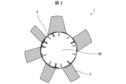
- FIG. 2 is a cross-sectional view showing an example of the configuration of the quantum dot adduct shown in FIG. 1.
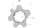
- FIG. 2 is a cross-sectional view showing another example of the configuration of the quantum dot adduct shown in FIG. 1 .
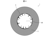
- FIG. 2 is a cross-sectional view showing another example of the configuration of the quantum dot adduct shown in FIG. 1 .
- FIG. 2 is a cross-sectional view showing another example of the configuration of the quantum dot adduct shown in FIG. 1 .
- FIG. 2 is a cross-sectional view showing another example of the configuration of the quantum dot adduct shown in FIG. 1 .
- FIG. 1 is a cross-sectional view showing an example of a configuration of a light-emitting element according to an embodiment of the disclosure.
- FIG. 2 is a cross
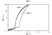
- FIG. 1 is a graph showing voltage-luminance characteristics of light-emitting elements according to Example 1 and Comparative Example 1.
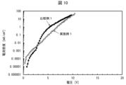
- FIG. 2 is a graph showing voltage-current density characteristics of light-emitting elements according to Example 1 and Comparative Example 1.
- FIG. 1 is a graph showing current density-luminance characteristics of light-emitting elements according to Example 1 and Comparative Example 1.
- FIG. 1 is a graph showing the current density-EQE characteristics of light-emitting elements according to Example 1 and Comparative Example 1.
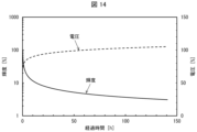
- FIG. 13 is a graph showing the emission luminance and driving voltage of the light-emitting element according to Example 1 over time in a constant current test.
- FIG. 13 is a graph showing the emission luminance and driving voltage over time of a light-emitting element according to Comparative Example 1 in a constant current test.
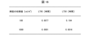
- FIG. 11 is a diagram showing an estimated value of the useful life of the light-emitting element according to the first embodiment.
- 13 is a diagram showing an estimated value of the useful life of a light-emitting element according to Comparative Example 1.
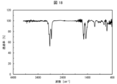
- FIG. FIG. 1 shows the results of FTIR of a solution of a quantum dot adduct according to Example 1.
- FIG. 1 is a diagram showing the results of FTIR of a quantum dot solution according to Comparative Example 1.
- 1 is a cross-sectional view illustrating an example of a configuration of a
- Fig. 1 is a cross-sectional view showing an example of the configuration of a light-emitting element according to an embodiment of the present disclosure.
- the light-emitting element 10 according to the present disclosure includes a first electrode 12 and a second electrode 16 facing each other, and a light-emitting layer 14 provided between the first electrode 12 and the second electrode 16, and includes quantum dots QD and an additive 2 located at least partially around the quantum dots QD, and the additive 2 is at least one of a discontinuous film, a non-uniform thickness, a porous material, and a portion having a thickness of 1 nm or less.
- the quantum dots QD and the additive 2 constitute a quantum dot additive 1.
- the additive 2 does not impede carrier injection into the quantum dots QD. Therefore, the efficiency of carrier injection into the quantum dots QD in the light-emitting element 10 can be improved, and the light-emitting efficiency of the light-emitting element 10 can be improved.
- the light-emitting element 10 may include additional components, such as one or more of a substrate 11 on which the first electrode 12 is formed, a sealing film 17 covering the second electrode 16, a charge transport layer 13 located between the first electrode 12 and the light-emitting layer 14, and a charge transport layer 15 located between the second electrode 16 and the light-emitting layer 14.
- the appendage 2 is in direct contact with the quantum dot QD. This means that the outside of the appendage 2 is close to the quantum dot QD, improving the efficiency of carrier injection into the quantum dot QD.
- the band gap of the additive 2 is wider than the band gap of the constituent material of the quantum dot QD.
- the band gap of the additive 2 is wider than the band gap of the constituent material of the shell.
- the additive 2 is insulating.
- the additive 2 may be inorganic.
- the additive 2 may, for example, comprise silicon oxide (SiO 2 ) and may further comprise silicic acid ([SiO x (OH) 4-2x ] n ).
- the additive 2 may comprise titanium oxide (TiO 2 ).
- the additive 2 may comprise aluminum oxide (Al 2 O 3 ).
- the additive 2 may comprise zinc chloride (ZnCl 2 ).
- the additive 2 may comprise silicon nitride (Si 3 N 4 ).
- the additive 2 may include, for example, one or more selected from the group consisting of boron oxide (B 2 O 3 ), phosphorus oxide (P 2 O 5 ), germanium oxide (GeO 2 ), beryllium fluoride (BeF 2 ), arsenic sulfide (As 2 S 3 ), silicon selenide (SiSe 2 ), germanium sulfide (GeS), tellurium oxide (TeO 2 ), bismuth oxide (Bi 2 O 3 ), vanadium oxide (V 2 O 5 ), antimony oxide (Sb 2 O 5 ), lead oxide (PbO), copper oxide (CuO), zirconium fluoride (ZrF 4 ), aluminum fluoride (AlF 3 ), indium fluoride (InF 3 ), and zinc bromide (ZnBr 2 ).
- B 2 O 3 boron oxide
- P 2 O 5 germanium oxide
- GeO 2 germanium oxide
- BeF 2 beryllium fluoride
- Additional material 2 may include at least one of polycrystalline and amorphous.
- the maximum thickness of additive material 2 may be 2 nm or more.
- FIG. 2 is a cross-sectional view showing an example of the configuration of the quantum dot adduct shown in FIG. 1.
- the adduct 2 may be solid and may include a discontinuous film arranged around the quantum dot QD in a cross section passing through the quantum dot QD.
- the discontinuous film has one or more discontinuous points in the circumferential direction centered on the quantum dot.
- Solid may mean that there is no region in which the constituent elements of the adduct 2 are missing or that the region is negligibly small, and typically means that the size of the missing region is 5 [nm] or less.
- the "discontinuous point” may be a region in which one or more types of constituent elements of the adduct 2 are missing, and typically has a size of more than 8 [nm]. The discontinuous point may penetrate the adduct 2 three-dimensionally.
- the discontinuous point may include a gap between the multiple parts.
- a “solid discontinuous film” may mean a film that has discontinuities and is solid in the areas other than the discontinuities.
- “surrounding” refers to the area extending around an object (here, quantum dots QDs), and the distance from the object is not particularly limited. However, “surrounding” may be an area extending outward from the surface of an object to a given width, or may refer to an area from the quantum dots QDs having a width approximately equal to or less than the distance between adjacent quantum dots QDs.
- “disposed around” does not necessarily mean surrounding an object continuously, but also includes cases where the object is surrounded discontinuously, and cases where the area is disposed in only a part of the area extending around the object.
- FIG. 3 is a cross-sectional view showing another example of the configuration of the quantum dot adduct shown in FIG. 1.
- the adduct 2 may be solid and may include a continuous film of non-uniform thickness surrounding the quantum dot QD in a cross section passing through the quantum dot QD.
- the thickness of the adduct 2 is the size in the radial direction centered on the quantum dot QD. With this configuration, the adduct 2 protects the quantum dot QD, and carriers can be injected into the quantum dot QD through the thin part of the adduct 2.
- the minimum thickness of the adduct 2 may be 1 nm or less.
- the film thickness of the continuous film may be 1 nm or less as a whole, and carriers can be injected into the quantum dot QD more efficiently.
- the film thickness of the continuous film may be a uniform continuous film with a film thickness of 1 nm or less as a whole.
- FIG. 4 is a cross-sectional view showing another example of the configuration of the quantum dot adduct shown in FIG. 1.
- the adduct 2 may be porous and may include a continuous film surrounding the quantum dot QD in a cross section passing through the quantum dot QD.
- the adduct 2 protects the quantum dot QD, and carriers can be injected into the quantum dot QD through the pores of the adduct 2.
- the porous pores may be regions in which one or more of the constituent elements of the adduct 2 are missing, and typically have a size of more than 5 nm and not more than 8 nm. The pores may penetrate the adduct 2 three-dimensionally.
- FIG. 5 is a cross-sectional view showing another example of the configuration of the quantum dot adduct shown in FIG. 1.
- the adduct 2 may be porous and may include a discontinuous film disposed around the quantum dot QD in a cross section passing through the quantum dot QD. With this configuration, the adduct 2 protects the quantum dot QD, and carriers can be injected into the quantum dot QD through discontinuities or pores in the adduct 2.
- a "porous discontinuous film” may mean a film having discontinuities and having porous areas other than the discontinuities.
- FIG. 6 is a cross-sectional view showing another example of the configuration of the quantum dot adduct shown in FIG. 1.
- the adduct 2 may be porous and may include a continuous film of non-uniform thickness surrounding the quantum dot QD in a cross section passing through the quantum dot QD. With this configuration, the adduct 2 protects the quantum dot QD, and carriers can be injected into the quantum dot QD through the pores or thin parts of the adduct 2.
- the minimum thickness of the adduct 2 may be 1 nm or less.
- the quantum dot adduct 1 includes a quantum dot QD and an adduct 2 located at least partially around the quantum dot QD, and the adduct 2 is at least one of a discontinuous film, an uneven thickness, a porous film, and a film having a portion with a thickness of 1 nm or less.
- the quantum dot adduct 1 may further include an element 6 for passivating surface defects of the quantum dot QD.
- the element 6 may be a halogen.
- the manufacturing method of the light-emitting element 10 may be any manufacturing method, and the light-emitting element 10 may be manufactured using general materials and general film-forming and sealing processes.
- an alcohol solution in which the quantum dot adduct 1 is dispersed may be applied by a spin coating method, a slit coating method, or the like to form a film of the light-emitting layer 14.
- the quantum dot adduct 1 may be mixed with a solvent for viscosity control, and an ink containing the quantum dot adduct 1 may be printed by an inkjet method, a screen printing method, or the like to form a film of the light-emitting layer 14.
- the printing method is suitable for producing a light-emitting panel and a display panel because it can uniformly form a film of the light-emitting layer 14 over a large area.
- Example 1 A quantum dot adduct 1 and a light-emitting element 10 according to an embodiment of the present disclosure will be described below.
- a commercially available red quantum dot was prepared as the quantum dot QD, an ethanol (C 2 H 6 O) solution of 0.02 [mol/L] zinc chloride (ZnCl 2 ) was prepared as a halogen source, and tetramethyl orthosilicate (TMOS) was prepared as a precursor of the adduct 2.
- the red quantum dot had a core of ZeSeTe, a shell of ZeS, and was coordinated with an organic ligand.
- the following chemical formula (1) shows TMOS.
- Octane (C 8 H 18 ) and N-methylformamide (NMF) were prepared as solvents.
- FIG. 7 and 8 are diagrams showing a method for producing a quantum dot adduct according to an embodiment of the present disclosure.
- a zinc chloride ethanol solution was mixed with the first liquid L1 in which quantum dots QDs were dispersed in octane, and the mixture was kept at room temperature for about 1 hour.
- stirring may be performed using a stirrer or the like.
- This process causes chlorine to inactivate the defects (not inactivated by the ligand) remaining on the surface of the quantum dots QDs.
- active defects are indicated by crosses, and inactivated defects or chlorine that has entered the defects are indicated by circles.
- chlorine was coordinated to the quantum dots QDs in addition to the organic ligands described above.
- the first liquid L1 may be used as it is in the subsequent process, or the first liquid L1 may be centrifuged to separate the quantum dots QDs to which the organic ligands and chlorine are coordinated, and the quantum dots QDs may be dispersed again in pure octane and used in the subsequent process as new first liquid L1.
- a second liquid L2 in which TMOS was dissolved in NMF was prepared.
- the quantum dots QD were coordinated with the above-mentioned organic ligands.
- the concentration of TMOS in the second liquid L2 was 0.02 [mol/L].
- the first liquid L1 and the second liquid L2 were thoroughly stirred and mixed.
- the quantum dots QDs were also coordinated with the halogen, and some of the defects in the quantum dots QDs were inactivated.
- the quantum dots QDs were transferred from the first liquid L1 to the second liquid L2.
- the quantum dot adduct 1 was formed in the second liquid L2.
- TMOS reacted to synthesize silicon oxide. Since the reaction was performed at around room temperature, the crystal system of the silicon oxide was trigonal. The crystal systems of the ZeS shell of the quantum dot QD and the silicon oxide are different, and the lattice constants are significantly different. Therefore, a large lattice mismatch occurs between the ZeS shell of the quantum dot QD and the silicon oxide grown thereon. The melting point of silicon oxide is 1710°C.
- the inorganic film containing silicon oxide and silicic acid was placed at least partially around the quantum dot QD.
- the solvent was replaced with alcohol. Specifically, the first liquid L1 was removed, and ethyl acetate was added to the second liquid L2 to precipitate and separate the quantum dot adduct 1.
- the quantum dot adduct 1 was then dispersed in ethanol.
- Other alcohols such as methanol and IPA may be used instead of ethanol.
- the alcohol can remove water (H 2 O) from silicon oxide and silicic acid, and prevent the water from corroding the quantum dots QD.
- quantum dot adduct 1 was again precipitated and separated with ethyl acetate, and dispersed in alcohol. Since silicon oxide and silicic acid tend to retain water, it is desirable to repeat alcohol dehydration multiple times. In this example, alcohol dehydration was performed twice.
- quantum dot adduct according to Example 1 refers to quantum dot adduct 1 after the second alcohol dehydration.
- the quantum dot adduct 1 according to Example 1 was used to manufacture the light-emitting element 10 according to Example 1, and the element characteristics and service life of the light-emitting element 10 were measured.
- the solution of the quantum dot adduct 1 according to Example 1 was analyzed by Fourier transform infrared spectroscopy (FTIR).
- Comparative Example 1 In Comparative Example 1, the commercially available red quantum dots described above were used as they were instead of the quantum dot adduct 1, and otherwise a light-emitting device according to Comparative Example 1 was manufactured in the same manner as the light-emitting device 10 according to Example 1, and the device characteristics and service life were measured. In addition, the commercially available red quantum dots were analyzed by Fourier transform infrared spectroscopy (FTIR). Hereinafter, the "quantum dots according to Comparative Example 1" refers to the commercially available red quantum dots.
- FTIR Fourier transform infrared spectroscopy
- FIGS. 9 to 12 are graphs showing the element characteristics (voltage-luminance characteristics, voltage-current density characteristics, current density-luminance characteristics, and current density-luminous efficiency characteristics) of the light-emitting elements according to Example 1 and Comparative Example 1, respectively.
- the points for Example 1 and Comparative Example 1 are shown as triangles and circles, respectively, and the points are connected by solid lines.
- the light-emitting device of Example 1 has a turn-on voltage in the luminance-voltage characteristics (see Figure 9) that is only about 2 V higher. Also, as with Comparative Example 1, the luminance of the light-emitting device of Example 1 increases with increasing voltage at voltages higher than the turn-on voltage. This result is thought to indicate that in Example 1, the addition 2 protecting the quantum dots QDs is at least one of a discontinuous film, an uneven thickness, a porous material, and a material having a portion with a thickness of 1 nm or less, and therefore no excessive voltage is required for carrier transport to the QDs.
- FIG. 13 and 14 are graphs showing the luminance and driving voltage of the light-emitting elements according to Example 1 and Comparative Example 1 over time in a constant current test.
- the horizontal axis of each figure shows the time from the start of light emission.
- the vertical axis on the left side shows the relative luminance when the luminance of each light-emitting element at the start of light emission is set to 100%.
- the vertical axis on the right side shows the relative voltage when the driving voltage of each light-emitting element at the start of light emission is set to 100%.
- the relationship between luminance and time is shown by a solid line, and the relationship between voltage and time is shown by a dashed line.
- the light-emitting element according to Example 1 exhibited a characteristic in which the luminance increased from the start until about 91 hours (so-called "positive aging”).
- the positive aging time was the elapsed time when the time derivative of the luminance was approximated by least squares and the sign changed from positive (positive aging) to negative (deterioration). This is considered to be an improvement in the EQE according to Example 1 by energization.
- the luminance increased from about 341 [cd/m 2 ] at the start of light emission to about 390 [cd/m 2 ] after about 91 hours, which is a large improvement of about 1.14 times, from the initial 8% to 9% in terms of EQE.
- the light extraction efficiency of the light-emitting element is determined by the refractive index of each material, and since the light extraction efficiency of a light-emitting element using a glass substrate, a general organic carrier transport material, a metal oxide, etc. does not exceed 20%, the IQE (internal quantum efficiency) after 26 hours of energization in the light-emitting element according to Example 1 exceeds 45%.
- This positive aging is a phenomenon specific to Example 1, and is believed to be the result of additive 2 gradually inactivating the surface defects of the quantum dots QDs through electrochemical reactions, electrophoresis, etc.
- the light-emitting element according to Comparative Example 1 does not show positive aging, and the luminance rapidly and monotonically decreases with the passage of current.
- the luminance decreases from about 157 [cd/ m2 ] at the start of emission to about 13 [cd/ m2 ] after about 20 hours, which is about 1/12 of the original luminance.
- This is considered to be the result of the quantum dots according to Comparative Example 1 being only protected by the organic ligand, and therefore rapidly deteriorating due to the passage of current.
- the deterioration may include the deterioration of the organic ligand itself, or the dissociation of the organic ligand from the quantum dot. Since the deterioration is rapid, it is considered difficult to use the quantum dots in a display panel or the like.
- 15 and 16 are diagrams showing estimated values of useful life of light-emitting elements according to Example 1 and Comparative Example 1, respectively.
- the following relational expression is established for the lifetime LT (x,P) until the emission luminance reaches x [%] of the initial value when the initial value of the emission luminance is L0 (P), and the lifetime LT(x,Q) until the emission luminance reaches x [%] of the initial value when the initial value of the emission luminance is L0 (Q), regardless of L0(P), L0 (Q), and x.
- the following relational expression is called the "reliability calculation formula".
- Example 1 when the initial luminance is 100 [cd/ m2 ], the L50 of Comparative Example 1 is about 0.1 hours, whereas the LT50 of Example 1 is about 380,000 hours, which is more than one million times as reliable. Therefore, according to Example 1, the efficiency of carrier injection into the quantum dots QD can be improved, and a light-emitting element 10 with a high EQE and a long service life can be realized.
- Non-Patent Document 1 the quantum dots are completely covered with a dense continuous film of silicon oxide. Compared to light-emitting devices using quantum dots that are only protected with organic ligands, Non-Patent Document 1 shows that reliability is improved, but only by about three times. In the light-emitting device containing quantum dots described in Non-Patent Document 1, there is only a small amount of organic ligand inside the continuous film, and the continuous film is not in direct contact with the quantum dots, so it is thought that positive aging due to current flow does not occur. In addition, since the carrier injection into the quantum dots in Non-Patent Document 1 is via the ⁇ electrons of the organic cyclic molecules mixed in the silicon oxide, it is speculated that the carriers actually injected into the quantum dots are insufficient. Furthermore, since the carrier injection into the quantum dots in Non-Patent Document 1 is via organic molecules, it is speculated that even cyclic molecules cannot reduce deterioration due to electrochemical reactions.
- FIG. 17 and 18 are diagrams showing the results of FTIR (Fourier transform infrared spectroscopy) of the quantum dot adduct according to Example 1 and the quantum dot solution according to Comparative Example 1, respectively.
- FTIR Fastier transform infrared spectroscopy
- FIG. 18 in Comparative Example 1, only a peak corresponding to the C-H bond of the organic ligand is observed.
- FIG. 17 in Example 1, in addition to the peak corresponding to the C-H bond, a peak corresponding to the Si-O bond of silicon dioxide is observed at 1000 to 1200 [cm ⁇ 1 ], and a broad peak corresponding to the Si-OH bond of silicic acid is observed at 2600 to 3600 [cm ⁇ 1 ].
- Example 1 the quantum dots in Example 1 are protected by an inorganic film containing silicon dioxide and silicic acid, and the quantum dots in Comparative Example 1 are not protected by an inorganic film.
- the "peak corresponding to the . . . bond” will be referred to as the ". . . peak”.
- Silicon oxide naturally (i.e., when only silicon oxide is produced) forms a dense and continuous inorganic film.
- Silicic acid is insoluble in acid and inhibits the synthesis of silicon oxide. Therefore, an appropriate amount of silicic acid helps the formation of an inorganic film containing silicon oxide and silicic acid so that the inorganic film is at least one of the following: a discontinuous film, an uneven thickness, a porous film, and a film having a thickness of 1 nm or less.
- excess silicic acid forms a dense and continuous film together with silicon dioxide, covering the quantum dots QDs.
- silicic acid plays an important role in protecting and insulating the quantum dots QDs.
- the amount of silicic acid produced can be adjusted by the amount of TMOS.
- the amount of silicic acid is appropriate, and it is presumed that the inorganic film containing silicon oxide and silicic acid is at least one of the following: it is a discontinuous film, it is non-uniform in thickness, it is porous, or it has a portion with a thickness of 1 nm or less.
- silicon oxide is unlikely to form a continuous film on the quantum dot adduct 1.
- One of the two conditions is that the TMOS is less than 0.02 mol/L.
- the other is that silicon oxide is synthesized at a low temperature below room temperature.
- Non-Patent Document 1 the results of FTIR are shown only in the range of about 800 to 3200 [cm ⁇ 1 ], but it is considered that the material in Non-Patent Document 1 does not contain silicic acid, judging from the slope of the spectrum in the vicinity of 3200 [cm ⁇ 1 ]. Furthermore, in Non-Patent Document 1, the quantum dots are protected with silicon dioxide, and the intensity of the C-H peak is about the same as the intensity of the Si-O peak, which indicates cyclic organic molecules that contribute to carrier injection into the quantum dots.
- Example 1 of the present disclosure the intensity of the C-H peak is less than one-tenth of the Si-O peak, and in Comparative Example 2, the intensity of the C-H peak is less than one-half of the Si-O peak. Therefore, it is considered that the inorganic films in Example 1 and Comparative Example 2 do not contain organic cyclic structures or contain only trace amounts, and that cyclic organic molecules do not contribute to carrier injection into the quantum dots. In particular, the C-H peak in Example 1 is very weak, which is completely different from Non-Patent Document 1.
- FIG. 19 is a cross-sectional view showing an example of the configuration of a display device according to an embodiment of the present disclosure.
- a display device 100 according to the present disclosure includes a light-emitting device 10 according to an embodiment of the present disclosure.
- the light-emitting device 10 may be the light-emitting device 10 described in the above-mentioned embodiment 1, or a light-emitting device obtained by improving or modifying the light-emitting device 10 described in the above-mentioned embodiment 1.
- the display device 100 may include a display unit 30 including a plurality of sub-pixels X, and a driver circuit 25 that drives the plurality of sub-pixels X. At least one of the plurality of sub-pixels X may include a light-emitting element 10 and a pixel circuit 20.
Landscapes
- Chemical & Material Sciences (AREA)
- Engineering & Computer Science (AREA)
- Crystallography & Structural Chemistry (AREA)
- Inorganic Chemistry (AREA)
- Nanotechnology (AREA)
- Physics & Mathematics (AREA)
- Optics & Photonics (AREA)
- Electroluminescent Light Sources (AREA)
Abstract
本開示に係る発光素子(10)は、第1電極(12)および第2電極(16)の間に設けられた発光層(14)であり、量子ドット(QD)と、量子ドット(QD)の周囲の少なくとも一部に位置する付加物(2)とを含み、付加物(2)は、不連続膜であるか、厚さが不均一であるか、多孔質であるか、厚さが1〔nm〕以下の部分を有するかの少なくとも何れか1つである発光層を備える。
Description
本開示は、発光素子、表示装置、および量子ドット付加体に関する。
耐久性向上のために、量子ドットをシリカ(酸化シリコン)で覆う研究がおこなわれている。非特許文献1は、有機環状構造を導入したシリカで量子ドットを覆う構成を開示している。
「Blue-Emitting InP/GaP/ZnS Quantum Dots with Enhanced Stability by Siloxane Capping: Implication for Electroluminescent Devices」(ACS Appl. Nano Mater . 2022, 5, 2801-2811)
シリカは絶縁性であるため、量子ドットをシリカで覆うことによって、量子ドットへのキャリア注入が阻害される問題がある。非特許文献1は、有機環状構造をシリカに導入して、π電子によるキャリア注入効率の向上を試みたが、しかし、依然としてキャリア注入が不十分である。
本開示の一態様に係る発光素子は、対向する第1電極および第2電極と、前記第1電極および前記第2電極との間に設けられた発光層であり、量子ドットと、前記量子ドットの周囲の少なくとも一部に位置する付加物とを含み、前記付加物は、不連続膜であるか、厚さが不均一であるか、多孔質であるか、厚さが1〔nm〕以下の部分を有するかの少なくとも何れか1つである発光層と、を備える構成である。
本開示の一態様に係る量子ドット付加体は、量子ドットと、前記量子ドットの周囲の少なくとも一部に位置する付加物とを含み、前記付加物は、不連続膜であるか、厚さが不均一であるか、多孔質であるか、厚さが1〔nm〕以下の部分を有するかの少なくとも何れか1つである、構成である。
本開示の一態様に係る構成によれば、量子ドットへのキャリア注入効率を向上できる。
〔実施形態1〕
(発光素子の構成)
図1は、本開示の一実施形態に係る発光素子の構成の一例を示す断面図である。図1に示すように、本開示に係る発光素子10は、互いに対向する第1電極12および第2電極16と、第1電極12および第2電極16との間に設けられた発光層14であり、量子ドットQDと、量子ドットQDの周囲の少なくとも一部に位置する付加物2とを含み、付加物2は、不連続膜であるか、厚さが不均一であるか、多孔質であるか、厚さが1〔nm〕以下の部分を有するかの少なくとも何れか1つである発光層14と、を備える。量子ドットQDと付加物2とが、量子ドット付加体1を構成している。
(発光素子の構成)
図1は、本開示の一実施形態に係る発光素子の構成の一例を示す断面図である。図1に示すように、本開示に係る発光素子10は、互いに対向する第1電極12および第2電極16と、第1電極12および第2電極16との間に設けられた発光層14であり、量子ドットQDと、量子ドットQDの周囲の少なくとも一部に位置する付加物2とを含み、付加物2は、不連続膜であるか、厚さが不均一であるか、多孔質であるか、厚さが1〔nm〕以下の部分を有するかの少なくとも何れか1つである発光層14と、を備える。量子ドットQDと付加物2とが、量子ドット付加体1を構成している。
この構成によれば、量子ドットの周囲を覆う付加物が連続膜かつ厚さ均一かつ密実である従来構成と比較して、付加物2が量子ドットQDへのキャリア注入を阻害しない。そのため、発光素子10における量子ドットQDへのキャリア注入効率を向上でき、発光素子10の発光効率を向上できる。
第1電極12および第2電極16の何れか一方がアノードであり、他方がカソードである。第1電極12および第2電極16の少なくとも一方は透明電極である。発光素子10は追加的構成要素を備えてよく、例えば、第1電極12がその上に形成されている基板11、第2電極16を覆う封止膜17、第1電極12と発光層14との間に位置する電荷輸送層13、および、第2電極16と発光層14との間に位置する電荷輸送層15の何れか1つ以上を備えてよい。
付加物2は、量子ドットQDと直接接している。このため、付加物2の外側から量子ドットQDまでが近く、量子ドットQDへのキャリア注入効率を向上できる。
付加物2のバンドギャップは、量子ドットQDの構成材料のバンドギャップよりも広い。量子ドットQDがコアとコアを囲むシェルとを有する場合、付加物2のバンドギャップは、シェルの構成材料のバンドギャップよりも広い。通常、付加物2は絶縁性である。
付加物2は無機物であってよい。付加物2は例えば、酸化シリコン(SiO2)を含んでよく、さらにケイ酸([SiOx(OH)4-2x]n)を含んでよい。付加物2は、酸化チタン(TiO2)を含んでよい。付加物2は、酸化アルミニウム(Al2O3)を含んでよい。付加物2は、塩化亜鉛(ZnCl2)を含んでよい。付加物2は、窒化シリコン(Si3N4)を含んでよい。付加物2は例えば、酸化ホウ素(B2O3)、酸化リン(P2O5)、酸化ゲルマニウム(GeO2)、フッ化ベリリウム(BeF2)、硫化ヒ素(As2S3)、セレン化シリコン(SiSe2)、硫化ゲルマニウム(GeS)、酸化テルル(TeO2)、酸化ビスマス(Bi2O3)、酸化バナジウム(V2O5)、酸化アンチモン(Sb2O5)、酸化鉛(PbO)、酸化銅(CuO)、フッ化ジルコニウム(ZrF4)、フッ化アルミニウム(AlF3)、フッ化インジウム(InF3)、および臭化亜鉛(ZnBr2)から成る群から選択された1つ以上を含んでよい。なお、化合物名の後に括弧で記載した化学式は代表的な例示である。また、化学式に記載の組成比はストイキオメトリであればよいが、必ずしもストイキオメトリでなくてもよい。
付加物2は、多結晶およびアモルファスの少なくとも一方を含んでよい。付加物2の最大厚さは、2〔nm〕以上であってよい。
(量子ドット付加体の構成)
図2は、図1に示した量子ドット付加体の構成の一例を示す断面図である。図2に示すように、付加物2は、密実であってよく、量子ドットQDを通る一断面において量子ドットQDの周囲に配置された不連続膜を含んでよい。不連続膜は、量子ドットを中心とする周方向に1つ以上の不連続点を有する。この構成によれば、付加物2が量子ドットQDを保護すると共に、付加物2の不連続点を通って、キャリアが量子ドットQDに注入されることができる。「密実」は、付加物2の構成元素が欠損している領域が無いか、あるいは無視できるほど小さいことを意味してよく、典型的には、欠損している領域のサイズが5〔nm〕以下であることを意味してよい。「不連続点」は、付加物2の構成元素の1種類以上が欠損している領域であってよく、典型的には、8〔nm〕超のサイズを有する。不連続点は、三次元的に付加物2を貫通していてよい。また、1個の量子ドットに対する付加物2が、互いと分離独立している複数の部分から成る場合、不連続点は、複数の部分の間の隙間を含んでよい。「密実な不連続膜」は、不連続点を有し、不連続点以外の領域が密実である膜を意味してよい。
図2は、図1に示した量子ドット付加体の構成の一例を示す断面図である。図2に示すように、付加物2は、密実であってよく、量子ドットQDを通る一断面において量子ドットQDの周囲に配置された不連続膜を含んでよい。不連続膜は、量子ドットを中心とする周方向に1つ以上の不連続点を有する。この構成によれば、付加物2が量子ドットQDを保護すると共に、付加物2の不連続点を通って、キャリアが量子ドットQDに注入されることができる。「密実」は、付加物2の構成元素が欠損している領域が無いか、あるいは無視できるほど小さいことを意味してよく、典型的には、欠損している領域のサイズが5〔nm〕以下であることを意味してよい。「不連続点」は、付加物2の構成元素の1種類以上が欠損している領域であってよく、典型的には、8〔nm〕超のサイズを有する。不連続点は、三次元的に付加物2を貫通していてよい。また、1個の量子ドットに対する付加物2が、互いと分離独立している複数の部分から成る場合、不連続点は、複数の部分の間の隙間を含んでよい。「密実な不連続膜」は、不連続点を有し、不連続点以外の領域が密実である膜を意味してよい。
また、「周囲」は、物(ここでは量子ドットQD)の周囲に広がる領域を意味し、物からの距離は特に限定するものではない。ただし、「周囲」は、物の表面から外側に所与の幅に広がる領域であってよく、おおよそ隣接する量子ドットQD間の距離以内の幅をもつ量子ドットQDからの領域を意味してもよい。また「周囲に配置された」は、物を連続的に囲むことを必ずしも意味するものではなく、物を断続的に囲む場合、および、物の周囲に広がる領域の一部だけに配置される場合も含む。
図3は、図1に示した量子ドット付加体の構成の別の一例を示す断面図である。図3に示すように、付加物2は、密実であってよく、量子ドットQDを通る一断面において量子ドットQDを囲む、厚さが不均一な連続膜を含んでよい。付加物2の厚さは、量子ドットQDを中心とする放射方向のサイズである。この構成によれば、付加物2が量子ドットQDを保護すると共に、付加物2の薄い部分を通って、キャリアが量子ドットQDに注入されることができる。付加物2の最小厚さは、1〔nm〕以下であってよい。1〔nm〕以下とすることにより、薄い部分をさらに効率的にキャリアが通過でき、効率的にキャリアが量子ドットQDに注入されることができる。また、連続膜の膜厚は全体が、1〔nm〕以下の膜厚となっていてもよく、さらに効率的にキャリアが量子ドットQDに注入されることができる。なお、全体が1〔nm〕以下の膜厚で均一の連続膜であってもよい。
図4は、図1に示した量子ドット付加体の構成の別の一例を示す断面図である。図4に示すように、付加物2は多孔質であってよく、量子ドットQDを通る一断面において量子ドットQDを囲む連続膜を含んでよい。この構成によれば、付加物2が量子ドットQDを保護すると共に、付加物2の細孔を通って、キャリアが量子ドットQDに注入されることができる。多孔質の細孔は、付加物2の構成元素の1種類以上が欠損している領域であってよく、典型的には、5〔nm〕超8〔nm〕以下のサイズを有する。細孔は、三次元的に付加物2を貫通していてよい。
図5は、図1に示した量子ドット付加体の構成の別の一例を示す断面図である。図5に示すように、付加物2は多孔質であってよく、量子ドットQDを通る一断面において量子ドットQDの周囲に配置された不連続膜を含んでよい。この構成によれば、付加物2が量子ドットQDを保護すると共に、付加物2の不連続点または細孔を通って、キャリアが量子ドットQDに注入されることができる。「多孔質な不連続膜」は、不連続点を有し、不連続点以外の領域が多孔質である膜を意味してよい。
図6は、図1に示した量子ドット付加体の構成の別の一例を示す断面図である。図6に示すように、付加物2は多孔質であってよく、量子ドットQDを通る一断面において量子ドットQDを囲む、厚さが不均一な連続膜を含んでよい。この構成によれば、付加物2が量子ドットQDを保護すると共に、付加物2の細孔または付加物2の薄い部分を通って、キャリアが量子ドットQDに注入されることができる。付加物2の最小厚さは、1〔nm〕以下であってよい。
図2~図6に示すように、本開示に係る量子ドット付加体1は、量子ドットQDと、量子ドットQDの周囲の少なくとも一部に位置する付加物2とを含み、付加物2は、不連続膜であるか、厚さが不均一であるか、多孔質であるか、厚さが1〔nm〕以下の部分を有するかの少なくとも何れか1つである。量子ドット付加体1はさらに、量子ドットQDの表面欠陥を不活性化するための元素6を含んでよい。元素6はハロゲンであってよい。
(製造方法)
本開示に係る発光素子10の製造方法は、任意の製造方法であってよく、一般的な材料と一般的な成膜及び封止工程によって発光素子10を製造してよい。例えば、量子ドット付加体1が分散しているアルコール溶液をスピンコート法またはスリットコート法などによって塗布し、発光層14を成膜できる。例えば、量子ドット付加体1を粘性制御のための溶媒と混合し、量子ドット付加体1を含むインクをインクジェット法またはスクリーン印刷法などによって印刷し、発光層14を成膜できる。印刷法は、大面積に発光層14を均一に成膜できるため、発光パネルおよび表示パネルの作成に適する。
本開示に係る発光素子10の製造方法は、任意の製造方法であってよく、一般的な材料と一般的な成膜及び封止工程によって発光素子10を製造してよい。例えば、量子ドット付加体1が分散しているアルコール溶液をスピンコート法またはスリットコート法などによって塗布し、発光層14を成膜できる。例えば、量子ドット付加体1を粘性制御のための溶媒と混合し、量子ドット付加体1を含むインクをインクジェット法またはスクリーン印刷法などによって印刷し、発光層14を成膜できる。印刷法は、大面積に発光層14を均一に成膜できるため、発光パネルおよび表示パネルの作成に適する。
(実施例1)
本開示の一実施例に係る量子ドット付加体1および発光素子10について、以下に説明する。量子ドットQDとして市販の赤色量子ドットを、ハロゲン源として塩化亜鉛(ZnCl2)0.02〔mol/L〕のエタノール(C2H6O)溶液を、付加物2の前駆体としてオルトケイ酸テトラメチル(TMOS)を用意した。赤色量子ドットは、コアがZeSeTeであり、シェルがZeSであり、有機リガンドが配位していた。下記の化学式(1)はTMOSを示す。また、溶媒として、オクタン(C8H18)とN-メチルホルムアミド(NMF)とを用意した。
本開示の一実施例に係る量子ドット付加体1および発光素子10について、以下に説明する。量子ドットQDとして市販の赤色量子ドットを、ハロゲン源として塩化亜鉛(ZnCl2)0.02〔mol/L〕のエタノール(C2H6O)溶液を、付加物2の前駆体としてオルトケイ酸テトラメチル(TMOS)を用意した。赤色量子ドットは、コアがZeSeTeであり、シェルがZeSであり、有機リガンドが配位していた。下記の化学式(1)はTMOSを示す。また、溶媒として、オクタン(C8H18)とN-メチルホルムアミド(NMF)とを用意した。

次いで図8に示すように、第1液L1と第2液L2とを十分に撹拌および混合した。撹拌過程で、ハロゲンも量子ドットQDが配位し、量子ドットQDの欠陥の一部を不活性化した。また、量子ドットQDが第1液L1から第2液L2に移行した。
第2液L2中で、量子ドット付加体1が形成された。TMOSが反応して、酸化シリコンが合成された。室温付近での反応であるため、酸化シリコンの結晶系は、三方晶である。量子ドットQDのシェルのZeSと酸化シリコンとの結晶系が異なり、格子定数が大きく異なる。したがって、量子ドットQDのシェルのZeSとその上に成長する酸化シリコンと間に、大きな格子不整合が生じる。また、酸化シリコンの融点は1710℃である。このため、量子ドットQDに接して、室温付近など1000℃超の融点に対して遥かに低温で合成された酸化シリコンは、単結晶には成長困難であり、多結晶、アモルファスまたは多孔質となり易い。加えて、一部のシリコン元素が水酸基(-OH)と結合して、かつ/または、一部の酸化シリコンが水(H2O)と反応して、ケイ酸が合成された。酸化シリコンおよびケイ酸を含む無機膜は、量子ドットQDの周囲の少なくとも一部に配置された。
続いて、溶媒をアルコールに置換した。具体的には、第1液L1を除去し、第2液L2に酢酸エチルを添加して、量子ドット付加体1を沈殿および分離した。そして、量子ドット付加体1をエタノール中に分散した。エタノールの代わりに、メタノールおよびIPAなど他のアルコールを用いてもよい。アルコールによって、酸化シリコンおよびケイ酸から水(H2O)を除去し、水が量子ドットQDを侵すことを防止できる。
再度、量子ドット付加体1を酢酸エチルによって沈殿および分離し、アルコール中に分散した。酸化シリコンおよびケイ酸は水を抱え易いので、アルコール脱水を複数回繰り返すことが望ましい。本実施例では、アルコール脱水を2回行った。以降、「実施例1に係る量子ドット付加体」は、2回目のアルコール脱水後の量子ドット付加体1を意味する。
次に、実施例1に係る量子ドット付加体1を用いて、実施例1に係る発光素子10を製造し、発光素子10の素子特性および耐用寿命を測定した。また、実施例1に係る量子ドット付加体1の溶液をフーリエ変換赤外線分光法(FTIR)によって分析した。
(比較例1)
比較例1では、量子ドット付加体1の代わりに前述の市販の赤色量子ドットをそのまま用いて、その他は実施例1に係る発光素子10と同様に、比較例1に係る発光素子を製造し、素子特性および耐用寿命を測定した。また、市販の赤色量子ドットをフーリエ変換赤外線分光法(FTIR)によって分析した。以降、「比較例1に係る量子ドット」は、市販の赤色量子ドットを意味する。
比較例1では、量子ドット付加体1の代わりに前述の市販の赤色量子ドットをそのまま用いて、その他は実施例1に係る発光素子10と同様に、比較例1に係る発光素子を製造し、素子特性および耐用寿命を測定した。また、市販の赤色量子ドットをフーリエ変換赤外線分光法(FTIR)によって分析した。以降、「比較例1に係る量子ドット」は、市販の赤色量子ドットを意味する。
図9~図12はそれぞれ、実施例1および比較例1に係る発光素子の素子特性(電圧-輝度特性、電圧-電流密度特性、電流密度-輝度特性、および電流密度-発光効率特性)のグラフを示す図である。各図において、実施例1および比較例1の点をそれぞれ、三角および丸で示し、点の間を実線で結ぶ。
図9~図12に示すように、比較例1と比較して、量子ドットQDが絶縁性の酸化シリコンに保護されているにも関わらず、実施例1に係る発光素子は、輝度-電圧特性(図9参照)における立ち上がり電圧が2V程度高いに過ぎない。また、比較例1と同様に、実施例1に係る発光素子の輝度は、立ち上がり電圧より高い電圧において電圧が大きくなるほど、大きい。この結果は、実施例1では、量子ドットQDを保護している付加物2が、不連続膜であるか、厚さが不均一であるか、多孔質であるか、厚さが1〔nm〕以下の部分を有するかの少なくとも何れか1つであるために、QDへのキャリア輸送に過剰な電圧が必要ないことを示していると考えられる。
図13および図14は、定電流試験における実施例1および比較例1に係る発光素子の時間経過に対する発光輝度および駆動電圧を示すグラフを示す図である。各図の横軸は、発光開始時からの時間を示す。左側縦軸は、発光開始時の各発光素子の発光輝度を100%とした相対輝度を示す。右側縦軸は、発光開始時の各発光素子の駆動電圧を100%とした相対電圧を示す。各図において、輝度と時間との関係を実線で示し、電圧と時間との関係を破線で示す。この定電流試験において、発光素子に25〔mA/cm2〕の電流を25℃で流した。また、この定電流試験における発光開始時の発光輝度は、実施例1に係る発光素子10で341〔cd/m2〕であり、比較例1に係る発光素子で157〔cd/m2〕であった。
図13に示すように、実施例1に係る発光素子は、開始時91時間程度まで輝度が上昇する特性(いわゆる「ポジティブエージング」)を示した。ここで、ポジティブエージングの時間は、輝度の時間微分を最小二乗近似してその符号が正(ポジティブエージング)から負(劣化)に転じる経過時間とした。これは、通電によって実施例1に係るEQEが向上していると考えられる。輝度は、発光開始時の約341〔cd/m2〕から約91時間経過後の約390〔cd/m2〕まで増大しており、約1.14倍、EQEに換算して初期の8%から9%まで大きく改善している。なお、発光素子の光取り出し効率は、各材料の屈折率で決まり、ガラス基板及び一般的な有機キャリア輸送材料、金属酸化物等を使った発光素子における光取り出し効率が20%を超えないことから、実施例1に係る発光素子において、26時間通電後のIQE(internal quantum efficiency)が45%を超えている。
このポジティブエージングは、実施例1に特有の現象であり、付加物2が電気化学反応や電気泳導などにより、量子ドットQDの表面欠陥を徐々に不活性化した結果と考えられる。
図14に示すように、比較例1に係る発光素子は、ポジティブエージングを示さず、通電時間とともに輝度が急速かつ単調に減少する。輝度は、発光開始時の約157〔cd/m2〕から約20時間経過後の約13〔cd/m2〕まで減少しており、約12分の1と劣化している。これは、比較例1に係る量子ドットは、有機リガンドで保護されただけであるため、通電によって劣化が急速に進行した結果と考えられる。劣化には、有機リガンド自体の劣化、または有機リガンドの量子ドットからの解離が含まれ得る。劣化が急速であるため、表示パネルなどへの実用は困難であると考えられる。
実施例1に係る輝度と時間との関係について、91時間から130時間までの測定値に、適用結果が片対数グラフで直線を描くように、最小二乗法によるフィッティング関数を適用した。本実施例の信頼性試験結果によれば、91時間までの領域で僅かなポジティブエージングが見られるため、時間に対して負の傾きで輝度が変化する91時間から130時間の間にフィッティング関数を適用した。比較例1に係る輝度と時間との関係について、20時間から130時間までの測定値に、適用結果が片対数グラフで直線を描くように、最小二乗法によるフィッティング関数を適用した。適用結果からそれぞれ、LT50およびLT95を算出した。「LT95」は、発光素子の発光輝度が初期値の95%になるまでの寿命時間(Lifetime)の推定値を示し、「LT50」は、発光素子の発光輝度が初期値の50%になるまでの寿命時間の推定値を示す。
図15および図16はそれぞれ、実施例1および比較例1に係る発光素子の耐用寿命の推定値を示す図である。一般的に、あるナノLEDにおいて、発光輝度の初期値がL0(P)のときに発光輝度が初期値のx〔%〕になるまでの寿命時間LT(x,P)と、発光輝度の初期値がL0(Q)のときに発光輝度が初期値のx〔%〕になるまでの寿命時間LT(x,Q)とに関し、L0(P)、L0(Q)、およびxに関わらず、下記の関係式が成立することが知られている。下記関係式は、「信頼性算出式」と呼ばれている。
LT(x、P)×{L0(P)}n=LT(x、Q)×{L0(Q)}n=定数
nは、ナノLEDに依存する係数であり、n=1.8であった。
nは、ナノLEDに依存する係数であり、n=1.8であった。
図15および図16に示すように、初期輝度が100〔cd/m2〕のときに、比較例1のL50が約0.1時間であるのに対し、実施例1のLT50が約380000時間と100万倍以上の信頼性が得られている。したがって、実施例1によれば、量子ドットQDへのキャリア注入効率を向上でき、EQEが高く耐用寿命が長い発光素子10を実現できた。
非特許文献1では、量子ドットの周囲を酸化シリコンの密実な連続膜で完全に覆う。有機リガンドで保護しているだけの量子ドットを用いた発光素子と比較して、非特許文献1によれば、信頼性が向上するが、3倍程度に過ぎない。非特許文献1に記載された量子ドットを含む発光素子では、連続膜の内側にある有機リガンドが僅かであるために、かつ、連続膜が量子ドットに直接接していないために、通電によるポジティブエージングが起きないと考えられる。また、非特許文献1における量子ドットへのキャリア注入は、酸化シリコン中に混合された有機環状分子のπ電子を介したキャリア注入であるため、量子ドットに実際に注入されたキャリアが不足すると推測される。さらに、非特許文献1における量子ドットへのキャリア注入は有機分子を介したキャリア注入であるため、環状分子であっても電気化学反応による劣化を低減できていないと推測される。
図17および図18はそれぞれ、実施例1に係る量子ドット付加体および比較例1に係る量子ドットの溶液のFTIR(フーリエ変換赤外線分光法)の結果を示す図である。図18に示すように、比較例1では、有機リガンドのC-H結合に対応するピークが観察されるに過ぎない。一方、図17に示すように、実施例1では、C-H結合に対応するピークに加えて、二酸化ケイ素のSi-O結合に対応するピークが1000~1200〔cm-1〕に観察され、ケイ酸のSi-OH結合に対応する幅広なピークが2600~3600〔cm-1〕に観察される。したがって、実施例1において量子ドットが二酸化ケイ素およびケイ酸を含む無機膜に保護されており、比較例1において量子ドットが無機膜に保護されていないことが分かる。以降、記載の簡単化のために、「……結合に対応するピーク」を「……ピーク」と称する。
酸化シリコンは本来(すなわち、酸化シリコンのみが生じる場合)、密実かつ連続な無機膜を構成する。ケイ酸は酸に不溶であり、酸化ケイ素の合成を阻害する。したがって、適量のケイ酸は、酸化シリコンおよびケイ酸を含む無機膜が、不連続膜であるか、厚さが不均一であるか、多孔質であるか、厚さが1〔nm〕以下の部分を有するかの少なくとも何れか1つであるように、無機膜の形成を助ける。一方、過剰なケイ酸は、二酸化ケイ素と共に密実な連続膜を形成し、量子ドットQDを覆う。このように、ケイ酸は量子ドットQDの保護および絶縁に重要な役割を担う。ケイ酸の生成量は、TMOSの量によって調整可能である。
実施例1は、ケイ酸が適量であり、酸化シリコンおよびケイ酸を含む無機膜が、不連続膜であるか、厚さが不均一であるか、多孔質であるか、厚さが1〔nm〕以下の部分を有するかの少なくとも何れか1つであると推定される。加えて、結晶系および格子定数が異なるという理由で、次の2つの条件の少なくとも一方を満たす場合に、酸化シリコンは量子ドット付加体1の上に連続膜を形成し難い。2つの条件のうちの1つは、TMOSが0.02〔mol/L〕未満であることである。もう1つは、室温以下の低温で酸化シリコンが合成されることである。
非特許文献1では、FTIRの結果が約800~3200〔cm-1〕の範囲で示されているに過ぎないが、3200〔cm-1〕近傍におけるスペクトルの傾きから推定して、非特許文献1の資料にはケイ酸は含まれていないと考えられる。さらに非特許文献1では、量子ドットを二酸化ケイ素で保護している資料で、C-Hピークの強度がSi-Oピークの強度と同程度であり、これは、量子ドットへのキャリア注入に寄与する環状有機分子を示している。対照的に、本開示の実施例1ではC-Hピークの強度がSi-Oピークの10分の1以下であり、比較例2ではC-Hピークの強度がSi-Oピークの2分の1以下である。したがって、実施例1および比較例2の無機膜に有機環状構造は含まれていないか、微量だけ含まれており、量子ドットへのキャリア注入に環状有機分子が寄与していないと考えられる。特に、実施例1ではC-Hピークが非常に弱く、非特許文献1と全く異なる。
〔実施形態2〕
本開示の他の実施形態について、以下に説明する。なお、説明の便宜上、上記実施形態にて説明した部材と同じ機能を有する部材については、同じ符号を付記し、その説明を繰り返さない。
本開示の他の実施形態について、以下に説明する。なお、説明の便宜上、上記実施形態にて説明した部材と同じ機能を有する部材については、同じ符号を付記し、その説明を繰り返さない。
図19は、本開示の一実施形態に係る表示装置の構成の一例を示す断面図である。図19に示すように、本開示に係る表示装置100は、本開示の一実施形態に係る発光素子10を備える。発光素子10は、前述の実施形態1に記載の発光素子10であっても、前述の実施形態1に記載の発光素子10に改良または変更を施した発光素子であってもよい。
表示装置100は、複数のサブ画素Xを含む表示部30と、複数のサブ画素Xを駆動するドライバ回路25とを備えてよい。複数のサブ画素Xの少なくとも1つが、発光素子10と画素回路20とを備えてよい。
本開示は上述した各実施形態に限定されるものではなく、請求項に示した範囲で種々の変更が可能であり、異なる実施形態にそれぞれ開示された技術的手段を適宜組み合わせて得られる実施形態についても本開示の技術的範囲に含まれる。
1 量子ドット付加体
2 付加物
10 発光素子
12 第1電極
14 発光層
16 第2電極
100 表示装置
QD 量子ドット
2 付加物
10 発光素子
12 第1電極
14 発光層
16 第2電極
100 表示装置
QD 量子ドット
Claims (22)
- 対向する第1電極および第2電極と、
前記第1電極および前記第2電極との間に設けられた発光層であり、量子ドットと、前記量子ドットの周囲の少なくとも一部に位置する付加物とを含み、前記付加物は、不連続膜であるか、厚さが不均一であるか、多孔質であるか、厚さが1〔nm〕以下の部分を有するかの少なくとも何れか1つである発光層と、
を備える発光素子。 - 前記付加物は、前記量子ドットと直接接している、請求項1に記載の発光素子。
- 前記付加物のバンドギャップは、前記量子ドットの構成材料のバンドギャップよりも広い、請求項1または2に記載の発光素子。
- 前記量子ドットは、コアと、コアを囲むシェルとを有し、
前記付加物のバンドギャップは、前記シェルの構成材料のバンドギャップよりも広い、請求項3に記載の発光素子。 - 前記付加物は、絶縁性である請求項3または4に記載の発光素子。
- 前記付加物は、酸化シリコンを含む請求項1~5の何れか1項に記載の発光素子。
- 前記付加物は、ケイ酸を含む請求項1~5の何れか1項に記載の発光素子。
- 前記付加物は、酸化チタンを含む請求項1~5の何れか1項に記載の発光素子。
- 前記付加物は、酸化アルミニウムを含む請求項1~5の何れか1項に記載の発光素子。
- 前記付加物は、塩化亜鉛を含む請求項1~5の何れか1項に記載の発光素子。
- 前記付加物は、窒化シリコンを含む請求項1~5の何れか1項に記載の発光素子。
- 前記付加物は、酸化ホウ素、酸化リン、酸化ゲルマニウム、フッ化ベリリウム、硫化ヒ素、セレン化シリコン、硫化ゲルマニウム、酸化テルル、酸化ビスマス、酸化バナジウム、酸化アンチモン、酸化鉛、酸化銅、フッ化ジルコニウム、フッ化アルミニウム、フッ化インジウム、および臭化亜鉛から成る群から選択された1つを含む請求項1~5の何れか1項に記載の発光素子。
- 前記付加物は、多結晶およびアモルファスの少なくとも一方を含む、請求項1~12の何れか1項に記載の発光素子。
- 前記付加物の最大厚さは、2〔nm〕以上である、請求項13に記載の発光素子。
- 前記付加物は、多孔質である請求項1~14の何れか1項に記載の発光素子。
- 前記付加物は、前記量子ドットを通る一断面において前記量子ドットを囲む連続膜を含む、請求項15に記載の発光素子。
- 前記付加物は、密実である請求項1~14の何れか1項に記載の発光素子。
- 前記付加物は、前記量子ドットを通る一断面において前記量子ドットの周囲に配置された不連続膜を含む、請求項15または17に記載の発光素子。
- 前記付加物は、前記量子ドットを通る一断面において前記量子ドットを囲む、厚さが不均一な連続膜を含む、請求項15または17に記載の発光素子。
- 前記付加物の最小厚さは、1〔nm〕以下である、請求項19に記載の発光素子。
- 請求項1~20の何れか1項に記載の発光素子を備える表示装置。
- 量子ドットと、前記量子ドットの周囲の少なくとも一部に位置する付加物とを含み、前記付加物は、不連続膜であるか、厚さが不均一であるか、多孔質であるか、厚さが1〔nm〕以下の部分を有するかの少なくとも何れか1つである、量子ドット付加体。
Priority Applications (1)
| Application Number | Priority Date | Filing Date | Title |
|---|---|---|---|
| PCT/JP2023/012831 WO2024201795A1 (ja) | 2023-03-29 | 2023-03-29 | 発光素子、表示装置、および量子ドット付加体 |
Applications Claiming Priority (1)
| Application Number | Priority Date | Filing Date | Title |
|---|---|---|---|
| PCT/JP2023/012831 WO2024201795A1 (ja) | 2023-03-29 | 2023-03-29 | 発光素子、表示装置、および量子ドット付加体 |
Publications (1)
| Publication Number | Publication Date |
|---|---|
| WO2024201795A1 true WO2024201795A1 (ja) | 2024-10-03 |
Family
ID=92903601
Family Applications (1)
| Application Number | Title | Priority Date | Filing Date |
|---|---|---|---|
| PCT/JP2023/012831 Ceased WO2024201795A1 (ja) | 2023-03-29 | 2023-03-29 | 発光素子、表示装置、および量子ドット付加体 |
Country Status (1)
| Country | Link |
|---|---|
| WO (1) | WO2024201795A1 (ja) |
Citations (4)
| Publication number | Priority date | Publication date | Assignee | Title |
|---|---|---|---|---|
| WO2011081037A1 (ja) * | 2009-12-28 | 2011-07-07 | 独立行政法人産業技術総合研究所 | ゾル-ゲル法によって作製した半導体ナノ粒子分散蛍光性微粒子 |
| JP2020507801A (ja) * | 2017-01-27 | 2020-03-12 | オスラム オプト セミコンダクターズ ゲゼルシャフト ミット ベシュレンクテル ハフツングOsram Opto Semiconductors GmbH | ポリマーと絶縁体コーティングとを有する半導体構造物、ならびにそれを形成するための組成物及び方法 |
| WO2020194409A1 (ja) * | 2019-03-22 | 2020-10-01 | シャープ株式会社 | 発光素子 |
| CN112521933A (zh) * | 2019-09-19 | 2021-03-19 | 纳晶科技股份有限公司 | 核壳钙钛矿量子点及其制备方法、量子点组合物及具有其的量子点器件 |
-
2023
- 2023-03-29 WO PCT/JP2023/012831 patent/WO2024201795A1/ja not_active Ceased
Patent Citations (4)
| Publication number | Priority date | Publication date | Assignee | Title |
|---|---|---|---|---|
| WO2011081037A1 (ja) * | 2009-12-28 | 2011-07-07 | 独立行政法人産業技術総合研究所 | ゾル-ゲル法によって作製した半導体ナノ粒子分散蛍光性微粒子 |
| JP2020507801A (ja) * | 2017-01-27 | 2020-03-12 | オスラム オプト セミコンダクターズ ゲゼルシャフト ミット ベシュレンクテル ハフツングOsram Opto Semiconductors GmbH | ポリマーと絶縁体コーティングとを有する半導体構造物、ならびにそれを形成するための組成物及び方法 |
| WO2020194409A1 (ja) * | 2019-03-22 | 2020-10-01 | シャープ株式会社 | 発光素子 |
| CN112521933A (zh) * | 2019-09-19 | 2021-03-19 | 纳晶科技股份有限公司 | 核壳钙钛矿量子点及其制备方法、量子点组合物及具有其的量子点器件 |
Non-Patent Citations (2)
| Title |
|---|
| JUN SHINAE, LEE JUNHO, JANG EUNJOO: "Highly Luminescent and Photostable Quantum Dot–Silica Monolith and Its Application to Light-Emitting Diodes", ACS NANO, AMERICAN CHEMICAL SOCIETY, US, vol. 7, no. 2, 26 February 2013 (2013-02-26), US , pages 1472 - 1477, XP093208844, ISSN: 1936-0851, DOI: 10.1021/nn3052428 * |
| YANG PING, ANDO MASANORI, MURASE NORIO: "Highly Luminescent CdSe/Cd x Zn 1– x S Quantum Dots Coated with Thickness-Controlled SiO 2 Shell through Silanization", LANGMUIR, AMERICAN CHEMICAL SOCIETY, US, vol. 27, no. 15, 2 August 2011 (2011-08-02), US , pages 9535 - 9540, XP093218696, ISSN: 0743-7463, DOI: 10.1021/la201213c * |
Similar Documents
| Publication | Publication Date | Title |
|---|---|---|
| Xuan et al. | Inkjet-printed quantum dot color conversion films for high-resolution and full-color micro light-emitting diode displays | |
| Chiba et al. | Anion-exchange red perovskite quantum dots with ammonium iodine salts for highly efficient light-emitting devices | |
| Dutta et al. | Annealing CsPbX3 (X= Cl and Br) perovskite nanocrystals at high reaction temperatures: phase change and its prevention | |
| US10892433B2 (en) | Quantum dot light emitting device including ligand-substituted quantum dot light emitting layer with polymer having amine groups and method for fabricating the same | |
| US20140367721A1 (en) | Light-emitting device containing flattened anisotropic colloidal semiconductor nanocrystals and processes for manufacturing such devices | |
| US20170373232A1 (en) | Methods for Buffered Coating of Nanostructures | |
| EP3878923B1 (en) | Quantum dots, and composite and display device including the same | |
| US20210028383A1 (en) | Display devices with different light sources | |
| US9958137B2 (en) | Light-emitting device containing anisotropic flat colloidal semiconductor nanocrystals and methods of manufacture thereof | |
| Lee et al. | High-resolution multicolor patterning of inp quantum dot films by atomic layer deposition of ZnO | |
| WO2024147279A1 (ja) | 電荷輸送性インク組成物 | |
| KR102837984B1 (ko) | 올인원공정으로 수행된 페로브스카이트 양자점 필름의 제조방법 및 그를 이용한 뱅크프리 패터닝 공정 기반 페로브스카이트 반도체 소자 | |
| KR101895229B1 (ko) | 양자점 컴포지트, 그의 제조방법 및 그를 포함한 디스플레이용 광학 모듈 | |
| WO2024201795A1 (ja) | 発光素子、表示装置、および量子ドット付加体 | |
| Lee et al. | Universal and Nondestructive Direct Photolithography of Colloidal Quantum Dots Using Photocrosslinkable Polymer Blends | |
| CN116042217A (zh) | 荧光发光波长可调的卤化物钙钛矿超晶格的制备方法 | |
| WO2024201794A1 (ja) | 発光素子、表示装置、および量子ドット付加体 | |
| US5560957A (en) | Electroluminescent device | |
| US20230403930A1 (en) | Light emitting element, display device, lighting device, and method for producing light emitting element | |
| CN112635695B (zh) | 一种量子点发光层及其制备方法和应用 | |
| US20240352316A1 (en) | Method of forming quantum-dot layer, quantum-dot layer, optical element, and light-emitting device | |
| KR100253731B1 (ko) | 유기/무기 혼성 전기발광소자의 제조방법 | |
| Singh et al. | Lead-Free Hybrid Perovskite Light-Harvesting Material for QD-LED Application | |
| KR20160038284A (ko) | 발광성 코팅액, 이를 이용한 발광성 코팅막 및 이들의 제조방법 | |
| EP4245825A1 (en) | Semiconductor nanoparticle, color conversion panel including the same, and electronic device including the same |
Legal Events
| Date | Code | Title | Description |
|---|---|---|---|
| 121 | Ep: the epo has been informed by wipo that ep was designated in this application |
Ref document number: 23930433 Country of ref document: EP Kind code of ref document: A1 |
|
| NENP | Non-entry into the national phase |
Ref country code: DE |
|
| 122 | Ep: pct application non-entry in european phase |
Ref document number: 23930433 Country of ref document: EP Kind code of ref document: A1 |