WO2024201732A1 - 撮像装置 - Google Patents
撮像装置 Download PDFInfo
- Publication number
- WO2024201732A1 WO2024201732A1 PCT/JP2023/012600 JP2023012600W WO2024201732A1 WO 2024201732 A1 WO2024201732 A1 WO 2024201732A1 JP 2023012600 W JP2023012600 W JP 2023012600W WO 2024201732 A1 WO2024201732 A1 WO 2024201732A1
- Authority
- WO
- WIPO (PCT)
- Prior art keywords
- imaging
- board
- flexible wiring
- wiring member
- imaging device
- Prior art date
- Legal status (The legal status is an assumption and is not a legal conclusion. Google has not performed a legal analysis and makes no representation as to the accuracy of the status listed.)
- Ceased
Links
Images

Classifications
-
- B—PERFORMING OPERATIONS; TRANSPORTING
- B60—VEHICLES IN GENERAL
- B60R—VEHICLES, VEHICLE FITTINGS, OR VEHICLE PARTS, NOT OTHERWISE PROVIDED FOR
- B60R1/00—Optical viewing arrangements; Real-time viewing arrangements for drivers or passengers using optical image capturing systems, e.g. cameras or video systems specially adapted for use in or on vehicles
-
- B—PERFORMING OPERATIONS; TRANSPORTING
- B60—VEHICLES IN GENERAL
- B60R—VEHICLES, VEHICLE FITTINGS, OR VEHICLE PARTS, NOT OTHERWISE PROVIDED FOR
- B60R11/00—Arrangements for holding or mounting articles, not otherwise provided for
- B60R11/04—Mounting of cameras operative during drive; Arrangement of controls thereof relative to the vehicle
-
- G—PHYSICS
- G03—PHOTOGRAPHY; CINEMATOGRAPHY; ANALOGOUS TECHNIQUES USING WAVES OTHER THAN OPTICAL WAVES; ELECTROGRAPHY; HOLOGRAPHY
- G03B—APPARATUS OR ARRANGEMENTS FOR TAKING PHOTOGRAPHS OR FOR PROJECTING OR VIEWING THEM; APPARATUS OR ARRANGEMENTS EMPLOYING ANALOGOUS TECHNIQUES USING WAVES OTHER THAN OPTICAL WAVES; ACCESSORIES THEREFOR
- G03B15/00—Special procedures for taking photographs; Apparatus therefor
-
- G—PHYSICS
- G03—PHOTOGRAPHY; CINEMATOGRAPHY; ANALOGOUS TECHNIQUES USING WAVES OTHER THAN OPTICAL WAVES; ELECTROGRAPHY; HOLOGRAPHY
- G03B—APPARATUS OR ARRANGEMENTS FOR TAKING PHOTOGRAPHS OR FOR PROJECTING OR VIEWING THEM; APPARATUS OR ARRANGEMENTS EMPLOYING ANALOGOUS TECHNIQUES USING WAVES OTHER THAN OPTICAL WAVES; ACCESSORIES THEREFOR
- G03B17/00—Details of cameras or camera bodies; Accessories therefor
- G03B17/02—Bodies
-
- G—PHYSICS
- G03—PHOTOGRAPHY; CINEMATOGRAPHY; ANALOGOUS TECHNIQUES USING WAVES OTHER THAN OPTICAL WAVES; ELECTROGRAPHY; HOLOGRAPHY
- G03B—APPARATUS OR ARRANGEMENTS FOR TAKING PHOTOGRAPHS OR FOR PROJECTING OR VIEWING THEM; APPARATUS OR ARRANGEMENTS EMPLOYING ANALOGOUS TECHNIQUES USING WAVES OTHER THAN OPTICAL WAVES; ACCESSORIES THEREFOR
- G03B30/00—Camera modules comprising integrated lens units and imaging units, specially adapted for being embedded in other devices, e.g. mobile phones or vehicles
-
- G—PHYSICS
- G03—PHOTOGRAPHY; CINEMATOGRAPHY; ANALOGOUS TECHNIQUES USING WAVES OTHER THAN OPTICAL WAVES; ELECTROGRAPHY; HOLOGRAPHY
- G03B—APPARATUS OR ARRANGEMENTS FOR TAKING PHOTOGRAPHS OR FOR PROJECTING OR VIEWING THEM; APPARATUS OR ARRANGEMENTS EMPLOYING ANALOGOUS TECHNIQUES USING WAVES OTHER THAN OPTICAL WAVES; ACCESSORIES THEREFOR
- G03B35/00—Stereoscopic photography
- G03B35/08—Stereoscopic photography by simultaneous recording
-
- H—ELECTRICITY
- H04—ELECTRIC COMMUNICATION TECHNIQUE
- H04N—PICTORIAL COMMUNICATION, e.g. TELEVISION
- H04N23/00—Cameras or camera modules comprising electronic image sensors; Control thereof
- H04N23/57—Mechanical or electrical details of cameras or camera modules specially adapted for being embedded in other devices
Definitions
- the present invention relates to an imaging device.
- imaging devices installed inside the vehicle cabin such as monocular cameras or stereo cameras
- imaging devices installed near the top of the windshield (front glass) facing the front of the vehicle the minimum position at which such imaging devices can be installed is regulated by law in order to ensure the driver's forward field of vision.
- the imaging device disclosed in Patent Document 1 is known as an imaging device of this type.
- the imaging device disclosed in Patent Document 1 includes an imaging board on which an imaging element is mounted, a control board connected to the imaging board via a wiring section, and a housing that houses the imaging board, the wiring section, and the control board.
- the imaging device disclosed in Patent Document 1 has a wiring section made of flexible flat cable (FFC) or the like that protrudes downward from the imaging board. Therefore, the imaging device disclosed in Patent Document 1 may be limited to certain vehicle models that can be installed near the top of the windshield. Therefore, the imaging device disclosed in Patent Document 1 has room for improvement in terms of miniaturization using existing components.
- FFC flexible flat cable
- the present invention was made in consideration of the above, and aims to provide an imaging device that can be easily miniaturized using existing components.
- the imaging device of the present invention comprises an imaging board on which an imaging element is mounted, a processing board for processing an output signal from the imaging board, and a flexible wiring member for electrically connecting the imaging board and the processing board, the processing board being disposed non-parallel to the imaging board, the flexible wiring member being curved in a convex shape toward the rear, which is the opposite direction to the imaging direction, and one end of the flexible wiring member being connected to the imaging board in a position intersecting the imaging board.
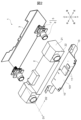
- FIG. FIG. 2 is an exploded perspective view of the imaging device shown in FIG. 1 .
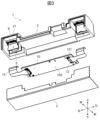
- FIG. 3 is an exploded perspective view of the imaging device as viewed from a different direction than that of FIG. 2 .
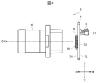
- FIG. 3 is an exploded side view of the camera module shown in FIG. 2 .
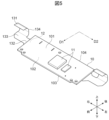
- 3 is a perspective view of a processing board and a flexible wiring member shown in FIG. 2 .
- FIG. 2 is a cross-sectional view of the imaging device taken along line AA shown in FIG. 2 is a diagram illustrating an example of how the imaging device shown in FIG. 1 is installed in a vehicle;
- the imaging direction D1 of the imaging device 1 is also referred to as the "front” of the imaging device 1, and the opposite direction of the imaging direction D1 is also referred to as the "rear” of the imaging device 1.
- the imaging direction D1 is the direction in which the light receiving surface 81 of the imaging element 8 provided in the imaging device 1 faces.
- the upper, lower, left, and right sides when the imaging device 1 is viewed from the “rear” to the “front” are also referred to as the “upper,” “lower,” “left,” and “right” of the imaging device 1, respectively.
- each direction of the imaging device 1 defined in this way coincides with each direction of the vehicle.
- FIG. 1 is a front view of the imaging device 1.
- FIG. 2 is an exploded perspective view of the imaging device 1 shown in FIG. 1.
- FIG. 3 is an exploded perspective view of the imaging device 1 viewed from a different direction than that of FIG. 2.
- FIG. 4 is an exploded side view of the camera module 5 shown in FIG. 2.
- FIG. 5 is a perspective view of the processing board 10 and flexible wiring member 13 shown in FIG. 2.
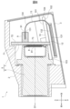
- FIG. 6 is a cross-sectional view of the imaging device 1 taken along line A-A shown in FIG. 1.
- the imaging device 1 is an imaging device such as a monocular camera or a stereo camera that is installed in the vehicle cabin. In this embodiment, the imaging device 1 will be described taking as an example a stereo camera that is installed in the vehicle cabin facing the front of the vehicle.
- the imaging device 1 captures images of subjects such as a road, a preceding vehicle, an oncoming vehicle, a pedestrian, or an obstacle.
- the imaging device 1 simultaneously captures images of the subjects using a pair of camera modules 5.
- the imaging device 1 calculates parallax from the pair of acquired images and measures the distance to the subject or the relative speed, etc.
- the imaging device 1 transmits the measurement results to a control device of the vehicle.
- the control device of the vehicle controls the acceleration, braking, steering, etc. of the vehicle based on the measurement results transmitted from the imaging device 1.
- the imaging device 1 comprises a housing 2, a pair of camera modules 5 that capture images of a subject, a processing board 10 that processes output signals from a pair of imaging boards 7 provided in the pair of camera modules 5, and a pair of flexible wiring members 13 that respectively provide electrical continuity between the pair of imaging boards 7 and the processing board 10.
- the housing 2 houses a pair of camera modules 5, a processing board 10, and a pair of flexible wiring members 13.
- the housing 2 is a metal housing (stay) formed into a long box shape in the left-right direction.
- the housing 2 is manufactured, for example, by aluminum die casting.
- the interior of the housing 2, with the pair of camera modules 5, the processing board 10, and the pair of flexible wiring members 13 housed inside, is covered from below and from the rear by the cover 3.
- the cover 3 is made of a metal plate such as an aluminum plate.
- a pair of camera housing sections 21 that house a pair of camera modules 5 are provided at both left and right ends of the housing 2.
- Each of the pair of camera housing sections 21 is formed in a rectangular box shape.
- a through hole 22 is provided at the front of each of the pair of camera housing sections 21, into which the lens 6 of the camera module 5 is inserted.
- Heat dissipation fins are provided on the top surface of the housing 2 between the pair of camera housing sections 21.
- the camera module 5 includes a lens 6 that forms an image of a subject on the light receiving surface 81 of the imaging element 8, and an imaging board 7, which is a circuit board on which the imaging element 8 is mounted.
- the camera module 5 is fixed to the camera housing portion 21 of the housing 2 with adhesive, screws, or the like.
- the pair of imaging boards 7 included in the pair of camera modules 5 are arranged at a distance from each other along a predetermined direction D2 (left-right direction) perpendicular to the imaging direction D1.
- the imaging board 7 is disposed perpendicular to the imaging direction D1.
- the imaging board 7 has a front surface 71 that faces forward in the imaging direction D1 and has the imaging element 8 mounted thereon, and a rear surface 72 that faces rearward.
- the front surface 71 and rear surface 72 of the imaging board 7 are the principal surfaces that have the largest area among the surfaces that constitute the imaging board 7, and are surfaces that are perpendicular to the imaging direction D1.
- the lens 6 is fixed to the imaging board 7 by an adhesive or the like.
- the imaging element 8 is constituted by an image sensor such as a CMOS (complementary metal oxide semiconductor) or a CCD (charge coupled device).
- a connector 9 to which one end 131 of the flexible wiring member 13 is connected is mounted on the rear surface 72 of the imaging board 7.
- the connector 9 is mounted on the upper part of the rear surface 72 of the imaging board 7.
- the connector 9 is mounted on the rear surface 72 in a position that intersects with the imaging board 7.
- the connector 9 is mounted on the rear surface 72 in a position that is perpendicular to the rear surface 72 of the imaging board 7.
- the connector 9 has an insertion port 91 into which one end 131 of the flexible wiring member 13 is inserted.
- the connector 9 is mounted in a position in which the insertion port 91 opens toward the rear, which is the opposite direction to the imaging direction D1.
- the processing board 10 is disposed between the pair of imaging boards 7 along a predetermined direction D2 (left-right direction) as shown in Figures 2 and 3.
- the processing board 10 is fixed to the housing 2 by adhesive, screws, or the like.
- the processing board 10 is disposed at an angle to the imaging board 7 as shown in Figure 6.
- the processing board 10 is disposed non-parallel to the imaging board 7. That is, the processing board 10 is disposed so that a plane including the processing board 10 intersects (including is perpendicular to) a plane including the imaging board 7.
- the processing substrate 10 has a front end 103 located in front and a rear end 104 located in the rear. As shown in Fig. 6, the processing substrate 10 is disposed below the center 73 of the imaging substrate 7. The processing substrate 10 is disposed at an angle with respect to the imaging direction D1 so that the rear end 104 is located above the front end 103. The processing substrate 10 may be disposed so that the rear end 104 is located at the same height as the front end 103 and is parallel to the imaging direction D1 (i.e. perpendicular to the imaging substrate 7). As shown in Fig. 6, the processing substrate 10 is disposed so that the front end 103 is located forward of the imaging substrate 7 and the rear end 104 is located rearward of the imaging substrate 7.
- the processing board 10 has an upper surface 101 on which multiple circuit elements 11 for processing the output signal of the imaging board 7 are mounted, and a lower surface 102 opposite the upper surface 101.
- the upper surface 101 and the lower surface 102 of the processing board 10 are the principal surfaces with the largest area among the surfaces constituting the processing board 10, and are surfaces disposed at an angle to the imaging board 7.
- the multiple circuit elements 11 are composed of an FPGA (Field Programmable Gate Array), an MPU (Micro Processing Unit), memory, etc.
- Each of the multiple circuit elements 11 is thermally connected to the housing 2 via a heat transfer member such as heat dissipation grease or a heat dissipation sheet.
- a pair of connectors 12 to which the other ends 132 of the pair of flexible wiring members 13 are connected are mounted on the underside 102 of the processing board 10.
- the pair of connectors 12 are mounted on the underside 102 at both left and right ends of the processing board 10.
- the connectors 12 are mounted on the underside 102 in a position that is aligned with the processing board 10.
- the connectors 12 have an insertion port 121 into which the other ends 132 of the flexible wiring members 13 are inserted.
- the connector 12 arranged at the left end of the processing board 10 is mounted with the insertion port 121 opening to the left.
- the connector 12 arranged at the right end of the processing board 10 is mounted with the insertion port 121 opening to the right.
- the flexible wiring member 13 is a flexible wiring member such as an FPC (Flexible Printed Circuits) or FFC.
- the flexible wiring member 13 is curved in a convex shape toward the rear, which is the opposite direction to the imaging direction D1.
- the flexible wiring member 13 protrudes rearward beyond the connector 12 mounted on the processing board 10.
- the flexible wiring member 13 does not protrude rearward beyond the rear end 104 of the processing board 10.
- the flexible wiring member 13 has one end 131 connected to the imaging board 7, the other end 132 connected to the processing board 10, a flat portion 133 extending from the other end 132 along a predetermined direction D2, and a curved portion 134 that is curved in a convex shape toward the rear and extends from the flat portion 133 to the one end 131.
- One end 131 of the flexible wiring member 13 is inserted into the insertion port 91 of the connector 9 mounted on the upper part of the rear surface 72 of the imaging board 7. As a result, one end 131 of the flexible wiring member 13 is connected to the imaging board 7 in a position intersecting the imaging board 7. Specifically, one end 131 of the flexible wiring member 13 is connected to the rear surface 72 of the imaging board 7 in a position perpendicular to the rear surface 72. One end 131 of the flexible wiring member 13 is connected to the upper part of the rear surface 72 of the imaging board 7.
- one end 131 of the flexible wiring member 13 located on the left is connected to the upper part of the rear surface 72 of the imaging board 7 located on the left in a position perpendicular to the rear surface 72 of the imaging board 7 located on the left.
- One end 131 of the flexible wiring member 13 located on the right is connected to the upper part of the rear surface 72 of the imaging board 7 located on the right in a position perpendicular to the rear surface 72 of the imaging board 7 located on the right.
- one end 131 of the flexible wiring member 13 may be connected to the lower or central portion 73 of the rear surface 72 of the imaging board 7 by appropriately changing the mounting position of the connector 9.
- One end 131 of the flexible wiring member 13 may be connected to the rear surface 72 of the imaging board 7 in a position along a cross direction other than the orthogonal direction of the imaging board 7 by appropriately changing the opening direction of the insertion port 91 of the connector 9.
- the other end 132 of the flexible wiring member 13 is inserted into the insertion port 121 of the connector 12 mounted on the underside 102 of the left or right end of the processing board 10.
- the other end 132 of the flexible wiring member 13 is connected to the underside 102 of the processing board 10 in a position aligned with the processing board 10.
- the other end 132 of the flexible wiring member 13 located on the left is connected to the underside 102 of the left end of the processing board 10 in a position aligned with the specified direction D2 (left-right direction).
- the other end 132 of the flexible wiring member 13 located on the right is connected to the underside 102 of the right end of the processing board 10 in a position aligned with the specified direction D2 (left-right direction).
- the flat portion 133 of the flexible wiring member 13 extends from the other end 132 along the predetermined direction D2 (left-right direction). Specifically, the flat portion 133 of the flexible wiring member 13 located on the left extends leftward from the other end 132 of the flexible wiring member 13 to the rear of the connector 9 mounted on the imaging board 7 located on the left. The flat portion 133 of the flexible wiring member 13 located on the right extends rightward from the other end 132 of the flexible wiring member 13 to the rear of the connector 9 mounted on the imaging board 7 located on the right.
- the curved portion 134 of the flexible wiring member 13 protrudes rearward from the flat portion 133, curves rearward in a convex shape, and extends forward to one end 131.
- the curved portion 134 of the flexible wiring member 13 located on the left protrudes rearward from the flat portion 133 of the flexible wiring member 13, curves rearward in a convex shape, and extends forward to one end 131 of the flexible wiring member 13.
- the curved portion 134 of the flexible wiring member 13 located on the right protrudes rearward from the flat portion 133 of the flexible wiring member 13, curves rearward in a convex shape, and extends forward to one end 131 of the flexible wiring member 13.
- the assembly process of the imaging device 1 will be described using Figure 3.
- the assembly process of the imaging device 1 is automated by a robot, but may also be performed manually.
- the camera module 5 and processing board 10 Prior to the assembly process of the imaging device 1, the camera module 5 and processing board 10 are pre-assembled. That is, the imaging element 8 and connector 9 are pre-mounted on the imaging board 7, and the lens 6 is pre-fixed to the imaging board 7.
- the circuit element 11 and connector 12 are pre-mounted on the processing board 10.
- the other end 132 of the flexible wiring member 13 is inserted into the connector 12 of the processing board 10.
- the camera module 5 is fixed to the housing 2.
- the processing board 10 to which the flexible wiring member 13 is connected is fixed to the housing 2 to which the camera module 5 is fixed.
- the flexible wiring member 13 is bent, and one end 131 of the flexible wiring member 13 is inserted into the connector 9 of the imaging board 7.
- the cover 3 is fixed to the housing 2 to which the camera module 5 and processing board 10 are fixed.
- the flexible wiring member 13 is connected to the imaging board 7 before being connected to the processing board 10, there is a possibility that the flexible wiring member 13 will be twisted when being connected to the processing board 10. Therefore, in the assembly process of the imaging device 1, it is preferable to connect the flexible wiring member 13 to the processing board 10 before being connected to the imaging board 7.
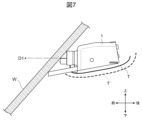
- FIG. 7 is a diagram illustrating an example of vehicle installation of the imaging device 1 shown in FIG. 1.
- the imaging device 1 is installed inside the vehicle cabin facing the front of the vehicle.
- the imaging device 1 is installed near the top of the windshield (front glass) W.
- the installed imaging device 1 is covered with interior material T from below the imaging device 1.
- the FFC protrudes downward from the imaging board, so the interior material T' that covers the installed imaging device needs to be larger than the interior material T of this embodiment, and it tends to protrude downward (towards the seat). Therefore, in order to ensure the driver's forward visibility, conventional imaging devices must be installed as high up as possible, which limits the types of vehicles in which they can be installed.
- the processing board 10 is arranged non-parallel to the imaging board 7, the flexible wiring member 13 is curved in a convex shape toward the rear, which is the opposite direction to the imaging direction D1, and one end 131 of the flexible wiring member 13 is connected to the imaging board 7 in a position in which it crosses the imaging board 7.
- the imaging device 1 forms a space behind the imaging board 7 and can place the flexible wiring member 13 in this space, eliminating the need for the flexible wiring member 13 to protrude below the imaging board 7.
- the imaging device 1 can therefore eliminate the portion that protrudes downward in conventional imaging devices. Therefore, the imaging device 1 can be made smaller without having to reduce the size of the components themselves as the components become more powerful. Therefore, the imaging device 1 can be easily made smaller using existing components.
- the imaging device 1 By making the imaging device 1 smaller, when the imaging device 1 is installed near the top of the windshield W inside the vehicle, the interior material T that covers the imaging device 1 from below can be made smaller than conventional interior material T'.
- the imaging device 1 can make it easier to ensure the driver's forward visibility, and can increase the degree of freedom in the installation position. Therefore, the imaging device 1 can increase the selection of vehicle models in which it can be installed.
- the imaging board 7 has a front surface 71 on which the imaging element 8 is mounted, facing forward in the imaging direction D1, and a rear surface 72 facing backward.
- One end 131 of the flexible wiring member 13 is connected to the rear surface 72 of the imaging board 7.
- the flexible wiring member 13 arranged at the rear of the imaging board 7 must be connected by passing over the outer peripheral end surface of the imaging board 7 and wrapping around the front surface 71 of the imaging board 7. In this case, the flexible wiring member 13 protrudes in the vertical or horizontal directions from the imaging board 7.
- one end 131 of the flexible wiring member 13 is connected to the rear surface 72 of the imaging board 7, so there is no need to wrap the flexible wiring member 13 around the front surface 71 of the imaging board 7. Therefore, the imaging device 1 can be reliably miniaturized because the flexible wiring member 13 does not protrude in the vertical or horizontal directions from the imaging board 7.
- the imaging device 1 can suppress interference between the flexible wiring member 13 and the imaging board 7, so deterioration of the flexible wiring member 13 can be suppressed. Therefore, the imaging device 1 can be easily and reliably miniaturized using existing parts, while making it easier to ensure the reliability of the imaging device 1.
- one end 131 of the flexible wiring member 13 is connected to the rear surface 72 of the imaging board 7 in a position perpendicular to the rear surface 72.
- the imaging device 1 can suppress interference between the electronic components and the flexible wiring member 13. Therefore, the imaging device 1 can be easily miniaturized by using existing components, while allowing greater freedom in component layout.
- the processing board 10 has a front end 103 and a rear end 104.
- the processing board 10 is positioned such that the front end 103 is located forward of the imaging board 7, and the rear end 104 is located rearward of the imaging board 7.
- the imaging device 1 to be smaller in size in the front-to-rear direction. Therefore, the imaging device 1 can be easily made even smaller by using existing parts.
- the imaging board 7 is disposed perpendicular to the imaging direction D1.
- the processing board 10 is disposed below the central portion 73 of the imaging board 7 and is disposed at an angle with respect to the imaging direction D1 so that the rear end portion 104 is positioned above the front end portion 103.
- One end portion 131 of the flexible wiring member 13 is connected to the upper portion of the rear surface 72 of the imaging board 7.
- the imaging device 1 can shorten the length of the flexible wiring member 13 and increase the radius of curvature of the flexible wiring member 13. Therefore, the imaging device 1 can suppress heat generation in the flexible wiring member 13 and reduce stress generated in the flexible wiring member 13, thereby suppressing deterioration of the flexible wiring member 13. Therefore, the imaging device 1 can be easily miniaturized using existing components while making it easier to ensure the reliability of the imaging device 1.
- the processing board 10 has an upper surface 101 on which a circuit element 11 for processing an output signal from the imaging board 7 is mounted, and a lower surface 102 opposite the upper surface 101.
- the other end 132 of the flexible wiring member 13 is connected to the lower surface 102 of the processing board 10 in a position aligned with the processing board 10.
- the imaging device 1 can easily dissipate heat from the circuit elements 11, which generate a large amount of heat, to the housing 2, and also makes it easier to connect the flexible wiring member 13 to the processing board 10 during the assembly process of the imaging device 1. Therefore, the imaging device 1 can be easily miniaturized using existing parts, while making it easier to ensure the reliability and ease of assembly of the imaging device 1.
- the imaging device 1 of this embodiment is a stereo camera installed inside the vehicle cabin facing the front of the vehicle.
- the imaging board 7 is composed of a pair of imaging boards 7 arranged at a distance from each other along a predetermined direction D2 perpendicular to the imaging direction D1.
- the processing board 10 is arranged between the pair of imaging boards 7 along the predetermined direction D2.
- the flexible wiring member 13 is composed of a pair of flexible wiring members 13 that respectively connect the pair of imaging boards 7 and the processing board 10.
- the imaging device 1 is a stereo camera installed inside the vehicle cabin facing the front of the vehicle, it can be easily miniaturized using existing parts.
- the processing board 10 is disposed between the pair of imaging boards 7, the imaging device 1 can be reduced in size in the front-to-rear direction. Therefore, even if the imaging device 1 is a stereo camera installed inside the vehicle cabin facing the front of the vehicle, it can be further easily miniaturized using existing parts.
- the flexible wiring member 13 has one end 131 connected to the imaging board 7, the other end 132 connected to the processing board 10, a flat portion 133 extending from the other end 132 along a predetermined direction D2, and a curved portion 134 curved in a convex shape toward the rear and extending from the flat portion 133 to the one end 131.
- the imaging device 1 does not need to have the flexible wiring member 13 wrap around beyond the rear end 104 of the processing board 10 and around to the top surface 101 of the processing board 10. Therefore, the imaging device 1 can suppress interference between the flexible wiring member 13 and the processing board 10, and can reduce the size in the front-to-rear direction. Therefore, the imaging device 1 can be further easily miniaturized using existing components, while making it easier to ensure the reliability of the imaging device 1.
- the present invention is not limited to the above-described embodiments, but includes various modified examples.
- the above-described embodiments have been described in detail to clearly explain the present invention, and are not necessarily limited to those having all of the configurations described. It is also possible to replace part of the configuration of one embodiment with the configuration of another embodiment, and it is also possible to add the configuration of another embodiment to the configuration of one embodiment. It is also possible to add, delete, or replace part of the configuration of each embodiment with other configurations.
- the above-mentioned configurations, functions, processing units, processing means, etc. may be realized in part or in whole by hardware, for example by designing them as integrated circuits.
- the above-mentioned configurations, functions, etc. may also be realized by software, in which a processor interprets and executes a program that realizes each function.
- Information on the programs, tapes, files, etc. that realize each function can be stored in a memory, a recording device such as a hard disk or SSD (solid state drive), or a recording medium such as an IC card, SD card, or DVD.
- control lines and information lines shown are those considered necessary for the explanation, and do not necessarily show all control lines and information lines on the product. In reality, it can be assumed that almost all components are interconnected.
- 1...imaging device 7...imaging board, 71...front surface, 72...rear surface, 73...center, 8...imaging element, 10...processing board, 101...upper surface, 102...lower surface, 103...front end, 104...rear end, 11...circuit element, 13...flexible wiring member, 131...one end, 132...other end, 133...flat portion, 134...curved portion, D1...imaging direction, D2...predetermined direction
Landscapes
- Engineering & Computer Science (AREA)
- Physics & Mathematics (AREA)
- General Physics & Mathematics (AREA)
- Multimedia (AREA)
- Mechanical Engineering (AREA)
- Signal Processing (AREA)
- Camera Bodies And Camera Details Or Accessories (AREA)
Abstract
Description
上記以外の課題、構成および効果は、以下の実施形態の説明により明らかにされる。
Claims (8)
- 撮像素子が実装された撮像基板と、
前記撮像基板からの出力信号を処理する処理基板と、
前記撮像基板と前記処理基板とを導通させるフレキシブル配線部材と、を備え、
前記処理基板は、前記撮像基板に対して非平行に配置され、
前記フレキシブル配線部材は、撮像方向の反対方向である後方に凸の形状に湾曲し、
前記フレキシブル配線部材の一端部は、前記撮像基板に交差した姿勢で前記撮像基板に接続される
ことを特徴とする撮像装置。 - 前記撮像基板は、前記撮像方向である前方に面し前記撮像素子が実装された前面と、前記後方に面する後面と、を有し、
前記フレキシブル配線部材の前記一端部は、前記撮像基板の前記後面に接続される
ことを特徴とする請求項1に記載の撮像装置。 - 前記フレキシブル配線部材の前記一端部は、前記撮像基板の前記後面に直交した姿勢で当該後面に接続される
ことを特徴とする請求項2に記載の撮像装置。 - 前記処理基板は、前端部と、後端部と、を有し、
前記処理基板は、前記前端部が前記撮像基板よりも前方に位置し、前記後端部が前記撮像基板よりも後方に位置するように配置される
ことを特徴とする請求項2に記載の撮像装置。 - 前記撮像基板は、前記撮像方向に直交して配置され、
前記処理基板は、前端部と、後端部と、を有し、
前記処理基板は、前記撮像基板の中央部よりも下方に配置されると共に、前記後端部が前記前端部よりも上方に位置するよう前記撮像方向に対して傾斜して配置され、
前記フレキシブル配線部材の前記一端部は、前記撮像基板の前記後面の上部に接続される
ことを特徴とする請求項2に記載の撮像装置。 - 前記処理基板は、前記撮像基板の出力信号を処理する回路素子が搭載された上面と、前記上面とは反対側の下面と、を有し、
前記フレキシブル配線部材の他端部は、前記処理基板に沿った姿勢で前記処理基板の前記下面に接続される
ことを特徴とする請求項5に記載の撮像装置。 - 前記撮像装置は、車両前方に向けて車室内に設置されるステレオカメラであり、
前記撮像基板は、前記撮像方向に直交する所定方向に沿って互いに間隔を空けて配置された一対の撮像基板によって構成され、
前記処理基板は、前記所定方向に沿って前記一対の撮像基板の間に配置され、
前記フレキシブル配線部材は、前記一対の撮像基板と前記処理基板とをそれぞれ導通させる一対のフレキシブル配線部材によって構成される
ことを特徴とする請求項2に記載の撮像装置。 - 前記フレキシブル配線部材は、
前記撮像基板に接続される前記一端部と、
前記処理基板に接続される他端部と、
前記他端部から前記所定方向に沿って延びる平坦部と、
前記後方に凸の形状に湾曲し、前記平坦部から前記一端部まで延びる湾曲部と、を有する
ことを特徴とする請求項7に記載の撮像装置。
Priority Applications (2)
| Application Number | Priority Date | Filing Date | Title |
|---|---|---|---|
| PCT/JP2023/012600 WO2024201732A1 (ja) | 2023-03-28 | 2023-03-28 | 撮像装置 |
| JP2025509352A JPWO2024201732A1 (ja) | 2023-03-28 | 2023-03-28 |
Applications Claiming Priority (1)
| Application Number | Priority Date | Filing Date | Title |
|---|---|---|---|
| PCT/JP2023/012600 WO2024201732A1 (ja) | 2023-03-28 | 2023-03-28 | 撮像装置 |
Publications (1)
| Publication Number | Publication Date |
|---|---|
| WO2024201732A1 true WO2024201732A1 (ja) | 2024-10-03 |
Family
ID=92903557
Family Applications (1)
| Application Number | Title | Priority Date | Filing Date |
|---|---|---|---|
| PCT/JP2023/012600 Ceased WO2024201732A1 (ja) | 2023-03-28 | 2023-03-28 | 撮像装置 |
Country Status (2)
| Country | Link |
|---|---|
| JP (1) | JPWO2024201732A1 (ja) |
| WO (1) | WO2024201732A1 (ja) |
Citations (3)
| Publication number | Priority date | Publication date | Assignee | Title |
|---|---|---|---|---|
| DE102010023293A1 (de) * | 2010-06-10 | 2011-12-15 | Hella Kgaa Hueck & Co. | Kamera für ein Kraftfahrzeug |
| JP2016046754A (ja) * | 2014-08-26 | 2016-04-04 | 日立オートモティブシステムズ株式会社 | 車載用カメラ |
| JP2019089528A (ja) * | 2017-11-10 | 2019-06-13 | 株式会社デンソー | カメラモジュール |
-
2023
- 2023-03-28 JP JP2025509352A patent/JPWO2024201732A1/ja active Pending
- 2023-03-28 WO PCT/JP2023/012600 patent/WO2024201732A1/ja not_active Ceased
Patent Citations (3)
| Publication number | Priority date | Publication date | Assignee | Title |
|---|---|---|---|---|
| DE102010023293A1 (de) * | 2010-06-10 | 2011-12-15 | Hella Kgaa Hueck & Co. | Kamera für ein Kraftfahrzeug |
| JP2016046754A (ja) * | 2014-08-26 | 2016-04-04 | 日立オートモティブシステムズ株式会社 | 車載用カメラ |
| JP2019089528A (ja) * | 2017-11-10 | 2019-06-13 | 株式会社デンソー | カメラモジュール |
Also Published As
| Publication number | Publication date |
|---|---|
| JPWO2024201732A1 (ja) | 2024-10-03 |
Similar Documents
| Publication | Publication Date | Title |
|---|---|---|
| US12208750B2 (en) | Vehicular camera with pliable material disposed between and contacting stacked PCBs | |
| JP7262626B2 (ja) | 撮像装置 | |
| EP3512316B1 (en) | Electronic device, camera apparatus, and shield chassis | |
| JP7328398B2 (ja) | 電子機器、撮像装置、および移動体 | |
| US12069226B2 (en) | Imaging device | |
| US20150358605A1 (en) | Stereo camera module and method for the production thereof | |
| JP7234044B2 (ja) | ステレオカメラ | |
| US20180147999A1 (en) | Video-camera device for a motor vehicle and assembly method | |
| JP6533572B2 (ja) | 撮像装置 | |
| WO2021117462A1 (ja) | 撮像装置 | |
| JP2016046754A (ja) | 車載用カメラ | |
| US11997373B2 (en) | Camera module for a vehicle | |
| CN113632446B (zh) | 电子设备、拍摄装置以及移动体 | |
| WO2023276232A1 (ja) | 撮像装置 | |
| JP7224514B2 (ja) | 電子機器、撮像装置、および移動体 | |
| WO2025120811A1 (ja) | 撮像装置 | |
| JP7548786B2 (ja) | カメラ装置 | |
| JP7646102B2 (ja) | カメラユニット | |
| JP2025109630A (ja) | 撮像装置 | |
| WO2020121746A1 (ja) | ステレオカメラ装置 | |
| CN112334735A (zh) | 立体摄像装置 |
Legal Events
| Date | Code | Title | Description |
|---|---|---|---|
| 121 | Ep: the epo has been informed by wipo that ep was designated in this application |
Ref document number: 23930372 Country of ref document: EP Kind code of ref document: A1 |
|
| ENP | Entry into the national phase |
Ref document number: 2025509352 Country of ref document: JP Kind code of ref document: A |
|
| WWE | Wipo information: entry into national phase |
Ref document number: 2025509352 Country of ref document: JP |
|
| NENP | Non-entry into the national phase |
Ref country code: DE |
|
| 122 | Ep: pct application non-entry in european phase |
Ref document number: 23930372 Country of ref document: EP Kind code of ref document: A1 |