WO2024195643A1 - 半導体発光装置 - Google Patents
半導体発光装置 Download PDFInfo
- Publication number
- WO2024195643A1 WO2024195643A1 PCT/JP2024/009702 JP2024009702W WO2024195643A1 WO 2024195643 A1 WO2024195643 A1 WO 2024195643A1 JP 2024009702 W JP2024009702 W JP 2024009702W WO 2024195643 A1 WO2024195643 A1 WO 2024195643A1
- Authority
- WO
- WIPO (PCT)
- Prior art keywords
- wires
- electrode
- light emitting
- substrate
- wire
- Prior art date
- Legal status (The legal status is an assumption and is not a legal conclusion. Google has not performed a legal analysis and makes no representation as to the accuracy of the status listed.)
- Ceased
Links
Images


Classifications
-
- H—ELECTRICITY
- H01—ELECTRIC ELEMENTS
- H01S—DEVICES USING THE PROCESS OF LIGHT AMPLIFICATION BY STIMULATED EMISSION OF RADIATION [LASER] TO AMPLIFY OR GENERATE LIGHT; DEVICES USING STIMULATED EMISSION OF ELECTROMAGNETIC RADIATION IN WAVE RANGES OTHER THAN OPTICAL
- H01S5/00—Semiconductor lasers
- H01S5/02—Structural details or components not essential to laser action
- H01S5/022—Mountings; Housings
- H01S5/0233—Mounting configuration of laser chips
- H01S5/02345—Wire-bonding
-
- H—ELECTRICITY
- H01—ELECTRIC ELEMENTS
- H01S—DEVICES USING THE PROCESS OF LIGHT AMPLIFICATION BY STIMULATED EMISSION OF RADIATION [LASER] TO AMPLIFY OR GENERATE LIGHT; DEVICES USING STIMULATED EMISSION OF ELECTROMAGNETIC RADIATION IN WAVE RANGES OTHER THAN OPTICAL
- H01S5/00—Semiconductor lasers
- H01S5/04—Processes or apparatus for excitation, e.g. pumping, e.g. by electron beams
- H01S5/042—Electrical excitation ; Circuits therefor
- H01S5/0425—Electrodes, e.g. characterised by the structure
- H01S5/04256—Electrodes, e.g. characterised by the structure characterised by the configuration
-
- H—ELECTRICITY
- H01—ELECTRIC ELEMENTS
- H01S—DEVICES USING THE PROCESS OF LIGHT AMPLIFICATION BY STIMULATED EMISSION OF RADIATION [LASER] TO AMPLIFY OR GENERATE LIGHT; DEVICES USING STIMULATED EMISSION OF ELECTROMAGNETIC RADIATION IN WAVE RANGES OTHER THAN OPTICAL
- H01S5/00—Semiconductor lasers
- H01S5/40—Arrangement of two or more semiconductor lasers, not provided for in groups H01S5/02 - H01S5/30
- H01S5/4025—Array arrangements, e.g. constituted by discrete laser diodes or laser bar
- H01S5/4031—Edge-emitting structures
-
- H—ELECTRICITY
- H10—SEMICONDUCTOR DEVICES; ELECTRIC SOLID-STATE DEVICES NOT OTHERWISE PROVIDED FOR
- H10W—GENERIC PACKAGES, INTERCONNECTIONS, CONNECTORS OR OTHER CONSTRUCTIONAL DETAILS OF DEVICES COVERED BY CLASS H10
- H10W72/00—Interconnections or connectors in packages
- H10W72/071—Connecting or disconnecting
Definitions
- This disclosure relates to a semiconductor light-emitting device.
- a configuration is known in which an edge-emitting semiconductor laser is used as the light source for a semiconductor light-emitting device (see, for example, Patent Document 1).
- a configuration including multiple light-emitting sections is known for the purpose of increasing the output of edge-emitting elements such as edge-emitting semiconductor lasers.
- edge-emitting elements such as edge-emitting semiconductor lasers.
- the semiconductor light emitting device that solves the above problem includes a substrate having a substrate front surface and a substrate back surface, an end surface light emitting element disposed on the substrate and having a plurality of light emitting units arranged in a first direction intersecting the thickness direction of the substrate in a plan view, a plurality of surface electrodes formed on the substrate surface and disposed at a distance from each other, and a plurality of wires electrically connecting the plurality of light emitting units and the plurality of surface electrodes, the plurality of light emitting units including a first light emitting unit provided with a first element electrode and a second light emitting unit provided with a second element electrode, the plurality of surface electrodes including a first surface electrode electrically connected to the first element electrode and a second surface electrode electrically connected to the second element electrode, the plurality of wires including a plurality of first wires electrically connecting the first element electrode and the first surface electrode, and a plurality of second wires electrically connecting the second element electrode and the second surface electrode, and in a
- the above semiconductor light-emitting device can reduce the variation in the pulse width of light emitted when a voltage is applied to the end-face light-emitting element.
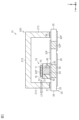
- FIG. 1 is a perspective view of a semiconductor light emitting device according to the first embodiment.
- FIG. 2 is a plan view that illustrates a schematic internal structure of the semiconductor light emitting device of FIG.
- FIG. 3 is a rear view of the semiconductor light emitting device of FIG.
- FIG. 4 is a cross-sectional view that illustrates a schematic cross-sectional structure of the semiconductor light-emitting device taken along line F4-F4 in FIG.
- FIG. 5 is a cross-sectional view that illustrates a schematic cross-sectional structure of the semiconductor light-emitting device taken along line F5-F5 in FIG.
- FIG. 6 is a schematic cross-sectional view of the semiconductor light emitting device of FIG. FIG.
- FIG. 7 is an enlarged view of a part of the surface electrode and its periphery in a state where the wires are omitted from the semiconductor light emitting device of FIG.
- FIG. 8 is an enlarged view of a part of the front electrode and its periphery in the semiconductor light emitting device of FIG.
- FIG. 9 is a plan view that illustrates a schematic internal structure of a semiconductor light emitting device of a comparative example.
- FIG. 10 is a plan view illustrating a schematic internal structure of the semiconductor light emitting device according to the second embodiment.
- FIG. 11 is a plan view illustrating a schematic internal structure of a semiconductor light emitting device according to the third embodiment.
- FIG. 12 is an enlarged view of a part of the front electrode and its periphery in the semiconductor light emitting device of FIG.
- FIG. 13 is an enlarged plan view of a part of the front electrode and its periphery in a semiconductor light emitting device according to a modified example.
- FIG. 14 is an enlarged plan view of a part of the front surface electrode and its periphery in a semiconductor light emitting device according to a modified example.
- FIG. 15 is an enlarged plan view of a part of the front surface electrode and its periphery in a semiconductor light emitting device according to a modified example.
- FIG. 16 is a plan view illustrating a schematic internal structure of a semiconductor light emitting device according to a modified example.
- FIG. 17 is a plan view illustrating a schematic internal structure of a semiconductor light emitting device according to a modified example.
- FIG. 18 is a plan view illustrating a schematic internal structure of a semiconductor light emitting device according to a modified example.
- FIG. 19 is a plan view illustrating a schematic internal structure of a semiconductor light emitting device according to a modified example.
- Figure 1 shows a perspective structure of the semiconductor light emitting device 10.
- Figure 2 shows a schematic planar structure of the inside of the semiconductor light emitting device 10.
- Figure 3 shows a schematic back structure of the semiconductor light emitting device 10.
- Figure 4 is a cross-sectional view of the semiconductor light emitting device 10 taken along line F4-F4 in Figure 2
- Figure 5 is a cross-sectional view of the semiconductor light emitting device 10 taken along line F5-F5 in Figure 2.
- Figure 6 shows a cross-sectional structure of the semiconductor light emitting device 10 as viewed from the light emitting surface.
- a wire 100 which will be described later, is omitted in order to facilitate understanding of the drawings.
- the semiconductor light emitting device 10 includes a rectangular flat substrate 20, an end surface light emitting element 70 (see FIG. 2) provided on the substrate 20, and a case 200 provided on the substrate 20 to house the end surface light emitting element 70.
- the thickness direction of the substrate 20 is referred to as the "Z direction”.
- Two mutually orthogonal directions among the directions perpendicular to the Z direction are referred to as the "X direction” and the "Y direction”.
- “planar view” refers to the semiconductor light emitting device 10 being viewed from the thickness direction (Z direction) of the substrate 20.
- the substrate 20 is formed in a rectangular shape with the X direction being the longitudinal direction and the Y direction being the lateral direction in a planar view.
- the substrate 20 has a substrate front surface 21 and a substrate back surface 22 that face opposite each other in the Z direction, and first to fourth substrate side surfaces 23 to 26 that intersect with the substrate front surface 21 and the substrate back surface 22.
- both the substrate front surface 21 and the substrate back surface 22 are formed as planes perpendicular to the Z direction.
- the first to fourth substrate side surfaces 23 to 26 are planes perpendicular to the substrate front surface 21 and the substrate back surface 22.
- the first substrate side surface 23 and the second substrate side surface 24 form both end surfaces of the substrate 20 in the X direction
- the third substrate side surface 25 and the fourth substrate side surface 26 form both end surfaces of the substrate 20 in the Y direction.
- the substrate 20 is formed of, for example, glass epoxy resin.
- the substrate 20 may be formed of a material containing ceramic.
- the material containing ceramic include aluminum nitride (AlN) and alumina (Al 2 O 3 ).
- AlN aluminum nitride
- Al 2 O 3 alumina
- the edge-emitting element 70 is, for example, a laser diode that emits light in a predetermined wavelength band, and functions as a light source for the semiconductor light-emitting device 10.
- the edge-emitting element 70 is an edge-emitting laser element.
- a Fabry-Perot type laser diode element is used.
- the edge-emitting element 70 is configured to emit light toward the fourth substrate side surface 26 in a plan view.
- the case 200 is formed in a box shape that opens in the Z direction toward the substrate 20.
- the case 200 has first to fourth side walls 211 to 214 that are formed in a rectangular frame shape in a plan view, and a top wall 215 that covers one end in the Z direction of the opening formed by the first to fourth side walls 211 to 214.
- the first to fourth side walls 211 to 214 and the top wall 215 are formed integrally.
- the first side wall 211 and the second side wall 212 form the side walls at both ends of the case 200 in the X direction
- the third side wall 213 and the fourth side wall 214 form the side walls at both ends of the case 200 in the Y direction.
- the first side wall 211 forms the side wall closer to the first substrate side surface 23 of the substrate 20, and the second side wall 212 forms the side wall closer to the second substrate side surface 24 of the substrate 20, of the side walls at both ends of the X direction of the case 200.
- the third side wall 213 constitutes the side wall closer to the third substrate side surface 25 of the substrate 20 of the side walls at both ends in the Y direction of the case 200, and the fourth side wall 214 constitutes the side wall closer to the fourth substrate side surface 26 of the substrate 20.
- the first to third side walls 211 to 213 and the top wall 215 are formed semi-transparently, and the fourth side wall 214 is formed transparently.
- the fourth side wall 214 is a side surface disposed in the emission direction of the end surface light emitting element 70. Note that the case 200 only needs to be transparent at least in the emission direction of the end surface light emitting element 70. Therefore, at least one of the first to third side walls 211 to 213 and the top wall 215 may be formed transparently like the fourth side wall 214.
- the case 200 is formed, for example, from a glass material. Note that instead of a glass material, the case 200 may be formed from a transparent or translucent resin material. Examples of such resin materials include acrylic resin and epoxy resin.
- the semiconductor light emitting device 10 has a plurality of surface electrodes 30 (ten in the first embodiment) formed on the substrate surface 21 of the substrate 20.
- the surface electrodes 30 are arranged spaced apart from one another.
- the surface electrodes 30 are formed of, for example, copper foil. Note that the material of the surface electrodes 30 is not limited to copper (Cu), and may include at least one of aluminum (Al), nickel (Ni), palladium (Pd), silver (Ag), and gold (Au).
- the multiple surface electrodes 30 include first inner surface electrodes 31P, 31Q, second inner surface electrodes 32P, 32Q, outer surface electrodes 33P, 33Q, and end surface electrodes 34P, 34Q.
- the first inner surface electrodes 31P, 31Q, second inner surface electrodes 32P, 32Q, outer surface electrodes 33P, 33Q, and end surface electrodes 34P, 34Q are surface electrodes electrically connected to the end light emitting element 70.
- the first inner surface electrode 31P, the second inner surface electrode 32P, the outer surface electrode 33P, and the end surface electrode 34P are each formed in an area of the substrate surface 21 closer to the first substrate side surface 23 than a center virtual line CL (two-dot chain line) that extends along the Y direction at the center of the X direction of the substrate 20.
- the first inner surface electrode 31Q, the second inner surface electrode 32Q, the outer surface electrode 33Q, and the end surface electrode 34Q are each formed in an area of the substrate surface 21 closer to the second substrate side surface 24 than the center virtual line CL.
- the first inner surface electrode 31P, the second inner surface electrode 32P, the outer surface electrode 33P, and the end surface electrode 34P are symmetrical with respect to the center virtual line CL in a plan view.
- the first inner surface electrode 31P, the second inner surface electrode 32P, and the outer surface electrode 33P are arranged spaced apart from one another in the X direction while being aligned with one another in the Y direction.
- the first inner surface electrode 31P is disposed closer to the central virtual line CL (the center of the substrate surface 21 in the X direction) than the second inner surface electrode 32P and the outer surface electrode 33P.
- the outer surface electrode 33P is disposed closer to the first substrate side surface 23 than the first inner surface electrode 31P and the second inner surface electrode 32P. For this reason, it can be said that the outer surface electrode 33P is disposed closer to the edge of the substrate surface 21 than the first inner surface electrode 31P and the second inner surface electrode 32P.
- the end surface electrode 34P is disposed closer to the first substrate side surface 23 than the end surface light emitting element 70.
- the end surface electrode 34P is disposed offset closer to the fourth substrate side surface 26 than the first inner surface electrode 31P, the second inner surface electrode 32P, and the outer surface electrode 33P.
- the end surface electrode 34P includes a portion that overlaps with the outer surface electrode 33P and a portion that protrudes closer to the fourth substrate side surface 26 than the outer surface electrode 33P.
- the first inner surface electrode 31Q, the second inner surface electrode 32Q, and the outer surface electrode 33Q are arranged spaced apart from one another in the X direction while being aligned with one another in the Y direction.
- the first inner surface electrode 31Q is arranged closer to the center virtual line CL (the center of the substrate surface 21 in the X direction) than the second inner surface electrode 32Q and the outer surface electrode 33Q.
- the outer surface electrode 33Q is arranged closer to the second substrate side surface 24 than the first inner surface electrode 31Q and the second inner surface electrode 32Q.
- the first inner surface electrodes 31P, 31Q are arranged adjacent to one another across the center virtual line CL.
- the end surface electrode 34Q is disposed closer to the second substrate side surface 24 than the end surface light emitting element 70.
- the end surface electrode 34Q is disposed shifted closer to the fourth substrate side surface 26 than the first inner surface electrode 31Q, the second inner surface electrode 32Q, and the outer surface electrode 33Q.
- the end surface electrode 34Q includes a portion that overlaps with the outer surface electrode 33Q and a portion that protrudes closer to the fourth substrate side surface 26 than the outer surface electrode 33Q.
- the sides closer to the central virtual line CL are considered to be "inside”
- the sides closer to the first substrate side surface 23 and the second substrate side surface 24 are considered to be "outside”.
- first inner surface electrodes 31P, 31Q The detailed shapes of the first inner surface electrodes 31P, 31Q, the second inner surface electrodes 32P, 32Q, the outer surface electrodes 33P, 33Q, and the end surface electrodes 34P, 34Q will be described later.
- the multiple surface electrodes 30 include a mounting pattern 35 and an adhesive pattern 36 formed on the substrate surface 21 of the substrate 20 .
- the mounting pattern 35 is disposed on the substrate surface 21 closer to the fourth substrate side surface 26 than the first inner surface electrodes 31P, 31Q, the second inner surface electrodes 32P, 32Q, and the outer surface electrodes 33P, 33Q.
- the mounting pattern 35 is disposed on the substrate surface 21 between the end surface electrodes 34P, 34Q in the X direction.
- the mounting pattern 35 is formed in a rectangular shape with the X direction being the longitudinal direction and the Y direction being the lateral direction. When viewed from the Y direction, the mounting pattern 35 extends in the X direction so as to overlap with the first inner surface electrodes 31P, 31Q, the second inner surface electrodes 32P, 32Q, and the outer surface electrodes 33P, 33Q.
- the adhesive pattern 36 is formed in a frame shape surrounding the first inner surface electrodes 31P, 31Q, the second inner surface electrodes 32P, 32Q, the outer surface electrodes 33P, 33Q, the end surface electrodes 34P, 34Q, and the mounting pattern 35.
- the adhesive pattern 36 is formed in a rectangular frame shape with the X direction being the longitudinal direction and the Y direction being the lateral direction.
- the adhesive pattern 36 is a pattern on which adhesive is applied to adhere the case 200, and is not electrically connected to the end light emitting element 70. For this reason, the adhesive pattern 36 is in an electrically floating state.
- the adhesive pattern 36 may be formed of a material different from that of the other surface electrodes 30. In one example, the adhesive pattern 36 may be formed of an insulating material.
- the surface electrode 30 does not include the adhesive pattern 36.
- the semiconductor light emitting device 10 includes a plurality of surface electrodes 30 and the adhesive pattern 36.
- the adhesive pattern 36 surrounds the plurality of surface electrodes 30 in a plan view.
- a surface resist 37 is provided on the substrate surface 21.
- the surface resist 37 is formed in a U-shape surrounding the mounting pattern 35 from both sides in the X direction and from the third substrate side surface 25 side in the Y direction.
- the surface resist 37 is formed between the mounting pattern 35 and the first inner surface electrodes 31P, 31Q, the second inner surface electrodes 32P, 32Q, the outer surface electrodes 33P, 33Q, and the end surface electrodes 34P, 34Q.
- the surface resist 37 is provided so as to contact the side of the mounting pattern 35.
- the surface resist 37 is separated from the first inner surface electrodes 31P, 31Q, the second inner surface electrodes 32P, 32Q, the outer surface electrodes 33P, 33Q, and the end surface electrodes 34P, 34Q.
- the surface resist 37 is a solder resist, and is formed of, for example, an insulating material.
- an epoxy resin can be used as the insulating material.
- the semiconductor light emitting device 10 includes a submount substrate 90 that supports the end surface light emitting element 70.
- the submount substrate 90 is mounted on the mounting pattern 35.
- the submount substrate 90 is die bonded to the mounting pattern 35. Note that the mounting pattern 35 may be integrated with the submount substrate 90.
- the die bonding material (not shown) used to die bond the submount substrate 90 to the mounting pattern 35 tends to remain on the mounting pattern 35 due to the surface resist 37. This makes it possible to prevent the mounting pattern 35 from being electrically connected to the first inner surface electrodes 31P, 31Q, the second inner surface electrodes 32P, 32Q, the outer surface electrodes 33P, 33Q, and the end surface electrodes 34P, 34Q by the conductive bonding material.
- die bonding materials include solder paste, silver paste, gold paste, and copper paste.
- the submount substrate 90 is formed in a rectangular flat plate shape.
- the submount substrate 90 is formed in a rectangular shape with the X direction being the longitudinal direction and the Y direction being the lateral direction in a plan view.
- the submount substrate 90 is slightly smaller than the mounting pattern 35 in a plan view.
- the submount substrate 90 is formed of a material containing silicon (Si), for example.
- the submount substrate 90 may be formed of a material containing ceramic. Examples of the material containing ceramic include AlN and Al 2 O 3.
- the submount substrate 90 may be formed of a material containing Cu.
- the thickness of the submount substrate 90 is greater than the thickness of the substrate 20. Note that the thickness of the submount substrate 90 can be changed as desired, and may be, for example, less than or equal to the thickness of the substrate 20.
- the submount substrate 90 has a front surface 91 and a back surface 92 that face opposite each other in the Z direction.
- both the front surface 91 and the back surface 92 are formed as planes perpendicular to the Z direction.
- the front surface 91 faces the same side as the substrate front surface 21, and the back surface 92 faces the same side as the substrate back surface 22.
- An end surface light emitting element 70 is mounted on the front surface 91 of the submount substrate 90. In one example, the end surface light emitting element 70 is die bonded to the front surface 91 of the submount substrate 90.
- the submount substrate 90 is provided with through-wires 93 penetrating in the thickness direction.
- the through-wires 93 are formed of a material containing Cu, for example.
- the material of the through-wires 93 is not limited to Cu, and may contain at least one of titanium (Ti), tungsten (W), and Al.
- the number of through-wires 93 can be changed arbitrarily. In one example, a plurality of through-wires 93 may be provided. In one example, the number of through-wires 93 may be the same as the number of element electrodes 80 (eight in this embodiment) of the end-surface light-emitting element 70, which will be described later.
- the submount substrate 90 is formed of a material containing Cu, the entire submount substrate 90 is made of a conductor, so the through-wires 93 can be omitted.
- the end surface light emitting element 70 provided on the submount substrate 90 is formed in a rectangular flat plate shape.
- the end surface light emitting element 70 has a rectangular shape with the X direction as the long side and the Y direction as the short side.
- the end surface light emitting element 70 is slightly smaller than the submount substrate 90.
- the end surface light emitting element 70 is disposed in the center of the substrate 20 in the X direction. For this reason, it can be said that the central virtual line CL is located in the center of the end surface light emitting element 70 in the X direction.
- the thickness of the end surface light emitting element 70 is thinner than the thickness of the submount substrate 90.
- the thickness of the end surface light emitting element 70 is also thinner than the thickness of the substrate 20.
- the thickness of the end surface light emitting element 70 can be changed as desired, and may be, for example, greater than or equal to the thickness of the substrate 20.
- the end surface light emitting element 70 has an element front surface 71 and an element back surface 72 facing opposite each other in the Z direction, and first to fourth element side surfaces 73 to 76 intersecting with the element front surface 71 and the element back surface 72.
- both the element front surface 71 and the element back surface 72 are formed as planes perpendicular to the Z direction.
- the first to fourth element side surfaces 73 to 76 are planes perpendicular to the element front surface 71 and the element back surface 72.
- the first element side surface 73 and the second element side surface 74 constitute both end surfaces of the end surface light emitting element 70 in the X direction
- the third element side surface 75 and the fourth element side surface 76 constitute both end surfaces of the end surface light emitting element 70 in the Y direction.
- the first element side surface 73 constitutes the end surface closer to the first substrate side surface 23 of the end surface light emitting element 70 in the X direction
- the second element side surface 74 constitutes the end surface closer to the second substrate side surface 24 of the end surface light emitting element 70 in the X direction.
- the third element side surface 75 constitutes the end surface closer to the third substrate side surface 25 of both end surfaces of the end surface light emitting element 70 in the Y direction
- the fourth element side surface 76 constitutes the end surface closer to the fourth substrate side surface 26 of both end surfaces of the end surface light emitting element 70 in the Y direction.
- the fourth element side surface 76 constitutes the light emitting end surface that emits light from the end surface light emitting element 70.
- the end surface light emitting element 70 has a plurality of element electrodes 80 (eight in the first embodiment) formed on the element surface 71.
- the end surface light emitting element 70 has a light emitting portion 80A (80B) for each of the plurality of element electrodes 80.
- the end surface light emitting element 70 has a plurality of light emitting portions 80A (80B) (eight in the first embodiment).
- the plurality of light emitting portions 80A (80B) are arranged in the X direction.
- the four light emitting portions closer to the first substrate side surface 23 than the central virtual line CL are referred to as "light emitting portions 80A”
- the four light emitting portions closer to the second substrate side surface 24 than the central virtual line CL are referred to as "light emitting portions 80B”.
- the X direction corresponds to the "first direction”.
- the Y direction corresponds to the "second direction”.
- the multiple light-emitting sections 80A include first inner light-emitting sections 81A, 81B, second inner light-emitting sections 82A, 82B, outer light-emitting sections 83A, 83B, and end light-emitting sections 84A, 84B.
- the first inner light-emitting portion 81A is a light-emitting portion provided with a first inner element electrode 81P, which will be described later, and the first inner light-emitting portion 81B is a light-emitting portion provided with a first inner element electrode 81Q.
- the first inner light-emitting portion 81A is a light-emitting portion that emits light when a voltage is applied to the first inner element electrode 81P
- the first inner light-emitting portion 81B is a light-emitting portion that emits light when a voltage is applied to the first inner element electrode 81Q.
- the second inner light-emitting portion 82A is a light-emitting portion provided with a second inner element electrode 82P, which will be described later, and the second inner light-emitting portion 82B is a light-emitting portion provided with a second inner element electrode 82Q.
- the second inner light-emitting portion 82A is a light-emitting portion that emits light when a voltage is applied to the second inner element electrode 82P
- the second inner light-emitting portion 82B is a light-emitting portion that emits light when a voltage is applied to the second inner element electrode 82Q.
- the outer light-emitting portion 83A is a light-emitting portion provided with an outer element electrode 83P, which will be described later, and the outer light-emitting portion 83B is a light-emitting portion provided with an outer element electrode 83Q.
- the outer light-emitting portion 83A is a light-emitting portion that emits light when a voltage is applied to the outer element electrode 83P
- the outer light-emitting portion 83B is a light-emitting portion that emits light when a voltage is applied to the outer element electrode 83Q.
- the end light-emitting portion 84A is a light-emitting portion provided with an end element electrode 84P, which will be described later, and the end light-emitting portion 84B is a light-emitting portion provided with an end element electrode 84Q.
- the end light-emitting portion 84A is a light-emitting portion that emits light when a voltage is applied to the end element electrode 84P
- the end light-emitting portion 84B is a light-emitting portion that emits light when a voltage is applied to the end element electrode 84Q.
- the first inner element electrode 81P (81Q) corresponds to the "first element electrode", and the first inner light-emitting portion 81A (81B) corresponds to the "first light-emitting portion”.
- the second inner element electrode 82P (82Q) may correspond to the "first element electrode”, and the second inner light-emitting portion 82A (82B) may correspond to the "first light-emitting portion”.
- the outer element electrode 83P (83Q) may correspond to the "second element electrode", and the outer light-emitting portion 83A (83B) may correspond to the "second light-emitting portion”.
- the multiple element electrodes 80 are arranged at intervals in the X direction in a plan view. Therefore, it can be said that the multiple light emitting sections 80A (80B) are arranged at intervals in the X direction in a plan view.
- Each element electrode 80 is formed in a rectangular shape with the Y direction as the long side and the X direction as the short side in a plan view.
- the multiple element electrodes 80 are formed, for example, from Au. Note that the constituent material of the multiple element electrodes 80 is not limited to Au, and may include at least one of Al, Ni, Pd, Ag, and Cu.
- the multiple element electrodes 80 include first inner element electrodes 81P, 81Q, second inner element electrodes 82P, 82Q, outer element electrodes 83P, 83Q, and end element electrodes 84P, 84Q.
- Each of the first inner element electrode 81P, the second inner element electrode 82P, the outer element electrode 83P, and the end element electrode 84P is formed in a region of the element surface 71 closer to the first element side surface 73 than the central virtual line CL.
- Each of the first inner element electrode 81Q, the second inner element electrode 82Q, the outer element electrode 83Q, and the end element electrode 84Q is formed in a region of the element surface 71 closer to the second element side surface 74 than the central virtual line CL.
- the first inner element electrode 81P is disposed closer to the central imaginary line CL (the center in the X direction of the end surface light emitting element 70) than the second inner element electrode 82P, the outer element electrode 83P, and the end element electrode 84P.
- the end element electrode 84P is disposed closer to the first element side surface 73 than the first inner element electrode 81P, the second inner element electrode 82P, and the outer element electrode 83P. It can be said that the end element electrode 84P is disposed at the end of the element surface 71 that is closer to the first element side surface 73 in the X direction.
- the outer element electrode 83P is disposed closer to the end element electrode 84P than the first inner element electrode 81P and the second inner element electrode 82P.
- the first inner element electrode 81Q is arranged closer to the center virtual line CL (the center in the X-direction of the end surface light emitting element 70) than the second inner element electrode 82Q, the outer element electrode 83Q, and the end element electrode 84Q.
- the end element electrode 84Q is arranged closer to the second element side surface 74 than the first inner element electrode 81Q, the second inner element electrode 82Q, and the outer element electrode 83Q. It can be said that the end element electrode 84Q is arranged at the end closer to the second element side surface 74 of both ends in the X-direction of the element surface 71.
- the outer element electrode 83Q is arranged closer to the end element electrode 84Q than the first inner element electrode 81Q and the second inner element electrode 82Q.
- the side closer to the central virtual line CL (the center of the end surface light emitting element 70 in the X direction) is defined as the "inside”
- the side closer to the first element side surface 73 and the second element side surface 74 is defined as the "outside”.
- the end surface light emitting element 70 includes a back electrode 85.
- the back electrode 85 constitutes the element back surface 72 of the end surface light emitting element 70.
- the back electrode 85 is formed over the entire element back surface 72 of the end surface light emitting element 70.
- the back electrode 85 is formed of, for example, Au. Note that the constituent material of the back electrode 85 is not limited to Au, and may include at least one of Al, Ni, Pd, Ag, and Cu.
- the end surface light emitting element 70 is mounted on the submount substrate 90 by a conductive bonding material (not shown). Therefore, the back electrode 85 is electrically connected to the submount substrate 90 (through wiring 93) by the conductive bonding material.
- conductive bonding materials include solder paste, silver paste, gold paste, and copper paste.
- the semiconductor light-emitting device 10 includes a plurality of wires 100 that electrically connect the plurality of light-emitting portions 80A (80B) and the plurality of surface electrodes 30 individually.
- the plurality of wires 100 are, for example, bonding wires.
- the plurality of wires 100 are formed of a material that contains, for example, Au.
- the plurality of wires 100 may be formed of a material that contains at least one of Cu, Ag, and Al instead of Au.
- the multiple wires 100 include multiple first inner wires 110P, 110Q, multiple second inner wires 120P, 120Q, multiple outer wires 130P, 130Q, and multiple end wires 140P, 140Q.
- first inner wire 110P corresponds to the "first wire.”
- second inner wire 120P may correspond to the "first wire.”
- the outer wire 130P corresponds to the "second wire.”
- the number of the multiple wires 100 is set according to the diameter of the wires 100 and the size of the element electrode 80 in a planar view.
- the number of the first inner wires 110P, the number of the first inner wires 110Q, the number of the second inner wires 120P, the number of the second inner wires 120Q, the number of the outer wires 130P, the number of the outer wires 130Q, the number of the end wires 140P, and the number of the end wires 140Q are equal to one another.
- the first inner wire 110P, the first inner wire 110Q, the second inner wire 120P, the second inner wire 120Q, the outer wire 130P, the outer wire 130Q, the end wire 140P, and the end wire 140Q each have a maximum of four wires.
- first inner wire 110P, the first inner wire 110Q, the second inner wire 120P, the second inner wire 120Q, the outer wire 130P, the outer wire 130Q, the end wire 140P, and the end wire 140Q each may have, for example, three or five wires.
- Each of the multiple first inner wires 110P is bonded to both the first inner element electrode 81P and the first inner surface electrode 31P of the end surface light emitting element 70.
- the first inner element electrode 81P and the first inner surface electrode 31P are electrically connected by the multiple first inner wires 110P.
- Each of the multiple first inner wires 110Q is bonded to both the first inner element electrode 81Q and the first inner surface electrode 31Q.
- the first inner element electrode 81Q and the first inner surface electrode 31Q are electrically connected by the multiple first inner wires 110Q.
- Each of the multiple second inner wires 120P is bonded to both the second inner element electrode 82P and the second inner surface electrode 32P of the end surface light emitting element 70.
- the second inner element electrode 82P and the second inner surface electrode 32P are electrically connected by the multiple second inner wires 120P.
- Each of the multiple second inner wires 120Q is bonded to both the second inner element electrode 82Q and the second inner surface electrode 32Q.
- the second inner element electrode 82Q and the second inner surface electrode 32Q are electrically connected by the multiple second inner wires 120P.
- Each of the multiple outer wires 130P is bonded to both the outer element electrode 83P and the outer surface electrode 33P of the end surface light emitting element 70.
- the outer element electrode 83P and the outer surface electrode 33P are electrically connected by the multiple outer wires 130P.
- Each of the multiple outer wires 130Q is bonded to both the outer element electrode 83Q and the outer surface electrode 33Q.
- the outer element electrode 83Q and the outer surface electrode 33Q are electrically connected by the multiple outer wires 130Q.
- Each of the multiple end wires 140P is bonded to both the end element electrode 84P and the end surface electrode 34P of the end surface light emitting element 70.
- the end element electrode 84P and the end surface electrode 34P are electrically connected by the multiple end wires 140P.
- Each of the multiple end wires 140Q is bonded to both the end element electrode 84Q and the end surface electrode 34Q of the end surface light emitting element 70.
- the end element electrode 84Q and the end surface electrode 34Q are electrically connected by the multiple end wires 140Q.
- the wire heights of the first inner wires 110P, 110Q, the second inner wires 120P, 120Q, the outer wires 130P, 130Q, and the end wires 140P, 140Q are the same.
- the wire height can be defined as the distance in the Z direction between the part (top) of the multiple wires 100 that is farthest from the substrate surface 21 in the Z direction and the substrate surface 21.
- the wire heights of the multiple first inner wires 110P are equal to each other, and the wire heights of the multiple first inner wires 110Q are equal to each other.
- the wire heights of the multiple second inner wires 120P are equal to each other, and the wire heights of the multiple second inner wires 120Q are equal to each other.
- the wire heights of the multiple outer wires 130P are equal to each other, and the wire heights of the multiple outer wires 130Q are equal to each other.
- the wire heights of the multiple end wires 140P are equal to each other, and the wire heights of the multiple end wires 140Q are equal to each other.
- the wire heights of the multiple first inner wires 110P may be different from each other, and the wire heights of the multiple first inner wires 110Q may be different from each other.
- the wire heights of the multiple second inner wires 120P may be different from each other, and the wire heights of the multiple second inner wires 120Q may be different from each other.
- the wire heights of the multiple outer wires 130P may be different from each other, and the wire heights of the multiple outer wires 130Q may be different from each other.
- the wire heights of the multiple end wires 140P may be different from each other, and the wire heights of the multiple end wires 140Q may be different from each other.
- the semiconductor light emitting device 10 has a plurality of (nine in the first embodiment) back electrodes 40 formed on the back surface 22 of the substrate 20.
- the multiple back electrodes 40 are arranged spaced apart from one another.
- the multiple back electrodes 40 are formed of, for example, copper foil. Note that the constituent material of the multiple back electrodes 40 is not limited to Cu, and may include at least one of Al, Ni, Pd, Ag, and Au.
- the multiple back electrodes 40 include a first inner back electrode 41P, 41Q, a second inner back electrode 42P, 42Q, an outer back electrode 43P, 43Q, and an end back electrode 44P, 44Q.
- the first inner back electrode 41P, 41Q, the second inner back electrode 42P, 42Q, the outer back electrode 43P, 43Q, and the end back electrode 44P, 44Q are electrically connected to the front electrode 30 and serve as external electrodes when the semiconductor light emitting device 10 is mounted.
- the first inner back surface electrode 41P, the second inner back surface electrode 42P, the outer back surface electrode 43P, and the end back surface electrode 44P are each formed in a region of the substrate back surface 22 closer to the first substrate side surface 23 than the center virtual line CL.
- the first inner back surface electrode 41Q, the second inner back surface electrode 42Q, the outer back surface electrode 43Q, and the end back surface electrode 44Q are each formed in a region of the substrate back surface 22 closer to the second substrate side surface 24 than the center virtual line CL.
- the first inner back surface electrode 41P, the second inner back surface electrode 42P, the outer back surface electrode 43P, and the end back surface electrode 44P are symmetrical with respect to the center virtual line CL in a plan view.
- the first inner back electrode 41P, the second inner back electrode 42P, and the outer back electrode 43P are arranged spaced apart from one another in the X direction while being aligned with one another in the Y direction.
- the first inner back electrode 41P is arranged closer to the central virtual line CL (the center of the substrate 20 in the X direction) than the second inner back electrode 42P and the outer back electrode 43P.
- the outer back electrode 43P is arranged closer to the first substrate side surface 23 than the first inner back electrode 41P and the second inner back electrode 42P.
- the end back surface electrode 44P is positioned closer to the fourth substrate side surface 26 than the first inner back surface electrode 41P, the second inner back surface electrode 42P, and the outer back surface electrode 43P.
- the end back surface electrode 44P is positioned so as to overlap with the outer back surface electrode 43P when viewed from the Y direction.
- the first inner back surface electrode 41Q, the second inner back surface electrode 42Q, and the outer back surface electrode 43Q are arranged spaced apart from one another in the X direction while being aligned with one another in the Y direction.
- the first inner back surface electrode 41Q is arranged closer to the center virtual line CL (the center of the substrate 20 in the X direction) than the second inner back surface electrode 42Q and the outer back surface electrode 43Q.
- the outer back surface electrode 43Q is arranged closer to the second substrate side surface 24 than the first inner back surface electrode 41Q and the second inner back surface electrode 42Q.
- the first inner back surface electrodes 41P, 41Q are arranged adjacent to one another across the center virtual line CL.
- the end back electrode 44Q is positioned closer to the fourth substrate side surface 26 than the first inner back electrode 41Q, the second inner back electrode 42Q, and the outer back electrode 43Q. When viewed from the Y direction, the end back electrode 44Q is positioned so as to overlap with the outer back electrode 43Q. When viewed from the X direction, the end back electrode 44Q is positioned so as to overlap with the end back electrode 44P.
- the sides closer to the central virtual line CL are defined as the "inside”
- the sides closer to the first substrate side surface 23 and the second substrate side surface 24 are defined as the "outside”.
- the first inner back surface electrodes 41P, 41Q and the second inner back surface electrodes 42P, 42Q are each formed to have the same size and shape.
- the first inner back surface electrodes 41P, 41Q and the second inner back surface electrodes 42P, 42Q each include a main body portion that is rectangular in plan view, and a protrusion portion that protrudes from the main body portion toward the third substrate side surface 25.
- the main body portion is rectangular in shape with the Y direction as the long side direction and the X direction as the short side direction.
- the protrusion portion is formed to be curved in plan view. Note that the shape of the protrusion portion in plan view can be changed as desired.
- the tip surface of the protrusion portion may be formed to be flat extending in the X direction in plan view. In other words, the protrusion portion may be formed to be rectangular in plan view.
- each of the outer back electrodes 43P, 43Q is formed in a symmetrical shape with respect to the central virtual line CL.
- the area of each of the outer back electrodes 43P, 43Q is larger than the area of each of the first inner back electrodes 41P, 41Q and the second inner back electrodes 42P, 42Q.
- each of the outer back electrodes 43P, 43Q includes a main body portion having a rectangular shape in plan view and a protrusion portion protruding from the main body portion toward the third substrate side surface 25.
- the main body portion is rectangular with the X direction as the longitudinal direction and the Y direction as the lateral direction.
- the protrusion portion is formed in a curved shape in plan view.
- the protrusion portion of the outer back electrode 43P is formed closer to the second inner back electrode 42P in the main body portion.
- the protrusion portion of the outer back electrode 43Q is formed closer to the second inner back electrode 42Q in the main body portion.
- the protrusions of the outer back electrodes 43P, 43Q are the same size and shape as the protrusions of the first inner back electrodes 41P, 41Q and the second inner back electrodes 42P, 42Q.
- the end back electrodes 44P, 44Q are formed to be the same size and shape.
- the end back electrodes 44P, 44Q are rectangular in shape with the X direction being the long side and the Y direction being the short side.
- the multiple back electrodes 40 include an element back electrode 45.
- the element back electrode 45 is arranged at a distance from the first inner back electrodes 41P, 41Q, the second inner back electrodes 42P, 42Q, and the end back electrodes 44P, 44Q.
- the element back electrode 45 is arranged closer to the fourth substrate side surface 26 than each of the first inner back electrodes 41P, 41Q and the second inner back electrodes 42P, 42Q.
- the element back electrode 45 is formed in a symmetrical shape with respect to the central virtual line CL in a plan view.
- the element back electrode 45 is formed in a convex shape. More specifically, the element back electrode 45 includes a band-shaped main body extending in the X direction, and a protrusion protruding from the center of the main body in the X direction toward the third substrate side surface 25.
- the protrusion is formed in a rectangular shape with the X direction as the long side direction and the Y direction as the short side direction in a plan view. End back electrodes 44P, 44Q are distributed and arranged on both sides of the protrusion in the X direction.
- the semiconductor light emitting device 10 has a plurality of through-wires 50 that penetrate the substrate 20 in its thickness direction (Z direction).
- the plurality of through-wires 50 are individually connected to the plurality of surface electrodes 30.
- the plurality of through-wires 50 are also individually connected to the plurality of back electrodes 40. Therefore, the plurality of surface electrodes 30 and the plurality of back electrodes 40 are individually electrically connected by the plurality of through-wires 50.
- the plurality of through-wires 50 are formed of a material containing, for example, Cu. Note that the constituent material of the plurality of through-wires 50 is not limited to Cu, and may contain at least one of Ti, W, and Al.
- each through wire 50 is formed in a columnar shape that fills the through hole for each through wire 50 in the substrate 20.
- the shape of each through wire 50 can be changed as desired.
- each through wire 50 may be formed in a cylindrical shape that contacts the side that constitutes the through hole for each through wire 50 in the substrate 20.
- the cylindrical interior of each through wire 50 may be hollow or may be filled with an insulating material such as epoxy resin.
- the plurality of through-wires 50 include first inner through-wires 51P, 51Q, second inner through-wires 52P, 52Q, outer through-wires 53P, 53Q, and end through-wires 54P, 54Q.
- first inner through-wires 51P, 51Q, second inner through-wires 52P, 52Q, outer through-wires 53P, 53Q, and end through-wires 54P, 54Q are the same size and shape.
- the first inner through-wires 51P, 51Q, second inner through-wires 52P, 52Q, outer through-wires 53P, 53Q, and end through-wires 54P, 54Q are formed, for example, in an oval shape in a plan view.
- first inner through-wires 51P, 51Q, second inner through-wires 52P, 52Q, outer through-wires 53P, 53Q, and end through-wires 54P, 54Q in a plan view can be changed arbitrarily.
- first inner through-hole wiring 51P, 51Q, the second inner through-hole wiring 52P, 52Q, the outer through-hole wiring 53P, 53Q, and the end through-hole wiring 54P, 54Q may be, for example, circular, elliptical, polygonal, etc. in a plan view.
- the first inner through wiring 51P is disposed at a position overlapping both the first inner surface electrode 31P and the first inner back surface electrode 41P in a planar view.
- the longitudinal direction of the elliptical first inner through wiring 51P is a direction that intersects with both the X direction and the Y direction.
- the longitudinal direction of the first inner through wiring 51P is a direction that inclines toward the third substrate side surface 25 as it approaches the first substrate side surface 23.
- the first inner through-hole wiring 51P is connected to a portion of the first inner surface electrode 31P that is closer to the third substrate side surface 25 in a plan view. As shown in FIG. 3, the first inner through-hole wiring 51P is connected to a portion of the first inner back surface electrode 41P that is closer to the fourth substrate side surface 26 in a plan view.
- the second inner through-wire 52P is disposed at a position overlapping both the second inner surface electrode 32P and the second inner back surface electrode 42P in a plan view.
- the longitudinal direction of the elliptical second inner through-wire 52P intersects with both the X direction and the Y direction.
- the longitudinal direction of the second inner through-wire 52P is parallel to the longitudinal direction of the first inner through-wire 51P.
- the second inner through-hole wiring 52P is connected to a portion of the second inner surface electrode 32P that is closer to the first substrate side surface 23 and the third substrate side surface 25 in a plan view. As shown in FIG. 3, the second inner through-hole wiring 52P is connected to a portion of the second inner back surface electrode 42P that is closer to the fourth substrate side surface 26 in a plan view.
- the outer through-hole wiring 53P is disposed at a position overlapping both the outer surface electrode 33P and the outer back surface electrode 43P in a plan view.
- the longitudinal direction of the elliptical outer through-hole wiring 53P intersects with both the X direction and the Y direction.
- the longitudinal direction of the outer through-hole wiring 53P is parallel to the longitudinal direction of the first inner through-hole wiring 51P.
- the outer through-hole wiring 53P is connected to a portion of the outer surface electrode 33P that is closer to the first substrate side surface 23 and the third substrate side surface 25 in a plan view. As shown in FIG. 3, the outer through-hole wiring 53P is connected to a portion of the outer back surface electrode 43P that is closer to the second substrate side surface 24 and the fourth substrate side surface 26 in a plan view.
- the end through wiring 54P is disposed at a position overlapping both the end surface electrode 34P and the end back surface electrode 44P in a plan view.
- the longitudinal direction of the elliptical end through wiring 54P is the Y direction.
- the longitudinal direction of the end through wiring 54P is a direction different from the longitudinal direction of the first inner through wiring 51P.
- the first inner through wiring 51Q, the second inner through wiring 52Q, the outer through wiring 53Q, and the end through wiring 54Q are arranged symmetrically with respect to the first inner through wiring 51P, the second inner through wiring 52P, the outer through wiring 53P, and the end through wiring 54P, with the center being the center of the central imaginary line CL. Therefore, the longitudinal direction of the elliptical first inner through wiring 51Q, the second inner through wiring 52Q, and the outer through wiring 53Q is inclined toward the third substrate side surface 25 as it approaches the second substrate side surface 24.
- the first inner through-hole wiring 51Q is arranged in a position overlapping both the first inner surface electrode 31Q and the first inner back surface electrode 41Q. As shown in FIG. 2, the first inner through-hole wiring 51Q is connected to a portion of the first inner surface electrode 31Q closer to the third substrate side surface 25 in a planar view. As shown in FIG. 3, the first inner through-hole wiring 51Q is connected to a portion of the first inner back surface electrode 41Q closer to the fourth substrate side surface 26 in a planar view.
- the second inner through wiring 52Q is arranged at a position overlapping both the second inner surface electrode 32Q and the second inner back surface electrode 42Q. As shown in FIG. 2, the second inner through wiring 52Q is connected to a portion of the second inner surface electrode 32Q that is closer to the second substrate side surface 24 and the third substrate side surface 25 in a planar view. As shown in FIG. 3, the second inner through wiring 52Q is connected to a portion of the second inner back surface electrode 42Q that is closer to the fourth substrate side surface 26 in a planar view.
- the outer through-hole wiring 53Q is arranged in a position overlapping both the outer surface electrode 33Q and the outer back surface electrode 43Q. As shown in FIG. 2, the outer through-hole wiring 53Q is connected to a portion of the outer surface electrode 33Q that is closer to the second substrate side surface 24 and the third substrate side surface 25 in a planar view. As shown in FIG. 3, the outer through-hole wiring 53Q is connected to a portion of the outer back surface electrode 43Q that is closer to the first substrate side surface 23 and the fourth substrate side surface 26 in a planar view.
- the plurality of through wirings 50 includes an element through wiring 55.
- the element through wiring 55 is provided in the center of the substrate 20 in the X direction. In plan view, the element through wiring 55 is disposed at a position overlapping both the end surface light emitting element 70 and the submount substrate 90.
- the element through wiring 55 is formed in a rectangular shape with the X direction being the long side direction and the Y direction being the short side direction in plan view.
- the element through wiring 55 may be formed of multiple through wirings.
- the multiple through wirings constituting the element through wiring 55 may be configured in the same manner as the through wiring 50.
- the semiconductor light emitting device 10 includes a back resist 60 that covers the multiple back electrodes 40.
- the back resist 60 is a solder resist, and is formed of, for example, an insulating material.
- an epoxy resin can be used as the insulating material.
- the portions of the first inner back electrodes 41P, 41Q, the second inner back electrodes 42P, 42Q, the outer back electrodes 43P, 43Q, and the end back electrodes 44P, 44Q that overlap with the back resist 60 are indicated by dashed lines.
- the rear resist 60 covers most of the rear surface 22 of the substrate.
- the rear resist 60 includes openings corresponding to the multiple rear electrodes 40.
- the openings of the rear resist 60 include multiple (six in the first embodiment) first openings 61, multiple (two in the first embodiment) second openings 62, and multiple (six in the first embodiment) third openings 63.
- the multiple first openings 61 are formed to individually expose the first inner back surface electrodes 41P, 41Q, the second inner back surface electrodes 42P, 42Q, and the outer back surface electrodes 43P, 43Q.
- the multiple first openings 61 extend in the Y direction and are formed to expose the respective protruding portions of the first inner back surface electrodes 41P, 41Q, the second inner back surface electrodes 42P, 42Q, and the outer back surface electrodes 43P, 43Q.
- the second openings 62 are formed so as to individually expose the end back electrodes 44P, 44Q.
- the second openings 62 are provided at both ends of the back resist 60 in the X direction.
- the second openings 62 extend in the X direction in a plan view.
- the third openings 63 are formed so as to expose the element back electrode 45.
- the third openings 63 are formed in an elliptical shape with the Y direction being the longitudinal direction in a plan view.
- the third openings 63 are arranged spaced apart from one another in the X direction.
- the third openings 63 include four third openings 63A each having an elliptical shape that is long in the Y direction, and two third openings 63B each having an elliptical shape that is short in the Y direction.
- the four third openings 63A are provided so as to expose the protruding portion of the element back electrode 45.
- the two third openings 63B are disposed in a distributed manner on both sides of the four third openings 63A in the X direction.
- FIG. 7 is an enlarged plan view of the first inner surface electrode 31P, the second inner surface electrode 32P, the outer surface electrode 33P, and the end surface electrode 34P and their surroundings.
- the first inner surface electrode 31Q, the second inner surface electrode 32Q, the outer surface electrode 33Q, and the end surface electrode 34Q are symmetrical with respect to the first inner surface electrode 31P, the second inner surface electrode 32P, the outer surface electrode 33P, and the end surface electrode 34P with respect to the virtual central line CL, and therefore the description thereof will be omitted.
- the first inner surface electrode 31P is formed in a substantially rectangular shape with the Y direction as the long side and the X direction as the short side.
- the first inner surface electrode 31P extends in the Y direction.
- the first inner surface electrode 31P is disposed in a position overlapping in the X direction with both the first inner element electrode 81P and the second inner element electrode 82P of the end surface light emitting element 70 in a plan view.
- the first inner surface electrode 31P includes a first inner narrow portion 31A and a first inner wide portion 31B that has a width dimension (size in the X direction) larger than that of the first inner narrow portion 31A.
- the first inner narrow width portion 31A constitutes a portion of the first inner surface electrode 31P that is closer to the end surface light emitting element 70 in the Y direction.
- the width dimension (size in the X direction) of the first inner narrow width portion 31A is larger than the width dimension (size in the X direction) of the first inner element electrode 81P.
- the first inner wide portion 31B constitutes the portion of the first inner surface electrode 31P that is far from the end surface light emitting element 70 in the Y direction. It can be said that the first inner wide portion 31B constitutes the end portion of the first inner surface electrode 31P that is closer to the third substrate side surface 25 (see FIG. 2).
- the first inner wide portion 31B is formed so as to protrude from the first inner narrow portion 31A toward the first substrate side surface 23 (see FIG. 2).
- the first inner through wiring 51P is connected to the first inner wide portion 31B.
- the first inner wide portion 31B includes an inclined side 31C.
- the inclined side 31C is formed at the end of the first inner wide portion 31B protruding from the first inner narrow portion 31A, which is closer to the end surface light emitting element 70 in the Y direction.
- the inclined side 31C is inclined toward the third substrate side 25 as it approaches the first substrate side 23 (second inner surface electrode 32P). It can be said that the inclined side 31C is inclined in a direction approaching the first inner light emitting portion 81A of the end surface light emitting element 70 as it approaches the center (center virtual line CL) of the substrate surface 21 in the X direction from the end side 31D of the first inner wide portion 31B in the X direction.
- the end side 31D is the end side closer to the second inner surface electrode 32P among the end sides on both sides in the X direction of the first inner wide portion 31B, and extends in the Y direction in plan view.
- the second inner surface electrode 32P is disposed closer to the first substrate side surface 23 than the second inner element electrode 82P of the end surface light emitting element 70 in a plan view.
- the second inner surface electrode 32P is disposed in a position facing the outer element electrode 83P of the end surface light emitting element 70 in the Y direction in a plan view.
- the second inner surface electrode 32P includes a second inner narrow portion 32A, a second inner wide portion 32B that has a width dimension (size in the X direction) larger than that of the second inner narrow portion 32A, and a second inner inclined portion 32C that connects the second inner narrow portion 32A and the second inner wide portion 32B.
- the second inner narrow portion 32A constitutes a portion of the second inner surface electrode 32P closer to the end surface light emitting element 70 in the Y direction.
- the second inner narrow portion 32A constitutes an end portion of the second inner surface electrode 32P closer to the end surface light emitting element 70.
- the second inner narrow portion 32A is disposed opposite the outer element electrode 83P of the end surface light emitting element 70 in the Y direction. More specifically, in a plan view, the second inner narrow portion 32A faces a portion of the outer element electrode 83P closer to the second inner element electrode 82P. When viewed from the Y direction, the second inner narrow portion 32A is located closer to the first inner surface electrode 31P than the outer surface electrode 33P.
- the width dimension of the second inner narrow portion 32A is smaller than the width dimension of the first inner narrow portion 31A of the first inner surface electrode 31P.
- the width dimension of the second inner narrow portion 32A is smaller than the width dimension (size in the X direction) of the element electrode 80 of the end surface light emitting element 70.
- the second inner wide portion 32B constitutes a portion of the second inner surface electrode 32P far from the end surface light emitting element 70.
- the second inner wide portion 32B constitutes the end far from the end surface light emitting element 70 of both ends of the second inner surface electrode 32P in the Y direction.
- the second inner wide portion 32B is arranged shifted toward the first substrate side surface 23 (outer surface electrode 33P) relative to the second inner narrow portion 32A when viewed from the Y direction.
- the second inner wide portion 32B is arranged at a position facing both the outer element electrode 83P and the end element electrode 84P of the end surface light emitting element 70 in the Y direction.
- the second inner wide portion 32B is arranged at a position facing the portion of the outer element electrode 83P closer to the end element electrode 84P in the Y direction when viewed from the plan view.
- the second inner wide portion 32B is arranged so as to be adjacent to the first inner wide portion 31B in the X direction.
- the width dimension (size in the X direction) of the second inner wide portion 32B is at least twice the width dimension of the second inner narrow portion 32A. In one example, the width dimension of the second inner wide portion 32B is about three times the width dimension of the second inner narrow portion 32A. The width dimension of the second inner wide portion 32B is larger than the width dimension of the first inner narrow portion 31A. The width dimension of the second inner wide portion 32B is larger than the width dimension of the first inner wide portion 31B.
- the second inner wide portion 32B includes end sides 32F and 32G.
- the end side 32F is the end side closer to the first inner surface electrode 31P among both ends of the second inner wide portion 32B in the X direction.
- the end side 32G is the end side closer to the outer surface electrode 33P among both ends of the second inner wide portion 32B in the X direction.
- the end sides 32F and 32G extend in the Y direction in a plan view.
- the second inner inclined portion 32C is inclined toward the third substrate side surface 25 as it approaches the first substrate side surface 23. It can also be said that the second inner inclined portion 32C is inclined so as to move away from the end surface light emitting element 70 as it approaches the outer surface electrode 33P.
- the width dimension of the second inner inclined portion 32C (the size in a direction perpendicular to the inclination direction of the second inner inclined portion 32C in a plan view) is larger than the width dimension of the second inner narrow portion 32A.
- the width dimension of the second inner inclined portion 32C is larger than the width dimension of the second inner wide portion 32B.
- the second inner inclined portion 32C includes an inclined side 32D close to the first inner surface electrode 31P and an inclined side 32E close to the outer surface electrode 33P in a plan view.
- the inclined side 32D is provided at a position adjacent to the inclined side 31C of the first inner surface electrode 31P in the X direction.
- the inclined side 32D is inclined in a direction approaching the light emitting section 80A corresponding to the second inner element electrode 82P of the end light emitting element 70 as it moves from the end side 32F toward the center of the substrate surface 21 in the X direction.
- the inclination direction of the inclined side 32D is the same as the inclination direction of the inclined side 31C.
- the inclined side 32D and the inclined side 31C are parallel.
- the length of the inclined side 32D is equal to the length of the inclined side 31C.
- the inclined side 32E is inclined in a direction approaching the second inner light-emitting portion 82A as it moves from the end side 32G toward the center (center virtual line CL) of the substrate surface 21 in the X direction.
- the inclination direction of the inclined side 32E is the same as the inclination direction of the inclined side 32D.
- the inclined sides 32E and 32D are parallel.
- the length of the inclined side 32E is longer than the length of the inclined side 32D.
- the second inner inclined portion 32C is formed as an inclined region including an inclined edge 32D that extends toward the center of the substrate surface 21 further than the end edge 32F, and an inclined edge 32E that extends toward the center of the substrate surface 21 further than the end edge 32G.
- the second inner through-wire 52P is positioned so that it overlaps with both the second inner wide portion 32B and the second inner inclined portion 32C.
- the longitudinal direction of the elliptical second inner through-wire 52P is parallel to the extension direction of the second inner inclined portion 32C.
- the outer surface electrode 33P is disposed closer to the first substrate side surface 23 than the outer element electrode 83P of the end surface light emitting element 70 in a plan view.
- the outer surface electrode 33P is disposed in a position facing the end element electrode 84P of the end surface light emitting element 70 in the Y direction in a plan view.
- the outer surface electrode 33P includes a first outer end 33A close to the end surface light emitting element 70, a second outer end 33B far from the end surface light emitting element 70, and an outer inclined portion 33C connecting the first outer end 33A and the second outer end 33B.
- the first outer end 33A is located adjacent to the second inner narrow portion 32A of the second inner surface electrode 32P in the X direction.
- the first outer end 33A is located closer to the first substrate side surface 23 than the outer element electrode 83P of the end light emitting element 70 in the X direction.
- the first outer end 33A is located opposite the end element electrode 84P of the end light emitting element 70 in the Y direction in a plan view. When viewed from the Y direction, the first outer end 33A is located at a position overlapping both the second inner wide portion 32B and the second inner inclined portion 32C of the second inner surface electrode 32P.
- the first outer end 33A includes edges 33H and 33I extending in the Y direction in a plan view.
- the edge 33H is the edge closer to the second inner surface electrode 32P among both ends of the first outer end 33A in the X direction.
- the edge 33I is the edge closer to the first substrate side surface 23 among both ends of the first outer end 33A in the X direction.
- the edge 33H is disposed closer to the center of the substrate surface 21 in the X direction than the edge 32G of the second inner surface electrode 32P.
- the edge 33H is disposed closer to the first substrate side surface 23 than the edge 32F of the second inner surface electrode 32P.
- the edge 33H is disposed closer to the edge 32F than the center in the X direction between the edge 32F and the edge 32G of the second inner surface electrode 32P.
- the edge 33I is disposed closer to the first substrate side surface 23 than the edge 32G of the second inner surface electrode 32P.
- the width dimension (size in the X direction) of the first outer end 33A is larger than the width dimension of the first inner narrow portion 31A of the first inner surface electrode 31P.
- the width dimension of the first outer end 33A is larger than the width dimension of the first inner wide portion 31B of the first inner surface electrode 31P.
- the width dimension of the first outer end 33A is larger than the width dimension of the second inner wide portion 32B of the second inner surface electrode 32P.
- the second outer end 33B is provided at a position adjacent to the second inner wide portion 32B of the second inner surface electrode 32P in the X direction.
- the second outer end 33B is disposed closer to the first substrate side surface 23 than the end surface light emitting element 70 in the X direction.
- the second outer end 33B is disposed closer to the first substrate side surface 23 than the submount substrate 90 in the X direction.
- the second outer end 33B includes edges 33F and 33G extending in the Y direction in a plan view.
- Edge 33F is the edge closer to the second inner surface electrode 32P among both ends of the second outer end 33B in the X direction.
- Edge 33G is the edge closer to the first substrate side surface 23 among both ends of the second outer end 33B in the X direction.
- Edge 33F is located closer to the center of the substrate surface 21 in the X direction than edge 33I of the first outer end 33A.
- Edge 33F is located closer to edge 33I than the center in the X direction between edge 33H and edge 33I of the first outer end 33A.
- Edge 33G is located closer to the first substrate side surface 23 than edge 33I of the first outer end 33A.
- the width dimension (size in the X direction) of the second outer end 33B is larger than the width dimension of the first inner narrow portion 31A of the first inner surface electrode 31P.
- the width dimension of the second outer end 33B is larger than the width dimension of the first inner wide portion 31B of the first inner surface electrode 31P.
- the width dimension of the second outer end 33B is equal to the width dimension of the second inner wide portion 32B of the second inner surface electrode 32P. Therefore, the width dimension of the second outer end 33B is smaller than the width dimension of the first outer end 33A.
- the outer inclined portion 33C is inclined toward the third substrate side surface 25 as it approaches the first substrate side surface 23. It can also be said that the outer inclined portion 33C is inclined so as to move away from the end surface light emitting element 70 as it approaches the first substrate side surface 23.
- the width dimension of the outer inclined portion 33C (the size in a direction perpendicular to the inclination direction of the outer inclined portion 33C in a plan view) is smaller than the width dimension of the first outer end portion 33A.
- the width dimension of the outer inclined portion 33C is smaller than the width dimension of the second outer end portion 33B.
- the width dimension of the outer inclined portion 33C is larger than the width dimension of the second inner inclined portion 32C of the second inner surface electrode 32P.
- the outer inclined portion 33C includes an inclined side 33D close to the second inner surface electrode 32P and an inclined side 33E close to the first substrate side surface 23 in a plan view.
- the inclined side 33D is provided at a position adjacent to the inclined side 32D of the second inner surface electrode 32P in the X direction.
- the inclined side 33D is inclined in a direction approaching the outer light-emitting portion 83A of the edge light-emitting element 70 as it moves from the end side 33F toward the center of the substrate surface 21 in the X direction.
- the inclination direction of the inclined side 33D is the same as the inclination direction of the inclined side 32D.
- the inclined side 33D and the inclined side 32D are parallel.
- the length of the inclined side 33D is equal to the length of the inclined side 32D.
- the inclined side 33E is inclined in a direction approaching the outer light-emitting portion 83A as it moves from the end side 33G toward the center of the substrate surface 21 in the X direction.
- the inclination direction of the inclined side 33E is the same as the inclination direction of the inclined side 33D.
- the inclined sides 33E and 33D are parallel.
- the length of the inclined side 33E is shorter than the length of the inclined side 33D.
- the outer inclined portion 33C is formed as an inclined region including an inclined edge 33D that extends toward the center of the substrate surface 21 further than the end edge 33F, and an inclined edge 33E that extends toward the center of the substrate surface 21 further than the end edge 33G.
- the outer through-hole wiring 53P is positioned so that it overlaps with both the second outer end 33B and the outer inclined portion 33C in a plan view.
- the longitudinal direction of the elliptical outer through-hole wiring 53P is parallel to the extension direction of the outer inclined portion 33C.
- the end surface electrode 34P extends in the Y direction in a plan view. When viewed from the Y direction, the end surface electrode 34P is disposed at a position overlapping the second outer end 33B and the outer inclined portion 33C of the outer surface electrode 33P.
- the end surface electrode 34P includes a narrow end portion 34A and a wide end portion 34B that has a width dimension larger than that of the narrow end portion 34A.
- the end narrow portion 34A is provided at a position facing the end surface light emitting element 70 in the Y direction in a plan view.
- the end narrow portion 34A extends in the Y direction with a constant width.
- the width of the end narrow portion 34A is smaller than the width of the first inner narrow portion 31A of the first inner surface electrode 31P.
- the width of the end narrow portion 34A is smaller than the width of the second inner inclined portion 32C of the second inner surface electrode 32P.
- the width of the end narrow portion 34A is equal to the width of the second inner narrow portion 32A of the second inner surface electrode 32P.
- the length dimension (size in the Y direction) of the end narrow portion 34A is larger than the width dimension (size in the Y direction) of the end surface light emitting element 70.
- the end wide portion 34B is located closer to the third substrate side surface 25 than the end surface light emitting element 70. A portion of the end wide portion 34B is located in a position that overlaps with the outer element electrode 83P when viewed from the X direction.
- the end wide portion 34B includes an end edge 34C extending in the Y direction and an inclined edge 34D that inclines away from the end edge 34C toward the first substrate side surface 23 and away from the end light emitting portion 84A of the end surface light emitting element 70.
- Edge 34C is located adjacent to edge 33I of first outer end 33A of outer surface electrode 33P in the X direction. Edge 34C is longer than edge 33I. When viewed from the Y direction, edge 34C is located closer to the first substrate side surface 23 than edge 33F of second outer end 33B of outer surface electrode 33P. When viewed from the Y direction, edge 34C is located closer to the center of substrate surface 21 in the X direction than edge 33G of second outer end 33B.
- the inclined side 34D can also be said to be inclined in the X direction toward the center of the substrate surface 21 and toward the light-emitting portion 80A corresponding to the end element electrode 84P.
- the inclined side 34D is disposed in a position adjacent to the inclined side 33E of the outer inclined portion 33C of the outer surface electrode 33P in the X direction.
- the length of the inclined side 34D is shorter than the length of the inclined side 33E.
- the end through wiring 54P is arranged at a position overlapping the end wide portion 34B in a plan view. In one example, the end through wiring 54P is arranged closer to the first substrate side surface 23 in the end wide portion 34B.
- FIG. 8 is an enlarged plan view of the first inner wire 110P, the second inner wire 120P, the outer wire 130P, the end wire 140P, and the surroundings.
- the first inner wire 110Q, the second inner wire 120Q, the outer wire 130Q, and the end wire 140Q are symmetrical with respect to the first inner wire 110P, the second inner wire 120P, the outer wire 130P, and the end wire 140P with respect to the virtual central line CL, and therefore the description thereof will be omitted.
- each first inner wire 110P includes an element side joint 111 joined to the first inner element electrode 81P of the end-surface light emitting element 70, and a substrate side joint 112 joined to the first inner surface electrode 31P.
- element side joint 111 and the substrate side joint 112 of the first inner wire 110P are shown as circles in FIG. 8. The same applies to the drawings referenced below and the other wires described below.
- the multiple element side joints 111 are lined up in the Y direction on the first inner element electrode 81P. When viewed from the Y direction, the multiple element side joints 111 are arranged in positions where they overlap each other. When viewed from the Y direction, the multiple element side joints 111 are arranged with some offset from each other. Of the multiple element side joints 111, the element side joint 111 closest to the third substrate side surface 25 (first inner surface electrode 31P) is arranged closest to the center virtual line CL (the center of the substrate surface 21 in the X direction) of the first inner element electrode 81P.
- the element side joint 111 furthest from the third substrate side surface 25 (first inner surface electrode 31P) is arranged at the position furthest from the center virtual line CL (the center of the substrate surface 21 in the X direction) of the first inner element electrode 81P.
- the arrangement direction of the multiple element side joints 111 is inclined toward the third substrate side surface 25 (first inner surface electrode 31P) as it approaches the central virtual line CL (the center of the substrate surface 21 in the X direction). Note that the arrangement positions of the multiple element side joints 111 relative to the first inner element electrode 81P can be changed as desired.
- the multiple board-side joints 112 are arranged in a direction intersecting both the X-direction and the Y-direction in the first inner surface electrode 31P in a planar view.
- the multiple board-side joints 112 are inclined away from the end-surface light-emitting element 70 as they approach the central virtual line CL (the center of the board surface 21 in the X-direction).
- Two adjacent board-side joints 112 among the multiple board-side joints 112 are arranged to partially overlap each other when viewed from the Y-direction.
- the two board-side joints 112 closer to the first board side surface 23 among the multiple board-side joints 112 are arranged closer to the first board side surface 23 in the X-direction than the first inner element electrode 81P.
- the distance between the first inner wires 110P adjacent in the X-direction among the multiple first inner wires 110P increases as they move away from the first inner element electrode 81P.
- the spacing between adjacent first inner wires 110P in the X direction can be defined as the distance between adjacent first inner wires 110P in the X direction.
- the two board side joints 112 closer to the center virtual line CL are formed in the first inner wide portion 31B of the first inner surface electrode 31P.
- the two board side joints 112 closer to the first board side surface 23 are formed in the first inner narrow portion 31A. More specifically, the two board side joints 112 closer to the first board side surface 23 are closer to the first board side surface 23 (second inner surface electrode 32P) than the center of the first inner narrow portion 31A in the X direction, and closer to the first inner wide portion 31B than the center of the first inner narrow portion 31A in the Y direction.
- the positions of the board side joints 112 relative to the first inner surface electrode 31P can be changed as desired.
- the lengths of the multiple first inner wires 110P are equal to each other.
- the difference in length between the multiple first inner wires 110P is, for example, within 10% of the length of a specific first inner wire 110P, then the lengths of the multiple first inner wires 110P can be said to be equal to each other.
- the specific first inner wire 110P for example, the first inner wire 110P closest to the central virtual line CL is used.
- the second inner wires 120P are arranged spaced apart from one another in the X direction in a plan view.
- the second inner wires 120P are formed so as to be approximately parallel to one another in a plan view.
- Each second inner wire 120P includes an element side joint 121 joined to the second inner element electrode 82P of the end surface light emitting element 70, and a substrate side joint 122 joined to the second inner surface electrode 32P.
- the multiple element side joints 121 are aligned in the Y direction while being mutually aligned in the X direction. In one example, the multiple element side joints 121 are disposed in the center of the second inner element electrode 82P in the X direction. Note that the positions of the multiple element side joints 121 relative to the second inner element electrode 82P can be changed as desired.
- the multiple board-side joints 122 are formed in a portion farther from the end surface light-emitting element 70 than the center of the second inner surface electrode 32P in the Y direction, in other words, in a portion farther from the second inner light-emitting portion 82A.
- Two of the multiple board-side joints 122 are arranged in the second inner inclined portion 32C, and the remaining two are arranged in the second inner wide portion 32B.
- Two adjacent board-side joints 122 are arranged in the second inner inclined portion 32C and the second inner wide portion 32B. In other words, the multiple board-side joints 122 are arranged alternately in the second inner inclined portion 32C and the second inner wide portion 32B.
- the distance in the X direction between two board-side joints 122 arranged in the second inner inclined portion 32C is smaller than the diameter of the board-side joints 122. In one example, the distance in the X direction between two board-side joints 122 arranged in the second inner wide portion 32B is smaller than the diameter of the board-side joints 122.
- the multiple board-side joints 122 are arranged closer to the first board side surface 23 in the X direction than the multiple element-side joints 121.
- the multiple board-side joints 122 are arranged closer to the first board side surface 23 in the X direction than the second inner element electrode 82P.
- the lengths of two of the multiple second inner wires 120P adjacent in the X direction are different from each other.
- the lengths of the multiple second inner wires 120P may be different from each other.
- the inclination angle of each second inner wire 120P with respect to the Y direction is larger than the inclination angle of each first inner wire 110P with respect to the Y direction. Note that the arrangement positions of the multiple board-side joints 122 with respect to the second inner surface electrode 32P can be changed arbitrarily.
- the multiple outer wires 130P are arranged spaced apart from one another in the X direction in a plan view.
- the multiple outer wires 130P include an element side joint 131 joined to the outer element electrode 83P of the end surface light emitting element 70, and a substrate side joint 132 joined to the outer surface electrode 33P.
- the multiple element side joints 131 are aligned in the Y direction while being aligned with one another in the X direction. In one example, the multiple element side joints 131 are arranged closer to the end element electrode 84P of the outer element electrode 83P. In other words, the multiple element side joints 131 are arranged so as to be close to the outer surface electrode 33P in a plan view. Note that the arrangement positions of the multiple element side joints 131 relative to the outer element electrode 83P can be changed as desired.
- the multiple board-side joints 132 are positioned closer to the end light-emitting element 70 than the center of the outer surface electrode 33P in the Y direction, in other words, closer to the outer light-emitting portion 83A.
- the multiple board-side joints 132 are also positioned closer to the first board side surface 23 than the multiple element-side joints 131.
- the multiple board-side joints 132 are positioned closer to the first board side surface 23 than the outer element electrode 83P.
- the multiple board-side joints 132 two closer to the center virtual line CL (center of the board surface 21 in the X direction) in the X direction are arranged closer to the end surface light emitting element 70 in the Y direction than the remaining two of the multiple board-side joints 132.
- two closer to the center virtual line CL (center of the board surface 21 in the X direction) in the X direction are arranged in positions that partially overlap each other when viewed from the Y direction.
- two closer to the center virtual line CL (center of the board surface 21 in the X direction) in the X direction are arranged in positions that partially overlap each other when viewed from the X direction.
- the board-side joint 132 closest to the center virtual line CL is arranged closer to the end surface light emitting element 70 in the Y direction than the remaining three.
- two closest to the first board side surface 23 in the X direction are aligned with each other in the Y direction and spaced apart from each other in the X direction.
- two closest to the first board side surface 23 in the X direction are arranged on the outer inclined portion 33C.
- the distance between the two closest to the first board side surface 23 in the X direction among the multiple board-side joints 132 is greater than the distance between the two central X directions among the multiple board-side joints 132 in the X direction.
- the multiple outer wires 130P Due to the arrangement of the multiple board-side joints 132, the multiple outer wires 130P have increasing lengths in a planar view in the order from the center virtual line CL toward the first board side surface 23. In other words, the multiple outer wires 130P include wires of different lengths. It can also be said that the multiple outer wires 130P are composed of wires of different lengths.
- the shortest wire among the multiple outer wires 130P is shorter than the shortest wire among the multiple first inner wires 110P.
- the second shortest wire among the multiple outer wires 130P is shorter than the shortest wire among the multiple first inner wires 110P.
- the length of the third shortest wire among the multiple outer wires 130P is equal to the length of the shortest wire among the multiple first inner wires 110P.
- the longest wire among the multiple outer wires 130P is longer than the shortest wire among the multiple first inner wires 110P.
- the longest wire among the multiple outer wires 130P is longer than the longest wire among the multiple first inner wires 110P.
- the total length of the multiple outer wires 130P in a planar view is shorter than the total length of the multiple first inner wires 110P in a planar view. Since there are the same number of outer wires 130P and first inner wires 110P, it can be said that the average length of the multiple outer wires 130P in a planar view is shorter than the average length of the multiple first inner wires 110P in a planar view.
- the relationship between the average length of the multiple outer wires 130P in a planar view and the average length of the multiple first inner wires 110P in a planar view can be changed as desired. For example, by adjusting the positions of the board-side joints 112 of the multiple first inner wires 110P, the average length of the multiple outer wires 130P in a planar view and the average length of the multiple first inner wires 110P in a planar view can be made approximately equal.
- the shortest wire among the multiple outer wires 130P is shorter than the shortest wire among the multiple second inner wires 120P.
- the second shortest wire among the multiple outer wires 130P is shorter than the shortest wire among the multiple second inner wires 120P.
- the third shortest wire among the multiple outer wires 130P is longer than the shortest wire among the multiple second inner wires 120P.
- the third shortest wire among the multiple outer wires 130P is shorter than the second shortest wire among the multiple second inner wires 120P.
- the longest wire among the multiple outer wires 130P is longer than the second shortest wire among the multiple second inner wires 120P.
- the length of the longest wire among the multiple outer wires 130P is equal to the length of the third shortest wire among the multiple second inner wires 120P. Therefore, in a planar view, the longest wire among the multiple outer wires 130P is shorter than the longest wire among the multiple second inner wires 120P. In one example, the total length of the multiple outer wires 130P in a planar view is shorter than the total length of the multiple second inner wires 120P in a planar view. Since there are the same number of outer wires 130P and second inner wires 120P, it can be said that the average length of the multiple outer wires 130P in a planar view is shorter than the average length of the multiple second inner wires 120P in a planar view.
- the relationship between the average length of the multiple outer wires 130P in a planar view and the average length of the multiple second inner wires 120P in a planar view can be changed as desired. For example, by adjusting the positions of the board-side joints 122 of the multiple second inner wires 120P, the average length of the multiple outer wires 130P in a planar view and the average length of the multiple second inner wires 120P in a planar view can be made approximately equal.
- the multiple element-side joints 131 are aligned in the X direction, while the multiple board-side joints 132 are spaced apart in the X direction. Therefore, in a plan view, the spacing between adjacent outer wires 130P becomes wider from the element-side joints 131 toward the board-side joints 132.
- the maximum spacing G3 between adjacent wires 130P is wider than the maximum spacing G1 between adjacent wires 110P. In a plan view, the maximum spacing G3 is wider than the maximum spacing G2 between adjacent wires 120P. In a plan view, the maximum spacing G3 is wider than the maximum spacing G4 between adjacent wires 140P.
- the maximum spacing G3 can be defined as the maximum distance in the X direction between two adjacent outer wires 130P among the multiple outer wires 130P.
- the maximum spacing G3 in a plan view, is the center-to-center distance between the substrate-side joints 132 of the two outer wires 130P that are closest to the first substrate side surface 23 among the multiple outer wires 130P.
- the maximum spacing G1 can be defined as the maximum value of the distance in the X direction between two adjacent first inner wires 110P among the multiple first inner wires 110P.
- the maximum value of the distance in the X direction between two second inner wires 120P that are closer to the first substrate side surface 23 among the multiple second inner wires 120P is the maximum spacing G1.
- the maximum spacing G2 can be defined as the maximum value of the distance in the X direction between two adjacent second inner wires 120P among the multiple second inner wires 120P.
- the maximum value of the distance in the X direction between the two central second inner wires 120P in the X direction among the multiple second inner wires 120P is the maximum spacing G2.
- the maximum spacing G4 can be defined as the maximum distance between two adjacent end wires 140P in the Y direction among the multiple end wires 140P.
- the distance between two adjacent end wires 140P in the Y direction among the multiple end wires 140P is equal to each other. Therefore, any one of the distances between two adjacent end wires 140P in the Y direction among the multiple end wires 140P can be set as the maximum spacing G4.
- the multiple end wires 140P are arranged at a distance from each other in the Y direction in a plan view.
- the multiple end wires 140P are formed so as to be approximately parallel to each other in a plan view.
- the multiple end wires 140P include an element side joint 141 joined to the end element electrode 84P of the end surface light emitting element 70, and a substrate side joint 142 joined to the end surface electrode 34P.
- the multiple element side joints 141 are arranged in the Y direction on the end element electrode 84P. When viewed from the Y direction, the multiple element side joints 141 are arranged in positions where they overlap each other. When viewed from the Y direction, the multiple element side joints 141 are arranged with some offset from each other. The element side joint 141 closest to the third substrate side surface 25 of the multiple element side joints 141 is arranged in a position farthest from the center virtual line CL (the center of the substrate surface 21 in the X direction) of the end element electrode 84P.
- the element side joint 141 farthest from the third substrate side surface 25 of the multiple element side joints 141 is arranged in a position farthest from the center virtual line CL (the center of the substrate surface 21 in the X direction) of the end element electrode 84P.
- the arrangement direction of the multiple element side joints 141 is inclined so as to approach the fourth substrate side surface 26 as it approaches the center virtual line CL (the center of the substrate surface 21 in the X direction).
- the arrangement positions of the multiple element-side joints 141 relative to the end element electrode 84P can be changed as desired.
- the multiple board-side joints 142 are joined to the end narrow portions 34A of the end surface electrodes 34P.
- the multiple board-side joints 142 are aligned in the Y direction while being aligned with one another in the X direction.
- the width dimension of the end narrow portions 34A is slightly larger than the diameter of the board-side joints 142. In one example, the width dimension of the end narrow portions 34A is larger than the diameter of the board-side joints 142, and is not more than twice the diameter of the board-side joints 142.
- the lengths of the multiple end wires 140P in a planar view are different from one another. Note that the lengths of the multiple end wires 140P can be changed as desired, and may be, for example, equal to one another.
- the shortest wire among the multiple outer wires 130P is shorter than the shortest wire among the multiple end wires 140P.
- the second shortest wire among the multiple outer wires 130P is equal to the shortest wire among the multiple end wires 140P.
- the second shortest wire among the multiple outer wires 130P is shorter than the second shortest wire among the multiple end wires 140P.
- the third shortest wire among the multiple outer wires 130P is longer than the longest wire among the multiple end wires 140P. Therefore, in a planar view, the longest wire among the multiple outer wires 130P is longer than the longest wire among the multiple end wires 140P.
- the total length of the multiple outer wires 130P in a planar view is longer than the total length of the multiple end wires 140P in a planar view. Since there are the same number of outer wires 130P and end wires 140P, the average length of the outer wires 130P in plan view is longer than the average length of the end wires 140P in plan view. Therefore, the average length of the end wires 140P in plan view is shorter than the average length of the first inner wires 110P in plan view, and shorter than the average length of the second inner wires 120P in plan view.
- FIG. 9 is a plan view showing a schematic internal structure of a semiconductor light emitting device 10X of the comparative example.
- the substrate 20, the end surface light emitting element 70, and the submount substrate 90 are the same as those of the first embodiment, while the configurations of the multiple surface electrodes and multiple wires are different.
- first inner surface electrodes 31PX, 31QX the surface electrodes of the semiconductor light emitting device 10X of the comparative example are referred to as "first inner surface electrodes 31PX, 31QX”, “second inner surface electrodes 32PX, 32QX”, “outer surface electrodes 33PX, 33QX”, and “end surface electrodes 34PX, 34QX”.
- wires of the semiconductor light emitting device 10X of the comparative example are referred to as "first inner wires 110PX, 110QX”, “second inner wires 120PX, 120QX”, “outer wires 130PX, 130QX”, and "end wires 140PX, 140QX”.
- the multiple surface electrodes and multiple wires are all symmetrical with respect to the central virtual line CL, so only the first inner surface electrode 31PX, the second inner surface electrode 32PX, the outer surface electrode 33PX, and the end surface electrode 34PX, the first inner wire 110PX, the second inner wire 120PX, the outer wire 130PX, and the end wire 140PX will be described, and a description of the first inner surface electrode 31QX, the second inner surface electrode 32QX, the outer surface electrode 33QX, and the end surface electrode 34QX, the first inner wire 110QX, the second inner wire 120QX, the outer wire 130QX, and the end wire 140QX will be omitted.
- the shape of the through wiring is circular in a plan view. Therefore, the through wirings of the semiconductor light emitting device 10X of the comparative example are referred to as "first inner through wiring 51PX, 51QX,” “second inner through wiring 52PX, 52QX,” “outer through wiring 53PX, 53QX,” and “end through wiring 54PX, 54QX.” A detailed description of these through wirings will be omitted.
- the first inner surface electrode 31PX, the second inner surface electrode 32PX, and the outer surface electrode 33PX are arranged in this order from the center of the substrate surface 21 toward the first substrate side surface 23 in the X direction.
- Both the first inner surface electrode 31PX and the second inner surface electrode 32PX are rectangular in shape with the Y direction as the long side and the X direction as the short side in a plan view.
- the first inner surface electrode 31PX is arranged at a position overlapping the first inner element electrode 81P and the second inner element electrode 82P of the end surface light emitting element 70 in the X direction.
- the second inner surface electrode 32PX is arranged at a position overlapping the outer element electrode 83P and the end element electrode 84P of the end surface light emitting element 70 in the X direction.
- the outer surface electrode 33PX is arranged closer to the first substrate side surface 23 than the end surface light emitting element 70.
- the distance between the outer element electrode 83P and the outer surface electrode 33PX is greater than both the distance between the first inner element electrode 81P and the first inner surface electrode 31PX and the distance between the second inner element electrode 82P and the second inner surface electrode 32PX.
- the outer wires 130PX tend to be longer than the first inner wires 110PX and the second inner wires 120PX.
- the outer surface electrode 33PX includes an outer narrow portion 33PAX. And, a part of the substrate side joint portion 132PX of the outer wires 130PX is disposed in the outer narrow portion 33PAX. In this way, the outer wires 130PX tend to be long and are joined to the narrow portion of the outer surface electrode 33PX, so that the resistance component of the conductive path between the outer element electrode 83P and the outer through wiring 53PX becomes large.
- the substrate side joints 142PX are located near the end through wiring 54PX and in the wide portion of the end surface electrode 34PX. This reduces the resistance component of the conductive path between the end element electrode 84P and the end through wiring 54PX.
- the maximum spacing GX3 between adjacent wires 130PX in the X direction is equal to or smaller than the maximum spacing GX1 between adjacent wires 110PX in the X direction.
- the maximum spacing GX3 is also equal to or smaller than the maximum spacing GX2 between adjacent wires 120PX in the X direction.
- the maximum spacing GX3 is also equal to or smaller than the maximum spacing GX4 between adjacent wires 140PX in the X direction.
- the maximum spacing GX1 is the maximum spacing in the X direction between the first inner wire 110PX closest to the first substrate side surface 23 and the first inner wire 110PX second closest to the first substrate side surface 23 among the multiple first inner wires 110PX in a planar view.
- the maximum spacing GX2 is the maximum spacing in the X direction between the second inner wire 120PX closest to the first substrate side surface 23 and the second inner wire 120PX second closest to the first substrate side surface 23 among the multiple second inner wires 120PX in a planar view.
- the maximum spacing GX3 is the maximum spacing in the X direction between the outer wire 130P closest to the center of the substrate surface 21 and the outer wire 130P second closest to the center of the substrate surface 21 among the multiple first inner wires 110PX in a planar view.
- the maximum spacing GX4 is the maximum spacing in the Y direction between the end wire 140P closest to the third substrate side surface 25 and the end wire 140P second closest to the third substrate side surface 25 among the multiple end wires 140PX in a plan view.
- the following describes the simulation results of the resistance components in each conductive path when the semiconductor light emitting device 10X of the comparative example is driven at 10 MHz and 100 MHz.
- the resistance component of the first inner conductive path of the comparative example was 81%
- the resistance component of the second inner conductive path of the comparative example was 87%
- the resistance component of the end conductive path of the comparative example was 80%, assuming that the resistance component of the outer conductive path of the comparative example was 100%.
- the comparative semiconductor light emitting device 10X was driven at 100 MHz
- the resistance components of each conductive path were the same as those at 10 MHz.
- the difference in resistance components of the outer conductive path, first inner conductive path, second inner conductive path, and end conductive path of the comparative example was up to 20%.
- the resistance component of the conductive path includes the resistance value in the conductive path and the resistance component due to the inductance in the conductive path.
- the resistance component of the conductive path including a plurality of wires 100 can be adjusted by the number of wires 100, the length of the wires 100, the interval between two adjacent wires 100, and the like. In general, reducing the number of wires 100 increases the resistance value in the conductive path, and increasing the number of wires 100 decreases the resistance value in the conductive path. In addition, increasing the length of the wires 100 increases the resistance component in the conductive path, and shortening the length of the wires 100 decreases the resistance component in the conductive path.
- the length of the wires 100 can be adjusted by the wire height, bonding position, and the like.
- the maximum spacing G3 between adjacent ones of the multiple outer wires 130P is wider than the maximum spacing G1 between adjacent ones of the multiple first inner wires 110P, wider than the maximum spacing G2 between adjacent ones of the multiple second inner wires 120P, and wider than the maximum spacing G4 between adjacent ones of the multiple end wires 140P.
- the outer surface electrode 33P includes a first outer end 33A having a width dimension (size in the X direction) larger than the second inner narrow portion 32A of the second inner surface electrode 32P, and the substrate side joint 142 of the outer wire 130P is disposed at the first outer end 33A.
- the first outer end 33A is disposed closer to the outer element electrode 83P than the outer surface electrode 33PX of the comparative semiconductor light emitting device 10X. Therefore, the resistance component of the conductive path from the outer element electrode 83P to the outer through wiring 53P (hereinafter, the "outer conductive path of the first embodiment") is likely to be smaller than that of the comparative semiconductor light emitting device 10X.
- the substrate side joints 112 of two of the first inner wires 110P are disposed in the first inner narrow portion 31A of the first inner surface electrode 31P. Also, three of the first inner wires 110P are disposed on the side farther from the end surface light emitting element 70 (closer to the third substrate side surface 25) than the center of the first inner surface electrode 31P in the Y direction.
- each of the first inner wires 110P is long and includes a portion joined to the narrow portion of the first inner surface electrode 31P, so that the resistance component of the conductive path from the first inner element electrode 81P to the first inner through wiring 51P (hereinafter, the "first inner conductive path of the first embodiment") tends to be large compared to the semiconductor light emitting device 10X of the comparative example.
- the second inner wires 120P are also arranged on a side farther from the end surface light emitting element 70 (closer to the third substrate side surface 25) than the center of the second inner surface electrode 32P in the Y direction.
- the maximum spacing G2 between adjacent second inner wires 120P is narrower than the maximum spacing GX2 between adjacent second inner wires 120PX in the semiconductor light emitting device 10X of the comparative example. Therefore, the resistance component of the conductive path from the second inner element electrode 82P to the second inner through wiring 52P (hereinafter, the "second inner conductive path of the first embodiment") is more likely to be large than in the semiconductor light emitting device 10X of the comparative example.
- the substrate-side joints 142 of the multiple end wires 140P are disposed in the end narrow portion 34A of the end surface electrode 34P. Therefore, compared to the end wires 140PX of the semiconductor light-emitting device 10X of the comparative example, the length of the multiple end wires 140P is longer, and the resistance value of the end narrow portion 34A is larger. Therefore, compared to the semiconductor light-emitting device 10X of the comparative example, the resistance component of the conductive path from the end element electrode 84P to the end through wiring 54P (hereinafter, "end conductive path of the first embodiment") is likely to be larger.
- the resistance component of the outer conductive path in the first embodiment is small, the resistance components of the first inner conductive path, the second inner conductive path, and the end conductive path in the first embodiment are large, so that the difference in resistance components of the outer conductive path, the first inner conductive path, the second inner conductive path, and the end conductive path in the first embodiment can be reduced.
- the following describes the simulation results of the resistance components in each conductive path when the semiconductor light-emitting device 10 of the first embodiment is driven at 10 MHz and 100 MHz.
- the semiconductor light emitting device 10 When the semiconductor light emitting device 10 is driven at 10 MHz, if the resistance component of the outer conductive path of the first embodiment is taken as 100%, the resistance component of the first inner conductive path of the first embodiment is 95%, the resistance component of the second inner conductive path of the first embodiment is 99%, and the resistance component of the end conductive path of the first embodiment is 92%.
- the semiconductor light emitting device 10 is driven at 100 MHz, if the resistance component of the outer conductive path of the first embodiment is taken as 100%, the resistance component of the first inner conductive path of the first embodiment is 94%, the resistance component of the second inner conductive path of the first embodiment is 98%, and the resistance component of the end conductive path of the first embodiment is 91%. In this way, the difference in the resistance components of the outer conductive path, first inner conductive path, second inner conductive path, and end conductive path of the first embodiment can be kept within a maximum of 10%.
- first inner element electrode 81Q, the second inner element electrode 82Q, the outer element electrode 83Q, and the end element electrode 84Q of the end light emitting element 70 the first inner surface electrode 31Q, the second inner surface electrode 32Q, the outer surface electrode 33Q, and the end surface electrode 34Q, and the first inner wire 110Q, the second inner wire 120Q, the outer wire 130Q, and the end wire 140Q.
- the semiconductor light emitting device 10 comprises a substrate 20 having a substrate front surface 21 and a substrate back surface 22, an end light emitting element 70 disposed on the substrate 20 and having a plurality of light emitting portions 80A arranged in the X direction (first direction) in a plan view, a plurality of surface electrodes 30 formed on the substrate front surface 21 and disposed at a distance from one another, and a plurality of wires 100 electrically connecting the plurality of light emitting portions 80A and the plurality of surface electrodes 30.
- the plurality of light emitting portions 80A include a first inner light emitting portion 81A provided with a first inner element electrode 81P, and an outer light emitting portion 83A provided with an outer element electrode 83P.
- the plurality of surface electrodes 30 include a first inner surface electrode 31P electrically connected to the first inner element electrode 81P, and an outer surface electrode 33P electrically connected to the outer element electrode 83P.
- the multiple wires 100 include multiple first inner wires 110P that electrically connect the first inner element electrode 81P and the first inner surface electrode 31P, and multiple outer wires 130P that electrically connect the outer element electrode 83P and the outer surface electrode 33P.
- the maximum spacing G3 between adjacent ones of the multiple outer wires 130P in the X direction is wider than the maximum spacing G1 between adjacent ones of the multiple first inner wires 110P in the X direction.
- the resistance component in the outer wire 130P can be reduced by widening the maximum spacing G3 between adjacent outer wires 130P in the X direction. This reduces the difference between the resistance component in the conductive path between the outer element electrode 83P and the outer surface electrode 33P via the outer wire 130P and the resistance component in the conductive path between the first inner element electrode 81P and the first inner surface electrode 31P via the first inner wire 110P. This reduces the variation in the pulse width of the light emitted by the end surface light emitting element 70 when a voltage is applied.
- the semiconductor light emitting device 10 comprises a substrate 20 having a substrate front surface 21 and a substrate back surface 22, an end light emitting element 70 disposed on the substrate 20 and having a plurality of light emitting portions 80A arranged in the X direction (first direction) in a plan view, a plurality of surface electrodes 30 formed on the substrate front surface 21 and disposed at a distance from one another, and a plurality of wires 100 electrically connecting the plurality of light emitting portions 80A and the plurality of surface electrodes 30.
- the plurality of light emitting portions 80A include a second inner light emitting portion 82A provided with a second inner element electrode 82P, and an outer light emitting portion 83A provided with an outer element electrode 83P.
- the plurality of surface electrodes 30 include a second inner surface electrode 32P electrically connected to the second inner element electrode 82P, and an outer surface electrode 33P electrically connected to the outer element electrode 83P.
- the multiple wires 100 include multiple second inner wires 120P that electrically connect the second inner element electrode 82P and the second inner surface electrode 32P, and multiple outer wires 130P that electrically connect the outer element electrode 83P and the outer surface electrode 33P.
- the maximum spacing G3 between adjacent ones of the multiple outer wires 130P in the X direction is wider than the maximum spacing G2 between adjacent ones of the multiple second inner wires 120P in the X direction. This configuration provides the same effect as (1-1) above.
- the outer surface electrode 33P includes end sides 33F, 33G extending in the Y direction (second direction), inclined sides 33D, 33E inclined toward the outer light-emitting portion 83A as they move from the end sides 33F, 33G toward the center of the substrate surface 21 in the X direction, and an outer inclined portion 33C that includes the inclined sides 33D, 33E and extends further toward the center of the substrate surface 21 than the end sides 33F, 33G.
- the outer wire 130P is joined to the outer inclined portion 33C.
- the outer inclined portion 33C is formed near the outer light-emitting portion 83A, so that the outer wire 130P that is joined to the outer inclined portion 33C among the multiple outer wires 130P is closer to the outer element electrode 83P in the X direction. Therefore, the outer wire 130P that is joined to the outer inclined portion 33C among the multiple outer wires 130P can be shortened, so that the resistance component caused by the length of this outer wire 130P can be reduced.
- the outer wire 130P is joined to a portion of the outer inclined portion 33C that is close to the outer light-emitting portion 83A.
- the first inner wire 110P includes a portion that is joined to a portion of the first inner surface electrode 31P that is farther from the first inner light-emitting portion 81A than the center in the Y direction.
- the length of the outer wire 130P can be shortened, thereby reducing the resistance component caused by this length.
- the length of the first inner wire 110P can be lengthened, thereby increasing the resistance component caused by this length. This makes it possible to reduce the difference between the resistance component of the outer wire 130P and the resistance component of the first inner wire 110P.
- the second inner wire 120P also includes a portion that is joined to the second inner surface electrode 32P farther from the second inner light-emitting portion 82A than the center in the Y direction. This allows the length of the second inner wire 120P to be increased, thereby increasing the resistance component (inductance) caused by this length. This allows the difference between the resistance component of the outer wire 130P and the resistance component of the second inner wire 120P to be reduced.
- the outer surface electrode 33P includes a first outer end 33A that is an end portion closer to the outer light emitting portion 83A than the outer inclined portion 33C and has a width in the X direction wider than the outer inclined portion 33C. Some of the multiple outer wires 130P are joined to the first outer end 33A. With this configuration, the length of the outer wire 130P joined to the first outer end 33A is shortened, and the resistance component caused by that length can be reduced.
- the outer surface electrode 33P is disposed closer to the edge of the substrate surface 21 in the X direction than the first inner surface electrode 31P.
- the second inner surface electrode 32P includes a second inner narrow portion 32A formed near the second inner light-emitting portion 82A, and a second inner inclined portion 32C adjacent to the outer inclined portion 33C of the outer surface electrode 33P in the X direction and inclined toward the second inner light-emitting portion 82A as it approaches the center of the substrate surface 21 in the X direction.
- a portion of the second inner wire 120P is joined to the second inner inclined portion 32C. With this configuration, the length of the second inner wire 120P is increased, and therefore the resistance component caused by that length can be reduced.
- the outer wire 130P When viewed from the Y direction, a portion of the outer wire 130P is disposed in a position where it partially overlaps with the second inner wire 120P. According to this configuration, the outer wire 130P can be disposed closer to the center of the substrate surface 21 in the X direction. This allows the substrate-side joint 132 of the outer wire 130P and the outer element electrode 83P to be closer to each other in the X direction. Therefore, the length of the outer wire 130P can be shortened, and the resistance component caused by the length can be reduced.
- the multiple light-emitting portions 80A are located at the ends of the end surface light-emitting element 70 in the X direction, and include end light-emitting portions 84A on which end element electrodes 84P are provided.
- the multiple surface electrodes 30 include end surface electrodes 34P provided at the ends of the substrate surface 21 in the X direction.
- the multiple wires 100 include end wires 140P that electrically connect the end element electrodes 84P and the end surface electrodes 34P.
- the end surface electrodes 34P have end wide portions 34B and end narrow portions 34A.
- the end wires 140P are joined to the end narrow portions 34A.
- the end wire 140P is joined to the narrow portion of the end surface electrode 34P, increasing the resistance component at the joint. This reduces the difference between the resistance component of the end wire 140P and the resistance component of the outer wire 130P.
- the end surface electrode 34P is disposed closer to the end of the substrate surface 21 than the end surface light emitting element 70 in the X direction and at a position overlapping with the end element electrode 84P when viewed from the X direction.
- the outer surface electrode 33P includes a portion that is disposed closer to the center of the substrate surface 21 than the end surface electrode 34P in the X direction.
- This configuration allows the outer surface electrode 33P to be closer to the outer element electrode 83P of the end-surface light emitting element 70 in the X direction. This reduces the resistance component of the conductive path between the outer surface electrode 33P and the outer element electrode 83P.
- the plurality of second inner wires 120P includes second inner wires having different lengths. According to this configuration, it is possible to easily adjust the resistance component caused by the lengths of the multiple second inner wires 120P.
- the multiple outer wires 130P include outer wires of different lengths. According to this configuration, it is possible to easily adjust the resistance component caused by the lengths of the multiple outer wires 130P.
- the wires 100 are symmetrical about a central imaginary line CL that runs from the center of the substrate surface 21 in the X direction to the Y direction. According to this configuration, the resistance components of the plurality of wires 100 can be easily set at the design stage.
- the surface electrodes 30 are symmetrical about a virtual central line CL that runs from the center of the substrate surface 21 in the X direction to the Y direction. According to this configuration, the resistance components of the plurality of surface electrodes 30 can be easily set at the design stage.
- FIG. 10 A semiconductor light emitting device 10 according to a second embodiment will be described with reference to Fig. 10.
- the semiconductor light emitting device 10 according to the second embodiment has a different number of wires compared to the semiconductor light emitting device 10 according to the first embodiment.
- differences from the first embodiment will be described in detail, and components common to the first embodiment will be denoted by the same reference numerals and description thereof will be omitted.
- the numbers of the first inner wires 110P, 110Q, the second inner wires 120P, 120Q, the outer wires 130P, 130Q, and the end wires 140P, 140Q are individually set to reduce the variation in the resistance components of the first inner wires 110P, 110Q, the second inner wires 120P, 120Q, the outer wires 130P, 130Q, and the end wires 140P, 140Q.
- the resistance components of the first inner wires 110P, 110Q, the second inner wires 120P, 120Q, the outer wires 130P, 130Q, and the end wires 140P, 140Q are adjusted by changing the numbers of the first inner wires 110P, 110Q, the second inner wires 120P, 120Q, the outer wires 130P, 130Q, and the end wires 140P, 140Q.
- the number of each of the first inner wires 110P, 110Q, the second inner wires 120P, 120Q, and the end wires 140P, 140Q is less than the number of each of the outer wires 130P, 130Q.
- the difference between the number of each of the first inner wires 110P, 110Q, the second inner wires 120P, 120Q, and the end wires 140P, 140Q and the number of each of the outer wires 130P, 130Q is one.
- the number of each of the first inner wires 110P, 110Q, the second inner wires 120P, 120Q, and the end wires 140P, 140Q is three, and the number of the outer wires 130P, 130Q is four.
- the first inner wires 110P, 110Q correspond to the "first wire”
- the outer wires 130P, 130Q correspond to the "second wire”. That is, in the second embodiment, as shown in FIG. 10, the number of first wires is less than the number of second wires. Also, the number of end wires is less than the number of second wires. Note that the second inner wires 120P, 120Q may correspond to the "first wire”.
- the multiple element side joints 111 are arranged at a distance from each other.
- the arrangement direction of the multiple element side joints 111 is the same as in the first embodiment.
- the distance between adjacent element side joints 111 is larger than in the first embodiment.
- the multiple board side joints 112 are arranged at a distance from each other.
- the arrangement direction of the multiple board side joints 112 is the same as in the first embodiment.
- the distance between adjacent board side joints 112 is larger than in the first embodiment. Therefore, in a plan view, the maximum distance G1 between adjacent first inner wires 110P in the X direction is larger than in the first embodiment.
- the lengths of the multiple first inner wires 110P are equal to each other in a plan view. Note that the length of the multiple first inner wires 110P in a plan view can be changed arbitrarily.
- the element side joints 121 are aligned in the X direction and spaced apart in the Y direction.
- the spacing between adjacent element side joints 121 is greater than in the first embodiment.
- the two of the multiple board-side joints 122 at both ends in the X direction are arranged on the second inner inclined portion 32C of the second inner surface electrode 32P.
- the positions of the two board-side joints 122 arranged on the second inner inclined portion 32C are the same as in the first embodiment.
- the board-side joint 122 of the second inner wire 120P arranged between the two second inner wires 120P in the X direction including the two board-side joints 122 arranged on the second inner inclined portion 32C is arranged on the second inner wide portion 32B.
- This board-side joint 122 is arranged at the end of the second inner wide portion 32B closer to the first inner surface electrode 31P in the X direction.
- the lengths of the multiple second inner wires 120P are different from each other in a plan view. Note that the lengths of the multiple second inner wires 120P in a plan view can be changed arbitrarily.
- the multiple element side joints 141 are biased toward the fourth substrate side surface 26 of the end element electrode 84P.
- the arrangement direction of the multiple element side joints 141 is the same as in the first embodiment.
- the arrangement direction and arrangement positions of the multiple substrate side joints 142 are the same as in the first embodiment.
- the multiple outer wires 130P are the same as in the first embodiment.
- the maximum spacing G3 between adjacent multiple outer wires 130P in the X direction is greater than the maximum spacing G1 between adjacent multiple first inner wires 110P in the X direction.
- the maximum spacing G3 is greater than the maximum spacing G2 between adjacent multiple second inner wires 120P in the X direction.
- the maximum spacing G3 is greater than the maximum spacing G4 between adjacent multiple end wires 140P in the Y direction.
- the outer wire 130P is formed so as not to overlap with the element side joint 141 of the end wire 140P.
- the element side joint 141 of the end wire 140P is formed at a position where it does not overlap with the outer wire 130P.
- the average length of the outer wires 130P in a plan view is shorter than the average length of the first inner wires 110P in a plan view.
- the average length of the outer wires 130P in a plan view is shorter than the average length of the second inner wires 120P in a plan view.
- the average length of the outer wires 130P in a plan view is longer than the average length of the end wires 140P in a plan view. Therefore, the end wires 140P in a plan view can be said to be shorter than the average length of the first inner wires 110P in a plan view, and shorter than the average length of the second inner wires 120P in a plan view.
- first inner wires 110Q, the second inner wires 120Q, the outer wires 130Q, and the end wires 140Q are symmetrical with respect to the first inner wire 110P, the second inner wire 120P, the outer wire 130P, and the end wires 140P, with respect to the central virtual line CL, and therefore a description thereof will be omitted.
- the semiconductor light emitting device 10 includes a substrate 20 having a substrate front surface 21 and a substrate rear surface 22, an end surface light emitting element 70 disposed on the substrate 20 and having a plurality of light emitting portions 80A arranged in an X direction (first direction) intersecting with a Z direction that is a thickness direction of the substrate 20 in a plan view, a plurality of surface electrodes 30 formed on the substrate front surface 21 and disposed at a distance from each other, and a plurality of wires 100 electrically connecting the plurality of light emitting portions 80A and the plurality of surface electrodes 30.
- the plurality of light emitting portions 80A include a first inner light emitting portion 81A that is a first light emitting portion provided with a first inner element electrode 81P, and an outer light emitting portion 83A that is a second light emitting portion provided with an outer element electrode 83P.
- the plurality of surface electrodes 30 include a first inner surface electrode 31P electrically connected to the first inner element electrode 81P, and an outer surface electrode 33P electrically connected to the outer element electrode 83P.
- the plurality of wires 100 include a plurality of first inner wires 110P electrically connecting the first inner element electrode 81P and the first inner surface electrode 31P, and a plurality of outer wires 130P electrically connecting the outer element electrode 83P and the outer surface electrode 33P.
- the number of the first inner wires 110P is smaller than the number of the outer wires 130P.
- the number of the multiple first inner wires 110P is reduced, thereby increasing the resistance component caused by the first inner wires 110P.
- This makes it possible to reduce the difference between the resistance component of the first inner wires 110P and the resistance component of the outer wires 130P.
- the difference between the resistance component of the first inner wires 110P and the resistance component of the outer wires 130P can be adjusted according to the number of first inner wires 110P and the number of outer wires 130P.
- the number of first inner wires 110P and the number of outer wires 130P can be individually set so that the difference between the resistance component of the first inner wires 110P and the resistance component of the outer wires 130P is within a preset range.
- the semiconductor light emitting device 10 comprises a substrate 20 having a substrate front surface 21 and a substrate rear surface 22, an end surface light emitting element 70 disposed on the substrate 20 and having a plurality of light emitting portions 80A arranged in an X direction (first direction) intersecting with a Z direction which is the thickness direction of the substrate 20 in a plan view, a plurality of surface electrodes 30 formed on the substrate front surface 21 and disposed at a distance from each other, and a plurality of wires 100 electrically connecting the plurality of light emitting portions 80A and the plurality of surface electrodes 30.
- the plurality of light emitting portions 80A include a second inner light emitting portion 82A which is a first light emitting portion provided with a second inner element electrode 82P, and an outer light emitting portion 83A which is a second light emitting portion provided with an outer element electrode 83P.
- the plurality of surface electrodes 30 include a second inner surface electrode 32P which is electrically connected to the second inner element electrode 82P, and an outer surface electrode 33P which is electrically connected to the outer element electrode 83P.
- the multiple wires 100 include multiple second inner wires 120P that electrically connect the second inner element electrode 82P and the second inner surface electrode 32P, and multiple outer wires 130P that electrically connect the outer element electrode 83P and the outer surface electrode 33P.
- the number of second inner wires 120P is smaller than the number of outer wires 130P. With this configuration, the same effect as in (2-1) above can be obtained.
- a semiconductor light emitting device 10 of the third embodiment will be described with reference to Figures 11 and 12.
- the semiconductor light emitting device 10 of the third embodiment differs from the semiconductor light emitting device 10 of the first embodiment mainly in the shape of the front electrode 30 and the number of wires.
- differences from the first embodiment will be described in detail, and components common to the first embodiment will be denoted by the same reference numerals and description thereof will be omitted.
- the surface electrode 30 includes first inner surface electrodes 310P, 310Q, second inner surface electrodes 320P, 320Q, outer surface electrodes 330P, 330Q, and end surface electrodes 340P, 340Q.
- the first inner surface electrode 310P is an electrode electrically connected to the first inner light-emitting portion 81A of the end surface light-emitting element 70
- the first inner surface electrode 310Q is an electrode electrically connected to the first inner light-emitting portion 81B.
- the second inner surface electrode 320P is an electrode electrically connected to the second inner light-emitting portion 82A of the end surface light-emitting element 70
- the second inner surface electrode 320Q is an electrode electrically connected to the second inner light-emitting portion 82B.
- the outer surface electrode 330P is an electrode electrically connected to the outer light-emitting portion 83A of the end surface light-emitting element 70, and the outer surface electrode 330Q is an electrode electrically connected to the outer light-emitting portion 83B.
- the end surface electrode 340P is an electrode electrically connected to the end light-emitting portion 84A of the end surface light-emitting element 70, and the end surface electrode 340Q is an electrode electrically connected to the end light-emitting portion 84B.
- the first inner surface electrode 310P, the second inner surface electrode 320P, the outer surface electrode 330P, and the end surface electrode 340P are each formed in a region of the substrate surface 21 closer to the first substrate side surface 23 than the center virtual line CL that extends along the Y direction at the center of the X direction of the substrate 20.
- the first inner surface electrode 310Q, the second inner surface electrode 320Q, the outer surface electrode 330Q, and the end surface electrode 340Q are each formed in a region of the substrate surface 21 closer to the second substrate side surface 24 than the center virtual line CL.
- the first inner surface electrode 310P, the second inner surface electrode 320P, the outer surface electrode 330P, and the end surface electrode 340P are symmetrical with respect to the center virtual line CL in a plan view.
- the first inner surface electrode 310P, the second inner surface electrode 320P, and the outer surface electrode 330P are arranged spaced apart from one another in the X direction while being aligned with one another in the Y direction.
- the first inner surface electrode 310P is positioned closer to the central virtual line CL (the center of the substrate 20 in the X direction) than the second inner surface electrode 320P and the outer surface electrode 330P.
- the outer surface electrode 330P is positioned closer to the first substrate side surface 23 than the first inner surface electrode 310P and the second inner surface electrode 320P.
- the end surface electrode 340P is disposed closer to the first substrate side surface 23 than the end surface light emitting element 70.
- the end surface electrode 340P is disposed biased toward the fourth substrate side surface 26 relative to the first inner surface electrode 310P, the second inner surface electrode 320P, and the outer surface electrode 330P.
- the end surface electrode 340P includes a portion that overlaps with the outer surface electrode 330P and a portion that protrudes closer to the fourth substrate side surface 26 than the outer surface electrode 330P.
- the first inner surface electrode 310Q, the second inner surface electrode 320Q, and the outer surface electrode 330Q are arranged spaced apart from one another in the X direction while being aligned with one another in the Y direction.
- the first inner surface electrode 310Q is arranged closer to the center virtual line CL (the center of the substrate 20 in the X direction) than the second inner surface electrode 320Q and the outer surface electrode 330Q.
- the outer surface electrode 330Q is arranged closer to the second substrate side surface 24 than the first inner surface electrode 310Q and the second inner surface electrode 320Q.
- the first inner surface electrodes 310P, 310Q are arranged adjacent to one another across the center virtual line CL.
- the distance between the outer surface electrode 330P and the outer light-emitting portion 83A (outer element electrode 83P) is longer than the distance between the first inner surface electrode 310P and the first inner light-emitting portion 81A (first inner element electrode 81P).
- the distance between the outer surface electrode 330P and the outer light-emitting portion 83A (outer element electrode 83P) is longer than the distance between the second inner surface electrode 320P and the second inner light-emitting portion 82A (second inner element electrode 82P).
- the outer surface electrode 330P and the outer light-emitting portion 83A can be said to be a "far light-emitting portion” and a "far surface electrode” that are far from each other.
- the first inner surface electrode 310P and the first inner light-emitting portion 81A can be said to be a "near light-emitting portion” and a “near surface electrode” that are close to each other.
- the second inner surface electrode 320P and the second inner light-emitting portion 82A can be said to be a "near light-emitting portion” and a "near surface electrode”.
- the positional relationship between the first inner surface electrode 310Q, the second inner surface electrode 320Q, and the outer surface electrode 330Q and the first inner light-emitting portion 81B, the second inner light-emitting portion 82B, and the outer light-emitting portion 83B is also similar.
- the end surface electrode 340Q is disposed closer to the second substrate side surface 24 than the end surface light emitting element 70.
- the end surface electrode 340Q is disposed shifted closer to the fourth substrate side surface 26 than the first inner surface electrode 310Q, the second inner surface electrode 320Q, and the outer surface electrode 330Q.
- the end surface electrode 340Q includes a portion that overlaps with the outer surface electrode 330Q and a portion that protrudes closer to the fourth substrate side surface 26 than the outer surface electrode 330Q.
- the sides closer to the central virtual line CL are considered to be "inside”
- the sides closer to the first substrate side surface 23 and the second substrate side surface 24 are considered to be "outside”.
- the plurality of wires 100 includes first inner wires 110P, 110Q, second inner wires 120P, 120Q, outer wires 130P, 130Q, and end wires 140P, 140Q, similar to the first embodiment.
- the first inner wire 110P is a wire that electrically connects the first inner element electrode 81P and the first inner surface electrode 310P of the end surface light emitting element 70
- the first inner wire 110Q is a wire that electrically connects the first inner element electrode 81Q and the first inner surface electrode 310Q
- the second inner wire 120P is a wire that electrically connects the second inner element electrode 82P and the second inner surface electrode 320P of the end surface light emitting element 70
- the second inner wire 120Q is a wire that electrically connects the second inner element electrode 82Q and the second inner surface electrode 320Q.
- the outer wire 130P is a wire that electrically connects the outer element electrode 83P and the outer surface electrode 330P of the end surface light emitting element 70
- the outer wire 130Q is a wire that electrically connects the outer element electrode 83Q and the outer surface electrode 330Q.
- the end wire 140P is a wire that electrically connects the end element electrode 84P and the end surface electrode 340P of the end surface light emitting device 70
- the end wire 140Q is a wire that electrically connects the end element electrode 84Q and the end surface electrode 340Q.
- the first inner wire 110P, 110Q that electrically connects the first inner surface electrode 310P, 310Q that is a near surface electrode and the first inner element electrode 81P, 81Q that is a near element electrode can be said to be a "near wire”.
- the second inner wire 120P, 120Q that electrically connects the second inner surface electrode 320P, 320Q that is a near surface electrode and the second inner element electrode 82P, 82Q that is a near element electrode can be said to be a "near wire”.
- the outer wire 130P, 130Q that electrically connects the outer surface electrode 330P, 330Q that is a far surface electrode and the outer element electrode 83P, 83Q that is a far element electrode can be said to be a "far wire”.
- FIG. 12 is an enlarged plan view of the first inner surface electrode 310P, the second inner surface electrode 320P, the outer surface electrode 330P, and the end surface electrode 340P and their surroundings.
- the first inner surface electrode 310Q, the second inner surface electrode 320Q, the outer surface electrode 330Q, and the end surface electrode 340Q are symmetrical with respect to the first inner surface electrode 310P, the second inner surface electrode 320P, the outer surface electrode 330P, and the end surface electrode 340P with respect to the central virtual line CL, and therefore the description thereof will be omitted.
- the first inner surface electrode 310P is formed in a rectangular shape with the Y direction as the long side and the X direction as the short side.
- the first inner surface electrode 310P is disposed in a position facing both the first inner element electrode 81P and the second inner element electrode 82P of the end surface light emitting element 70 in the Y direction in a plan view.
- the second inner surface electrode 320P is disposed closer to the first substrate side surface 23 (see FIG. 11) than the second inner element electrode 82P of the end surface light emitting element 70 in a planar view.
- the second inner surface electrode 320P is disposed in a position facing both the outer element electrode 83P and the end element electrode 84P of the end surface light emitting element 70 in the Y direction in a planar view.
- the shortest distance between the second inner surface electrode 320P and the second inner element electrode 82P is greater than the shortest distance between the first inner surface electrode 310P and the first inner element electrode 81P.
- the second inner surface electrode 320P includes a first portion 321 that constitutes a portion closer to the end surface light emitting element 70, and a second portion 322 that constitutes a portion farther from the end surface light emitting element 70.
- the first portion 321 is a portion closer to the end surface light emitting element 70 than the center of the second inner surface electrode 320P in the Y direction.
- the second portion 322 is a portion closer to the third substrate side surface 25 (see FIG. 11) than the center of the second inner surface electrode 320P in the Y direction.
- the first portion 321 is formed so that the width dimension (size in the X direction) decreases from the end portion close to the end surface light emitting element 70 of the second inner surface electrode 320P toward the center of the second inner surface electrode 320P. More specifically, the first portion 321 includes an inclined side 323 that inclines in a direction approaching the center virtual line CL (the center in the X direction of the substrate surface 21) from the end edge closer to the end surface light emitting element 70 of both ends of the second inner surface electrode 320P in the Y direction toward the center of the second inner surface electrode 320P in the Y direction.
- the inclined side 323 is configured as the side closer to the outer surface electrode 330P of both sides in the X direction of the second inner surface electrode 320P.
- the side closer to the first inner surface electrode 310P of both sides in the X direction of the second inner surface electrode 320P extends along the Y direction.
- the second portion 322 is formed so that its width dimension (size in the X direction) increases from the center in the Y direction of the second inner surface electrode 320P toward the end closer to the third substrate side surface 25.
- the second portion 322 includes an end side 324 extending in the Y direction, and an inclined side 325 inclined in a direction approaching the central virtual line CL (the center in the X direction of the substrate surface 21) from the end side 324 toward the end surface light emitting element 70.
- the maximum value of the width dimension of the second portion 322 is greater than the maximum value of the width dimension of the first portion 321.
- the second inner through wiring 52P is arranged at a position overlapping the second portion 322.
- the outer surface electrode 330P is disposed closer to the first substrate side surface 23 than the outer element electrode 83P of the end surface light emitting element 70 in a planar view.
- the outer surface electrode 330P is disposed closer to the first substrate side surface 23 than the end element electrode 84P of the end surface light emitting element 70 in a planar view.
- the outer surface electrode 330P includes an outer narrow portion 331 , an outer wide portion 332 , and an outer inclined portion 333 .
- the outer narrow portion 331 constitutes a portion of the outer surface electrode 330P that is closer to the edge light emitting element 70.
- the outer narrow portion 331 is disposed in a position adjacent to the first portion 321 of the second inner surface electrode 320P in the X direction.
- the outer narrow portion 331 has a larger width dimension (size in the X direction) as it moves away from the edge of the outer surface electrode 330P that is closer to the edge light emitting element 70 in the Y direction.
- the outer narrow portion 331 includes an inclined side 334 that inclines from the edge closer to the edge light emitting element 70 among both ends of the outer surface electrode 330P in the Y direction toward the third substrate side surface 25, in other words, toward the direction closer to the center virtual line CL (the center of the substrate surface 21 in the X direction) as it moves away from the edge of the outer surface electrode 330P.
- the inclined side 334 is configured as the side closer to the second inner surface electrode 320P among both sides in the X direction of the outer narrow portion 331.
- the side other than the inclined side 334 among both sides in the X direction of the outer narrow portion 331 extends along the Y direction.
- the inclined side 334 is disposed at a position adjacent to the inclined side 323 of the second inner surface electrode 320P in the X direction.
- the outer wide portion 332 constitutes the portion of the outer surface electrode 330P that is farther from the end surface light emitting element 70.
- the outer wide portion 332 includes the end portion of the outer surface electrode 330P that is closer to the third substrate side surface 25 and the end portion that is closer to the first substrate side surface 23.
- the outer wide portion 332 includes end edges 335, 336 extending in the Y direction in a planar view.
- the end edge 335 is the end edge of the outer wide portion 332 that is closer to the second inner surface electrode 320P.
- the end edge 336 is the end edge of the outer wide portion 332 that is closer to the first substrate side surface 23.
- the end edge 335 is positioned closer to the first substrate side surface 23 than the end light emitting element 70.
- the outer wide portion 332 is positioned closer to the first substrate side surface 23 than the end light emitting element 70.
- the end edge 335 is positioned closer to the first substrate side surface 23 than the submount substrate 90.
- the outer wide portion 332 is positioned closer to the first substrate side surface 23 than the end light emitting element 70.
- the end edge 335 is positioned closer to the first substrate side surface 23 than the submount substrate 90.
- the outer wide portion 332 is positioned closer to the first substrate side surface 23 than the end light emitting element 70.
- the end edge 335 is positioned closer to the first substrate side surface 23 than the inclined edge 334 of the outer narrow portion 331.
- the width dimension (size in the X direction) of the outer wide portion 332 is greater than the maximum width dimension of the second portion 322 of the second inner surface electrode 320P.
- the outer inclined portion 333 includes an inclined side 337 close to the second inner surface electrode 320P in plan view, and an inclined side 338 close to the first substrate side surface 23.
- the inclined side 337 is provided at a position adjacent to the inclined side 325 of the second inner surface electrode 320P in the X direction.
- the inclined side 337 is inclined in a direction approaching the outer light-emitting portion 83A of the edge light-emitting element 70 as it moves from the end side 335 of the outer wide portion 332 toward the center of the substrate surface 21 in the X direction.
- the inclination direction of the inclined side 337 is the same as the inclination direction of the inclined side 325. In a plan view, the inclined side 337 and the inclined side 325 are parallel to each other.
- the inclined edge 338 is inclined in the X direction from the end edge 336 toward the center of the substrate surface 21 toward the outer light-emitting portion 83A.
- the inclination direction of the inclined edge 338 is the same as the inclination direction of the inclined edge 337.
- the inclined edges 338 and 337 are parallel to each other.
- the outer inclined portion 333 is formed as an inclined region including an inclined edge 337 that extends toward the center of the substrate surface 21 more than the end edge 335, and an inclined edge 338 that extends toward the center of the substrate surface 21 more than the end edge 336.
- the outer through-hole wiring 53P is positioned so that it overlaps with both the outer wide portion 332 and the outer inclined portion 333.
- the longitudinal direction of the elliptical outer through-hole wiring 53P is parallel to the extension direction of the outer inclined portion 333.
- the end surface electrode 340P extends in the Y direction in a plan view. When viewed from the Y direction, the end surface electrode 340P is disposed at a position overlapping the outer inclined portion 333 and the outer wide portion 332 of the outer surface electrode 330P.
- the end surface electrode 340P includes an end narrow portion 341 and an end wide portion 342 that has a width dimension (size in the X direction) larger than that of the end narrow portion 341.
- the end narrow portion 341 is disposed at a position overlapping the outer narrow portion 331 and the outer inclined portion 333 of the outer surface electrode 330P when viewed from the X direction.
- the end narrow portion 341 includes an end edge 343 and an inclined edge 344.
- the end edge 343 is disposed at a position adjacent to the outer narrow portion 331 of the outer surface electrode 330P in the X direction.
- the end edge 343 extends in the Y direction.
- the inclined edge 344 is inclined in a direction approaching the first substrate side surface 23 as it moves from the end edge 343 toward the third substrate side surface 25.
- the inclined edge 344 is disposed at a position adjacent to the inclined edge 338 in the X direction.
- the inclination direction of the inclined edge 344 is the same as the inclination direction of the inclined edge 338.
- the inclined edge 344 and the inclined edge 338 are parallel to each other.
- the end wide portion 342 is disposed in a position facing the end surface light emitting element 70 in the X direction in a plan view.
- the end wide portion 342 has a constant width dimension and is formed to extend in the Y direction.
- the end through wiring 54P is disposed in a position overlapping both the end narrow portion 341 and the end wide portion 342.
- the number of each of the first inner wires 110P, 110Q, the second inner wires 120P, 120Q, and the end wires 140P, 140Q is less than the number of each of the outer wires 130P, 130Q.
- the difference between the number of each of the first inner wires 110P, 110Q, the second inner wires 120P, 120Q, and the end wires 140P, 140Q and the number of each of the outer wires 130P, 130Q is one.
- the number of each of the first inner wires 110P, 110Q, the second inner wires 120P, 120Q, and the end wires 140P, 140Q is three, and the number of the outer wires 130P, 130Q is four.
- the first inner wires 110P, 110Q correspond to the "first wire”
- the outer wires 130P, 130Q correspond to the "second wire”. That is, in the second embodiment, as shown in FIG. 11, the number of first wires is less than the number of second wires. Also, the number of end wires is less than the number of second wires. Note that the second inner wires 120P, 120Q may correspond to the "first wire”.
- Figure 12 is an enlarged plan view of the first inner wire 110P, the second inner wire 120P, the outer wire 130P, the end wire 140P, and the surrounding area.
- first inner wire 110Q, the second inner wire 120Q, the outer wire 130Q, and the end wire 140Q are symmetrical with respect to the first inner wire 110P, the second inner wire 120P, the outer wire 130P, and the end wire 140P, with respect to the central virtual line CL, so their description will be omitted.
- first inner wire 110P multiple (three in the third embodiment) element side joints 111 are arranged in the Y direction on the first inner element electrode 81P.
- the arrangement of the multiple element side joints 111 in the third embodiment is the same as the arrangement of the multiple element side joints 111 in the first embodiment.
- the distance between adjacent element side joints 111 among the multiple element side joints 111 is greater than in the first embodiment.
- the multiple (three in the third embodiment) board-side joints 112 are arranged in a direction intersecting both the X-direction and the Y-direction in the first inner surface electrode 31P in a plan view.
- the arrangement direction of the multiple board-side joints 112 is a direction that inclines away from the end-surface light emitting element 70 toward the center virtual line CL (the center of the board surface 21 in the X-direction).
- Two adjacent board-side joints 112 among the multiple board-side joints 112 are arranged so as to partially overlap each other when viewed from the Y-direction.
- the interval between the first inner wires 110P adjacent in the X-direction among the multiple first inner wires 110P increases with distance from the first inner element electrode 81P.
- the interval between the first inner wires 110P adjacent in the X-direction can be defined by the distance between the first inner wires 110P adjacent in the X-direction in the X-direction.
- the lengths of the multiple first inner wires 110P are equal to each other.
- the difference between the lengths of the multiple first inner wires 110P is, for example, within 10% of the length of a given first inner wire 110P, then the lengths of the multiple first inner wires 110P can be said to be equal to each other.
- the multiple substrate side joints 112 two closer to the central virtual line CL (the center of the substrate surface 21 in the X direction) are positioned closer to the third substrate side surface 25 (farther from the end light emitting element 70) than the center of the first inner surface electrode 310P in the Y direction.
- one closest to the second inner surface electrode 320P is positioned closer to the end light emitting element 70 than the center of the first inner surface electrode 310P in the Y direction.
- the arrangement of the multiple (three in the third embodiment) element-side joints 121 is similar to the arrangement of the multiple element-side joints 111.
- the plurality of (three in the third embodiment) substrate-side joints 122 are arranged in a direction intersecting both the X-direction and the Y-direction in a plan view in the first inner surface electrode 31P.
- the arrangement direction of the plurality of substrate-side joints 122 is the same as the arrangement direction of the plurality of element-side joints 121.
- One of the plurality of substrate-side joints 122 closest to the center virtual line CL (first inner surface electrode 310P) is disposed in the second portion 322 of the second inner surface electrode 320P.
- one of the plurality of substrate-side joints 122 closest to the center virtual line CL is disposed at the end of the second portion 322 closest to the first portion 321 among both ends in the Y direction.
- Two of the plurality of substrate-side joints 122 closer to the outer surface electrode 330P are disposed in the first portion 321 of the second inner surface electrode 320P.
- two closer to the outer surface electrode 330P are disposed at one of both ends in the Y direction of the first portion 321 that is closer to the second portion 322.
- two closer to the outer surface electrode 330P are disposed closer to the inclined edge 323 in the X direction.
- the second inner wires 120P are parallel to each other in a planar view.
- the inclination angle of the second inner wires 120P relative to the Y direction is greater than the inclination angle of the first inner wires 110P relative to the Y direction.
- the lengths of the multiple second inner wires 120P are equal to each other.
- the difference in the lengths of the multiple second inner wires 120P in a planar view is, for example, within 10% of the length of a given second inner wire 120P, then it can be said that the lengths of the multiple second inner wires 120P in a planar view are equal to each other.
- the total length of the multiple second inner wires 120P in a planar view and the total length of the multiple first inner wires 110P in a planar view are equal to each other.
- the arrangement of the multiple (four in the third embodiment) element-side joints 131 is similar to the arrangement of the multiple element-side joints 131 in the first embodiment.
- the multiple (four in the third embodiment) board-side joints 132 are aligned in the X direction and spaced apart in the Y direction.
- the distance between two adjacent board-side joints 132 in the Y direction is greater than the distance between two adjacent board-side joints 122 in the arrangement direction.
- the distance between two adjacent board-side joints 132 in the Y direction is greater than the distance between two adjacent board-side joints 132 in the arrangement direction.
- the substrate side joint 132 closest to the end light emitting element 70 among the plurality of substrate side joints 132 is disposed in the outer narrow portion 331 of the outer surface electrode 330P. More specifically, the substrate side joint 132 closest to the end light emitting element 70 among the plurality of substrate side joints 132 is disposed in the end of the outer narrow portion 331 closer to the end light emitting element 70 and closer to the first substrate side surface 23. The substrate side joint 132 second closest to the end light emitting element 70 among the plurality of substrate side joints 132 is disposed in the boundary between the outer narrow portion 331 and the outer inclined portion 333. The substrate side joint 132 third closest to the end light emitting element 70 among the plurality of substrate side joints 132 is disposed in the outer inclined portion 333.
- the substrate side joint 132 third closest to the end light emitting element 70 among the plurality of substrate side joints 132 is disposed in the portion of the outer inclined portion 333 closer to the outer wide portion 332.
- the substrate-side joint 132 furthest from the end-face light-emitting element 70 is disposed on the outer wide portion 332.
- the substrate-side joint 132 furthest from the end-face light-emitting element 70 is disposed on the end of the outer wide portion 332 closer to the second inner surface electrode 320P.
- the multiple outer wires 130P include wires of different lengths.
- the length of the shortest wire among the multiple outer wires 130P is equal to the length of the first inner wire 110P.
- the length of the shortest wire among the multiple outer wires 130P is equal to the length of the second inner wire 120P.
- the second shortest wire among the multiple outer wires 130P is longer than both the first inner wire 110P and the second inner wire 120P. Therefore, both the third shortest wire and the longest wire among the multiple outer wires 130P are longer than both the first inner wire 110P and the second inner wire 120P.
- the spacing between adjacent outer wires 130P in the X direction among the multiple outer wires 130P increases from the element side bonding portion 131 toward the board side bonding portion 132.
- the spacing between adjacent outer wires 130P in the X direction can be defined as the shortest distance between adjacent outer wires 130P in the X direction.
- the multiple (three in the third embodiment) element side joints 141 are aligned in the Y direction while being aligned with each other in the X direction.
- the multiple element side joints 141 are biased in the Y direction toward the fourth substrate side surface 26 of the end element electrode 84P.
- the multiple element side joints 141 are biased in the X direction toward the first substrate side surface 23 of the end element electrode 84P. Therefore, in a plan view, the element side joints 141 can be positioned so as not to overlap with the outer wire 130P.
- the multiple (three in the third embodiment) board-side joints 142 are arranged on the end wide portion 342 of the end surface electrode 340P.
- the multiple board-side joints 142 are aligned in the Y direction while being aligned with one another in the X direction.
- the multiple board-side joints 142 are arranged biased toward the first board side surface 23 of the end wide portion 342.
- the multiple end wires 140P are arranged at a distance from each other in the Y direction.
- the multiple end wires 140P are parallel to each other.
- the lengths of the multiple end wires 140P are equal to each other.
- the difference between the lengths of the multiple end wires 140P is, for example, within 10% of the length of a specific end wire 140P, it can be said that the multiple end wires 140P are equal to each other.
- the total length of the multiple end wires 140P is shorter than the total length of the multiple outer wires 130P.
- the total length of the multiple end wires 140P is shorter than the total length of the multiple first inner wires 110P.
- the total length of the multiple end wires 140P is shorter than the total length of the multiple second inner wires 120P.
- the lengths of the first inner wires 110P, the second inner wires 120P, the outer wires 130P, and the end wires 140P can be changed as desired.
- the first inner wires 110P may include wires of different lengths.
- the second inner wires 120P may include wires of different lengths.
- the end wires 140P may include wires of different lengths.
- the total length of the first inner wires 110P and the total length of the second inner wires 120P may be different from each other.
- the maximum spacing G3 between adjacent wires 130P in the X direction is wider than the maximum spacing G1 between adjacent wires 110P in the X direction.
- the maximum spacing G3 is wider than the maximum spacing G2 between adjacent wires 120P in the X direction.
- the maximum spacing G3 is wider than the maximum spacing G4 between adjacent end wires 140P in the Y direction.
- the maximum spacing G3 can be defined as the maximum distance in the X direction between two adjacent outer wires 130P among the multiple outer wires 130P.
- the maximum spacing G3 in a plan view, is the center-to-center distance between the substrate-side joints 132 of the two outer wires 130P that are closest to the first substrate side surface 23 among the multiple outer wires 130P.
- the maximum spacing G1 can be defined as the maximum value of the distance in the X direction between two adjacent first inner wires 110P among the multiple first inner wires 110P.
- the maximum value of the distance in the X direction between two second inner wires 120P that are closer to the first substrate side surface 23 among the multiple second inner wires 120P is the maximum spacing G1.
- the maximum spacing G2 can be defined as the maximum value of the distance in the X direction between two adjacent second inner wires 120P among the multiple second inner wires 120P.
- the maximum value of the distance in the X direction between the two central second inner wires 120P in the X direction among the multiple second inner wires 120P is the maximum spacing G2.
- the maximum spacing G4 can be defined as the maximum distance in the Y direction between two adjacent end wires 140P among the multiple end wires 140P.
- the distance in the Y direction between two adjacent end wires 140P among the multiple end wires 140P is equal to each other. Therefore, any one of the distances in the Y direction between two adjacent end wires 140P among the multiple end wires 140P can be set as the maximum spacing G4.
- the maximum distance in the Y direction between two adjacent outer wires 130P in the X direction among the multiple outer wires 130P is greater than the maximum distance G3.
- the maximum distance in the Y direction between two adjacent outer wires 130P in the X direction among the multiple outer wires 130P can be defined by the center-to-center distance of the substrate-side joints 132 of the two adjacent outer wires 130P in the X direction.
- the following describes the simulation results of the resistance components in each conductive path when the semiconductor light emitting device 10 of the third embodiment is driven at 10 MHz and 100 MHz. Also, as a comparative example, the following describes the simulation results of the resistance components in each conductive path when a semiconductor light emitting device in which the number of first inner wires 110P, second inner wires 120P, and end wires 140P is equal to the number of outer wires 130P is driven at 10 MHz and 100 MHz.
- the comparative semiconductor light emitting device When the comparative semiconductor light emitting device is driven at 10 MHz, if the resistance component of the outer conductive path of this comparative example is taken as 100%, then the resistance component of the first inner conductive path is 89%, the resistance component of the second inner conductive path is 91%, and the resistance component of the end conductive path is 83%. Furthermore, when the comparative semiconductor light emitting device is driven at 100 MHz, the resistance components of each conductive path were similar to those at 10 MHz. Thus, in the comparative semiconductor light emitting device, the difference in resistance components of the first inner conductive path, second inner conductive path, outer conductive path, and end conductive path of the comparative example is a maximum of 17%.
- the semiconductor light emitting device 10 of the third embodiment is driven at 10 MHz, if the resistance component of the outer conductive path of the third embodiment is taken as 100%, the resistance component of the first inner conductive path of the third embodiment is 95%, the resistance component of the second inner conductive path of the third embodiment is 99%, and the resistance component of the end conductive path of the third embodiment is 92%.
- the semiconductor light emitting device 10 of the third embodiment is driven at 100 MHz, if the resistance component of the outer conductive path of the third embodiment is taken as 100%, the resistance component of the first inner conductive path of the third embodiment is 94%, the resistance component of the second inner conductive path of the third embodiment is 98%, and the resistance component of the end conductive path of the third embodiment is 91%.
- the difference in the resistance components of the outer conductive path, first inner conductive path, second inner conductive path, and end conductive path of the third embodiment can be kept within a maximum of 10%. Furthermore, with the semiconductor light-emitting device 10 of the third embodiment, it is possible to obtain effects similar to those of (1-1) and (1-2) of the first embodiment and (2-1) and (2-2) of the second embodiment.
- the positions of the substrate-side joints 132 of the multiple outer wires 130P relative to the outer surface electrode 33P can be changed as desired.
- all of the substrate-side joints 132 may be disposed at the first outer end 33A of the outer surface electrode 33P.
- the arrangement of the element side joints 121 of the second inner wires 120P can be changed as desired.
- the element side joints 121 may be arranged biased toward the outer element electrode 83P of the second inner element electrode 82P in the X direction.
- the element side joints 121 may be arranged in the same direction as the arrangement direction of the element side joints 111 of the first inner wires 110P in a plan view.
- the arrangement of the element-side joints 141 of the multiple end wires 140P can be changed as desired.
- the multiple element-side joints 141 may be aligned in the Y direction while being aligned with one another in the X direction. In this case, the positions of the multiple element-side joints 141 in the X direction relative to the end element electrodes 84P can be changed as desired.
- the shape of the end surface electrodes 34P, 34Q in a plan view can be changed as desired.
- the end narrow portion 34A may be omitted from the end surface electrodes 34P, 34Q.
- the portion corresponding to the end narrow portion 34A may have the same width dimension (size in the X direction) as, for example, the end wide portion 34B.
- the number of either the first inner wires 110P or the second inner wires 120P may be the same as the number of the outer wires 130P.
- the number of end wires 140P may be the same as the number of outer wires 130P.
- the maximum interval G3 between adjacent outer wires 130P in the X direction may be equal to or less than the maximum interval G1 between adjacent first inner wires 110P in the X direction.
- the substrate side joints 132 of the three outer wires 130P that are closer to the third substrate side surface 25 in the Y direction among the multiple outer wires 130P are arranged closer to the inclined edge 334 than in the third embodiment.
- the length of the three outer wires 130P is shorter in a plan view than in the third embodiment.
- the lengths of the three outer wires 130P are equal to each other in a plan view.
- the three outer wires 130P are shorter than the shortest first inner wire 110P among the multiple first inner wires 110P. Also, in a plan view, the three outer wires 130P are shorter than the shortest second inner wire 120P among the multiple second inner wires 120P.
- the maximum spacing G3 is defined by the maximum distance in the X direction between the outer wire 130P closest to the third substrate side surface 25 and the outer wire 130P second closest to the third substrate side surface 25 among the multiple outer wires 130P. This maximum spacing G3 is greater than the maximum spacing G1 of the multiple first inner wires 110P and the maximum spacing G2 of the multiple second inner wires 120P.
- the end surface electrode 340P may include an end narrow portion 345 and an end wide portion 346 instead of the end narrow portion 341 and end wide portion 342 shown in FIG. 12.
- the shape of the end wide portion 346 in a plan view is similar to the shape of the end narrow portion 341 shown in FIG. 12. Therefore, the end wide portion 346 includes an end side 343 and an inclined side 344.
- the end narrow portion 345 has a smaller width dimension (size in the X direction) than the end wide portion 346.
- Each of the substrate side joints 142 of the multiple end wires 140P may be disposed in the end narrow portion 345.
- the number of the first inner wires 110P, the second inner wires 120P, and the end wires 140P may be the same as the number of the outer wires 130P.
- the number of one or two of the first inner wires 110P, the second inner wires 120P, and the end wires 140P may be less than the number of the outer wires 130P.
- the number of the first inner wires 110P and the second inner wires 120P may be the same as the number of the outer wires 130P, while the number of the end wires 140P may be less than the number of the outer wires 130P.
- the relationship in the numbers of the first inner wires 110Q, the second inner wires 120Q, the outer wires 130Q, and the end wires 140Q may also be similar.
- the average length of the multiple outer wires 130P in plan view is longer than the average length of the multiple first inner wires 110P in plan view.
- the average length of the multiple outer wires 130P in plan view is longer than the average length of the multiple second inner wires 120P in plan view.
- the average length of the multiple outer wires 130P in plan view is longer than the average length of the multiple end wires 140P in plan view.
- the average length of the multiple end wires 140P in plan view is shorter than the average length of the multiple first inner wires 110P in plan view and shorter than the average length of the multiple second inner wires 120P in plan view.
- the relationship between the average lengths of the first inner wire 110Q, the second inner wire 120Q, the outer wire 130Q, and the end wire 140Q can also be similar.
- the maximum spacing G3 between adjacent first inner wires 130P in the X direction in a plan view may be equal to or smaller than the maximum spacing G1 between adjacent first inner wires 110P in the X direction.
- the substrate side joint 132 of the outer wire 130P closest to the first substrate side surface 23 among the multiple outer wires 130P is disposed at the first outer end 33A of the outer surface electrode 33P. Therefore, the outer wire 130P closest to the first substrate side surface 23 among the multiple outer wires 130P is shorter than in the second embodiment.
- the maximum spacing G3 can be defined as the maximum distance in the X direction between the outer wire 130P closest to the center of the substrate surface 21 and the outer wire 130P second closest to the center of the substrate surface 21 among the multiple outer wires 130P in the X direction in a planar view.
- the maximum spacing G1 can be defined as the maximum distance in the X direction between the first inner wire 110P closest to the first substrate side surface 23 and the first inner wire 110P second closest to the first substrate side surface 23 among the multiple first inner wires 110P in the X direction in a planar view.
- the maximum spacing G3 between adjacent outer wires 130P in the X direction in plan view may be equal to or smaller than the maximum spacing G2 between adjacent second inner wires 120P in the X direction.
- the maximum spacing G2 can be defined as the maximum distance in the X direction between the second inner wire 120P closest to the center of the substrate surface 21 and the second inner wire 120P second closest to the center of the substrate surface 21 among the multiple second inner wires 120P in the X direction in plan view.
- the number of end wires 140P may be less than the number of outer wires 130P.
- the maximum spacing G3 between adjacent outer wires 130P in the X direction in a plan view may be less than or equal to the maximum spacing G4 between adjacent end wires 140P in the Y direction.
- the maximum spacing G4 can be defined as the maximum distance in the Y direction between the end wire 140P closest to the third substrate side surface 25 and the end wire 140P second closest to the third substrate side surface 25 among the end wires 140P in the Y direction in a plan view. The same can be said about the relationship between the number and maximum spacing of the first inner wire 110Q, the second inner wire 120Q, the outer wire 130Q, and the end wires 140Q.
- the maximum spacing G3 between adjacent outer wires 130P in the X direction in a plan view may be equal to or less than the maximum spacing G1 between adjacent first inner wires 110P in the X direction.
- the substrate side joint 132 of the outer wire 130P closest to the first substrate side surface 23 among the multiple outer wires 130P is disposed at the first outer end 33A of the outer surface electrode 33P.
- the maximum spacing G3 can be defined as the maximum value of the distance in the X direction between the outer wire 130P closest to the center of the substrate surface 21 and the outer wire 130P second closest to the center of the substrate surface 21 among the multiple outer wires 130P in the X direction.
- the maximum spacing G3 between adjacent outer wires 130P in the X direction in a planar view may be equal to or smaller than the maximum spacing G2 between adjacent second inner wires 120P in the X direction.
- the maximum spacing G2 can be defined as the maximum distance in the X direction between the second inner wire 120P closest to the first substrate side surface 23 and the second inner wire 120P second closest to the first substrate side surface 23 among the multiple second inner wires 120P in the X direction in a planar view.
- the number of end wires 140P may be less than the number of outer wires 130P.
- the maximum spacing G3 between adjacent outer wires 130P in the X direction in a plan view may be less than or equal to the maximum spacing G4 between adjacent end wires 140P in the X direction.
- the maximum spacing G4 can be defined as the maximum distance between the end wire 140P closest to the third substrate side surface 25 and the end wire 140P second closest to the third substrate side surface 25 among the multiple end wires 140P in the Y direction in a plan view. The same can be said about the relationship between the number and maximum spacing of the first inner wire 110Q, the second inner wire 120Q, the outer wire 130Q, and the end wires 140Q.
- the shapes of the first inner through-wires 51P, 51Q, the second inner through-wires 52P, 52Q, the outer through-wires 53P, 53Q, and the end through-wires 54P, 54Q in a planar view can be changed as desired.
- the shapes of the first inner through-wires 51P, 51Q, the second inner through-wires 52P, 52Q, the outer through-wires 53P, 53Q, and the end through-wires 54P, 54Q in a planar view can be any of a circle, a polygon, and an ellipse.
- the adhesive pattern 36 may be omitted.
- the submount substrate 90 may be omitted.
- the wire heights of the first inner wire 110P, the second inner wire 120P, the outer wire 130P, and the end wire 140P are the same, but this is not limited to the above. At least one of the wire heights of the first inner wire 110P, the second inner wire 120P, the outer wire 130P, and the end wire 140P may be different from the other wire heights.
- the wire heights of the first inner wire 110Q, the second inner wire 120Q, the outer wire 130Q, and the end wire 140Q may also be changed in a similar manner.
- the multiple first inner wires 110P may include first inner wires 110P with different wire heights.
- the multiple first inner wires 110Q may also be modified in the same manner.
- the multiple second inner wires 120P may include second inner wires 120P with different wire heights.
- the multiple second inner wires 120Q may also be modified in the same manner.
- the multiple outer wires 130P may include outer wires 130P with different wire heights.
- the multiple outer wires 130Q may also be modified in a similar manner.
- the multiple end wires 140P may include end wires 140P with different wire heights.
- the multiple end wires 140Q may also be modified in a similar manner.
- the number of first inner wires 110PX, 110QX, second inner wires 120PX, 120QX, and end wires 140PX, 140QX may be less than the number of outer wires 130PX, 130QX.
- the distance between the outer surface electrode 33PX and the outer light-emitting portion 83A of the end light-emitting element 70 is longer than the distance between the first inner surface electrode 31PX and the first inner light-emitting portion 81A of the end light-emitting element 70.
- the distance between the outer surface electrode 33PX and the outer light-emitting portion 83A is longer than the distance between the second inner surface electrode 32PX and the second inner light-emitting portion 82A of the end light-emitting element 70.
- the number of element electrodes 80 of the end surface light emitting element 70 can be changed arbitrarily.
- the number of element electrodes 80 may be six. In this case, any one of the first inner surface electrodes 31P, 31Q, the second inner surface electrodes 32P, 32Q, and the end surface electrodes 34P, 34Q in the surface electrode 30 is omitted.
- the number of element electrodes 80 may be four. In this case, any two of the first inner surface electrodes 31P, 31Q, the second inner surface electrodes 32P, 32Q, and the end surface electrodes 34P, 34Q in the surface electrode 30 are omitted.
- the term “on” as used in this disclosure includes the meanings “on” and “above” unless the context clearly indicates otherwise.
- the expression “a first element is mounted on a second element” is intended to mean that in some embodiments, the first element may be directly disposed on the second element in contact with the second element, while in other embodiments, the first element may be disposed above the second element without contacting the second element.
- the term “on” does not exclude a structure in which another element is formed between the first element and the second element.
- the Z-axis direction used in this disclosure does not necessarily have to be vertical, nor does it have to be perfectly aligned with the vertical direction. Therefore, the various structures according to this disclosure are not limited to the "up” and “down” of the Z direction described in this specification being “up” and “down” in the vertical direction.
- the X direction may be vertical
- the Y direction may be vertical.
- the plurality of light emitting units (80A) include a first light-emitting portion (81A, 82A) provided with a first element electrode (81P/82P); a second light emitting portion (83A) provided with a second element electrode (83P);
- the plurality of surface electrodes (30) are a first surface electrode (31P/32P) electrically connected to the first element electrode
- Appendix A2 The semiconductor light emitting device according to Appendix A1, wherein the number of the first wires (110P/120P) is smaller than the number of the second wires (130P).
- the second surface electrode (33P) is disposed closer to an end of the substrate surface (21) than the first surface electrode (31P/32P) in the first direction (X direction), The semiconductor light-emitting device described in Appendix A1 or A2, wherein a distance between the second surface electrode (33P) and the second light-emitting portion (83A) is longer than a distance between the first surface electrode (31P/32P) and the first light-emitting portion (81A/82A).
- the second surface electrode (33P) is End sides (33F, 33G) extending in a second direction (Y direction) perpendicular to the first direction (X direction) in a plan view; an inclined side (33D, 33E) inclined in a direction approaching the second light-emitting portion (83A) as it moves from the end side (33F, 33G) toward the center of the substrate surface (21) in the first direction (X direction); a second inclined portion (33C) including the inclined sides (33D, 33E) and extending toward the center of the substrate surface (21) further than the end sides (33F, 33G);
- the semiconductor light emitting device according to any one of Appendixes A1 to A3, wherein the second wire (130P) is joined to the second inclined portion (33C).
- the first wire (110P/120P) is joined to a portion of the first surface electrode (31P/32P) farther from the first light-emitting portion (81A/82A) than a center of the first surface electrode (31P/32P) in the second direction (Y direction);
- the semiconductor light-emitting device described in Appendix A4 wherein the second wire (130P) is joined to a portion of the second surface electrode (33P) closer to the second light-emitting portion (83A) than a center in the second direction (Y direction).
- Appendix A6 The semiconductor light emitting device according to Appendix A5, wherein the second wire (130P) is joined to a portion of the second inclined portion (33C) close to the second light emitting portion (83A).
- the second surface electrode (33P) includes a second wide portion (33A) that is at an end closer to the second light-emitting portion (83A) than the second inclined portion (33C) and has a width in the first direction (X direction) wider than that of the second inclined portion (33C);
- the second surface electrode (33P) is disposed closer to an end of the substrate surface (21) than the first surface electrode (31P/32P) in the first direction (X direction),
- the first surface electrode (32P) is A first narrow portion (32A) formed near the first light emitting portion (82A); a first inclined portion (32C) adjacent to the second inclined portion (33C) in the first direction (X direction) and inclined toward a direction approaching the first light-emitting portion (82A) as it moves toward a center of the substrate surface (21) in the first direction (X direction),
- the semiconductor light emitting device according to any one of Appendix A5 to A7, wherein at least a portion of the first wire (120P) is joined to the first inclined portion (32C).
- Appendix A9 A semiconductor light-emitting device described in any one of Appendices A5 to A8, wherein, when viewed from the second direction (Y direction), a portion of the second wire (130P) is positioned so as to partially overlap with the first wire (120P).
- Appendix A10 The semiconductor light emitting device according to any one of Appendixes A1 to A9, wherein the number of the first wires (110P/120P) and the number of the second wires (130P) are equal to each other.
- the plurality of light-emitting sections (80A) are located at ends of the edge light-emitting element (70) in the first direction (X direction), and include end light-emitting sections (84A) provided with end element electrodes (84P),
- the plurality of surface electrodes (30) include end surface electrodes (34P) provided at ends of the substrate surface (21) in the first direction (X direction),
- the semiconductor light emitting device according to any one of appendices A1 to A10, wherein the plurality of wires (100) includes an end wire (140P) that electrically connects the end element electrode (84P) and the end surface electrode (34P).
- the end surface electrode (34P) has an end wide portion (34B) and an end narrow portion (34A), The semiconductor light emitting device according to Appendix A11, wherein the end wire (140P) is joined to the end narrow portion (34A).
- the end wire (140P) is provided in plurality,
- the end narrow portion (34A) extends in a second direction (Y direction) perpendicular to the first direction (X direction) in a plan view,
- the semiconductor light-emitting device described in Appendix A12 wherein the joints (142) between the multiple end wires (140P) and the end narrow portions (34A) are aligned with each other in the first direction (X direction) and spaced apart in the second direction (Y direction).
- Appendix A14 The number of the end wires (140P) and the number of the second wires (130P) are the same, The semiconductor light emitting device according to any one of Appendixes A11 to A13, wherein a total length of the plurality of end wires (140P) is shorter than a total length of the plurality of second wires (130P).
- the end surface electrode (34P) is disposed closer to an end of the substrate surface (21) than the end surface light emitting element (70) in the first direction (X direction) and at a position opposed to the end element electrode (84P) in the first direction (X direction) in a plan view;
- the semiconductor light-emitting device according to any one of Appendices A11 to A14, wherein the second surface electrode (33P) includes a portion that is disposed closer to the center of the substrate surface (21) than the end surface electrode (34P) in the first direction (X direction).
- Appendix A16 The semiconductor light emitting device according to any one of Appendixes A1 to A15, wherein the plurality of first wires (120P) include first wires having different lengths.
- Appendix A17 The semiconductor light emitting device according to any one of Appendixes A1 to A16, wherein the lengths of the plurality of second wires (130P) include second wires having different lengths.
- Appendix A18 In a plan view, a direction perpendicular to the first direction (X direction) is defined as a second direction (Y direction), The semiconductor light-emitting device according to any one of Appendices A1 to A17, wherein, in a planar view, the plurality of wires (100) are symmetrical about a virtual line (CL) extending from a center of the substrate surface (21) in the first direction (X direction) to the second direction (Y direction).
- CL virtual line
- Appendix A19 In a plan view, a direction perpendicular to the first direction (X direction) is defined as a second direction (Y direction), The semiconductor light-emitting device according to any one of Appendices A1 to A18, wherein, in a planar view, the plurality of surface electrodes (30) are symmetrical about a virtual line (CL) extending from a center of the substrate surface (21) in the first direction (X direction) to the second direction (Y direction).
- CL virtual line
- Appendix A20 In a plan view, a direction perpendicular to the first direction (X direction) is defined as a second direction (Y direction),
- the semiconductor light-emitting device described in any one of Appendices A1 to A19 includes a case (200) connected to the substrate surface (21), covering the end light-emitting element (70), the plurality of surface electrodes (30), and the plurality of wires (100), and being transparent in at least the emission direction of the end light-emitting element (70) in the second direction (Y direction).
- Appendix A21 a plurality of through-wires (50) penetrating the substrate (20) in its thickness direction (Z direction) and connected to each of the surface electrodes (30); A semiconductor light-emitting device described in any one of Appendices A1 to A20, wherein a distance between a through wiring (53P) connected to the second surface electrode (33P) and the second light-emitting portion (83P) is longer than a distance between a through wiring (51P/52P) connected to the first surface electrode (31P/32P) and the first light-emitting portion (81A/82A).
- each of the through wires (50) has an oval shape in a plan view.
- Appendix A23 In a plan view, a direction perpendicular to the first direction (X direction) is defined as a second direction (Y direction), The semiconductor light emitting device according to Appendix A22, wherein, in a plan view, each of the through wirings (50) is inclined with respect to both the first direction (X direction) and the second direction (Y direction).
- Appendix A24 The semiconductor light emitting device according to any one of Appendixes A1 to A23, wherein a wire height of each of the first wires (110P/120P) and a wire height of each of the second wires (130P) are different from each other.
- Appendix A25 The semiconductor light emitting device according to any one of Appendixes A1 to A23, wherein the wire height of each of the first wires (110P/120P) and the wire height of each of the second wires (130P) are the same as each other.
- Appendix A26 The semiconductor light emitting device according to any one of Appendixes A1 to A23, wherein the plurality of first wires (110P/120P) include first wires having different wire heights.
- Appendix A27 The semiconductor light emitting device according to any one of Appendixes A1 to A23, wherein the plurality of second wires (130P) include second wires having different wire heights.
- Appendix A29 The semiconductor light emitting device according to any one of Appendixes A11 to A15, wherein the number of the end wires (140P) is equal to the number of the second wires (130P).
- Appendix A30 The semiconductor light emitting device according to any one of Appendixes A11 to A15, wherein the number of the end wires (140P) is equal to the number of the first wires (110P/120P).
- An adhesive pattern (36) is formed on the substrate surface (21) so as to surround the end surface light emitting element (70), the plurality of surface electrodes (30), and the plurality of wires (100) in a plan view;
- Appendix A33 The semiconductor light emitting device according to Appendix A32, wherein the case (200) is made of a glass material.
- the plurality of light emitting sections (80A) include a near light emitting section (81A/82A) and a far light emitting section (83A),
- the plurality of surface electrodes (30) are A near-surface electrode (310P/320P) electrically connected to the near light emitting unit (81A/82A); A far surface electrode (330P) electrically connected to the far light emitting unit (83A),
- the plurality of light emitting units (80A) include a first light-emitting portion (81A/82A) provided with a first element electrode (81P/82P); a second light emitting portion (83A) provided with a second element electrode (83P);
- the plurality of surface electrodes (30) are a first surface electrode (31P/32P) electrically connected to the first element electrode (
- the edge light emitting element (70) is disposed at the center of the substrate surface (21) in the first direction (X direction),
- the first element electrode (81P/82P) is disposed toward the center of the edge light emitting element (70) in the first direction (X direction)
- the second element electrode (83P) is disposed toward an end of the edge light emitting element (70) in the first direction (X direction)
- the first surface electrode (31P/32P) is disposed toward the center of the substrate surface (21) in the first direction (X direction)
- the semiconductor light emitting device according to claim B1, wherein the second surface electrode (33P) is disposed toward an end of the substrate surface (21) in the first direction (X direction).
- Appendix B3 The semiconductor light-emitting device described in Appendix B2, wherein a distance between the second surface electrode (33P) and the second light-emitting portion (83A) is longer than a distance between the first surface electrode (31P/32P) and the first light-emitting portion (81A/82A).
- the second surface electrode (33P) is End sides (33F, 33G) extending in a second direction (Y direction) perpendicular to the first direction (X direction) in a plan view; an inclined side (33D, 33E) inclined in a direction approaching the second light-emitting portion (83A) as it moves from the end side (33F, 33G) toward the center of the substrate surface (21) in the first direction (X direction); a second inclined portion (33C) including the inclined sides (33D, 33E) and extending toward the center of the substrate surface (21) further than the end sides (33F, 33G);
- the semiconductor light emitting device according to any one of claims B2 to B3, wherein the second wire (130P) is joined to the second inclined portion (33C).
- the first wire (110P/120P) is joined to a portion of the first surface electrode (31P/32P) farther from the first light-emitting portion (81A/82A) than a center of the first surface electrode (31P/32P) in the second direction (Y direction);
- the semiconductor light-emitting device described in Appendix B4 wherein the second wire (130P) is joined to a portion of the second surface electrode (33P) closer to the second light-emitting portion (83A) than a center in the second direction (Y direction).
- the second surface electrode (33P) includes a second wide portion (33A) that is at an end closer to the second light-emitting portion (83A) than the second inclined portion (33C) and has a width in the first direction (X direction) wider than that of the second inclined portion (33C);
- the semiconductor light emitting device according to Appendix B5 wherein a portion of the second wire (130P) is joined to the second wide portion (33A).
- the first surface electrode (32P) is A first narrow portion (32A) formed near the first light emitting portion (82A); a first inclined portion (32C) adjacent to the second inclined portion (33C) in the first direction (X direction) and inclined toward a direction approaching the first light-emitting portion (82A) as it moves toward a center of the substrate surface (21) in the first direction (X direction),
- the semiconductor light emitting device according to Appendix B5 wherein at least a portion of the first wire (120P) is joined to the first inclined portion (32C).
- Appendix B8 The semiconductor light emitting device according to Appendix B5, wherein a portion of the second wire (130P) is arranged at a position where it partially overlaps with the first wire (120P) when viewed from the second direction (Y direction).
- the plurality of light-emitting sections (80A) are located at ends of the edge light-emitting element (70) in the first direction (X direction), and include end light-emitting sections (84A) provided with end element electrodes (84P),
- the plurality of surface electrodes (30) include end surface electrodes (34P) provided at ends of the substrate surface (21) in the first direction (X direction),
- the semiconductor light emitting device according to any one of appendices B1 to B8, wherein the plurality of wires (100) includes an end wire (140P) that electrically connects the end element electrode (84P) and the end surface electrode (34P).
- Appendix B10 The semiconductor light emitting device according to Appendix B9, wherein the number of the end wires (140P) is smaller than the number of the second wires (130P).
- the end surface electrode (34P) has an end wide portion (34B) and an end narrow portion (34A), The semiconductor light emitting device according to Appendix B9 or B10, wherein the end wire (140P) is joined to the end narrow portion (34A).
- the end wire (140P) is provided in plurality,
- the end narrow portion (34A) extends in a second direction (Y direction) perpendicular to the first direction (X direction) in a plan view,
- Appendix B13 The semiconductor light emitting device according to any one of Appendixes B9 to B12, wherein an average length of the plurality of end wires (140P) is shorter than an average length of the plurality of second wires (130P).
- the end surface electrode (34P) is disposed closer to an end of the substrate surface (21) than the end surface light emitting element (70) in the first direction (X direction) and at a position opposed to the end element electrode (84P) in the first direction (X direction) in a plan view;
- the semiconductor light-emitting device according to any one of Appendices B9 to B13, wherein the second surface electrode (33P) includes a portion that is disposed closer to the center of the substrate surface (21) than the end surface electrode (84P) in the first direction (X direction).
- Appendix B15 The semiconductor light emitting device according to any one of appendices B1 to B14, wherein the plurality of first wires (110P/120P) include first wires having different lengths.
- Appendix B16 The semiconductor light emitting device according to any one of appendices B1 to B15, wherein the plurality of second wires (130P) include second wires having different lengths.
- Appendix B17 In a plan view, a direction perpendicular to the first direction (X direction) is defined as a second direction (Y direction), The semiconductor light-emitting device according to any one of Appendices B1 to B16, wherein, in a planar view, the plurality of wires (100) are symmetrical about a virtual line (CL) extending from a center of the substrate surface (21) in the first direction (X direction) to the second direction (Y direction).
- CL virtual line
- Appendix B18 In a plan view, a direction perpendicular to the first direction (X direction) is defined as a second direction (Y direction),
- the semiconductor light-emitting device according to any one of Appendices B1 to B17, wherein, in a planar view, the plurality of surface electrodes (30) are symmetrical about a virtual line (CL) extending from a center of the substrate surface (21) in the first direction (X direction) to the second direction (Y direction).
- Appendix B19 In a plan view, a direction perpendicular to the first direction (X direction) is defined as a second direction (Y direction),
- the semiconductor light-emitting device described in any one of Appendices B1 to B18 includes a case (200) connected to the substrate surface (21), covering the end light-emitting element (70), the plurality of surface electrodes (30), and the plurality of wires (100), and being transparent in at least the emission direction of the end light-emitting element (70) in the second direction (Y direction).
- Appendix B20 a plurality of through-wires (50) penetrating the substrate (20) in its thickness direction (Z direction) and individually connected to the plurality of surface electrodes (30); A semiconductor light-emitting device described in any one of Appendices B1 to B19, wherein a distance between a through wiring (53P) connected to the second surface electrode (33P) and the second light-emitting portion (83A) is longer than a distance between a through wiring (51P/52P) connected to the first surface electrode (31P/32P) and the first light-emitting portion (81A/82A).
- each of the through wires (50) has an oval shape in a plan view.
- Appendix B22 In a plan view, a direction perpendicular to the first direction (X direction) is defined as a second direction (Y direction), The semiconductor light emitting device according to Appendix B21, wherein, in a plan view, each of the through wirings (50) is inclined with respect to both the first direction (X direction) and the second direction (Y direction).
- Appendix B23 The semiconductor light emitting device according to any one of Appendixes B1 to B22, wherein a wire height of each of the first wires (110P/120P) and a wire height of each of the second wires (130P) are different from each other.
- Appendix B24 The semiconductor light emitting device according to any one of Appendixes B1 to B22, wherein the wire height of each of the first wires (110P/120P) and the wire height of each of the second wires (130P) are the same as each other.
- Appendix B25 The semiconductor light emitting device according to any one of Appendixes B1 to B22, wherein the plurality of first wires (110P/120P) include first wires having different wire heights.
- Appendix B26 The semiconductor light emitting device according to any one of Appendixes B1 to B22, wherein the plurality of second wires (130P) include second wires having different wire heights.
- Appendix B27 The semiconductor light emitting device according to any one of Appendix B9 to B14, wherein the number of the end wires (140P) is equal to the number of the second wires (130P).
- Appendix B28 The semiconductor light emitting device according to any one of Appendixes B9 to B14, wherein the number of the end wires (140P) is equal to the number of the first wires (110P/120P).
- An adhesive pattern (36) is formed on the substrate surface (21) so as to surround the end surface light emitting element (70), the plurality of surface electrodes (30), and the plurality of wires (100) in a plan view;
- Appendix B31 The semiconductor light emitting device according to Appendix B30, wherein the case (200) is made of a glass material.
- the plurality of light emitting units (80A) include a near-element electrode (81P/82P) provided in a near-light-emitting portion (81A/82A); A far light emitting section (83A) provided with a far element electrode (83P),
- the plurality of surface electrodes (30) are a near-surface electrode (31P/32P) electrically connected to the near
- the plurality of light-emitting sections (80A) are located at ends of the edge light-emitting element (70) in the first direction (X direction), and include end light-emitting sections (84A) provided with end element electrodes (84P);
- the plurality of surface electrodes (30) include end surface electrodes (34P) provided at ends of the substrate surface (21) in the first direction (X direction),
- the plurality of wires (100) includes an end wire (140P) that electrically connects the end element electrode (84P) and the end surface electrode (34P);
- the semiconductor light emitting device of claim B32 wherein the number of the end wires (140P) is less than the number of the far wires (130P).
Landscapes
- Physics & Mathematics (AREA)
- Condensed Matter Physics & Semiconductors (AREA)
- General Physics & Mathematics (AREA)
- Electromagnetism (AREA)
- Optics & Photonics (AREA)
- Led Devices (AREA)
- Led Device Packages (AREA)
Priority Applications (2)
| Application Number | Priority Date | Filing Date | Title |
|---|---|---|---|
| JP2025508350A JPWO2024195643A1 (https=) | 2023-03-20 | 2024-03-13 | |
| US19/326,451 US20260011984A1 (en) | 2023-03-20 | 2025-09-11 | Semiconductor light-emitting device |
Applications Claiming Priority (2)
| Application Number | Priority Date | Filing Date | Title |
|---|---|---|---|
| JP2023044153 | 2023-03-20 | ||
| JP2023-044153 | 2023-03-20 |
Related Child Applications (1)
| Application Number | Title | Priority Date | Filing Date |
|---|---|---|---|
| US19/326,451 Continuation US20260011984A1 (en) | 2023-03-20 | 2025-09-11 | Semiconductor light-emitting device |
Publications (1)
| Publication Number | Publication Date |
|---|---|
| WO2024195643A1 true WO2024195643A1 (ja) | 2024-09-26 |
Family
ID=92841518
Family Applications (1)
| Application Number | Title | Priority Date | Filing Date |
|---|---|---|---|
| PCT/JP2024/009702 Ceased WO2024195643A1 (ja) | 2023-03-20 | 2024-03-13 | 半導体発光装置 |
Country Status (3)
| Country | Link |
|---|---|
| US (1) | US20260011984A1 (https=) |
| JP (1) | JPWO2024195643A1 (https=) |
| WO (1) | WO2024195643A1 (https=) |
Citations (2)
| Publication number | Priority date | Publication date | Assignee | Title |
|---|---|---|---|---|
| JP2019125614A (ja) * | 2018-01-12 | 2019-07-25 | ローム株式会社 | 半導体レーザ装置 |
| JP2021002650A (ja) * | 2019-06-19 | 2021-01-07 | 株式会社デンソー | 半導体レーザ光源モジュール、半導体レーザ装置 |
-
2024
- 2024-03-13 JP JP2025508350A patent/JPWO2024195643A1/ja active Pending
- 2024-03-13 WO PCT/JP2024/009702 patent/WO2024195643A1/ja not_active Ceased
-
2025
- 2025-09-11 US US19/326,451 patent/US20260011984A1/en active Pending
Patent Citations (2)
| Publication number | Priority date | Publication date | Assignee | Title |
|---|---|---|---|---|
| JP2019125614A (ja) * | 2018-01-12 | 2019-07-25 | ローム株式会社 | 半導体レーザ装置 |
| JP2021002650A (ja) * | 2019-06-19 | 2021-01-07 | 株式会社デンソー | 半導体レーザ光源モジュール、半導体レーザ装置 |
Also Published As
| Publication number | Publication date |
|---|---|
| JPWO2024195643A1 (https=) | 2024-09-26 |
| US20260011984A1 (en) | 2026-01-08 |
Similar Documents
| Publication | Publication Date | Title |
|---|---|---|
| US20090014735A1 (en) | Semiconductor device and semiconductor device fabrication method | |
| US9455384B2 (en) | Semiconductor light-emitting device | |
| US9698128B2 (en) | LED module and LED module mounting structure | |
| EP1087447B1 (en) | Light-emitting diode | |
| CN102709457A (zh) | 用于发光二极管的光学元件、发光二极管、led装置以及制造led装置的方法 | |
| WO2001013437A1 (en) | Chip semiconductor light-emitting device | |
| CN103227273A (zh) | 布线衬底、发光器件、以及布线衬底的制造方法 | |
| CN103227275A (zh) | 布线基板、发光器件以及制造布线基板的方法 | |
| JP6183470B2 (ja) | Led発光素子 | |
| US9370093B2 (en) | Wiring board and light emitting device using same | |
| JP3319392B2 (ja) | 半導体発光装置 | |
| JP7079277B2 (ja) | 半導体発光装置 | |
| US20110101389A1 (en) | Multichip type led package structure for generating light-emitting effect similar to circle shape by single wire or dual wire bonding method alternatively | |
| TW202129998A (zh) | 一種發光體及發光模組 | |
| KR20080016686A (ko) | 하우징 바디 그리고 상기 하우징 바디를 제조하기 위한방법 | |
| JP2009246343A (ja) | 半導体発光装置およびその製造方法 | |
| WO2024195643A1 (ja) | 半導体発光装置 | |
| WO2024195642A1 (ja) | 半導体発光装置 | |
| CN112868147B (zh) | 光元件搭载用封装件、电子装置以及电子模块 | |
| US20140321109A1 (en) | Light emitting diode (led) light tube | |
| JP2023128619A (ja) | 発光装置 | |
| US20240388066A1 (en) | Surface emitting laser chip | |
| WO2024058087A1 (ja) | 半導体レーザ装置 | |
| CN114709200B (zh) | 一种显示面板及显示装置 | |
| US20240388056A1 (en) | Semiconductor light emitting device |
Legal Events
| Date | Code | Title | Description |
|---|---|---|---|
| 121 | Ep: the epo has been informed by wipo that ep was designated in this application |
Ref document number: 24774782 Country of ref document: EP Kind code of ref document: A1 |
|
| ENP | Entry into the national phase |
Ref document number: 2025508350 Country of ref document: JP Kind code of ref document: A |
|
| WWE | Wipo information: entry into national phase |
Ref document number: 2025508350 Country of ref document: JP |
|
| NENP | Non-entry into the national phase |
Ref country code: DE |
|
| 122 | Ep: pct application non-entry in european phase |
Ref document number: 24774782 Country of ref document: EP Kind code of ref document: A1 |