WO2024190844A1 - 伝送回路 - Google Patents
伝送回路 Download PDFInfo
- Publication number
- WO2024190844A1 WO2024190844A1 PCT/JP2024/009896 JP2024009896W WO2024190844A1 WO 2024190844 A1 WO2024190844 A1 WO 2024190844A1 JP 2024009896 W JP2024009896 W JP 2024009896W WO 2024190844 A1 WO2024190844 A1 WO 2024190844A1
- Authority
- WO
- WIPO (PCT)
- Prior art keywords
- impedance
- circuit
- signal
- switch
- electrically connected
- Prior art date
- Legal status (The legal status is an assumption and is not a legal conclusion. Google has not performed a legal analysis and makes no representation as to the accuracy of the status listed.)
- Ceased
Links
Images

















Classifications
-
- H—ELECTRICITY
- H04—ELECTRIC COMMUNICATION TECHNIQUE
- H04B—TRANSMISSION
- H04B1/00—Details of transmission systems, not covered by a single one of groups H04B3/00 - H04B13/00; Details of transmission systems not characterised by the medium used for transmission
- H04B1/59—Responders; Transponders
Definitions
- This disclosure relates to a transmission circuit.
- Patent Document 1 discloses a technology that uses a splitter/combiner to suppress either the USB (Upper Side Band) signal or the LSB (Lower Side Band) signal to achieve a single sideband.
- the transmission circuit of the present disclosure includes an impedance rotation circuit having an impedance circuit configured to be connected to an antenna and a control circuit that controls the reflection coefficient of the impedance rotation circuit to rotate the reflection coefficient in a complex plane, and the control circuit controls the signal level of a reflected signal according to the reflection coefficient of the impedance rotation circuit.
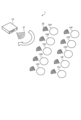
- FIG. 1 is a diagram illustrating an example of the configuration of a communication system according to the first embodiment.
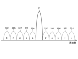
- FIG. 2 is a diagram showing the signal levels of a transmission signal and a reflected signal in an ideal environment according to the first embodiment.
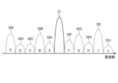
- FIG. 3 is a diagram showing the signal levels of a transmission signal and a reflected signal in an actual environment according to the first embodiment.
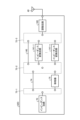
- FIG. 4 is a block diagram showing an example of the configuration of the slave unit according to the first embodiment.
- FIG. 5 is a diagram showing an example of the configuration of the impedance rotation circuit according to the first embodiment.
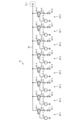
- FIG. 6 is a diagram illustrating an example of the configuration of the impedance circuit according to the first embodiment.
- FIG. 7 is a diagram illustrating an example of the configuration of a matching circuit according to the first embodiment.
- FIG. 1 is a diagram illustrating an example of the configuration of a communication system according to the first embodiment.
- FIG. 2 is a diagram showing the signal levels of a transmission signal and a reflected signal in
- FIG. 8 is a diagram showing the signal level of the reflected signal according to the first embodiment.
- FIG. 9 is a diagram showing the signal level of the reflected signal according to the first embodiment.
- FIG. 10 is a diagram showing an example of the configuration of an impedance rotation circuit according to the second embodiment.
- FIG. 11 is a diagram showing a first configuration example of a resistive attenuator according to the second embodiment.
- FIG. 12 is a diagram showing a second configuration example of the resistive attenuator according to the second embodiment.
- FIG. 13 is a diagram showing an example of the configuration of an impedance rotation circuit according to the third embodiment.
- FIG. 14 is a diagram for explaining the parasitic capacitance of a switch.
- FIG. 15 is a diagram showing an example of the configuration of a parasitic cancellation circuit according to the third embodiment.
- FIG. 16 is a diagram illustrating an example of the configuration of an impedance rotation circuit according to the fourth embodiment.
- FIG. 17 is a diagram illustrating an example of the configuration of an impedance conversion circuit according to the fourth embodiment.
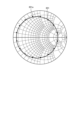
- FIG. 18 is a Smith chart showing the impedance of the impedance rotation circuit according to the first example of the fourth embodiment.
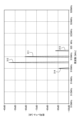
- FIG. 19 is a diagram illustrating the signal level of a reflected signal of the impedance rotation circuit according to the first example of the fourth embodiment.
- FIG. 20 is a Smith chart showing the impedance of the impedance rotation circuit according to the second example of the fourth embodiment.
- FIG. 21 is a diagram illustrating the signal level of a reflected signal of the impedance rotation circuit according to the second example of the fourth embodiment.
- FIG. 22 is a Smith chart showing the impedance of the impedance rotation circuit according to the third example of the fourth embodiment.
- FIG. 23 is a diagram illustrating the signal level of a reflected signal of the impedance rotation circuit according to the third example of the fourth embodiment.
- FIG. 24 is a Smith chart showing the impedance of the impedance rotation circuit according to the fourth example of the fourth embodiment.
- FIG. 25 is a diagram illustrating the signal level of a reflected signal of an impedance rotation circuit according to the fourth example of the fourth embodiment.
- FIG. 26 is a Smith chart showing the impedance of an impedance rotation circuit according to a fifth example of the fourth embodiment.
- FIG. 27 is a diagram illustrating the signal level of a reflected signal of an impedance rotation circuit according to a fifth example of the fourth embodiment.
- FIG. 28 is a Smith chart showing the impedance of an impedance rotation circuit according to the sixth example of the fourth embodiment.
- FIG. 29 is a diagram illustrating the signal level of a reflected signal of an impedance rotation circuit according to the sixth example of the fourth embodiment.
- FIG. 30 is a diagram showing the relationship between the impedance and the signal level of the impedance rotation circuit according to the fourth embodiment.
- FIG. 31 is a diagram showing an example of the configuration of an impedance rotation circuit according to the fifth embodiment.
- FIG. 32 is a diagram illustrating an example of the configuration of an adjustment circuit according to the fifth embodiment.
- FIG. 33 is a diagram showing the signal level of a reflected signal according to a comparative example of the fifth embodiment.
- FIG. 34 is a Smith chart showing the impedance of the impedance rotation circuit according to the fifth embodiment.
- FIG. 35 is a diagram showing the signal level of a reflected signal of the impedance rotation circuit according to the fifth embodiment.
- FIG. 36 is a diagram showing a configuration example of an impedance rotation circuit according to the sixth embodiment.
- FIG. 1 is a diagram showing a configuration example of a communication system according to the first embodiment.
- communication system 1 includes parent unit 10, child unit 12A, child unit 12B, child unit 12C, child unit 12D, child unit 12E, child unit 12F, child unit 12G, child unit 12H, child unit 12I, and child unit 12J.
- Child unit 12A When there is no need to distinguish child unit 12A from child unit 12J, they are collectively referred to as child unit 12.
- Communication system 1 is a system that performs data communication using a backscatter method.
- Parent unit 10 and child unit 12 are wireless communication devices that perform backscatter communication.
- child unit 12 is configured to transmit to parent unit 10 a reflected signal 22 that reflects a transmission signal 21 transmitted by the parent unit.
- (signal level) 2 is a diagram showing the signal levels of a transmission signal and a reflected signal in an ideal environment according to the first embodiment.
- Waveform 31 shows the signal level of the transmission signal 21 transmitted by the parent unit.
- Waveforms 32A to 32J show the signal levels of the reflected signals 22 reflected by the child units 12A to 12J, respectively.
- the signal levels of the reflected signals 22 reflected by the child units 12A to 12J are ideally the same. In an ideal environment, each of the child units 12A to 12J can properly communicate with the parent unit 10 without being disturbed by the reflected signals 22 reflected by the other child units 12.
- FIG. 3 is a diagram showing the signal levels of the transmission signal and the reflected signal in the first embodiment in a real environment.
- the signal levels of the reflected signal 22 reflected by each of the slave units 12A and 12J may differ.
- the slave unit 12J is assigned to a communication channel that the slave unit 12E has suppressed by making it a single sideband.
- the reflected signal 22 of the slave unit 12E may become an interference signal that makes it difficult for the slave unit 12J to communicate with the master unit 10. In such a case, it is required to appropriately suppress the signal level of the reflected signal 22 of the slave unit 12E.
- Fig. 4 is a block diagram showing an example of the configuration of the slave unit according to the first embodiment.
- the handset 12 includes an antenna 40, a switch (SW) 41, a receiving circuit 42, a transmitting circuit 43, a control unit 44, and a sensor 45.
- SW switch
- the switch 41 is configured to be able to switch the path between the antenna 40 and the receiving circuit 42 and the transmitting circuit 43.
- the switch 41 electrically connects the antenna 40 to the receiving circuit 42.
- the switch 41 electrically connects the antenna 40 to the transmitting circuit 43.
- the receiving circuit 42 receives the transmission signal from the parent unit 10 received by the antenna 40.
- the receiving circuit 42 is configured to perform various reception processes on the transmission signal.
- the transmission circuit 43 is a circuit that generates a reflected signal (also called a backscatter signal) transmitted by the antenna 40.
- the transmission circuit 43 includes a CPU interface (I/F) 60, a control circuit 61, an impedance rotation circuit 62, and a PLL (Phase Looked Loop) circuit 63.
- the control circuit 61 is configured to control the impedance rotation circuit 62.
- the control circuit 61 controls the impedance rotation circuit 62 based on a control signal input from the control unit 44 via the CPU interface 60, an oscillation signal input from the PLL circuit 63, and the like.
- the control circuit 61 is configured to change the impedance of the impedance rotation circuit 62.
- the control circuit 61 changes the impedance of the impedance rotation circuit 62 to control the reflection coefficient of the output terminal on the antenna 40 side to rotate in the complex plane.
- the control circuit 61 for example, reduces the USB (Upper Side Band) signal or LSB (Lower Side Band) signal for the carrier signal of the backscatter signal to realize a single sideband.
- the impedance rotation circuit 62 is disposed at the front end of the child device 12.
- the impedance rotation circuit 62 is configured to reflect the transmission signal sent by the child device 12 as a backscatter signal and perform backscatter communication.
- the impedance rotation circuit 62 includes multiple impedance circuits, each of which has a different impedance.
- the control circuit 61 and the impedance rotation circuit 62 are a type of transmission circuit of the present disclosure.
- the PLL circuit 63 is configured to generate an oscillation signal of a predetermined frequency.
- the PLL circuit 63 generates the oscillation signal in accordance with a control signal from the control unit 44.
- the PLL circuit 63 is configured to output the generated oscillation signal to the control circuit 61.
- the control unit 44 is configured to control each part of the handset 12.
- the control unit 44 may be realized, for example, by an information processing device such as a CPU (Central Processing Unit) or an MPU (Micro Processing Unit), and a storage device such as a RAM (Random Access Memory) or a ROM (Read Only Memory).
- the control unit 44 may be realized, for example, by an integrated circuit such as an ASIC (Application Specific Integrated Circuit) or an FPGA (Field Programmable Gate Array).
- the control unit 44 may be realized by a combination of hardware and software.
- the sensor 45 includes various sensors.
- the sensor 45 may include, for example, a speed sensor, a vibration sensor, an acceleration sensor, a gyro sensor, a rotation angle sensor, an angular velocity sensor, a geomagnetic sensor, a magnet sensor, a temperature sensor, a humidity sensor, an air pressure sensor, a light sensor, an illuminance sensor, a UV sensor, a gas sensor, a gas concentration sensor, an atmosphere sensor, a level sensor, an odor sensor, a pressure sensor, an air pressure sensor, a contact sensor, a wind sensor, an infrared sensor, a human presence sensor, a displacement sensor, an image sensor, a weight sensor, a smoke sensor, a leakage sensor, a vital sensor, a battery remaining amount sensor, and an ultrasonic sensor.
- the sensor 45 may include a GNSS (Global Navigation Satellite System) sensor that acquires the current position information of the handset 12.
- GNSS Global Navigation Satellite System
- Fig. 5 is a diagram showing a configuration example of the impedance rotation circuit according to the first embodiment.
- the impedance rotation circuit 62 includes impedance circuits 70-1, ..., impedance circuits 70-n (n is an integer equal to or greater than 2), switches 72-1, 72-2, 72-3, a matching circuit 73, wiring 74, and a phase shifter 75. Different reflection coefficients are set for the impedance circuits 70-1 to 70-n. When it is not necessary to distinguish between the impedance circuits 70-1 to 70-n, they are collectively referred to as impedance circuits 70. In other words, the impedance rotation circuit 62 includes multiple impedance circuits 70 with different reflection coefficients.
- the impedance circuits 70-1 to 70-n are electrically connected to the matching circuit 73 by the switch 72-1.
- the switch 72-1 is, for example, a transistor, but is not limited to this.
- the switch 72-1 is controlled by the control circuit 61.
- the switch 72-1 is configured to selectively connect any one of the impedance circuits 70-1 to 70-n to the matching circuit 73.
- the control circuit 61 can control the reflection coefficient by controlling the switch 72-1 to switch the impedance circuit 70 to be connected.
- the impedance circuit 70 adds impedance to the impedance rotation circuit 62.
- FIG. 6 is a diagram showing an example of the configuration of the impedance circuit according to the first embodiment.
- the impedance circuit 70 includes a first circuit 80-1, a second circuit 80-2, a third circuit 80-3, a fourth circuit 80-4, a fifth circuit 80-5, a sixth circuit 80-6, a seventh circuit 80-7, and an eighth circuit 80-8.
- the first circuit 80-1 to the eighth circuit 80-8 are electrically connected by a signal line 85.
- the first circuit 80-1 includes a signal source 81-1, a switch element 82-1, a resistor element 83-1, and a capacitor 84-1.
- the signal source 81-1 indicates a signal source of a control signal from the control circuit 61 for controlling the switch element 82-1.
- One end of the signal source 81-1 is electrically connected to a reference potential.
- the reference potential is, for example, but is not limited to, ground.
- the signal source 81-1 outputs a control signal for controlling the on and off states of the switch element 82-1 to the switch element 82-1.
- One end of the switch element 82-1 is electrically connected to a signal line 85.
- One end of the switch element 82-1 is electrically connected to one end of the resistor element 83-1.
- the second circuit 80-2 includes a signal source 81-2, a switch element 82-2, a resistive element 83-2, and a capacitor 84-2.
- the signal source 81-2 indicates a signal source of a control signal from the control circuit 61 for controlling the switch element 82-2. One end of the signal source 81-2 is electrically connected to a reference potential. The signal source 81-2 outputs a control signal for controlling the on state and off state of the switch element 82-2 to the switch element 82-2. One end of the switch element 82-2 is electrically connected to a signal line 85. One end of the switch element 82-2 is electrically connected to one end of the resistive element 83-2. The other end of the resistive element 83-2 is electrically connected to one end of the capacitor 84-2.
- the other end of the capacitor 84-2 is electrically connected to the reference potential.
- the switch element 82-2 When the switch element 82-2 is in the on state, the resistive element 83-2 and the capacitor 84-2 are electrically connected to the signal line 85.
- the impedance of the impedance circuit 70 changes depending on the resistance value of the resistive element 83-2 and the capacitance value of the capacitor 84-2.
- the third circuit 80-3 includes a signal source 81-3, a switch element 82-3, a resistor element 83-3, and a capacitor 84-3.
- the signal source 81-3 indicates a signal source of a control signal from the control circuit 61 for controlling the switch element 82-3.
- One end of the signal source 81-3 is electrically connected to a reference potential.
- the signal source 81-3 outputs a control signal for controlling the on state and off state of the switch element 82-3 to the switch element 82-3.
- One end of the switch element 82-3 is electrically connected to a signal line 85.
- One end of the switch element 82-3 is electrically connected to one end of the resistor element 83-3.
- the other end of the resistor element 83-3 is electrically connected to one end of the capacitor 84-3.
- the other end of the capacitor 84-3 is electrically connected to the reference potential.
- the switch element 82-3 When the switch element 82-3 is in the on state, the resistor element 83-3 and the capacitor 84-3 are electrically connected to the signal line 85.
- the impedance of the impedance circuit 70 changes depending on the resistance value of the resistive element 83-3 and the capacitance value of the capacitor 84-3.
- the fourth circuit 80-4 includes a signal source 81-4, a switch element 82-4, a resistive element 83-4, and a capacitor 84-4.
- the signal source 81-4 indicates a signal source of a control signal from the control circuit 61 for controlling the switch element 82-4.
- One end of the signal source 81-4 is electrically connected to a reference potential.
- the signal source 81-4 outputs a control signal for controlling the on state and off state of the switch element 82-4 to the switch element 82-4.
- One end of the switch element 82-4 is electrically connected to a signal line 85.
- One end of the switch element 82-4 is electrically connected to one end of the resistive element 83-4.
- the other end of the resistive element 83-4 is electrically connected to one end of the capacitor 84-4.
- the other end of the capacitor 84-4 is electrically connected to the reference potential.
- the switch element 82-4 When the switch element 82-4 is in the on state, the resistive element 83-4 and the capacitor 84-4 are electrically connected to the signal line 85.
- the impedance of the impedance circuit 70 changes depending on the resistance value of the resistive element 83-4 and the capacitance value of the capacitor 84-4.
- the fifth circuit 80-5 includes a signal source 81-5, a switch element 82-5, a resistive element 83-5, and a capacitor 84-5.
- the signal source 81-5 indicates a signal source of a control signal from the control circuit 61 for controlling the switch element 82-5.
- One end of the signal source 81-5 is electrically connected to a reference potential.
- the signal source 81-5 outputs a control signal for controlling the on state and off state of the switch element 82-5 to the switch element 82-5.
- One end of the switch element 82-5 is electrically connected to a signal line 85.
- One end of the switch element 82-5 is electrically connected to one end of the resistive element 83-5.
- the other end of the resistive element 83-5 is electrically connected to one end of the capacitor 84-5.
- the other end of the capacitor 84-5 is electrically connected to the reference potential.
- the switch element 82-5 When the switch element 82-5 is in the on state, the resistive element 83-5 and the capacitor 84-5 are electrically connected to the signal line 85.
- the impedance of the impedance circuit 70 changes depending on the resistance value of the resistor element 83-5 and the capacitance value of the capacitor 84-5.
- the sixth circuit 80-6 includes a signal source 81-6, a switch element 82-6, a resistor element 83-6, and a capacitor 84-6.
- the signal source 81-6 indicates a signal source of a control signal from the control circuit 61 for controlling the switch element 82-6.
- One end of the signal source 81-6 is electrically connected to a reference potential.
- the signal source 81-6 outputs a control signal for controlling the on state and off state of the switch element 82-6 to the switch element 82-6.
- One end of the switch element 82-6 is electrically connected to a signal line 85.
- One end of the switch element 82-6 is electrically connected to one end of the resistor element 83-6.
- the other end of the resistor element 83-6 is electrically connected to one end of the capacitor 84-6.
- the other end of the capacitor 84-6 is electrically connected to the reference potential.
- the switch element 82-6 When the switch element 82-6 is in the on state, the resistor element 83-6 and the capacitor 84-6 are electrically connected to the signal line 85.
- the impedance of the impedance circuit 70 changes depending on the resistance value of the resistor element 83-6 and the capacitance value of the capacitor 84-6.
- the seventh circuit 80-7 includes a signal source 81-7, a switch element 82-7, a resistor element 83-7, and a capacitor 84-7.
- the signal source 81-7 indicates a signal source of a control signal from the control circuit 61 for controlling the switch element 82-7.
- One end of the signal source 81-7 is electrically connected to a reference potential.
- the signal source 81-7 outputs a control signal for controlling the on state and off state of the switch element 82-7 to the switch element 82-7.
- One end of the switch element 82-7 is electrically connected to a signal line 85.
- One end of the switch element 82-7 is electrically connected to one end of the resistor element 83-7.
- the other end of the resistor element 83-7 is electrically connected to one end of the capacitor 84-7.
- the other end of the capacitor 84-7 is electrically connected to the reference potential.
- the switch element 82-7 is in the on state, the resistor element 83-7 and the capacitor 84-7 are electrically connected to the signal line 85.
- the impedance of the impedance circuit 70 changes depending on the resistance value of the resistor element 83-7 and the capacitance value of the capacitor 84-7.
- the eighth circuit 80-8 includes a signal source 81-8, a switch element 82-8, a resistor element 83-8, and a capacitor 84-8.
- the signal source 81-8 indicates a signal source of a control signal from the control circuit 61 for controlling the switch element 82-8.
- One end of the signal source 81-8 is electrically connected to a reference potential.
- the signal source 81-8 outputs a control signal for controlling the on state and off state of the switch element 82-8 to the switch element 82-8.
- One end of the switch element 82-8 is electrically connected to a signal line 85.
- One end of the switch element 82-8 is electrically connected to one end of the resistor element 83-8.
- the other end of the resistor element 83-8 is electrically connected to one end of the capacitor 84-8.
- the other end of the capacitor 84-8 is electrically connected to the reference potential.
- the switch element 82-8 is in the on state, the resistor element 83-8 and the capacitor 84-8 are electrically connected to the signal line 85.
- the impedance of the impedance circuit 70 changes depending on the resistance value of the resistor element 83-8 and the capacitance value of the capacitor 84-8.
- the control circuit 61 is configured to selectively change the impedance rotation circuit and rotate the reflection coefficient on the polar chart by selectively controlling the on and off states of each of the switch elements 82-1 to 82-8.
- the control circuit 61 can control the attenuation of the reflected signal by selectively switching the connection between the impedance circuits 70-1 to 70-n and the matching circuit 73 to control the reflection coefficient ⁇ .
- the reflection coefficient ⁇ is 1, the attenuation of the reflected signal is 0 dB (decibels).
- the reflection coefficient ⁇ is 0.9, the attenuation of the reflected signal is 0.91 dB.
- the reflection coefficient ⁇ is 0.8, the attenuation of the reflected signal is 1.93 dB.
- the reflection coefficient ⁇ is 0.7, the attenuation of the reflected signal is 3.10 dB.
- the attenuation of the reflected signal is 4.44 dB.
- the attenuation of the reflected signal is 6.02 dB.
- the attenuation of the reflected signal is 7.96 dB.
- the attenuation of the reflected signal is 10.46 [dB].
- the reflection coefficient ⁇ is 0.2, the attenuation of the reflected signal is 13.98 [dB].
- the reflection coefficient ⁇ is 0.1, the attenuation of the reflected signal is 20 [dB].
- the matching circuit 73 is a circuit that matches the output impedance of the impedance circuit 70 with the input impedance of the antenna 40.
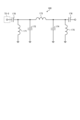
- FIG. 7 is a diagram showing an example of the configuration of a matching circuit according to the first embodiment.
- the matching circuit 73 includes a capacitor 91, an inductor 92, and a capacitor 93.
- One end of the capacitor 91 is electrically connected to the switch 72-1 and one end of the inductor 92.
- the other end of the capacitor 91 is electrically connected to a reference potential.
- One end of the capacitor 93 is electrically connected to the switch 72-2 and the other end of the inductor 92.
- the other end of the capacitor 93 is electrically connected to the reference potential.
- the matching circuit 73 is selectively connected to the wiring 74 or the phase shifter 75 by the switch 72-2.
- the switch 72-2 is, for example, a transistor, but is not limited to this.
- the switch 72-2 is controlled by the control circuit 61.
- the wiring 74 or the phase shifter 75 is selectively connected to the input terminal of the antenna 40 by the switch 72-3.
- the switch 72-3 is controlled by the control circuit 61.
- the phase shifter 75 has the same configuration as the matching circuit 73 shown in FIG. 7, so a description thereof is omitted.
- the phase shifter 75 shifts the phase of the input signal by 90° and outputs it.
- the signal output from the matching circuit 73 is input to the input terminal of the antenna 40 without any change in phase.
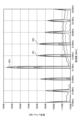
- FIG. 8 is a diagram showing the signal level of the reflected signal according to the first embodiment.
- the horizontal axis indicates frequency [MHz (megahertz)], and the vertical axis indicates signal level [dB].
- FIG. 8 shows the signal levels of carrier signal 201, USB signal 202, and LSB signal 203.
- USB signal 202 is suppressed compared to LSB signal 203.
- impedance rotation circuit 62 realizes a single sideband of the LSB signal.
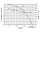
- FIG. 9 is a diagram showing the signal level of the reflected signal according to the first embodiment.
- the horizontal axis indicates the reflection coefficient
- the left vertical axis indicates the signal level difference [dB]
- the right vertical axis indicates the signal level [dB].
- the reflection coefficient ⁇ is set to 0.8 as a reference.
- Graph 211 indicates the signal level of the reflected signal
- graph 210 indicates the difference between the signal level at the corresponding reflection coefficient ⁇ and the signal level at the reflection coefficient ⁇ of 0.8.
- the signal level of the reflected signal can be controlled by controlling the reflection coefficient.
- the reflection coefficient of the impedance rotation circuit 62 can be controlled to control the amount of attenuation of the reflected signal. This allows the first embodiment to appropriately achieve a single sideband.
- Fig. 10 is a diagram showing a configuration example of the impedance rotation circuit according to the second embodiment.
- the impedance rotation circuit 62A includes impedance circuits 70-1 to 70-n, switches 72-1, 72-2, 72-3, and 72-4, a matching circuit 73, wiring 74, a phase shifter 75, wiring 76, and resistive attenuators 77-1 to 77-n.
- resistive attenuators 77 When there is no need to distinguish between resistive attenuators 77-1 to 77-n, they are collectively referred to as resistive attenuators 77.
- the impedance rotation circuit 62A differs from the impedance rotation circuit 62 shown in FIG. 5 in that it includes switch 72-3 and resistive attenuator 77.
- the wiring 74 or the phase shifter 75 is selectively connected to either the wiring 76 or the resistive attenuators 77-1 to 77-n by the switch 72-3.
- the switch 72-3 is, for example, a transistor, but is not limited to this.
- the switch 72-3 is controlled by the control circuit 61.
- the resistive attenuator 77 is configured to attenuate the signal level of the reflected signal.
- the resistive attenuators 77-1 to 77-n are each configured to have a different reflected signal attenuation amount. They are configured not to attenuate the reflected signal of the wiring 76. That is, the control circuit 61 can control the attenuation amount by controlling the switch 72-4 to switch the resistive attenuator 77 to be connected. In the second embodiment, the provision of the resistive attenuator 77 allows the reflected signal to be attenuated more appropriately.
- FIG. 11 is a diagram showing a first configuration example of the resistive attenuator according to the second embodiment.
- the resistive attenuator 77 according to the first configuration example includes resistive elements 101, 102, and 103.
- One end of resistive element 101 is electrically connected to switch 72-3 and one end of resistive element 103.
- the other end of resistive element 101 is electrically connected to a reference potential.
- One end of resistive element 102 is electrically connected to switch 72-4 and the other end of resistive element 103.
- the attenuation [dB] of the reflected signal of resistive attenuator 77 changes depending on the resistance values of resistive elements 101, 102, and 103.
- the attenuation becomes 2 [dB].
- the resistance values of the resistive elements 101 and 102 are set to 220.97 [ ⁇ ] and the resistance value of the resistive element 103 is set to 23.85 [ ⁇ ]
- the attenuation is 4 [dB].
- the resistance values of the resistive elements 101 and 102 are set to 150.48 [ ⁇ ] and the resistance value of the resistive element 103 is set to 37.35 [ ⁇ ]
- the attenuation is 6 [dB].
- the attenuation is 8 [dB].
- the resistance values of the resistive elements 101 and 102 are set to 96.25 [ ⁇ ] and the resistance value of the resistive element 103 is set to 71.15 [ ⁇ ]
- the attenuation is 10 [dB].
- the resistance values of the resistive elements 101 and 102 are 83.54 [ ⁇ ] and the resistance value of the resistive element 103 is 93.25 [ ⁇ ]
- the attenuation is 12 [dB].
- the attenuation is 14 [dB].
- the resistance values of the resistive elements 101 and 102 are 68.83 [ ⁇ ] and the resistance value of the resistive element 103 is 150.78 [ ⁇ ]
- the attenuation is 16 [dB].
- the resistance values of the resistive elements 101 and 102 are 64.40 [ ⁇ ] and the resistance value of the resistive element 103 is 195.43 [ ⁇ ]
- the attenuation is 18 [dB].
- the attenuation is 20 [dB].
- FIG. 12 is a diagram showing a second configuration example of the resistive attenuator according to the second embodiment.
- the resistive attenuator 77 according to the second configuration example includes resistive elements 111, 112, and 113.
- One end of the resistive element 111 is electrically connected to the switch 72-3.
- the other end of the resistive element 111 is electrically connected to one end of the resistive element 112 and one end of the resistive element 113.
- the other end of the resistive element 112 is electrically connected to the switch 72-4.
- the other end of the resistive element 113 is electrically connected to a reference potential.
- the attenuation [dB] of the reflected signal of the resistive attenuator 77 changes depending on the resistance values of the resistive elements 111, 112, and 113. For example, by setting the resistance values of the resistive elements 111 and 112 to 5.73 [ ⁇ ] and the resistance value of the resistive element 113 to 215.24 [ ⁇ ], the attenuation becomes 2 [dB]. For example, by setting the resistance value of the resistive element 111 and the resistive element 112 to 11.31 [ ⁇ ] and the resistance value of the resistive element 113 to 104.83 [ ⁇ ], the attenuation is 4 [dB].
- the attenuation is 6 [dB].
- the attenuation is 8 [dB].
- the attenuation is 10 [dB].
- the attenuation becomes 12 [dB].
- the attenuation becomes 14 [dB].
- the attenuation becomes 16 [dB].
- the attenuation becomes 18 [dB].
- the resistance value of resistor element 111 and resistor element 112 is set to 38.82 [ ⁇ ] and the resistance value of the resistive element 113 to 12.79 [ ⁇ ]
- the attenuation is 20 [dB].
- Graph 210 in FIG. 9 shows the signal level when the reflection coefficient ⁇ of the impedance circuit 70 is 0.2 and the attenuation of the resistive attenuator 77 is 10 dB.
- graph 210 shows, the attenuation of the reflected signal from the impedance circuit 70 with a reflection coefficient ⁇ of 0.2 and the resistive attenuator 77 with an attenuation of 10 dB is greater than the attenuation of the reflected signal from the impedance circuit 70 with a reflection coefficient ⁇ of 0.2.
- resistive attenuators 77-1 to 77-n are connected in parallel. This is because if resistive attenuators 77-1 to 77-n are connected in series, they will be susceptible to the parasitic capacitance of switches 72-3 and 72-4, and there is a risk that the amount of attenuation of the reflected signal will change. Therefore, in the second embodiment, it is preferable to connect resistive attenuators 77-1 to 77-n in parallel in order to make it easier to take into account the influence of the parasitic capacitance of switches 72-3 and 72-4.
- the channel width (W) of each of the transistors constituting the switches 72-1 to 72-4 is the same. It is also preferable that the channel length (L) of each of the transistors constituting the switches 72-1 to 72-4 is the same. If the channel width and channel length of each of the transistors constituting the switches 72-1 to 72-4 are different, the impedance rotation circuit 62A may not be able to obtain the desired characteristics due to the variation in parasitic capacitance. Therefore, in the second embodiment, the channel width and channel length of each of the transistors constituting the switches 72-1 to 72-4 are made the same, thereby reducing the variation in parasitic capacitance. This makes it easier to consider the influence of the parasitic capacitance of the switches 72-1 to 72-4.
- the impedance rotation circuit 62A includes the impedance circuit 70 and the resistive attenuator 77, so that the reflected signal can be attenuated more appropriately. This allows the second embodiment to more appropriately achieve a single sideband.
- Fig. 13 is a diagram showing a configuration example of the impedance rotation circuit according to the third embodiment.
- the impedance rotation circuit 62B includes impedance circuits 70-1 to 70-n, switches 72-1, 72-2, 72-3, 72-4, 72-5, matching circuit 73, wiring 74, phase shifter 75, wiring 76, resistive attenuators 77-1 to 77-n, parasitic cancellation circuits 78-1, 78-2, and 78-3.
- the impedance rotation circuit 62B differs from the impedance rotation circuit 62A shown in FIG. 10 in that it includes switch 72-5 and parasitic cancellation circuits 78-1 to 78-3. When it is not necessary to distinguish between the parasitic cancellation circuits 78-1 to 78-3, they may be collectively referred to as the parasitic cancellation circuits 78.
- Switches 72-1 to 72-5 are configured so that the channel width and channel length of each transistor are the same.
- Control circuit 61 controls the on and off states of switches 72-1 to 72-5.
- a parasitic cancellation circuit is provided to cancel the parasitic capacitance of each switch 72, thereby reducing the effect of the parasitic capacitance of each switch 72.
- One end of the parasitic cancellation circuit 78-1 is electrically connected to the switch 72-1.
- the other end of the parasitic cancellation circuit 78-1 is electrically connected to one end of the matching circuit 73.
- the switch 72-1 selectively connects the impedance circuits 70-1 to 70-n to the parasitic cancellation circuit 78-1.
- One end of the parasitic cancellation circuit 78-2 is electrically connected to the switch 72-3.
- the other end of the parasitic cancellation circuit 78-2 is electrically connected to the switch 72-4.
- the switch 72-3 selectively connects the wiring 74 or the phase shifter 75 to the parasitic cancellation circuit 78-2.
- the switch 72-4 selectively connects the parasitic cancellation circuit 78-2 to the wiring 76 or the resistive attenuators 77-1 to 77-n.
- One end of the parasitic cancellation circuit 78-3 is electrically connected to the switch 72-5.
- the other end of the parasitic cancellation circuit 78-3 is electrically connected to the input terminal of the antenna 40.
- the switch 72-5 selectively connects the wiring 76 or the resistive attenuators 77-1 to 77-n to the parasitic cancellation circuit 78-3.
- the parasitic cancellation circuits 78-1 to 78-3 each have the same configuration.
- the configuration of the parasitic cancellation circuit 78 will be described later.
- FIG. 14 is a diagram for explaining the parasitic capacitance of a switch.
- the switch 72 is, for example, a transistor.
- the switch 72 has a parasitic capacitance 120 between the gate terminal and the source terminal.
- the switch 72 has a parasitic capacitance 121 between the gate terminal and the drain terminal.
- the switch 72 has a parasitic capacitance 122 between the source terminal and the drain terminal.
- FIG. 15 is a diagram showing an example of the configuration of a parasitic cancellation circuit according to the third embodiment.
- the parasitic cancellation circuit 78 includes a capacitor 131, a capacitor 132, and an inductor 133.
- One end of the capacitor 131 is electrically connected to an external device.
- the other end of the capacitor 131 is electrically connected to one end of the capacitor 132 and one end of the inductor 133.
- the other end of the capacitor 132 is electrically connected to the external device.
- the other end of the inductor 133 is electrically connected to a reference potential.
- one end of the capacitor 131 is electrically connected to the drain terminal of the switch 72-1, and the other end of the capacitor 132 is electrically connected to the input terminal of the matching circuit 73.
- one end of the capacitor 131 is electrically connected to the drain terminal of the switch 72-3, and the other end of the capacitor 132 is electrically connected to the source terminal of the switch 72-4.
- the capacitor 131 is electrically connected to the drain terminal of the switch 72-5, and the other end of the capacitor 132 is electrically connected to the input terminal of the antenna 40.
- the effects of parasitic capacitance 120, parasitic capacitance 121, and parasitic capacitance 122 can be cancelled out by connecting parasitic cancellation circuit 78 to switch 72. This allows the third embodiment to more appropriately achieve a single sideband.
- Fig. 16 is a diagram showing a configuration example of the impedance rotation circuit according to the fourth embodiment.
- the impedance rotation circuit 62C includes an impedance circuit 70, a switch 72-1, a switch 72-2, a switch 72-3, wiring 74, a phase shifter 75, wiring 140, and impedance conversion circuits 141-1 to 141-n.
- impedance conversion circuits 141 When there is no need to distinguish between the impedance conversion circuits 141-1 to 141-n, they are collectively referred to as the impedance conversion circuits 141.
- the impedance rotation circuit 62C differs from the impedance rotation circuit 62 shown in FIG. 5 in that it does not include a matching circuit 73, it includes only one impedance circuit 70, and it includes multiple impedance conversion circuits 141.
- the wiring 140 or any one of the impedance conversion circuits 141-1 to 141-n is selectively connected to the wiring 74 or the phase shifter 75 by the switch 72-2.
- the wiring 140 or any one of the impedance conversion circuits 141-1 to 141-n is selectively connected to the antenna 40 by the switch 72-3.
- the impedance conversion circuit 141 is a circuit that converts impedance.
- the impedance conversion circuits 141-1 to 141-n each have a different amount of impedance conversion.
- the impedance of the impedance circuit 70 is 50 [ ⁇ ].
- the impedance conversion circuit 141 converts, for example, 50 [ ⁇ ] to 10 [ ⁇ ], 25 [ ⁇ ], 200 [ ⁇ ], 500 [ ⁇ ], 1000 [ ⁇ ], etc.
- the wiring 140 is configured not to convert impedance. In this embodiment, the amount of impedance conversion can be controlled by controlling the switches 72-2 and 72-3 to selectively connect to the wiring 140 or one of the impedance conversion circuits 141-1 to 141-n.
- FIG. 17 is a diagram showing an example of the configuration of an impedance conversion circuit according to the fourth embodiment.
- the impedance conversion circuit 141 includes a capacitor 151, an inductor 152, and a capacitor 153.
- One end of the capacitor 151 is electrically connected to the switch 72-2 and one end of the inductor 152.
- One end of the capacitor 153 is electrically connected to the switch 72-3 and the inductor 152.
- the amount of impedance conversion by the impedance conversion circuit 141 varies depending on the capacitance values of the capacitors 151 and 153 and the inductance of the inductor 152. For example, by setting the capacitance value of the capacitor 151 to 8.67 pF (picofarads), the capacitance value of the capacitor 153 to 11.63 pF, and the inductance of the inductor 152 to 3.79 nH (nanohenries), the impedance conversion circuit 141 can convert the impedance from 50 ⁇ to 10 ⁇ .
- the impedance conversion circuit 141 can convert the impedance from 50 ⁇ to 25 ⁇ .
- the impedance conversion circuit 141 can convert the impedance from 50 [ ⁇ ] to 200 [ ⁇ ].
- the impedance conversion circuit 141 can convert the impedance from 50 [ ⁇ ] to 500 [ ⁇ ].
- the impedance conversion circuit 141 can convert the impedance from 50 [ ⁇ ] to 1000 [ ⁇ ].
- Fig. 18 is a Smith chart showing the impedance of the impedance rotation circuit according to the first example of the fourth embodiment.
- Fig. 19 is a diagram showing the signal level of the reflected signal of the impedance rotation circuit according to the first example of the fourth embodiment.
- the horizontal axis represents frequency [MHz]
- the vertical axis represents signal level [dB].
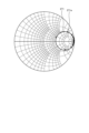
- the impedance of the impedance rotation circuit 62C is 50 [ ⁇ ]. That is, in the first example of the fourth embodiment, the impedance is not converted. As shown in FIG. 18, the impedance of the impedance rotation circuit 62C rotates along a circle 221. Points 221a indicate the impedance values that the impedance rotation circuit 62C can take. There are 16 points 221a at approximately equal intervals on the circle 221. As shown in FIG. 19, the signal level of the carrier signal 222 is approximately -79.87 [dB], the signal level of the LSB signal 223 is approximately -43.58 [dB], and the signal level of the USB signal 224 is -89.93 [dB]. The difference between the signal level of the LSB signal 223 and the signal level of the USB signal 224 is 43.35 [dB].
- Fig. 20 is a Smith chart showing the impedance of the impedance rotation circuit according to the second example of the fourth embodiment.
- Fig. 21 is a diagram showing the signal level of the reflected signal of the impedance rotation circuit according to the second example of the fourth embodiment.
- the horizontal axis represents frequency [MHz]
- the vertical axis represents signal level [dB].
- the impedance of the impedance rotation circuit 62C is 10 [ ⁇ ]. That is, in the second example of the fourth embodiment, the impedance is converted from 50 [ ⁇ ] to 10 [ ⁇ ] using the impedance conversion circuit 141. As shown in FIG. 20, the impedance of the impedance rotation circuit 62C rotates along a circle 231. Points 231a indicate the impedance values that the impedance rotation circuit 62C can take. On the circle 231, there are 16 points 221a at non-equidistant intervals. As shown in FIG.
- the signal level of the carrier signal 232 is about -45.09 [dB]
- the signal level of the LSB signal 233 is about -48.71 [dB]
- the signal level of the USB signal 234 is -85.03 [dB].
- the difference between the signal level of the LSB signal 233 and the signal level of the USB signal 234 is 36.32 [dB].
- Fig. 22 is a Smith chart showing the impedance of the impedance rotation circuit according to the third example of the fourth embodiment.
- Fig. 23 is a diagram showing the signal level of the reflected signal of the impedance rotation circuit according to the third example of the fourth embodiment.
- the horizontal axis represents frequency [MHz]
- the vertical axis represents signal level [dB].
- the impedance of the impedance rotation circuit 62C is 25 [ ⁇ ]. That is, in the third example of the fourth embodiment, the impedance is converted from 50 [ ⁇ ] to 25 [ ⁇ ] using the impedance conversion circuit 141. As shown in FIG. 22, the impedance of the impedance rotation circuit 62C rotates along a circle 241. Points 241a indicate the impedance values that the impedance rotation circuit 62C can take. There are 16 points 241a at non-equidistant intervals on the circle 241. As shown in FIG.
- the signal level of the carrier signal 242 is about -51.61 [dB]
- the signal level of the LSB signal 243 is about -44.74 [dB]
- the signal level of the USB signal 244 is -83.94 [dB].
- the difference between the signal level of the LSB signal 243 and the signal level of the USB signal 244 is 39.20 [dB].
- Fig. 24 is a Smith chart showing the impedance of the impedance rotation circuit according to the fourth example of the fourth embodiment.
- Fig. 25 is a diagram showing the signal level of the reflected signal of the impedance rotation circuit according to the fourth example of the fourth embodiment.
- the horizontal axis represents frequency [MHz]
- the vertical axis represents signal level [dB].
- the impedance of the impedance rotation circuit 62C is 200 [ ⁇ ]. That is, in the fourth example of the fourth embodiment, the impedance is converted from 50 [ ⁇ ] to 200 [ ⁇ ] using the impedance conversion circuit 141. As shown in FIG. 24, the impedance of the impedance rotation circuit 62C rotates along a circle 251. Points 251a indicate the impedance values that the impedance rotation circuit 62C can take. There are 16 points 251a at non-equidistant intervals on the circle 251. As shown in FIG.
- the signal level of the carrier signal 252 is about -45.81 [dB]
- the signal level of the LSB signal 253 is about -47.91 [dB]
- the signal level of the USB signal 254 is -90.59 [dB].
- the difference between the signal level of the LSB signal 253 and the signal level of the USB signal 254 is 42.68 [dB].
- Fig. 26 is a Smith chart showing the impedance of the impedance rotation circuit according to the fifth example of the fourth embodiment.
- Fig. 27 is a diagram showing the signal level of the reflected signal of the impedance rotation circuit according to the fifth example of the fourth embodiment.
- the horizontal axis represents frequency [MHz]
- the vertical axis represents signal level [dB].
- the impedance of the impedance rotation circuit 62C is 500 [ ⁇ ]. That is, in the fifth example of the fourth embodiment, the impedance is converted from 50 [ ⁇ ] to 500 [ ⁇ ] using the impedance conversion circuit 141. As shown in FIG. 26, the impedance of the impedance rotation circuit 62C rotates along a circle 261. Points 261a indicate the impedance values that the impedance rotation circuit 62C can take. There are 16 points 261a at non-equidistant intervals on the circle 261. As shown in FIG.
- the signal level of the carrier signal 262 is about -43.04 [dB]
- the signal level of the LSB signal 263 is about -53.72 [dB]
- the signal level of the USB signal 264 is -96.66 [dB].
- the difference between the signal level of the LSB signal 263 and the signal level of the USB signal 264 is 42.94 [dB].
- Fig. 28 is a Smith chart showing the impedance of the impedance rotation circuit according to the sixth example of the fourth embodiment.
- Fig. 29 is a diagram showing the signal level of the reflected signal of the impedance rotation circuit according to the sixth example of the fourth embodiment.
- the horizontal axis represents frequency [MHz]
- the vertical axis represents signal level [dB].
- the impedance of the impedance rotation circuit 62C is 1000 [ ⁇ ]. That is, in the sixth example of the fourth embodiment, the impedance is converted from 50 [ ⁇ ] to 1000 [ ⁇ ] using the impedance conversion circuit 141. As shown in FIG. 28, the impedance of the impedance rotation circuit 62C rotates along a circle 271. Points 271a indicate the impedance values that the impedance rotation circuit 62C can take. There are 16 points 271a at non-equidistant intervals on the circle 271. As shown in FIG.
- the signal level of the carrier signal 272 is about -43.32 [dB]
- the signal level of the LSB signal 273 is about -58.95 [dB]
- the signal level of the USB signal 254 is -98.97 [dB].
- the difference between the signal level of the LSB signal 273 and the signal level of the USB signal 274 is 40.02 [dB].
- the amount of attenuation of the reflected signal can be controlled by converting the impedance of the impedance rotation circuit 62C.
- FIG. 30 is a diagram showing the relationship between the impedance and signal level of the impedance rotation circuit according to the fourth embodiment.
- the horizontal axis indicates the impedance conversion value of the impedance rotation circuit 62C
- the left vertical axis indicates the signal level difference [dB]
- the right vertical axis indicates the signal level [dB].
- the impedance of the impedance rotation circuit 62C is set to 50 [ ⁇ ] as the reference.
- Graph 281 indicates the signal level of the reflected signal
- graph 280 indicates the difference between the signal level at the corresponding impedance and the signal level at an impedance of 50 [ ⁇ ].
- the signal level of the reflected signal can be controlled by converting the impedance of the impedance rotation circuit 62C.
- the fourth embodiment can control the signal level of the reflected signal by using multiple impedance conversion circuits 141. This allows the fourth embodiment to appropriately achieve a single sideband.
- FIG. 31 is a diagram showing a configuration example of the impedance rotation circuit according to the fifth embodiment.
- the impedance rotation circuit 62D includes an impedance circuit 70, a switch 72-1, a switch 72-2, a switch 72-3, a wiring 74, a phase shifter 75, a wiring 140, impedance conversion circuits 141-1 to 141-n, and an adjustment circuit 160.
- the impedance rotation circuit 62D differs from the impedance rotation circuit 62C shown in FIG. 16 in that it includes an adjustment circuit 160.
- the signal level of the reflected signal is adjusted using multiple impedance conversion circuits 141, the signal level of the harmonic signal will increase.
- the harmonic signal and the reflected signal may interfere with each other, making it impossible to communicate properly. This is because the intervals between the points 231a indicating the impedance are no longer constant due to the impedance conversion, as shown in Figure 20.
- the signal level of the harmonic signal in the 916 MHz band will increase, as shown in Figure 21. Therefore, in the fifth embodiment, the signal level of the harmonic signal is reduced using an adjustment circuit 160.
- One end of the adjustment circuit 160 is connected to the wiring 140 or one of the impedance conversion circuits 141-1 to 141-n by the switch 72-3.
- the other end of the adjustment circuit 160 is connected to the input terminal of the antenna 40.
- FIG. 32 is a diagram showing an example of the configuration of an adjustment circuit according to the fifth embodiment.
- the adjustment circuit 160 includes a capacitor 170, an inductor 171, a capacitor 172, an inductor 173, a capacitor 174, an inductor 175, and a capacitor 176.
- One end of the capacitor 170 is electrically connected to the switch 72-3.
- the other end of the capacitor 170 is electrically connected to one end of the inductor 171.
- inductor 171 One end of inductor 171 is electrically connected to the other end of capacitor 170 and one end of capacitor 172. The other end of inductor 171 is electrically connected to a reference potential.
- capacitor 172 One end of capacitor 172 is electrically connected to one end of inductor 171 and one end of inductor 173. The other end of capacitor 172 is electrically connected to the reference potential.
- inductor 173 One end of inductor 173 is electrically connected to one end of capacitor 172. The other end of inductor 173 is electrically connected to one end of capacitor 174.
- capacitor 174 is electrically connected to the other end of inductor 173 and one end of inductor 175. The other end of capacitor 174 is electrically connected to the reference potential.
- inductor 175 is electrically connected to one end of capacitor 174 and one end of capacitor 176. The other end of inductor 175 is electrically connected to the reference potential.
- One end of the capacitor 176 is electrically connected to one end of the inductor 175.
- the other end of the capacitor 176 is electrically connected to the input terminal of the antenna 40.
- FIG. 33 is a diagram showing the signal level of a reflected signal according to the comparative example of the fifth embodiment.
- the horizontal axis indicates frequency [MHz]
- the vertical axis indicates signal level [dB].
- the impedance is converted from 50 [ ⁇ ] to 25 [ ⁇ ] using the impedance conversion circuit 141. That is, the point 241a shown in FIG. 22 indicates the impedance of the impedance rotation circuit according to the comparative example of the fifth embodiment.
- FIG. 33 is a diagram showing the signal level of a reflected signal according to the comparative example of the fifth embodiment.
- the horizontal axis indicates frequency [MHz]
- the vertical axis indicates signal level [dB].
- the impedance is converted from 50 [ ⁇ ] to 25 [ ⁇ ] using the impedance conversion circuit 141. That is, the point 241a shown in FIG. 22 indicates the impedance of the impedance rotation circuit according to the comparative example of the fifth embodiment.
- FIG. 22 indicates the impedance of the impedance rotation
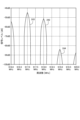
- the signal levels of the carrier signal 291, the LSB signal 292, the USB signal 293, the harmonic signal 294, the harmonic signal 295, and the harmonic signal 296 are higher than the signal level of USB signal 293. Therefore, there is a risk that the reflected signal of another child device 12 will interfere with harmonic signal 294, harmonic signal 295, or harmonic signal 296.
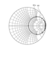
- the impedance of the impedance rotation circuit 62D is 25 ⁇ . That is, in the fifth embodiment, the impedance is converted from 50 ⁇ to 25 ⁇ using the impedance conversion circuit 141. As shown in FIG. 34, the impedance of the impedance rotation circuit 62D rotates along a circle 301. Points 301a indicate the impedance values that the impedance rotation circuit 62D can take. As shown in FIG. 34, unlike the points 241a shown in FIG. 22, the circle 301 includes 16 points 301a at equal intervals. That is, in the fifth embodiment, by using the adjustment circuit 160, the impedance rotation circuit 62D can maintain a constant interval between the points 301a even if the impedance is converted using the impedance conversion circuit 141.
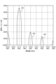
- FIG. 35 shows the signal levels of carrier signal 311, LSB signal 312, USB signal 313, and harmonic signal 314.
- a single sideband of LSB signal 312 is realized with the signal level of USB signal 313 suppressed.
- the signal level of harmonic signal 314 is lower than the signal level of USB signal 313. That is, in the fifth embodiment, impedance rotation circuit 62D can suppress the signal level of the harmonic signal by using adjustment circuit 160. Therefore, it is possible to prevent the reflected signal of another child device 12 from interfering with harmonic signal 314.
- the fifth embodiment can control the signal level of the harmonic signal by using the adjustment circuit 160. This allows the fifth embodiment to appropriately achieve a single sideband.
- Fig. 36 is a diagram showing a configuration example of the impedance rotation circuit according to the sixth embodiment.
- the impedance rotation circuit 62E includes an impedance circuit 70, a switch 72-1, a switch 72-2, a switch 72-3, a switch 72-4, a wiring 74, a phase shifter 75, a parasitic cancellation circuit 78-1, a parasitic cancellation circuit 78-2, a parasitic cancellation circuit 78-3, a wiring 140, impedance conversion circuits 141-1 to 141-n, and an adjustment circuit 160.
- the impedance rotation circuit 62E differs from the impedance rotation circuit 62D shown in FIG. 31 in that it includes a switch 72-4, a parasitic cancellation circuit 78-1, a parasitic cancellation circuit 78-2, and a parasitic cancellation circuit 78-3.
- One end of the parasitic cancellation circuit 78-1 is electrically connected to the output terminal of the impedance circuit 70.
- the other end of the parasitic cancellation circuit 78-1 is electrically connected to one end of the switch 72-1.
- the switch 72-1 selectively connects the wiring 74 or the phase shifter 75 to the parasitic cancellation circuit 78-1.
- the parasitic cancellation circuit 78-1 can cancel the effect of the parasitic capacitance of the switch 72-1.
- One end of the parasitic cancellation circuit 78-3 is electrically connected to the switch 72-3.
- the other end of the parasitic cancellation circuit 78-3 is electrically connected to the input terminal of the adjustment circuit 160.
- the switch 72-3 selectively connects the wiring 140 or the impedance conversion circuit 141-1 to the impedance conversion circuit 141-n and the parasitic cancellation circuit 78-3.
- the parasitic cancellation circuit 78-3 can cancel the effect of the parasitic capacitance of the switch 72-3.
- the effect of the parasitic capacitance of each switch can be cancelled by connecting a parasitic cancellation circuit to each switch. This allows the sixth embodiment to more appropriately achieve a single sideband.
Landscapes
- Engineering & Computer Science (AREA)
- Computer Networks & Wireless Communication (AREA)
- Signal Processing (AREA)
- Networks Using Active Elements (AREA)
Abstract
Description
[通信システム]
図1を用いて、第1実施形態に係る通信システムの構成例について説明する。図1は、第1実施形態に係る通信システムの構成例を示す図である。
図2は、第1実施形態に係る送信信号および反射信号の理想環境下における信号レベルを示す図である。波形31は、親機が送信した送信信号21の信号レベルを示す。波形32Aから波形32Jは、それぞれ、子機12Aから子機12Jが反射した反射信号22の信号レベルを示す。図2に示すように、子機12Aから子機12Jが反射した反射信号22の信号レベルは、理想的には、同じである。理想環境下では、子機12Aから子機12Jは、それぞれ、他の子機12が反射した反射信号22に妨害されることなく、親機10と適切に通信することができる。
図4を用いて、第1実施形態に係る子機の構成例について説明する。図4は、第1実施形態に係る子機の構成例を示すブロック図である。
図5を用いて、第1実施形態に係るインピーダンス回転回路の構成例について説明する。図5は、第1実施形態に係るインピーダンス回転回路の構成例を示す図である。
(インピーダンス回転回路)
図10を用いて、第2実施形態に係るインピーダンス回転回路の構成例について説明する。図10は、第2実施形態に係るインピーダンス回転回路の構成例を示す図である。
(インピーダンス回転回路)
図13を用いて、第3実施形態に係るインピーダンス回転回路の構成例について説明する。図13は、第3実施形態に係るインピーダンス回転回路の構成例を示す図である。
(インピーダンス回転回路)
図16を用いて、第4実施形態に係るインピーダンス回転回路の構成例について説明する。図16は、第4実施形態に係るインピーダンス回転回路の構成例を示す図である。
図18は、第4実施形態の第1の例に係るインピーダンス回転回路のインピーダンスを示すスミスチャートである。図19は、第4実施形態の第1の例に係るインピーダンス回転回路の反射信号の信号レベルを示す図である。図19は、横軸が周波数[MHz]を示し、縦軸が信号レベル[dB]を示す。
図20は、第4実施形態の第2の例に係るインピーダンス回転回路のインピーダンスを示すスミスチャートである。図21は、第4実施形態の第2の例に係るインピーダンス回転回路の反射信号の信号レベルを示す図である。図21は、横軸が周波数[MHz]を示し、縦軸が信号レベル[dB]を示す。
図22は、第4実施形態の第3の例に係るインピーダンス回転回路のインピーダンスを示すスミスチャートである。図23は、第4実施形態の第3の例に係るインピーダンス回転回路の反射信号の信号レベルを示す図である。図23は、横軸が周波数[MHz]を示し、縦軸が信号レベル[dB]を示す。
図24は、第4実施形態の第4の例に係るインピーダンス回転回路のインピーダンスを示すスミスチャートである。図25は、第4実施形態の第4の例に係るインピーダンス回転回路の反射信号の信号レベルを示す図である。図25は、横軸が周波数[MHz]を示し、縦軸が信号レベル[dB]を示す。
図26は、第4実施形態の第5の例に係るインピーダンス回転回路のインピーダンスを示すスミスチャートである。図27は、第4実施形態の第5の例に係るインピーダンス回転回路の反射信号の信号レベルを示す図である。図27は、横軸が周波数[MHz]を示し、縦軸が信号レベル[dB]を示す。
図28は、第4実施形態の第6の例に係るインピーダンス回転回路のインピーダンスを示すスミスチャートである。図29は、第4実施形態の第6の例に係るインピーダンス回転回路の反射信号の信号レベルを示す図である。図29は、横軸が周波数[MHz]を示し、縦軸が信号レベル[dB]を示す。
(インピーダンス回転回路)
図31を用いて、第5実施形態に係るインピーダンス回転回路の構成例について説明する。図31は、第5実施形態に係るインピーダンス回転回路の構成例を示す図である。
ここで、第5実施形態の比較例について説明する。図33は、第5実施形態の比較例に係る反射信号の信号レベルを示す図である。図33は、横軸が周波数[MHz]を示し、縦軸が信号レベル[dB]を示す。第5実施形態の比較例では、インピーダンス変換回路141を用いて、インピーダンスを50[Ω]から25[Ω]に変換しているものとする。すなわち、図22に示す点241aが第5実施形態の比較例に係るインピーダンス回転回路のインピーダンスを示す。図33には、キャリア信号291と、LSB信号292と、USB信号293と、高調波信号294と、高調波信号295と、高調波信号296と、の信号レベルが示されている。図33に示す例では、USB信号293の信号レベルが抑圧された、LSB信号292のシングルサイドバンドが実現されている。図33に示すように、第5実施形態の比較例では、高調波信号294、高調波信号295、および高調波信号296の信号レベルは、USB信号293の信号レベルと比較して高い。そのため、他の子機12の反射信号と、高調波信号294、高調波信号295、または高調波信号296とが干渉してしまうおそれがある。
図34は、第5実施形態に係るインピーダンス回転回路のインピーダンスを示すスミスチャートである。図35は、第5実施形態に係るインピーダンス回転回路の反射信号の信号レベルを示す図である。図35は、横軸が周波数[MHz]を示し、縦軸が信号レベル[dB]を示す。
(インピーダンス回転回路)
図36を用いて、第6実施形態に係るインピーダンス回転回路の構成例について説明する。図36は、第6実施形態に係るインピーダンス回転回路の構成例を示す図である。
10 親機
12 子機
40 アンテナ
41 スイッチ
42 受信回路
43 送信回路
44 制御部
45 センサ
60 CPUインターフェース
61 制御回路
62,62A,62B,62C,62D,62E インピーダンス回転回路
70 インピーダンス回路
72-1,72-2,72-3,72-4,72-5 スイッチ
73 整合回路
74,76,140 配線
75 移相器
77 抵抗減衰器
78-1,78-2,78-3 寄生打消回路
141 インピーダンス変換回路
Claims (11)
- 所定の反射係数が設定され、アンテナに接続するように構成されたインピーダンス回路を備えるインピーダンス回転回路と、
前記インピーダンス回転回路の反射係数を制御して、複素平面において、反射係数を回転するように制御する制御回路と、を含み、
前記制御回路は、前記インピーダンス回転回路の反射係数に応じて、反射信号の信号レベルを制御する、
伝送回路。 - 前記インピーダンス回転回路は、反射係数の異なる複数の前記インピーダンス回路を備え、
前記アンテナと、複数の前記インピーダンス回路とは、第1スイッチにより接続され、
前記制御回路は、前記第1スイッチを制御し、前記アンテナと、複数の前記インピーダンス回路との接続を切り替えることで、複素平面において、反射係数を回転するように制御する、
請求項1に記載の伝送回路。 - 前記インピーダンス回転回路は、複数の前記インピーダンス回路と、前記アンテナとの間において抵抗減衰器を備える、
請求項2に記載の伝送回路。 - 前記抵抗減衰器は、減衰値の異なる複数の抵抗減衰器が並列に接続して構成され、
複数の前記抵抗減衰器と、前記アンテナおよび複数の前記インピーダンス回路とは、第2スイッチにより接続され、
前記制御回路は、前記第2スイッチを制御することで、複数の前記抵抗減衰器と、前記アンテナおよび複数の前記インピーダンス回路との接続を制御する、
請求項3に記載の伝送回路。 - 前記第1スイッチと、前記第2スイッチとは、大きさが同じである、
請求項4に記載の伝送回路。 - 前記インピーダンス回転回路は、
前記第1スイッチに接続された第1寄生打消回路と、
前記第2スイッチに接続された第2寄生打消回路と、を備える、
請求項4に記載の伝送回路。 - 前記インピーダンス回転回路は、前記インピーダンス回路と、前記アンテナとの間において、変換量の異なる複数のインピーダンス変換回路を備え、
複数の前記インピーダンス変換回路と、前記インピーダンス回路および前記アンテナとは、第1スイッチにより接続され、
前記制御回路は、前記第1スイッチを制御し、複数の前記インピーダンス変換回路と、前記インピーダンス回路および前記アンテナとの接続を切り替えることで、複素平面において、反射係数を回転するように制御する、
請求項1に記載の伝送回路。 - 複数の前記インピーダンス変換回路は、前記インピーダンス回路との接続を切り替えた際のインピーダンスの間隔が一定になるように構成されている、
請求項7に記載の伝送回路。 - 前記インピーダンス回転回路は、
複数の前記インピーダンス変換回路と、前記アンテナとの間において、前記インピーダンス回路との接続を切り替えた際のインピーダンスの間隔が一定になるように構成された調整回路を備え、
複数の前記インピーダンス変換回路と、前記アンテナとは、第2スイッチで接続されている、
請求項7に記載の伝送回路。 - 前記第1スイッチと、前記第2スイッチとは、大きさが同じである、
請求項9に記載の伝送回路。 - 前記インピーダンス回転回路は、
前記第1スイッチに接続された第1寄生打消回路と、
前記第2スイッチに接続された際2寄生打消回路と、を備える、
請求項10に記載の伝送回路。
Priority Applications (1)
| Application Number | Priority Date | Filing Date | Title |
|---|---|---|---|
| JP2025506913A JP7851001B2 (ja) | 2023-03-15 | 2024-03-13 | 伝送回路 |
Applications Claiming Priority (2)
| Application Number | Priority Date | Filing Date | Title |
|---|---|---|---|
| JP2023-041322 | 2023-03-15 | ||
| JP2023041322 | 2023-03-15 |
Publications (1)
| Publication Number | Publication Date |
|---|---|
| WO2024190844A1 true WO2024190844A1 (ja) | 2024-09-19 |
Family
ID=92755259
Family Applications (1)
| Application Number | Title | Priority Date | Filing Date |
|---|---|---|---|
| PCT/JP2024/009896 Ceased WO2024190844A1 (ja) | 2023-03-15 | 2024-03-13 | 伝送回路 |
Country Status (2)
| Country | Link |
|---|---|
| JP (1) | JP7851001B2 (ja) |
| WO (1) | WO2024190844A1 (ja) |
Citations (5)
| Publication number | Priority date | Publication date | Assignee | Title |
|---|---|---|---|---|
| US20210012071A1 (en) * | 2018-06-27 | 2021-01-14 | Telefonaktiebolaget Lm Ericsson (Publ) | A network control entity, an access point and methods therein for enabling access to wireless tags in a wireless communications network |
| WO2022024488A1 (ja) * | 2020-07-30 | 2022-02-03 | 新日本無線株式会社 | センサインターフェース回路及びセンサモジュール |
| JP2022056139A (ja) * | 2020-09-29 | 2022-04-08 | 国立大学法人東京工業大学 | 伝送回路 |
| JP2022056169A (ja) * | 2020-09-29 | 2022-04-08 | 国立大学法人東京工業大学 | 合成回路 |
| JP2022056911A (ja) * | 2020-09-30 | 2022-04-11 | 国立大学法人東京工業大学 | 伝送回路 |
-
2024
- 2024-03-13 WO PCT/JP2024/009896 patent/WO2024190844A1/ja not_active Ceased
- 2024-03-13 JP JP2025506913A patent/JP7851001B2/ja active Active
Patent Citations (5)
| Publication number | Priority date | Publication date | Assignee | Title |
|---|---|---|---|---|
| US20210012071A1 (en) * | 2018-06-27 | 2021-01-14 | Telefonaktiebolaget Lm Ericsson (Publ) | A network control entity, an access point and methods therein for enabling access to wireless tags in a wireless communications network |
| WO2022024488A1 (ja) * | 2020-07-30 | 2022-02-03 | 新日本無線株式会社 | センサインターフェース回路及びセンサモジュール |
| JP2022056139A (ja) * | 2020-09-29 | 2022-04-08 | 国立大学法人東京工業大学 | 伝送回路 |
| JP2022056169A (ja) * | 2020-09-29 | 2022-04-08 | 国立大学法人東京工業大学 | 合成回路 |
| JP2022056911A (ja) * | 2020-09-30 | 2022-04-11 | 国立大学法人東京工業大学 | 伝送回路 |
Also Published As
| Publication number | Publication date |
|---|---|
| JP7851001B2 (ja) | 2026-04-24 |
| JPWO2024190844A1 (ja) | 2024-09-19 |
Similar Documents
| Publication | Publication Date | Title |
|---|---|---|
| US20100315121A1 (en) | Adaptive termination | |
| US8742818B2 (en) | Adaptive clock signal generator with noise immunity capability | |
| JP2016506663A (ja) | リコンフィギュラブルマルチバンドアンテナ | |
| US10132918B2 (en) | Antenna apparatus and array antenna apparatus for radar | |
| KR20150034811A (ko) | 가변 이득 트랜스-컨덕턴스 스테이지를 구비한 튜닝가능한 적응형 필터 | |
| WO2022070672A1 (ja) | 伝送回路 | |
| US20240074319A1 (en) | Driver circuitry for piezoelectric transducers | |
| JP7851001B2 (ja) | 伝送回路 | |
| JP2016001865A (ja) | 検波校正回路及び送信装置 | |
| US11209272B2 (en) | Circuit device, physical quantity measurement device, electronic apparatus, and vehicle | |
| WO2005104379A1 (ja) | 受信装置、送信装置、及び無線システム | |
| CN112840576A (zh) | 一种温度补偿电路和相控阵装置 | |
| TW202207650A (zh) | 分時雙工(tdd)天線系統 | |
| JP2019168330A (ja) | 半導体装置 | |
| JP2017225124A (ja) | 高速パルス変調システム | |
| JP3891043B2 (ja) | 複数アンテナ対応インピーダンス整合装置を搭載した無線機 | |
| JP2013201757A (ja) | 増幅器におけるインピーダンス調整 | |
| CN114095679B (zh) | 视频发送电路及其信号延迟补偿方法 | |
| US20230198485A1 (en) | Bidirectional amplifier including matching circuits having symmetrical structure and communication device including the same | |
| TWI783717B (zh) | 前饋式回波消除裝置 | |
| TWI779671B (zh) | 具有訊號校正機制的數位至類比轉換裝置及方法 | |
| WO2024190845A1 (ja) | 伝送回路 | |
| KR102315039B1 (ko) | 채널 보정 가능한 다중 채널 송수신 장치 및 방법 | |
| WO2024190732A1 (ja) | 伝送回路 | |
| TWI355811B (en) | Apparatus with tunable filter and related adjustin |
Legal Events
| Date | Code | Title | Description |
|---|---|---|---|
| 121 | Ep: the epo has been informed by wipo that ep was designated in this application |
Ref document number: 24770947 Country of ref document: EP Kind code of ref document: A1 |
|
| ENP | Entry into the national phase |
Ref document number: 2025506913 Country of ref document: JP Kind code of ref document: A |
|
| WWE | Wipo information: entry into national phase |
Ref document number: 2025506913 Country of ref document: JP |
|
| NENP | Non-entry into the national phase |
Ref country code: DE |
|
| 122 | Ep: pct application non-entry in european phase |
Ref document number: 24770947 Country of ref document: EP Kind code of ref document: A1 |