WO2024190426A1 - 半導体装置および車両 - Google Patents
半導体装置および車両 Download PDFInfo
- Publication number
- WO2024190426A1 WO2024190426A1 PCT/JP2024/007410 JP2024007410W WO2024190426A1 WO 2024190426 A1 WO2024190426 A1 WO 2024190426A1 JP 2024007410 W JP2024007410 W JP 2024007410W WO 2024190426 A1 WO2024190426 A1 WO 2024190426A1
- Authority
- WO
- WIPO (PCT)
- Prior art keywords
- lead
- semiconductor device
- electrode
- conductive member
- wire
- Prior art date
- Legal status (The legal status is an assumption and is not a legal conclusion. Google has not performed a legal analysis and makes no representation as to the accuracy of the status listed.)
- Ceased
Links
Images










Classifications
-
- H—ELECTRICITY
- H10—SEMICONDUCTOR DEVICES; ELECTRIC SOLID-STATE DEVICES NOT OTHERWISE PROVIDED FOR
- H10W—GENERIC PACKAGES, INTERCONNECTIONS, CONNECTORS OR OTHER CONSTRUCTIONAL DETAILS OF DEVICES COVERED BY CLASS H10
- H10W72/00—Interconnections or connectors in packages
-
- H—ELECTRICITY
- H10—SEMICONDUCTOR DEVICES; ELECTRIC SOLID-STATE DEVICES NOT OTHERWISE PROVIDED FOR
- H10W—GENERIC PACKAGES, INTERCONNECTIONS, CONNECTORS OR OTHER CONSTRUCTIONAL DETAILS OF DEVICES COVERED BY CLASS H10
- H10W72/00—Interconnections or connectors in packages
- H10W72/071—Connecting or disconnecting
-
- H—ELECTRICITY
- H10—SEMICONDUCTOR DEVICES; ELECTRIC SOLID-STATE DEVICES NOT OTHERWISE PROVIDED FOR
- H10W—GENERIC PACKAGES, INTERCONNECTIONS, CONNECTORS OR OTHER CONSTRUCTIONAL DETAILS OF DEVICES COVERED BY CLASS H10
- H10W90/00—Package configurations
Definitions
- This disclosure relates to a semiconductor device and a vehicle equipped with the semiconductor device.
- Patent Document 1 discloses an example of a conventional semiconductor device.
- the semiconductor device disclosed in this document comprises a number of leads, a semiconductor element, and a number of conductive members.
- the number of conductive members include a metal clip and a wire.
- the metal clip is joined to an electrode formed on the upper surface of the semiconductor element and to a lead.
- the wire is joined to an electrode formed on the upper surface of the semiconductor element and to another lead. In such a semiconductor device, it is required to pass a larger current.
- An object of the present disclosure is to provide a semiconductor device that is an improvement over conventional devices.
- an object of the present disclosure is to provide a semiconductor device that is suitable for passing a large current.
- the semiconductor device provided by the first aspect of the present disclosure includes a first lead having a base, a semiconductor element mounted on one side of the base in the thickness direction and having a first electrode arranged on one side of the thickness direction, a second lead arranged at a distance from the base on one side of a first direction perpendicular to the thickness direction, a third lead arranged at a distance from the base on one side of the first direction, a conductive member electrically connected to the first electrode and the second lead, and a first wire.
- the third lead is arranged at a distance from the second lead in a second direction perpendicular to both the thickness direction and the first direction.
- the first wire is electrically connected to the conductive member and the third lead.
- the vehicle provided by the second aspect of the present disclosure is equipped with a power conversion device that includes a semiconductor device according to the first aspect of the present disclosure.
- the above configuration makes it possible to provide a semiconductor device with a structure that is favorable for passing large currents.
- FIG. 1 is a perspective view showing a semiconductor device according to a first embodiment of the present disclosure.
- FIG. 2 is a partial perspective view showing the semiconductor device according to the first embodiment of the present disclosure.
- FIG. 3 is a plan view showing the semiconductor device according to the first embodiment of the present disclosure.
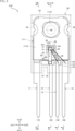
- FIG. 4 is a partial plan view showing the semiconductor device according to the first embodiment of the present disclosure.
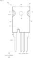
- FIG. 5 is a bottom view showing the semiconductor device according to the first embodiment of the present disclosure.
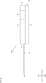
- FIG. 6 is a side view showing the semiconductor device according to the first embodiment of the present disclosure.
- FIG. 7 is a front view showing the semiconductor device according to the first embodiment of the present disclosure.
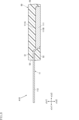
- FIG. 8 is a cross-sectional view taken along line VIII-VIII in FIG. FIG.
- FIG. 9 is a cross-sectional view taken along line IX-IX in FIG.
- FIG. 10 is a cross-sectional view taken along line XX in FIG.
- FIG. 11 is a cross-sectional view taken along line XI-XI in FIG.
- FIG. 12 is a partially enlarged view of a part of FIG.
- FIG. 13 is a partially enlarged view of a part of FIG.
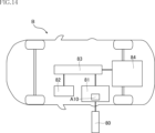
- FIG. 14 is a schematic diagram of a vehicle including the semiconductor device according to the first embodiment of the present disclosure.
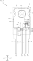
- FIG. 15 is a partial plan view showing a semiconductor device according to a first modification of the first embodiment.
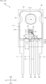
- FIG. 16 is a partial plan view showing a semiconductor device according to a second modification of the first embodiment.
- FIG. 15 is a partial plan view showing a semiconductor device according to a first modification of the first embodiment.
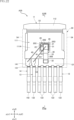
- FIG. 17 is a partial plan view showing a semiconductor device according to a third modification of the first embodiment.
- FIG. 18 is a partial plan view showing a semiconductor device according to a fourth modification of the first embodiment.
- FIG. 19 is a partial plan view showing a semiconductor device according to a fifth modification of the first embodiment.
- FIG. 20 is a partial plan view showing a semiconductor device according to a second embodiment of the present disclosure.
- FIG. 21 is a partial plan view showing a semiconductor device according to a first modification of the second embodiment.
- FIG. 22 is a partial plan view showing a semiconductor device according to a third embodiment of the present disclosure.
- FIG. 23 is a cross-sectional view taken along line XXIII-XXIII in FIG.
- an object A is formed on an object B" and “an object A is formed on an object B” include “an object A is formed directly on an object B” and “an object A is formed on an object B with another object interposed between the object A and the object B” unless otherwise specified.
- an object A is disposed on an object B” and “an object A is disposed on an object B” include “an object A is disposed directly on an object B” and “an object A is disposed on an object B with another object interposed between the object A and the object B" unless otherwise specified.
- an object A is located on an object B includes “an object A is located on an object B in contact with an object B” and “an object A is located on an object B with another object interposed between the object A and the object B” unless otherwise specified.
- an object A overlaps an object B when viewed in a certain direction includes “an object A overlaps the entire object B” and “an object A overlaps a part of an object B.”
- a surface A faces in direction B is not limited to the case where the angle of surface A with respect to direction B is 90 degrees, but also includes the case where surface A is tilted with respect to direction B.
- First embodiment 1 to 13 show a semiconductor device according to a first embodiment of the present disclosure.
- the application of A10 of this embodiment is not limited in any way, and it is used in electronic devices equipped with a power conversion circuit, such as a DC-DC converter.
- the semiconductor device A10 includes a first lead 11, a second lead 12, a third lead 13, a fourth lead 14, a semiconductor element 20, a conductive member 30, a first wire 41, a second wire 42, and a sealing resin 50.
- FIG. 1 is a perspective view showing the semiconductor device A10.
- FIG. 2 is a partial perspective view showing the semiconductor device A10.
- FIG. 3 is a plan view showing the semiconductor device A10.
- FIG. 4 is a partial plan view showing the semiconductor device A10.
- the outer shape of the sealing resin 50 is shown by an imaginary line (two-dot chain line).
- FIG. 5 is a bottom view showing the semiconductor device A10.
- FIG. 6 is a side view showing the semiconductor device A10.
- FIG. 7 is a front view showing the semiconductor device A10.
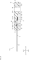
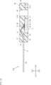
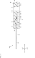
- FIG. 8 is a cross-sectional view taken along line VIII-VIII in FIG. 4.
- FIG. 9 is a cross-sectional view taken along line IX-IX in FIG. 4.
- FIG. 10 is a cross-sectional view taken along line X-X in FIG. 4.
- FIG. 11 is a cross-sectional view taken along line XI-XI in FIG. 4.
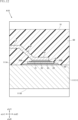
- FIG. 12 is a partial enlarged view of a part of FIG. 9.
- FIG. 13 is a partial enlarged view of a part of FIG. 11.
- the first wire 41 is omitted in FIG. 9.
- the thickness direction of the semiconductor element 20 of the present disclosure is defined as the "thickness direction z.”
- One direction perpendicular to the thickness direction z is called the “first direction x.”
- the direction perpendicular to both the thickness direction z and the first direction x is called the "second direction y.”
- the first lead 11 has a base 111 and a terminal portion 112.
- the first lead 11 is a conductive member on which the semiconductor element 20 is mounted and which forms part of the conductive path between the semiconductor element 20 and a wiring board (not shown) on which the semiconductor device A10 is mounted, etc.
- the first lead 11 includes, for example, copper (Cu) or a copper alloy.
- the first lead 11 may also have a surface metal layer (not shown).
- the surface metal layer includes, for example, silver (Ag), nickel (Ni), etc.
- the base 111 has a first main surface 111A, a first back surface 111B, and a through hole 111C.
- the first main surface 111A faces the z1 side in the thickness direction z.
- the first back surface 111B faces the z2 side in the z direction.
- the through hole 111C penetrates the base 111 in the thickness direction z.
- the shape of the through hole 111C is not limited in any way, and in the illustrated example, it is circular when viewed in the thickness direction z (in a plan view).
- the terminal portion 112 is connected to the base portion 111 and extends to the x1 side in the first direction x.
- the base portion 111 and the terminal portion 112 are electrically conductive to each other.
- a portion of the terminal portion 112 is covered with the sealing resin 50.
- the portion of the terminal portion 112 covered with the sealing resin 50 is bent when viewed in the second direction y.
- the surface of the portion of the terminal portion 112 exposed from the sealing resin 50 may be plated with, for example, tin (Sn).
- the second lead 12 is separated from the first lead 11 and is disposed on the y2 side of the second direction y with respect to the terminal portion 112 of the first lead 11.
- the second lead 12 is disposed on the x1 side of the first direction x with respect to the base portion 111 of the first lead 11.
- the second lead 12 is electrically connected to the semiconductor element 20 via the conductive member 30.
- the second lead 12 has a pad portion 121 and a terminal portion 122.
- the pad portion 121 is covered with a sealing resin 50.
- the pad portion 121 may be plated with, for example, silver (Ag) or tin (Sn).
- the terminal portion 122 is connected to the pad portion 121.
- a portion of the terminal portion 122 is covered with the sealing resin 50, and another portion is exposed from the sealing resin 50.
- the terminal portion 122 extends in the first direction x, for example, parallel to the terminal portion 112.
- the surface of the terminal portion 122 may be plated with, for example, tin (Sn).
- the third lead 13 is separated from the first lead 11 and the second lead 12 and is disposed at a distance from the second lead 12 on the y2 side in the second direction y.
- the third lead 13 is adjacent to the second lead 12 in the second direction y.
- the third lead 13 is disposed at a distance from the base 111 on the x1 side in the first direction x.
- the third lead 13 is electrically connected to the semiconductor element 20 via the first wire 41 and the conductive member 30.
- the third lead 13 has a pad portion 131 and a terminal portion 132.
- the pad portion 131 is covered with sealing resin 50.
- the pad portion 131 may be plated with, for example, silver (Ag) or tin (Sn).
- the terminal portion 132 is connected to the pad portion 131. A portion of the terminal portion 132 is covered with sealing resin 50, and another portion is exposed from the sealing resin 50. Terminal portion 132 extends in the first direction x, for example, parallel to terminal portion 112 and terminal portion 122.
- the surface of terminal portion 132 may be plated with, for example, tin (Sn).
- the fourth lead 14 is separated from the first lead 11, the second lead 12 and the third lead 13, and is disposed at a distance from the third lead 13 on the y2 side in the second direction y.
- the fourth lead 14 is located on the opposite side of the second lead 12 from the third lead 13 in the second direction y.
- the fourth lead 14 is also disposed at a distance from the base 111 on the x1 side in the first direction x.
- the fourth lead 14 is electrically connected to the semiconductor element 20 via the second wire 42.
- the fourth lead 14 has a pad portion 141 and a terminal portion 142.
- the pad portion 141 is covered with the sealing resin 50.
- the pad portion 141 may be plated with, for example, silver (Ag) or tin (Sn).
- the terminal portion 142 is connected to the pad portion 141. A portion of the terminal portion 142 is covered with the sealing resin 50, and another portion is exposed from the sealing resin 50. Terminal portion 142 extends in the first direction x, for example, parallel to terminal portion 112, terminal portion 122, and terminal portion 132.
- the surface of terminal portion 142 may be plated with, for example, tin (Sn).
- the semiconductor element 20 is mounted on the first main surface 111A of the base 111, as shown in Figures 2, 4, and 9 to 13.
- the specific configuration of the semiconductor element 20 is not limited in any way, and in this embodiment, the semiconductor element 20 is a switching element, for example, a MOSFET (Metal-Oxide-Semiconductor Field-Effect Transistor) of n-channel type and vertical structure.
- the semiconductor element 20 is not limited to a MOSFET.
- the semiconductor element 20 may be other transistors such as an IGBT (Insulated Gate Bipolar Transistor).
- the semiconductor element 20 may be an LSI (Large Scale Integration) or a diode.
- the semiconductor element 20 is rectangular when viewed in the thickness direction z.
- the semiconductor element 20 is disposed in the center of the base 111 in the second direction y.
- the semiconductor element 20 has a first element side surface 20A, a second element side surface 20B, a third element side surface 20C, and a fourth element side surface 20D.
- the first element side surface 20A is located at the end on the x1 side of the first direction x and faces the x1 side of the first direction x.
- the second element side surface 20B is located at the end on the x2 side of the first direction x and faces the x2 side of the first direction x.
- the third element side surface 20C is located at the end on the y1 side of the second direction y and faces the y1 side of the second direction y.
- the fourth element side surface 20D is located at the end on the y2 side of the second direction y and faces the y2 side of the second direction y.
- the semiconductor element 20 has a semiconductor layer 25, a first electrode 21, a second electrode 22, and a third electrode 23.
- the thickness of the semiconductor element 20 (dimension in the thickness direction z) is, for example, 100 ⁇ m or more and 1000 ⁇ m or less.
- the semiconductor layer 25 includes a compound semiconductor substrate.
- the main material of the compound semiconductor substrate is silicon carbide (SiC).
- silicon (Si) may be used as the main material of the compound semiconductor substrate.
- the first electrode 21 is disposed on the z1 side of the semiconductor layer 25 in the thickness direction z. A current corresponding to the power converted by the semiconductor element 20 flows through the first electrode 21.
- the first electrode 21 is a source electrode.
- the second electrode 22 is disposed in a portion of the semiconductor layer 25 on the z1 side in the thickness direction z.
- the second electrode 22 is located away from the first electrode 21.
- a voltage is applied to the second electrode 22 to drive the semiconductor element 20.
- the second electrode 22 is a gate electrode.
- the area of the second electrode 22 is smaller than the area of the first electrode 21.
- the second electrode 22 is disposed near a corner of the semiconductor element 20 on the x1 side in the first direction x and on the y2 side in the second direction y, when viewed in the thickness direction z.
- the third electrode 23 is disposed on the portion of the semiconductor layer 25 on the z2 side in the thickness direction z.
- the third electrode 23 faces the first main surface 111A of the base 111 of the first lead 11.
- a current corresponding to the power before being converted by the semiconductor element 20 flows through the third electrode 23.
- the third electrode 23 is a drain electrode.
- the third electrode 23 is conductively joined to the first main surface 111A via a joining layer 29.
- the joining layer 29 is, for example, solder, silver (Ag) paste, etc.
- the first lead 11 is electrically connected to the third electrode 23 of the semiconductor element 20.
- the terminal portion 112 is the drain terminal of the semiconductor device A10.
- the second lead 12 is electrically connected to the first electrode 21 of the semiconductor element 20.
- the terminal portion 122 is the source terminal of the semiconductor device A10.
- the third lead 13 is electrically connected to the first electrode 21 of the semiconductor element 20.
- the terminal portion 132 is the source sense terminal of the semiconductor device A10.
- the fourth lead 14 is electrically connected to the second electrode 22 of the semiconductor element 20.
- the terminal portion 142 is the gate terminal of the semiconductor device A10.
- the conductive member 30 is conductively joined to the first electrode 21 of the semiconductor element 20 and the pad portion 121 of the second lead 12.
- the conductive member 30 is made of, for example, a metal plate material.
- the constituent material of the conductive member 30 includes, for example, Cu (copper).
- the conductive member 30 is a folded metal plate material.
- the conductive member 30 is a fixed-length metal clip (for example, a Cu clip).
- the conductive member 30 extends with the first direction x as its longitudinal direction.
- the conductive member 30 has a first portion 31, a second portion 32, and an intermediate portion 33.
- the first portion 31 is joined to the first electrode 21 via a joining layer 39, and is a portion that electrically joins the conductive member 30 to the first electrode 21.
- the joining layer 39 is, for example, solder, silver (Ag) paste, or the like.
- the first portion 31 is located at the end of the conductive member 30 on the x2 side in the first direction x.
- the second portion 32 is joined to the pad portion 121 of the second lead 12 via a joining layer 39, and is a portion that electrically connects the conductive member 30 to the second lead 12.
- the joining layer 39 is, for example, solder, silver (Ag) paste, or the like.
- the second portion 32 is located at the end of the conductive member 30 on the x1 side in the first direction x.
- the intermediate portion 33 is located between the first portion 31 and the second portion 32 when viewed in the thickness direction z.
- the intermediate portion 33 is connected to the first portion 31 and the second portion 32.
- the intermediate portion 33 has a plurality of bent portions that are bent when viewed in the second direction y. Each bent portion is connected to the first portion 31 and the second portion 32, respectively.
- the portions of the intermediate portion 33 other than the bent portions are aligned along the xy plane, and are located on the z1 side in the thickness direction z of the first portion 31 and the second portion 32.
- the conductive member 30 has a first edge 30A and a second edge 30B.
- the first edge 30A and the second edge 30B are located at the ends of the second direction y when viewed in the thickness direction z.
- the first edge 30A is located on the y2 side of the second direction y and extends along the first direction x.
- the second edge 30B is located on the y1 side of the second direction y and extends along the first direction x.
- the first wire 41 is conductively joined to the conductive member 30 and the third lead 13 as shown in Figs. 2, 4 and 10.
- the first wire 41 is conductively joined to the first portion 31 of the conductive member 30 and the pad portion 131 of the third lead 13.
- the first wire 41 is conductive to the first electrode 21 of the semiconductor element 20 via the conductive member 30 (first portion 31).
- the specific configuration of the first wire 41 is not limited in any way and includes a cross-sectional shape that is circular, elliptical, flattened rectangular, etc. In the illustrated example, the first wire 41 has a circular cross-sectional shape.
- the first wire 41 is joined by wedge bonding, for example.
- the material of the first wire 41 is not limited in any way and includes, for example, Cu (copper), Al (aluminum), etc.
- the first wire 41 crosses the first edge 30A located at the end of the conductive member 30 in the second direction y when viewed in the thickness direction z.
- the first wire 41 also crosses the first element side surface 20A located on the x1 side of the semiconductor element 20 in the first direction x when viewed in the thickness direction z.
- the second wire 42 is conductively joined to the second electrode 22 of the semiconductor element 20 and the pad portion 141 of the fourth lead 14, as shown in Figures 2, 4, and 10.
- the specific configuration of the second wire 42 is not limited in any way, and includes a cross-sectional shape that is circular, elliptical, flattened rectangular, etc.
- the second wire 42 is joined by wedge bonding, for example.
- the material of the second wire 42 is not limited in any way, and includes, for example, Cu (copper), Al (aluminum), etc.
- the bonding of the semiconductor element 20 to the base 111 via the bonding layer 29 and the bonding of the conductive member 30 to the first electrode 21 and the second lead 12 (pad portion 121) via the bonding layer 39 are performed all at once, for example, by a solder reflow process. After bonding the conductive member 30, the first wire 41 and the second wire 42 are bonded.
- the sealing resin 50 covers the semiconductor element 20, the conductive member 30, the first wire 41, the second wire 42, part of the first lead 11, part of the second lead 12, part of the third lead 13 and part of the fourth lead 14.
- the sealing resin 50 has electrical insulation properties.
- the sealing resin 50 is made of a material that contains, for example, black epoxy resin.
- the sealing resin 50 has a resin main surface 51, a resin back surface 52, a pair of first resin side surfaces 53, a pair of second resin side surfaces 54, a pair of openings 55, a mounting hole 56 and a recess 57.
- the resin main surface 51 faces the z1 side in the thickness direction z.
- the resin back surface 52 faces the z2 side in the thickness direction z.
- the first back surface 111B of the base 111 is exposed from the resin back surface 52.
- the first back surface 111B and the resin back surface 52 are flush with each other.
- the pair of first resin side surfaces 53 are positioned apart from each other in the first direction x.
- the pair of first resin side surfaces 53 are connected to the resin main surface 51 and the resin back surface 52.
- the terminal portion 112 of the first lead 11, the terminal portion 122 of the second lead 12, the terminal portion 132 of the third lead 13, and the terminal portion 142 of the fourth lead 14 protrude from the first resin side surface 53 facing the x1 side of the first direction x.
- the pair of second resin side surfaces 54 are positioned apart from each other in the second direction y.
- the pair of second resin side surfaces 54 are connected to the resin main surface 51 and the resin back surface 52.
- the pair of openings 55 are positioned apart from each other in the second direction y. Each of the pair of openings 55 is recessed inwardly into the sealing resin 50 from the resin main surface 51 and a corresponding one of the pair of second resin side surfaces 54. A portion of the first main surface 111A of the base 111 is exposed from the pair of openings 55.
- the mounting hole 56 penetrates the sealing resin 50 from the resin main surface 51 to the resin back surface 52 in the thickness direction z.
- the mounting hole 56 is contained within the through hole 111C of the base 111 of the first lead 11.
- the mounting hole 56 is circular, and when viewed in the thickness direction z, the diameter of the mounting hole 56 is smaller than the diameter of the through hole 111C. In other words, the inner surface of the through hole 111C is covered with the sealing resin 50.
- the recess 57 is located between the terminal portion 112 and the terminal portion 122 in the second direction y.
- the recess 57 is recessed from the first resin side surface 53 located on the x1 side in the first direction x to the x2 side in the first direction x.
- FIG. 14 is a schematic diagram of a vehicle B equipped with the semiconductor device A10.
- the vehicle B is, for example, an electric vehicle (EV).
- EV electric vehicle
- vehicle B includes an AC-DC converter 81, a power receiving device 82, a storage battery 83, and a drive system 84.
- Semiconductor device A10 constitutes a part of the AC-DC converter 81.
- Vehicle B is supplied with AC power from a charging facility 80, which is an AC power source installed outdoors or the like.
- the AC-DC converter 81 converts the AC power into high-voltage DC power and supplies the high-voltage DC power to the storage battery 83.
- Vehicle B may be supplied with power by an electromagnetic induction method from a non-contact charger (not shown) installed in a parking lot or the like.
- the power receiving device 82 supplies power to the storage battery 83 by a non-contact charging system.
- the power stored in the storage battery 83 is supplied to a drive system 84 consisting of an inverter, an AC motor, and a transmission.
- the drive system 84 drives vehicle B.
- the above AC-DC converter 81 is an example of a "power conversion device" of the present disclosure.
- the second lead 12 and the third lead 13 are disposed at a distance on the x1 side of the first direction x from the base 111 on which the semiconductor element 20 is mounted.
- the third lead 13 is disposed at a distance in the second direction y from the second lead 12.
- the conductive member 30 is conductively joined to the first electrode 21 of the semiconductor element 20 and the second lead 12.
- the first wire 41 is conductively joined to the conductive member 30 and the third lead 13.
- the first wire 41 is conductive to the first electrode 21 via the conductive member 30.
- the size of the conductive member 30 can be made larger. This allows the semiconductor device A10 to pass a larger current.
- the conductive member 30 has a first portion 31, a second portion 32, and an intermediate portion 33.
- the first portion 31 is conductively joined to the first electrode 21 of the semiconductor element 20, and the first wire 41 is conductively joined to the first portion 31.
- the portion of the first wire 41 joined to the conductive member 30 is close to the first electrode 21. This makes it possible to suppress deterioration in the characteristics of the first wire 41 that is conductive to the terminal portion 132 (third lead 13), which is the source sense terminal.
- the first wire 41 crosses both the first edge 30A located at the end of the conductive member 30 in the second direction y, and the first element side surface 20A located on the x1 side of the first direction x of the semiconductor element 20.
- the direction in which the conductive member 30 extends (the first direction x in the illustrated example) and the direction in which the first wire 41 extends are relatively close.
- the two directions being close means that the angle between the directions of the two members is relatively small. This allows the conductive member 30 and the first wire 41 to be efficiently positioned with respect to the second lead 12 and the third lead 13 that are adjacent in the second direction y.
- FIGS. 15 to 23 show modified examples and other embodiments of the present disclosure.
- elements that are the same as or similar to those in the above embodiment are given the same reference numerals as in the above embodiment, and duplicated explanations will be omitted.
- the configurations of each part in each modified example and each embodiment can be combined with each other as appropriate to the extent that no technical contradictions arise.
- Fig. 15 shows a first modified example of the semiconductor device A10.
- Fig. 15 is a partial plan view showing a semiconductor device A11 according to the first modified example.
- the outline of the sealing resin 50 is shown by an imaginary line (two-dot chain line).
- the configuration of the conductive member 30 is different from that of the conductive member 30 of the semiconductor device A10.
- the first portion 31 of the conductive member 30 is L-shaped when viewed in the thickness direction z. Specifically, when viewed in the thickness direction z, the first portion 31 is also provided on the x2 side of the second electrode 22 in the first direction x, and overlaps with most of the first electrode 21. The area of the first portion 31 in the xy plane is larger than the area of the first portion 31 in the xy plane in the semiconductor device A10 shown in FIG. 4.
- the conductive member 30 is conductively joined to the first electrode 21 of the semiconductor element 20 and the second lead 12.
- the first wire 41 is conductively joined to the conductive member 30 and the third lead 13.
- the first wire 41 is conductive to the first electrode 21 through the conductive member 30.
- Fig. 16 shows a second modified example of the semiconductor device A10.
- Fig. 16 is a partial plan view showing a semiconductor device A12 according to the second modified example.
- the outline of the sealing resin 50 is shown by an imaginary line (two-dot chain line).
- the configurations of the semiconductor element 20 and the conductive member 30 are different from those of the semiconductor device A10.
- the arrangement of the second electrode 22 in the semiconductor element 20 is different from that of the semiconductor device A10.
- the second electrode 22 is arranged on the y2 side of the second direction y and in the center in the first direction x when viewed in the thickness direction z.
- the first portion 31 of the conductive member 30 is U-shaped when viewed in the thickness direction z.
- the first portion 31 is also provided on both sides of the second electrode 22 in the first direction x when viewed in the thickness direction z, and overlaps with most of the first electrode 21 when viewed in the thickness direction z.
- the conductive member 30 is conductively joined to the first electrode 21 of the semiconductor element 20 and the second lead 12.
- the first wire 41 is conductively joined to the conductive member 30 and the third lead 13.
- the first wire 41 is conductive to the first electrode 21 via the conductive member 30.
- the semiconductor device A12 has the same effects as the semiconductor device A10 within the same range of configuration as the semiconductor device A10.
- Fig. 17 shows a third modified example of the semiconductor device A10.
- Fig. 17 is a partial plan view showing a semiconductor device A13 according to the third modified example.
- the outline of the sealing resin 50 is shown by an imaginary line (two-dot chain line).
- the arrangement of the semiconductor element 20 and the configuration of the conductive member 30 are different from those of the semiconductor device A10.
- the semiconductor element 20 is mounted on the y2 side of the base 111 in the second direction y.
- the conductive member 30 is L-shaped when viewed in the thickness direction z.
- the intermediate portion 33 of the conductive member 30 is bent when viewed in the thickness direction z, and the portion extending in the first direction x and the portion extending in the second direction y are connected.
- the first portion 31 is connected to the end of the intermediate portion 33 on the y2 side in the second direction y
- the second portion 32 is connected to the end of the intermediate portion 33 on the x1 side in the first direction x.
- the conductive member 30 is conductively joined to the first electrode 21 of the semiconductor element 20 and the second lead 12.
- the first wire 41 is conductively joined to the conductive member 30 and the third lead 13.
- the first wire 41 is conductively connected to the first electrode 21 via the conductive member 30.
- the semiconductor device A13 achieves the same effects as the semiconductor device A10 within the same range of configuration as the semiconductor device A10.
- Fig. 18 shows a fourth modified example of the semiconductor device A10.
- Fig. 18 is a partial plan view showing a semiconductor device A14 according to the fourth modified example.
- the outline of the sealing resin 50 is shown by an imaginary line (two-dot chain line).
- the arrangement of the third lead 13 and the fourth lead 14 is different from that of the semiconductor device A10.
- the third lead 13 and the fourth lead 14 are arranged in a swapped position compared to the semiconductor device A10.
- the fourth lead 14 is arranged between the second lead 12 and the third lead 13 in the second direction y, and is adjacent to the second lead 12 and the third lead 13.
- the first wire 41 joined to the third lead 13 and the second wire 42 joined to the fourth lead 14 cross each other in the thickness direction z.
- the length of the first wire 41 is greater than the dimension along the longitudinal direction (first direction x) of the conductive member 30.
- the conductive member 30 is conductively joined to the first electrode 21 of the semiconductor element 20 and the second lead 12.
- the first wire 41 is conductively joined to the conductive member 30 and the third lead 13.
- the first wire 41 is electrically connected to the first electrode 21 via the conductive member 30.
- the semiconductor device A14 achieves the same effects as the semiconductor device A10 within the same range of configuration as the semiconductor device A10.
- Fig. 19 shows a fifth modified example of the semiconductor device A10.
- Fig. 19 is a partial plan view showing a semiconductor device A15 according to the fifth modified example.
- the outline of the sealing resin 50 is shown by an imaginary line (two-dot chain line).
- the semiconductor device A15 of this modified example differs from the semiconductor device A10 in the portion where the first wire 41 is joined to the conductive member 30.
- the first wire 41 is conductively joined to the intermediate portion 33 of the conductive member 30.
- the first wire 41 is conductively connected to the first electrode 21 of the semiconductor element 20 via the conductive member 30 (intermediate portion 33 and first portion 31).
- Fig. 20 shows a semiconductor device according to a second embodiment of the present disclosure.
- Fig. 20 is a partial plan view showing a semiconductor device A20 according to this embodiment.
- the outline of the sealing resin 50 is shown by an imaginary line (two-dot chain line).
- the semiconductor device A20 of this embodiment differs from the semiconductor device A10 in the sizes of the semiconductor element 20 and the conductive member 30.
- the size of the semiconductor element 20 and the conductive member 30 as viewed in the thickness direction z is larger than that of the semiconductor device A10.
- the second electrode 22 is disposed near the corner on the x1 side in the first direction x and the y2 side in the second direction y as viewed in the thickness direction z.
- the conductive member 30 is conductively joined to the first electrode 21 of the semiconductor element 20 and the second lead 12.
- the first wire 41 is conductively joined to the conductive member 30 and the third lead 13.
- the first wire 41 is conductive to the first electrode 21 via the conductive member 30.
- the semiconductor device A20 has the same effects as the semiconductor device A10.
- Fig. 21 shows a first modified example of the semiconductor device A20.
- Fig. 21 is a partial plan view showing the first electrode 21 according to the first modified example.
- the outline of the sealing resin 50 is shown by an imaginary line (two-dot chain line).
- the arrangement of the second electrode 22 in the semiconductor element 20 is different from that of the semiconductor device A20.
- the second electrode 22 is disposed on the y2 side of the second direction y in the thickness direction z, and in the center in the first direction x.
- the conductive member 30 is conductively joined to the first electrode 21 of the semiconductor element 20 and the second lead 12.
- the first wire 41 is conductively joined to the conductive member 30 and the third lead 13.
- the first wire 41 is conductive to the first electrode 21 via the conductive member 30.
- the semiconductor device A21 has the same effects as the semiconductor device A10.
- FIG. 22 and 23 show a semiconductor device according to a third embodiment of the present disclosure.
- FIG. 22 is a partial plan view showing a semiconductor device A30 according to this embodiment.
- FIG. 23 is a cross-sectional view taken along line XXIII-XXIII in FIG. 22.
- the outline of the sealing resin 50 is shown by an imaginary line (two-dot chain line). Note that the first wire 41 is omitted in FIG. 23.
- the specific configurations of the first lead 11, the second lead 12, the third lead 13, and the fourth lead 14 are different from those of the semiconductor device A10, and accordingly, other elements are also appropriately changed.
- the terminal portion 112 is connected to the base portion 111 and is disposed on the x2 side of the base portion 111 in the first direction x.
- the terminal portion 112 is elongated in the second direction y.
- the terminal portion 112 is electrically connected to the third electrode 23 (drain electrode) of the semiconductor element 20 via the base portion 111 and the bonding layer 29.
- the terminal portion 112 is the drain terminal of the conductive member 30.
- the second lead 12 is spaced apart from the first lead 11 and is disposed on the x1 side of the base 111 of the first lead 11 in the first direction x.
- the second lead 12 is electrically connected to the semiconductor element 20 via the conductive member 30.
- the second lead 12 has a pad portion 121 and multiple (five in the illustrated example) terminal portions 122.
- the pad portion 121 is elongated in the second direction y and extends from the center of the base 111 in the second direction to the y2 side in the second direction y as viewed in the thickness direction z.
- the multiple terminal portions 122 are arranged at intervals from each other in the second direction y, and each is connected to the pad portion 121.
- each terminal portion 122 exposed from the sealing resin 50 is bent as viewed in the second direction y.
- the pad portion 121 (second lead 12) is electrically connected to the first electrode 21 (source electrode) of the semiconductor element 20 via the conductive member 30 and the bonding layer 39.
- the multiple terminal portions 122 are source terminals of the semiconductor device A30.
- the third lead 13 is spaced apart from the first lead 11 and the second lead 12, and is spaced apart from the second lead 12 on the y1 side in the second direction y.
- the third lead 13 is adjacent to the second lead 12 in the second direction y.
- the third lead 13 is spaced apart from the base 111 on the x1 side in the first direction x.
- the third lead 13 is electrically connected to the first electrode 21 (source electrode) of the semiconductor element 20 via the first wire 41 and the conductive member 30.
- the terminal portion 132 is a source sense terminal of the semiconductor device A30.
- the fourth lead 14 is spaced apart from the first lead 11, the second lead 12 and the third lead 13, and is spaced apart from the third lead 13 on the y1 side in the second direction y.
- the fourth lead 14 is located on the opposite side of the third lead 13 from the second lead 12 in the second direction y.
- the fourth lead 14 is spaced apart from the base 111 on the x1 side in the first direction x.
- the fourth lead 14 is electrically connected to the second electrode 22 of the semiconductor element 20 via the second wire 42.
- the terminal portion 142 is a gate terminal of the semiconductor device A30.
- the conductive member 30 is conductively joined to the first electrode 21 of the semiconductor element 20 and the pad portion 121 of the second lead 12.
- the conductive member 30 is made of, for example, a metal plate material.
- the constituent material of the conductive member 30 includes, for example, Cu (copper).
- the conductive member 30 is a bent metal plate material.
- the conductive member 30 is a fixed-length Cu clip (metal clip).
- the conductive member 30 extends with the first direction x as its longitudinal direction.
- the conductive member 30 has a first portion 31, a second portion 32, and an intermediate portion 33.
- the first portion 31 is joined to the first electrode 21 via a bonding layer 39, and is a portion that conductively bonds the conductive member 30 to the first electrode 21.
- the bonding layer 39 is, for example, solder, silver (Ag) paste, etc.
- the first portion 31 is located at the end of the conductive member 30 on the x2 side in the first direction x.
- the second portion 32 is joined to the pad portion 121 of the second lead 12 via the bonding layer 39, and is a portion that conductively bonds the conductive member 30 to the second lead 12.
- the bonding layer 39 is, for example, solder, silver (Ag) paste, etc.
- the second portion 32 is located at the end of the conductive member 30 on the x1 side in the first direction x.
- the intermediate portion 33 is located between the first portion 31 and the second portion 32 when viewed in the thickness direction z.
- the intermediate portion 33 is connected to the first portion 31 and the second portion 32.
- the intermediate portion 33 has multiple bent portions that are bent when viewed in the second direction y. Each bent portion is connected to each of the first portion 31 and the second portion 32.
- the portions of the intermediate portion 33 other than the bent portions are aligned along the xy plane and are located on the z1 side in the thickness direction z relative to the first portion 31 and the second portion 32.
- the conductive member 30 has a first edge 30A and a second edge 30B.
- the first edge 30A and the second edge 30B are located at the ends of the second direction y when viewed in the thickness direction z.
- the first edge 30A is located on the y1 side of the second direction y and extends along the first direction x.
- the second edge 30B is located on the y2 side of the second direction y and extends along the first direction x.
- the first wire 41 is conductively joined to the first portion 31 of the conductive member 30 and the pad portion 131 of the third lead 13.
- the first wire 41 is conductively connected to the first electrode 21 of the semiconductor element 20 via the conductive member 30 (first portion 31).
- the first wire 41 crosses the first edge 30A located at the end of the conductive member 30 in the second direction y when viewed in the thickness direction z.
- the first wire 41 also crosses the first element side surface 20A located on the x1 side of the first direction x of the semiconductor element 20 when viewed in the thickness direction z.
- the length of the first wire 41 is greater than the dimension along the longitudinal direction (first direction x) of the conductive member 30.
- the second wire 42 is conductively joined to the second electrode 22 (gate electrode) of the semiconductor element 20 and the pad portion 141 of the fourth lead 14.
- the second electrode 22 is disposed near a corner of the semiconductor element 20 on the x2 side in the first direction x and on the y1 side in the second direction y, as viewed in the thickness direction z.
- the bonding of the semiconductor element 20 to the base 111 via the bonding layer 29 and the bonding of the conductive member 30 to the first electrode 21 and the second lead 12 (pad portion 121) via the bonding layer 39 are performed all at once, for example, by a solder reflow process. Then, after bonding the conductive member 30, the first wire 41 and the second wire 42 are bonded.
- the sealing resin 50 has a resin main surface 51, a resin back surface 52, a pair of first resin side surfaces 53, and a pair of second resin side surfaces 54.
- Each of the multiple terminal portions 122 of the second lead 12, the terminal portion 132 of the third lead 13, and the terminal portion 142 of the fourth lead 14 protrude from the first resin side surface 53 facing the x1 side of the first direction x.
- the terminal portion 112 of the first lead 11 protrudes from the first resin side surface 53 facing the x2 side of the first direction x.
- the second lead 12 and the third lead 13 are disposed away from the base 111 on which the semiconductor element 20 is mounted on the x1 side in the first direction x.
- the third lead 13 is disposed away from the second lead 12 in the second direction y.
- the conductive member 30 is conductively joined to the first electrode 21 of the semiconductor element 20 and the second lead 12.
- the first wire 41 is conductively joined to the conductive member 30 and the third lead 13.
- the first wire 41 is conductive to the first electrode 21 via the conductive member 30.
- the conductive member 30 has a first portion 31, a second portion 32, and an intermediate portion 33.
- the first portion 31 is conductively joined to the first electrode 21 of the semiconductor element 20, and the first wire 41 is conductively joined to the first portion 31.
- the portion of the first wire 41 joined to the conductive member 30 is close to the first electrode 21. This makes it possible to suppress deterioration in the characteristics of the first wire 41 that is conductive to the terminal portion 132 (third lead 13), which is the source sense terminal.
- the first wire 41 crosses both the first edge 30A located at the end of the conductive member 30 in the second direction y, and the first element side surface 20A located on the x1 side of the first direction x of the semiconductor element 20.
- the direction in which the conductive member 30 extends (the first direction x in the illustrated example) and the direction in which the first wire 41 extends are relatively close.
- the two directions being close means that the angle between the directions of the two members is relatively small. This allows the conductive member 30 and the first wire 41 to be efficiently positioned with respect to the second lead 12 and the third lead 13 that are adjacent in the second direction y.
- the semiconductor device according to the present disclosure is not limited to the above-mentioned embodiment.
- the specific configuration of each part of the semiconductor device according to the present disclosure can be freely designed in various ways.
- Appendix 1 a first lead having a base; a semiconductor element mounted on one side in a thickness direction of the base and having a first electrode disposed on the one side in the thickness direction; a second lead disposed on one side of the base in a first direction perpendicular to the thickness direction, the second lead being spaced apart from the base; a third lead disposed on one side of the base in the first direction and spaced apart from the base; a conductive member conductively joined to the first electrode and the second lead; A first wire, the third lead is disposed apart from the second lead in a second direction perpendicular to both the thickness direction and the first direction, The first wire is conductively joined to the conductive member and the third lead.
- Appendix 2 The semiconductor device described in Appendix 1, wherein the conductive member has a first portion joined to the first electrode, a second portion joined to the second lead, and an intermediate portion located between the first portion and the second portion when viewed in the thickness direction and connected to both the first portion and the second portion. Appendix 3. 3. The semiconductor device according to claim 2, wherein the first wire is conductively joined to the first portion. Appendix 4. 4. The semiconductor device according to claim 1, wherein the third lead is arranged adjacent to the second lead in the second direction. Appendix 5. the conductive member has a first edge located at an end in the second direction as viewed in the thickness direction, the semiconductor element has a rectangular shape when viewed in the thickness direction and a first element side surface located on one side in the first direction; 5.
- the semiconductor device wherein the first wire intersects with both the first edge and the first element side surface when viewed in the thickness direction.
- Appendix 6. The semiconductor device according to any one of claims 1 to 5, wherein the conductive member extends with the first direction as a longitudinal direction.
- Appendix 7. a fourth lead disposed on one side of the base in the first direction and a second wire; the semiconductor element has a second electrode disposed on one side in the thickness direction; the fourth lead is disposed apart from the second lead and the third lead in the second direction, 7.
- the semiconductor device according to claim 1, wherein the second wire is conductively joined to the second electrode and the fourth lead.
- the fourth lead is located on an opposite side of the third lead from the second lead in the second direction.
- Appendix 9 The semiconductor device according to any one of claims 1 to 8, wherein the conductive member is made of a metal plate material.
- Appendix 10. 10 The semiconductor device according to claim 1, wherein a constituent material of the conductive member includes copper.
- Appendix 11. the semiconductor element is a switching element having a drain electrode, a source electrode, and a gate electrode; the first electrode is the source electrode, the second electrode is the gate electrode, 9.
- the drain electrode is disposed on the other side of the semiconductor element in the thickness direction and is conductively joined to the base. Appendix 12. 12.
- a length of the first wire is greater than a dimension of the conductive member along a longitudinal direction.
- Appendix 13 3. The semiconductor device according to claim 2, wherein the first wire is conductively joined to the intermediate portion.
- Appendix 14 A vehicle comprising a power conversion device configured to include the semiconductor device according to claim 11.
Landscapes
- Wire Bonding (AREA)
Priority Applications (1)
| Application Number | Priority Date | Filing Date | Title |
|---|---|---|---|
| JP2025506691A JPWO2024190426A1 (https=) | 2023-03-15 | 2024-02-28 |
Applications Claiming Priority (2)
| Application Number | Priority Date | Filing Date | Title |
|---|---|---|---|
| JP2023040790 | 2023-03-15 | ||
| JP2023-040790 | 2023-03-15 |
Publications (1)
| Publication Number | Publication Date |
|---|---|
| WO2024190426A1 true WO2024190426A1 (ja) | 2024-09-19 |
Family
ID=92754945
Family Applications (1)
| Application Number | Title | Priority Date | Filing Date |
|---|---|---|---|
| PCT/JP2024/007410 Ceased WO2024190426A1 (ja) | 2023-03-15 | 2024-02-28 | 半導体装置および車両 |
Country Status (2)
| Country | Link |
|---|---|
| JP (1) | JPWO2024190426A1 (https=) |
| WO (1) | WO2024190426A1 (https=) |
Citations (7)
| Publication number | Priority date | Publication date | Assignee | Title |
|---|---|---|---|---|
| JP2005051038A (ja) * | 2003-07-29 | 2005-02-24 | Nec Kansai Ltd | 半導体装置及びその製造方法 |
| JP2008294384A (ja) * | 2007-04-27 | 2008-12-04 | Renesas Technology Corp | 半導体装置 |
| WO2015190559A1 (ja) * | 2014-06-13 | 2015-12-17 | ローム株式会社 | パワーモジュールおよびその製造方法 |
| WO2018198957A1 (ja) * | 2017-04-24 | 2018-11-01 | ローム株式会社 | 半導体装置 |
| JP2019075522A (ja) * | 2017-10-19 | 2019-05-16 | 株式会社デンソー | 半導体モジュール |
| WO2021010210A1 (ja) * | 2019-07-12 | 2021-01-21 | ローム株式会社 | 半導体装置 |
| WO2022130889A1 (ja) * | 2020-12-15 | 2022-06-23 | ローム株式会社 | 半導体装置 |
-
2024
- 2024-02-28 JP JP2025506691A patent/JPWO2024190426A1/ja active Pending
- 2024-02-28 WO PCT/JP2024/007410 patent/WO2024190426A1/ja not_active Ceased
Patent Citations (7)
| Publication number | Priority date | Publication date | Assignee | Title |
|---|---|---|---|---|
| JP2005051038A (ja) * | 2003-07-29 | 2005-02-24 | Nec Kansai Ltd | 半導体装置及びその製造方法 |
| JP2008294384A (ja) * | 2007-04-27 | 2008-12-04 | Renesas Technology Corp | 半導体装置 |
| WO2015190559A1 (ja) * | 2014-06-13 | 2015-12-17 | ローム株式会社 | パワーモジュールおよびその製造方法 |
| WO2018198957A1 (ja) * | 2017-04-24 | 2018-11-01 | ローム株式会社 | 半導体装置 |
| JP2019075522A (ja) * | 2017-10-19 | 2019-05-16 | 株式会社デンソー | 半導体モジュール |
| WO2021010210A1 (ja) * | 2019-07-12 | 2021-01-21 | ローム株式会社 | 半導体装置 |
| WO2022130889A1 (ja) * | 2020-12-15 | 2022-06-23 | ローム株式会社 | 半導体装置 |
Also Published As
| Publication number | Publication date |
|---|---|
| JPWO2024190426A1 (https=) | 2024-09-19 |
Similar Documents
| Publication | Publication Date | Title |
|---|---|---|
| US11670572B2 (en) | Semiconductor device | |
| US7615854B2 (en) | Semiconductor package that includes stacked semiconductor die | |
| JP7199214B2 (ja) | 半導体装置および電力変換装置 | |
| JP2017174951A (ja) | 半導体装置 | |
| US11996344B2 (en) | Semiconductor device | |
| JP3673776B2 (ja) | 半導体モジュール及び電力変換装置 | |
| US11817794B2 (en) | Electronic circuit module | |
| WO2024190426A1 (ja) | 半導体装置および車両 | |
| WO2024209899A1 (ja) | 半導体装置および車両 | |
| US20240030080A1 (en) | Semiconductor device | |
| US20260082945A1 (en) | Semiconductor device and vehicle | |
| US9012990B2 (en) | Surface mountable power components | |
| WO2022070741A1 (ja) | 半導体装置 | |
| US20260090403A1 (en) | Semiconductor device and vehicle | |
| US20260060100A1 (en) | Semiconductor device and vehicle | |
| WO2026094683A1 (ja) | 半導体装置 | |
| US20240282681A1 (en) | Semiconductor device, and semiconductor device mounting body | |
| US20260082923A1 (en) | Semiconductor device and vehicle | |
| WO2025158862A1 (ja) | 半導体装置および車両 | |
| US20250174527A1 (en) | Semiconductor device | |
| WO2024043008A1 (ja) | 半導体装置 | |
| WO2024128062A1 (ja) | 半導体装置 | |
| WO2024225036A1 (ja) | 半導体装置および車両 | |
| WO2024203066A1 (ja) | 半導体装置および車両 | |
| JP2025126300A (ja) | 半導体装置 |
Legal Events
| Date | Code | Title | Description |
|---|---|---|---|
| 121 | Ep: the epo has been informed by wipo that ep was designated in this application |
Ref document number: 24770537 Country of ref document: EP Kind code of ref document: A1 |
|
| ENP | Entry into the national phase |
Ref document number: 2025506691 Country of ref document: JP Kind code of ref document: A |
|
| WWE | Wipo information: entry into national phase |
Ref document number: 2025506691 Country of ref document: JP |
|
| NENP | Non-entry into the national phase |
Ref country code: DE |
|
| 122 | Ep: pct application non-entry in european phase |
Ref document number: 24770537 Country of ref document: EP Kind code of ref document: A1 |