WO2024190367A1 - 光検出装置 - Google Patents
光検出装置 Download PDFInfo
- Publication number
- WO2024190367A1 WO2024190367A1 PCT/JP2024/006652 JP2024006652W WO2024190367A1 WO 2024190367 A1 WO2024190367 A1 WO 2024190367A1 JP 2024006652 W JP2024006652 W JP 2024006652W WO 2024190367 A1 WO2024190367 A1 WO 2024190367A1
- Authority
- WO
- WIPO (PCT)
- Prior art keywords
- pixel
- insulating film
- transfer
- charge storage
- semiconductor substrate
- Prior art date
- Legal status (The legal status is an assumption and is not a legal conclusion. Google has not performed a legal analysis and makes no representation as to the accuracy of the status listed.)
- Ceased
Links
Images






















Classifications
-
- H—ELECTRICITY
- H10—SEMICONDUCTOR DEVICES; ELECTRIC SOLID-STATE DEVICES NOT OTHERWISE PROVIDED FOR
- H10F—INORGANIC SEMICONDUCTOR DEVICES SENSITIVE TO INFRARED RADIATION, LIGHT, ELECTROMAGNETIC RADIATION OF SHORTER WAVELENGTH OR CORPUSCULAR RADIATION
- H10F39/00—Integrated devices, or assemblies of multiple devices, comprising at least one element covered by group H10F30/00, e.g. radiation detectors comprising photodiode arrays
- H10F39/10—Integrated devices
- H10F39/12—Image sensors
Definitions
- This disclosure relates to a light detection device.
- a light receiving element that has a charge storage section that is located on the transfer path from the photodiode to the floating diffusion region and temporarily stores the charge generated in the photodiode (see, for example, Patent Document 1).
- Patent Document 1 discloses that the charge storage section, which is made of a MOS capacitor, has a vertical buried electrode section that is buried in a trench provided in a semiconductor substrate via an insulating layer.
- the electrode that controls the potential of the charge storage section is made into a three-dimensional structure such as a vertical shape, the capacity of the charge storage section increases, but the charge transfer path becomes more complicated, so the charge transfer characteristics tend to deteriorate. There is a trade-off between the increase in capacity of the charge storage section and the charge transfer characteristics.
- This disclosure has been made in light of these circumstances, and aims to provide a photodetector that can achieve both an increase in the capacity of the charge storage section and improved charge transfer characteristics.
- a photodetector includes a photoelectric conversion unit provided in a semiconductor substrate and converting light into electric charges, a floating diffusion region provided in the semiconductor substrate to which the electric charges generated in the photoelectric conversion unit are transferred, a charge accumulation unit provided in the semiconductor substrate and disposed in the middle of a transfer path along which the electric charges are transferred from the photoelectric conversion unit to the floating diffusion region, a first transfer transistor disposed on the transfer path between the photoelectric conversion unit and the charge accumulation unit and transferring the electric charges from the photoelectric conversion unit to the charge accumulation unit, and a control electrode disposed at a position adjacent to the charge accumulation unit and controlling the electric potential of the charge accumulation unit.
- the control electrode includes a first electrode portion provided on a first surface of the semiconductor substrate and disposed at a position overlapping the charge accumulation unit in the thickness direction of the semiconductor substrate, and a second electrode portion connected to the first electrode portion and embedded from the first surface of the semiconductor substrate to the depth direction of the semiconductor substrate. If the direction in which the charges are transferred from the first transfer transistor to the charge storage section is defined as a first transfer direction, the second electrode section is disposed on the opposite side of the first transfer transistor across the charge storage section in the first transfer direction.
- the first electrode portion is disposed on the first surface of the semiconductor substrate, and is not disposed inside the semiconductor substrate.
- the second electrode portion is disposed inside the semiconductor substrate, but its position is the end position of the charge storage portion in the first transfer direction, and is not the charge transfer path.
- the control electrode is disposed so as not to impede the transfer of charges, so that the charge transfer path can be simplified and the charge transfer characteristics can be improved.
- the end position of the charge storage portion in the first transfer direction is a position where charges moving in the first transfer direction tend to gather. As the second electrode portion is disposed at this position, charge can be easily accumulated in the charge storage portion, and the capacity of the charge storage portion can be efficiently increased. From the above, it is possible to achieve both an increase in the capacity of the charge storage portion and improved charge transfer characteristics.
- FIG. 1 is a block diagram illustrating an example of the configuration of an imaging device according to a first embodiment of the present disclosure.
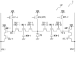
- FIG. 2 is a circuit diagram illustrating a configuration example of a pixel according to the first embodiment of the present disclosure.
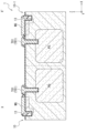
- FIG. 3A is a plan view illustrating a configuration example of a pixel according to the first embodiment of the present disclosure.
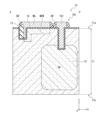
- FIG. 3B is a cross-sectional view showing an example of the configuration of a pixel according to the first embodiment of the present disclosure.
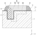
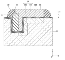
- FIG. 3C is an enlarged cross-sectional view showing the control electrode and its surrounding area shown in FIG. 3B.
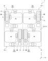
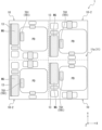
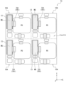
- FIG. 4A is a plan view showing a first example of a pixel arrangement in the imaging device according to the first embodiment of the present disclosure.
- FIG. 4A is a plan view showing a first example of a pixel arrangement in the imaging device according to the first embodiment of the present disclosure.
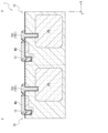
- FIG. 4B is a cross-sectional view taken along line XX' of the plan view shown in FIG. 4A.
- FIG. 5A is a plan view showing a second example of a pixel arrangement in the imaging device according to the first embodiment of the present disclosure.
- FIG. 5B is a cross-sectional view taken along line XX' of the plan view shown in FIG. 5A.
- FIG. 6 is a plan view showing a third example of pixel arrangement in the imaging device according to the first embodiment of the present disclosure.
- FIG. 7 is a plan view showing a fourth example of a pixel arrangement in the imaging device according to the first embodiment of the present disclosure.
- FIG. 8 is a cross-sectional view showing a control electrode and its surrounding area according to a first modification of the first embodiment of the present disclosure.
- FIG. 9 is a cross-sectional view showing a control electrode and its surrounding area according to Modification 2 of the first embodiment of the present disclosure.
- FIG. 10A is a plan view illustrating an example of the configuration of a pixel of an imaging device according to a second embodiment of the present disclosure.
- FIG. 10B is a cross-sectional view showing an example of the configuration of a pixel according to the first embodiment of the present disclosure.
- FIG. 11 is a plan view showing a first example of a pixel arrangement in an imaging device according to a second embodiment of the present disclosure.
- FIG. 12 is a plan view showing a second example of a pixel arrangement in an imaging device according to a second embodiment of the present disclosure.
- FIG. 10A is a plan view illustrating an example of the configuration of a pixel of an imaging device according to a second embodiment of the present disclosure.
- FIG. 10B is a cross-sectional view showing an example of the configuration of a pixel according to the first embodiment of the present disclosure.
- FIG. 13 is a plan view showing a third example of pixel arrangement in an imaging device according to the second embodiment of the present disclosure.
- FIG. 14 is a plan view illustrating a fourth example of a pixel arrangement in an imaging device according to a second embodiment of the present disclosure.
- FIG. 15 is a cross-sectional view showing a control electrode and its surrounding area according to Modification 1 of Embodiment 2 of the present disclosure.
- FIG. 16 is a cross-sectional view showing a control electrode and its surrounding area according to Modification 2 of Embodiment 2 of the present disclosure.
- FIG. 17 is a cross-sectional view showing a control electrode and its surrounding area according to the third modification of the second embodiment of the present disclosure.
- FIG. 15 is a cross-sectional view showing a control electrode and its surrounding area according to Modification 1 of Embodiment 2 of the present disclosure.
- FIG. 16 is a cross-sectional view showing a control electrode and its surrounding area according to Modification 2 of Embodiment 2 of the present
- FIG. 18 is a cross-sectional view showing a control electrode and its surrounding area according to the fourth modification of the second embodiment of the present disclosure.
- FIG. 19 is a plan view illustrating a configuration example of a pixel according to Modification 5 of Embodiment 2 of the present disclosure.
- FIG. 20 is a plan view illustrating an example of the configuration of a pixel of an imaging device according to a third embodiment of the present disclosure.
- FIG. 21 is a plan view illustrating a first example of a pixel arrangement in an imaging device according to a third embodiment of the present disclosure.
- FIG. 22 is a plan view showing a second example of a pixel arrangement in an imaging device according to a third embodiment of the present disclosure.
- FIG. 23A is a plan view illustrating an example of the configuration of a pixel of an imaging device according to a fourth embodiment of the present disclosure.
- FIG. 23B is a cross-sectional view showing a configuration example of a pixel according to the fourth embodiment of the present disclosure.
- FIG. 24A is a plan view showing a first example of a pixel arrangement in an imaging device according to a fourth embodiment of the present disclosure.
- FIG. 24B is a cross-sectional view taken along line X2-X2' of the plan view shown in FIG. 24A.
- FIG. 25A is a plan view showing a second example of a pixel arrangement in an imaging device according to a fourth embodiment of the present disclosure.
- FIG. 25B is a cross-sectional view taken along line X2-X2' of the plan view shown in FIG. 25A.
- FIG. 26 is a plan view illustrating a third example of a pixel arrangement in an imaging device according to a fourth embodiment of the present disclosure.
- FIG. 27 is a plan view showing a fourth example of pixel arrangement in an imaging device according to a fourth embodiment of the present disclosure.
- FIG. 28A is a plan view illustrating an example of the configuration of a pixel of an imaging device according to a fifth embodiment of the present disclosure.
- FIG. 28B is a cross-sectional view showing a configuration example of a pixel according to the fifth embodiment of the present disclosure.
- FIG. 29 is a plan view showing a first example of a pixel arrangement in an imaging device according to a fifth embodiment of the present disclosure.
- FIG. 30 is a plan view showing a second example of a pixel arrangement in an imaging device according to the fifth embodiment of the present disclosure.
- FIG. 31 is a plan view showing a third example of pixel arrangement in an imaging device according to the fifth embodiment of the present disclosure.
- FIG. 32 is a plan view showing a fourth example of a pixel arrangement in an imaging device according to the fifth embodiment of the present disclosure.
- FIG. 33A is a plan view showing an example of the configuration of a pixel of an imaging device according to a sixth embodiment of the present disclosure.
- FIG. 33B is a cross-sectional view showing a configuration example of a pixel according to the sixth embodiment of the present disclosure.
- FIG. 33C is a cross-sectional view showing a configuration example of a pixel according to the sixth embodiment of the present disclosure.
- FIG. 34 is a circuit diagram showing a configuration example of an indirect ToF distance measuring device according to a seventh embodiment of the present disclosure.
- FIG. 35A is a plan view showing a configuration example of a pixel according to the seventh embodiment of the present disclosure.
- FIG. 35B is a cross-sectional view taken along line X5-X5' of the plan view shown in FIG. 35A.
- FIG. 36A is a plan view showing a first example of a pixel arrangement in a distance measuring device according to a seventh embodiment of the present disclosure.
- FIG. 36B is a cross-sectional view showing a first example of a pixel arrangement in a distance measuring device according to the seventh embodiment of the present disclosure.
- FIG. 37 is a plan view showing a second example of pixel arrangement in a distance measuring device according to the seventh embodiment of the present disclosure.
- FIG. 38A is a plan view illustrating a configuration example of a pixel according to an eighth embodiment of the present disclosure.
- FIG. 38B is a cross-sectional view showing a configuration example of a pixel according to embodiment 8 of the present disclosure.
- FIG. 39A is a plan view showing a first example of a pixel arrangement in a distance measuring device according to an eighth embodiment of the present disclosure.
- FIG. 39B is a cross-sectional view showing a first example of a pixel arrangement in a distance measuring device according to an eighth embodiment of the present disclosure.
- FIG. 40 is a plan view showing a second example of pixel arrangement in a distance measuring device according to the eighth embodiment of the present disclosure.
- up and down and other directions in the following explanation are merely for the convenience of explanation and do not limit the technical ideas of this disclosure. For example, if an object is rotated 90 degrees and observed, up and down are converted into left and right and read, and of course, if it is rotated 180 degrees and observed, up and down are read inverted.
- directions may be described using the terms X-axis, Y-axis, and Z-axis.
- the X-axis and Y-axis directions are parallel to the surface 11a of the semiconductor substrate 11 described below.
- the Z-axis direction is the thickness direction of the semiconductor substrate 11 and is the normal direction of the surface 11a of the semiconductor substrate 11.
- the X-axis, Y-axis, and Z-axis directions are mutually perpendicular.
- planar view means, for example, viewing from the thickness direction (e.g., the Z-axis direction) of the semiconductor substrate 11 described below.
- the photodiode PD receives light that is irradiated onto the pixel 10, and generates and accumulates an electric charge according to the amount of light.
- the first transfer transistor TR1 is driven according to a transfer signal supplied from the vertical drive unit 33.
- the first transfer transistor TR1 is turned on, the charge stored in the photodiode PD is transferred to the charge storage unit MEM.
- the second transfer transistor TR2 is driven according to a transfer signal supplied from the vertical drive unit 33.
- the second transfer transistor TR2 is turned on, the charge stored in the charge storage unit MEM is transferred to the floating diffusion region FD.
- the charge storage unit MEM temporarily stores the charge transferred from the photodiode PD via the first transfer transistor TR1.
- the charge storage unit MEM is, for example, a MOS capacitor.
- the control electrode MG controls the potential of the charge storage unit MEM according to a transfer signal supplied from the vertical drive unit 33.
- the control electrode MG is, for example, the gate electrode of a MOS capacitor.
- the transfer signal (voltage) supplied to the control electrode MG controls the potential of the charge storage unit MEM, and the capacitance of the charge storage unit MEM.
- the floating diffusion region FD is a floating diffusion region having a predetermined capacitance formed at the connection point between the second transfer transistor TR2 and the gate electrode of the amplification transistor AMP.
- the floating diffusion region FD accumulates the charge transferred from the charge accumulation unit MEM via the second transfer transistor TR2.
- the amplification transistor AMP is connected to a power supply VDD (not shown) and outputs a pixel signal at a level corresponding to the charge accumulated in the floating diffusion region FD.
- the selection transistor SEL is driven according to a selection signal supplied from the vertical drive unit 33.
- the selection transistor SEL is turned on, the pixel signal output from the amplification transistor AMP can be read out to the vertical signal line 43 via the selection transistor SEL.
- the reset transistor RST is driven according to a reset signal supplied from the vertical drive unit 33.
- the reset transistor RST is turned on, the charge stored in the floating diffusion region FD is discharged to the power supply VDD via the reset transistor RST, and the floating diffusion region FD is reset.
- the discharge transistor OFT is driven according to a discharge signal supplied from the vertical drive unit 33.
- the discharge transistor OFT is turned on, the unnecessary charges stored in the photodiode PD are discharged to the discharge region OFD via the discharge transistor OFT, and the photodiode PD is reset.
- the discharge region OFD is connected to the power supply VDD.
- a high-level discharge signal is supplied to the discharge transistor OFT, turning the discharge transistor OFT on. This causes the charge stored in the photodiode PD to be discharged to the power supply VDD via the discharge region OFD, and the photodiodes PD of all pixels 10 are reset. After the photodiode PD is reset, the discharge transistor OFT is turned off by a low-level discharge signal, and exposure begins in all pixels 10 in the pixel array section 32.
- an imaging device 1 having pixels 10 configured in this way, a global shutter system is adopted, which allows charge to be transferred from the photodiode PD to the charge storage unit MEM simultaneously for all pixels 10, making it possible to make the exposure timing of all pixels 10 the same. This makes it possible to avoid distortion in the image.
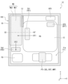
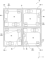
- Fig. 3A is a plan view showing a configuration example of the pixel 10 according to the first embodiment of the present disclosure.
- Fig. 3A is a view of the pixel 10 viewed from above the surface 11a of the semiconductor substrate 11 (an example of the "first surface" of the present disclosure).
- the conductivity type of the semiconductor substrate 11 shown in FIG. 3A is, for example, P type.
- an N-type semiconductor region 12 is formed in the semiconductor substrate 11 in the central region of the pixel 10 and in the region to the right of the central region.
- the N-type semiconductor region 12 constitutes a part of the photodiode PD.
- a discharge region OFD Around the photodiode PD, a discharge region OFD, a control electrode MG, a second transfer transistor TR2, a floating diffusion region FD, and a pixel transistor PTr are arranged.
- the emission region OFD and the floating diffusion region FD are each composed of an N+ type semiconductor region having a higher concentration of N-type impurities than the N-type semiconductor region 12.
- the pixel transistor PTr is at least one of the selection transistor SEL, reset transistor RST, and amplification transistor AMP shown in FIG. 2.
- these three transistors selection transistor SEL, reset transistor RST, and amplification transistor AMP are shown diagrammatically as one pixel transistor PTr.
- the photodiode PD, the discharge region OFD, the control electrode MG, the second transfer transistor TR2, the floating diffusion region FD, and the pixel transistor PTr are each separated from the other elements or regions by a P-type semiconductor substrate 11 (i.e., a P-type region).
- the charge storage unit MEM is disposed at a position overlapping the control electrode MG in the thickness direction of the semiconductor substrate 11 (for example, in the Z-axis direction). In other words, the charge storage unit MEM is disposed below the control electrode MG via an insulating film.
- the gate electrode (hereinafter also referred to as the "first transfer gate”) TG1 of the first transfer transistor TR1 is disposed at a position overlapping with, for example, the outer periphery of the photodiode PD.
- the first transfer transistor TR1 is an N-type MOS transistor.
- the source region of the first transfer transistor TR1 is the N-type semiconductor region 12 of the photodiode PD.
- the drain region of the first transfer transistor TR1 is an N-type semiconductor region that constitutes the charge storage unit MEM.
- the first transfer gate TG1 is disposed at a position adjacent to the P-type semiconductor substrate 11 via a gate insulating film.
- the first transfer transistor TR1 to transfer the charge generated in the photodiode PD to the charge storage unit MEM.
- the first transfer direction DT1 is, for example, the X-axis direction.
- the first transfer direction DT1 is also, for example, the direction in which the first transfer transistor TR1 and the charge storage unit MEM face each other at the shortest distance.
- the gate electrode (hereinafter also referred to as the "second transfer gate") TG2 of the second transfer transistor TR2 is disposed, for example, outside the photodiode PD, between the control electrode MG and the floating diffusion region FD.
- the second transfer transistor TR2 is an N-type MOS transistor.
- the source region of the second transfer transistor TR2 is an N-type semiconductor region that constitutes the charge storage unit MEM.
- the drain region of the second transfer transistor TR2 is an N+ type floating diffusion region FD.
- the second transfer gate TG2 is disposed in a position adjacent to the P-type semiconductor substrate 11 via a gate insulating film.
- the second transfer transistor TR2 to transfer charge from the charge storage unit MEM to the photodiode PD.
- the second transfer direction DT2 is, for example, the Y-axis direction.
- the second transfer direction DT2 is also, for example, the direction in which the charge storage unit MEM and the second transfer transistor TR2 face each other at the shortest distance.
- the gate electrode (hereinafter also referred to as "discharge gate”) OFG of the discharge transistor OFT is arranged at a position overlapping with, for example, the outer periphery of the photodiode PD.
- the discharge transistor OFT is an N-type MOS transistor.
- the source region of the discharge transistor OFT is the N-type semiconductor region 12 of the photodiode PD.
- the drain region of the discharge transistor OFT is an N+ type discharge region OFD.
- the discharge gate OFG is arranged at a position adjacent to the P-type semiconductor substrate 11 via a gate insulating film. This arrangement enables the discharge transistor OFT to discharge the charge generated in the photodiode PD to the discharge region OFD.
- a buried insulating film 13 is provided on the outer periphery of the pixel 10.
- the buried insulating film 13 is disposed on the opposite side of the first transfer gate TG1 with the control electrode MG in between.
- the buried insulating film 13 is, for example, a silicon oxide film or a silicon nitride film, or a film in which a silicon oxide film and a silicon nitride film are stacked.
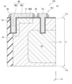
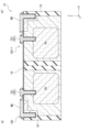
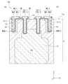
- FIG. 3B is a cross-sectional view showing an example of the configuration of a pixel 10 according to embodiment 1 of the present disclosure.
- FIG. 3B is a cross-sectional view taken along line X-X' in the plan view shown in FIG. 3A.
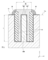
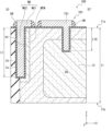
- FIG. 3C is a cross-sectional view showing an enlarged view of the control electrode MG and its surrounding area shown in FIG. 3B.
- a trench H1 is provided in the semiconductor substrate 11 in the depth direction from the front surface 11a (the direction from the front surface 11a to the back surface 11b, for example, the Z-axis direction).
- a buried insulating film 13 is disposed in the trench H1.
- the control electrode MG has a first electrode portion MG1 and a second electrode portion MG2 connected to the first electrode portion MG1.
- the first electrode portion MG1 is provided on the surface 11a of the semiconductor substrate 11.
- the second electrode portion MG2 is embedded from the surface 11a of the semiconductor substrate 11 in the depth direction of the semiconductor substrate 11 (e.g., the Z-axis direction).
- the second electrode portion MG2 is disposed in a trench H1.
- the first electrode portion MG1 is provided parallel to the surface 11a of the semiconductor substrate 11, and therefore may be called a planar portion.
- the second electrode portion MG2 is provided in a direction intersecting the surface 11a of the semiconductor substrate 11 (e.g., a vertical direction), and therefore may be called a vertical portion.
- An insulating film 14 is provided between the control electrode MG and the semiconductor substrate 11.
- the second electrode portion MG2 is disposed in the trench H1 via the insulating film 14.
- the second electrode portion MG2 has a surface adjacent to the charge storage portion MEM via the insulating film 14 (the right surface in Figures 3B and 3C), and an opposite surface (the left surface in Figures 3B and 3C).
- the right surface of the second electrode portion MG2 faces the center of the pixel 10.
- the left surface of the second electrode portion MG2 faces the outer periphery of the pixel 10.
- the embedded insulating film 13 is disposed between the left surface of the second electrode portion MG2 and the side surface of the trench H1.
- the embedded insulating film 13 is disposed within the trench H1, and is located on the opposite side of the charge storage portion MEM across the second electrode portion MG2.
- the second electrode portion MG2 is provided only in the portion adjacent to the buried insulating film 13. In the portion of the control electrode MG that is not adjacent to the buried insulating film 13, the second electrode portion MG2 is not provided, and only the first electrode portion MG1 is provided.
- the buried insulating film 13 has an end 131 that protrudes upward from the opening end of the trench H1.
- the outer periphery of the first electrode portion MG1 is located on this end 131. This makes it possible to increase the distance between the outer periphery of the first electrode portion MG1 and the surface 11a of the semiconductor substrate 11, thereby preventing the electric field from concentrating on the outer periphery of the first electrode portion MG1.
- the charge storage unit MEM is composed of an N-type semiconductor region.
- the charge storage unit MEM is adjacent to the control electrode MG via the insulating film 14.
- the charge storage unit MEM is provided in a region adjacent to the first electrode portion MG1 via the insulating film.
- the charge storage unit MEM is also provided in a region adjacent to the second electrode portion MG2 via the insulating film 14.
- the charge storage unit MEM is provided continuously from the surface 11a of the semiconductor substrate 11 to the bottom of the trench H1 along the first electrode portion MG1 and the second electrode portion MG2. In other words, the charge storage unit MEM is provided continuously from the surface 11a of the semiconductor substrate 11, through the side surface of the trench H1 to the bottom of the trench H1.
- a sidewall SW made of an insulating film may be provided on each side of the first transfer gate TG1 and the control electrode MG.
- a sidewall made of an insulating film may also be provided on the side of the second transfer gate TG2.
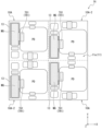
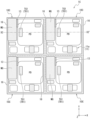
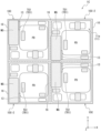
- FIG. 4A is a plan view showing a first example of pixel arrangement in an imaging device 1 according to embodiment 1 of the present disclosure.
- FIG. 4B is a cross-sectional view taken along line X-X' of the plan view shown in FIG. 4A.
- the imaging device 1 has a plurality of pixels 10 arranged in a direction parallel to the surface 11a of the semiconductor substrate 11 (e.g., arranged in a line in the X-axis direction and in the Y-axis direction, respectively).
- the plurality of pixels 10 are arranged adjacent to one another.
- FIG. 5A is a plan view showing pixel arrangement example 2 in the imaging device 1 according to embodiment 1 of the present disclosure.
- FIG. 5B is a cross-sectional view taken along line X-X' of the plan view shown in FIG. 5A.
- the imaging device 1 may have a plurality of pixels 10, 10-1 arranged side by side in the X-axis direction and the Y-axis direction, respectively.
- the pixel 10 is an example of a "first pixel" of the present disclosure
- the pixel 10-1 is an example of a "second pixel" of the present disclosure.
- FIG. 6 is a plan view showing pixel arrangement example 3 in the imaging device 1 according to embodiment 1 of the present disclosure.
- the imaging device 1 may have a plurality of pixels 10, 10-2 arranged side by side in the X-axis direction and the Y-axis direction, respectively.
- the pixel 10 is an example of a "first pixel” in the present disclosure
- the pixel 10-2 is an example of a "second pixel” in the present disclosure.
- the shape of the pixel 10-2 is a shape obtained by inverting the pixel 10 up and down (i.e., a shape obtained by inverting the pixel 10 left and right and rotating it by 180 degrees).
- the pixels 10, 10-2 are arranged alternately and adjacently in the X-axis direction and the Y-axis direction, respectively.
- FIG. 7 is a plan view showing pixel arrangement example 4 in the imaging device 1 according to embodiment 1 of the present disclosure.
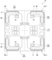
- the imaging device 1 may have a plurality of pixels 10, 10-1, 10-2, and 10-3 arranged side by side in the X-axis direction and the Y-axis direction, respectively.
- Pixel 10 is an example of a "first pixel” in the present disclosure.
- Pixels 10-1, 10-2, and 10-3 are each an example of a "second pixel" in the present disclosure.
- pixel 10-3 In a plan view from the Z-axis direction, pixel 10-3 has a shape obtained by rotating pixel 10 by 180 degrees.
- the pixels 10, 10-1, 10-2, and 10-3 may be arranged alternately in any order in the X-axis direction and the Y-axis direction.
- the pixels 10, 10-1, 10-2, and 10-3 may also be arranged adjacent to one another in any combination.
- the pixels 10, 10-1, 10-2, and 10-3 shown in FIG. 7 may be a set of units, and this unit may be arranged repeatedly in the X-axis direction and the Y-axis direction. These units may also be arranged adjacent to one another.
- the pixels 10 may be inverted in a planar view, rotated, or inverted and rotated. Furthermore, these pixels 10 may be arranged side by side in any combination. This allows for greater freedom in the layout of the pixels 10 in the imaging device 1.
- the imaging device 1 includes a photodiode PD provided in the semiconductor substrate 11 and converting light into an electric charge, a floating diffusion region FD provided in the semiconductor substrate 11 and to which the electric charge generated in the photodiode PD is transferred, a charge accumulation unit MEM provided in the semiconductor substrate 11 and arranged midway along a transfer path along which electric charge is transferred from the photodiode PD to the floating diffusion region FD, a first transfer transistor TR1 arranged on the charge transfer path between the photodiode PD and the charge accumulation unit MEM and transferring electric charge from the photodiode PD to the charge accumulation unit MEM, and a control electrode MG arranged adjacent to the charge accumulation unit MEM and controlling the potential of the charge accumulation unit MEM.
- the control electrode MG has a first electrode portion MG1 provided on the surface 11a of the semiconductor substrate 11 and arranged at a position overlapping the charge storage portion MEM in the thickness direction of the semiconductor substrate 11, and a second electrode portion MG2 connected to the first electrode portion MG1 and embedded from the surface 11a of the semiconductor substrate 11 in the depth direction of the semiconductor substrate 11.
- the second electrode unit MG2 is arranged on the opposite side of the first transfer transistor TR1 across the charge storage unit MEM in the first transfer direction DT1.
- the second electrode unit MG2 is arranged only on the opposite side of the first transfer transistor TR1 across the charge storage unit MEM in the first transfer direction DT1.
- the first electrode portion MG1 is disposed on the surface 11a of the semiconductor substrate 11, and is not disposed inside the semiconductor substrate 11.
- the second electrode portion MG2 is disposed inside the semiconductor substrate 11, but its position is the end position in the first transfer direction DT1 of the charge storage portion MEM, and is not a charge transfer path. Since the control electrode MG is disposed so as not to impede the charge transfer, it is possible to simplify the charge transfer path and improve the charge transfer characteristics (e.g., transfer efficiency).
- the position where the charge storage unit MEM hits the first transfer direction DT1 is a position where charge moving in the first transfer direction DT1 tends to collect. Because the second electrode unit MG2 is disposed at this position, charge can be easily stored in the charge storage unit MEM, and the capacity of the charge storage unit MEM can be efficiently increased.
- the imaging device 1 can achieve both an increase in the capacity of the charge storage unit MEM and improved charge transfer characteristics.
- the second electrode unit MG2 is not disposed between the first transfer transistor TR1 and the charge storage unit MEM in the first transfer direction DT1. This makes it possible for the second electrode unit MG2 not to impede the transfer of charges from the first transfer transistor TR1 to the charge storage unit MEM.
- the second electrode unit MG2 is not disposed between the charge storage unit MEM and the second transfer transistor TR2 in the second transfer direction DT2. This makes it possible for the second electrode unit MG2 not to impede the transfer of charge from the first transfer transistor TR1 to the charge storage unit MEM.
- the imaging device 1 also has a trench H1 provided in the depth direction from the surface 11a of the semiconductor substrate 11, and a buried insulating film 13 provided in the trench H1.
- the second electrode portion MG2 and the buried insulating film 13 are disposed in the trench H1.
- the buried insulating film 13 is located on the opposite side of the charge storage portion MEM across the second electrode portion MG2. This makes it possible for the buried insulating film 13 to prevent the formation of unnecessary electric fields, unnecessary charge storage regions, and unintended channels on the opposite side of the charge storage portion MEM across the second electrode portion MG2 (i.e., outside the second electrode portion MG2). This makes it possible to suppress the generation of noise such as dark current.
- the insulating film 14 disposed between the control electrode MG and the charge storage unit MEM may have a thickness that varies partially.
- Modification 1 8 is a cross-sectional view showing the control electrode MG and its surrounding area according to Modification 1 of the first embodiment of the present disclosure.
- the insulating film 14 disposed between the control electrode MG and the semiconductor substrate 11 may have a first insulating film 141 and a second insulating film 142.
- the first insulating film 141 is provided between the first electrode portion MG1 and the charge storage portion MEM.
- the second insulating film 142 is provided between the second electrode portion MG2 and the charge storage portion MEM.
- the first insulating film 141 and the second insulating film 142 have the same composition.
- the first insulating film 141 and the second insulating film 142 are each composed of a silicon oxide film.
- the first insulating film 141 and the second insulating film 142 have different film thicknesses.
- the film thickness of the first insulating film 141 is thinner than the film thickness of the second insulating film 142.
- the electric field is likely to concentrate at the corner of the second electrode portion MG2 located at the bottom of the trench H1, but by providing a thick second insulating film 142 in the area including this corner, the electric field concentration can be suppressed. This makes it possible to suppress the generation of noise such as dark current caused by the electric field concentration.
- the electric field is less likely to concentrate on the surface 11a of the semiconductor substrate 11 than on the above-mentioned corners.
- a thin first insulating film 141 on the surface 11a where the electric field is less likely to concentrate, it becomes possible to accumulate more charge in the charge storage unit MEM below the first insulating film 141. It is possible to further increase the capacity of the charge storage unit MEM while suppressing the generation of noise such as dark current.
- Modification 2 9 is a cross-sectional view showing the control electrode MG and its surrounding area according to the second modification of the first embodiment of the present disclosure.
- the insulating film 14 disposed between the control electrode MG and the semiconductor substrate 11 may have a first insulating film 141, a third insulating film 143, and a fourth insulating film 144.
- the first insulating film 141 is provided between the first electrode portion MG1 and the charge storage portion MEM, and between the second electrode portion MG2 and the charge storage portion MEM.
- the third insulating film 143 is provided between the corner of the region where the first electrode portion MG1 and the second electrode portion MG2 are connected (i.e., the corner of the opening end of the trench H1) and the charge storage portion MEM.
- the fourth insulating film 144 is provided from the bottom of the trench H1 through between the side surface of the trench H1 and the embedded insulating film 13 to the surface 11a of the semiconductor substrate 11.
- the first insulating film 141, the third insulating film 143, and the fourth insulating film 144 have the same composition.
- the first insulating film 141, the third insulating film 143, and the fourth insulating film 144 are each composed of a silicon oxide film.
- the first insulating film 141 and the third insulating film 143 have different thicknesses.
- the third insulating film 143 is thicker than the first insulating film 141.
- the thick third insulating film 143 can suppress electric field concentration at the corners of the opening end of the trench H1, and can suppress the generation of noise such as dark current.
- the thin first insulating film 141 can further increase the capacity of the charge storage unit MEM.
- the first insulating film 141 and the fourth insulating film 144 have different thicknesses.
- the fourth insulating film 144 is thicker than the first insulating film 141.
- the thick fourth insulating film 144 can suppress electric field concentration at the corners of the bottom of the trench H1, and can suppress the generation of noise such as dark current.
- the second electrode unit MG2 is described as being disposed only on the opposite side of the first transfer transistor TR1 across the charge storage unit MEM in the first transfer direction DT1.
- the arrangement of the second electrode unit MG2 is not limited to this.
- the second electrode unit MG2 may be disposed in other regions in addition to the opposite side of the first transfer transistor TR1.
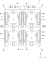
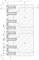
- FIG. 10A is a plan view showing an example of the configuration of a pixel 10A of an imaging device 1A according to embodiment 2 of the present disclosure.
- FIG. 10B is a cross-sectional view showing an example of the configuration of a pixel 10A according to embodiment 1 of the present disclosure.
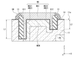
- FIG. 10B is a cross-sectional view obtained by cutting the plan view shown in FIG. 10A along line X1-X1'. Note that line X-X' and line X1-X1' are also shown in the plan view shown in FIG. 10A.
- the cross-sectional view obtained by cutting the plan view shown in FIG. 10A along line X-X' and its enlarged view are the same as those shown in FIGS. 3B and 3C, and therefore will not be shown.
- the pixel 10A shown in Figures 10A and 10B differs from the pixel 10 shown in Figures 3A to 3C in the arrangement of the trench H1, the second electrode portion MG2, and the embedded insulating film 13. The rest of the configuration is the same, so a description thereof will be omitted.
- the trench H1, the second electrode portion MG2, and the embedded insulating film 13 are arranged along the entire periphery of the charge storage portion MEM, except between the first transfer transistor TR1 and the charge storage portion MEM in the first transfer direction DT1, and between the charge storage portion MEM and the second transfer transistor TR2 in the second transfer direction DT2.
- a trench H1 is provided on both sides of the charge storage unit MEM.
- a second electrode unit MG2 and a buried insulating film 13 are disposed within the trench H1.
- the buried insulating film 13 is disposed on the opposite side of the charge storage unit MEM, sandwiching the second electrode unit MG2 therebetween.
- multiple pixels 10A can be arranged side by side.
- FIG. 11 is a plan view showing pixel arrangement example 1 in an imaging device 1A according to embodiment 2 of the present disclosure (an example of the "photodetection device" of the present disclosure).
- the imaging device 1A has a plurality of pixels 10A arranged in a direction parallel to the surface 11a of the semiconductor substrate 11 (e.g., arranged in a line in the X-axis direction and in the Y-axis direction, respectively).
- the plurality of pixels 10A are arranged adjacent to one another.
- FIG. 12 is a plan view showing pixel arrangement example 2 in an imaging device 1A according to embodiment 2 of the present disclosure.
- imaging device 1A may have a plurality of pixels 10A, 10A-1 arranged side by side in the X-axis direction and in the Y-axis direction, respectively.
- Pixel 10A is an example of a "first pixel” in the present disclosure
- pixel 10A-1 is an example of a "second pixel” in the present disclosure.
- pixel 10A-1 When viewed from a plan view in the Z-axis direction, pixel 10A-1 has a shape obtained by left-right inverting pixel 10A. Pixels 10A, 10A-1 are arranged alternately and adjacently in the X-axis direction and in the Y-axis direction, respectively.
- FIG. 13 is a plan view showing pixel arrangement example 3 in an imaging device 1A according to embodiment 2 of the present disclosure.
- imaging device 1A may have a plurality of pixels 10A, 10A-2 arranged side by side in the X-axis direction and in the Y-axis direction, respectively.
- Pixel 10A is an example of a "first pixel” in the present disclosure
- pixel 10A-2 is an example of a "second pixel” in the present disclosure.
- pixel 10A-2 In a plan view from the Z-axis direction, pixel 10A-2 has a shape obtained by inverting pixel 10A upside down. Pixels 10A, 10A-2 are arranged alternately and adjacently in the X-axis direction and in the Y-axis direction, respectively.
- FIG. 14 is a plan view showing pixel arrangement example 4 in an imaging device 1A according to embodiment 2 of the present disclosure.
- imaging device 1A may have a plurality of pixels 10A, 10A-1, 10A-2, and 10A-3 arranged side by side in the X-axis direction and the Y-axis direction, respectively.
- Pixel 10A is an example of a "first pixel” in the present disclosure.
- Pixels 10A-1, 10A-2, and 10A-3 are each an example of a "second pixel" in the present disclosure.
- pixel 10A-3 When viewed from above in the Z-axis direction, pixel 10A-3 has a shape that is the same as pixel 10A rotated 180 degrees.
- the pixels 10A, 10A-1, 10A-2, and 10A-3 may be arranged alternately in any order in the X-axis direction and the Y-axis direction.
- the pixels 10A, 10A-1, 10A-2, and 10A-3 may also be arranged adjacent to one another in any combination.
- the pixels 10A, 10A-1, 10A-2, and 10A-3 shown in FIG. 14 may be a set of units, and this unit may be arranged repeatedly in the X-axis direction and the Y-axis direction. These units may also be arranged adjacent to one another.
- the pixels 10A may be inverted in a planar view, rotated, or inverted and rotated. Furthermore, these pixels 10A may be arranged side by side in any combination. This increases the degree of freedom in the layout of the pixels 10A in the imaging device 1A.
- the control electrode MG is arranged so as not to impede the transfer of charges, and the charge transfer path is simplified.
- the second electrode portion MG2 of the control electrode MG is arranged at the end of the charge storage unit MEM in the first transfer direction DT1, it is possible to efficiently increase the capacity of the charge storage unit MEM. This makes it possible to achieve both an increase in the capacity of the charge storage unit MEM and improved charge transfer characteristics.
- the second electrode portion MG2 of the control electrode MG is disposed along the entire periphery of the charge storage portion MEM, except for between the first transfer transistor TR1 and the charge storage portion MEM in the first transfer direction DT1, and between the charge storage portion MEM and the second transfer transistor TR2 in the second transfer direction DT2. This increases the opposing area between the second electrode portion MG2 and the charge storage portion MEM, making it possible to further increase the capacity of the charge storage portion MEM.
- Modification of the second embodiment (1) Modification 1 Fig. 15 is a cross-sectional view showing the control electrode MG and its surrounding area according to Modification 1 of the embodiment 2 of the present disclosure.
- the cross-sectional view shown in Fig. 15 is different from the cross-sectional view shown in Fig. 10B in that the depth from the surface 11a of the trench H1 is deeper and the length of the second electrode portion MG2 in the depth direction (e.g., the Z-axis direction) is longer.
- the charge storage portion MEM is sandwiched on both sides by the second electrode portion MG2.
- the length of the first electrode portion MG1 in the width direction e.g., the X-axis direction
- the length of the second electrode portion MG2 in the depth direction (e.g., the Z-axis direction) from the surface 11a is L
- W ⁇ L the second electrode portion MG2, which is a recessed portion
- Modification 2 16 is a cross-sectional view showing the control electrode MG and its surrounding area according to the second modification of the second embodiment of the present disclosure.
- the second electrode portion MG2 has a third electrode portion MG21 located on one side of the control electrode MG and a fourth electrode portion MG22 located on one side of the control electrode MG.
- the third electrode portion MG21 is located on the side closer to the outer periphery of the pixel
- the fourth electrode portion MG22 is located on the side closer to the center of the pixel.
- the length L1 of the third electrode portion MG21 in the depth direction (e.g., Z-axis direction) from the surface 11a is different from the length L2 of the third electrode portion MG21 in the depth direction (e.g., Z-axis direction) from the surface 11a.
- the photodiode PD can be extended up to the vicinity directly below the third electrode portion MG21.
- the fourth electrode portion MG22 is positioned so as to overlap the photodiode PD
- the third electrode portion MG21 is positioned so as not to overlap the photodiode PD. This makes it possible to increase the area of the photodiode PD, and therefore the saturation charge amount (Qs).
- FIG. 17 is a cross-sectional view showing the control electrode MG and its surrounding area according to the third modification of the second embodiment of the present disclosure.
- the first insulating film 141 and the second insulating film 142 have the same composition.
- the first insulating film 141 and the second insulating film 142 are each composed of a silicon oxide film.
- the first insulating film 141 and the second insulating film 142 have different film thicknesses.
- the film thickness of the first insulating film 141 is thinner than the film thickness of the second insulating film 142. This makes it possible to further increase the capacity of the charge storage unit MEM while suppressing electric field concentration at the corners and suppressing noise generation such as dark current.
- Fig. 18 is a cross-sectional view showing a control electrode MG and its surrounding area according to a fourth modification of the second embodiment of the present disclosure.
- the first insulating film 141, the third insulating film 143, and the fourth insulating film 144 have the same composition.
- the first insulating film 141, the third insulating film 143, and the fourth insulating film 144 are each composed of a silicon oxide film.
- the first insulating film 141 and the third insulating film 143 have different thicknesses.
- the third insulating film 143 disposed near the corner of the opening end of the trench H1 is thicker than the first insulating film 141.
- the first insulating film 141 and the fourth insulating film 144 have different thicknesses.
- the fourth insulating film 144 disposed between the side surface of the trench H1 and the buried insulating film 13 is thicker than the first insulating film 141. This makes it possible to further increase the capacity of the charge storage unit MEM while suppressing electric field concentration at the corners and suppressing noise generation such as dark current.
- Modification 5 19 is a plan view showing a configuration example of a pixel 10AA according to Modification 5 of the second embodiment of the present disclosure.
- the pixel 10AA shown in FIG. 19 is different from the pixel 10A shown in FIG. 10A in that at least one of the multiple corners MG-C of the control electrode MG is chamfered to be composed of multiple obtuse angles or curves when viewed in a plan view from the Z-axis direction.
- three corners out of the four corners MG-C of the control electrode MG are chamfered.
- Each of the three corners is chamfered to be composed of two obtuse angles (for example, an interior angle of 135° C.).
- multiple pixels 10AA may be arranged side by side in the X-axis direction and the Y-axis direction.
- the shape of at least some of the multiple pixels 10AA in a plan view may be an inverted shape of pixel 10AA, a rotated shape of pixel 10AA, or a shape of pixel 10AA that is inverted and then rotated.
- these pixels 10AA may be arranged side by side in any combination. This increases the degree of freedom in the layout of pixels 10F in the imaging device 1A.
- This modification 5 has the same effect as the above embodiment 2.
- the corner MG-C of the control electrode MG is chamfered, it is possible to suppress electric field concentration at the corner MG-C. This makes it possible to further suppress the generation of noise such as dark current.
- the shape of the control electrode MG is rectangular or rectangular with chamfered corners MG-C in plan view from the Z-axis direction.
- the shape of the control electrode MG in plan view is not limited to rectangular.
- the shape of the control electrode MG in plan view may be L-shaped. At least a part of the corner of the L-shape may be chamfered.
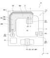
- FIG. 20 is a plan view showing an example configuration of pixel 10B of imaging device 1B according to embodiment 3 of the present disclosure.
- the pixel 10B shown in FIG. 20 differs from pixel 10 shown in FIGS. 3A to 3C in that the control electrode MG has an L-shape when viewed in a plan view from the Z-axis direction. Also, a buried insulating film 13 is provided along the outer periphery of this L-shape. The rest of the configuration is the same, so a description thereof will be omitted. Note that the cross-sectional view taken along line Y-Y' of the plan view shown in FIG. 20 and its enlarged view are the same as those in FIGS. 3B and 3C.
- the control electrode MG of pixel 10B has an L-shape in plan view.
- the control electrode MG has a first portion MGA extending in the X-axis direction and a second portion MGB extending in the Y-axis direction.
- One end of the first portion MGA in the X-axis direction is connected to one end of the second portion MGB in the Y-axis direction, forming the L-shape.
- the second electrode portion MG2 is provided along the outer periphery of the control electrode MG.
- the second electrode portion MG2 is disposed at least on the opposite side of the first transfer transistor TR1 in the first transfer direction DT1, with the charge storage portion MEM in between.
- the embedded insulating film 13 is also provided along the outer periphery of the control electrode MG.
- control electrode MG Since the control electrode MG has an L-shape in a planar view, the charge storage unit MEM located below it is also L-shaped, and the charge transfer path is also L-shaped. Compared to when the control electrode MG has a linear shape in a planar view, it is easier to increase the length of the control electrode MG within pixel 10B. It is easier to increase the capacitance of the charge storage unit MEM located below the control electrode MG.
- At least a portion of the corner MG-C of the control electrode MG is chamfered in plan view.
- the corner MG-C of the connection between the first portion MGA extending in the X-axis direction and the second portion MGB extending in the Y-axis direction is chamfered. This makes it possible to suppress electric field concentration at the corner MG-C, and further suppress the generation of noise such as dark current.
- a plurality of pixels 10B can be arranged side by side. At least some of the plurality of pixels 10B may have a shape obtained by inverting the pixels 10B, rotating the pixels 10B, or inverting and then rotating the pixels 10B. Arrangement examples 1 and 2 are shown below.
- FIG. 21 is a plan view showing pixel arrangement example 1 in an imaging device 1B (an example of a "photodetector" of the present disclosure) according to embodiment 3 of the present disclosure.
- the imaging device 1B has a plurality of pixels 10B arranged in a direction parallel to the surface 11a of the semiconductor substrate 11 (e.g., arranged in a line in the X-axis direction and in the Y-axis direction, respectively).
- the plurality of pixels 10B are arranged adjacent to one another.
- FIG. 22 is a plan view showing pixel arrangement example 2 in an imaging device 1B according to embodiment 3 of the present disclosure.
- imaging device 1B may have a plurality of pixels 10B, 10B-1, 10B-2, and 10B-3 arranged side by side in the X-axis direction and the Y-axis direction, respectively.
- Pixel 10B is an example of a "first pixel” in the present disclosure.
- Pixels 10B-1, 10B-2, and 10B-3 are each an example of a "second pixel" in the present disclosure.
- pixel 10B-1 When viewed from above in the Z-axis direction, pixel 10B-1 has a shape that is the same as pixel 10B when flipped left to right. Pixel 10B-2 has a shape that is the same as pixel 10B when flipped upside down. Pixel 10B-3 has a shape that is the same as pixel 10B when rotated 180 degrees.
- the pixels 10B, 10B-1, 10B-2, and 10B-3 may be alternately arranged in any order in the X-axis direction and the Y-axis direction.
- the pixels 10B, 10B-1, 10B-2, and 10B-3 may be arranged adjacent to one another in any combination.
- the pixels 10B, 10B-1, 10B-2, and 10B-3 shown in FIG. 22 may be a set of units, and this unit may be repeatedly arranged in the X-axis direction and the Y-axis direction. These units may be arranged adjacent to one another.
- the pixels 10B may be inverted in a planar view, rotated, or inverted and rotated. Furthermore, these pixels 10B may be arranged side by side in any combination. This increases the degree of freedom in the layout of the pixels 10B in the imaging device 1B.
- the control electrode MG is arranged so as not to impede the transfer of charges, and the charge transfer path is simplified.
- the second electrode portion MG2 of the control electrode MG is arranged at the end of the charge storage unit MEM in the first transfer direction DT1, it is possible to efficiently increase the capacity of the charge storage unit MEM. This makes it possible to achieve both an increase in the capacity of the charge storage unit MEM and improved charge transfer characteristics.
- control electrode MG has an L-shape in a plan view, it is easy to increase the length of the control electrode MG in the charge transfer direction (i.e., the length of the charge storage unit MEM). This allows more charge to be stored in the charge storage unit MEM, making it possible to increase the signal output of the pixel.
- the second electrode portion MG2 is provided along the outer periphery of the control electrode MG.
- the third embodiment of the present disclosure is not limited to this.
- the second portion MGB extending in the Y-axis direction may be composed of only the first electrode portion MG1.
- the second electrode portion MG2 may be arranged only on the outer periphery of the first portion MGA extending in the X-axis direction.
- the second electrode portion MG2 may be arranged only in a region of the outer periphery of the first portion MGA that is located on the opposite side of the first transfer transistor TR1 across the charge storage portion MEM in the first transfer direction DT1.
- an inter-pixel isolation portion may be disposed between adjacent pixels.
- the inter-pixel isolation portion may be a penetrating isolation portion that penetrates the semiconductor substrate 11, or a non-penetrating isolation portion that is provided from the front surface 11a side (or the back surface 11b side) of the semiconductor substrate 11 to a midway position in the thickness direction of the semiconductor substrate 11.
- at least a part of the embedded insulating film 13 that is disposed along the second electrode portion MG2 may also serve as the inter-pixel isolation portion.
- FIG. 23A is a plan view showing an example of the configuration of a pixel 10C of an imaging device 1C (an example of a "photodetector" of the present disclosure) according to embodiment 4 of the present disclosure.
- FIG. 23B is a cross-sectional view showing an example of the configuration of a pixel 10C according to embodiment 4 of the present disclosure.
- FIG. 23B is a cross-sectional view taken along line X2-X2' of the plan view shown in FIG. 23A.
- the pixel 10C shown in Figures 23A and 23B differs from the pixel 10 shown in Figures 3A to 3C in that an inter-pixel isolation section 16 is disposed on the outer periphery of the pixel 10C, and that a portion of the embedded insulating film 13 disposed along the second electrode section MG2 doubles as the inter-pixel isolation section 16. Other than that, the configuration is the same, so a description thereof will be omitted.
- the imaging device 1C has an inter-pixel isolation section 16.
- the inter-pixel isolation section 16 is composed of an insulating film such as a silicon oxide film or a silicon nitride film.
- the inter-pixel isolation section 16 is disposed on the outer periphery of the pixel 10C, and electrically isolates one pixel 10C from the other adjacent pixel 10C.
- the inter-pixel isolation portion 16 also serves as part of the embedded insulating film 13 arranged along the second electrode portion MG2. In other words, part of the embedded insulating film 13 is replaced with the inter-pixel isolation portion 16.
- Each of the multiple pixels 10C has a photodiode PD, a first transfer transistor TR1, a charge storage unit MEM, a control electrode MG, a second transfer transistor TR2, a floating diffusion region FD, a reset transistor RST, an amplification transistor AMP, and a selection transistor SEL.
- a photodiode PD a photodiode PD
- a first transfer transistor TR1 a charge storage unit MEM
- a control electrode MG a control electrode MG
- a second transfer transistor TR2 a floating diffusion region FD
- a reset transistor RST an amplification transistor AMP
- SEL selection transistor
- FIG. 24A is a plan view showing a first example of pixel arrangement in an imaging device 1C according to embodiment 4 of the present disclosure.
- FIG. 24B is a cross-sectional view taken along line X2-X2' of the plan view shown in FIG. 24A.
- the imaging device 1C has a plurality of pixels 10C arranged side by side in a direction parallel to the surface 11a of the semiconductor substrate 11 (e.g., arranged side by side in the X-axis direction and the Y-axis direction, respectively).
- the plurality of pixels 10C are arranged adjacent to one another.
- FIG. 25A is a plan view showing pixel arrangement example 2 in an imaging device 1C according to embodiment 4 of the present disclosure.
- FIG. 25B is a cross-sectional view of the plan view shown in FIG. 25A cut along line X2-X2'.
- the imaging device 1C may have a plurality of pixels 10C, 10C-1 arranged side by side in the X-axis direction and the Y-axis direction, respectively.
- the pixel 10C is an example of a "first pixel" of the present disclosure
- the pixel 10C-1 is an example of a "second pixel" of the present disclosure.
- the shape of the pixel 10C-1 is a shape obtained by left-right inverting the shape of the pixel 10C.
- the pixels 10C, 10C-1 are arranged alternately and adjacently in the X-axis direction and the Y-axis direction, respectively.
- FIG. 26 is a plan view showing pixel arrangement example 3 in an imaging device 1C according to embodiment 4 of the present disclosure.
- imaging device 1C may have a plurality of pixels 10C, 10C-2 arranged side by side in the X-axis direction and in the Y-axis direction, respectively.
- Pixel 10C is an example of a "first pixel” in the present disclosure
- pixel 10C-2 is an example of a "second pixel” in the present disclosure.
- pixel 10C-2 In a plan view from the Z-axis direction, pixel 10C-2 has a shape obtained by inverting pixel 10C upside down. Pixels 10C, 10C-2 are arranged alternately and adjacently in the X-axis direction and in the Y-axis direction, respectively.
- FIG. 27 is a plan view showing pixel arrangement example 4 in an imaging device 1C according to embodiment 4 of the present disclosure.
- imaging device 1C may have a plurality of pixels 10C, 10C-1, 10C-2, and 10C-3 arranged side by side in the X-axis direction and the Y-axis direction, respectively.
- Pixel 10C is an example of a "first pixel” in the present disclosure.
- Pixels 10C-1, 10C-2, and 10C-3 are each an example of a "second pixel" in the present disclosure.
- pixel 10C-3 In a plan view from the Z-axis direction, pixel 10C-3 has a shape obtained by rotating pixel 10C by 180 degrees.
- the pixels 10C, 10C-1, 10C-2, and 10C-3 may be alternately arranged in any order in the X-axis direction and the Y-axis direction.
- the pixels 10C, 10C-1, 10C-2, and 10C-3 may be arranged adjacent to one another in any combination.
- the pixels 10C, 10C-1, 10C-2, and 10C-3 shown in FIG. 27 may be a set of units, and this unit may be repeatedly arranged in the X-axis direction and the Y-axis direction. These units may be arranged adjacent to one another.
- the pixels 10C may be inverted in a planar view, rotated, or inverted and rotated. Furthermore, these pixels 10C may be arranged side by side in any combination. This allows for greater freedom in the layout of the pixels 10C in the imaging device 1C.
- the control electrode MG is arranged so as not to impede the transfer of charges, and the charge transfer path is simplified. Furthermore, since the second electrode portion MG2 of the control electrode MG is arranged at the end of the charge storage portion MEM in the first transfer direction DT1, it is possible to efficiently increase the capacity of the charge storage portion MEM. This makes it possible to simultaneously increase the capacity of the charge storage portion MEM and improve the charge transfer characteristics. Furthermore, since at least a portion of the embedded insulating film 13 is also used as the inter-pixel separation portion 16, it is possible to reduce the area of the embedded insulating film 13 by the amount of the portion used for the same. This makes it possible to further miniaturize and reduce the area of the pixel 10C.
- FIG. 28A is a plan view showing an example of the configuration of a pixel 10D of an imaging device 1C according to embodiment 5 of the present disclosure.
- FIG. 28B is a cross-sectional view showing an example of the configuration of a pixel 10D according to embodiment 5 of the present disclosure.
- FIG. 28B is a cross-sectional view taken along line X3-X3' of the plan view shown in FIG. 28A.
- Pixel 10D shown in Figures 28A and 28B differs from pixel 10C shown in Figures 25A and 25B in that the "buried oxide film" of the present disclosure is used in its entirety as inter-pixel isolation portion 16, that the control electrode MG is formed long along inter-pixel isolation portion 16 and the second electrode portion MG2 is formed deep, and that the width of the control electrode MG in a plan view (width in the X-axis direction in Figure 25A) is partially different. Other than that, the configuration is the same, so a description thereof will be omitted.
- pixel 10D does not have the buried insulating film 13 shown in Figures 28A and 28B.
- the second electrode portion MG2 is disposed along the inter-pixel isolation portion 16, which is an example of the "buried oxide film" of the present disclosure. Even with this configuration, by arranging the second electrode portion MG2 so as not to impede the transfer of charges, it is possible to achieve both an increase in the capacity of the charge storage portion MEM and improved charge transfer characteristics. In addition, because the entire buried insulating film 13 is also used as the inter-pixel isolation portion 16, pixel 10C can be further miniaturized and its area reduced.
- the control electrode MG is formed long along the inter-pixel separation portion 16.
- the second electrode portion MG2 of the control electrode MG is formed long in the depth direction (e.g., the Z-axis direction) from the surface 11a of the semiconductor substrate 11. For example, if the length of the second electrode portion MG2 in the depth direction from the surface 11a is L, and the length of the first transfer gate TG1 having a trench gate structure in the depth direction from the surface 11a is LTG, then L is longer than LTG (L>LTG).
- width W1 of the portion of the control electrode MG facing the second transfer transistor TR2 is larger than the width W2 of the other portion (W1>W2). This makes it possible to improve the efficiency of charge transfer from the charge storage unit MEM to the floating diffusion region FD by the second transfer transistor TR2.
- FIG. 29 is a plan view showing pixel arrangement example 1 in an imaging device 1D (an example of a "photodetector" of the present disclosure) according to embodiment 5 of the present disclosure.
- the imaging device 1D has a plurality of pixels 10D arranged in a direction parallel to the surface 11a of the semiconductor substrate 11 (e.g., arranged in a line in the X-axis direction and the Y-axis direction, respectively).
- the plurality of pixels 10D are arranged adjacent to one another.
- FIG. 30 is a plan view showing pixel arrangement example 2 in an imaging device 1D according to embodiment 5 of the present disclosure.
- imaging device 1D may have a plurality of pixels 10D, 10D-1 arranged side by side in the X-axis direction and in the Y-axis direction, respectively.
- Pixel 10D is an example of a "first pixel” in the present disclosure
- pixel 10D-1 is an example of a "second pixel” in the present disclosure.
- pixel 10D-1 In a plan view from the Z-axis direction, pixel 10D-1 has a shape obtained by left-right inverting pixel 10D. Pixels 10D, 10D-1 are arranged alternately and adjacently in the X-axis direction and in the Y-axis direction, respectively.
- FIG. 31 is a plan view showing pixel arrangement example 3 in an imaging device 1D according to embodiment 5 of the present disclosure.
- imaging device 1D may have a plurality of pixels 10D, 10D-2 arranged side by side in the X-axis direction and in the Y-axis direction, respectively.
- Pixel 10D is an example of a "first pixel” in the present disclosure
- pixel 10D-2 is an example of a "second pixel” in the present disclosure.
- pixel 10D-2 In a plan view from the Z-axis direction, pixel 10D-2 has a shape obtained by inverting pixel 10D upside down. Pixels 10D, 10D-2 are arranged alternately and adjacently in the X-axis direction and in the Y-axis direction, respectively.
- FIG. 32 is a plan view showing pixel arrangement example 4 in an imaging device 1D according to embodiment 5 of the present disclosure.
- imaging device 1D may have a plurality of pixels 10D, 10D-1, 10D-2, and 10D-3 arranged side by side in the X-axis direction and the Y-axis direction, respectively.
- Pixel 10D is an example of a "first pixel” in the present disclosure.
- Pixels 10D-1, 10D-2, and 10D-3 are each an example of a "second pixel" in the present disclosure.
- pixel 10D-3 When viewed from above in the Z-axis direction, pixel 10D-3 has a shape that is the same as pixel 10D rotated 180 degrees.
- the pixels 10D, 10D-1, 10D-2, and 10D-3 may be alternately arranged in any order in the X-axis direction and the Y-axis direction.
- the pixels 10D, 10D-1, 10D-2, and 10D-3 may also be arranged adjacent to one another in any combination.
- the pixels 10D, 10D-1, 10D-2, and 10D-3 shown in FIG. 32 may be a set of units, and this unit may be repeatedly arranged in the X-axis direction and the Y-axis direction. These units may also be arranged adjacent to one another.
- the pixels 10D may be inverted in a planar view, rotated, or inverted and rotated. Furthermore, these pixels 10D may be arranged side by side in any combination. This allows for greater freedom in the layout of the pixels 10D in the imaging device 1D.
- the control electrode MG is arranged so as not to impede the transfer of charges, and the charge transfer path is simplified. Furthermore, since the second electrode portion MG2 of the control electrode MG is arranged at the end of the charge storage unit MEM in the first transfer direction DT1, it is possible to efficiently increase the capacity of the charge storage unit MEM. This makes it possible to simultaneously increase the capacity of the charge storage unit MEM and improve the charge transfer characteristics. Furthermore, since the entire embedded insulating film 13 is also used as the inter-pixel separation portion 16, it is possible to further miniaturize the pixel 10C and reduce its area.
- a light-shielding film may be provided between the photodiode PD and the charge accumulation unit MEM.
- FIG. 33A is a plan view showing an example of the configuration of a pixel 10E of an imaging device 1E (an example of a "photodetector" of the present disclosure) according to embodiment 6 of the present disclosure.
- FIGS. 33B and 33C are cross-sectional views showing an example of the configuration of a pixel 10E according to embodiment 6 of the present disclosure.
- FIG. 33B is a cross-sectional view of the plan view shown in FIG. 33A taken along line X4-X4'.
- FIG. 33C is a cross-sectional view of the plan view shown in FIG. 33A taken along line Y4-Y4'.
- inter-pixel separation portion 16 has light-shielding film 17 and insulating film 18 arranged to sandwich light-shielding film 17 from both sides.
- Light-shielding film 17 is made of, for example, copper (Cu), aluminum (Al), or tungsten (W).
- Insulating film 18 is made of, for example, silicon oxide film or silicon nitride film. This allows light to be shielded between adjacent pixels, and prevents color mixing, etc.
- the light-shielding film 17 and the insulating film 18 extend not only to the outer periphery of the pixel 10E but also from the outer periphery of the pixel 10E to the center of the pixel 10E, and are interposed between the photodiode PD and the charge storage unit MEM.
- the light-shielding film 17 separates the photodiode PD from the charge storage unit MEM.
- a plurality of pixels 10E may be arranged side by side in the X-axis direction and the Y-axis direction.
- the shape of at least some of the plurality of pixels 10E in a planar view may be an inverted shape of the pixel 10E, a rotated shape of the pixel 10E, or a shape of the pixel 10E that is inverted and then rotated.
- these pixels 10E may be arranged side by side in any combination. This allows for greater freedom in the layout of the pixels 10E in the imaging device 1E.
- the control electrode MG is arranged so as not to impede the transfer of charges, and the charge transfer path is simplified.
- the second electrode portion MG2 of the control electrode MG is arranged at the end of the charge storage unit MEM in the first transfer direction DT1, it is possible to efficiently increase the capacity of the charge storage unit MEM. This makes it possible to achieve both an increase in the capacity of the charge storage unit MEM and improved charge transfer characteristics.
- a global shutter type imaging device has been described as an example of the photodetection device of the present disclosure.
- the photodetection device of the present disclosure is not limited to a global shutter type imaging device.
- the photodetection device of the present disclosure may be applied to, for example, an indirect ToF type distance measuring device.
- FIG. 34 is a circuit diagram showing a configuration example of an indirect ToF distance measuring device 2 (an example of the "photodetection device" of the present disclosure) according to embodiment 7 of the present disclosure.
- pixel 10F has a photodiode PD as a photoelectric conversion unit that converts light into electric charge, and a discharge transistor OFT.
- pixel 10F has two each of a first transfer transistor TR1, a charge storage unit MEM, a control electrode MG, a second transfer transistor TR2, a floating diffusion region FD, a reset transistor RST, an amplification transistor AMP, and a selection transistor SEL.
- the charge generated in the photodiode PD is distributed by the first transfer transistors TR1-1 and Tr1-2.
- the sources of the first transfer transistors TR1-1 and TR1-2 are electrically connected to the photodiode PD, and the drains of the first transfer transistors TR1-1 and TR1-2 are electrically connected to the charge storage units MEM-1 and MEM-2, respectively.
- the first transfer transistors TR1-1 and TR1-2 become conductive in response to the voltage applied to their gates, and transfer the charge stored in the photodiode PD to the charge storage units MEM-1 and MEM-2, respectively.
- the voltages applied to the gates of the first transfer transistors TR1-1 and TR1-2 are changed at different times to distribute the charge stored in the photodiode PD to one of the two charge storage units MEM-1 and MEM-2.
- the sources of the second transfer transistors TR2-1 and TR2-2 are electrically connected to the charge storage units MEM-1 and MEM-2. Furthermore, the drains of the second transfer transistors TR2-1 and TR2-2 are electrically connected to the floating diffusion regions FD-1 and FD-2. Then, the second transfer transistors TR2-1 and TR2-2 become conductive in response to a voltage applied to their gates, and can transfer the charges stored in the charge storage units MEM-1 and MEM-2 to the floating diffusion regions FD-1 and FD-2. Note that in embodiment 6 of the present disclosure, since there are two charge storage units MEM-1 and MEM-2, it is also possible for the second transfer transistors TR2-1 and TR2-2 to share one floating diffusion region FD.
- the floating diffusion regions FD-1, FD-2 are electrically connected to the gates of the amplification transistors AMP-1, AMP-2, which convert the charge into a voltage and output it as a signal. Furthermore, the sources of the amplification transistors AMP-1, AMP-2 are connected to the drains of the selection transistors SEL-1, SEL-2, which output the signal obtained by conversion to the signal lines VSL1, VSL2 in accordance with a selection signal. Furthermore, the drains of the amplification transistors AMP-1, AMP-2 are electrically connected to the power supply VDD.
- the sources of the selection transistors SEL-1 and SEL-2 are electrically connected to the signal lines VSL1 and VSL2 that transmit the converted voltage as a signal, and are further electrically connected to the above-mentioned column processing unit 34 (see, for example, FIG. 1).
- the gates of the selection transistors SEL-1 and SEL-2 are further electrically connected to a selection line (not shown) that selects the row to which the signal is output, and are further electrically connected to the above-mentioned vertical drive unit 33 (see, for example, FIG. 1).
- the charges accumulated in the floating diffusion regions FD-1 and FD-2 are converted into voltages by the amplification transistors AMP-1 and AMP-2 under the control of the selection transistors SEL-1 and SEL-2, and are output to the signal lines VSL1 and VSL2.
- the floating diffusion regions FD-1 and FD-2 are electrically connected to the sources of reset transistors RST-1 and RST-2 for resetting the accumulated charge.
- the gates of the reset transistors RST-1 and RST-2 are electrically connected to a reset signal line (not shown), and are further electrically connected to the above-mentioned vertical drive unit 33.
- the drains of the reset transistors RST-1 and RST-2 are electrically connected to a power supply VDD.
- the reset transistors RST-1 and RST-2 become conductive in response to the voltage applied to their gates, and can reset (discharge to the power supply VDD) the charge accumulated in the floating diffusion regions FD-1 and FD-2.
- FIG. 35A is a plan view showing an example of the configuration of a pixel 10F according to embodiment 7 of the present disclosure.
- FIG. 35B is a cross-sectional view showing an example of the configuration of a pixel 10 according to embodiment 7 of the present disclosure.
- FIG. 35B is a cross-sectional view taken along line X5-X5' of the plan view shown in FIG. 35A.
- the first transfer transistors TR1-1 and TR1-2 are arranged symmetrically on either side of a virtual line (e.g., a virtual line parallel to the Y axis) passing through the center of pixel 10F.
- the control electrodes MG-1 and MG-2, the charge storage units MEM-1 and MEM-2, the second transfer transistors TR2-1 and TR2-2, and the floating diffusion regions FD-1 and FD-2 are also arranged symmetrically on either side of a virtual line (e.g., a virtual line parallel to the Y axis) passing through the center of pixel 10F.
- a buried insulating film 13 is provided on the outer periphery of pixel 10F.
- the buried insulating film 13 is disposed on the opposite side of the first transfer gate TG1-1 across the control electrode MG-1.
- the buried insulating film 13 is also disposed on the opposite side of the first transfer gate TG1-2 across the control electrode MG-2.
- the buried insulating film 13-1 disposed adjacent to the first transfer gate TG1-1 and the buried insulating film 13-2 disposed adjacent to the first transfer gate TG1-2 are disposed symmetrically on either side of a virtual line (for example, a virtual line parallel to the Y-axis) that passes through the center of pixel 10F.
- a virtual line for example, a virtual line parallel to the Y-axis
- FIG. 36A is a plan view showing a pixel arrangement example 1 in a distance measuring device 2 according to embodiment 7 of the present disclosure.
- FIG. 36B is a cross-sectional view showing a pixel arrangement example 1 in a distance measuring device 2 according to embodiment 7 of the present disclosure.
- FIG. 36B is a cross-sectional view taken along line X5-X5' of the plan view shown in FIG. 36A.
- the distance measuring device 2 has a plurality of pixels 10F arranged in a direction parallel to the surface 11a of the semiconductor substrate 11 (e.g., arranged in a line in the X-axis direction and the Y-axis direction, respectively).
- the plurality of pixels 10F are arranged adjacent to one another.
- FIG. 37 is a plan view showing pixel arrangement example 2 in a distance measuring device 2 according to embodiment 7 of the present disclosure.
- the distance measuring device 2 may have a plurality of pixels 10F, 10F-2 arranged side by side in the X-axis direction and the Y-axis direction, respectively.
- Pixel 10F is an example of a "first pixel” in the present disclosure
- pixel 10F-2 is an example of a "second pixel” in the present disclosure.
- pixel 10F-2 In a plan view from the Z-axis direction, pixel 10F-2 has a shape obtained by inverting pixel 10F upside down. Pixels 10F, 10F-2 are arranged alternately and adjacently in the X-axis direction and the Y-axis direction, respectively.
- a plurality of pixels 10F may be arranged side by side in the X-axis direction and the Y-axis direction.
- the shape of at least a portion of the plurality of pixels 10F in a planar view may be an inverted shape of the pixel 10F, a rotated shape of the pixel 10F, or a shape of the pixel 10F that is inverted and then rotated.
- these pixels 10F may be arranged side by side in any combination. This allows for greater freedom in the layout of the pixels 10F in the distance measuring device 2.
- the control electrode MG is arranged so as not to impede the transfer of charges, and the charge transfer path is simplified.
- the second electrode portion MG2 of the control electrode MG is arranged at the end of the charge storage unit MEM in the first transfer direction DT1, it is possible to efficiently increase the capacity of the charge storage unit MEM. This makes it possible to achieve both an increase in the capacity of the charge storage unit MEM and improved charge transfer characteristics.
- Fig. 38A is a plan view showing a configuration example of a pixel 10G according to embodiment 8 of the present disclosure.
- Fig. 38B is a cross-sectional view showing a configuration example of a pixel 10G according to embodiment 8 of the present disclosure.
- Fig. 38B is a cross-sectional view taken along line X6-X6' in the plan view shown in Fig. 38A.
- the pixel 10G shown in Figures 38A and 38B differs from the pixel 10F shown in Figures 35A and 35B in that the emission transistor OFT is divided into two emission transistors OFT-1 and OFT-2, the emission region OFD is divided into two emission regions OFD-1 and OFD-2, and the second electrode portion MG2 is arranged in another region in addition to the side opposite the first transfer transistor TR1.
- the emission transistors OFT-1 and OFT-2 are arranged symmetrically above and below with respect to a virtual line (e.g., a virtual line parallel to the X-axis) that passes through the center of the pixel 10G.
- the emission regions OFD-1 and OFD-2 are arranged symmetrically above and below with respect to a virtual line (e.g., a virtual line parallel to the X-axis) that passes through the center of the pixel 10G.
- the trench H1, the second electrode portion MG2, and the embedded insulating film 13 are arranged along the entire periphery of the charge storage portion MEM, except between the first transfer transistor TR1 and the charge storage portion MEM in the first transfer direction DT1, and between the charge storage portion MEM and the second transfer transistor TR2 in the second transfer direction DT2.
- FIG. 39A is a plan view showing pixel arrangement example 1 in a distance measuring device 2A according to embodiment 8 of the present disclosure (an example of the "photodetector" of the present disclosure).
- FIG. 39B is a cross-sectional view showing pixel arrangement example 1 in a distance measuring device 2A according to embodiment 8 of the present disclosure.
- FIG. 39B is a cross-sectional view taken along line X6-X6' of the plan view shown in FIG. 39A.
- the distance measuring device 2A has a plurality of pixels 10G arranged in a direction parallel to the surface 11a of the semiconductor substrate 11 (e.g., arranged in a line in the X-axis direction and the Y-axis direction, respectively).
- the plurality of pixels 10G are arranged adjacent to one another.
- FIG. 40 is a plan view showing pixel arrangement example 2 in a distance measuring device 2A according to embodiment 8 of the present disclosure.
- the distance measuring device 2A may have a plurality of pixels 10G, 10G-2 arranged side by side in the X-axis direction and the Y-axis direction, respectively.
- the pixel 10G is an example of a "first pixel” in the present disclosure
- the pixel 10G-2 is an example of a "second pixel” in the present disclosure.
- the shape of the pixel 10G-2 is a shape obtained by inverting the pixel 10G upside down.
- the pixels 10G, 10G-2 are arranged alternately and adjacently in the X-axis direction and the Y-axis direction, respectively.
- a plurality of pixels 10G may be arranged side by side in the X-axis direction and the Y-axis direction.
- the shape of at least a portion of the plurality of pixels 10G in a planar view may be an inverted shape of the pixel 10G, a rotated shape of the pixel 10G, or a shape of the pixel 10G that is inverted and then rotated.
- these pixels 10G may be arranged side by side in any combination. This allows for greater freedom in the layout of the pixels 10G in the distance measuring device 2.
- the control electrode MG is arranged so as not to impede the transfer of charges, and the charge transfer path is simplified.
- the second electrode portion MG2 of the control electrode MG is arranged at the end of the charge storage unit MEM in the first transfer direction DT1, it is possible to efficiently increase the capacity of the charge storage unit MEM. This makes it possible to achieve both an increase in the capacity of the charge storage unit MEM and improved charge transfer characteristics.
- the gate insulating film 14 is shown extending not only between the control electrode MG and the charge storage unit MEM, but also between the sidewall SW and the surface 11a of the semiconductor substrate 11, and between the side surface of the trench H1 and the buried insulating film 13, and further extending onto the outer surface 11a of the sidewall SW.
- the gate insulating film 14 does not have to be present between the sidewall SW and the surface 11a of the semiconductor substrate 11, or between the side surface of the trench H1 and the buried insulating film 13.
- the gate insulating film 14 does not have to be present on the outer surface 11a of the sidewall SW.
- FIG. 35B shows a mode in which the gate insulating film 14 is not present between the sidewall SW and the surface 11a of the semiconductor substrate 11, or between the side surface of the trench H1 and the buried insulating film 13, and is not present on the outer surface 11a of the sidewall SW.
- the gate insulating film 14 may be present between the sidewall SW and the surface 11a of the semiconductor substrate 11, or between the side surface of the trench H1 and the buried insulating film 13, or may extend onto the outer surface 11a of the sidewall SW.
- the present disclosure can also be configured as follows. (1) a photoelectric conversion unit provided in the semiconductor substrate and converting light into electric charges; a floating diffusion region provided in the semiconductor substrate, to which the charges generated in the photoelectric conversion unit are transferred; a charge accumulation section provided on the semiconductor substrate and disposed midway along a transfer path along which the charges are transferred from the photoelectric conversion section to the floating diffusion region; a first transfer transistor that is disposed in the transfer path between the photoelectric conversion unit and the charge accumulation unit and transfers the charges from the photoelectric conversion unit to the charge accumulation unit; a control electrode disposed adjacent to the charge storage portion and configured to control a potential of the charge storage portion; The control electrode is a first electrode portion provided on a first surface of the semiconductor substrate and arranged at a position overlapping with the charge accumulation portion in a thickness direction of the semiconductor substrate; a second electrode portion connected to the first electrode portion and embedded in the semiconductor substrate from the first surface to a depth direction of the semiconductor substrate, When the transfer direction of the charge from the first transfer transistor to the charge storage unit is defined as a
- the control electrode has a plurality of corners in a plan view in a thickness direction of the semiconductor substrate,
- the photodetector device according to any one of (1) to (3), wherein the second electrode portion is not arranged between the second transfer transistor and the charge accumulation portion in the second transfer direction.
- the second electrode portion is The photodetection device described in (4), wherein the charge accumulation section is arranged along the entire periphery of the charge accumulation section, except between the first transfer transistor and the charge accumulation section in the first transfer direction, and between the charge accumulation section and the second transfer transistor in the second transfer direction.
- the insulating film is a first insulating film provided between the first electrode portion and the charge storage portion; a second insulating film provided between the second electrode portion and the charge storage portion;
- a trench provided in a depth direction from the first surface of the semiconductor substrate; a buried insulating film provided in the trench; the second electrode portion and the buried insulating film are disposed in the trench;
- the photodetector according to any one of (1) to (7), wherein the buried insulating film is located on the opposite side of the charge storage section with the second electrode section interposed therebetween.
- a plurality of pixels provided on the semiconductor substrate and arranged in a direction parallel to one surface of the semiconductor substrate; an inter-pixel isolating section that separates one pixel from the other pixel that are adjacent to each other among the plurality of pixels,
- Each of the plurality of pixels is The photodetector according to any one of (1) to (7), comprising the photoelectric conversion unit, the floating diffusion region, the charge accumulation unit, the first transfer transistor, and the control electrode.
- the plurality of pixels include A first pixel; a second pixel adjacent to the first pixel, When viewed from a thickness direction of the semiconductor substrate, The photodetection device according to claim 9, wherein the shape of the second pixel is an inverted shape of the first pixel, a rotated shape of the first pixel, or a shape of the first pixel that is inverted and then rotated.
- Each of the plurality of pixels is a trench provided in a depth direction from the first surface of the semiconductor substrate; a buried insulating film provided in the trench; the second electrode portion and the buried insulating film are disposed in the trench;
- (13) The photodetector device according to any one of claims 8, 11, and 12, wherein the charge accumulation portion is provided continuously from the first surface of the semiconductor substrate through the side surface of the trench to the bottom of the trench.
- the buried insulating film has an end portion protruding upward from an opening end of the trench,
- the photodetector according to any one of (8), (11) to (13), wherein an outer periphery of the first electrode portion is located on the end portion.
- the second electrode portion is A third electrode portion;
- the fourth electrode unit In a thickness direction of the semiconductor substrate, the fourth electrode unit is disposed at a position overlapping the photoelectric conversion unit, The light detection device according to (15), wherein the third electrode portion is disposed at a position not overlapping with the photoelectric conversion portion.
Landscapes
- Solid State Image Pick-Up Elements (AREA)
Abstract
電荷蓄積部の容量増大と電荷の転送特性の向上とを両立させることが可能な光検出装置を提供する。光検出装置は、光電変換部から浮遊拡散領域へ電荷が転送される転送経路の途中に配置された電荷蓄積部と、光電変換部から電荷蓄積部へ電荷を転送する第1転送トランジスタと、電荷蓄積部と隣り合う位置に配置され、電荷蓄積部の電位を制御する制御電極と、を有する。制御電極は、半導体基板の第1面上に設けられ、半導体基板の厚さ方向において電荷蓄積部と重なる位置に配置された第1電極部と、第1電極部に接続し、半導体基板の第1面から半導体基板の深さ方向へ埋設された第2電極部と、を有する。第1転送トランジスタから電荷蓄積部への電荷の転送方向を第1転送方向とすると、第2電極部は、第1転送方向において電荷蓄積部を挟んで第1転送トランジスタの反対側に配置されている。
Description
本開示は、光検出装置に関する。
フォトダイオードから浮遊拡散領域への転送経路上に位置し、フォトダイオードで生じた電荷を一時的に蓄積する電荷蓄積部を有する受光素子が知られている(例えば、特許文献1参照)。特許文献1には、MOS容量からなる電荷蓄積部が、半導体基板に設けられたトレンチに絶縁層を介して埋め込まれた縦型状の埋込電極部を有することが開示されている。
電荷蓄積部の電位を制御する電極を縦型状などの立体構造にすると、電荷蓄積部の容量は増大するが、電荷の転送経路が複雑化するため、電荷の転送特性は劣化する傾向がある。電荷蓄積部の容量増大と、電荷の転送特性はトレードオフの関係にある。
本開示はこのような事情に鑑みてなされたもので、電荷蓄積部の容量増大と電荷の転送特性の向上とを両立させることが可能な光検出装置を提供することを目的とする。
本開示の一態様に係る光検出装置は、半導体基板内に設けられ、光を電荷に変換する光電変換部と、前記半導体基板に設けられ、前記光電変換部で生じた前記電荷が転送される浮遊拡散領域と、前記半導体基板に設けられ、前記光電変換部から前記浮遊拡散領域へ前記電荷が転送される転送経路の途中に配置された電荷蓄積部と、前記転送経路のうち前記光電変換部から前記電荷蓄積部との間に配置され、前記光電変換部から前記電荷蓄積部へ前記電荷を転送する第1転送トランジスタと、前記電荷蓄積部と隣り合う位置に配置され、前記電荷蓄積部の電位を制御する制御電極と、を有する。前記制御電極は、前記半導体基板の第1面上に設けられ、前記半導体基板の厚さ方向において前記電荷蓄積部と重なる位置に配置された第1電極部と、前記第1電極部に接続し、前記半導体基板の前記第1面から前記半導体基板の深さ方向へ埋設された第2電極部と、を有する。前記第1転送トランジスタから前記電荷蓄積部への前記電荷の転送方向を第1転送方向とすると、前記第2電極部は、前記第1転送方向において前記電荷蓄積部を挟んで前記第1転送トランジスタの反対側に配置されている。
これによれば、第1電極部は、半導体基板の第1面上に配置されており、半導体基板の内部には配置されていない。また、第2電極部は、半導体基板の内部に配置されているが、その位置は電荷蓄積部の第1転送方向における突き当りの位置であり、電荷の転送経路ではない。制御電極は、電荷の転送を妨げないように制御電極が配置されているため、電荷の転送経路を単純化することができ、電荷の転送特性の向上が可能である。また、電荷蓄積部の第1転送方向における突き当りの位置は、第1転送方向に進む電荷が集まり易い位置である。この位置に第2電極部が配置されているため、電荷蓄積部への電荷蓄積が容易となり、電荷蓄積部の容量を効率良く増大させることが可能である。以上から、電荷蓄積部の容量増大と電荷の転送特性の向上とを両立させることができる。
以下において、図面を参照して本開示の実施形態を説明する。以下の説明で参照する図面の記載において、同一又は類似の部分には同一又は類似の符号を付している。ただし、図面は模式的なものであり、厚みと平面寸法との関係、各層の厚みの比率等は現実のものとは異なることに留意すべきである。したがって、具体的な厚みや寸法は以下の説明を参酌して判断すべきものである。また、図面相互間においても互いの寸法の関係や比率が異なる部分が含まれていることは勿論である。
以下の説明における上下等の方向の定義は、単に説明の便宜上の定義であって、本開示の技術的思想を限定するものではない。例えば、対象を90°回転して観察すれば上下は左右に変換して読まれ、180°回転して観察すれば上下は反転して読まれることは勿論である。
以下の説明では、X軸方向、Y軸方向及びZ軸方向の文言を用いて、方向を説明する場合がある。例えば、X軸方向及びY軸方向は、後述の半導体基板11の表面11aに平行な方向である。Z軸方向は、半導体基板11の厚さ方向であり、半導体基板11の表面11aの法線方向である。X軸方向、Y軸方向及びZ軸方向は、互いに直交する。
また、以下の説明において、「平面視」とは、例えば、後述の半導体基板11の厚さ方向(例えば、Z軸方向)から見ることを意味する。
以下、本開示の実施形態について、図面を参照しながら詳細に説明する。
<実施形態1>
(撮像装置の全体構成例)
図1は、本開示の実施形態1に係る撮像装置1(本開示の「光検出装置」の一例)の構成例を示すブロック図である。図1において、撮像装置1は、例えば裏面照射型のCMOSイメージセンサであり、画素アレイ部32、垂直駆動部33、カラム処理部34、水平駆動部35、出力部36及び駆動制御部37を備えて構成される。
<実施形態1>
(撮像装置の全体構成例)
図1は、本開示の実施形態1に係る撮像装置1(本開示の「光検出装置」の一例)の構成例を示すブロック図である。図1において、撮像装置1は、例えば裏面照射型のCMOSイメージセンサであり、画素アレイ部32、垂直駆動部33、カラム処理部34、水平駆動部35、出力部36及び駆動制御部37を備えて構成される。
画素アレイ部32は、アレイ状に配置された複数の画素10を有する。画素10は、画素10の行数に応じた複数の水平信号線42を介して垂直駆動部33に接続され、画素10の列数に応じた複数の垂直信号線43を介してカラム処理部34に接続されている。すなわち、画素アレイ部32が有する複数の画素10は、水平信号線42および垂直信号線43が交差する点にそれぞれ配置されている。
垂直駆動部33は、画素アレイ部32が有する複数の画素10の行ごとに、それぞれの画素10を駆動するための駆動信号(転送信号、選択信号、リセット信号、排出信号など)を、水平信号線42を介して順次供給する。
カラム処理部34は、垂直信号線43を介して、それぞれの画素10から出力される画素信号に対してCDS(Correlated Double Sampling:相関2重サンプリング)処理を施すことで画素信号の信号レベルを抽出し、画素10の受光量に応じた画素データを取得する。
水平駆動部35は、画素アレイ部32が有する複数の画素10の列ごとに、それぞれの画素10から取得された画素データをカラム処理部34から出力させるための駆動信号を、カラム処理部34に順次供給する。
出力部36には、水平駆動部35の駆動信号に従ったタイミングでカラム処理部34から画素データが供給される。出力部36は、例えば、その画素データを増幅して、後段の画像処理回路に出力する。
駆動制御部37は、撮像装置1の内部の各ブロックの駆動を制御する。例えば、駆動制御部37は、各ブロックの駆動周期に従ったクロック信号を生成して、それぞれのブロックに供給する。
図2は、本開示の実施形態1に係る画素10の構成例を示す回路図である。図2に示すように、画素10は、フォトダイオードPD、第1転送トランジスタTR1、第2転送トランジスタTR2、電荷蓄積部MEM、制御電極MG、浮遊拡散領域(フローティングディフュージョン)FD、増幅トランジスタAMP、選択トランジスタSEL及びリセットトランジスタRST、排出トランジスタOFT、排出領域OFDを備えて構成される。なお、フォトダイオードPDが本開示の「光電変換部」の一例となる。
フォトダイオードPDは、画素10に照射される光を受光して、その光の光量に応じた電荷を発生して蓄積する。
第1転送トランジスタTR1は、垂直駆動部33から供給される転送信号に従って駆動する。第1転送トランジスタTR1がオンになると、フォトダイオードPDに蓄積されている電荷が電荷蓄積部MEMに転送される。
第2転送トランジスタTR2は、垂直駆動部33から供給される転送信号に従って駆動する。第2転送トランジスタTR2がオンになると、電荷蓄積部MEMに蓄積されている電荷が浮遊拡散領域FDに転送される。
電荷蓄積部MEMは、第1転送トランジスタTR1を介してフォトダイオードPDから転送される電荷を一時的に蓄積する。電荷蓄積部MEMは、例えばMOSキャパシタである。
制御電極MGは、垂直駆動部33から供給される転送信号に従って、電荷蓄積部MEMの電位を制御する。制御電極MGは、例えばMOSキャパシタのゲート電極である。制御電極MGに供給される転送信号(電圧)により、電荷蓄積部MEMの電位が制御され、電荷蓄積部MEMの容量が制御される。
浮遊拡散領域FDは、第2転送トランジスタTR2と増幅トランジスタAMPのゲート電極との接続点に形成された所定の容量を有する浮遊拡散領域である。浮遊拡散領域FDは、第2転送トランジスタTR2を介して電荷蓄積部MEMから転送される電荷を蓄積する。
増幅トランジスタAMPは、図示しない電源VDDに接続されており、浮遊拡散領域FDに蓄積されている電荷に応じたレベルの画素信号を出力する。
選択トランジスタSELは、垂直駆動部33から供給される選択信号に従って駆動する。選択トランジスタSELがオンになると、増幅トランジスタAMPから出力される画素信号が選択トランジスタSELを介して垂直信号線43に読み出し可能な状態となる。
リセットトランジスタRSTは、垂直駆動部33から供給されるリセット信号に従って駆動する。リセットトランジスタRSTがオンになると、浮遊拡散領域FDに蓄積されている電荷が、リセットトランジスタRSTを介して電源VDDに排出され、浮遊拡散領域FDがリセットされる。
排出トランジスタOFTは、垂直駆動部33から供給される排出信号に従って駆動する。排出トランジスタOFTがオンになると、フォトダイオードPDに蓄積されている不要電荷が、排出トランジスタOFTを介して排出領域OFDに排出され、フォトダイオードPDがリセットされる。排出領域OFDは電源VDDに接続されている。
次に、画素10の動作について説明する。まず、露光開始前に、Highレベルの排出信号が排出トランジスタOFTに供給されることにより排出トランジスタOFTがオンされる。これにより、フォトダイオードPDに蓄積されている電荷が排出領域OFDを介して電源VDDに排出され、全ての画素10のフォトダイオードPDがリセットされる。フォトダイオードPDのリセット後、排出トランジスタOFTが、Lowレベルの排出信号によりオフされると、画素アレイ部32の全ての画素10で露光が開始される。
このように構成された画素10を有する撮像装置1では、グローバルシャッタ方式が採用され、全ての画素10に対して同時に、フォトダイオードPDから電荷蓄積部MEMに電荷を転送することができ、全ての画素10の露光タイミングを同一にすることができる。これにより、画像に歪みが発生することを回避することができる。
(画素の構成例)
図3Aは、本開示の実施形態1に係る画素10の構成例を示す平面図である。図3Aは、半導体基板11の表面11a(本開示の「第1面」の一例)の上方から画素10を見た場合の図である。
図3Aは、本開示の実施形態1に係る画素10の構成例を示す平面図である。図3Aは、半導体基板11の表面11a(本開示の「第1面」の一例)の上方から画素10を見た場合の図である。
図3Aに示す半導体基板11の導電型は、例えばP型である。図3Aに示すように、画素10の中央部の領域と、中央部から右側の領域の半導体基板11内には、N型半導体領域12が形成されている。N型半導体領域12は、フォトダイオードPDの一部を構成する。
フォトダイオードPDの周囲に、排出領域OFD、制御電極MG、第2転送トランジスタTR2、浮遊拡散領域FD、画素トランジスタPTrが配置されている。
排出領域OFDと浮遊拡散領域FDはそれぞれ、N型半導体領域12よりもN型の不純物濃度が高いN+型半導体領域で構成されている。
画素トランジスタPTrは、図2に示した選択トランジスタSEL、リセットトランジスタRST、増幅トランジスタAMP、の少なくとも1つ以上である。図3Aでは、例えば、これら3つのトランジスタ(選択トランジスタSEL、リセットトランジスタRST、増幅トランジスタAMP)を1つの画素トランジスタPTrで模式的に示している。
フォトダイオードPD、排出領域OFD、制御電極MG、第2転送トランジスタTR2、浮遊拡散領域FD及び画素トランジスタPTrの各素子又は各領域は、P型の半導体基板11(すなわち、P型領域)によって、互いに分離されている。
半導体基板11の厚さ方向(例えば、Z軸方向において)、制御電極MGと重なる位置に電荷蓄積部MEMが配置されている。すなわち、制御電極MG下に絶縁膜を介して電荷蓄積部MEMが配置されている。
Z軸方向からの平面視で、第1転送トランジスタTR1のゲート電極(以下、「第1転送ゲート」ともいう)TG1は、例えばフォトダイオードPDの外周部と重なる位置に配置されている。例えば、第1転送トランジスタTR1は、N型のMOSトランジスタである。第1転送トランジスタTR1のソース領域は、フォトダイオードPDのN型半導体領域12である。第1転送トランジスタTR1のドレイン領域は、電荷蓄積部MEMを構成しているN型半導体領域である。第1転送ゲートTG1は、ゲート絶縁膜を介してP型の半導体基板11と隣り合う位置に配置されている。
このような配置により、第1転送トランジスタTR1は、フォトダイオードPDで生じた電荷を電荷蓄積部MEMに転送することが可能となっている。なお、第1転送トランジスタTR1から電荷蓄積部MEMへの電荷の転送方向を第1転送方向DT1とすると、図3Aに示す画素10において第1転送方向DT1は、例えばX軸方向となる。第1転送方向DT1は、例えば、第1転送トランジスタTR1と電荷蓄積部MEMとが最短距離で向かい合う方向でもある。
Z軸方向からの平面視で、第2転送トランジスタTR2のゲート電極(以下、「第2転送ゲート」ともいう)TG2は、例えばフォトダイオードPDの外側であって、制御電極MGと浮遊拡散領域FDとの間に配置されている。例えば、第2転送トランジスタTR2は、N型のMOSトランジスタである。第2転送トランジスタTR2のソース領域は、電荷蓄積部MEMを構成しているN型半導体領域である。第2転送トランジスタTR2のドレイン領域は、N+型の浮遊拡散領域FDである。第2転送ゲートTG2は、ゲート絶縁膜を介してP型の半導体基板11と隣り合う位置に配置されている。
このような配置により、第2転送トランジスタTR2は、電荷蓄積部MEMからフォトダイオードPDへ電荷を転送することが可能となっている。なお、第2転送トランジスタTR2から浮遊拡散領域FDへの電荷の転送方向を第2転送方向DT2とすると、図3Aに示す画素10において第2転送方向DT2は、例えばY軸方向となる。第2転送方向DT2は、例えば、電荷蓄積部MEMと第2転送トランジスタTR2とが最短距離で向かい合う方向でもある。
Z軸方向からの平面視で、排出トランジスタOFTのゲート電極(以下、「排出ゲート」ともいう)OFGは、例えばフォトダイオードPDの外周部と重なる位置に配置されている。例えば、排出トランジスタOFTは、N型のMOSトランジスタである。排出トランジスタOFTのソース領域は、フォトダイオードPDのN型半導体領域12である。排出トランジスタOFTのドレイン領域は、N+型の排出領域OFDである。排出ゲートOFGは、ゲート絶縁膜を介してP型の半導体基板11と隣り合う位置に配置されている。このような配置により、排出トランジスタOFTは、フォトダイオードPDで生じた電荷を排出領域OFDに排出することが可能となっている。
図3Aに示すように、画素10の外周部には埋込絶縁膜13が設けられている。Z軸方向からの平面視で、埋込絶縁膜13は、制御電極MGを挟んで第1転送ゲートTG1の反対側に配置されている。埋込絶縁膜13は、例えば、シリコン酸化膜若しくはシリコン窒化膜、又は、シリコン酸化膜とシリコン窒化膜とを積層した膜である。
図3Bは、本開示の実施形態1に係る画素10の構成例を示す断面図である。図3Bは、図3Aに示す平面図をX-X´線で切断した断面図である。図3Cは、図3Bに示す制御電極MGとその周辺部を拡大して示す断面図である。図3B及び図3Cに示すように、半導体基板11には、表面11aから深さ方向(表面11aから裏面11bに向かう方向であり、例えばZ軸方向)にトレンチH1が設けられている。トレンチH1内に埋込絶縁膜13が配置されている。
図3Cに示すように、制御電極MGは、第1電極部MG1と、第1電極部MG1に接続された第2電極部MG2とを有する。第1電極部MG1は、半導体基板11の表面11a上に設けられている。第2電極部MG2は、半導体基板11の表面11aから半導体基板11の深さ方向(例えば、Z軸方向)へ埋設されている。例えば、第2電極部MG2はトレンチH1内に配置されている。第1電極部MG1は、半導体基板11の表面11aに平行に設けられていることから、平面部と呼んでもよい。第2電極部MG2は、半導体基板11の表面11aと交差する方向(例えば、垂直方向)に設けられていることから、垂直部と呼んでもよい。
制御電極MGと半導体基板11との間には絶縁膜14が設けられている。第2電極部MG2は絶縁膜14を介してトレンチH1内に配置されている。
第2電極部MG2は、絶縁膜14を介して電荷蓄積部MEMと隣り合う面(図3B、図3Cでは、右側の面)と、その反対側の面(図3B、図3Cでは、左側の面)とを有する。第2電極部MG2の右側の面は、画素10の中央部を向く面である。第2電極部MG2の左側の面は、画素10の外周を向く面である。埋込絶縁膜13は、第2電極部MG2の左側の面とトレンチH1の側面との間に配置されている。埋込絶縁膜13は、トレンチH1内に配置されており、第2電極部MG2を挟んで電荷蓄積部MEMの反対側に位置する。
なお、本開示の実施形態1及び後述の他の実施形態において、第2電極部MG2は埋込絶縁膜13と隣接する部分のみに設けられている。制御電極MGにおいて、埋込絶縁膜13と隣接していない部分は、第2電極部MG2は設けられておらず、第1電極部MG1のみとなっている。
埋込絶縁膜13は、トレンチH1の開口端から上方へ突出した端部131を有する。この端部131上に第1電極部MG1の外周部が位置する。これにより、第1電極部MG1の外周部と半導体基板11の表面11aとの間の距離を広げることができるので、第1電極部MG1の外周部に電界が集中することを抑制することができる。
電荷蓄積部MEMは、N型の半導体領域で構成されている。電荷蓄積部MEMは、絶縁膜14を介して制御電極MGと隣り合っている。例えば、電荷蓄積部MEMは、絶縁膜を介して第1電極部MG1と隣り合う領域に設けられている。また、電荷蓄積部MEMは、絶縁膜14を介して第2電極部MG2と隣り合う領域にも設けられている。電荷蓄積部MEMは、第1電極部MG1及び第2電極部MG2に沿って、半導体基板11の表面11aからトレンチH1の底部まで連続して設けられている。すなわち、電荷蓄積部MEMは、半導体基板11の表面11aからトレンチH1の側面を通りトレンチH1の底部まで連続して設けられている。
なお、図3B、図3Cに示すように、第1転送ゲートTG1及び制御電極MGの各側面には、絶縁膜で構成されるサイドウォールSWが設けられていてもよい。図示しないが、第2転送ゲートTG2の側面にも、絶縁膜で構成されるサイドウォールが設けられていてもよい。
図4Aは、本開示の実施形態1に係る撮像装置1における画素の配置例1を示す平面図である。図4Bは、図4Aに示す平面図をX-X´線で切断した断面図である。図4A及び図4Bに示すように、撮像装置1は、半導体基板11の表面11aに平行な方向に並んで配置された(例えば、X軸方向及びY軸方向にそれぞれ並んで配置された)複数の画素10を有する。複数の画素10は、互いに隣接して配置されている。
図5Aは、本開示の実施形態1に係る撮像装置1における画素の配置例2を示す平面図である。図5Bは、図5Aに示す平面図をX-X´線で切断した断面図である。図5A及び図5Bに示すように、撮像装置1は、X軸方向及びY軸方向にそれぞれ並んで配置された複数の画素10、10-1を有してもよい。画素10は本開示の「第1画素」の一例であり、画素10-1は本開示の「第2画素」の一例である。Z軸方向からの平面視で、画素10-1の形状は、画素10を左右反転させた形状である。画素10、10-1は、X軸方向及びY軸方向にそれぞれ交互に、かつ隣接して配置されている。
図6は、本開示の実施形態1に係る撮像装置1における画素の配置例3を示す平面図である。図6に示すように、撮像装置1は、X軸方向及びY軸方向にそれぞれ並んで配置された複数の画素10、10-2を有してもよい。画素10は本開示の「第1画素」の一例であり、画素10-2は本開示の「第2画素」の一例である。Z軸方向からの平面視で、画素10-2の形状は、画素10を上下反転させた形状(すなわち、左右反転させて、さらに180°回転させた形状)である。画素10、10-2は、X軸方向及びY軸方向にそれぞれ交互に、かつ隣接して配置されている。
図7は、本開示の実施形態1に係る撮像装置1における画素の配置例4を示す平面図である。図7に示すように、撮像装置1は、X軸方向及びY軸方向にそれぞれ並んで配置された複数の画素10、10-1、10-2、10-3を有してもよい。画素10は本開示の「第1画素」の一例である。画素10-1、10-2、10-3は、それぞれが本開示の「第2画素」の一例である。Z軸方向からの平面視で、画素10-3の形状は、画素10を180°回転させた形状である。
画素10、10-1、10-2、10-3は、X軸方向及びY軸方向にそれぞれ任意の順で交互に配置されていてもよい。また、画素10、10-1、10-2、10-3は、任意の組み合わせで互いに隣接して配置されていてもよい。例えば、図7に示す画素10、10-1、10-2、10-3を一組のユニットとし、このユニットがX軸方向及びY軸方向にそれぞれ繰り返し配置されていてもよい。このユニットが互いに隣接して配置されていてもよい。
上記の配置例1から4に示されるように、本開示の実施形態1では、画素10を平面視で反転させた形状としてもよいし、回転させた形状としてもよいし、反転させて回転させた形状としてもよい。また、これらの画素10を任意の組み合わせで並べて配置してもよい。これにより、撮像装置1における画素10のレイアウトの自由度を高めることができる。
(実施形態1の効果)
以上説明したように、本開示の実施形態1に係る撮像装置1は、半導体基板11内に設けられ、光を電荷に変換するフォトダイオードPDと、半導体基板11に設けられ、フォトダイオードPDで生じた電荷が転送される浮遊拡散領域FDと、半導体基板11に設けられ、フォトダイオードPDから浮遊拡散領域FDへ電荷が転送される転送経路の途中に配置された電荷蓄積部MEMと、電荷の転送経路のうちフォトダイオードPDから電荷蓄積部MEMとの間に配置され、フォトダイオードPDから電荷蓄積部MEMへ電荷を転送する第1転送トランジスタTR1と、電荷蓄積部MEMと隣り合う位置に配置され、電荷蓄積部MEMの電位を制御する制御電極MGと、を有する。
以上説明したように、本開示の実施形態1に係る撮像装置1は、半導体基板11内に設けられ、光を電荷に変換するフォトダイオードPDと、半導体基板11に設けられ、フォトダイオードPDで生じた電荷が転送される浮遊拡散領域FDと、半導体基板11に設けられ、フォトダイオードPDから浮遊拡散領域FDへ電荷が転送される転送経路の途中に配置された電荷蓄積部MEMと、電荷の転送経路のうちフォトダイオードPDから電荷蓄積部MEMとの間に配置され、フォトダイオードPDから電荷蓄積部MEMへ電荷を転送する第1転送トランジスタTR1と、電荷蓄積部MEMと隣り合う位置に配置され、電荷蓄積部MEMの電位を制御する制御電極MGと、を有する。
制御電極MGは、半導体基板11の表面11a上に設けられ、半導体基板11の厚さ方向において電荷蓄積部MEMと重なる位置に配置された第1電極部MG1と、第1電極部MG1に接続し、半導体基板11の表面11aから半導体基板11の深さ方向へ埋設された第2電極部MG2と、を有する。
第1転送トランジスタTR1から電荷蓄積部MEMへの電荷の転送方向を第1転送方向DT1とすると、第2電極部MG2は、第1転送方向DT1において電荷蓄積部MEMを挟んで第1転送トランジスタTR1の反対側に配置されている。例えば、第2電極部MG2は、第1転送方向DT1において電荷蓄積部MEMを挟んで第1転送トランジスタTR1の反対側にのみ、配置されている。
これによれば、第1電極部MG1は、半導体基板11の表面11a上に配置されており、半導体基板11の内部には配置されていない。また、第2電極部MG2は、半導体基板11の内部に配置されているが、その位置は電荷蓄積部MEMの第1転送方向DT1における突き当りの位置であり、電荷の転送経路ではない。制御電極MGは、電荷の転送を妨げないように配置されているため、電荷の転送経路を単純化することができ、電荷の転送特性(例えば、転送効率)の向上が可能である。
また、電荷蓄積部MEMの第1転送方向DT1における突き当りの位置は、第1転送方向DT1に進む電荷が集まり易い位置である。この位置に第2電極部MG2が配置されているため、電荷蓄積部MEMへの電荷蓄積が容易となり、電荷蓄積部MEMの容量を効率良く増大させることが可能である。
以上から、撮像装置1は、電荷蓄積部MEMの容量増大と電荷の転送特性の向上とを両立させることができる。
また、第2電極部MG2は、第1転送方向DT1における第1転送トランジスタTR1と電荷蓄積部MEMとの間には配置されていない。これにより、第2電極部MG2は、第1転送トランジスタTR1から電荷蓄積部MEMへの電荷の転送を妨げないようにすることができる。
第2電極部MG2は、第2転送方向DT2における電荷蓄積部MEMと第2転送トランジスタTR2との間には配置されていない。これにより、第2電極部MG2は、第1転送トランジスタTR1から電荷蓄積部MEMへの電荷の転送を妨げないようにすることができる。
また、撮像装置1は、半導体基板11の表面11aから深さ方向に設けられたトレンチH1と、トレンチH1内に設けられた埋込絶縁膜13と、を有する。第2電極部MG2及び埋込絶縁膜13はトレンチH1内に配置されている。第2電極部MG2を挟んで電荷蓄積部MEMの反対側に埋込絶縁膜13が位置する。これによれば、埋込絶縁膜13は、第2電極部MG2を挟んで電荷蓄積部MEMの反対側(すなわち、第2電極部MG2の外側)に不要な電界や、不要な電荷蓄積領域、意図しないチャネルが形成されることを防ぐことができる。これにより、暗電流等のノイズ発生を抑制することができる。
(実施形態1の変形例)
制御電極MGと電荷蓄積部MEMとの間に配置される絶縁膜14は、部分的に膜厚が異なっていてもよい。
制御電極MGと電荷蓄積部MEMとの間に配置される絶縁膜14は、部分的に膜厚が異なっていてもよい。
(1)変形例1
図8は、本開示の実施形態1の変形例1に係る制御電極MGとその周辺部を示す断面図である。図8に示すように、制御電極MGと半導体基板11との間に配置される絶縁膜14は、第1絶縁膜141と、第2絶縁膜142とを有してもよい。第1絶縁膜141は、第1電極部MG1と電荷蓄積部MEMとの間に設けられている。第2絶縁膜142は、第2電極部MG2と電荷蓄積部MEMとの間に設けられている。
図8は、本開示の実施形態1の変形例1に係る制御電極MGとその周辺部を示す断面図である。図8に示すように、制御電極MGと半導体基板11との間に配置される絶縁膜14は、第1絶縁膜141と、第2絶縁膜142とを有してもよい。第1絶縁膜141は、第1電極部MG1と電荷蓄積部MEMとの間に設けられている。第2絶縁膜142は、第2電極部MG2と電荷蓄積部MEMとの間に設けられている。
例えば、第1絶縁膜141と第2絶縁膜142は、互いに同一組成を有する。一例を挙げると、第1絶縁膜141と第2絶縁膜142は、それぞれシリコン酸化膜で構成されている。また、第1絶縁膜141と第2絶縁膜142は、互いに異なる膜厚を有する。一例を挙げると、第1絶縁膜141の膜厚は第2絶縁膜142の膜厚よりも薄い。
これによれば、例えば、トレンチH1の底部に位置する第2電極部MG2の角部には、電界が集中し易いが、この角部を含む領域に厚膜の第2絶縁膜142を設けることにより、電界集中を抑制することができる。これにより、電界集中が原因で暗電流等のノイズが発生することを抑制することができる。
一方、半導体基板11の表面11aは、上記の角部よりも電界が集中し難い。この電界が集中し難い表面11aに薄膜の第1絶縁膜141を設けることにより、第1絶縁膜141下の電荷蓄積部MEMに電荷をより多く蓄積することが可能となる。暗電流等のノイズ発生を抑制しつつ、電荷蓄積部MEMの容量をさらに増大することが可能である。
(2)変形例2
図9は、本開示の実施形態1の変形例2に係る制御電極MGとその周辺部を示す断面図である。図9に示すように、制御電極MGと半導体基板11との間に配置される絶縁膜14は、第1絶縁膜141、第3絶縁膜143及び第4絶縁膜144とを有してもよい。第1絶縁膜141は、第1電極部MG1と電荷蓄積部MEMとの間と、第2電極部MG2と電荷蓄積部MEMとの間とにそれぞれ設けられている。第3絶縁膜143は、第1電極部MG1と第2電極部MG2とが接続する領域の角部(すなわち、トレンチH1の開口端の角部)と電荷蓄積部MEMとの間に設けられている。第4絶縁膜144は、トレンチH1の底部から、トレンチH1の側面と埋込絶縁膜13との間を通って、半導体基板11の表面11aまで設けられている。
図9は、本開示の実施形態1の変形例2に係る制御電極MGとその周辺部を示す断面図である。図9に示すように、制御電極MGと半導体基板11との間に配置される絶縁膜14は、第1絶縁膜141、第3絶縁膜143及び第4絶縁膜144とを有してもよい。第1絶縁膜141は、第1電極部MG1と電荷蓄積部MEMとの間と、第2電極部MG2と電荷蓄積部MEMとの間とにそれぞれ設けられている。第3絶縁膜143は、第1電極部MG1と第2電極部MG2とが接続する領域の角部(すなわち、トレンチH1の開口端の角部)と電荷蓄積部MEMとの間に設けられている。第4絶縁膜144は、トレンチH1の底部から、トレンチH1の側面と埋込絶縁膜13との間を通って、半導体基板11の表面11aまで設けられている。
例えば、第1絶縁膜141、第3絶縁膜143及び第4絶縁膜144は、互いに同一組成を有する。一例を挙げると、第1絶縁膜141、第3絶縁膜143及び第4絶縁膜144は、それぞれシリコン酸化膜で構成されている。
また、第1絶縁膜141と、第3絶縁膜143は互いに異なる膜厚を有する。例えば、第3絶縁膜143の膜厚は、第1絶縁膜141の膜厚よりも厚い。厚膜の第3絶縁膜143によって、トレンチH1の開口端の角部での電界集中を抑制することができ、暗電流等のノイズ発生を抑制することができる。薄膜の第1絶縁膜141によって、電荷蓄積部MEMの容量をさらに増大することが可能である。
さらに、第1絶縁膜141と、第4絶縁膜144は互いに異なる膜厚を有する。例えば、第4絶縁膜144の膜厚は、第1絶縁膜141の膜厚はよりも厚い。厚膜の第4絶縁膜144によって、トレンチH1の底部の角部での電界集中を抑制することができ、暗電流等のノイズ発生を抑制することができる。
<実施形態2>
上記の実施形態1では、第2電極部MG2を、第1転送方向DT1において電荷蓄積部MEMを挟んで第1転送トランジスタTR1の反対側のみに配置することを説明した。しかしながら、本開示の実施形態において、第2電極部MG2の配置はこれに限定されない。第2電極部MG2は、上記第1転送トランジスタTR1の反対側に加えて、他の領域にも配置してもよい。
上記の実施形態1では、第2電極部MG2を、第1転送方向DT1において電荷蓄積部MEMを挟んで第1転送トランジスタTR1の反対側のみに配置することを説明した。しかしながら、本開示の実施形態において、第2電極部MG2の配置はこれに限定されない。第2電極部MG2は、上記第1転送トランジスタTR1の反対側に加えて、他の領域にも配置してもよい。
図10Aは、本開示の実施形態2に係る撮像装置1Aの画素10Aの構成例を示す平面図である。図10Bは、本開示の実施形態1に係る画素10Aの構成例を示す断面図である。図10Bは、図10Aに示す平面図をX1-X1´線で切断した断面図である。なお、図10Aに示す平面図には、X-X´線と、X1-X1´線とが記載されている。図10Aに示す平面図をX-X´線で切断した断面図とその拡大図は、図3B、図3Cの各図と同じであるため、その図示は省略する。
図10A及び図10Bに示す画素10Aにおいて、図3Aから図3Cに示した画素10との違いは、トレンチH1、第2電極部MG2及び埋込絶縁膜13の配置である。それ以外の構成は同じであるため、その説明は省略する。
図10A及び図10Bに示す画素10Aでは、第1転送方向DT1における第1転送トランジスタTR1と電荷蓄積部MEMとの間、及び、第2転送方向DT2における電荷蓄積部MEMと第2転送トランジスタTR2との間を除いて、トレンチH1、第2電極部MG2及び埋込絶縁膜13は、電荷蓄積部MEMの周縁の全域に沿って配置されている。
例えば、図10Bに示す断面では、電荷蓄積部MEMの両側にトレンチH1が設けられている。トレンチH1内に第2電極部MG2と埋込絶縁膜13とが配置されている。トレンチH1内において、埋込絶縁膜13は第2電極部MG2を挟んで電荷蓄積部MEMの反対側に配置されている。
実施形態2においても、実施形態1と同様に、複数の画素10Aを並べて配置することができる。
図11は、本開示の実施形態2に係る撮像装置1A(本開示の「光検出装置」の一例)における画素の配置例1を示す平面図である。図11に示すように、撮像装置1Aは、半導体基板11の表面11aに平行な方向に並んで配置された(例えば、X軸方向及びY軸方向にそれぞれ並んで配置された)複数の画素10Aを有する。複数の画素10Aは、互いに隣接して配置されている。
図12は、本開示の実施形態2に係る撮像装置1Aにおける画素の配置例2を示す平面図である。図12に示すように、撮像装置1Aは、X軸方向及びY軸方向にそれぞれ並んで配置された複数の画素10A、10A-1を有してもよい。画素10Aは本開示の「第1画素」の一例であり、画素10A-1は本開示の「第2画素」の一例である。Z軸方向からの平面視で、画素10A-1の形状は、画素10Aを左右反転させた形状である。画素10A、10A-1は、X軸方向及びY軸方向にそれぞれ交互に、かつ隣接して配置されている。
図13は、本開示の実施形態2に係る撮像装置1Aにおける画素の配置例3を示す平面図である。図13に示すように、撮像装置1Aは、X軸方向及びY軸方向にそれぞれ並んで配置された複数の画素10A、10A-2を有してもよい。画素10Aは本開示の「第1画素」の一例であり、画素10A-2は本開示の「第2画素」の一例である。Z軸方向からの平面視で、画素10A-2の形状は、画素10Aを上下反転させた形状である。画素10A、10A-2は、X軸方向及びY軸方向にそれぞれ交互に、かつ隣接して配置されている。
図14は、本開示の実施形態2に係る撮像装置1Aにおける画素の配置例4を示す平面図である。図14に示すように、撮像装置1Aは、X軸方向及びY軸方向にそれぞれ並んで配置された複数の画素10A、10A-1、10A-2、10A-3を有してもよい。画素10Aは本開示の「第1画素」の一例である。画素10A-1、10A-2、10A-3は、それぞれが本開示の「第2画素」の一例である。
Z軸方向からの平面視で、画素10A-3の形状は、画素10Aを180°回転させた形状である。
画素10A、10A-1、10A-2、10A-3は、X軸方向及びY軸方向にそれぞれ任意の順で交互に配置されていてもよい。また、画素10A、10A-1、10A-2、10A-3は、任意の組み合わせで互いに隣接して配置されていてもよい。例えば、図14に示す画素10A、10A-1、10A-2、10A-3を一組のユニットとし、このユニットがX軸方向及びY軸方向にそれぞれ繰り返し配置されていてもよい。このユニットが互いに隣接して配置されていてもよい。
上記の配置例1から4に示されるように、本開示の実施形態2では、画素10Aを平面視で反転させた形状としてもよいし、回転させた形状としてもよいし、反転させて回転させた形状としてもよい。また、これらの画素10Aを任意の組み合わせで並べて配置してもよい。これにより、撮像装置1Aにおける画素10Aのレイアウトの自由度を高めることができる。
本開示の実施形態2に係る撮像装置1Aにおいても、実施形態1に係る撮像装置1と同様に、制御電極MGは電荷の転送を妨げないように配置されており、電荷の転送経路が単純化されている。また、制御電極MGの第2電極部MG2は、電荷蓄積部MEMの第1転送方向DT1における突き当りの位置に配置されているため、電荷蓄積部MEMの容量を効率良く増大させることが可能である。これにより、電荷蓄積部MEMの容量増大と電荷の転送特性の向上とを両立させることができる。
また、制御電極MGの第2電極部MG2は、第1転送方向DT1における第1転送トランジスタTR1と電荷蓄積部MEMとの間と、第2転送方向DT2における電荷蓄積部MEMと第2転送トランジスタTR2との間とを除いて、電荷蓄積部MEMの周縁の全域に沿って配置されている。これにより、第2電極部MG2と電荷蓄積部MEMとの対向面積が増えるので、電荷蓄積部MEMの容量をさらに増大させることが可能である。
(実施形態2の変形例)
(1)変形例1
図15は、本開示の実施形態2の変形例1に係る制御電極MGとその周辺部を示す断面図である。図15に示す断面図において、図10Bに示した断面図との違いは、トレンチH1の表面11aからの深さを深くし、第2電極部MG2の深さ方向(例えば、Z軸方向)への長さを長くした点にある。
(1)変形例1
図15は、本開示の実施形態2の変形例1に係る制御電極MGとその周辺部を示す断面図である。図15に示す断面図において、図10Bに示した断面図との違いは、トレンチH1の表面11aからの深さを深くし、第2電極部MG2の深さ方向(例えば、Z軸方向)への長さを長くした点にある。
図15に示すように、電荷蓄積部MEMは、第2電極部MG2によって両側から挟まれている。この変形例1では、第1電極部MG1の幅方向(例えば、X軸方向)の長さをWとし、第2電極部MG2の表面11aから深さ方向(例えば、Z軸方向)への長さをLとすると、W<Lとなっている。すなわち、制御電極MGは、平面部である第1電極部MG1よりも、掘込部である第2電極部MG2の方が長くなっている。
これにより、制御電極MGの平面視による面積の増大を抑えつつ(すなわち、電荷蓄積部MEMの平面視による面積の増大を抑えつつ)、電荷蓄積部MEMの容量を増大させることが可能となる。これにより、画素を微細化できる可能性がある。
(2)変形例2
図16は、本開示の実施形態2の変形例2に係る制御電極MGとその周辺部を示す断面図である。図16に示すように、第2電極部MG2は、制御電極MGの一方の側に位置する第3電極部MG21と、制御電極MGの一方の側に位置する第4電極部MG22とを有する。例えば、第3電極部MG21は画素の外周に近い側に位置し、第4電極部MG22は画素の中央に近い側に位置する。この変形例2では、第3電極部MG21の表面11aから深さ方向(例えば、Z軸方向)への長さL1と、第3電極部MG21の表面11aから深さ方向(例えば、Z軸方向)への長さL2とが異なる。例えば、L1>L2となっている。
図16は、本開示の実施形態2の変形例2に係る制御電極MGとその周辺部を示す断面図である。図16に示すように、第2電極部MG2は、制御電極MGの一方の側に位置する第3電極部MG21と、制御電極MGの一方の側に位置する第4電極部MG22とを有する。例えば、第3電極部MG21は画素の外周に近い側に位置し、第4電極部MG22は画素の中央に近い側に位置する。この変形例2では、第3電極部MG21の表面11aから深さ方向(例えば、Z軸方向)への長さL1と、第3電極部MG21の表面11aから深さ方向(例えば、Z軸方向)への長さL2とが異なる。例えば、L1>L2となっている。
第3電極部MG21の直下近傍までフォトダイオードPDを広げて配置することができる。例えば、半導体基板11の厚さ方向(例えば、Z軸方向)において、第4電極部MG22はフォトダイオードPDと重なる位置に配置され、第3電極部MG21はフォトダイオードPDと重ならない位置に配置されている。これにより、フォトダイオードPDの面積増加が可能となるため、飽和電荷量(Qs)を増大させることが可能である。
(3)変形例3
実施形態2においても、実施形態1の変形例1と同様の構成を採ることができる。図17は、本開示の実施形態2の変形例3に係る制御電極MGとその周辺部を示す断面図である。図17に示すように、この変形例3においても、第1絶縁膜141と第2絶縁膜142は、互いに同一組成を有する。例えば、第1絶縁膜141と第2絶縁膜142は、それぞれシリコン酸化膜で構成されている。また、第1絶縁膜141と第2絶縁膜142は、互いに異なる膜厚を有する。例えば、第1絶縁膜141の膜厚は第2絶縁膜142の膜厚よりも薄い。これにより、角部での電界集中を抑制し、暗電流等のノイズ発生を抑制しつつ、電荷蓄積部MEMの容量をさらに増大することが可能である。
実施形態2においても、実施形態1の変形例1と同様の構成を採ることができる。図17は、本開示の実施形態2の変形例3に係る制御電極MGとその周辺部を示す断面図である。図17に示すように、この変形例3においても、第1絶縁膜141と第2絶縁膜142は、互いに同一組成を有する。例えば、第1絶縁膜141と第2絶縁膜142は、それぞれシリコン酸化膜で構成されている。また、第1絶縁膜141と第2絶縁膜142は、互いに異なる膜厚を有する。例えば、第1絶縁膜141の膜厚は第2絶縁膜142の膜厚よりも薄い。これにより、角部での電界集中を抑制し、暗電流等のノイズ発生を抑制しつつ、電荷蓄積部MEMの容量をさらに増大することが可能である。
(4)変形例4
実施形態2においても、実施形態1の変形例2と同様の構成を採ることができる。図18は、本開示の実施形態2の変形例4に係る制御電極MGとその周辺部を示す断面図である。図18に示すように、この変形例4においても、第1絶縁膜141、第3絶縁膜143及び第4絶縁膜144は、互いに同一組成を有する。例えば、第1絶縁膜141、第3絶縁膜143及び第4絶縁膜144は、それぞれシリコン酸化膜で構成されている。
実施形態2においても、実施形態1の変形例2と同様の構成を採ることができる。図18は、本開示の実施形態2の変形例4に係る制御電極MGとその周辺部を示す断面図である。図18に示すように、この変形例4においても、第1絶縁膜141、第3絶縁膜143及び第4絶縁膜144は、互いに同一組成を有する。例えば、第1絶縁膜141、第3絶縁膜143及び第4絶縁膜144は、それぞれシリコン酸化膜で構成されている。
第1絶縁膜141と、第3絶縁膜143は互いに異なる膜厚を有する。例えば、トレンチH1の開口端の角部近傍に配置された第3絶縁膜143の膜厚は、第1絶縁膜141の膜厚よりも厚い。また、第1絶縁膜141と、第4絶縁膜144は互いに異なる膜厚を有する。例えば、トレンチH1の側面と埋込絶縁膜13との間に配置された第4絶縁膜144の膜厚は、第1絶縁膜141の膜厚はよりも厚い。これにより、角部での電界集中を抑制し、暗電流等のノイズ発生を抑制しつつ、電荷蓄積部MEMの容量をさらに増大することが可能である。
(5)変形例5
図19は、本開示の実施形態2の変形例5に係る画素10AAの構成例を示す平面図である。図19に示す画素10AAにおいて、図10Aに示した画素10Aとの違いは、Z軸方向からの平面視で、制御電極MGが有する複数の角部MG-Cの少なくとも一つ以上が、複数の鈍角又は曲線で構成されるように面取りされている点である。図19では、制御電極MGが有する4つの角部MG-Cのうち、3つの角部が面取りされている。3つの角部の各々は、2つの鈍角(例えば、内角が135℃)で構成されるように面取りされている。
図19は、本開示の実施形態2の変形例5に係る画素10AAの構成例を示す平面図である。図19に示す画素10AAにおいて、図10Aに示した画素10Aとの違いは、Z軸方向からの平面視で、制御電極MGが有する複数の角部MG-Cの少なくとも一つ以上が、複数の鈍角又は曲線で構成されるように面取りされている点である。図19では、制御電極MGが有する4つの角部MG-Cのうち、3つの角部が面取りされている。3つの角部の各々は、2つの鈍角(例えば、内角が135℃)で構成されるように面取りされている。
図19に示す平面図をX-X´線で切断した断面図とその拡大図は、図3B、図3Cの各図と同じである。この変形例5においても、上記の実施形態2と同様に、複数の画素10AAをX軸方向及びY軸方向に並べて配置してよい。複数の画素10AAの少なくとも一部について、平面視による形状が、画素10AAを反転させた形状、画素10AAを回転させた形状、又は、画素10AAを反転させて、さらに回転させた形状であってもよい。また、これらの画素10AAを任意の組み合わせで並べて配置してもよい。これにより、撮像装置1Aにおける画素10Fのレイアウトの自由度を高めることができる。
この変形例5は、上記の実施形態2と同様の効果を奏する。また、制御電極MGの角部MG-Cが面取りされているので、角部MG-Cでの電界集中を抑制することができる。これにより、暗電流等のノイズ発生をさらに抑制することが可能である。
<実施形態3>
上記の実施形態1、2では、Z軸方向からの平面視で、制御電極MGの形状が矩形、または角部MG-Cが面取りされた矩形である場合を示した。しかしながら、本開示の実施形態において、制御電極MGの平面視による形状は矩形に限定されない。例えば、制御電極MGの平面視による形状はL字型であってもよい。L字型の角部の少なくとも一部が面取りされていてもよい。
上記の実施形態1、2では、Z軸方向からの平面視で、制御電極MGの形状が矩形、または角部MG-Cが面取りされた矩形である場合を示した。しかしながら、本開示の実施形態において、制御電極MGの平面視による形状は矩形に限定されない。例えば、制御電極MGの平面視による形状はL字型であってもよい。L字型の角部の少なくとも一部が面取りされていてもよい。
図20は、本開示の実施形態3に係る撮像装置1Bの画素10Bの構成例を示す平面図である。図20に示す画素10Bにおいて、図3Aから図3Cに示した画素10との違いは、Z軸方向からの平面視で、制御電極MGの形状がL字型である点である。また、このL字型の外周に沿って埋込絶縁膜13が設けられている点である。それ以外の構成は同じであるため、その説明は省略する。なお、図20に示す平面図をY-Y´線で切断した断面図とその拡大図は、図3B、図3Cの各図と同じである。
図20に示すように、画素10Bが有する制御電極MGの平面視による形状はL字型である。制御電極MGは、平面視で、X軸方向に延設された第1部位MGAと、Y軸方向に延設された第2部位MGBとを有する。第1部位MGAのX軸方向における一方の端部に、第2部位MGBのY軸方向における一方の端部が接続して、L字型を構成している。
制御電極MGの周縁のうち、画素10Bの中央に近い側の周縁を内周とし、画素10Bの中央から遠い側を外周とすると、第2電極部MG2は、制御電極MGの外周に沿って設けられている。これにより、第2電極部MG2は、少なくとも、第1転送方向DT1において電荷蓄積部MEMを挟んで第1転送トランジスタTR1の反対側に配置されている。また、第2電極部MG2と同様に、埋込絶縁膜13も、制御電極MGの外周に沿って設けられている。
制御電極MGの平面視による形状がL字型であるため、その下方に位置する電荷蓄積部MEMもL字型となり、電荷の転送経路もL字型となる。制御電極MGの平面視による形状が直線型の場合と比べて、画素10B内で制御電極MGの長さを長くすることが容易である。制御電極MGの下方に位置する電荷蓄積部MEMの容量を増大させることが容易である。
また、図20に示すように、制御電極MGの角部MG-Cの少なくとも一部が、平面視で面取りされている。例えば、L字型を有する制御電極MGにおいて、X軸方向に延設された第1部位MGAとY軸方向に延設された第2部位MGBとの接続部の角部MG-Cが、面取りされている。これにより、角部MG-Cでの電界集中を抑制することができ、暗電流等のノイズ発生をさらに抑制することが可能である。
実施形態3においても、実施形態1、2と同様に、複数の画素10Bを並べて配置することができる。複数の画素10Bの少なくとも一部の形状を、画素10Bを反転させた形状、画素10Bを回転させた形状、又は、画素10Bを反転させて、さらに回転させた形状としてもよい。以下、配置例1、2を示す。
図21は、本開示の実施形態3に係る撮像装置1B(本開示の「光検出装置」の一例)における画素の配置例1を示す平面図である。図21に示すように、撮像装置1Bは、半導体基板11の表面11aに平行な方向に並んで配置された(例えば、X軸方向及びY軸方向にそれぞれ並んで配置された)複数の画素10Bを有する。複数の画素10Bは、互いに隣接して配置されている。
図22は、本開示の実施形態3に係る撮像装置1Bにおける画素の配置例2を示す平面図である。図22に示すように、撮像装置1Bは、X軸方向及びY軸方向にそれぞれ並んで配置された複数の画素10B、10B-1、10B-2、10B-3を有してもよい。画素10Bは本開示の「第1画素」の一例である。画素10B-1、10B-2、10B-3は、それぞれが本開示の「第2画素」の一例である。
Z軸方向からの平面視で、画素10B-1の形状は、画素10Bを左右反転させた形状である。画素10B-2の形状は、画素10Bを上下反転させた形状である。画素10B-3の形状は、画素10Bを180°回転させた形状である。
画素10B、10B-1、10B-2、10B-3は、X軸方向及びY軸方向にそれぞれ任意の順で交互に配置されていてもよい。また、画素10B、10B-1、10B-2、10B-3は、任意の組み合わせで互いに隣接して配置されていてもよい。例えば、図22に示す画素10B、10B-1、10B-2、10B-3を一組のユニットとし、このユニットがX軸方向及びY軸方向にそれぞれ繰り返し配置されていてもよい。このユニットが互いに隣接して配置されていてもよい。
上記の配置例1、2に示されるように、本開示の実施形態3では、画素10Bを平面視で反転させた形状としてもよいし、回転させた形状としてもよいし、反転させて回転させた形状としてもよい。また、これらの画素10Bを任意の組み合わせで並べて配置してもよい。これにより、撮像装置1Bにおける画素10Bのレイアウトの自由度を高めることができる。
本開示の実施形態3に係る撮像装置1Bにおいても、実施形態1に係る撮像装置1と同様に、制御電極MGは電荷の転送を妨げないように配置されており、電荷の転送経路が単純化されている。また、制御電極MGの第2電極部MG2は、電荷蓄積部MEMの第1転送方向DT1における突き当りの位置に配置されているため、電荷蓄積部MEMの容量を効率良く増大させることが可能である。これにより、電荷蓄積部MEMの容量増大と電荷の転送特性の向上とを両立させることができる。
また、制御電極MGの平面視による形状がL字型であるため、電荷の転送方向における制御電極MGの長さ(すなわち、電荷蓄積部MEMの長さ)を長くすることが容易である。これにより、電荷蓄積部MEMにより多くの電荷を蓄積することができるので、画素の信号出力を増大させることが可能である。
(実施形態3の変形例)
(1)変形例1
上記の実施形態3では、第2電極部MG2が、制御電極MGの外周に沿って設けられていることを説明した。しかしながら、本開示の実施形態3はこれに限定されない。例えば、Y軸方向に延設された第2部位MGBは、第1電極部MG1のみで構成されていてもよい。X軸方向に延設された第1部位MGAの外周にのみ、第2電極部MG2が配置されていてもよい。さらに、第1部位MGAの外周のうち、第1転送方向DT1において電荷蓄積部MEMを挟んで第1転送トランジスタTR1の反対側に位置する領域にのみ、第2電極部MG2が配置されていてもよい。
(1)変形例1
上記の実施形態3では、第2電極部MG2が、制御電極MGの外周に沿って設けられていることを説明した。しかしながら、本開示の実施形態3はこれに限定されない。例えば、Y軸方向に延設された第2部位MGBは、第1電極部MG1のみで構成されていてもよい。X軸方向に延設された第1部位MGAの外周にのみ、第2電極部MG2が配置されていてもよい。さらに、第1部位MGAの外周のうち、第1転送方向DT1において電荷蓄積部MEMを挟んで第1転送トランジスタTR1の反対側に位置する領域にのみ、第2電極部MG2が配置されていてもよい。
このような構成であっても、電荷の転送を妨げないにように第2電極部MG2が配置されることによって、電荷蓄積部MEMの容量増大と電荷の転送特性の向上とを両立させることができる。
(2)変形例2
上記の実施形態3では、制御電極MGの角部MG-Cの少なくとも一部が、平面視で面取りされていることを説明した。しかしながら、本開示の実施形態3はこれに限定されない。制御電極MGの角部MG-Cは面取りされていなくてもよい。このような構成であって、電荷の転送を妨げないにように第2電極部MG2が配置されることによって、電荷蓄積部MEMの容量増大と電荷の転送特性の向上とを両立させることができる。
上記の実施形態3では、制御電極MGの角部MG-Cの少なくとも一部が、平面視で面取りされていることを説明した。しかしながら、本開示の実施形態3はこれに限定されない。制御電極MGの角部MG-Cは面取りされていなくてもよい。このような構成であって、電荷の転送を妨げないにように第2電極部MG2が配置されることによって、電荷蓄積部MEMの容量増大と電荷の転送特性の向上とを両立させることができる。
<実施形態4>
本開示の実施形態では、隣り合う画素間に画素間分離部を配置してもよい。画素間分離部は、半導体基板11を貫通する貫通分離部でもよいし、半導体基板11の表面11a側(または、裏面11b側)から半導体基板11の厚さ方向の途中位置まで設けられた非貫通分離部であってもよい。また、第2電極部MG2に沿って配置される埋込絶縁膜13の少なくとも一部が、画素間分離部で兼用されていてもよい。
本開示の実施形態では、隣り合う画素間に画素間分離部を配置してもよい。画素間分離部は、半導体基板11を貫通する貫通分離部でもよいし、半導体基板11の表面11a側(または、裏面11b側)から半導体基板11の厚さ方向の途中位置まで設けられた非貫通分離部であってもよい。また、第2電極部MG2に沿って配置される埋込絶縁膜13の少なくとも一部が、画素間分離部で兼用されていてもよい。
図23Aは、本開示の実施形態4に係る撮像装置1C(本開示の「光検出装置」の一例)の画素10Cの構成例を示す平面図である。図23Bは、本開示の実施形態4に係る画素10Cの構成例を示す断面図である。図23Bは、図23Aに示す平面図をX2-X2´線で切断した断面図である。
図23A及び図23Bに示す画素10Cにおいて、図3Aから図3Cに示した画素10との違いは、画素10Cの外周部に画素間分離部16が配置されている点と、第2電極部MG2に沿って配置される埋込絶縁膜13の一部が画素間分離部16で兼用されている点である。それ以外の構成は同じであるため、その説明は省略する。
図23A及び図23Bに示すように、撮像装置1Cは、画素間分離部16を有する。画素間分離部16は、例えば、シリコン酸化膜又はシリコン窒化膜等の絶縁膜で構成されている。画素間分離部16は、画素10Cの外周部に配置されており、隣り合う一方の画素10Cと他方の画素10Cとの間を電気的に分離している。
画素10Cでは、画素間分離部16が、第2電極部MG2に沿って配置される埋込絶縁膜13の一部を兼ねている。すなわち、埋込絶縁膜13の一部が画素間分離部16で置き換えられている。
複数の画素10Cの各々が、フォトダイオードPDと、第1転送トランジスタTR1、電荷蓄積部MEM、制御電極MG、第2転送トランジスタTR2、浮遊拡散領域FD、リセットトランジスタRST、増幅トランジスタAMP、及び選択トランジスタSELを有する。実施形態4においても、上記の実施形態1から3と同様に、画素10Cの配置について、複数の配置例を採ることができる。
図24Aは、本開示の実施形態4に係る撮像装置1Cにおける画素の配置例1を示す平面図である。図24Bは、図24Aに示す平面図をX2-X2´線で切断した断面図である。図24A及び図24Bに示すように、撮像装置1Cは、半導体基板11の表面11aに平行な方向に並んで配置された(例えば、X軸方向及びY軸方向にそれぞれ並んで配置された)複数の画素10Cを有する。複数の画素10Cは、互いに隣接して配置されている。
図25Aは、本開示の実施形態4に係る撮像装置1Cにおける画素の配置例2を示す平面図である。図25Bは、図25Aに示す平面図をX2-X2´線で切断した断面図である。図25A及び図25Bに示すように、撮像装置1Cは、X軸方向及びY軸方向にそれぞれ並んで配置された複数の画素10C、10C-1を有してもよい。画素10Cは本開示の「第1画素」の一例であり、画素10C-1は本開示の「第2画素」の一例である。Z軸方向からの平面視で、画素10C-1の形状は、画素10Cを左右反転させた形状である。画素10C、10C-1は、X軸方向及びY軸方向にそれぞれ交互に、かつ隣接して配置されている。
図26は、本開示の実施形態4に係る撮像装置1Cにおける画素の配置例3を示す平面図である。図26に示すように、撮像装置1Cは、X軸方向及びY軸方向にそれぞれ並んで配置された複数の画素10C、10C-2を有してもよい。画素10Cは本開示の「第1画素」の一例であり、画素10C-2は本開示の「第2画素」の一例である。Z軸方向からの平面視で、画素10C-2の形状は、画素10Cを上下反転させた形状である。画素10C、10C-2は、X軸方向及びY軸方向にそれぞれ交互に、かつ隣接して配置されている。
図27は、本開示の実施形態4に係る撮像装置1Cにおける画素の配置例4を示す平面図である。図27に示すように、撮像装置1Cは、X軸方向及びY軸方向にそれぞれ並んで配置された複数の画素10C、10C-1、10C-2、10C-3を有してもよい。画素10Cは本開示の「第1画素」の一例である。画素10C-1、10C-2、10C-3は、それぞれが本開示の「第2画素」の一例である。Z軸方向からの平面視で、画素10C-3の形状は、画素10Cを180°回転させた形状である。
画素10C、10C-1、10C-2、10C-3は、X軸方向及びY軸方向にそれぞれ任意の順で交互に配置されていてもよい。また、画素10C、10C-1、10C-2、10C-3は、任意の組み合わせで互いに隣接して配置されていてもよい。例えば、図27に示す画素10C、10C-1、10C-2、10C-3を一組のユニットとし、このユニットがX軸方向及びY軸方向にそれぞれ繰り返し配置されていてもよい。このユニットが互いに隣接して配置されていてもよい。
上記の配置例1から4に示されるように、本開示の実施形態4では、画素10Cを平面視で反転させた形状としてもよいし、回転させた形状としてもよいし、反転させて回転させた形状としてもよい。また、これらの画素10Cを任意の組み合わせで並べて配置してもよい。これにより、撮像装置1Cにおける画素10Cのレイアウトの自由度を高めることができる。
本開示の実施形態4に係る撮像装置1Cにおいても、実施形態1に係る撮像装置1と同様に、制御電極MGは電荷の転送を妨げないように配置されており、電荷の転送経路が単純化されている。また、制御電極MGの第2電極部MG2は、電荷蓄積部MEMの第1転送方向DT1における突き当りの位置に配置されているため、電荷蓄積部MEMの容量を効率良く増大させることが可能である。これにより、電荷蓄積部MEMの容量増大と電荷の転送特性の向上とを両立させることができる。また、埋込絶縁膜13の少なくとも一部が、画素間分離部16で兼用されるため、兼用した分だけ埋込絶縁膜13の面積を低減することが可能である。これにより、画素10Cのさらなる微細化、低面積化が可能である。
<実施形態5>
上記の実施形態4では、本開示の「埋込酸化膜」の一部が画素間分離部16で兼用されることを説明した。しかしながら、本開示の実施形態では、本開示の「埋込酸化膜」の一部ではなく、「埋込酸化膜」の全てが画素間分離部16で兼用されていてもよい。
上記の実施形態4では、本開示の「埋込酸化膜」の一部が画素間分離部16で兼用されることを説明した。しかしながら、本開示の実施形態では、本開示の「埋込酸化膜」の一部ではなく、「埋込酸化膜」の全てが画素間分離部16で兼用されていてもよい。
図28Aは、本開示の実施形態5に係る撮像装置1Cの画素10Dの構成例を示す平面図である。図28Bは、本開示の実施形態5に係る画素10Dの構成例を示す断面図である。図28Bは、図28Aに示す平面図をX3-X3´線で切断した断面図である。
図28A及び図28Bに示す画素10Dにおいて、図25A及び図25Bに示した画素10Cとの違いは、本開示の「埋込酸化膜」の全てが画素間分離部16で兼用されている点と、制御電極MGが画素間分離部16に沿って長く形成され、かつ第2電極部MG2が深く形成されている点と、制御電極MGの平面視による幅(図25Aでは、X軸方向の幅)が部分的に異なっている点である。それ以外の構成は同じであるため、その説明は省略する。
図28A及び図28Bに示すように、画素10Dでは、図28A及び図28B等に示した埋込絶縁膜13はない。第2電極部MG2は画素間分離部16に沿って配置されており、画素間分離部16が本開示の「埋込酸化膜」の一例となる。このような構成であっても、電荷の転送を妨げないにように第2電極部MG2が配置されることによって、電荷蓄積部MEMの容量増大と電荷の転送特性の向上とを両立させることができる。また、埋込絶縁膜13の全てが画素間分離部16で兼用されるため、画素10Cのさらなる微細化、低面積化が可能である。
また、図28Aに示すように、制御電極MGが画素間分離部16に沿って長く形成されている。図28Bに示すように、制御電極MGの第2電極部MG2は、半導体基板11の表面11aから深さ方向(例えば、Z軸方向)へ長く形成されている。例えば、第2電極部MG2の表面11aから深さ方向への長さをLとし、トレンチゲート構造を有する第1転送ゲートTG1の表面11aからの深さ方向への長さをLTGとすると、LはLTGよりも長い(L>LTG)。
これによれば、制御電極MGの平面部である第1電極部MG1の面積を低減しつつ、電荷蓄積部MEMの容量を画素間分離部16に沿って増やすことができるので、画素10Dの微細化に有利である。
また、制御電極MGにおいて、第2転送トランジスタTR2と向かい合う部分の幅W1(図28Aでは、X軸方向の幅)は、他の部分の幅W2よりも大きい(W1>W2)。これにより、第2転送トランジスタTR2による、電荷蓄積部MEMから浮遊拡散領域FDへの電荷の転送効率を向上することが可能である。
実施形態5においても、上記の実施形態1から4と同様に、画素10Dの配置について、複数の配置例を採ることができる。
図29は、本開示の実施形態5に係る撮像装置1D(本開示の「光検出装置」の一例)における画素の配置例1を示す平面図である。図29に示すように、撮像装置1Dは、半導体基板11の表面11aに平行な方向に並んで配置された(例えば、X軸方向及びY軸方向にそれぞれ並んで配置された)複数の画素10Dを有する。複数の画素10Dは、互いに隣接して配置されている。
図30は、本開示の実施形態5に係る撮像装置1Dにおける画素の配置例2を示す平面図である。図30に示すように、撮像装置1Dは、X軸方向及びY軸方向にそれぞれ並んで配置された複数の画素10D、10D-1を有してもよい。画素10Dは本開示の「第1画素」の一例であり、画素10D-1は本開示の「第2画素」の一例である。Z軸方向からの平面視で、画素10D-1の形状は、画素10Dを左右反転させた形状である。画素10D、10D-1は、X軸方向及びY軸方向にそれぞれ交互に、かつ隣接して配置されている。
図31は、本開示の実施形態5に係る撮像装置1Dにおける画素の配置例3を示す平面図である。図31に示すように、撮像装置1Dは、X軸方向及びY軸方向にそれぞれ並んで配置された複数の画素10D、10D-2を有してもよい。画素10Dは本開示の「第1画素」の一例であり、画素10D-2は本開示の「第2画素」の一例である。Z軸方向からの平面視で、画素10D-2の形状は、画素10Dを上下反転させた形状である。画素10D、10D-2は、X軸方向及びY軸方向にそれぞれ交互に、かつ隣接して配置されている。
図32は、本開示の実施形態5に係る撮像装置1Dにおける画素の配置例4を示す平面図である。図32に示すように、撮像装置1Dは、X軸方向及びY軸方向にそれぞれ並んで配置された複数の画素10D、10D-1、10D-2、10D-3を有してもよい。画素10Dは本開示の「第1画素」の一例である。画素10D-1、10D-2、10D-3は、それぞれが本開示の「第2画素」の一例である。
Z軸方向からの平面視で、画素10D-3の形状は、画素10Dを180°回転させた形状である。
画素10D、10D-1、10D-2、10D-3は、X軸方向及びY軸方向にそれぞれ任意の順で交互に配置されていてもよい。また、画素10D、10D-1、10D-2、10D-3は、任意の組み合わせで互いに隣接して配置されていてもよい。例えば、図32に示す画素10D、10D-1、10D-2、10D-3を一組のユニットとし、このユニットがX軸方向及びY軸方向にそれぞれ繰り返し配置されていてもよい。このユニットが互いに隣接して配置されていてもよい。
上記の配置例1から4に示されるように、本開示の実施形態5では、画素10Dを平面視で反転させた形状としてもよいし、回転させた形状としてもよいし、反転させて回転させた形状としてもよい。また、これらの画素10Dを任意の組み合わせで並べて配置してもよい。これにより、撮像装置1Dにおける画素10Dのレイアウトの自由度を高めることができる。
本開示の実施形態5に係る撮像装置1Dにおいても、実施形態1に係る撮像装置1と同様に、制御電極MGは電荷の転送を妨げないように配置されており、電荷の転送経路が単純化されている。また、制御電極MGの第2電極部MG2は、電荷蓄積部MEMの第1転送方向DT1における突き当りの位置に配置されているため、電荷蓄積部MEMの容量を効率良く増大させることが可能である。これにより、電荷蓄積部MEMの容量増大と電荷の転送特性の向上とを両立させることができる。また、埋込絶縁膜13の全てが画素間分離部16で兼用されるため、画素10Cのさらなる微細化、低面積化が可能である。
<実施形態6>
本開示の実施形態では、フォトダイオードPDと電荷蓄積部MEMとの間に遮光膜が設けられていてもよい。
本開示の実施形態では、フォトダイオードPDと電荷蓄積部MEMとの間に遮光膜が設けられていてもよい。
図33Aは、本開示の実施形態6に係る撮像装置1E(本開示の「光検出装置」の一例)の画素10Eの構成例を示す平面図である。図33B及び図33Cは、本開示の実施形態6に係る画素10Eの構成例を示す断面図である。図33Bは、図33Aに示す平面図をX4-X4´線で切断した断面図である。図33Cは、図33Aに示す平面図をY4-Y4´線で切断した断面図である。
図33Aから図33Cに示すように、画素10Eにおいて、画素間分離部16は、遮光膜17と、遮光膜17の両側から挟むように設けられた絶縁膜18とを有する。遮光膜17は、例えば銅(Cu)、アルミニウム(Al)、又はタングステン(W)で構成されている。絶縁膜18は、例えばシリコン酸化膜、又は、シリコン窒化膜で構成されている。これにより、隣接する画素間を遮光することができ、混色の発生等を防ぐことができる。
また、遮光膜17と絶縁膜18は、画素10Eの外周部だけでなく、画素10Eの外周部から画素10Eの中央部まで延設されており、フォトダイオードPDと電荷蓄積部MEMとの間に介在している。例えば、フォトダイオードPDと電荷蓄積部MEMとの間は、遮光膜17で仕切られている。
これにより、半導体基板11の裏面11bからフォトダイオードPDに入射した光は、遮光膜17で遮光される。半導体基板11の裏面11bに入射した光が、フォトダイオードPDを透過して、電荷蓄積部MEMへ入射することを防ぐことができ、電荷蓄積部MEMで光電変換が生じることを防ぐことができる。
本開示の実施形態6においても、上記の実施形態1から5と同様に、複数の画素10EをX軸方向及びY軸方向に並べて配置してよい。複数の画素10Eの少なくとも一部について、平面視による形状が、画素10Eを反転させた形状、画素10Eを回転させた形状、又は、画素10Eを反転させて、さらに回転させた形状であってもよい。また、これらの画素10Eを任意の組み合わせで並べて配置してもよい。これにより、撮像装置1Eにおける画素10Eのレイアウトの自由度を高めることができる。
本開示の実施形態6に係る撮像装置1Eにおいても、実施形態1に係る撮像装置1と同様に、制御電極MGは電荷の転送を妨げないように配置されており、電荷の転送経路が単純化されている。また、制御電極MGの第2電極部MG2は、電荷蓄積部MEMの第1転送方向DT1における突き当りの位置に配置されているため、電荷蓄積部MEMの容量を効率良く増大させることが可能である。これにより、電荷蓄積部MEMの容量増大と電荷の転送特性の向上とを両立させることができる。
<実施形態7>
上記の実施形態1から6では、本開示の光検出装置の一例として、グローバルシャッタ方式の撮像装置を説明した。しかしながら、本開示の光検出装置は、グローバルシャッタ方式の撮像装置に限定されない。本開示の光検出装置は、例えば間接ToF方式の測距装置に適用してもよい。
上記の実施形態1から6では、本開示の光検出装置の一例として、グローバルシャッタ方式の撮像装置を説明した。しかしながら、本開示の光検出装置は、グローバルシャッタ方式の撮像装置に限定されない。本開示の光検出装置は、例えば間接ToF方式の測距装置に適用してもよい。
図34は、本開示の実施形態7に係る間接ToF方式の測距装置2(本開示の「光検出装置」の一例)の構成例を示す回路図である。図34に示すように、図3に示すように、画素10Fは、光を電荷に変換する光電変換部としてフォトダイオードPDと、排出トランジスタOFTとを有する。さらに、画素10Fは、第1転送トランジスタTR1、電荷蓄積部MEM、制御電極MG、第2転送トランジスタTR2、浮遊拡散領域FD、リセットトランジスタRST、増幅トランジスタAMP、及び選択トランジスタSELをそれぞれ2個ずつ有する。
なお、図34では、これら各符号に枝番-1、-2を付している。しかし、枝番-1、-2を用いて区別して説明する必要がないときは、枝番を省略する。
図34に示すように、画素10Fにおいては、フォトダイオードPDで生じた電荷を、第1転送トランジスタTR1-1、Tr1-2が振り分ける。第1転送トランジスタTR1-1、TR1-2のソースは、フォトダイオードPDに電気的に接続され、第1転送トランジスタTR1-1、TR1-2のドレインは、電荷蓄積部MEM-1、MEM-2にそれぞれ電気的に接続される。そして、第1転送トランジスタTR1-1、TR1-2は、自身のゲートに印加された電圧に応じて導通状態になり、フォトダイオードPDに蓄積された電荷を電荷蓄積部MEM-1、MEM-2にそれぞれ転送する。
測距装置2では、第1転送トランジスタTR1-1、TR1-2のゲートに印加される電圧を、互いに異なるタイミングで変化させることにより、フォトダイオードPDに蓄積された電荷を2つある電荷蓄積部MEM-1、MEM-2のいずれかに振り分ける。
また、図34に示すように、画素10Fにおいては、第2転送トランジスタTR2-1、TR2-2のソースは、電荷蓄積部MEM-1、MEM-2に電気的に接続される。さらに、第2転送トランジスタTR2-1、TR2-2のドレインは、浮遊拡散領域FD-1、FD-2に電気的に接続される。そして、第2転送トランジスタTR2-1、TR2-2は、自身のゲートに印加された電圧に応じて導通状態になり、電荷蓄積部MEM-1、MEM-2に蓄積された電荷を浮遊拡散領域FD-1、FD-2に転送することができる。なお、本開示の実施形態6においては、2つの電荷蓄積部MEM-1、MEM-2があるため、第2転送トランジスタTR2-1、TR2-2は、1つの浮遊拡散領域FDを共有することも可能である。
また、浮遊拡散領域FD-1、FD-2は、電荷を電圧に変換して信号として出力する増幅トランジスタAMP-1、AMP-2のゲートに電気的に接続される。また、増幅トランジスタAMP-1、AMP-2のソースは、選択信号に従って、変換によって得た上記信号を信号線VSL1、VSL2に出力する選択トランジスタSEL-1、SEL-2のドレインに接続される。さらに、増幅トランジスタAMP-1、AMP-2のドレインは、電源VDDに電気的に接続される。
また、選択トランジスタSEL-1、SEL-2のソースは、変換された電圧を信号として伝達する上記信号線VSL1、VSL2に電気的に接続され、さらに上述したカラム処理部34(例えば、図1参照)に電気的に接続される。さらに、選択トランジスタSEL-1、SEL-2のゲートは、信号を出力する行を選択する選択線(図示省略)に電気的に接続され、さらに上述した垂直駆動部33(例えば、図1参照)に電気的に接続される。すなわち、浮遊拡散領域FD-1、FD-2に蓄積された電荷は、選択トランジスタSEL-1、SEL-2の制御により、増幅トランジスタAMP-1、AMP-2によって電圧に変換され、信号線VSL1、VSL2に出力されることとなる。
また、図34に示すように、浮遊拡散領域FD-1、FD-2は、蓄積した電荷をリセットするためのリセットトランジスタRST-1、RST-2のソースに電気的に接続される。リセットトランジスタRST-1、RST-2のゲートは、リセット信号線(図示省略)に電気的に接続され、さらに上述した垂直駆動部33に電気的に接続される。また、リセットトランジスタRST-1、RST-2のドレインは、電源VDDに電気的に接続される。そして、リセットトランジスタRST-1、RST-2は、自身のゲートに印加された電圧に応じて導通状態になり、浮遊拡散領域FD-1、FD-2に蓄積された電荷をリセット(電源VDDへ排出)することができる。
図35Aは、本開示の実施形態7に係る画素10Fの構成例を示す平面図である。図35Bは、本開示の実施形態7に係る画素10の構成例を示す断面図である。図35Bは、図35Aに示す平面図をX5-X5´線で切断した断面図である。
図35A及び図35Bに示すように、画素10F内において、第1転送トランジスタTR1-1、TR1-2は、画素10Fの中心を通る仮想直線(例えば、Y軸に平行な仮想直線)を挟んで、左右対称に配置されている。同様に、制御電極MG-1、MG-2、電荷蓄積部MEM-1、MEM-2、第2転送トランジスタTR2-1、TR2-2、浮遊拡散領域FD-1、FD-2も、画素10Fの中心を通る仮想直線(例えば、Y軸に平行な仮想直線)を挟んで、左右対称に配置されている。
図35A及び図35Bに示すように、画素10Fの外周部には埋込絶縁膜13が設けられている。Z軸方向からの平面視で、埋込絶縁膜13は、制御電極MG-1を挟んで第1転送ゲートTG1-1の反対側に配置されている。また、埋込絶縁膜13は、制御電極MG-2を挟んで第1転送ゲートTG1-2の反対側に配置されている。第1転送ゲートTG1-1に隣接して配置された埋込絶縁膜13-1と、第1転送ゲートTG1-2に隣接して配置された埋込絶縁膜13-2は、画素10Fの中心を通る仮想直線(例えば、Y軸に平行な仮想直線)を挟んで、左右対称に配置されている。
実施形態7においても、上記の実施形態1から6と同様に、画素10Fの配置について、複数の配置例を採ることができる。
図36Aは、本開示の実施形態7に係る測距装置2における画素の配置例1を示す平面図である。図36Bは、本開示の実施形態7に係る測距装置2における画素の配置例1を示す断面図である。図36Bは、図36Aに示す平面図をX5-X5´線で切断した断面図である。図36A及び図36Bに示すように、測距装置2は、半導体基板11の表面11aに平行な方向に並んで配置された(例えば、X軸方向及びY軸方向にそれぞれ並んで配置された)複数の画素10Fを有する。複数の画素10Fは、互いに隣接して配置されている。
図37は、本開示の実施形態7に係る測距装置2における画素の配置例2を示す平面図である。図37に示すように、測距装置2は、X軸方向及びY軸方向にそれぞれ並んで配置された複数の画素10F、10F-2を有してもよい。画素10Fは本開示の「第1画素」の一例であり、画素10F-2は本開示の「第2画素」の一例である。Z軸方向からの平面視で、画素10F-2の形状は、画素10Fを上下反転させた形状である。画素10F、10F-2は、X軸方向及びY軸方向にそれぞれ交互に、かつ隣接して配置されている。
上記の配置例1、2に示されるように、本開示の実施形態7においても、上記の実施形態1から6と同様に、複数の画素10FをX軸方向及びY軸方向に並べて配置してよい。複数の画素10Fの少なくとも一部について、平面視による形状が、画素10Fを反転させた形状、画素10Fを回転させた形状、又は、画素10Fを反転させて、さらに回転させた形状であってもよい。また、これらの画素10Fを任意の組み合わせで並べて配置してもよい。これにより、測距装置2における画素10Fのレイアウトの自由度を高めることができる。
本開示の実施形態7に係る測距装置2においても、実施形態1に係る撮像装置1と同様に、制御電極MGは電荷の転送を妨げないように配置されており、電荷の転送経路が単純化されている。また、制御電極MGの第2電極部MG2は、電荷蓄積部MEMの第1転送方向DT1における突き当りの位置に配置されているため、電荷蓄積部MEMの容量を効率良く増大させることが可能である。これにより、電荷蓄積部MEMの容量増大と電荷の転送特性の向上とを両立させることができる。
<実施形態8>
図38Aは、本開示の実施形態8に係る画素10Gの構成例を示す平面図である。図38Bは、本開示の実施形態8に係る画素10Gの構成例を示す断面図である。図38Bは、図38Aに示す平面図をX6-X6´線で切断した断面図である。
図38Aは、本開示の実施形態8に係る画素10Gの構成例を示す平面図である。図38Bは、本開示の実施形態8に係る画素10Gの構成例を示す断面図である。図38Bは、図38Aに示す平面図をX6-X6´線で切断した断面図である。
図38A及び図38Bに示す画素10Gにおいて、図35A及び図35Bに示した画素10Fとの違いは、排出トランジスタOFTが2つの排出トランジスタOFT-1、OFT-2に分けられている点と、排出領域OFDが2つの排出領域OFD-1、OFD-2に分けられている点と、第2電極部MG2が第1転送トランジスタTR1の反対側に加えて、他の領域にも配置されている点である。
図38Aに示すように、排出トランジスタOFT-1、OFT-2は、画素10Gの中心を通る仮想直線(例えば、X軸に平行な仮想直線)を挟んで、上下対称に配置されている。同様に、排出領域OFD-1、OFD-2も、画素10Gの中心を通る仮想直線(例えば、X軸に平行な仮想直線)を挟んで、上下対称に配置されている。
また、図38A及び図38Bに示すように、画素10Gでは、第1転送方向DT1における第1転送トランジスタTR1と電荷蓄積部MEMとの間、及び、第2転送方向DT2における電荷蓄積部MEMと第2転送トランジスタTR2との間を除いて、トレンチH1、第2電極部MG2及び埋込絶縁膜13は、電荷蓄積部MEMの周縁の全域に沿って配置されている。
実施形態8においても、上記の実施形態1から7と同様に、画素10Gの配置について、複数の配置例を採ることができる。
図39Aは、本開示の実施形態8に係る測距装置2A(本開示の「光検出装置」の一例)における画素の配置例1を示す平面図である。図39Bは、本開示の実施形態8に係る測距装置2Aにおける画素の配置例1を示す断面図である。図39Bは、図39Aに示す平面図をX6-X6´線で切断した断面図である。図39A及び図39Bに示すように、測距装置2Aは、半導体基板11の表面11aに平行な方向に並んで配置された(例えば、X軸方向及びY軸方向にそれぞれ並んで配置された)複数の画素10Gを有する。複数の画素10Gは、互いに隣接して配置されている。
図40は、本開示の実施形態8に係る測距装置2Aにおける画素の配置例2を示す平面図である。図40に示すように、測距装置2Aは、X軸方向及びY軸方向にそれぞれ並んで配置された複数の画素10G、10G-2を有してもよい。画素10Gは本開示の「第1画素」の一例であり、画素10G-2は本開示の「第2画素」の一例である。Z軸方向からの平面視で、画素10G-2の形状は、画素10Gを上下反転させた形状である。画素10G、10G-2は、X軸方向及びY軸方向にそれぞれ交互に、かつ隣接して配置されている。
上記の配置例1、2に示されるように、本開示の実施形態8においても、上記の実施形態1から7と同様に、複数の画素10GをX軸方向及びY軸方向に並べて配置してよい。複数の画素10Gの少なくとも一部について、平面視による形状が、画素10Gを反転させた形状、画素10Gを回転させた形状、又は、画素10Gを反転させて、さらに回転させた形状であってもよい。また、これらの画素10Gを任意の組み合わせで並べて配置してもよい。これにより、測距装置2における画素10Gのレイアウトの自由度を高めることができる。
本開示の実施形態8に係る測距装置2Aにおいても、実施形態1に係る撮像装置1と同様に、制御電極MGは電荷の転送を妨げないように配置されており、電荷の転送経路が単純化されている。また、制御電極MGの第2電極部MG2は、電荷蓄積部MEMの第1転送方向DT1における突き当りの位置に配置されているため、電荷蓄積部MEMの容量を効率良く増大させることが可能である。これにより、電荷蓄積部MEMの容量増大と電荷の転送特性の向上とを両立させることができる。
<その他の実施形態>
上記のように、本開示は実施形態及び変形例によって記載したが、この開示の一部をなす論述及び図面は本開示を限定するものであると理解すべきではない。この開示から当業者には様々な代替実施の形態、実施例及び運用技術が明らかとなろう。
上記のように、本開示は実施形態及び変形例によって記載したが、この開示の一部をなす論述及び図面は本開示を限定するものであると理解すべきではない。この開示から当業者には様々な代替実施の形態、実施例及び運用技術が明らかとなろう。
例えば、図3B及び図3Cでは、ゲート絶縁膜14が、制御電極MGと電荷蓄積部MEMとの間だけでなく、サイドウォールSWと半導体基板11の表面11aとの間や、トレンチH1の側面と埋込絶縁膜13との間まで延設され、さらに、サイドウォールSW外側の表面11a上まで延設されている態様を示した。しかしながら、図3B及び図3Cにおいて、ゲート絶縁膜14は、サイドウォールSWと半導体基板11の表面11aとの間や、トレンチH1の側面と埋込絶縁膜13との間には存在しなくてもよい。ゲート絶縁膜14は、サイドウォールSW外側の表面11a上に存在しなくてもよい。
一方、図35Bでは、ゲート絶縁膜14が、サイドウォールSWと半導体基板11の表面11aとの間や、トレンチH1の側面と埋込絶縁膜13との間に存在せず、サイドウォールSW外側の表面11a上にも存在しない態様を示した。しかしながら、図35Bにおいて、ゲート絶縁膜14は、サイドウォールSWと半導体基板11の表面11aとの間や、トレンチH1の側面と埋込絶縁膜13との間に存在してもよく、サイドウォールSW外側の表面11a上まで延設されていてもよい。
このように、本技術はここでは記載していない様々な実施形態等を含むことは勿論である。上述した実施形態及び変形例の要旨を逸脱しない範囲で、構成要素の種々の省略、置換及び変更のうち少なくとも1つを行うことができる。また、本明細書に記載された効果はあくまでも例示であって限定されるものでは無く、また他の効果があってもよい。
なお、本開示は以下のような構成も取ることができる。
(1)
半導体基板内に設けられ、光を電荷に変換する光電変換部と、
前記半導体基板に設けられ、前記光電変換部で生じた前記電荷が転送される浮遊拡散領域と、
前記半導体基板に設けられ、前記光電変換部から前記浮遊拡散領域へ前記電荷が転送される転送経路の途中に配置された電荷蓄積部と、
前記転送経路のうち前記光電変換部から前記電荷蓄積部との間に配置され、前記光電変換部から前記電荷蓄積部へ前記電荷を転送する第1転送トランジスタと、
前記電荷蓄積部と隣り合う位置に配置され、前記電荷蓄積部の電位を制御する制御電極と、を有し、
前記制御電極は、
前記半導体基板の第1面上に設けられ、前記半導体基板の厚さ方向において前記電荷蓄積部と重なる位置に配置された第1電極部と、
前記第1電極部に接続し、前記半導体基板の前記第1面から前記半導体基板の深さ方向へ埋設された第2電極部と、を有し、
前記第1転送トランジスタから前記電荷蓄積部への前記電荷の転送方向を第1転送方向とすると、
前記第2電極部は、前記第1転送方向において前記電荷蓄積部を挟んで前記第1転送トランジスタの反対側に配置されている、光検出装置。
(2)
前記半導体基板の厚さ方向からの平面視で前記制御電極は複数の角部を有し、
前記複数の角部の少なくとも1つ以上は、前記平面視で複数の鈍角又は曲線で構成されるように面取りされている、前記(1)に記載の光検出装置。
(3)
前記第2電極部は、前記第1転送方向における前記第1転送トランジスタと前記電荷蓄積部との間には配置されていない、前記(1)又は(2)に記載の光検出装置。
(4)
前記転送経路のうち前記電荷蓄積部と前記浮遊拡散領域との間に配置され、前記電荷蓄積部から前記浮遊拡散領域へ前記電荷を転送する第2転送トランジスタを有し、
前記電荷蓄積部から前記第2転送トランジスタへの前記電荷の転送方向を第2転送方向とすると、
前記第2電極部は、前記第2転送方向における前記第2転送トランジスタと前記電荷蓄積部との間には配置されていない、前記(1)から(3)のいずれか1項に記載の光検出装置。
(5)
前記第2電極部は、
前記第1転送方向における前記第1転送トランジスタと前記電荷蓄積部との間と、前記第2転送方向における前記電荷蓄積部と前記第2転送トランジスタとの間とを除いて、前記電荷蓄積部の周縁の全域に沿って配置されている、前記(4)に記載の光検出装置。
(6)
前記制御電極と前記電荷蓄積部との間に設けられた絶縁膜を有する、前記(1)から(5)のいずれか1項に記載の光検出装置。
(7)
前記絶縁膜は、
前記第1電極部と前記電荷蓄積部との間に設けられた第1絶縁膜と、
前記第2電極部と前記電荷蓄積部との間に設けられた第2絶縁膜と、を有し、
前記第1絶縁膜の膜厚は前記第2絶縁膜の膜厚よりも薄い、前記(6)に記載の光検出装置。
(8)
前記半導体基板の前記第1面から深さ方向に設けられたトレンチと、
前記トレンチ内に設けられた埋込絶縁膜と、を有し、
前記第2電極部及び前記埋込絶縁膜は前記トレンチ内に配置されており、
前記第2電極部を挟んで前記電荷蓄積部の反対側に前記埋込絶縁膜が位置する、前記(1)から(7)のいずれか1項に記載の光検出装置。
(9)
前記半導体基板に設けられ、前記半導体基板の一方の面に平行な方向に並んで配置される複数の画素と、
前記複数の画素のうちの隣り合う一方の画素と他方の画素との間を分離する画素間分離部と、を備え、
前記複数の画素の各々が、
前記光電変換部と、前記浮遊拡散領域と、前記電荷蓄積部と、前記第1転送トランジスタと、前記制御電極と、を含む前記(1)から(7)のいずれか1項に記載の光検出装置。
(10)
前記複数の画素は、
第1画素と、
前記第1画素と隣り合う第2画素とを有し、
前記半導体基板の厚さ方向からの平面視で、
前記第2画素の形状は、前記第1画素を反転させた形状、前記第1画素を回転させた形状、又は、前記第1画素を反転させて、さらに回転させた形状である、前記(9)に記載の光検出装置。
(11)
前記複数の画素の各々は、
前記半導体基板の前記第1面から深さ方向に設けられたトレンチと、
前記トレンチ内に設けられた埋込絶縁膜と、を有し、
前記第2電極部及び前記埋込絶縁膜は前記トレンチ内に配置されており、
前記第2電極部を挟んで前記電荷蓄積部の反対側に前記埋込絶縁膜が位置する、前記(9)又は(10)に記載の光検出装置。
(12)
前記画素間分離部が前記埋込絶縁膜の一部を兼ねている、前記(11)に記載の光検出装置。
(13)
前記電荷蓄積部は、前記半導体基板の前記第1面から前記トレンチの側面を通り前記トレンチの底部まで連続して設けられている、前記(8)、(11)、(12)のいずれか1項に記載の光検出装置。
(14)
前記埋込絶縁膜は前記トレンチの開口端から上方へ突出した端部を有し、
前記端部上に前記第1電極部の外周部が位置する、前記(8)、(11)から(13)のいずれか1項に記載の光検出装置。
(15)
前記第2電極部は、
第3電極部と、
前記第1面から深さ方向への長さが前記第3電極部よりも短い第4電極部と、を有する、前記(1)から前記(14)のいずれか1項に記載の光検出装置。
(16)
前記半導体基板の厚さ方向において、
前記第4電極部は前記光電変換部と重なる位置に配置され、
前記第3電極部は前記光電変換部と重ならない位置に配置されている、前記(15)に記載の光検出装置。
(1)
半導体基板内に設けられ、光を電荷に変換する光電変換部と、
前記半導体基板に設けられ、前記光電変換部で生じた前記電荷が転送される浮遊拡散領域と、
前記半導体基板に設けられ、前記光電変換部から前記浮遊拡散領域へ前記電荷が転送される転送経路の途中に配置された電荷蓄積部と、
前記転送経路のうち前記光電変換部から前記電荷蓄積部との間に配置され、前記光電変換部から前記電荷蓄積部へ前記電荷を転送する第1転送トランジスタと、
前記電荷蓄積部と隣り合う位置に配置され、前記電荷蓄積部の電位を制御する制御電極と、を有し、
前記制御電極は、
前記半導体基板の第1面上に設けられ、前記半導体基板の厚さ方向において前記電荷蓄積部と重なる位置に配置された第1電極部と、
前記第1電極部に接続し、前記半導体基板の前記第1面から前記半導体基板の深さ方向へ埋設された第2電極部と、を有し、
前記第1転送トランジスタから前記電荷蓄積部への前記電荷の転送方向を第1転送方向とすると、
前記第2電極部は、前記第1転送方向において前記電荷蓄積部を挟んで前記第1転送トランジスタの反対側に配置されている、光検出装置。
(2)
前記半導体基板の厚さ方向からの平面視で前記制御電極は複数の角部を有し、
前記複数の角部の少なくとも1つ以上は、前記平面視で複数の鈍角又は曲線で構成されるように面取りされている、前記(1)に記載の光検出装置。
(3)
前記第2電極部は、前記第1転送方向における前記第1転送トランジスタと前記電荷蓄積部との間には配置されていない、前記(1)又は(2)に記載の光検出装置。
(4)
前記転送経路のうち前記電荷蓄積部と前記浮遊拡散領域との間に配置され、前記電荷蓄積部から前記浮遊拡散領域へ前記電荷を転送する第2転送トランジスタを有し、
前記電荷蓄積部から前記第2転送トランジスタへの前記電荷の転送方向を第2転送方向とすると、
前記第2電極部は、前記第2転送方向における前記第2転送トランジスタと前記電荷蓄積部との間には配置されていない、前記(1)から(3)のいずれか1項に記載の光検出装置。
(5)
前記第2電極部は、
前記第1転送方向における前記第1転送トランジスタと前記電荷蓄積部との間と、前記第2転送方向における前記電荷蓄積部と前記第2転送トランジスタとの間とを除いて、前記電荷蓄積部の周縁の全域に沿って配置されている、前記(4)に記載の光検出装置。
(6)
前記制御電極と前記電荷蓄積部との間に設けられた絶縁膜を有する、前記(1)から(5)のいずれか1項に記載の光検出装置。
(7)
前記絶縁膜は、
前記第1電極部と前記電荷蓄積部との間に設けられた第1絶縁膜と、
前記第2電極部と前記電荷蓄積部との間に設けられた第2絶縁膜と、を有し、
前記第1絶縁膜の膜厚は前記第2絶縁膜の膜厚よりも薄い、前記(6)に記載の光検出装置。
(8)
前記半導体基板の前記第1面から深さ方向に設けられたトレンチと、
前記トレンチ内に設けられた埋込絶縁膜と、を有し、
前記第2電極部及び前記埋込絶縁膜は前記トレンチ内に配置されており、
前記第2電極部を挟んで前記電荷蓄積部の反対側に前記埋込絶縁膜が位置する、前記(1)から(7)のいずれか1項に記載の光検出装置。
(9)
前記半導体基板に設けられ、前記半導体基板の一方の面に平行な方向に並んで配置される複数の画素と、
前記複数の画素のうちの隣り合う一方の画素と他方の画素との間を分離する画素間分離部と、を備え、
前記複数の画素の各々が、
前記光電変換部と、前記浮遊拡散領域と、前記電荷蓄積部と、前記第1転送トランジスタと、前記制御電極と、を含む前記(1)から(7)のいずれか1項に記載の光検出装置。
(10)
前記複数の画素は、
第1画素と、
前記第1画素と隣り合う第2画素とを有し、
前記半導体基板の厚さ方向からの平面視で、
前記第2画素の形状は、前記第1画素を反転させた形状、前記第1画素を回転させた形状、又は、前記第1画素を反転させて、さらに回転させた形状である、前記(9)に記載の光検出装置。
(11)
前記複数の画素の各々は、
前記半導体基板の前記第1面から深さ方向に設けられたトレンチと、
前記トレンチ内に設けられた埋込絶縁膜と、を有し、
前記第2電極部及び前記埋込絶縁膜は前記トレンチ内に配置されており、
前記第2電極部を挟んで前記電荷蓄積部の反対側に前記埋込絶縁膜が位置する、前記(9)又は(10)に記載の光検出装置。
(12)
前記画素間分離部が前記埋込絶縁膜の一部を兼ねている、前記(11)に記載の光検出装置。
(13)
前記電荷蓄積部は、前記半導体基板の前記第1面から前記トレンチの側面を通り前記トレンチの底部まで連続して設けられている、前記(8)、(11)、(12)のいずれか1項に記載の光検出装置。
(14)
前記埋込絶縁膜は前記トレンチの開口端から上方へ突出した端部を有し、
前記端部上に前記第1電極部の外周部が位置する、前記(8)、(11)から(13)のいずれか1項に記載の光検出装置。
(15)
前記第2電極部は、
第3電極部と、
前記第1面から深さ方向への長さが前記第3電極部よりも短い第4電極部と、を有する、前記(1)から前記(14)のいずれか1項に記載の光検出装置。
(16)
前記半導体基板の厚さ方向において、
前記第4電極部は前記光電変換部と重なる位置に配置され、
前記第3電極部は前記光電変換部と重ならない位置に配置されている、前記(15)に記載の光検出装置。
1、1A、1B、1C、1D、1E 撮像装置
2、2A 測距装置
10、10-1、10-2、10-3、10A、10A-1、10A-2、10A-3、10AA、10B、10B-1、10B-2、10B-3、10C、10C-1、10C-2、10C-3、10D、10D-1、10D-2、10D-3、10E、10F、10F-2、10G、10G-2 画素
11 半導体基板
11a 表面
11b 裏面
12 N型半導体領域
13、13-1、13-2 埋込絶縁膜
14、18 絶縁膜
16 画素間分離部
17 遮光膜
32 画素アレイ部
33 垂直駆動部
34 カラム処理部
35 水平駆動部
36 出力部
37 駆動制御部
42 水平信号線
43 垂直信号線
131 端部
141 第1絶縁膜
142 第2絶縁膜
143 第3絶縁膜
144 第4絶縁膜
AMP、AMP-1、AMP-2 増幅トランジスタ
DT1 第1転送方向
DT2 第2転送方向
FD、FD-1、FD-2 浮遊拡散領域
H1 トレンチ
MEM、MEM-1、MEM-2 電荷蓄積部
MG、MG-1、MG-2 制御電極
MG1 第1電極部
MG2 第2電極部
MG21 第3電極部
MG22 第4電極部
MGA 第1部位
MGB 第2部位
MG-C 角部
OFD、OFD-1、OFD-2 排出領域
OFG 排出ゲート
OFT、OFT-1、OFT-2 排出トランジスタ
PD フォトダイオード
PTr 画素トランジスタ
RST、RST-1、RST-2 リセットトランジスタ
SEL、SEL-1、SEL-2 選択トランジスタ
SW サイドウォール
TG1、TG1-1、TG1-2 第1転送ゲート
TG2 第2転送ゲート
ToF 間接
Tr1-2、TR1、TR1-1、TR1-2 第1転送トランジスタ
TR2、TR2-1、TR2-2 第2転送トランジスタ
VDD 電源
VSL1、VSL2 信号線
2、2A 測距装置
10、10-1、10-2、10-3、10A、10A-1、10A-2、10A-3、10AA、10B、10B-1、10B-2、10B-3、10C、10C-1、10C-2、10C-3、10D、10D-1、10D-2、10D-3、10E、10F、10F-2、10G、10G-2 画素
11 半導体基板
11a 表面
11b 裏面
12 N型半導体領域
13、13-1、13-2 埋込絶縁膜
14、18 絶縁膜
16 画素間分離部
17 遮光膜
32 画素アレイ部
33 垂直駆動部
34 カラム処理部
35 水平駆動部
36 出力部
37 駆動制御部
42 水平信号線
43 垂直信号線
131 端部
141 第1絶縁膜
142 第2絶縁膜
143 第3絶縁膜
144 第4絶縁膜
AMP、AMP-1、AMP-2 増幅トランジスタ
DT1 第1転送方向
DT2 第2転送方向
FD、FD-1、FD-2 浮遊拡散領域
H1 トレンチ
MEM、MEM-1、MEM-2 電荷蓄積部
MG、MG-1、MG-2 制御電極
MG1 第1電極部
MG2 第2電極部
MG21 第3電極部
MG22 第4電極部
MGA 第1部位
MGB 第2部位
MG-C 角部
OFD、OFD-1、OFD-2 排出領域
OFG 排出ゲート
OFT、OFT-1、OFT-2 排出トランジスタ
PD フォトダイオード
PTr 画素トランジスタ
RST、RST-1、RST-2 リセットトランジスタ
SEL、SEL-1、SEL-2 選択トランジスタ
SW サイドウォール
TG1、TG1-1、TG1-2 第1転送ゲート
TG2 第2転送ゲート
ToF 間接
Tr1-2、TR1、TR1-1、TR1-2 第1転送トランジスタ
TR2、TR2-1、TR2-2 第2転送トランジスタ
VDD 電源
VSL1、VSL2 信号線
Claims (16)
- 半導体基板内に設けられ、光を電荷に変換する光電変換部と、
前記半導体基板に設けられ、前記光電変換部で生じた前記電荷が転送される浮遊拡散領域と、
前記半導体基板に設けられ、前記光電変換部から前記浮遊拡散領域へ前記電荷が転送される転送経路の途中に配置された電荷蓄積部と、
前記転送経路のうち前記光電変換部から前記電荷蓄積部との間に配置され、前記光電変換部から前記電荷蓄積部へ前記電荷を転送する第1転送トランジスタと、
前記電荷蓄積部と隣り合う位置に配置され、前記電荷蓄積部の電位を制御する制御電極と、を有し、
前記制御電極は、
前記半導体基板の第1面上に設けられ、前記半導体基板の厚さ方向において前記電荷蓄積部と重なる位置に配置された第1電極部と、
前記第1電極部に接続し、前記半導体基板の前記第1面から前記半導体基板の深さ方向へ埋設された第2電極部と、を有し、
前記第1転送トランジスタから前記電荷蓄積部への前記電荷の転送方向を第1転送方向とすると、
前記第2電極部は、前記第1転送方向において前記電荷蓄積部を挟んで前記第1転送トランジスタの反対側に配置されている、光検出装置。 - 前記半導体基板の厚さ方向からの平面視で前記制御電極は複数の角部を有し、
前記複数の角部の少なくとも1つ以上は、前記平面視で複数の鈍角又は曲線で構成されるように面取りされている、請求項1に記載の光検出装置。 - 前記第2電極部は、前記第1転送方向における前記第1転送トランジスタと前記電荷蓄積部との間には配置されていない、請求項1に記載の光検出装置。
- 前記転送経路のうち前記電荷蓄積部と前記浮遊拡散領域との間に配置され、前記電荷蓄積部から前記浮遊拡散領域へ前記電荷を転送する第2転送トランジスタを有し、
前記電荷蓄積部から前記第2転送トランジスタへの前記電荷の転送方向を第2転送方向とすると、
前記第2電極部は、前記第2転送方向における前記第2転送トランジスタと前記電荷蓄積部との間には配置されていない、請求項1に記載の光検出装置。 - 前記第2電極部は、
前記第1転送方向における前記第1転送トランジスタと前記電荷蓄積部との間と、前記第2転送方向における前記電荷蓄積部と前記第2転送トランジスタとの間とを除いて、前記電荷蓄積部の周縁の全域に沿って配置されている、請求項4に記載の光検出装置。 - 前記制御電極と前記電荷蓄積部との間に設けられた絶縁膜を有する、請求項1に記載の光検出装置。
- 前記絶縁膜は、
前記第1電極部と前記電荷蓄積部との間に設けられた第1絶縁膜と、
前記第2電極部と前記電荷蓄積部との間に設けられた第2絶縁膜と、を有し、
前記第1絶縁膜の膜厚は前記第2絶縁膜の膜厚よりも薄い、請求項6に記載の光検出装置。 - 前記半導体基板の前記第1面から深さ方向に設けられたトレンチと、
前記トレンチ内に設けられた埋込絶縁膜と、を有し、
前記第2電極部及び前記埋込絶縁膜は前記トレンチ内に配置されており、
前記第2電極部を挟んで前記電荷蓄積部の反対側に前記埋込絶縁膜が位置する、請求項1に記載の光検出装置。 - 前記半導体基板に設けられ、前記半導体基板の一方の面に平行な方向に並んで配置される複数の画素と、
前記複数の画素のうちの隣り合う一方の画素と他方の画素との間を分離する画素間分離部と、を備え、
前記複数の画素の各々が、
前記光電変換部と、前記浮遊拡散領域と、前記電荷蓄積部と、前記第1転送トランジスタと、前記制御電極と、を含む請求項1に記載の光検出装置。 - 前記複数の画素は、
第1画素と、
前記第1画素と隣り合う第2画素とを有し、
前記半導体基板の厚さ方向からの平面視で、
前記第2画素の形状は、前記第1画素を反転させた形状、前記第1画素を回転させた形状、又は、前記第1画素を反転させて、さらに回転させた形状である、請求項9に記載の光検出装置。 - 前記複数の画素の各々は、
前記半導体基板の前記第1面から深さ方向に設けられたトレンチと、
前記トレンチ内に設けられた埋込絶縁膜と、を有し、
前記第2電極部及び前記埋込絶縁膜は前記トレンチ内に配置されており、
前記第2電極部を挟んで前記電荷蓄積部の反対側に前記埋込絶縁膜が位置する、請求項9に記載の光検出装置。 - 前記画素間分離部が前記埋込絶縁膜の一部を兼ねている、請求項11に記載の光検出装置。
- 前記電荷蓄積部は、前記半導体基板の前記第1面から前記トレンチの側面を通り前記トレンチの底部まで連続して設けられている、請求項8に記載の光検出装置。
- 前記埋込絶縁膜は前記トレンチの開口端から上方へ突出した端部を有し、
前記端部上に前記第1電極部の外周部が位置する、請求項8に記載の光検出装置。 - 前記第2電極部は、
第3電極部と、
前記第1面から深さ方向への長さが前記第3電極部よりも短い第4電極部と、を有する、請求項1に記載の光検出装置。 - 前記半導体基板の厚さ方向において、
前記第4電極部は前記光電変換部と重なる位置に配置され、
前記第3電極部は前記光電変換部と重ならない位置に配置されている、請求項15に記載の光検出装置。
Applications Claiming Priority (2)
| Application Number | Priority Date | Filing Date | Title |
|---|---|---|---|
| JP2023-037990 | 2023-03-10 | ||
| JP2023037990A JP2024128786A (ja) | 2023-03-10 | 2023-03-10 | 光検出装置 |
Publications (1)
| Publication Number | Publication Date |
|---|---|
| WO2024190367A1 true WO2024190367A1 (ja) | 2024-09-19 |
Family
ID=92754851
Family Applications (1)
| Application Number | Title | Priority Date | Filing Date |
|---|---|---|---|
| PCT/JP2024/006652 Ceased WO2024190367A1 (ja) | 2023-03-10 | 2024-02-22 | 光検出装置 |
Country Status (2)
| Country | Link |
|---|---|
| JP (1) | JP2024128786A (ja) |
| WO (1) | WO2024190367A1 (ja) |
Citations (4)
| Publication number | Priority date | Publication date | Assignee | Title |
|---|---|---|---|---|
| JP2012209342A (ja) * | 2011-03-29 | 2012-10-25 | Fujifilm Corp | 固体撮像素子及び撮像装置 |
| JP2020035916A (ja) * | 2018-08-30 | 2020-03-05 | ソニーセミコンダクタソリューションズ株式会社 | 撮像装置および電子機器 |
| WO2021131844A1 (ja) * | 2019-12-25 | 2021-07-01 | ソニーセミコンダクタソリューションズ株式会社 | 受光素子及び受光装置 |
| JP2022157031A (ja) * | 2021-03-31 | 2022-10-14 | ソニーセミコンダクタソリューションズ株式会社 | 光検出装置及び電子機器 |
-
2023
- 2023-03-10 JP JP2023037990A patent/JP2024128786A/ja active Pending
-
2024
- 2024-02-22 WO PCT/JP2024/006652 patent/WO2024190367A1/ja not_active Ceased
Patent Citations (4)
| Publication number | Priority date | Publication date | Assignee | Title |
|---|---|---|---|---|
| JP2012209342A (ja) * | 2011-03-29 | 2012-10-25 | Fujifilm Corp | 固体撮像素子及び撮像装置 |
| JP2020035916A (ja) * | 2018-08-30 | 2020-03-05 | ソニーセミコンダクタソリューションズ株式会社 | 撮像装置および電子機器 |
| WO2021131844A1 (ja) * | 2019-12-25 | 2021-07-01 | ソニーセミコンダクタソリューションズ株式会社 | 受光素子及び受光装置 |
| JP2022157031A (ja) * | 2021-03-31 | 2022-10-14 | ソニーセミコンダクタソリューションズ株式会社 | 光検出装置及び電子機器 |
Also Published As
| Publication number | Publication date |
|---|---|
| JP2024128786A (ja) | 2024-09-24 |
Similar Documents
| Publication | Publication Date | Title |
|---|---|---|
| US12262565B2 (en) | Light detecting device and electronic device | |
| US11804510B2 (en) | Image sensor including active regions | |
| US9024240B2 (en) | Compact image sensor arrangement with read circuitry over pixel zones | |
| JP6390856B2 (ja) | 撮像装置 | |
| KR20240086387A (ko) | 이미지 센서 | |
| JP2024076138A (ja) | 撮像装置 | |
| WO2022196155A1 (ja) | 撮像装置及びその駆動方法 | |
| WO2024190367A1 (ja) | 光検出装置 | |
| US7994551B2 (en) | Image sensor and method of fabricating the same | |
| WO2023188891A1 (ja) | 光検出装置及び電子機器 | |
| KR100703978B1 (ko) | 수광 효율이 향상된 4 공유 픽셀 이미지 센서 및 그 제조방법 | |
| US20250294900A1 (en) | Semiconductor device, image sensor, and layout design method | |
| KR100703979B1 (ko) | 수광 효율이 향상된 2 공유 픽셀 이미지 센서 및 그 제조방법 | |
| JP4951212B2 (ja) | 撮像素子 | |
| WO2024101028A1 (ja) | 光検出装置及び電子機器 | |
| WO2025134461A1 (ja) | 光検出装置 | |
| KR20240095209A (ko) | 광 검출 장치 및 전자 기기 | |
| WO2025004565A1 (ja) | 光検出装置及び電子機器 | |
| WO2024241709A1 (ja) | 光検出装置及び電子機器 | |
| JP2024063426A (ja) | 光検出装置及び電子機器 | |
| WO2024202548A1 (ja) | 光検出装置及び電子機器 | |
| KR20240132297A (ko) | 광 검출 장치 및 전자 기기 | |
| CN121844730A (zh) | 光电检测装置和电子设备 |
Legal Events
| Date | Code | Title | Description |
|---|---|---|---|
| 121 | Ep: the epo has been informed by wipo that ep was designated in this application |
Ref document number: 24770480 Country of ref document: EP Kind code of ref document: A1 |
|
| NENP | Non-entry into the national phase |
Ref country code: DE |
|
| 122 | Ep: pct application non-entry in european phase |
Ref document number: 24770480 Country of ref document: EP Kind code of ref document: A1 |