WO2024190168A1 - 積層セラミックコンデンサ及び積層セラミックコンデンサの製造方法 - Google Patents
積層セラミックコンデンサ及び積層セラミックコンデンサの製造方法 Download PDFInfo
- Publication number
- WO2024190168A1 WO2024190168A1 PCT/JP2024/003779 JP2024003779W WO2024190168A1 WO 2024190168 A1 WO2024190168 A1 WO 2024190168A1 JP 2024003779 W JP2024003779 W JP 2024003779W WO 2024190168 A1 WO2024190168 A1 WO 2024190168A1
- Authority
- WO
- WIPO (PCT)
- Prior art keywords
- internal electrode
- electrode layer
- layer
- multilayer ceramic
- ceramic capacitor
- Prior art date
- Legal status (The legal status is an assumption and is not a legal conclusion. Google has not performed a legal analysis and makes no representation as to the accuracy of the status listed.)
- Ceased
Links
Images




Classifications
-
- H—ELECTRICITY
- H01—ELECTRIC ELEMENTS
- H01G—CAPACITORS; CAPACITORS, RECTIFIERS, DETECTORS, SWITCHING DEVICES, LIGHT-SENSITIVE OR TEMPERATURE-SENSITIVE DEVICES OF THE ELECTROLYTIC TYPE
- H01G4/00—Fixed capacitors; Processes of their manufacture
- H01G4/002—Details
- H01G4/005—Electrodes
- H01G4/008—Selection of materials
-
- H—ELECTRICITY
- H01—ELECTRIC ELEMENTS
- H01G—CAPACITORS; CAPACITORS, RECTIFIERS, DETECTORS, SWITCHING DEVICES, LIGHT-SENSITIVE OR TEMPERATURE-SENSITIVE DEVICES OF THE ELECTROLYTIC TYPE
- H01G4/00—Fixed capacitors; Processes of their manufacture
- H01G4/002—Details
- H01G4/005—Electrodes
- H01G4/008—Selection of materials
- H01G4/0085—Fried electrodes
-
- H—ELECTRICITY
- H01—ELECTRIC ELEMENTS
- H01G—CAPACITORS; CAPACITORS, RECTIFIERS, DETECTORS, SWITCHING DEVICES, LIGHT-SENSITIVE OR TEMPERATURE-SENSITIVE DEVICES OF THE ELECTROLYTIC TYPE
- H01G4/00—Fixed capacitors; Processes of their manufacture
- H01G4/002—Details
- H01G4/005—Electrodes
- H01G4/012—Form of non-self-supporting electrodes
-
- H—ELECTRICITY
- H01—ELECTRIC ELEMENTS
- H01G—CAPACITORS; CAPACITORS, RECTIFIERS, DETECTORS, SWITCHING DEVICES, LIGHT-SENSITIVE OR TEMPERATURE-SENSITIVE DEVICES OF THE ELECTROLYTIC TYPE
- H01G4/00—Fixed capacitors; Processes of their manufacture
- H01G4/002—Details
- H01G4/018—Dielectrics
- H01G4/06—Solid dielectrics
- H01G4/08—Inorganic dielectrics
- H01G4/12—Ceramic dielectrics
-
- H—ELECTRICITY
- H01—ELECTRIC ELEMENTS
- H01G—CAPACITORS; CAPACITORS, RECTIFIERS, DETECTORS, SWITCHING DEVICES, LIGHT-SENSITIVE OR TEMPERATURE-SENSITIVE DEVICES OF THE ELECTROLYTIC TYPE
- H01G4/00—Fixed capacitors; Processes of their manufacture
- H01G4/002—Details
- H01G4/228—Terminals
- H01G4/232—Terminals electrically connecting two or more layers of a stacked or rolled capacitor
-
- H—ELECTRICITY
- H01—ELECTRIC ELEMENTS
- H01G—CAPACITORS; CAPACITORS, RECTIFIERS, DETECTORS, SWITCHING DEVICES, LIGHT-SENSITIVE OR TEMPERATURE-SENSITIVE DEVICES OF THE ELECTROLYTIC TYPE
- H01G4/00—Fixed capacitors; Processes of their manufacture
- H01G4/002—Details
- H01G4/228—Terminals
- H01G4/248—Terminals the terminals embracing or surrounding the capacitive element, e.g. caps
-
- H—ELECTRICITY
- H01—ELECTRIC ELEMENTS
- H01G—CAPACITORS; CAPACITORS, RECTIFIERS, DETECTORS, SWITCHING DEVICES, LIGHT-SENSITIVE OR TEMPERATURE-SENSITIVE DEVICES OF THE ELECTROLYTIC TYPE
- H01G4/00—Fixed capacitors; Processes of their manufacture
- H01G4/30—Stacked capacitors
-
- H—ELECTRICITY
- H01—ELECTRIC ELEMENTS
- H01G—CAPACITORS; CAPACITORS, RECTIFIERS, DETECTORS, SWITCHING DEVICES, LIGHT-SENSITIVE OR TEMPERATURE-SENSITIVE DEVICES OF THE ELECTROLYTIC TYPE
- H01G2/00—Details of capacitors not covered by a single one of groups H01G4/00-H01G11/00
- H01G2/02—Mountings
- H01G2/06—Mountings specially adapted for mounting on a printed-circuit support
Definitions
- the disclosure of the present specification mainly relates to a multilayer ceramic capacitor and a method for manufacturing the multilayer ceramic capacitor.
- the disclosure of the present specification also relates to a circuit module including the multilayer ceramic capacitor and an electronic device including the circuit module.
- JP 2003-7562 A Patent Document 1 describes a capacitor in which an intermediate layer containing a metal element such as Au is provided between the dielectric layer and the internal electrode layer.
- JP 2017-5021 A (Patent Document 2) describes that a metal element is added to the internal electrode layer, and that this added metal element is present at a higher rate at the interface between the internal electrode layer and the dielectric layer than in the central region in the thickness direction of the internal electrode layer.
- the publication describes that the omnipresence of the added metal element at the interface between the internal electrode layer and the dielectric layer causes alloying between Ni, the main component of the internal electrode layer, and the added metal element at this interface, thereby improving the insulation reliability of the capacitor.
- the inventors of this application focused on Fe, which is inexpensive and easily available, as an additive metal element for increasing the Schottky barrier between the dielectric layer and the internal electrode layer.
- the proportion of Fe inside the dielectric layer will be reduced and the decrease in capacitance will be suppressed.
- the intermediate layer will not be sufficiently formed between the dielectric layer and the internal electrode layer, and as a result, the Schottky barrier formed between the dielectric layer and the internal electrode layer may not be high enough to contribute to a significant improvement in insulation reliability. If the intermediate layer between the dielectric layer and the internal electrode layer is not sufficiently formed, the insulation reliability of the capacitor will decrease.
- the object of the invention disclosed in this specification is to solve or alleviate at least part of the above-mentioned problems.
- One of the more specific objects of the invention disclosed in this specification is to suppress the decrease in capacitance in a capacitor having an intermediate layer containing Fe.
- One of the more specific objects of the invention disclosed in this specification is to achieve both excellent capacitance and insulation reliability in a multilayer ceramic capacitor.
- the various inventions disclosed in this specification may be collectively referred to as "the present invention.”
- the multilayer ceramic capacitor according to one aspect of the present invention comprises a body, a first external electrode, and a second external electrode.
- the body has a first internal electrode layer, a second internal electrode layer, a dielectric layer, and a first intermediate layer, each containing Ni, Fe, and Al.
- the dielectric layer is disposed between the first internal electrode layer and the second internal electrode layer.
- the first intermediate layer is disposed between the first internal electrode layer and the dielectric layer, and contains Fe and Al.
- the Al content ratio which represents the ratio of the Al concentration to the Fe concentration in the first internal electrode layer, is 0.75 or more and 3.0 or less.
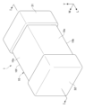
- 1 is a perspective view showing a schematic diagram of a multilayer ceramic capacitor according to an embodiment of the present invention
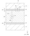
- 2 is a cross-sectional view showing a schematic cross section of the capacitor of FIG. 1 taken along line II.
- 3 is an enlarged cross-sectional view showing a part (area A) of the cross section of FIG. 2 .
- 4 is an example of a line profile along the scan line SL1 in FIG. 3.
- 4 is an example of a line profile along the scan line SL2 in FIG. 3.
- 3 is an enlarged cross-sectional view showing a part (region B) of the cross section of FIG. 2 .
- 3 is an enlarged cross-sectional view showing a part (area C) of the cross section of FIG. 2 .
- FIG. 1 is an example of a line profile obtained by EDS mapping.
- FIG. 2 is a flow chart showing the flow of a method for manufacturing a multilayer ceramic capacitor according to an embodiment of the present invention.
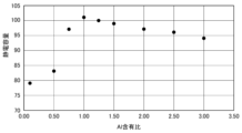
- 4 is a graph for explaining the relationship between the Al content ratio and the capacitance in the internal electrode layers.
- each figure may include an L axis, a W axis, and a T axis that are perpendicular to each other.
- the dimensions, arrangement, shape, and other characteristics of each component of the multilayer ceramic capacitor 1 may be explained based on the L axis, W axis, and T axis.
- Multilayer ceramic capacitor 1 1-1 Basic Structure of Multilayer Ceramic Capacitor 1
- the basic structure of the multilayer ceramic capacitor 1 according to the first embodiment will be described with reference to Figures 1 and 2.
- Figure 1 is a perspective view of the multilayer ceramic capacitor 1 according to the first embodiment.
- Figure 2 is a cross-sectional view that typically shows a cross section of the multilayer ceramic capacitor 1 taken along line II.
- the multilayer ceramic capacitor 1 comprises a body 10, a first external electrode 31 provided on the body 10, and a second external electrode 32.
- the first external electrode 31 is disposed at a distance from the second external electrode 32.
- the first external electrode 31 is disposed at a distance from the second external electrode 32 in the L-axis direction.
- the main body 10 has an upper surface 10a, a lower surface 10b, a first end surface 10c, a second end surface 10d, a first side surface 10e, and a second side surface 10f.
- the outer surface of the main body 10 is defined by the upper surface 10a, the lower surface 10b, the first end surface 10c, the second end surface 10d, the first side surface 10e, and the second side surface 10f.
- the upper surface 10a and the lower surface 10b each form the surfaces at both ends of the main body 10 in the height direction (T axis direction). In other words, the upper surface 10a and the lower surface 10b face each other in the T axis direction.
- the first end surface 10c and the second end surface 10d each form the surfaces at both ends of the main body 10 in the length direction (L axis direction). In other words, the first end surface 10c and the second end surface 10d face each other in the L axis direction.
- the first side surface 10e and the second side surface 10f each form the surfaces at both ends of the main body 10 in the width direction (W axis direction). In other words, the first side surface 10e and the second side surface 10f face each other in the W axis direction.
- the upper surface 10a and the lower surface 10b are spaced apart by the height dimension of the main body 10
- the first end surface 10c and the second end surface 10d are spaced apart by the length dimension of the main body
- the first side surface 10e and the second side surface 10f are spaced apart by the width dimension of the main body 10.
- the main body 10 includes a plurality of dielectric layers 11, a plurality of first internal electrode layers 21, and a plurality of second internal electrode layers 22.
- the dielectric layer 11 is disposed between the first internal electrode layer 21 and the second internal electrode layer 22 adjacent to the first internal electrode layer 21.
- the main body 10 is constructed by stacking the dielectric layers 11, the first internal electrode layers 21, and the second internal electrode layers 22 along the stacking direction.
- the dielectric layers 11, the first internal electrode layers 21, and the second internal electrode layers 22 are stacked along the T-axis direction.
- the stacking direction may be along the T-axis as illustrated, or along the L-axis or W-axis.
- the first internal electrode layers 21 and the second internal electrode layers 22 may be collectively referred to as "internal electrode layers".
- the main body 10 is constructed by stacking the dielectric layer 11, the first internal electrode layer 21, and the second internal electrode layer 22 along the T-axis direction.
- the T-axis direction may be referred to as the stacking direction.
- An upper cover layer 12 may be provided on the upper surface of this stack.
- a lower cover layer 13 may be provided on the lower surface of this stack.
- the upper cover layer 12 and the lower cover layer 13 may be made of the same material as the dielectric layer 11.
- the upper cover layer 12 and the lower cover layer 13 may be part of the main body 10.
- first internal electrode layer 21 is drawn out toward the outside of the main body 10.
- the first internal electrode layer 21 is connected to a first external electrode 31 provided on the surface of the main body 10.
- One end of the second internal electrode layer 22 is drawn out toward the outside of the main body 10.
- the second internal electrode layer 22 is connected to a second external electrode 32 provided on the surface of the main body 10.
- the first internal electrode layer 21 is drawn out toward the outside of the main body 10 from one end in the L-axis direction.
- the first internal electrode layer 21 is connected to the first external electrode 31 at one end of the main body 10 in the L-axis direction.
- the second internal electrode layer 22 is drawn out toward the outside of the main body 10 from the other end in the L-axis direction.
- the second internal electrode layer 22 is connected to the second external electrode 32 at the other end of the main body 10 in the L-axis direction.
- the first internal electrode layer 21 and the second internal electrode layer 22 are drawn out to the opposing first end surface 10c and second end surface 10d, respectively, but the first internal electrode layer 21 and the second internal electrode layer 22 may be drawn out from various surfaces of the main body 10 depending on the arrangement and shape of the first external electrode 31 and the second external electrode 32.
- the first external electrode 31 and the second external electrode 32 are both arranged on the lower surface 10b, the first external electrode 31 and the second external electrode 32 are both drawn out from the lower surface.
- the first external electrode 31 and the second external electrode 32 may be provided on any surface of the main body 10 as long as they are spaced apart from each other.
- a first intermediate layer 41 is disposed between the dielectric layer 11 and the first internal electrode layer 21, and a second intermediate layer 42 is disposed between the dielectric layer 11 and the second internal electrode layer 22, but the first intermediate layer 41 and the second intermediate layer 42 are omitted from illustration in Figures 1 and 2.
- the first intermediate layer 41 and the second intermediate layer 42 may be collectively referred to as "intermediate layer".
- the multilayer ceramic capacitor 1 can have any number of layers.
- the multilayer ceramic capacitor 1 can have 300 to 1000 first internal electrode layers 21 and second internal electrode layers 22. In other words, the number of layers in the multilayer ceramic capacitor 1 can be 300 to 1000.
- the multilayer ceramic capacitor 1 can be mounted on an electronic circuit board.
- An electronic circuit board on which the multilayer ceramic capacitor 1 is mounted is sometimes called a circuit module.
- Various electronic components other than the multilayer ceramic capacitor 1 can also be mounted on the circuit module.
- This circuit module can be mounted on various electronic devices. Electronic devices in which the circuit module can be mounted include smartphones, tablets, game consoles, automotive electrical equipment, servers, and various other electronic devices.
- the body 10 may be configured to have a rectangular parallelepiped shape.
- the term "rectangular parallelepiped” or “rectangular parallelepiped shape” does not mean only a “rectangular parallelepiped” in the strict mathematical sense.
- the corners and/or sides of the body 10 may be curved.
- the dimensions and shape of the body 10 are not limited to those explicitly described in this specification.
- the dimension (length dimension) of the multilayer ceramic capacitor 1 in the L-axis direction is in the range of 0.2 mm to 2.5 mm
- the dimension (width dimension) in the W-axis direction is in the range of 0.1 mm to 3.5 mm
- the dimension (height dimension) in the T-axis direction is in the range of 0.1 mm to 3.0 mm.
- the length dimension of the multilayer ceramic capacitor 1 may be greater than the width dimension.
- the height dimension of the multilayer ceramic capacitor 1 may be greater than the width dimension.
- the width dimension of the capacitor 1 may be greater than the length dimension.
- the dielectric layer 11 contains an oxide represented by the chemical formula ABO3 as a main component. This oxide may have a perovskite structure. A component contained in the dielectric layer 11 at 50 wt% or more based on the total mass of the dielectric layer 11 can be regarded as the main component of the dielectric layer 11.
- the dielectric layer 11 contains an oxide represented by the chemical formula ABO3 at 50 wt% or more, it can be said that the dielectric layer 11 contains an oxide represented by the chemical formula ABO3 as a main component.
- the dielectric layer 11 desirably contains an oxide represented by the chemical formula ABO3 at 60 wt% or more, 70 wt% or more, 80 wt% or more, or 90 wt% or more.
- A is at least one element selected from the group consisting of Ba (barium), Sr (strontium), Ca (calcium), and Mg (magnesium).
- B is at least one element selected from the group consisting of Ti (titanium), Zr (zirconium), and Hf (hafnium).
- oxides contained as a main component in the dielectric layer 11 include BaTiO 3 (barium titanate), CaZrO 3 (calcium zirconate), CaTiO 3 (calcium titanate), SrTiO 3 (strontium titanate), and MgTiO 3 (magnesium titanate).
- the oxide contained as a main component in the dielectric layer 11 may be an oxide represented by the chemical formula Ba1 - xyCaxSryTi1 - zZrzO3 (0 ⁇ x ⁇ 1, 0 ⁇ y ⁇ 1, 0 ⁇ z ⁇ 1).
- this type of oxide include barium strontium titanate, barium calcium titanate, barium zirconate, barium titanate zirconate, calcium titanate zirconate, and barium calcium titanate zirconate.
- the dielectric layer 11 may contain additive elements in addition to the oxides of the main components.
- the additive element contained in the dielectric layer 11 is at least one element selected from the group consisting of Fe (iron), Ni (nickel), Mo (molybdenum), Nb (niobium), Ta (tantalum), W (tungsten), Mg (magnesium), Mn (manganese), V (vanadium), and Cr (chromium).
- the dielectric layer 11 may contain two or more types of the additive elements.
- the dielectric layer 11 may contain an oxide of a rare earth element in addition to the oxide of the main component.
- the oxide of the rare earth element contained in the dielectric layer 11 may be an oxide of at least one rare earth element selected from the group consisting of Y (yttrium), Sm (samarium), Eu (europium), Gd (gadolinium), Tb (terbium), Dy (dysprosium), Ho (holmium), Er (erbium), Tm (thulium), and Yb (ytterbium).
- the dielectric layer 11 may contain two or more types of oxides of rare earth elements.
- the dielectric layer 11 may further contain other types of oxides.
- the dielectric layer 11 may contain an oxide of at least one element selected from the group consisting of Co (cobalt), Ni (nickel), Li (lithium), B (boron), Na (sodium), K (potassium), and Si (silicon).
- the dielectric layer 11 may contain two or more types of oxides of these elements.
- the dielectric layer 11 may contain glass containing at least one element selected from the group consisting of Co, Ni, Li, B, Na, K, and Si.
- the thickness of the dielectric layer 11 (dimension in the T-axis direction) is 0.2 to 10 ⁇ m.
- the first internal electrode layer 21 contains Ni as a main component. Based on the total mass of the first internal electrode layer 21, a component contained in the first internal electrode layer 21 at 50 wt% or more can be the main component of the first internal electrode layer 21.
- the first internal electrode layer 21 desirably contains Ni as the main component at 60 wt% or more, 70 wt% or more, 80 wt% or more, or 90 wt% or more.
- the first internal electrode layer 21 contains Fe and Al in addition to Ni. In one embodiment, the concentration of Fe in the first internal electrode layer 21 is 0.01 at% or more and 5 at% or less.
- the ratio of the Al concentration to the Fe concentration in the first internal electrode layer 21 (hereinafter referred to as the "Al content ratio") is 0.75 or more and 3.0 or less.
- the Al content ratio is preferably 0.75 or more and 2.5 or less.
- the Al content ratio is more preferably 0.75 or more and 1.5 or less.
- the Al content ratio is more preferably 1.0 or more and 1.5 or less.
- the Al content ratio is more preferably 1.0 or more and 1.25 or less.
- the Fe concentration in the first internal electrode layer 21 means the atomic ratio (atomic percentage) (at%) of Fe to 100 at% of Ni contained in the first internal electrode layer 21, and the Al concentration in the first internal electrode layer 21 means the atomic ratio (at%) of Al to 100 at% of Ni contained in the first internal electrode layer 21.
- the first internal electrode layer 21 may contain at least one precious metal element selected from the group consisting of Au (gold), Pt (platinum), and Ag (silver) in addition to N, Fe, and Al.
- the concentration of the above precious metal element in the first internal electrode layer 21 is 0.01 at% or more and 5 at% or less.
- the total concentration of the two or more types of precious metal elements is 0.01 at% or more and 5 at% or less.
- the first internal electrode layer 21 may contain an auxiliary element in addition to or instead of the above-mentioned precious metal element.
- the auxiliary element that may be contained in the first internal electrode layer 21 is, for example, one element or two or more elements selected from the group consisting of As (arsenic), Co, Cr, Cu, Fe, In (indium), Ir (iridium), Mg, Os (osmium), Pd (palladium), Re (rhenium), Rh (rhodium), Ru (ruthenium), Se (selenium), Sn, Ge (germanium), Te (tellurium), W, Y (yttrium), Zn (zinc), and Mo.
- the explanation regarding the components of the first internal electrode layer 21 and the concentration of each component also applies to the components of the second internal electrode layer 22.
- the second internal electrode layer 22 contains Ni as the main component, and in addition to Ni, Fe and Al.
- the explanation regarding the concentration of Fe and Al contained in the first internal electrode layer 21 also applies to the concentration of Fe and Al contained in the second internal electrode layer 22.
- the Al content ratio in the second internal electrode layer 22, which represents the ratio of the concentration of Al to the concentration of Fe in the second internal electrode layer 22, is 0.75 or more and 3.0 or less.
- the Al content ratio in the second internal electrode layer 22 is preferably 0.75 or more and 2.5 or less. It is more preferable that the Al content ratio in the second internal electrode layer 22 is 0.75 or more and 1.5 or less.
- the Al content ratio in the second internal electrode layer 22 is 1.0 or more and 1.5 or less. It is more desirable that the Al content ratio in the second internal electrode layer 22 is 1.0 or more and 1.25 or less.
- the Fe concentration in the second internal electrode layer 22 means the atomic ratio (at%) of Fe to 100 at% of Ni contained in the second internal electrode layer 22
- the Al concentration in the second internal electrode layer 22 means the atomic ratio (at%) of Al to 100 at% of Ni contained in the second internal electrode layer 22.
- the film thickness (dimension in the T-axis direction) of the first internal electrode layer 21 is 0.2 ⁇ m or more and 3 ⁇ m or less. In one embodiment, the film thickness of the first internal electrode layer 21 is desirably 0.4 ⁇ m or less. The explanation regarding the film thickness of the first internal electrode layer 21 also applies to the second internal electrode layer 22.
- the continuity rate of the internal electrode layers in the multilayer ceramic capacitor 1 is desirably 75% or more.
- the continuity rate of the internal electrode layers will be described with reference to FIG. 3.
- FIG. 3 is an enlarged cross-sectional view showing an enlarged region A of the cross section of the main body 10 shown in FIG. 2.
- Region A is an area with a dimension L0 in the L-axis direction of about 50 ⁇ m.
- the first internal electrode layer 21 includes a plurality of electrode regions 21a containing Ni and non-electrode regions 21b present between the electrode regions 21a.
- the non-electrode regions 21b are regions with higher insulating properties than the electrode regions 21a.
- the non-electrode regions 21b are occupied by, for example, oxides of elements contained in the first internal electrode layer 21, parts of the dielectric layer 11, and/or voids.
- the non-electrode regions 21b may be formed when the binder resin contained in the precursor of the first internal electrode layer 21 is vaporized during the degreasing process of the precursor of the first internal electrode layer 21, or when the elements contained in the precursor of the first internal electrode layer 21 are oxidized during firing.
- the first internal electrode layer 21 contains Fe and Al in an appropriate ratio, a segregation portion containing Fe and Al is generated. The segregation portion will be described later. If the first internal electrode layer 21 contains an excess of Al relative to Fe, it may be oxidized during firing to generate insulating aluminum oxide. The aluminum oxide produced in this manner may also occupy part of the non-electrode region 21b.
- the continuity rate of the first internal electrode layer 21 can be calculated as follows. First, the multilayer ceramic capacitor 1 is polished so that the LT surface becomes the observation surface. Next, the region A included in this observation surface is observed with an SEM (scanning electron microscope), and the distribution regions of Ni, Fe, Al, and O are examined by EDS mapping. From the distribution of Ni, Fe, and Al and the distribution of O, the region that does not overlap with O is identified as the electrode region 21a made of metal. Then, the length of this electrode region 21a is measured, and the side lengths L1, L2, ..., Ln are summed.
- the value obtained by dividing the sum of the lengths of the electrode regions 21a in this region A by the length L0 of the measurement region can be defined as the continuity rate of one first internal electrode layer 21.
- the main body 10 includes a plurality of first internal electrode layers 21, and the continuity rate can vary depending on which layer of the plurality of first internal electrode layers 21 is focused on. Therefore, ten different first internal electrode layers 21 are selected, and the average of the continuity rates calculated for each of the selected first internal electrode layers 21 can be defined as the continuity rate of the first internal electrode layers 21 in the multilayer ceramic capacitor 1.
- the second internal electrode layer 22 can also be divided into an electrode region and a non-electrode region. Specifically, as shown in FIG. 3, the second internal electrode layer 22 includes a plurality of electrode regions 22a containing a main component metal element, and non-electrode regions 22b existing between the electrode regions 22a.
- the continuity rate of the second internal electrode layer 22 is defined in the same manner as the continuity rate of the first internal electrode layer 21.
- the average of the continuity rates of the first internal electrode layer 21 and the second internal electrode layer 22 can be taken as the continuity rate of the internal electrode layers in the multilayer ceramic capacitor 1.
- the multilayer ceramic capacitor 1 capacitance is generated in the region where the electrode region 21a of the first internal electrode layer 21 and the electrode region 22a of the second internal electrode layer 22 face each other in the stacking direction. Conversely, the non-electrode region 21b and the non-electrode region 22b do not generate capacitance. Therefore, in order to achieve a high capacity in the multilayer ceramic capacitor 1, it is desirable that the continuity rate of the internal electrode layers is high. In one embodiment, the continuity rate of the internal electrode layers is 75% or more. This makes it possible to obtain a multilayer ceramic capacitor 1 with high capacity.
- the first internal electrode layer 21 may contain a segregation portion 25 in which both Fe and Al are segregated.
- the segregation portion 25 is a region occupying a part of the first internal electrode layer 21, and contains Fe and Al at a higher concentration than other regions of the first internal electrode layer 21.
- the first internal electrode layer 21 may have a plurality of segregation portions 25.
- the segregation portion 25 may have a minor axis that is 1/10 or more of the film thickness of the first internal electrode layer 21. For example, when the film thickness of the first internal electrode layer 21 is 0.2 ⁇ m, the minor axis of the segregation portion 25 is 20 nm or more.
- Fe and Al may be alloyed. The presence of the segregation portion 25 in the first internal electrode layer 21 can be confirmed as follows.
- the multilayer ceramic capacitor 1 is embedded in resin, and the multilayer ceramic capacitor 1 embedded in the resin is polished to near the center in the W-axis direction so that the LT surface becomes the observation surface.
- the cross section of the multilayer ceramic capacitor 1 exposed by this polishing is observed at a magnification of 5000 times with an SEM (scanning electron microscope) equipped with an EDS detector, and a mapping image of the quantified elements is obtained.
- the quantified elements are Ni, Fe, Al, and Ba.
- the intensities of the Ni K ⁇ line, Fe K ⁇ line, Al K line, and Ba L ⁇ line are measured to obtain mapping data of the quantified elements.
- a line analysis is performed based on the acquired mapping data. For example, as shown in FIG. 3, a line profile is created for each of the quantitative elements by reconstructing the mapping data of the quantitative elements along the scanning lines SL1 and SL2 that extend in the T-axis direction and straddle the first internal electrode layer 21.
- the scanning line SL1 passes through the segregation portion 25 generated in the first internal electrode layer 21, and the scanning line SL2 passes through an area of the first internal electrode layer 21 where the segregation portion 25 is not formed.
- the lengths of the scanning lines SL1 and SL2 are, for example, 1 ⁇ m to 1.5 ⁇ m. The lengths of the scanning lines SL1 and SL2 can be changed depending on the film thickness of the first internal electrode layer 21.
- FIG. 4 shows an example of a line profile in which mapping data is reconstructed along the scan line SL1
- FIG. 5 shows an example of a line profile in which mapping data is reconstructed along the scan line SL2.
- the horizontal axis indicates the detection position on the scan line SL1 and the scan line SL2, respectively
- the vertical axis indicates the detection intensity calculated based on the count number of each of Ni, Fe, Al, and Ba at each detection position.
- the detection intensity of Ni exceeds the detection intensity of Ba from a position about 0.2 ⁇ m to a position about 0.7 ⁇ m from the scanning start position, so the region between this 0.2 ⁇ m position and about 0.7 ⁇ m corresponds to the first internal electrode layer 21.
- FIG. 4 shows an example of a line profile in which mapping data is reconstructed along the scan line SL1
- the vertical axis indicates the detection intensity calculated based on the count number of each of Ni, Fe, Al, and Ba at each detection position.
- the detection intensity of Ni exceeds the
- the detection intensity of Ni exceeds the detection intensity of Ba from a position about 0.3 ⁇ m to a position about 1.1 ⁇ m from the scanning start position, so the region between this 0.3 ⁇ m position and about 1.1 ⁇ m corresponds to the first internal electrode layer 21.
- the detection intensities of Fe and Al are generally constant even in the first internal electrode layer 21 where the detection intensity of Ni is higher than the detection intensity of Ba.
- the detection intensities of Fe and Al also increase in the region in the first internal electrode layer 21 where the detection intensity of Ni is higher than the detection intensity of Ba.
- the peak of the detection intensity of Ni in the region in the first internal electrode layer 21 shown in Fig. 4 is smaller than the peak of the detection intensity of Ni in the region in the first internal electrode layer 21 shown in Fig. 5.
- the detection intensity of Ni is low in the region in the first internal electrode layer 21, while the detection intensities of Fe and Al are high, so that it can be confirmed that the segregation portion 25 is generated in the region through which the scanning line SL1 passes.
- a first intermediate layer 41 in which Fe is concentrated is formed between the first internal electrode layer 21 and the dielectric layer 11, but in the line profiles shown in Figures 4 and 5, no Fe peak is observed at the boundary between the first internal electrode layer 21 and the dielectric layer 11 due to the resolution limit.
- the fact that no Fe peak appears at the boundary between the first internal electrode layer 21 and the dielectric layer 11 is due to the resolution limit during EDS mapping, and does not mean that the first intermediate layer 41 does not exist between the first internal electrode layer 21 and the dielectric layer 11.
- the content of Fe and Al in the first internal electrode layer 21 is minute compared to Ni, it is possible that a clear peak like that of Ni cannot be confirmed in the line profile of Fe and Al constructed along the scan line passing through the segregation portion 25.
- the first internal electrode layer 21 includes an area where the detection intensity of Fe and the detection intensity of Al are both 5 times or more the square root of their respective background levels, it can be determined that the area is a segregation portion 25 where both Fe and Al are segregated.
- the line profile shown in Figure 4 indicates that a segregation portion 25 exists on the scan line SL1.
- the line profile shown in Figure 5 indicates that a segregation portion 25 does not exist on the scan line SL2.
- the segregation portion 25 is considered to be a metal portion that contains both Fe and Al, and is therefore considered to have electrical conductivity. Therefore, by including the segregation portion 25 in the first internal electrode layer 21, the continuity rate of the first internal electrode layer 21 can be improved.
- the segregation portion 25 may be generated in the second internal electrode layer 22.
- the segregation portion 25 may be generated in both the first internal electrode layer 21 and the second internal electrode layer 22.
- the segregation portion 25 may be formed in each of the multiple first internal electrode layers 21, or may be generated in only a part of the multiple first internal electrode layers 21.
- the segregation portion 25 may be formed in each of the multiple second internal electrode layers 22, or may be generated in only a part of the multiple second internal electrode layers 22.
- the segregation portion 25 may be generated so as to penetrate the first internal electrode layer 21 or the second internal electrode layer 22 in the stacking direction.
- the segregation portion 25 may be embedded inside the first internal electrode layer 21 or the second internal electrode layer 22. A part of the segregation portion 25 may be exposed from the first internal electrode layer 21 or the second internal electrode layer 22.
- First external electrode 31 and second external electrode 32 are formed by applying a conductive paste to the main body 10 and heating the conductive paste.
- the conductive paste may include at least one material selected from the group consisting of Ag, Pd, Au, Pt, Ni, Sn, Cu, W, Ti, and alloys thereof.
- FIG. 6 is an enlarged cross-sectional view showing an enlarged region B of the cross section of the main body 10 shown in Fig. 2.
- Region B is a region including one of the multiple first internal electrode layers 21 provided in the main body 10 and the dielectric layers 11 located above and below the first internal electrode layer 21. In other words, region B extends from the dielectric layer 11 located below the first internal electrode layer 21 through the first internal electrode layer 21 to the dielectric layer 11 located above the first internal electrode layer 21.
- a first intermediate layer 41 is provided between the dielectric layer 11 and the first internal electrode layer 21.
- the first intermediate layer 41 contains Fe.
- the concentration of Fe in the first intermediate layer 41 is higher than the concentration of Fe in the first internal electrode layer 21.
- the first intermediate layer 41 may also contain Al.
- the first intermediate layer 41 which contains Fe at a higher concentration than the first internal electrode layer 21, can increase the Schottky barrier formed between the dielectric layer 11 and the first internal electrode layer 21.
- the increase in leakage current can be suppressed, and as a result, the insulation reliability of the multilayer ceramic capacitor 1 can be improved. In other words, the life of the multilayer ceramic capacitor 1 can be extended.
- Al when the first intermediate layer 41 contains Al, Al can also increase the Schottky barrier formed between the dielectric layer 11 and the first internal electrode layer 21, just like Fe. Therefore, by having the first intermediate layer 41 contain Al, the insulation reliability of the multilayer ceramic capacitor 1 can be further improved.
- FIG. 7 is an enlarged cross-sectional view showing an enlarged region C of the cross section of the main body 10 shown in FIG. 2.
- Region C is a region including one of the multiple second internal electrode layers 22 provided in the main body 10 and the dielectric layer 11 located above or below the second internal electrode layer 22.
- the second intermediate layer 42 is provided between the dielectric layer 11 and the second internal electrode layer 22.
- the second intermediate layer 42 contains Fe. In one embodiment, the concentration of Fe in the second intermediate layer 42 is higher than the concentration of Fe in the second internal electrode layer 22.
- the second intermediate layer 42 may also contain Al. The second intermediate layer 42 can increase the Schottky barrier formed between the dielectric layer 11 and the second internal electrode layer 22.
- the increase in leakage current can be suppressed, and as a result, the insulation reliability of the multilayer ceramic capacitor 1 can be improved. In other words, the life of the multilayer ceramic capacitor 1 can be extended.
- the thickness t41 (dimension in the T-axis direction) of the first intermediate layer 41 is, for example, 0.2 nm or more and 3.0 nm or less.
- the lower limit of the thickness t41 of the first intermediate layer 41 may be 0.3 nm, 0.4 nm, or 0.5 nm.
- the upper limit of the thickness t41 of the first intermediate layer 41 may be 2.0 nm, 1.5 nm, or 1.3.
- the thickness t42 of the second intermediate layer 42 may be approximately the same as the thickness t41 of the first intermediate layer 41.
- the main body 10 includes a first intermediate layer 41 and a second intermediate layer 42. Therefore, the Schottky barrier can be increased in both sections between the dielectric layer 11 and the first internal electrode layer 21 and between the dielectric layer 11 and the second internal electrode layer 22.
- the main body 10 includes the first intermediate layer 41 but does not necessarily include the second intermediate layer 42. In this case, the Schottky barrier between the dielectric layer 11 and the first internal electrode layer 21 can be increased.
- the main body 10 includes the second intermediate layer 42 but does not necessarily include the first intermediate layer 41. In this case, the Schottky barrier between the dielectric layer 11 and the second internal electrode layer 22 can be increased.
- the first intermediate layer 41 may cover the entire first internal electrode layer 21.
- the first intermediate layer 41 may cover only a portion of the first internal electrode layer 21. It is desirable that the first intermediate layer 41 cover 80% or more of the entire area of the upper and lower surfaces of the first internal electrode layer 21 in order to suppress leakage current.
- the second intermediate layer 42 may cover the entire second internal electrode layer 22.
- the second intermediate layer 42 may cover only a portion of the second internal electrode layer 22. It is desirable that the second intermediate layer 42 cover 80% or more of the entire area of the upper and lower surfaces of the second internal electrode layer 22 in order to suppress leakage current.
- an observation region extending from the first internal electrode layer 21 to the dielectric layer 11 is set in the cross section of the main body 10, and the presence of the first intermediate layer 41 can be confirmed based on mapping data of Fe elements obtained by performing TEM-EDS on this observation region.
- Detection of the first intermediate layer 41 by TEM-EDS analysis can be performed, for example, as follows. (1) First, the main body 10 is sliced to prepare an analysis sample so that a plane parallel to a plane (for example, an LT plane) including the T axis becomes the observation surface, and an observation area extending from the first internal electrode layer 21 to the dielectric layer 11 is set on the observation surface of the sliced analysis sample.
- the observation area B1 in FIG. 6 is an example of an observation area by TEM-EDS analysis. TEM-EDS is performed on this observation area B1 to obtain mapping data of the quantified elements contained in the observation area B1 of the analysis sample.
- the observation area B1 is, for example, a square area of 15 nm on each side.
- the quantified elements include elements contained in the main component oxide of the dielectric layer 11 (for example, Ba, Ti, O when the main component oxide is BaTiO 3 ), Ni, and Fe.
- the quantified elements may include Al.
- a line profile is created for each of the quantitative elements by reconstructing the mapping data of the quantitative elements along a scanning line SL3 extending from the first internal electrode layer 21 to the dielectric layer 11 in the observation region B1.
- the length of the scanning line SL3 is, for example, 8 nm.
- the length of the scanning line SL3 for obtaining the line profile can be changed as appropriate.
- FIG. 8 shows an example of a line profile in which the mapping data acquired by TEM-EDS in the region A1 of the analysis sample is reconstructed along the scanning line SL3.
- FIG. 8 is an example of a graph in which the mapping data of each element of Ba, Ti, O , Ni, and Fe obtained by performing TEM-EDS on an analysis sample created from a multilayer ceramic capacitor 1 whose dielectric layer 11 is mainly composed of BaTiO 3 is reconstructed along the scanning line SL.
- the horizontal axis indicates the detection position on the scanning line SL1
- the vertical axis indicates the detection intensity calculated based on the count number of each of Ba, Ti, O, Ni, and Fe at each detection position.
- profile intersection When a peak of the line profile of Fe exists near the intersection (hereinafter referred to as "profile intersection") where the line profile of an element other than oxygen (e.g., Ba) of the main component oxide of the dielectric layer 11 and the line profile of the main component metal element of the first internal electrode layer 21 intersect, it can be determined that the first intermediate layer 41 exists in the multilayer ceramic capacitor 1 from which the analysis sample was taken.
- a predetermined threshold value can be, for example, 1 nm, 0.9 nm, 0.8 nm, 0.7 nm, 0.6 nm, or 0.5 nm.
- the line profile of Ba of BaTiO3 contained as a main component in the dielectric layer 11 and the line profile of Ni contained as a main component in the first internal electrode layer 21 intersect at a position about 4.1 nm from the scanning start position.
- the profile intersection point 52 where the line profile of Ba and the line profile of Ni intersect is located at a position about 4.1 nm from the scanning start position.
- a peak 51 of the line profile of Fe is present at a position about 3.9 nm from the scanning start position. Since the peak 51 of the line profile of Fe is located at a position about 0.2 nm away from the profile intersection point 52, which is smaller than the threshold value, it is determined that the first intermediate layer 41 is present in the region including this peak 51.
- the line profile shown in FIG. 8 has a significantly different resolution from the line profiles shown in FIG. 4 and FIG. 5.
- the line profile in FIG. 8 is created by reconstructing a concentration map along a scan line SL3 of 8 nm
- the line profiles in FIG. 4 and FIG. 5 are created by reconstructing a concentration map along scan lines SL1 and SL2 of 1 ⁇ m or more in length. Due to this difference in resolution, in FIG. 4 and FIG. 5, the peak of the Fe line profile cannot be clearly confirmed near the intersection of the Ni line profile and the Ba line profile.
- FIG. 4 and FIG. 5 the peak of the Fe line profile cannot be clearly confirmed near the intersection of the Ni line profile and the Ba line profile.
- Fig. 9 is a flow chart showing the flow of a method for manufacturing a multilayer ceramic capacitor according to an embodiment of the present invention.
- step S11 a binder such as polyvinyl butyral (PVB) resin, an organic solvent such as ethanol or toluene, and a plasticizer are first added to the dielectric powder and wet mixed to obtain a slurry.
- This slurry is then applied to a substrate film by, for example, a die coater method or a doctor blade method, and the slurry applied to the substrate film is dried to obtain a dielectric green sheet.
- the dielectric green sheet is a precursor of the dielectric layer 11.
- the dielectric powder which is the raw material powder for the dielectric green sheet, is, for example, barium titanate powder.
- Barium titanate powder is synthesized by reacting a titanium raw material such as titanium dioxide with a barium raw material such as barium carbonate using a known method such as the solid-phase method, the sol-gel method, or the hydrothermal method.
- the internal electrode patterns are formed on the plurality of dielectric green sheets formed as described above.
- the internal electrode patterns are formed, for example, by printing the internal electrode paste on the dielectric green sheets by a known printing method such as screen printing.
- the internal electrode paste is manufactured by kneading a metal powder, a binder resin, and a solvent with a three-roll mill. That is, the internal electrode paste is a paste in which the metal powder is dispersed in the solvent.
- the metal powder contained in the internal electrode paste may be a mixed powder in which Ni powder is mixed with an Fe-containing powder containing Fe and an Al-containing powder containing Al.
- the Fe-containing powder is, for example, Fe 2 O 3 powder.
- the metal powder contained in the internal electrode paste may be a composite particle generated by putting Ni powder into an organic solvent in which an aluminum resinate is dissolved, dispersing the Ni powder in the solution, and then evaporating the solvent.
- the composite particle generated in this manner is a particle in which Al is dispersed and attached to the surface of the Ni particle.
- the metal powder contained in the internal electrode paste may be a powder of an alloy of Ni and Al.
- the metal powder contained in the internal electrode paste may be a coating powder in which a coating layer containing Al is formed on the surface of Ni.
- the Al-containing powder is, for example, Al 2 O 3 powder.
- the mixed powder is produced by weighing the Fe-containing powder so that the content ratio of Fe relative to 100 at% of Ni is in the range of 0.01 to 10 at%, and also weighing the Al-containing powder so that the content ratio of Al relative to 100 at% of Ni is in the range of 0.01 to 10 at%, and mixing the weighed Fe-containing powder and Al-containing powder with Ni powder.
- a cellulose-based resin such as ethyl cellulose or an acrylic-based resin such as butyl methacrylate can be used.
- the internal electrode pattern formed on some of the dielectric green sheets is a precursor of the first internal electrode layer 21, and the internal electrode pattern formed on the other dielectric green sheets is a precursor of the second internal electrode layer 22.
- the internal electrode pattern may be formed on the dielectric green sheet by a sputtering method.
- the method of forming the internal electrode pattern is not limited to the methods specifically described in this specification.
- the internal electrode pattern may be formed by various known methods, such as vacuum deposition, PLD (pulsed laser deposition), MO-CVD (metal organic chemical vapor deposition), MOD (metal organic decomposition), or CSD (chemical solution deposition).
- a laminate unit that has a dielectric green sheet and an internal electrode pattern formed on the surface of the dielectric green sheet.
- a predetermined number of these laminate units are stacked and thermocompressed to obtain a laminate.
- Green sheets that do not have an internal electrode pattern formed thereon may be stacked on the top and bottom layers of the laminate.
- a chip-shaped laminate that serves as a precursor of the main body 10 is obtained.
- a degreasing process may be performed on this chip-shaped laminate.
- the degreasing process may be performed in an N2 atmosphere.
- a metal paste that serves as the base electrode layer of the first external electrode 31 and the second external electrode 32 may be applied by a dipping method to the degreased laminate.
- step S12 the chip stack produced in step S11 is placed in a sintering furnace, and the stack is sintered in the sintering furnace according to a predetermined temperature profile, thereby obtaining the multilayer ceramic capacitor 1.
- the inside of the sintering furnace is maintained in a low-oxygen atmosphere, for example, with an oxygen partial pressure of 10 -12 to 10 -10 atm.
- the temperature in the sintering furnace is raised from room temperature to the sintering start temperature at a rate of 200 to 1000°C/h, and is held at this sintering start temperature for 10 minutes to 1 hour. That is, in the sintering process, the chip stack is heated at the sintering start temperature for about 10 minutes to 1 hour.
- the sintering start temperature is set to 850 to 1100°C at which Ni can be sintered.
- the temperature in the sintering furnace is raised at a high heating rate from the sintering start temperature to the sintering top temperature.
- the sintering top temperature is, for example, 1150 to 1300°C.
- the temperature rise rate is, for example, 3000 to 10000° C./h.
- the temperature inside the firing furnace is held at the firing top temperature for 10 to 30 minutes, and then the inside of the firing furnace is cooled. In this manner, the chip stack is fired to obtain a fired body.
- the dielectric green sheets in the chip stack are fired to become the dielectric layers 11, and the internal electrode patterns are fired to become the internal electrode layers (first internal electrode layer 21 and second internal electrode layer 22).
- Fe contained in the internal electrode patterns is thermally diffused toward the interface with the dielectric green sheets. Therefore, in the multilayer ceramic capacitor 1, a first intermediate layer 41 and a second intermediate layer 42 containing Fe at a higher concentration than the internal electrode layers are formed between the dielectric layer 11 and the first internal electrode layer 21 and between the second internal electrode layer 22, respectively.
- the first intermediate layer 41 and the second intermediate layer 42 also contain Al.
- the multilayer ceramic capacitor 1 obtained by the second heating process in step S12 may be subjected to a reoxidation process at 600°C to 1000°C in an N2 gas atmosphere.
- a plating layer of Cu, Ni, Sn, or the like may be provided on the surfaces of the first external electrode 31 and the second external electrode 32. This plating layer may be formed by electrolytic plating or electroless plating.
- Example 1 The present invention will be described in more detail below with reference to examples, but the present invention is not limited to the following examples.
- a predetermined amount of Fe2O3 powder and Al2O3 powder were weighed into the Ni powder , and the weighed Fe2O3 powder and Al2O3 powder were mixed with the Ni powder to prepare a mixed powder.
- the added amount of Fe2O3 powder and Al2O3 powder was adjusted so that the concentration in the internal electrode layer after firing was the concentration shown in Table 1. Note that neither Fe2O3 powder nor Al2O3 powder was added to the internal electrode slurry for preparing sample 14, only Fe2O3 powder was added to the internal electrode slurry for preparing sample 15, and only Al2O3 powder was added to the internal electrode slurry for preparing sample 16 .
- PVB polyvinyl butyral
- This laminated unit has a dielectric green sheet and an internal electrode pattern formed on the surface of the dielectric green sheet.
- the chip stack had a 1005 shape (length: 1.0 mm, width: 0.5 mm, height: 0.5 mm).
- this chip stack was degreased in an N2 atmosphere.
- a metal paste was applied to the molded body after the degreasing process using a dipping method to form an external electrode base layer on each chip stack.
- samples 1 to 16 are all multilayer ceramic capacitors.
- each of Samples 1 to 16 was sliced by a focused ion beam (FIB) so that the LT surface (FIG. 2) was the observation surface, and a sliced analysis sample with a thickness of 60 nm was taken out from each of Samples 1 to 16. Damage that appeared on the observation surface of the sliced sample was appropriately removed by Ar ion milling.
- the sliced sample was placed in an STEM equipped with an EDS detector, and a STEM image was obtained on the observation surface of the sliced sample, and the internal electrode layer was identified based on the difference in contrast of this STEM image.
- a JEM-2100F manufactured by JEOL Ltd. was used as a TEM for obtaining the STEM image.
- a dry SD100GV detector manufactured by JEOL Ltd. was used as an EDS detector.
- a concentration map was obtained in each observation region, which represents the concentration of the quantitative elements (Ba, Ti, O, Ni, Fe, and Al) in atomic ratio (at%), and this concentration map was reconstructed along a scanning line SL set to extend from the internal electrode layer to the dielectric layer along the T-axis in each observation region B1, thereby obtaining a line profile of each quantitative element for each observation region.
- the peak of Fe appeared near the intersection of the Ba profile and the Ni profile, roughly similar to FIG. 8.
- an Al peak appeared near the intersection of the Ba profile and the Ni profile.
- neither an Fe peak nor an Al peak was detected.
- Capacitance The capacitance was measured for each of Samples 1 to 16. The capacitance was measured using an LCR meter under the conditions of room temperature, a measurement voltage of 0.5 V, and a frequency of 1 kHz. 100 samples were selected for each of Samples 1 to 16, and the capacitance was determined for each of the 100 samples. The average value of the capacitance measured for the 100 samples for each sample was calculated, and this calculated average value was taken as the capacitance of the sample. The capacitance calculated in this manner is listed in the "Capacitance" column of Table 1. The capacitances listed in Table 1 represent the relative capacitance of each sample when the capacitance of Sample 14, to which neither Fe nor Al is added, is taken as the standard (100). For example, the capacitance of Sample 1, "79", means that the capacitance calculated for Sample 1 is 79% of the capacitance of Sample 14.
- Insulation Reliability 100 samples were selected from each of Samples 1 to 14, and an accelerated life test (HALT) was performed on each of the selected samples.
- HALT accelerated life test
- the failure time was determined when a voltage of 6 V/ ⁇ m was applied at 125° C. for each of the 100 samples selected for each of Samples 1 to 14.
- the median failure time determined for the 100 samples was taken as the HALT50% value for each sample.
- the relative HALT50% value of each sample was calculated when the HALT50% value of Sample 14, to which neither Fe nor Al was added, was taken as the reference (100), and the relative HALT50% value calculated in this manner was listed in the “Reliability” column of Table 1.
- the reliability “158” of Sample 1 means that the HALT50% value calculated for Sample 1 is 158% of the HALT50% value of Sample 14.
- Sample 15 is Compared to sample 14, the insulation reliability is improved by 55%, but the capacitance is reduced by 25%.
- the reason why the insulation reliability of sample 15 is significantly improved compared to sample 14 is believed to be because Fe diffuses to the interface between the dielectric layer and the internal electrode layer during firing, and an intermediate layer containing Fe at a high concentration is formed between the dielectric layer and the internal electrode layer, and this intermediate layer enhances the Schottky barrier between the dielectric layer and the internal electrode layer.
- the reason why the capacitance is significantly reduced in sample 15 is believed to be because Fe diffuses into the dielectric layer during firing, and the Fe in the dielectric layer inhibits polarization reversal of barium titanate.
- sample 16 has a 5% improvement in insulation reliability, but a 5% decrease in capacitance.
- the reason that sample 16 has improved insulation reliability compared to sample 14 is thought to be that Al diffuses slightly to the interface between the dielectric layer and the internal electrode layer during firing, and the Al present at this interface strengthens the Schottky barrier between the dielectric layer and the internal electrode layer.
- the reason that the capacitance of sample 16 has decreased is thought to be that Al has oxidized in the internal electrode layer, producing insulating aluminum oxide.
- the reason that the decrease in capacitance and the improvement in insulation reliability of sample 16 are lower than those of sample 14 is thought to be that Al is less susceptible to thermal diffusion than Fe in the environment in which multilayer ceramic capacitors are manufactured.
- sample 4 in which the internal electrode layer contains the same amount of Fe as sample 15 and the same amount of Al as sample 16, the insulation reliability is improved by 104% and the capacitance is improved by 1% compared to sample 14. In other words, in sample 4, both the capacitance and the insulation reliability are improved compared to sample 14.
- One of the reasons for the improved capacitance in sample 4 is that Fe is bonded to Al in the internal electrode layer, which suppresses the diffusion of Fe into the dielectric layer and suppresses the decrease in capacitance due to the increase in Fe concentration in the dielectric layer.
- the bonding of Fe and Al creates a conductive segregation portion 25 in the internal electrode layer, and the continuity rate of the internal electrode layer is improved by the amount of this segregation portion 25, which is another reason for the improved capacitance of sample 4.
- the insulation reliability is improved in sample 4 because Fe that did not bond with Al during firing diffuses to the interface between the dielectric layer and the internal electrode layer, and the Schottky barrier between the dielectric layer and the internal electrode layer is increased.
- samples 10 to 13 contain Fe and Al in the internal electrode layer at the same concentration.
- the Al content ratio is 1.0 in all of samples 10 to 13.
- samples 10 to 12 have improved capacitance and insulation reliability compared to sample 14.
- Sample 13 has a capacitance of 98, which is slightly lower than sample 14, but the degree of decrease can be evaluated as being slight compared to the capacitance of sample 15, which does not contain Al, which is 75. In this way, it was confirmed that samples 10 to 13, which contain Fe and Al in the internal electrode layer at the same concentration, have both excellent capacitance and insulation reliability. The reason why samples 10 to 13 have both excellent capacitance and insulation reliability is thought to be the same as sample 4.
- the reason why the capacitance is significantly decreased in the region where the Al content is smaller than 0.75 is thought to be because when the Fe content is slightly higher than the Al content (when the Al content is 0.75 or more and less than 1.0), the Fe that thermally diffuses toward the dielectric layer remains at the interface between the internal electrode layer and the dielectric layer and forms an intermediate layer at that interface.
- the Fe content is excessive compared to the Al content (when the Al content ratio is less than 0.75)
- the graph in FIG. 10 also confirms that the capacitance tends to decrease as the Al content increases beyond 1.
- the degree of decrease in capacitance in regions where the Al content is greater than 1 is smaller than the degree of decrease in capacitance in regions where the Al content is greater than 1. In other words, the capacitance decreases more slowly in regions where the Al content is greater than 1 than in regions where the Al content is less than 1.
- Example 2 The mixed powder used in the preparation of the above-mentioned sample 4 was mixed with a precious metal powder to produce a mixed powder, and the mixed powder containing the precious metal powder was used to obtain an internal electrode slurry in the same manner as in sample 4. Using this internal electrode slurry, a multilayer ceramic capacitor was prepared in the same manner as in sample 4.
- the precious metal powders used were Au, Ag, and Pt.
- the amount of the precious metal powder added was adjusted so that the concentration of the precious metal in the internal electrode layer after firing was 1.0 at%, which was the same amount as Fe and Al.
- the capacitance and HALT50% value were measured under the same conditions as in Example 1.
- the multilayer ceramic capacitor to which the Au powder was added had a capacitance of 120 and a HALT50% value of 350.
- the capacitance was 110 and the HALT50% value was 275.
- the capacitance was 115 and the HALT50% value was 310. In this way, it was confirmed that by making the internal electrode layers contain Au, Ag, or Pt at the same concentration as Fe and Al, both the capacitance and the insulation reliability were improved.
- the designations "first,” “second,” “third,” and the like are used to identify components, and do not necessarily limit the number, order, or content. Furthermore, numbers for identifying components are used in different contexts, and a number used in one context does not necessarily indicate the same configuration in another context. Furthermore, there is no prohibition on a component identified by a certain number also serving the function of a component identified by another number.
- the Al content is 0.75 or more and 2.5 or less.
- [Appendix 3] The Al content is 0.75 or more and 1.5 or less.
- [Appendix 4] The Al content is 1.0 or more and 1.5 or less.
- [Appendix 5] The concentration of Fe in the first internal electrode layer is 0.01 at% or more and 5 at% or less.
- [Appendix 6] The concentration of Fe in the first internal electrode layer is 0.1 at% or more and 5 at% or less.
- the first internal electrode layer 21 includes a segregation portion in which Fe and Al are segregated.
- the first internal electrode layer contains at least one precious metal element selected from the group consisting of Au, Pt, and Ag.
- the concentration of the precious metal in the first internal electrode layer is 0.01 at% or more and 5 at% or less.
- the second internal electrode layer contains Ni, Fe, and Al
- the body further includes a second intermediate layer containing Fe and Al between the second internal electrode layer and the dielectric layer, an Al content ratio, which represents a ratio of an Al concentration to an Fe concentration in the second internal electrode layer, is 0.75 or more and 3.0 or less;
- the multilayer ceramic capacitor according to any one of [Appendix 1] to [Appendix 9].
- Appendix 11 A circuit module comprising the multilayer ceramic capacitor according to any one of [Appendix 1] to [Appendix 10].
- [Appendix 12] An electronic device comprising the circuit module according to [Supplementary Note 11].
Landscapes
- Engineering & Computer Science (AREA)
- Power Engineering (AREA)
- Manufacturing & Machinery (AREA)
- Microelectronics & Electronic Packaging (AREA)
- Chemical & Material Sciences (AREA)
- Materials Engineering (AREA)
- Ceramic Engineering (AREA)
- Inorganic Chemistry (AREA)
- Fixed Capacitors And Capacitor Manufacturing Machines (AREA)
Priority Applications (3)
| Application Number | Priority Date | Filing Date | Title |
|---|---|---|---|
| JP2025506566A JPWO2024190168A1 (https=) | 2023-03-16 | 2024-02-05 | |
| CN202480019348.7A CN120814013A (zh) | 2023-03-16 | 2024-02-05 | 层叠陶瓷电容器和层叠陶瓷电容器的制造方法 |
| US19/329,318 US20260011495A1 (en) | 2023-03-16 | 2025-09-15 | Laminated ceramic capacitor |
Applications Claiming Priority (2)
| Application Number | Priority Date | Filing Date | Title |
|---|---|---|---|
| JP2023-042427 | 2023-03-16 | ||
| JP2023042427 | 2023-03-16 |
Related Child Applications (1)
| Application Number | Title | Priority Date | Filing Date |
|---|---|---|---|
| US19/329,318 Continuation US20260011495A1 (en) | 2023-03-16 | 2025-09-15 | Laminated ceramic capacitor |
Publications (1)
| Publication Number | Publication Date |
|---|---|
| WO2024190168A1 true WO2024190168A1 (ja) | 2024-09-19 |
Family
ID=92755114
Family Applications (1)
| Application Number | Title | Priority Date | Filing Date |
|---|---|---|---|
| PCT/JP2024/003779 Ceased WO2024190168A1 (ja) | 2023-03-16 | 2024-02-05 | 積層セラミックコンデンサ及び積層セラミックコンデンサの製造方法 |
Country Status (4)
| Country | Link |
|---|---|
| US (1) | US20260011495A1 (https=) |
| JP (1) | JPWO2024190168A1 (https=) |
| CN (1) | CN120814013A (https=) |
| WO (1) | WO2024190168A1 (https=) |
Citations (2)
| Publication number | Priority date | Publication date | Assignee | Title |
|---|---|---|---|---|
| JPH1081924A (ja) * | 1996-07-11 | 1998-03-31 | Philip Morris Prod Inc | 元素状粉末の熱化学処理による鉄アルミナイドの製造方法 |
| JP2013135096A (ja) * | 2011-12-27 | 2013-07-08 | Tdk Corp | 電極焼結体、積層電子部品、内部電極ペースト、電極焼結体の製造方法、積層電子部品の製造方法 |
-
2024
- 2024-02-05 JP JP2025506566A patent/JPWO2024190168A1/ja active Pending
- 2024-02-05 CN CN202480019348.7A patent/CN120814013A/zh active Pending
- 2024-02-05 WO PCT/JP2024/003779 patent/WO2024190168A1/ja not_active Ceased
-
2025
- 2025-09-15 US US19/329,318 patent/US20260011495A1/en active Pending
Patent Citations (2)
| Publication number | Priority date | Publication date | Assignee | Title |
|---|---|---|---|---|
| JPH1081924A (ja) * | 1996-07-11 | 1998-03-31 | Philip Morris Prod Inc | 元素状粉末の熱化学処理による鉄アルミナイドの製造方法 |
| JP2013135096A (ja) * | 2011-12-27 | 2013-07-08 | Tdk Corp | 電極焼結体、積層電子部品、内部電極ペースト、電極焼結体の製造方法、積層電子部品の製造方法 |
Also Published As
| Publication number | Publication date |
|---|---|
| US20260011495A1 (en) | 2026-01-08 |
| CN120814013A (zh) | 2025-10-17 |
| JPWO2024190168A1 (https=) | 2024-09-19 |
Similar Documents
| Publication | Publication Date | Title |
|---|---|---|
| US6548437B2 (en) | Dielectric ceramics and electronic component | |
| US12243691B2 (en) | Ceramic electronic device | |
| US11915882B2 (en) | Ceramic electronic device and manufacturing method of the same | |
| JP2018101751A (ja) | 積層セラミックコンデンサおよびその製造方法 | |
| US12417878B2 (en) | Ceramic electronic device with multilayer chip having concentration peaks of metal elements between internal electrode layers and dielectric layers, and manufacturing method of same | |
| US20240120153A1 (en) | Ceramic electronic device, and manufacturing method of the same | |
| JP2024050136A (ja) | セラミック電子部品およびその製造方法 | |
| WO2024190168A1 (ja) | 積層セラミックコンデンサ及び積層セラミックコンデンサの製造方法 | |
| US20260018342A1 (en) | Capacitor and method of manufacturing the same | |
| US20260011494A1 (en) | Laminated ceramic capacitor | |
| WO2024190169A1 (ja) | 積層セラミックコンデンサ及び積層セラミックコンデンサの製造方法 | |
| US20260004973A1 (en) | Capacitor and method of manufacturing the same | |
| US20250308800A1 (en) | Multilayer ceramic electronic component, method of producing same, circuit module, and electronic device | |
| US20250002416A1 (en) | Laminated ceramic capacitor and method of manufacturing laminated ceramic capacitor | |
| US20260011498A1 (en) | Capacitor and method of manufacturing the same | |
| US20260011506A1 (en) | Laminated ceramic capacitor and method of manufacturing laminated ceramic capacitor | |
| US12609244B2 (en) | Laminated ceramic capacitor having intra-shell pores in core-shell ceramic grains and method of manufacturing the same | |
| US20260011499A1 (en) | Multilayer ceramic electronic device and manufacturing method of the same | |
| WO2024190166A1 (ja) | 積層セラミックコンデンサ及び積層セラミックコンデンサの製造方法 | |
| US12406809B2 (en) | Multilayer electronic component | |
| JP2025101421A (ja) | 積層セラミック電子部品および積層セラミック電子部品の製造方法 | |
| JP2026074321A (ja) | セラミック電子部品 | |
| JP2025152795A (ja) | 積層セラミック電子部品、積層セラミック電子部品の製造方法 | |
| WO2024070428A1 (ja) | セラミック電子部品、およびセラミック電子部品の製造方法 | |
| WO2024070427A1 (ja) | セラミック電子部品、およびセラミック電子部品の製造方法 |
Legal Events
| Date | Code | Title | Description |
|---|---|---|---|
| 121 | Ep: the epo has been informed by wipo that ep was designated in this application |
Ref document number: 24770288 Country of ref document: EP Kind code of ref document: A1 |
|
| ENP | Entry into the national phase |
Ref document number: 2025506566 Country of ref document: JP Kind code of ref document: A |
|
| WWE | Wipo information: entry into national phase |
Ref document number: 2025506566 Country of ref document: JP |
|
| WWE | Wipo information: entry into national phase |
Ref document number: 202480019348.7 Country of ref document: CN |
|
| NENP | Non-entry into the national phase |
Ref country code: DE |
|
| WWP | Wipo information: published in national office |
Ref document number: 202480019348.7 Country of ref document: CN |
|
| 122 | Ep: pct application non-entry in european phase |
Ref document number: 24770288 Country of ref document: EP Kind code of ref document: A1 |