WO2024185367A1 - トランジスタ、およびトランジスタを備える表示装置 - Google Patents
トランジスタ、およびトランジスタを備える表示装置 Download PDFInfo
- Publication number
- WO2024185367A1 WO2024185367A1 PCT/JP2024/003828 JP2024003828W WO2024185367A1 WO 2024185367 A1 WO2024185367 A1 WO 2024185367A1 JP 2024003828 W JP2024003828 W JP 2024003828W WO 2024185367 A1 WO2024185367 A1 WO 2024185367A1
- Authority
- WO
- WIPO (PCT)
- Prior art keywords
- transistor
- control film
- film
- layer
- alignment control
- Prior art date
- Legal status (The legal status is an assumption and is not a legal conclusion. Google has not performed a legal analysis and makes no representation as to the accuracy of the status listed.)
- Ceased
Links
Images






Classifications
-
- H—ELECTRICITY
- H10—SEMICONDUCTOR DEVICES; ELECTRIC SOLID-STATE DEVICES NOT OTHERWISE PROVIDED FOR
- H10D—INORGANIC ELECTRIC SEMICONDUCTOR DEVICES
- H10D30/00—Field-effect transistors [FET]
- H10D30/40—FETs having zero-dimensional [0D], one-dimensional [1D] or two-dimensional [2D] charge carrier gas channels
- H10D30/47—FETs having zero-dimensional [0D], one-dimensional [1D] or two-dimensional [2D] charge carrier gas channels having two-dimensional [2D] charge carrier gas channels, e.g. nanoribbon FETs or high electron mobility transistors [HEMT]
- H10D30/471—High electron mobility transistors [HEMT] or high hole mobility transistors [HHMT]
- H10D30/475—High electron mobility transistors [HEMT] or high hole mobility transistors [HHMT] having wider bandgap layer formed on top of lower bandgap active layer, e.g. undoped barrier HEMTs such as i-AlGaN/GaN HEMTs
- H10D30/4755—High electron mobility transistors [HEMT] or high hole mobility transistors [HHMT] having wider bandgap layer formed on top of lower bandgap active layer, e.g. undoped barrier HEMTs such as i-AlGaN/GaN HEMTs having wide bandgap charge-carrier supplying layers, e.g. modulation doped HEMTs such as n-AlGaAs/GaAs HEMTs
-
- H—ELECTRICITY
- H05—ELECTRIC TECHNIQUES NOT OTHERWISE PROVIDED FOR
- H05B—ELECTRIC HEATING; ELECTRIC LIGHT SOURCES NOT OTHERWISE PROVIDED FOR; CIRCUIT ARRANGEMENTS FOR ELECTRIC LIGHT SOURCES, IN GENERAL
- H05B33/00—Electroluminescent light sources
- H05B33/12—Light sources with substantially two-dimensional [2D] radiating surfaces
-
- H—ELECTRICITY
- H10—SEMICONDUCTOR DEVICES; ELECTRIC SOLID-STATE DEVICES NOT OTHERWISE PROVIDED FOR
- H10D—INORGANIC ELECTRIC SEMICONDUCTOR DEVICES
- H10D30/00—Field-effect transistors [FET]
- H10D30/60—Insulated-gate field-effect transistors [IGFET]
- H10D30/67—Thin-film transistors [TFT]
-
- H—ELECTRICITY
- H10—SEMICONDUCTOR DEVICES; ELECTRIC SOLID-STATE DEVICES NOT OTHERWISE PROVIDED FOR
- H10D—INORGANIC ELECTRIC SEMICONDUCTOR DEVICES
- H10D30/00—Field-effect transistors [FET]
- H10D30/60—Insulated-gate field-effect transistors [IGFET]
- H10D30/67—Thin-film transistors [TFT]
- H10D30/674—Thin-film transistors [TFT] characterised by the active materials
- H10D30/675—Group III-V materials, Group II-VI materials, Group IV-VI materials, selenium or tellurium
-
- H—ELECTRICITY
- H10—SEMICONDUCTOR DEVICES; ELECTRIC SOLID-STATE DEVICES NOT OTHERWISE PROVIDED FOR
- H10D—INORGANIC ELECTRIC SEMICONDUCTOR DEVICES
- H10D62/00—Semiconductor bodies, or regions thereof, of devices having potential barriers
- H10D62/10—Shapes, relative sizes or dispositions of the regions of the semiconductor bodies; Shapes of the semiconductor bodies
- H10D62/102—Constructional design considerations for preventing surface leakage or controlling electric field concentration
- H10D62/103—Constructional design considerations for preventing surface leakage or controlling electric field concentration for increasing or controlling the breakdown voltage of reverse-biased devices
-
- H—ELECTRICITY
- H10—SEMICONDUCTOR DEVICES; ELECTRIC SOLID-STATE DEVICES NOT OTHERWISE PROVIDED FOR
- H10D—INORGANIC ELECTRIC SEMICONDUCTOR DEVICES
- H10D62/00—Semiconductor bodies, or regions thereof, of devices having potential barriers
- H10D62/10—Shapes, relative sizes or dispositions of the regions of the semiconductor bodies; Shapes of the semiconductor bodies
- H10D62/113—Isolations within a component, i.e. internal isolations
- H10D62/115—Dielectric isolations, e.g. air gaps
-
- H—ELECTRICITY
- H10—SEMICONDUCTOR DEVICES; ELECTRIC SOLID-STATE DEVICES NOT OTHERWISE PROVIDED FOR
- H10H—INORGANIC LIGHT-EMITTING SEMICONDUCTOR DEVICES HAVING POTENTIAL BARRIERS
- H10H29/00—Integrated devices, or assemblies of multiple devices, comprising at least one light-emitting semiconductor element covered by group H10H20/00
- H10H29/30—Active-matrix LED displays
- H10H29/32—Active-matrix LED displays characterised by the geometry or arrangement of elements within a subpixel, e.g. arrangement of the transistor within its RGB subpixel
-
- H—ELECTRICITY
- H10—SEMICONDUCTOR DEVICES; ELECTRIC SOLID-STATE DEVICES NOT OTHERWISE PROVIDED FOR
- H10K—ORGANIC ELECTRIC SOLID-STATE DEVICES
- H10K50/00—Organic light-emitting devices
- H10K50/10—OLEDs or polymer light-emitting diodes [PLED]
-
- H—ELECTRICITY
- H10—SEMICONDUCTOR DEVICES; ELECTRIC SOLID-STATE DEVICES NOT OTHERWISE PROVIDED FOR
- H10K—ORGANIC ELECTRIC SOLID-STATE DEVICES
- H10K59/00—Integrated devices, or assemblies of multiple devices, comprising at least one organic light-emitting element covered by group H10K50/00
- H10K59/10—OLED displays
- H10K59/12—Active-matrix OLED [AMOLED] displays
-
- H—ELECTRICITY
- H10—SEMICONDUCTOR DEVICES; ELECTRIC SOLID-STATE DEVICES NOT OTHERWISE PROVIDED FOR
- H10P—GENERIC PROCESSES OR APPARATUS FOR THE MANUFACTURE OR TREATMENT OF DEVICES COVERED BY CLASS H10
- H10P14/00—Formation of materials, e.g. in the shape of layers or pillars
- H10P14/20—Formation of materials, e.g. in the shape of layers or pillars of semiconductor materials
- H10P14/22—Formation of materials, e.g. in the shape of layers or pillars of semiconductor materials using physical deposition, e.g. vacuum deposition or sputtering
-
- H—ELECTRICITY
- H10—SEMICONDUCTOR DEVICES; ELECTRIC SOLID-STATE DEVICES NOT OTHERWISE PROVIDED FOR
- H10P—GENERIC PROCESSES OR APPARATUS FOR THE MANUFACTURE OR TREATMENT OF DEVICES COVERED BY CLASS H10
- H10P14/00—Formation of materials, e.g. in the shape of layers or pillars
- H10P14/20—Formation of materials, e.g. in the shape of layers or pillars of semiconductor materials
- H10P14/34—Deposited materials, e.g. layers
- H10P14/3402—Deposited materials, e.g. layers characterised by the chemical composition
- H10P14/3414—Deposited materials, e.g. layers characterised by the chemical composition being group IIIA-VIA materials
- H10P14/3416—Nitrides
-
- H—ELECTRICITY
- H10—SEMICONDUCTOR DEVICES; ELECTRIC SOLID-STATE DEVICES NOT OTHERWISE PROVIDED FOR
- H10W—GENERIC PACKAGES, INTERCONNECTIONS, CONNECTORS OR OTHER CONSTRUCTIONAL DETAILS OF DEVICES COVERED BY CLASS H10
- H10W90/00—Package configurations
-
- H—ELECTRICITY
- H10—SEMICONDUCTOR DEVICES; ELECTRIC SOLID-STATE DEVICES NOT OTHERWISE PROVIDED FOR
- H10D—INORGANIC ELECTRIC SEMICONDUCTOR DEVICES
- H10D62/00—Semiconductor bodies, or regions thereof, of devices having potential barriers
- H10D62/10—Shapes, relative sizes or dispositions of the regions of the semiconductor bodies; Shapes of the semiconductor bodies
- H10D62/124—Shapes, relative sizes or dispositions of the regions of semiconductor bodies or of junctions between the regions
- H10D62/126—Top-view geometrical layouts of the regions or the junctions
-
- H—ELECTRICITY
- H10—SEMICONDUCTOR DEVICES; ELECTRIC SOLID-STATE DEVICES NOT OTHERWISE PROVIDED FOR
- H10D—INORGANIC ELECTRIC SEMICONDUCTOR DEVICES
- H10D62/00—Semiconductor bodies, or regions thereof, of devices having potential barriers
- H10D62/80—Semiconductor bodies, or regions thereof, of devices having potential barriers characterised by the materials
- H10D62/85—Semiconductor bodies, or regions thereof, of devices having potential barriers characterised by the materials being Group III-V materials, e.g. GaAs
-
- H—ELECTRICITY
- H10—SEMICONDUCTOR DEVICES; ELECTRIC SOLID-STATE DEVICES NOT OTHERWISE PROVIDED FOR
- H10D—INORGANIC ELECTRIC SEMICONDUCTOR DEVICES
- H10D62/00—Semiconductor bodies, or regions thereof, of devices having potential barriers
- H10D62/80—Semiconductor bodies, or regions thereof, of devices having potential barriers characterised by the materials
- H10D62/85—Semiconductor bodies, or regions thereof, of devices having potential barriers characterised by the materials being Group III-V materials, e.g. GaAs
- H10D62/8503—Nitride Group III-V materials, e.g. AlN or GaN
-
- H—ELECTRICITY
- H10—SEMICONDUCTOR DEVICES; ELECTRIC SOLID-STATE DEVICES NOT OTHERWISE PROVIDED FOR
- H10D—INORGANIC ELECTRIC SEMICONDUCTOR DEVICES
- H10D64/00—Electrodes of devices having potential barriers
- H10D64/20—Electrodes characterised by their shapes, relative sizes or dispositions
- H10D64/23—Electrodes carrying the current to be rectified, amplified, oscillated or switched, e.g. sources, drains, anodes or cathodes
- H10D64/251—Source or drain electrodes for field-effect devices
- H10D64/256—Source or drain electrodes for field-effect devices for lateral devices wherein the source or drain electrodes are recessed in semiconductor bodies
-
- H—ELECTRICITY
- H10—SEMICONDUCTOR DEVICES; ELECTRIC SOLID-STATE DEVICES NOT OTHERWISE PROVIDED FOR
- H10H—INORGANIC LIGHT-EMITTING SEMICONDUCTOR DEVICES HAVING POTENTIAL BARRIERS
- H10H29/00—Integrated devices, or assemblies of multiple devices, comprising at least one light-emitting semiconductor element covered by group H10H20/00
- H10H29/30—Active-matrix LED displays
- H10H29/39—Connection of the pixel electrodes to the driving transistors
Definitions
- One embodiment of the present invention relates to a transistor and an electronic device including the transistor.
- one embodiment of the present invention relates to a transistor including a gallium nitride compound and an electronic device including the transistor.
- Patent Document 1 discloses that a transistor containing a group 13 element in its active layer can be formed on a glass substrate.
- Patent Document 2 discloses that a semiconductor film of a group 13 element with low defect density can be formed by growing a nitride of a group 13 element on an insulating film containing gallium oxide (Ga 2 O 3 ).
- An object of one embodiment of the present invention is to provide a transistor having a new structure, and an electronic device including this transistor.
- an object of one embodiment of the present invention is to provide a highly reliable transistor including a group 13 element, and an electronic device including this transistor.
- One embodiment of the present invention is a transistor.
- the transistor includes a first alignment control film, a plurality of blocking films positioned on the first alignment control film and containing an insulating material, an active layer positioned on the plurality of blocking films and containing a gallium nitride compound, and a first terminal and a second terminal on the active layer.
- the entire bottom surface of the first terminal overlaps with one of the plurality of blocking films, and the entire bottom surface of the second terminal overlaps with another of the plurality of blocking films.
- the display device includes a substrate and a plurality of pixels on the substrate. At least one of the plurality of pixels includes a transistor and a display element electrically connected to the transistor.
- the transistor includes a first alignment control film, a plurality of blocking films located on the first alignment control film and including an insulating material, an active layer located on the plurality of blocking films and including a gallium nitride compound, and a first terminal and a second terminal on the active layer. The entire bottom surface of the first terminal overlaps with one of the plurality of blocking films, and the entire bottom surface of the second terminal overlaps with another of the plurality of blocking films.
- FIG. 1 is a schematic perspective view of a transistor according to an embodiment of the present invention.
- FIG. 1 is a schematic top view of a transistor according to an embodiment of the present invention.
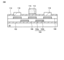
- FIG. 1 is a schematic end view of a transistor according to an embodiment of the present invention.
- FIG. 1 is a schematic top view of a partial configuration of a transistor according to an embodiment of the present invention.
- FIG. 1 is a schematic top view of a partial configuration of a transistor according to an embodiment of the present invention.
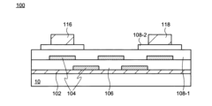
- FIG. 1 is a schematic end view of a transistor according to an embodiment of the present invention.
- FIG. 1 is a schematic end view of a transistor according to an embodiment of the present invention.
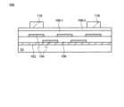
- FIG. 1 is a schematic end view of a transistor according to an embodiment of the present invention.
- FIG. 1 is a schematic end view of a transistor according to an embodiment of the present invention.
- FIG. 1 is a schematic end view of a transistor according to an embodiment of the present invention.
- FIG. 1 is a schematic end view of a transistor according to an embodiment of the present invention.
- FIG. 1 is a schematic end view of a transistor according to an embodiment of the present invention.
- FIG. 1 is a schematic end view of a transistor according to an embodiment of the present invention.
- FIG. 1 is a schematic end view of a transistor according to an embodiment of the present invention.
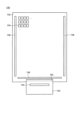
- FIG. 1 is a schematic top view of a display device according to an embodiment of the present invention.
- FIG. 1 is a schematic end view of a display device according to an embodiment of the present invention.
- the term "on top” is used, unless otherwise specified, to include both a case in which another structure is placed directly on top of a structure so as to be in contact with the structure, and a case in which another structure is placed above a structure via yet another structure.
- a structure exposed from another structure refers to a configuration in which a portion of a structure is not covered by another structure, and includes a configuration in which the portion not covered by the other structure is covered by yet another structure.
- the configuration expressed by this expression also includes a configuration in which a structure is not in contact with the other structure.
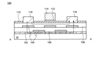
- FIGS 1 and 2A show an example of the structure of a transistor 100 according to an embodiment of the present invention.
- Figures 1 and 2A are a schematic perspective view and a top view, respectively, of the transistor 100
- Figure 2B is a schematic view of an end surface taken along the dashed line A-A' in Figure 2A.
- the transistor 100 is a type of high electron mobility field effect transistor (HEMT).
- HEMT high electron mobility field effect transistor
- the transistor 100 is provided on a substrate 10, and includes a first alignment control film 102, a second alignment control film 106 on the first alignment control film 102, a plurality of blocking films 104 on the first alignment control film 102, an active layer (also called an electron transit layer) 108 on the second alignment control film 106 and the blocking film 104, an electron supply layer 110 on the active layer 108, and a pair of terminals (a first terminal 116 and a second terminal 118) located on the active layer 108 and electrically connected to the active layer 108 and the electron supply layer 110.
- the first terminal 116 and the second terminal 118 may be in contact with the active layer 108, or may be in contact with the active layer 108 via the electron supply layer 110 (not shown).
- the transistor 100 further includes a gate electrode 114 that is in direct contact with the electron supply layer 110 or is provided on the electron supply layer 110 via a gate insulating film 112 of any configuration. These configurations will be described below.
- Substrate 10 supports the transistor 100. Therefore, any substrate can be used as the substrate 10 as long as it has a configuration that can realize this function.
- a single crystal silicon substrate, a sapphire substrate, a quartz substrate, or an amorphous glass substrate can be used as the substrate 10.
- a resin substrate such as a polyimide substrate, a polyamide substrate, a polycarbonate substrate, an acrylic resin substrate, a polysiloxane substrate, or a fluororesin substrate may be used as the substrate 10.
- the substrate 10 may be flexible. As described later, in the manufacture of the transistor 100, the high temperature required for epitaxial growth of an inorganic semiconductor is not necessarily required.
- the substrate 10 preferably has a thermal expansion coefficient smaller than 50 ⁇ 10 ⁇ 7 /° C. and a strain point of 600° C. or higher.
- the content of alkali metals such as sodium in the substrate 10 is preferably 0.1% or less.
- a glass substrate formed of aluminoborosilicate glass or aluminosilicate glass can be used.
- an undercoat may be provided on the substrate 10 to prevent the diffusion of impurities such as alkali metal ions.
- the undercoat is formed, for example, by a sputtering method or a chemical vapor deposition (CVD) method, and is a laminate of one or more films containing silicon-containing inorganic compounds such as silicon oxide and silicon nitride.
- the first orientation control film 102 is provided on the substrate 10.
- the first orientation control film 102 is a film that has a function of controlling the orientation of the active layer 108 and the second orientation control film 106 provided thereon to promote crystallization.
- the first orientation control film 102 can include a conductive material having a hexagonal close-packed structure, a face-centered cubic structure, or a structure equivalent thereto.
- the hexagonal close-packed structure or a structure equivalent to the face-centered cubic structure includes a crystal structure in which the c-axis is not perpendicular to the a-axis and the b-axis.
- the first orientation control film 102 is oriented in the (0001) direction, i.e., the c-axis direction, relative to the substrate 10.
- the first orientation control film 102 having a face-centered cubic structure or a structure equivalent thereto is oriented in the (111) direction relative to the substrate 10. Therefore, the c-axis of the first orientation control film 102 is oriented in a direction perpendicular or approximately perpendicular to the surface on which the first orientation control film 102 is provided (i.e., the surface of the substrate 10).
- the active layer 108 contains a gallium nitride material
- the second orientation control film 106 may also contain a gallium nitride material.
- the gallium nitride material has a hexagonal close-packed structure and grows crystals in the c-axis direction so as to minimize its surface energy. Therefore, by forming the active layer 108 and the second orientation control film 106 on the first orientation control film 102, the crystal growth in the c-axis direction of the second orientation control film 106 and the active layer 108 is promoted. As a result, the crystallinity of the active layer 108 is improved.
- Such a first alignment control film 102 may include a conductive material containing titanium, zinc, aluminum, silver, nickel, or copper. More specifically, the first alignment control film 102 may include inorganic compounds such as titanium nitride, titanium oxide, zinc oxide, and BiLaTiO, and metals such as titanium, aluminum, silver, calcium, nickel, copper, strontium, rhodium, palladium, cerium, ytterbium, iridium, platinum, gold, lead, actinium, and thorium.
- inorganic compounds such as titanium nitride, titanium oxide, zinc oxide, and BiLaTiO
- metals such as titanium, aluminum, silver, calcium, nickel, copper, strontium, rhodium, palladium, cerium, ytterbium, iridium, platinum, gold, lead, actinium, and thorium.
- the first alignment control film 102 may include metal oxides such as BiLaTiO, SrFeO, BiFeO, BaFeO, ZnFeO, and PMnN-PZT, conductive metal borides such as magnesium diboride, and carbon materials such as graphene and graphite.
- metal oxides such as BiLaTiO, SrFeO, BiFeO, BaFeO, ZnFeO, and PMnN-PZT
- conductive metal borides such as magnesium diboride
- carbon materials such as graphene and graphite.
- the first alignment control film 102 may be formed by using a CVD method, a sputtering method, or a deposition method.
- the surface of the first alignment control film 102 is highly flat. Specifically, it is preferable that the arithmetic mean roughness (Ra) of the surface of the first alignment control film 102 is smaller than 2.3 nm. It is also preferable that the root mean square roughness (Rq) of the surface of the first alignment control film 102 is smaller than 2.9 nm.
- the thickness of the first alignment control film 102 is 50 nm or less, and for example, the first alignment control film 102 is formed with a thickness of 10 nm or more and 50 nm or less.
- each blocking film 104 includes an insulating material.
- a silicon-containing inorganic compound such as silicon oxide or silicon nitride can be used.
- lithium niobate, BiLaTiO, SrFeO, SrFeO, BiFeO, BaFeO, ZnFeO, PMnN-PZT, or the like may be used as a material capable of promoting crystal growth in the c-axis direction of the second alignment control film 106 or the active layer 108.
- the blocking film 104 may be formed by using a CVD method or a sputtering method.
- the blocking films 104 may be arranged so that a portion of them contacts the first alignment control film 102, as shown in FIG. 1 or FIG. 2B. Also, as shown in FIG. 2B, the blocking films 104 may be divided and arranged in a plurality of layers. That is, a portion of the blocking films 104 may be arranged in a layer (first layer) located on the substrate 10 or the first alignment control film 102 side, and the remaining blocking films 104 may be arranged in a layer (second layer) located above the first layer. In either layer, the blocking films 104 are arranged in an island shape. At least a portion of the blocking film 104 located in the first layer is exposed from the blocking film 104 located in the second layer.
- the blocking film 104 located in the first layer may or may not overlap the blocking film 104 located in the second layer. In the former case, the entire first alignment control film 102 may be covered with the blocking films 104. Furthermore, the material contained in the blocking film 104 disposed in the first layer and the material contained in the blocking film 104 disposed in the second layer may be the same or different.
- one of the blocking films 104 overlaps with the first terminal 116.
- the other of the blocking films 104 overlaps with the second terminal 118.
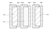
- FIG. 3A which is a schematic top view showing the arrangement of the blocking film 104, the first terminal 116, the second terminal 118, and the gate electrode 114
- the multiple blocking films 104 when any of the blocking films 104 only partially overlaps with the first terminal 116, the second terminal 118, or the gate electrode 114, it is preferable to arrange the multiple blocking films 104 so that the entire bottom surface of the first terminal 116 overlaps with all or at least one of the two or more blocking films 104, and the entire bottom surface of the second terminal 118 overlaps with all or at least one of the other two or more blocking films 104. Similarly, it is preferable to arrange the multiple blocking films 104 so that the entire bottom surface of the gate electrode 114 overlaps with all or at least one of the other two or more blocking films 104.
- multiple blocking films 104 may be arranged so that one of the blocking films 104-1 located in the first layer and one of the blocking films 104-2 located in the second layer partially overlap each other, and the entire bottom surface of the first terminal 116 overlaps both or at least one of these blocking films 104-1 and 104-2 (see FIG. 3B). The same applies to the blocking films 104 that overlap the second terminal 118 and the gate electrode 114.
- the multiple blocking films 104 when viewed from the substrate 10 side, it is preferable to arrange the multiple blocking films 104 so that neither the first terminal 116 nor the second terminal 118 is entirely exposed from the multiple blocking films 104, but is covered by one or more of the multiple blocking films 104.
- the second orientation control film 106 is a film that has the function of controlling the orientation of the active layer 108 provided thereon to promote crystallization in the c-axis direction.
- the second orientation control film 106 also exhibits the function of preventing the formation of a current leakage path. Therefore, the second orientation control film 106 can contain an insulating material having a hexagonal close-packed structure, a face-centered cubic structure, or a structure equivalent thereto.
- the second orientation control film 106 may contain a gallium nitride-based material.
- the gallium nitride-based material include aluminum gallium nitride (AlGaN) and gallium nitride.
- the first orientation control film 102 promotes crystal growth of the second orientation control film 106 in the c-axis direction, improving the crystallinity. As a result, it is possible to promote crystal growth of the active layer 108 provided on the second orientation control film 106 in the c-axis direction.
- the second orientation control film 106 may also be formed using a CVD method, a sputtering method, or the like, depending on the material contained therein.
- the multiple blocking films 104 can be arranged so as to be distributed in two layers. In this case, a portion of the multiple blocking films 104 is provided on the first alignment control film 102, and then the second alignment control film 106 is formed, and then another portion of the multiple blocking films 104 is formed on the second alignment control film 106.
- the active layer 108 and the electron supply layer 110 are, for example, films containing undoped gallium nitride and n-type aluminum gallium nitride, respectively.
- the active layer 108 and the electron supply layer 110 may contain undoped gallium arsenide (GaAs) and n-type aluminum gallium arsenide (AlGaAs), respectively.
- the active layer 108 and the electron supply layer 110 can be provided on the second orientation control film 106 and the blocking film 104 by using a sputtering method.
- the active layer 108 and the electron supply layer 110 can be formed even if an amorphous glass substrate is used as the substrate 10. Furthermore, the crystallization in the c-axis direction of the active layer 108 and the electron supply layer 110 is promoted by the second orientation control film 106 that acts as a base for them. This crystallization promotion function can also be obtained by using a material that promotes crystallization in the c-axis direction for the blocking film 104. Therefore, even if the active layer 108 and the electron supply layer 110 are formed by using a sputtering method, it is possible to achieve a high c-axis orientation.
- the first terminal 116, the second terminal 118, and the gate electrode 114 contain a metal such as aluminum, gold, silver, tantalum, molybdenum, titanium, or copper, or an alloy containing one or more of the above metals.
- the gate insulating film 112, which is an arbitrary configuration, contains, for example, a silicon-containing inorganic compound such as silicon oxide or silicon nitride, or a so-called high-k material such as hafnium silicate, zirconium silicate, hafnium oxide, or zirconium oxide.
- the first terminal 116, the second terminal 118, the gate insulating film 112, and the gate electrode 114 can be efficiently formed by using a sputtering method or an electron beam deposition method, which have a high film formation rate.
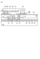
- the transistor 100 is provided with a plurality of blocking films 104. Also, when viewed from the substrate 10 side, the first terminal 116 and the second terminal 118 are not entirely exposed from the plurality of blocking films 104, but can be covered by one or more blocking films 104. Therefore, even if crystal defects or pinholes are formed in the active layer 108, the electron supply layer 110, or the second alignment control film 106, the current leakage path proceeding vertically from the first terminal 116 and the second terminal 118 to the first alignment control film 102 is blocked by the insulating blocking film 104. As a result, as shown by the dotted arrow in FIG. 2B, the current selectively flows through the active layer 108, and the transistor 100 can operate normally. This contributes to providing a highly reliable transistor with excellent characteristics such as high voltage resistance and low on-resistance.
- the structure of the transistor 100 is not limited to the above-mentioned structure.
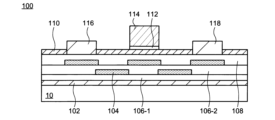
- the plurality of blocking films 104 may not contact the first alignment film 102 and may be separated from the first alignment film 102.
- a portion (106-1) of the second alignment film 106 may be formed on the first alignment film 102, and then a portion of the plurality of blocking films 104 may be formed, and then another portion (106-2) of the second alignment film 106, another portion of the plurality of blocking films 104, and the active layer 108 may be formed in sequence.
- the second alignment film 106 may be provided on the first alignment film 102, and then a portion of the plurality of blocking films 104 may be formed, and then a portion of the active layer 108, another portion of the plurality of blocking films 104, and another portion of the active layer 108 may be formed in sequence.
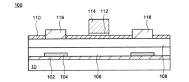
- the transistor 100 may be configured so that all of the blocking films 104 are disposed in the same layer.
- all of the blocking films 104 may be disposed on the second alignment film 106, which may then be covered with the active layer 108.
- all of the blocking films 104 may be formed to contact the first alignment film 102, and the second alignment film 106 and the active layer 108 may be sequentially formed on top of the first alignment film 102.
- the transistor 100 may also be configured so that none of the blocking films 104 overlaps the gate electrode 114 (FIG. 4C).
- the transistor 100 may be configured so as not to include the second alignment control film 106.
- all of the multiple blocking films 104 may be formed on the first alignment control film 102 so as to be in contact with the first alignment control film 102, and an active layer 108 may be provided thereon in direct contact with the first alignment control film 102 and the multiple blocking films 104. Since the process of forming the second alignment control film 106 is not necessary, the manufacturing cost of the transistor 100 may be reduced.
- all or part of the multiple blocking films 104 may be formed to have a two-layer structure.
- the two-layer structure may be composed of a first insulating film 104a and a second insulating film 104b provided thereon.
- the first insulating film 104a may be configured to include a material that can be used in a blocking film 104 having a single layer structure, that is, an insulating material such as the silicon-containing inorganic compound described above.
- the second insulating film 104b may be configured to include an insulating material that can promote the c-axis orientation of the second alignment control film 106 and the active layer 108 formed on the blocking film 104.
- the second insulating film 104b may include a material that can be used in the second alignment control film 106, such as an aluminum-containing insulating compound such as aluminum oxide or aluminum nitride.
- the transistor 100 may be a so-called metal-insulator-semiconductor field-effect transistor (MISFET). That is, as shown in FIG. 6, the active layer 108 may be formed by a stack of a first active layer 108-1 including a p-type gallium nitride layer and a second active layer 108-2 located on the first active layer 108-1 and including an i-type or n-type gallium nitride layer, without providing the electron supply layer 110.
- MISFET metal-insulator-semiconductor field-effect transistor
- the second active layer 108-2 may be provided in a divided manner between the first active layer 108-1 and the first terminal 116, and between the first active layer 108-1 and the second terminal 118, so as to form a source region and a drain region on the first active layer 108-1, respectively.
- the transistors 100 in the above examples are all top-gate transistors, but the transistors 100 may be bottom-gate transistors.
- the first alignment control film 102 is conductive, so that the first alignment control film 102 can function as a gate electrode by connecting wiring (not shown) to supply a gate voltage to the first alignment control film 102. Therefore, as shown in Figures 7A and 7B, there is no need to place a gate electrode 114 on the active layer 108.
- the active layer 108 may be configured as a single layer containing i-type, n-type, or p-type gallium nitride, or may be configured as a stacked structure of a first active layer 108-1 containing i-type or p-type gallium nitride and a second active layer 108-2 containing n-type gallium nitride, as shown in Figures 7A and 7B.
- the second active layer 108-2 may be continuous from the first terminal 116 to the second terminal 118 (FIG. 7B), or the second active layer 108-2 may be provided independently between the first terminal 116 and the first active layer 108-1 and between the second terminal 118 and the first active layer 108-1.
- the transistor 100 according to one embodiment of the present invention is provided with a plurality of blocking films 104. Therefore, even if crystal defects or pinholes occur in the active layer 108, the first alignment film 102, or the second alignment film 106 when forming the first terminal 116, the second terminal 118, and the gate electrode 114, the path of leakage current through the first alignment film 102 caused by the crystal defects or pinholes is blocked. Therefore, by applying this embodiment, it is possible to provide a highly reliable transistor that has high voltage resistance and low on-resistance.
- Second Embodiment an electronic device including the transistor 100 described in the first embodiment will be described. Descriptions of configurations that are the same as or similar to the configuration described in the first embodiment may be omitted.
- the transistor 100 there are no restrictions on the electronic device in which the transistor 100 can be installed, and examples of such electronic devices include power devices that require high current and high voltage, such as motor inverter circuits, power factor correction circuits (PFC), and LLC resonant converters.
- the transistor 100 may be installed in electronic devices such as a switching element for lighting that uses an inorganic light-emitting diode (LED) as a light source, or a switching element for a display device equipped with a display element.
- a display device 130 will be described as an example of an electronic device according to an embodiment of the present invention.
- the display device 130 has a substrate 132 corresponding to the substrate 10, on which a plurality of pixels 134 are arranged in a matrix. Although details will be described later, a display element is provided in each pixel 134.
- the minimum area region that includes all the pixels 134 and the region surrounding it are defined as the display region and the peripheral region, respectively.
- a driving circuit scanning line driving circuit 136, signal line driving circuit 138 for controlling the pixels 134 is provided in the peripheral region. Wiring (not shown) extends from the driving circuit toward the end of the substrate 132 to form a terminal 140.
- the terminal 140 is connected to a flexible wiring board (FPC) 142, and power and video signals supplied from an external circuit (not shown) are supplied to the driving circuit via the FPC 142.
- the driving circuit generates various signals based on the video signals and supplies them to the pixel circuits provided in each pixel 134. This controls the pixels 134, allowing an image to be displayed on the display region.
- a driver IC 144 configured as an integrated circuit formed on a semiconductor substrate may be mounted on the FPC 142.
- FIG. 9 shows a schematic end view of a pixel 134.
- the pixel circuit of each pixel 134 is composed of an appropriate combination of one or more transistors and one or more capacitive elements.
- each pixel 134 of the display device 130 has one or more transistors 100 described in the first embodiment arranged therein.
- the transistor 100 may be provided on an undercoat 146 composed of one or more films containing a silicon-containing inorganic compound or the like, or may be provided directly on the substrate 132.
- the first alignment control film 102 contacts the undercoat 146, and in the latter case, it contacts the substrate 132.
- a planarization film 150 containing a resin such as polyimide, acrylic resin, epoxy resin, or silicone resin is provided on the transistor 100, and a pixel electrode 152 and a common electrode 154 are provided on the planarization film 150.
- a protective insulating film 156 is provided on the pixel electrode 152 and the common electrode 154 to protect their ends.
- the protective insulating film 156 has an opening that exposes the pixel electrode 152 and the common electrode 154.
- the pixel electrode 152 is electrically connected to one terminal of the transistor 100 (e.g., the second terminal 118) through the opening provided in the planarization film 150. This electrically connects the display element 160 to the transistor 100.
- the display element 160 may be appropriately selected from a liquid crystal element, an organic electroluminescent element, an inorganic electroluminescent element, and the like.
- FIG. 9 shows an example in which the display element 160 is an LED.
- the LED may include, for example, a laminate of an n-type cladding layer 166, a light-emitting layer 168, and a p-type cladding layer 170, and a cathode 164 and an anode 162 connected to the n-type cladding layer 166 and the p-type cladding layer 170, respectively.
- the n-type cladding layer 166 and the p-type cladding layer 170 may contain a compound containing a group 13 element and a group 15 element.
- compounds containing a group 13 element and a group 15 element include semiconductors containing aluminum, gallium, and/or indium, as well as nitrogen, phosphorus, and/or arsenic. Typically, gallium-based materials are used.
- Examples include gallium nitride-based materials such as gallium nitride, aluminum gallium nitride, and indium gallium nitride (InGaN), and gallium phosphide-based materials such as gallium phosphide (GaP) and aluminum indium gallium phosphide (AlGaInP).
- the n-type cladding layer 166 and the p-type cladding layer 170 further contain a dopant. Examples of dopants include elements such as silicon, germanium, magnesium, zinc, cadmium, and beryllium.
- the light-emitting layer 168 may be, for example, a single-layer structure of indium gallium nitride, or may have a quantum well structure.
- a quantum well structure is a structure in which multiple thin films with different bandgaps and thicknesses of about 1 nm to 5 nm are alternately stacked, such as an alternating stack of indium gallium nitride and gallium nitride, an alternating stack of indium gallium arsenide phosphide (GaInAsP) and indium phosphide (InP), and an alternating stack of aluminum indium arsenide (AlInAs) and indium gallium arsenide (InGaAs).
- the anode 162 may be, for example, a thin film of a metal such as palladium or gold, or an alloy thereof.
- the cathode 164 may be a metal such as silver or indium, or an alloy thereof.
- the cathode 164 and the anode 162 are connected to the pixel electrode 152 and the common electrode 154, respectively, by bumps 158 containing a conductive adhesive such as solder.
- a protective film composed of one or more films containing an inorganic compound and/or an organic compound such as a polymer may be provided on the display element 160.
- the transistor 100 As described above, in the transistor 100, leakage current caused by damage during film formation of the first terminal 116, the second terminal 118, the gate electrode 114, etc. is effectively suppressed. As a result, the transistor 100 has a high breakdown voltage and a low on-resistance. Therefore, by implementing one of the embodiments of the present invention, it is possible to provide a display device that has low power consumption and is capable of displaying high-brightness images.
- a display device may be combined as appropriate by a person skilled in the art to add or remove components or modify the design, or to add or omit processes or modify conditions, and this is also within the scope of the present invention as long as it contains the gist of the present invention.
Landscapes
- Physics & Mathematics (AREA)
- Optics & Photonics (AREA)
- Engineering & Computer Science (AREA)
- Microelectronics & Electronic Packaging (AREA)
- Thin Film Transistor (AREA)
Abstract
トランジスタは、第1の配向制御膜、第1の配向制御膜上に位置し、絶縁性材料を含む複数のブロッキング膜、複数のブロッキング膜上に位置し、窒化ガリウム系化合物を含む活性層、および活性層上の第1の端子と第2の端子を備える。第1の端子の底面の全体は複数のブロッキング膜の一つと重なり、第2の端子の底面の全体は複数のブロッキング膜の他の一つと重なる。
Description
本発明の実施形態の一つは、トランジスタ、および当該トランジスタを備える電子デバイスに関する。例えば、本発明の実施形態の一つは、窒化ガリウム系化合物を含むトランジスタ、およびこのトランジスタを備える電子デバイスに関する。
近年、窒化ガリウム(GaN)や窒化インジウム(InN)などの13族元素の窒化物を含む半導体素子の開発が精力的に行われている。半導体素子の代表例であるトランジスタに13族元素窒化物を含む半導体を用いることで、高い耐圧性と低いオン抵抗を備える半導体デバイスを作製することができる。例えば特許文献1では、13族元素を活性層に含むトランジスタがガラス基板上に形成できることが開示されている。特許文献2では、酸化ガリウム(Ga2O3)を含む絶縁膜上に13族元素の窒化物を成長させることで、欠陥密度が低い13族元素の半導体膜を形成できることが開示されている。
本発明の実施形態の一つは、新規な構造を有するトランジスタ、およびこのトランジスタを備える電子デバイスを提供することを課題の一つとする。あるいは、本発明の実施形態の一つは、13族元素を含む高信頼性トランジスタ、およびこのトランジスタを備える電子デバイスを提供することを課題の一つとする。
本発明の実施形態の一つは、トランジスタである。このトランジスタは、第1の配向制御膜、第1の配向制御膜上に位置し、絶縁性材料を含む複数のブロッキング膜、複数のブロッキング膜上に位置し、窒化ガリウム系化合物を含む活性層、および活性層上の第1の端子と第2の端子を備える。第1の端子の底面の全体は複数のブロッキング膜の一つと重なり、第2の端子の底面の全体は複数のブロッキング膜の他の一つと重なる。
本発明の実施形態の一つは、表示装置である。この表示装置は、基板、および基板上の複数の画素を備える。複数の画素の少なくとも一つは、トランジスタ、およびトランジスタに電気的に接続される表示素子を備える。トランジスタは、第1の配向制御膜、第1の配向制御膜上に位置し、絶縁性材料を含む複数のブロッキング膜、複数のブロッキング膜上に位置し、窒化ガリウム系化合物を含む活性層、および活性層上の第1の端子と第2の端子を備える。第1の端子の底面の全体は複数のブロッキング膜の一つと重なり、第2の端子の底面の全体は複数のブロッキング膜の他の一つと重なる。
以下、本発明の各実施形態について、図面などを参照しつつ説明する。ただし、本発明は、その要旨を逸脱しない範囲において様々な態様で実施することができ、以下に例示する実施形態の記載内容に限定して解釈されるものではない。
図面は、説明をより明確にするため、実際の態様に比べ、各部の幅、厚さ、形状などについて模式的に表される場合があるが、あくまで一例であって、本発明の解釈を限定するものではない。本明細書と各図において、既出の図に関して説明したものと同様の機能を備えた要素には、同一の符号を付して、重複する説明を省略することがある。同一、あるいは類似する複数の構造を総じて表す際にはこの符号が用いられ、これらを個々に表す際には符号の後にハイフンと自然数が加えられる。
本明細書および請求項において、ある構造体の上に他の構造体を配置する態様を表現するにあたり、単に「上に」と表記する場合、特に断りのない限りは、ある構造体に接するように、直上に他の構造体を配置する場合と、ある構造体の上方に、さらに別の構造体を介して他の構造体を配置する場合との両方を含むものとする。
本明細書および請求項において、「ある構造体が他の構造体から露出する」という表現は、ある構造体の一部が他の構造体によって覆われていない態様を意味し、この他の構造体によって覆われていない部分は、さらに別の構造体によって覆われる態様も含む。また、この表現で表される態様は、ある構造体が他の構造体と接していない態様も含む。
<第1実施形態>
本実施形態では、本発明の実施形態の一つであるトランジスタについて説明する。
本実施形態では、本発明の実施形態の一つであるトランジスタについて説明する。
1.構造
本発明の実施形態の一つであるトランジスタ100の構造の一例を図1、図2A、図2Bに示す。図1と図2Aは、それぞれトランジスタ100の模式的斜視図と上面図であり、図2Bは図2Aの鎖線A-A´に沿った端面の模式図である。これらの図から理解されるように、トランジスタ100は高電子移動度電界効果型トランジスタ(HEMT)の一つである。トランジスタ100は基板10上に設けられ、第1の配向制御膜102、第1の配向制御膜102上の第2の配向制御膜106、第1の配向制御膜102上の複数のブロッキング膜104、第2の配向制御膜106とブロッキング膜104上の活性層(電子走行層とも呼ばれる。)108、活性層108上の電子供給層110、および活性層108上に位置し、活性層108および電子供給層110に電気的に接続される一対の端子(第1の端子116と第2の端子118)を備える。第1の端子116と第2の端子118は、活性層108と接してもよく、図示しないが、電子供給層110を介して活性層108と接してもよい。トランジスタ100はさらに、電子供給層110と直接接する、または任意の構成であるゲート絶縁膜112を介して電子供給層110上に設けられるゲート電極114を備える。以下、これらの構成について説明する。
本発明の実施形態の一つであるトランジスタ100の構造の一例を図1、図2A、図2Bに示す。図1と図2Aは、それぞれトランジスタ100の模式的斜視図と上面図であり、図2Bは図2Aの鎖線A-A´に沿った端面の模式図である。これらの図から理解されるように、トランジスタ100は高電子移動度電界効果型トランジスタ(HEMT)の一つである。トランジスタ100は基板10上に設けられ、第1の配向制御膜102、第1の配向制御膜102上の第2の配向制御膜106、第1の配向制御膜102上の複数のブロッキング膜104、第2の配向制御膜106とブロッキング膜104上の活性層(電子走行層とも呼ばれる。)108、活性層108上の電子供給層110、および活性層108上に位置し、活性層108および電子供給層110に電気的に接続される一対の端子(第1の端子116と第2の端子118)を備える。第1の端子116と第2の端子118は、活性層108と接してもよく、図示しないが、電子供給層110を介して活性層108と接してもよい。トランジスタ100はさらに、電子供給層110と直接接する、または任意の構成であるゲート絶縁膜112を介して電子供給層110上に設けられるゲート電極114を備える。以下、これらの構成について説明する。
(1)基板
基板10はトランジスタ100を支持する。このため、この機能を発現できる構成であれば、任意の基板を基板10として用いることができる。例えば、単結晶シリコン基板やサファイア基板、石英基板の他、非晶質ガラス基板を基板10として用いることができる。あるいは、ポリイミド基板、ポリアミド基板、ポリカーボネート基板、アクリル樹脂基板、ポリシロキサン基板、またはフッ素樹脂基板などの樹脂基板を基板10として用いてもよい。基板10は可撓性を有していてもよい。後述するように、トランジスタ100の作製においては、無機半導体をエピタキシャル成長させる際に必要な高温は必ずしも必要ではない。このため、マザーガラスとも呼ばれる大型の非晶質ガラス基板を基板10として利用することも可能である。このことは、トランジスタ100の製造コストの低減に寄与する。好ましくは、熱膨張係数が低く、歪み点が高く、表面の平坦性が高い基板を基板10として用いる。例えば、基板10は、熱膨張係数が50×10-7/℃より小さく、歪み点が600℃以上であることが好ましい。また、基板10中のナトリウムなどのアルカリ金属の含有量は0.1%以下であることが好ましい。このため、基板10が非晶質ガラス基板である場合、例えば、アルミノホウケイ酸ガラス、アルミノシリケートガラスで形成されるガラス基板を用いることができる。
基板10はトランジスタ100を支持する。このため、この機能を発現できる構成であれば、任意の基板を基板10として用いることができる。例えば、単結晶シリコン基板やサファイア基板、石英基板の他、非晶質ガラス基板を基板10として用いることができる。あるいは、ポリイミド基板、ポリアミド基板、ポリカーボネート基板、アクリル樹脂基板、ポリシロキサン基板、またはフッ素樹脂基板などの樹脂基板を基板10として用いてもよい。基板10は可撓性を有していてもよい。後述するように、トランジスタ100の作製においては、無機半導体をエピタキシャル成長させる際に必要な高温は必ずしも必要ではない。このため、マザーガラスとも呼ばれる大型の非晶質ガラス基板を基板10として利用することも可能である。このことは、トランジスタ100の製造コストの低減に寄与する。好ましくは、熱膨張係数が低く、歪み点が高く、表面の平坦性が高い基板を基板10として用いる。例えば、基板10は、熱膨張係数が50×10-7/℃より小さく、歪み点が600℃以上であることが好ましい。また、基板10中のナトリウムなどのアルカリ金属の含有量は0.1%以下であることが好ましい。このため、基板10が非晶質ガラス基板である場合、例えば、アルミノホウケイ酸ガラス、アルミノシリケートガラスで形成されるガラス基板を用いることができる。
図示しないが、基板10上には、アルカリ金属イオンなどの不純物の拡散を防ぐためのアンダーコートを設けてもよい。アンダーコートは、例えばスパッタリング法または化学気相堆積(CVD)法で形成され、酸化ケイ素や窒化ケイ素などのケイ素含有無機化合物を含む一つまたは複数の膜の積層体である。
(2)第1の配向制御膜
第1の配向制御膜102は、基板10の上に設けられる。第1の配向制御膜102は、その上に設けられる活性層108や第2の配向制御膜106の配向を制御して結晶化を促進する機能を有する膜である。第1の配向制御膜102は、六方最密構造、面心立方構造、またはこれらに準ずる構造を有する導電性材料を含むことができる。ここで、六方最密構造または面心立方構造に準ずる構造とは、a軸およびb軸に対してc軸が直交しない結晶構造を含む。したがって、この構造では、第1の配向制御膜102は、基板10に対して(0001)方向、すなわち、c軸方向に配向する。また、面心立方構造またはそれに準ずる構造を有する第1の配向制御膜102は、基板10に対して(111)方向に配向する。このため、第1の配向制御膜102のc軸は、第1の配向制御膜102が設けられる面(すなわち、基板10の表面)に対して垂直または略垂直な方向に配向する。後述するように、活性層108は窒化ガリウム系材料を含み、第2の配向制御膜106も窒化ガリウム系材料を含むことができるが、窒化ガリウム系材料は六方最密構造を取り、その表面エネルギーを最小化するようにc軸方向に結晶成長することが知られている。このため、第1の配向制御膜102上に活性層108や第2の配向制御膜106を形成することで、第2の配向制御膜106や活性層108のc軸方向への結晶成長が促進される。その結果、活性層108の結晶性が向上する。
第1の配向制御膜102は、基板10の上に設けられる。第1の配向制御膜102は、その上に設けられる活性層108や第2の配向制御膜106の配向を制御して結晶化を促進する機能を有する膜である。第1の配向制御膜102は、六方最密構造、面心立方構造、またはこれらに準ずる構造を有する導電性材料を含むことができる。ここで、六方最密構造または面心立方構造に準ずる構造とは、a軸およびb軸に対してc軸が直交しない結晶構造を含む。したがって、この構造では、第1の配向制御膜102は、基板10に対して(0001)方向、すなわち、c軸方向に配向する。また、面心立方構造またはそれに準ずる構造を有する第1の配向制御膜102は、基板10に対して(111)方向に配向する。このため、第1の配向制御膜102のc軸は、第1の配向制御膜102が設けられる面(すなわち、基板10の表面)に対して垂直または略垂直な方向に配向する。後述するように、活性層108は窒化ガリウム系材料を含み、第2の配向制御膜106も窒化ガリウム系材料を含むことができるが、窒化ガリウム系材料は六方最密構造を取り、その表面エネルギーを最小化するようにc軸方向に結晶成長することが知られている。このため、第1の配向制御膜102上に活性層108や第2の配向制御膜106を形成することで、第2の配向制御膜106や活性層108のc軸方向への結晶成長が促進される。その結果、活性層108の結晶性が向上する。
このような第1の配向制御膜102は、チタン、亜鉛、アルミニウム、銀、ニッケル、または銅を含有する導電性材料を含むことができる。より具体的には、第1の配向制御膜102は、窒化チタン、酸化チタン、酸化亜鉛、BiLaTiOなどの無機化合物や、チタン、アルミニウム、銀、カルシウム、ニッケル、銅、ストロンチウム、ロジウム、パラジウム、セリウム、イッテルビウム、イリジウム、白金、金、鉛、アクチニウム、トリウムなどの金属を含むことができる。これらの材料のほか、第1の配向制御膜102は、BiLaTiO、SrFeO、BiFeO、BaFeO、ZnFeO、PMnN-PZTなどの金属酸化物、二ホウ化マグネシウムなどの導電性を有する金属ホウ化物、グラフェンやグラファイトなどの炭素材料を含んでもよい。
第1の配向制御膜102は、CVD法やスパッタリング法、蒸着法を利用して形成すればよい。なお、より効果的に第2の配向制御膜106や活性層108をc軸方向に結晶成長させるため、第1の配向制御膜102の表面の平坦性が高いことが好ましい。具体的には、第1の配向制御膜102の表面の算術平均粗さ(Ra)は、2.3nmよりも小さいことが好ましい。また、第1の配向制御膜102の表面の二乗平均平方根粗さ(Rq)は、2.9nmよりも小さいことが好ましい。表面の高い平坦性を得るため、第1の配向制御膜102の厚さは50nm以下であることが好ましく、例えば10nm以上50nm以下の厚さで第1の配向制御膜102が形成される。
(3)ブロッキング膜
後述するように、ブロッキング膜104は、第1の端子116と第2の端子118間で活性層108に電流が流れる際、電流パスを活性層108に限定し、電流が第1の配向制御膜102を介してリークする経路(図2Bの鎖線参照。)の形成を防止するために設けられる。このため、各ブロッキング膜104は、絶縁性材料を含む。絶縁性材料としては、酸化ケイ素や窒化ケイ素などのケイ素含有無機化合物を用いることができる。あるいは、第2の配向制御膜106や活性層108のc軸方向への結晶成長を促進可能な材料として、酸化アルミニウムや窒化アルミニウムなどのアルミニウム含有絶縁性化合物の他、ニオブ酸リチウム、BiLaTiO、SrFeO、SrFeO、BiFeO、BaFeO、ZnFeO、PMnN-PZTなどを用いてもよい。ブロッキング膜104は、CVD法やスパッタリング法を用いて形成すればよい。
後述するように、ブロッキング膜104は、第1の端子116と第2の端子118間で活性層108に電流が流れる際、電流パスを活性層108に限定し、電流が第1の配向制御膜102を介してリークする経路(図2Bの鎖線参照。)の形成を防止するために設けられる。このため、各ブロッキング膜104は、絶縁性材料を含む。絶縁性材料としては、酸化ケイ素や窒化ケイ素などのケイ素含有無機化合物を用いることができる。あるいは、第2の配向制御膜106や活性層108のc軸方向への結晶成長を促進可能な材料として、酸化アルミニウムや窒化アルミニウムなどのアルミニウム含有絶縁性化合物の他、ニオブ酸リチウム、BiLaTiO、SrFeO、SrFeO、BiFeO、BaFeO、ZnFeO、PMnN-PZTなどを用いてもよい。ブロッキング膜104は、CVD法やスパッタリング法を用いて形成すればよい。
複数のブロッキング膜104は、図1や図2Bに示すように、一部が第1の配向制御膜102と接するように設けることができる。また、図2Bに示すように、複数のブロッキング膜104は、複数の層に分割して配置してもよい。すなわち、基板10や第1の配向制御膜102側に位置する層(第1の層)に複数のブロッキング膜104の一部を配置し、第1の層の上に位置する層(第2の層)に残りのブロッキング膜104を配置してもよい。いずれの層においても、複数のブロッキング膜104は、島状に配置される。第1の層に位置するブロッキング膜104は、少なくとも一部が第2の層に位置するブロッキング膜104から露出する。第1の層に位置するブロッキング膜104は、第2の層に位置するブロッキング膜104重なってもよく、重ならなくてもよい。前者の場合、第1の配向制御膜102の全体が複数のブロッキング膜104に覆われてもよい。また、第1の層に配置されるブロッキング膜104に含まれる材料と第2の層に配置されるブロッキング膜104に含まれる材料は同一でもよく、異なってもよい。
図1や図2Bから理解されるように、複数のブロッキング膜104の一つは、第1の端子116と重なる。また、複数のブロッキング膜104の他の一つは、第2の端子118と重なる。ここで、ブロッキング膜104、第1の端子116、第2の端子118、ゲート電極114の配置を示す模式的上面図である図3Aに示すように、第1の端子116の底面の全体がブロッキング膜104の一つと重なり、第2の端子118の底面の全体がブロッキング膜104の他の一つと重なるように複数のブロッキング膜104を配置することが好ましい。同様に、ゲート電極114の底面の全体がブロッキング膜104のさらに他の一つと重なるように複数のブロッキング膜104を配置することが好ましい。
あるいは、図3Bに示すように、いずれのブロッキング膜104も第1の端子116、第2の端子118、若しくはゲート電極114と一部しか重ならない場合には、第1の端子116の底面の全体が二つ以上のブロッキング膜104の全てまたは少なくとも一つと重なり、第2の端子118の底面の全体が他の二つ以上のブロッキング膜104の全てまたは少なくとも一方と重なるように複数のブロッキング膜104を配置することが好ましい。同様に、ゲート電極114の底面の全体がさらに他の二つ以上のブロッキング膜104の全てまたは少なくとも一方と重なるように複数のブロッキング膜104を配置することが好ましい。このような配置を実現するためには、例えば、第1の層に位置するブロッキング膜104-1の一つと第2の層に位置するブロッキング膜104-2の一つが互いに一部が重なり合い、かつ、第1の端子116の底面の全体がこれらのブロッキング膜104-1、104-2の両方または少なくとも一方と重なるように複数のブロッキング膜104を配置すればよい(図3B参照。)。第2の端子118とゲート電極114と重なるブロッキング膜104についても同様である。
すなわち、基板10側から見た場合、第1の端子116と第2の端子118の全体がいずれも複数のブロッキング膜104から露出せず、複数のブロッキング膜104のうち一つまたは二つ以上によって覆われるように複数のブロッキング膜104を配置することが好ましい。ゲート電極114についても同様である。後述するように、このような配置を採用することにより、第1の端子116および第2の端子118から第1の配向制御膜102に向かって垂直な方向における電流経路を遮断することができ、その結果、電流リークを防止することができる。
(4)第2の配向制御膜
第2の配向制御膜106は、第1の配向制御膜102と同様、その上に設けられる活性層108の配向を制御してc軸方向への結晶化を促進する機能を有する膜である。また、ブロッキング膜104と同様、第2の配向制御膜106は、電流リーク経路の形成を防止する機能も発現する。したがって、第2の配向制御膜106は、六方最密構造、面心立方構造、またはこれらに準ずる構造を有する絶縁性材料を含むことができる。このような材料としては、酸化アルミニウムや窒化アルミニウムなどのアルミニウム含有絶縁性化合物の他、ニオブ酸リチウム、BiLaTiO、SrFeO、SrFeO、BiFeO、BaFeO、ZnFeO、PMnN-PZTなどが例示される。あるいは、窒化ガリウム系材料を含んでもよい。窒化ガリウム系材料としては、窒化アルミニウムガリウム(AlGaN)や窒化ガリウムなどが挙げられる。上述したように、複数のブロッキング膜104は島状に形成されるため、第2の配向制御膜106は、隣接するブロッキング膜104の間で第1の配向制御膜102と接する。このため、第2の配向制御膜106が窒化ガリウム系材料を含む場合でも、第1の配向制御膜102によって第2の配向制御膜106のc軸方向への結晶成長が促進され、結晶性が向上する。その結果、第2の配向制御膜106上に設けられる活性層108のc軸方向の結晶成長を促進することができる。第2の配向制御膜106も、含まれる材料に応じ、CVD法やスパッタリング法などを用いて形成すればよい。
第2の配向制御膜106は、第1の配向制御膜102と同様、その上に設けられる活性層108の配向を制御してc軸方向への結晶化を促進する機能を有する膜である。また、ブロッキング膜104と同様、第2の配向制御膜106は、電流リーク経路の形成を防止する機能も発現する。したがって、第2の配向制御膜106は、六方最密構造、面心立方構造、またはこれらに準ずる構造を有する絶縁性材料を含むことができる。このような材料としては、酸化アルミニウムや窒化アルミニウムなどのアルミニウム含有絶縁性化合物の他、ニオブ酸リチウム、BiLaTiO、SrFeO、SrFeO、BiFeO、BaFeO、ZnFeO、PMnN-PZTなどが例示される。あるいは、窒化ガリウム系材料を含んでもよい。窒化ガリウム系材料としては、窒化アルミニウムガリウム(AlGaN)や窒化ガリウムなどが挙げられる。上述したように、複数のブロッキング膜104は島状に形成されるため、第2の配向制御膜106は、隣接するブロッキング膜104の間で第1の配向制御膜102と接する。このため、第2の配向制御膜106が窒化ガリウム系材料を含む場合でも、第1の配向制御膜102によって第2の配向制御膜106のc軸方向への結晶成長が促進され、結晶性が向上する。その結果、第2の配向制御膜106上に設けられる活性層108のc軸方向の結晶成長を促進することができる。第2の配向制御膜106も、含まれる材料に応じ、CVD法やスパッタリング法などを用いて形成すればよい。
上述したように、複数のブロッキング膜104は、二つの層に分布するように配置することができる。この場合には、複数のブロッキング膜104の一部を第1の配向制御膜102上に設けた後に第2の配向制御膜106を形成し、その後、複数のブロッキング膜104の他の一部を第2の配向制御膜106上に形成すればよい。
(5)活性層と電子供給層
活性層108と電子供給層110の積層により、トランジスタ100の駆動時にソース/ドレイン電流の経路が形成される(図2Bの点線矢印参照。)。活性層108と電子供給層110は、例えば、それぞれアンドープ窒化ガリウムとn型窒化アルミニウムガリウムを含む膜である。あるいは、活性層108と電子供給層110は、それぞれアンドープヒ化ガリウム(GaAs)とn型ヒ化アルミニウムガリウム(AlGaAs)を含んでもよい。活性層108と電子供給層110は、スパッタリング法を利用して第2の配向制御膜106とブロッキング膜104上に設けることができる。このため、CVD法によるエピタキシャル成長が必要とするような高温での成膜は必ずしも要求されず、非晶質ガラス基板を基板10として用いても活性層108と電子供給層110を形成することができる。また、活性層108と電子供給層110は、その下地として働く第2の配向制御膜106によってc軸方向への結晶化が促進される。この結晶化促進機能は、ブロッキング膜104にc軸方向への結晶化を促進する材料を用いることでも得ることができる。したがって、スパッタリング法を利用して活性層108と電子供給層110を形成しても、高いc軸配向を実現することが可能である。
活性層108と電子供給層110の積層により、トランジスタ100の駆動時にソース/ドレイン電流の経路が形成される(図2Bの点線矢印参照。)。活性層108と電子供給層110は、例えば、それぞれアンドープ窒化ガリウムとn型窒化アルミニウムガリウムを含む膜である。あるいは、活性層108と電子供給層110は、それぞれアンドープヒ化ガリウム(GaAs)とn型ヒ化アルミニウムガリウム(AlGaAs)を含んでもよい。活性層108と電子供給層110は、スパッタリング法を利用して第2の配向制御膜106とブロッキング膜104上に設けることができる。このため、CVD法によるエピタキシャル成長が必要とするような高温での成膜は必ずしも要求されず、非晶質ガラス基板を基板10として用いても活性層108と電子供給層110を形成することができる。また、活性層108と電子供給層110は、その下地として働く第2の配向制御膜106によってc軸方向への結晶化が促進される。この結晶化促進機能は、ブロッキング膜104にc軸方向への結晶化を促進する材料を用いることでも得ることができる。したがって、スパッタリング法を利用して活性層108と電子供給層110を形成しても、高いc軸配向を実現することが可能である。
(6)第1の端子、第2の端子、ゲート絶縁膜、およびゲート電極
第1の端子116、第2の端子118、およびゲート電極114は、アルミニウム、金、銀、タンタル、モリブデン、チタン、銅などの金属、または上記金属を一つまたは複数含む合金を含む。任意の構成であるゲート絶縁膜112は、例えば酸化ケイ素や窒化ケイ素などのケイ素含有無機化合物、あるいはケイ酸ハフニウム、ケイ酸ジルコニウム、酸化ハフニウム、酸化ジルコニウムなどの所謂high-k材料を含む。これらの構成を形成する方法に制約はなく、真空蒸着法や電子ビーム蒸着法、CVD法、スパッタリング法を適宜採用することができる。なかでも、成膜速度の大きなスパッタリング法や電子ビーム蒸着法を用いることで、効率よく第1の端子116、第2の端子118、ゲート絶縁膜112、およびゲート電極114を形成することができる。
第1の端子116、第2の端子118、およびゲート電極114は、アルミニウム、金、銀、タンタル、モリブデン、チタン、銅などの金属、または上記金属を一つまたは複数含む合金を含む。任意の構成であるゲート絶縁膜112は、例えば酸化ケイ素や窒化ケイ素などのケイ素含有無機化合物、あるいはケイ酸ハフニウム、ケイ酸ジルコニウム、酸化ハフニウム、酸化ジルコニウムなどの所謂high-k材料を含む。これらの構成を形成する方法に制約はなく、真空蒸着法や電子ビーム蒸着法、CVD法、スパッタリング法を適宜採用することができる。なかでも、成膜速度の大きなスパッタリング法や電子ビーム蒸着法を用いることで、効率よく第1の端子116、第2の端子118、ゲート絶縁膜112、およびゲート電極114を形成することができる。
しかしながら、スパッタリング法や電子ビーム蒸着法では、ターゲットあるいは蒸着源から飛散する金属原子が活性層108や電子供給層110に高速で衝突するため、これらの層にダメージが生じやすい。その結果、活性層108や電子供給層110、さらにはその下に位置する第2の配向制御膜106にも結晶欠陥やピンホールが形成されることがある。結晶欠陥やピンホールが形成されると、図2Bの鎖線で示す電流リーク経路が形成されるため、トランジスタ100が正常に動作しなくなる。特に第1の端子116、第2の端子118、およびゲート電極114をスパッタリング法や電子ビーム蒸着法で形成する場合、ピンホールに金属元素が入り込むことがあり、電流リークが生じやすい。
しかしながら、上述したように、トランジスタ100には複数のブロッキング膜104が設けられる。また、基板10側から見た場合、第1の端子116と第2の端子118の全体を複数のブロッキング膜104から露出させず、一つまたは二つ以上のブロッキング膜104によって覆うことができる。このため、活性層108や電子供給層110、第2の配向制御膜106に結晶欠陥やピンホールが形成された場合でも、第1の端子116と第2の端子118から第1の配向制御膜102に向かって垂直方向に進む電流リーク経路が絶縁性のブロッキング膜104によって遮断される。その結果、図2Bの点線矢印で示すように、電流は選択的に活性層108を流れ、トランジスタ100が正常動作することができる。このことは、耐圧性が高く、オン抵抗の小さい優れた特性を有する高信頼性トランジスタの提供に寄与する。
2.変形例
トランジスタ100の構造は、上述した構造に限られない。例えば図4Aに示すように、複数のブロッキング膜104はいずれも第1の配向制御膜102と接触せず、第1の配向制御膜102から離隔してもよい。この場合には、第1の配向制御膜102上に第2の配向制御膜106の一部(106-1)を形成した後に複数のブロッキング膜104の一部を形成し、さらに第2の配向制御膜106の他の一部(106-2)、複数のブロッキング膜104の他の一部、および活性層108を順次形成すればよい。あるいは、図示しないが、第1の配向制御膜102上に第2の配向制御膜106を設けた後に複数のブロッキング膜104の一部を形成し、さらに活性層108の一部、複数のブロッキング膜104の他の一部、および活性層108の他の一部を順次形成してもよい。
トランジスタ100の構造は、上述した構造に限られない。例えば図4Aに示すように、複数のブロッキング膜104はいずれも第1の配向制御膜102と接触せず、第1の配向制御膜102から離隔してもよい。この場合には、第1の配向制御膜102上に第2の配向制御膜106の一部(106-1)を形成した後に複数のブロッキング膜104の一部を形成し、さらに第2の配向制御膜106の他の一部(106-2)、複数のブロッキング膜104の他の一部、および活性層108を順次形成すればよい。あるいは、図示しないが、第1の配向制御膜102上に第2の配向制御膜106を設けた後に複数のブロッキング膜104の一部を形成し、さらに活性層108の一部、複数のブロッキング膜104の他の一部、および活性層108の他の一部を順次形成してもよい。
あるいは、複数のブロッキング膜104の全てが同一の層内に配置されるようにトランジスタ100を構成してもよい。例えば、図4Bに示すように、複数のブロッキング膜104の全てを第2の配向制御膜106の上に配置し、これらを活性層108で覆ってもよい。あるいは、図4Cに示すように、複数のブロッキング膜104の全てを第1の配向制御膜102と接するように形成し、その上に第2の配向制御膜106と活性層108を順次設けてもよい。なお、複数のブロッキング膜104のいずれもゲート電極114と重ならないようにトランジスタ100を構成してもよい(図4C)。
あるいは、第2の配向制御膜106を含まないようにトランジスタ100を構成してもよい。具体的には、図5Aに示すように、複数のブロッキング膜104の全てを第1の配向制御膜102と接するように第1の配向制御膜102の上に形成し、その上に、第1の配向制御膜102と複数のブロッキング膜104と直接接する活性層108を設けてもよい。第2の配向制御膜106形成工程が不要になるため、トランジスタ100の製造コストを低減することができる。
あるいは、図5Bに示すように、複数のブロッキング膜104の全てまたは一部を二層構造となるように形成してもよい。二層構造は、第1の絶縁膜104aとその上に設けられる第2の絶縁膜104bで構成すればよい。第1の絶縁膜104aは、単層構造のブロッキング膜104で使用可能な材料、すなわち、上述したケイ素含有無機化合物などの絶縁性材料を含むように構成すればよい。一方、第2の絶縁膜104bは、ブロッキング膜104の上に形成される第2の配向制御膜106や活性層108のc軸配向を促進可能な絶縁性材料を含むように構成すればよい。具体的には、第2の絶縁膜104bは、酸化アルミニウムや窒化アルミニウムなどのアルミニウム含有絶縁性化合物に例示される、第2の配向制御膜106で使用可能な材料を含むことができる。
あるいは、トランジスタ100は、所謂金属絶縁膜電界効果型トランジスタ(MISFET)でもよい。すなわち、図6に示すように、電子供給層110を設けず、p型窒化ガリウム層を含む第1の活性層108-1、第1の活性層108-1上に位置し、i型またはn型窒化ガリウムを含む第2の活性層108-2の積層で活性層108を構成してもよい。第2の活性層108-2は、第1の活性層108-1の上にソース領域とドレイン領域を形成するように、それぞれ第1の活性層108-1と第1の端子116の間、および第1の活性層108-1と第2の端子118の間に分割して設ければよい。
上述した例のトランジスタ100は、いずれもトップゲート型のトランジスタであるが、トランジスタ100はボトムゲート型のトランジスタでもよい。上述したように、第1の配向制御膜102は導電性を有するため、第1の配向制御膜102にゲート電圧を供給するため図示しない配線を接続することで、第1の配向制御膜102をゲート電極として機能させることができる。したがって、図7Aや図7Bに示すように、活性層108上にゲート電極114を配置する必要は無い。活性層108は、i型、n型、またはp型窒化ガリウムを含む単層として構成してもよいが、図7A、図7Bに示すように、i型またはp型窒化ガリウムを含む第1の活性層108-1とn型窒化ガリウムを含む第2の活性層108-2の積層構造として構成してもよい。第2の活性層108-2は、第1の端子116から第2の端子118に亘って連続してもよく(図7B)、第1の端子116と第1の活性層108-1の間と第2の端子118と第1の活性層108-1の間にそれぞれ独立に第2の活性層108-2を設けてもよい。
上述したように、本発明の実施形態の一つに係るトランジスタ100には、複数のブロッキング膜104が設けられる。このため、第1の端子116、第2の端子118、およびゲート電極114を形成する際に活性層108や第1の配向制御膜102、第2の配向制御膜106に結晶欠陥やピンホールが生じても、結晶欠陥やピンホールに起因する第1の配向制御膜102を介したリーク電流の経路が遮断される。このため、本実施形態を適用することで、耐圧性が高く、低いオン抵抗を示す高信頼性トランジスタを提供することができる。
<第2実施形態>
本実施形態では、第1実施形態で述べたトランジスタ100を備える電子デバイスについて説明する。第1実施形態で述べた構成と同様または類似する構成については、説明を割愛することがある。
本実施形態では、第1実施形態で述べたトランジスタ100を備える電子デバイスについて説明する。第1実施形態で述べた構成と同様または類似する構成については、説明を割愛することがある。
トランジスタ100が設けられる電子デバイスに制約はなく、大電流・高電圧が要求されるモータ・インバータ回路、力率改善回路(PFC)、LLC共振コンバータなどのパワーデバイスが挙げられる。あるいは、無機発光ダイオード(LED)を光源とする照明のスイッチング素子、表示素子が搭載された表示装置のスイッチング素子などの電子デバイスにトランジスタ100を搭載してもよい。以下、本発明の実施形態に係る電子デバイスの一例として、表示装置130を説明する。
図8に表示装置130の模式的上面図を示す。図8に示すように、表示装置130は、基板10に対応する基板132を有し、その上に複数の画素134がマトリクス状に設けられる。詳細は後述するが、各画素134には表示素子が設けられる。全ての画素134を包含する最小面積の領域、およびこれを取り囲む領域がそれぞれ表示領域と周辺領域として定義される。周辺領域には画素134を制御するための駆動回路(走査線駆動回路136、信号線駆動回路138)が設けられる。駆動回路からは図示しない配線が基板132の端部に向かって延伸し、端子140を形成する。端子140はフレキシブル配線基板(FPC)142と接続され、図示しない外部回路から供給される電源や映像信号がFPC142を介して駆動回路に供給される。駆動回路は、映像信号に基づいて各種信号を生成し、各画素134に設けられる画素回路に供給する。これにより、画素134が制御され、表示領域上に映像を表示することができる。なお、信号線駆動回路138に替わり、または信号線駆動回路138とともに、半導体基板上に形成される集積回路で構成されるドライバIC144をFPC142上に搭載してもよい。
図9に、画素134の模式的端面図を示す。各画素134の画素回路は、一つまたは複数のトランジスタ、および一つまたは複数の容量素子などを適宜組み合わせて構成される。図9に示すように、表示装置130の各画素134には、第1実施形態で述べたトランジスタ100が一つまたは複数配置される。トランジスタ100は、ケイ素含有無機化合物などを含む一つまたは複数の膜で構成されるアンダーコート146上に設けてもよく、基板132上に直接設けてもよい。前者の場合、第1の配向制御膜102はアンダーコート146と接し、後者の場合には基板132と接する。
トランジスタ100の上には、ポリイミドやアクリル樹脂、エポキシ樹脂、シリコン樹脂などの樹脂を含む平坦化膜150が設けられ、平坦化膜150上には画素電極152と共通電極154が設けられる。画素電極152と共通電極154上には、これらの端部を保護する保護絶縁膜156が設けられる。保護絶縁膜156には、画素電極152と共通電極154を露出する開口が設けられる。画素電極152は、平坦化膜150に設けられる開口を介してトランジスタ100の一方の端子(例えば第2の端子118)と電気的に接続される。これにより、表示素子160がトランジスタ100と電気的に接続される。
表示素子160は、液晶素子、有機電界発光素子、無機電界発光素子などから適宜選択すればよい。図9には、表示素子160がLEDである例が示されている。表示素子160であるLEDの構成に制約はなく、例えば、n型クラッド層166、発光層168、およびp型クラッド層170の積層体、およびn型クラッド層166とp型クラッド層170にそれぞれ接続される陰極164と陽極162を含むことができる。
n型クラッド層166とp型クラッド層170は、第13族元素と第15族元素を含む化合物を含むことができる。第13族元素と第15族元素を含む化合物としては、アルミニウム、ガリウム、および/またはインジウム、ならびに窒素、リン、および/またはヒ素を含む半導体が挙げられる。典型的には、ガリウム系材料が挙げられる。例えば、窒化ガリウム、窒化アルミニウムガリウム、窒化インジウムガリウム(InGaN)などの窒化ガリウム系材料、リン化ガリウム(GaP)、アルミニウムインジウムガリウムリン(AlGaInP)などのリン化ガリウム系材料が例示される。n型クラッド層166とp型クラッド層170にはドーパントがさらに含まれる。ドーパントとしては、ケイ素やゲルマニウム、マグネシウム、亜鉛、カドミウム、ベリリウムなどの元素が挙げられる。
発光層168は、例えば窒化インジウムガリウムの単層構造でもよく、あるいは量子井戸構造を有してもよい。量子井戸構造とは、バンドギャップが異なり、1nmから5nm程度の厚さを有する複数の薄膜を交互に積層した構造であり、例えば窒化インジウムガリウムと窒化ガリウムの交互積層体、ひ化りん化インジウムガリウム(GaInAsP)とリン化インジウム(InP)の交互積層体、ひ化アルミニウムインジウム(AlInAs)とひ化インジウムガリウム(InGaAs)の交互積層体などが例示される。
陽極162としては、例えば、パラジウム、金などの金属、またはこれらの合金の薄膜を用いることができる。陰極164としては、銀またはインジウムなどの金属、またはこれらの合金を用いることができる。陰極164と陽極162は、それぞれはんだなどの導電性接着剤を含むバンプ158によって画素電極152と共通電極154に接続される。
図示しないが、表示素子160上には、無機化合物および/または高分子に例示される有機化合物を含む一つまたは複数の膜で構成される保護膜を設けてもよい。
上述したように、トランジスタ100では、第1の端子116や第2の端子118、ゲート電極114などの成膜時のダメージに起因するリーク電流が効果的に抑制される。このため、トランジスタ100は耐圧が高く、低いオン抵抗を示す。したがって、本発明の実施形態の一つを実施することにより、低い消費電力を示すと同時に、高輝度の映像を表示可能な表示装置を提供することができる。
本発明の実施形態として上述した各実施形態は、相互に矛盾しない限りにおいて、適宜組み合わせて実施することができる。また、各実施形態の表示装置を基にして、当業者が適宜構成要素の追加、削除もしくは設計変更を行ったもの、または、工程の追加、省略もしくは条件変更を行ったものも、本発明の要旨を備えている限り、本発明の範囲に含まれる。
上述した各実施形態の態様によりもたらされる作用効果とは異なる他の作用効果であっても、本明細書の記載から明らかなもの、または、当業者において容易に予測し得るものについては、当然に本発明によりもたらされるものと解される。
10:基板、100:トランジスタ、102:第1の配向制御膜、104:ブロッキング膜、104a:第1の絶縁膜、104b:第2の絶縁膜、106:第2の配向制御膜、108:活性層、108-1:第1の活性層、108-2:第2の活性層、110:電子供給層、112:ゲート絶縁膜、114:ゲート電極、116:第1の端子、118:第2の端子、130:表示装置、132:基板、134:画素、136:走査線駆動回路、138:信号線駆動回路、140:端子、142:FPC、144:ドライバIC、146:アンダーコート、150:平坦化膜、152:画素電極、154:共通電極、156:保護絶縁膜、158:バンプ、160:表示素子、162:陽極、164:陰極、166:n型クラッド層、168:発光層、170:p型クラッド層
Claims (20)
- 第1の配向制御膜、
前記第1の配向制御膜上に位置し、絶縁性材料を含む複数のブロッキング膜、
前記複数のブロッキング膜上に位置し、窒化ガリウム系化合物を含む活性層、および
前記活性層上の第1の端子と第2の端子を備え、
前記第1の端子の底面の全体が前記複数のブロッキング膜の一つと重なり、前記第2の端子の底面の全体が前記複数のブロッキング膜の他の一つと重なる、トランジスタ。 - 前記第1の配向制御膜は導電性であり、チタン、亜鉛、アルミニウム、銀、ニッケル、または銅を含む、請求項1に記載のトランジスタ。
- 前記第1の配向制御膜と前記活性層の間に第2の配向制御膜をさらに備え、
前記第2の配向制御膜は、窒化ガリウム系化合物またはアルミニウム含有絶縁性化合物を含む、請求項1に記載のトランジスタ。 - 前記複数のブロッキング膜は、第1の層、および前記第1の層の上に位置し、前記第1の層から離隔する第2の層に配置され、
前記第1の層に配置される前記ブロッキング膜は、前記第2の配向制御膜に覆われる、請求項3に記載のトランジスタ。 - 前記複数のブロッキング膜の少なくとも一つが前記第1の配向制御膜と接する、請求項1に記載のトランジスタ。
- 前記活性層の上にゲート電極をさらに備える、請求項1に記載のトランジスタ。
- 前記活性層と前記ゲート電極の間に電子供給層をさらに備える、請求項6に記載のトランジスタ。
- 前記ゲート電極と前記電子供給層の間にゲート絶縁膜をさらに備える、請求項7に記載のトランジスタ。
- 前記第1の配向制御膜は、ゲート電圧が供給されるように構成される、請求項1に記載のトランジスタ。
- 前記複数のブロッキング膜は、それぞれ第1の絶縁膜と前記第1の絶縁膜上の第2の絶縁膜を有し、
前記絶縁性材料は、前記第1の絶縁膜に含まれ、
前記第2の絶縁膜は、アルミニウム含有絶縁性化合物を含む、請求項1に記載のトランジスタ。 - 基板、および
前記基板上の複数の画素を備え、
前記複数の画素の少なくとも一つは、トランジスタ、および前記トランジスタに電気的に接続される表示素子を備え、
前記トランジスタは、
第1の配向制御膜、
前記第1の配向制御膜上に位置し、絶縁性材料を含む複数のブロッキング膜、
前記複数のブロッキング膜上に位置し、窒化ガリウム系化合物を含む活性層、および
前記活性層上の第1の端子と第2の端子を備え、
前記第1の端子の底面の全体が前記複数のブロッキング膜の一つと重なり、前記第2の端子の底面の全体が前記複数のブロッキング膜の他の一つと重なる表示装置。 - 前記第1の配向制御膜は、導電性であり、チタン、亜鉛、アルミニウム、銀、ニッケル、または銅を含む、請求項11に記載の表示装置。
- 前記トランジスタは、前記第1の配向制御膜と前記活性層の間に第2の配向制御膜をさらに備え、
前記第2の配向制御膜は、窒化ガリウム系化合物またはアルミニウム含有絶縁性化合物を含む、請求項11に記載の表示装置。 - 前記複数のブロッキング膜は、第1の層、および前記第1の層の上に位置し、前記第1の層から離隔する第2の層に配置され、
前記第1の層に配置された前記ブロッキング膜は、前記第2の配向制御膜に覆われる、請求項13に記載の表示装置。 - 前記複数のブロッキング膜の少なくとも一つが前記第1の配向制御膜と接する、請求項11に記載の表示装置。
- 前記トランジスタは、前記活性層の上にゲート電極をさらに備える、請求項11に記載の表示装置。
- 前記トランジスタは、前記活性層と前記ゲート電極の間に電子供給層をさらに備える、請求項16に記載の表示装置。
- 前記トランジスタは、前記ゲート電極と前記電子供給層の間にゲート絶縁膜をさらに備える、請求項17に記載の表示装置。
- 前記第1の配向制御膜は、ゲート電圧が供給されるように構成される、請求項11に記載の表示装置。
- 前記複数のブロッキング膜は、それぞれ第1の絶縁膜と前記第1の絶縁膜上の第2の絶縁膜を有し、
前記絶縁性材料は、前記第1の絶縁膜に含まれ、
前記第2の絶縁膜は、アルミニウム含有絶縁性化合物を含む、請求項11に記載の表示装置。
Priority Applications (1)
| Application Number | Priority Date | Filing Date | Title |
|---|---|---|---|
| US19/312,399 US20250380445A1 (en) | 2023-03-06 | 2025-08-28 | Transistor and display device including the transistor |
Applications Claiming Priority (2)
| Application Number | Priority Date | Filing Date | Title |
|---|---|---|---|
| JP2023033613 | 2023-03-06 | ||
| JP2023-033613 | 2023-03-06 |
Related Child Applications (1)
| Application Number | Title | Priority Date | Filing Date |
|---|---|---|---|
| US19/312,399 Continuation US20250380445A1 (en) | 2023-03-06 | 2025-08-28 | Transistor and display device including the transistor |
Publications (1)
| Publication Number | Publication Date |
|---|---|
| WO2024185367A1 true WO2024185367A1 (ja) | 2024-09-12 |
Family
ID=92674396
Family Applications (1)
| Application Number | Title | Priority Date | Filing Date |
|---|---|---|---|
| PCT/JP2024/003828 Ceased WO2024185367A1 (ja) | 2023-03-06 | 2024-02-06 | トランジスタ、およびトランジスタを備える表示装置 |
Country Status (2)
| Country | Link |
|---|---|
| US (1) | US20250380445A1 (ja) |
| WO (1) | WO2024185367A1 (ja) |
Cited By (1)
| Publication number | Priority date | Publication date | Assignee | Title |
|---|---|---|---|---|
| CN119730646A (zh) * | 2024-10-29 | 2025-03-28 | 福州大学 | 一种双栅极调控无注入发光器件制备工艺 |
Citations (5)
| Publication number | Priority date | Publication date | Assignee | Title |
|---|---|---|---|---|
| JP2011228428A (ja) * | 2010-04-19 | 2011-11-10 | Toyoda Gosei Co Ltd | Iii族窒化物半導体からなる半導体装置およびその製造方法、電力変換装置 |
| JP2013149974A (ja) * | 2013-01-11 | 2013-08-01 | Fujitsu Ltd | 多結晶SiC基板を有する化合物半導体ウエハ、化合物半導体装置とそれらの製造方法 |
| JP2015065241A (ja) * | 2013-09-24 | 2015-04-09 | ルネサスエレクトロニクス株式会社 | 半導体装置の製造方法および半導体装置 |
| US10530125B1 (en) * | 2018-11-30 | 2020-01-07 | Poet Technologies, Inc. | Vertical cavity surface emitting laser |
| WO2023276575A1 (ja) * | 2021-06-29 | 2023-01-05 | 株式会社ジャパンディスプレイ | 半導体装置 |
-
2024
- 2024-02-06 WO PCT/JP2024/003828 patent/WO2024185367A1/ja not_active Ceased
-
2025
- 2025-08-28 US US19/312,399 patent/US20250380445A1/en active Pending
Patent Citations (5)
| Publication number | Priority date | Publication date | Assignee | Title |
|---|---|---|---|---|
| JP2011228428A (ja) * | 2010-04-19 | 2011-11-10 | Toyoda Gosei Co Ltd | Iii族窒化物半導体からなる半導体装置およびその製造方法、電力変換装置 |
| JP2013149974A (ja) * | 2013-01-11 | 2013-08-01 | Fujitsu Ltd | 多結晶SiC基板を有する化合物半導体ウエハ、化合物半導体装置とそれらの製造方法 |
| JP2015065241A (ja) * | 2013-09-24 | 2015-04-09 | ルネサスエレクトロニクス株式会社 | 半導体装置の製造方法および半導体装置 |
| US10530125B1 (en) * | 2018-11-30 | 2020-01-07 | Poet Technologies, Inc. | Vertical cavity surface emitting laser |
| WO2023276575A1 (ja) * | 2021-06-29 | 2023-01-05 | 株式会社ジャパンディスプレイ | 半導体装置 |
Cited By (1)
| Publication number | Priority date | Publication date | Assignee | Title |
|---|---|---|---|---|
| CN119730646A (zh) * | 2024-10-29 | 2025-03-28 | 福州大学 | 一种双栅极调控无注入发光器件制备工艺 |
Also Published As
| Publication number | Publication date |
|---|---|
| US20250380445A1 (en) | 2025-12-11 |
Similar Documents
| Publication | Publication Date | Title |
|---|---|---|
| US11527520B2 (en) | Micro light emitting diode display device | |
| KR100730082B1 (ko) | 질화물계 반도체 발광소자 | |
| EP3767675B1 (en) | Array substrate and method for manufacturing same, and display device | |
| JP6662464B2 (ja) | 発光素子 | |
| KR102905220B1 (ko) | 표시 장치 및 표시 장치의 제조 방법 | |
| EP3895212B1 (en) | Active matrix led array | |
| US20250380445A1 (en) | Transistor and display device including the transistor | |
| US12610662B2 (en) | Laminated structure | |
| US12283579B2 (en) | Display device with guard ring | |
| JP7807567B2 (ja) | 発光素子および発光素子の製造方法 | |
| EP3855513A2 (en) | Semiconductor led and method of manufacturing the same | |
| US12593550B2 (en) | Display apparatus and manufacturing method thereof | |
| US20250359400A1 (en) | Light-emitting element and display device and lighting device including the light-emitting element | |
| US20250380541A1 (en) | Semiconductor device and manufacturing method thereof | |
| US20240274648A1 (en) | Display device and manufacturing method thereof | |
| US20240379730A1 (en) | Light emitting device | |
| JP7592881B2 (ja) | アモルファス基板上の窒化ガリウム系半導体デバイス | |
| CN221651500U (zh) | 显示装置 | |
| US20250191913A1 (en) | Semiconductor device and method for manufacturing semiconductor device | |
| JP2021118360A (ja) | 半導体発光ダイオード及びその製造方法 | |
| US20260123195A1 (en) | Display device, electronic device, and method for manufacturing the same | |
| US20250220999A1 (en) | Laminated structure, method for manufacturing laminated structure, and semiconductor device | |
| WO2025169644A1 (ja) | 発光素子および発光素子の製造方法 | |
| US20250133892A1 (en) | Display device and manufacturing method thereof | |
| JP7669508B2 (ja) | 発光装置および発光装置形成基板 |
Legal Events
| Date | Code | Title | Description |
|---|---|---|---|
| 121 | Ep: the epo has been informed by wipo that ep was designated in this application |
Ref document number: 24766742 Country of ref document: EP Kind code of ref document: A1 |
|
| NENP | Non-entry into the national phase |
Ref country code: DE |
|
| 122 | Ep: pct application non-entry in european phase |
Ref document number: 24766742 Country of ref document: EP Kind code of ref document: A1 |