WO2024185136A1 - アンテナ装置及び無線装置 - Google Patents
アンテナ装置及び無線装置 Download PDFInfo
- Publication number
- WO2024185136A1 WO2024185136A1 PCT/JP2023/009102 JP2023009102W WO2024185136A1 WO 2024185136 A1 WO2024185136 A1 WO 2024185136A1 JP 2023009102 W JP2023009102 W JP 2023009102W WO 2024185136 A1 WO2024185136 A1 WO 2024185136A1
- Authority
- WO
- WIPO (PCT)
- Prior art keywords
- substrate
- conductor
- antenna device
- antenna
- power supply
- Prior art date
- Legal status (The legal status is an assumption and is not a legal conclusion. Google has not performed a legal analysis and makes no representation as to the accuracy of the status listed.)
- Ceased
Links
Images




Classifications
-
- H—ELECTRICITY
- H01—ELECTRIC ELEMENTS
- H01P—WAVEGUIDES; RESONATORS, LINES, OR OTHER DEVICES OF THE WAVEGUIDE TYPE
- H01P3/00—Waveguides; Transmission lines of the waveguide type
- H01P3/02—Waveguides; Transmission lines of the waveguide type with two longitudinal conductors
- H01P3/08—Microstrips; Strip lines
-
- H—ELECTRICITY
- H01—ELECTRIC ELEMENTS
- H01Q—ANTENNAS, i.e. RADIO AERIALS
- H01Q1/00—Details of, or arrangements associated with, antennas
- H01Q1/42—Housings not intimately mechanically associated with radiating elements, e.g. radome
Definitions
- This disclosure relates to an antenna device and a wireless device.
- EIRP equivalent isotropically radiated power
- Patent Document 1 discloses an antenna structure with a microstrip line.
- a power feed circuit is formed on the front surface of a printed circuit board, and a ground layer is formed on the back surface of the printed circuit board.
- a ground layer is formed on the back surface of the printed circuit board.
- the purpose of this disclosure is to provide an antenna device and a wireless device that enable improved antenna gain at low cost.
- the antenna device comprises a substrate, a plurality of antenna elements arranged on a first surface of the substrate, a power supply circuit arranged on a second surface, which is the reverse surface of the first surface of the substrate, and a first conductor arranged in a position opposite the power supply circuit, and a gap is formed between the power supply circuit and the first conductor.
- the antenna device includes a substrate, a plurality of antenna elements arranged on a first surface of the substrate, a power supply circuit arranged on a second surface of the substrate opposite the first surface, which distributes power to the plurality of antenna elements, and a conductor arranged opposite the power supply circuit and functioning as a ground for the power supply circuit, with an air gap formed between the power supply circuit and the conductor.
- a wireless device in one aspect of the present invention, includes an antenna device and a transceiver, the antenna device including a substrate, a plurality of antenna elements arranged on a first surface of the substrate, a power supply circuit arranged on a second surface of the substrate that is the reverse side of the first surface, and a first conductor arranged in a position opposite the power supply circuit, with a gap formed between the power supply circuit and the first conductor.
- This disclosure makes it possible to provide an antenna device and a wireless device that can improve antenna gain at low cost.
- FIG. 1 is a diagram illustrating a configuration of an antenna device according to a first embodiment.
- 13 is a diagram illustrating a configuration of an antenna device according to a second embodiment.
- FIG. 11 is a cross-sectional view of an antenna device according to a second embodiment.
- 13A and 13B are diagrams illustrating an example of dimensions of an antenna device according to a second embodiment.
- 13 is a diagram illustrating an example of a wireless device having an antenna device according to a second embodiment.
- 13 is a diagram illustrating a configuration of an antenna device according to a first modified example of the second embodiment.
- FIG. 13 is a diagram illustrating a configuration of an antenna device according to a second modified example of the second embodiment.
- FIG. 13 is a diagram illustrating a configuration of an antenna device according to a third embodiment.
- FIG. FIG. 11 is a cross-sectional view of an antenna device according to a third embodiment.
- 13A and 13B are diagrams illustrating a first example of arrangement of a support member in the third embodiment.
- 13A and 13B are diagrams illustrating a second arrangement example of the support member in the third embodiment.
- 13 is a diagram illustrating an example of a wireless device having an antenna device according to a third embodiment.
- FIG. 1 is a diagram showing a configuration of an antenna device 1 according to a first embodiment of the present disclosure.
- the antenna device 1 in this embodiment includes a substrate 10, an antenna element 20, a power supply circuit 30, and a conductor 40.
- Antenna device 1 is a device that performs transmission processing of radio frequency signals.
- An electrical wiring pattern is provided on the substrate 10 of the antenna device 1, and a plurality of antenna elements 20 are arranged on one side, the first side, of the substrate 10.
- the plurality of antenna elements 20 are arranged along the X direction in FIG. 1 (the direction from the back side to the front side of the paper, or the opposite direction).
- the substrate 10 may be referred to as a printed circuit board.
- the antenna element 20 of the antenna device 1 is disposed on a first surface, which is one surface of the substrate 10.
- the antenna element 20 functions as a primary resonator for the transceiver of the antenna device 1 to transmit and receive signals.
- the power supply circuit 30 of the antenna device 1 is disposed on the second surface, which is the reverse side of the first surface of the substrate 10.
- the power supply circuit 30 is a circuit that supplies power to the multiple antenna elements 20.
- the conductor 40 of the antenna device 1 serves as the first conductor and is disposed in a position opposite the power supply circuit 30.
- the conductor 40 functions as the ground of the power supply circuit 30.
- a gap 50 is formed between the power supply circuit 30 and the conductor 40.
- the gap 50 is, for example, an air layer.
- the antenna device 1 of this embodiment By having the structure shown in FIG. 1, in the antenna device 1 of this embodiment, electromagnetic waves propagate through the gap 50 formed between the substrate 10 and the conductor 40. On the other hand, as described above, in a typical microstrip line, electromagnetic waves propagate through a printed circuit board. Here, the air present in the gap has a lower relative dielectric constant than the printed circuit board. Therefore, the antenna device 1 of this embodiment can reduce dielectric loss during power supply compared to an antenna device having a typical microstrip line.
- the following effect is obtained by the electromagnetic waves propagating through the gap 50. That is, in the antenna device 1 of this embodiment, it is not necessary to use a printed circuit board with a low dielectric constant and low dielectric tangent, which is generally considered to be expensive, and a versatile, low-cost board can be used.
- the antenna device 1 in this embodiment makes it possible to improve antenna gain at low cost.
- FIG. 2 is a diagram showing the configuration of the antenna device 2 in this embodiment.
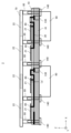
- the antenna device 2 in this embodiment is an array antenna device including a substrate 10, a plurality of antenna elements 21, a power supply circuit 30, a conductor 41, an antenna element power supply section 60, a radome 70, a radome connection section 80, an antenna element 22, and a bandpass filter 90.
- Antenna device 2 is a device that performs transmission processing of radio frequency signals.
- An electrical wiring pattern is provided on the substrate 10 of the antenna device 2, and a plurality of antenna elements 21 are arranged on a first surface, which is one side of the substrate 10.
- the plurality of antenna elements 21 are arranged along the X direction in FIG. 2.
- the substrate 10 may be referred to as a printed circuit board.
- the substrate 10 may be, for example, a general-purpose glass epoxy substrate, but is not limited to this.
- the antenna element 21 of the antenna device 2 is disposed on a first surface, which is one side of the substrate 10.
- the first surface is the direction of radio wave emission from the antenna element 21, and may be referred to as the front surface or upper surface.
- the second surface of the substrate 10, which is opposite to the first surface, may be referred to as the back surface or lower surface.
- the antenna element 21 functions as a primary resonator for transmitting and receiving signals by the transceiver 100, which will be described later.
- the multiple antenna elements 21 are disposed on the first surface of the substrate 10 at a predetermined distance apart.
- the antenna element 21 may be, for example, a patch antenna or a dipole antenna, but is not limited to these.
- the antenna device 2 emits radio waves from the antenna element 22 in the Z direction in FIG. 2 (the direction in which the first surface of the substrate 10 is oriented) due to dual resonance between the antenna element 21 and the antenna element 22 described below, making it possible to transmit and receive signals to and from a communication device in that direction.
- the power supply circuit 30 of the antenna device 2 is disposed on the second surface, which is the reverse side of the first surface of the substrate 10.
- the power supply circuit 30 is a circuit that supplies power to the multiple antenna elements 21.
- the power supply circuit 30 is disposed along the multiple antenna elements 21.
- the power supply circuit 30 distributes power to the multiple antenna elements 21.
- the power supply circuit 30 is electrically connected to an antenna element power supply unit 60, which will be described later.
- the power supply circuit 30 is connected to a connector 130, which will be described later. In FIG. 2, the power supply circuit 30 is connected to the connector 130 on the second surface side of the substrate 10, passes through the first surface side of the substrate 10, and is again formed on the second surface side of the substrate 10.
- the power supply circuit 30 may be connected to the connector 130 on the second surface side of the substrate 10, and may be formed only on the second surface side without passing through the first surface side of the substrate 10.
- the connector 130 may be a coaxial connector, but is not limited thereto.
- the conductor 41 of the antenna device 2 serves as a first conductor and is disposed in a position facing the power supply circuit 30.
- the conductor 41 functions as a ground for the power supply circuit 30.
- a portion of the conductor 41 is adjacent to the substrate 10.
- the material of the conductor 41 may be, for example, a metal, but is not limited to this.
- the conductor 41 may be formed in combination with an insulator as long as at least the surface is a conductor.
- the conductor 41 may be formed by covering the surface of an insulating material such as plastic or resin with a conductor such as metal plating.
- a gap 51 is formed between the power supply circuit 30 and the conductor 41.
- the gap 51 is, for example, an air layer. The positional relationship between the power supply circuit 30, the conductor 41, and the gap 51 will be described in detail with reference to FIG. 3.
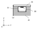
- FIG. 3 is a cross-sectional view of the antenna device 2 of this embodiment. Specifically, FIG. 3 is a cross-sectional view of the antenna device 2 of this embodiment shown in FIG. 2 at the dotted line portion (a).
- the void 51 is formed along the power supply circuit 30. Electromagnetic waves generated from the power supply circuit 30 propagate through the void 51.
- the void 51 may be formed in a rectangular parallelepiped shape as shown in FIG. 3, but is not limited to this.
- the void 51 is further formed so as to be surrounded by the substrate 10 and the conductor 41.
- the void 51 may be formed by cutting a part of the rectangular parallelepiped conductor 41 and placing it adjacent to the substrate 10. Alternatively, the void 51 may be formed by placing the conductor 41 cast in a U-shape adjacent to the substrate 10.
- the shape of the conductor 41 that forms the void 51 and the method of creating that shape are not limited to the above.
- the size of the gap 51 may be determined by the characteristic impedance, but is not limited to this.
- the size of the gap 51 may be determined by the characteristic impedance of the connector 130, for example.
- the characteristic impedance of the connector 130 may be 50 ⁇ .
- Components that affect the characteristic impedance include the width of the power supply circuit 30 and the distance from the second surface of the substrate 10 to the surface of the conductor 41 that faces the second surface of the substrate 10. In other words, components that affect the characteristic impedance include the Y-direction dimension of the power supply circuit 30 in FIG. 3 and the Z-direction dimension of the gap 51 in FIG. 3.
- the distance between the side surfaces of the conductor 41 adjacent to the gap 51 (the Y-direction dimension of the gap 51), indicated by the bidirectional arrow in FIG. 3, as long as possible. This is because the distance between the side surfaces of the conductor 41 adjacent to the gap 51 affects the characteristic impedance if it is shorter than a certain value.
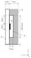
- FIG. 4 is a diagram showing an example of dimensions in the cross section of the antenna device 2 of this embodiment shown in FIG. 3.
- the example dimensions of the antenna device 2 shown in FIG. 4 are an example of design and are not limited thereto.
- the distance from the second surface of the substrate 10 to the surface of the conductor 41 facing the second surface of the substrate 10 may be, for example, 0.5 mm.
- the width of the power supply circuit 30 (the dimension in the Y direction of the power supply circuit 30 in FIG. 4) may be, for example, 2.0 mm.
- the distance between the side surfaces of the conductor 41 adjacent to the gap 51 (the dimension in the Y direction of the gap 51 in FIG. 4) may be, for example, 8.0 mm or more.
- the thickness of the substrate 10 (the dimension in the Z direction of the substrate 10 in FIG. 4) may be 1.0 mm.
- the thickness of the conductor 41 may be 1.5 mm.
- the distance between one end of the power supply circuit 30 and the side of the conductor 41 adjacent to the gap 51 (the dimension in the Y direction between one end of the power supply circuit 30 and one end of the gap 51 in FIG. 4) may be 3.0 mm.
- the antenna element power supply section 60 of the antenna device 2 connects the power supply circuit 30 arranged on the second surface of the substrate 10 to the antenna element 21.
- the antenna element power supply section 60 may be a through hole formed in the substrate 10, but is not limited to this.
- the radome 70 of the antenna device 2 is disposed opposite to the first surface of the substrate 10 and covers the first surface.
- the radome 70 is connected to the substrate 10 via a radome connection part 80 described later.
- the radome 70 has a function of protecting the first surface of the substrate 10 and the antenna element 21.
- the radome 70 has a function of dissipating heat generated in the antenna device 2 or in a radio connected to the antenna device 2 to the outside.
- the main heat source of the heat generated in the antenna device 2 or in a radio connected to the antenna device 2 is, for example, a transceiver 100 described later.
- the transceiver 100 is thermally connected to the conductor 41 via a bandpass filter 90 described later.
- the heat from the transceiver 100 propagates through the conductor 41 and is transferred to the radome 70.
- the heat source and the conductor 41 may be adjacent and directly connected. Also, the heat source and the conductor 41 may be connected via another component, and the heat from the heat source may be transferred to the conductor 41 via the other component.
- the other part may be a metal part, but is not limited to this.
- the material of the radome 70 may be, for example, a resin, or a metal having high thermal conductivity, such as aluminum, silver, or copper.
- the radome 70 may be, for example, made of the same material as the conductor 41.
- the radome 70 may be thermally connected to the conductor 41. However, the material of the radome 70 is not limited to the above.
- the radome connection part 80 of the antenna device 2 connects the substrate 10 and the radome 70.
- the radome 70 and the radome connection part 80 serve as the second conductor.
- the radome connection part 80 is fixed to the conductor 41 and the substrate 10 by the fastening part 140.
- the fastening part 140 may be, for example, a screw, but is not limited to this.
- the antenna element 22 of the antenna device is disposed on the radome 70.
- the multiple antenna elements 22 are arranged along the X direction in FIG. 2.
- the multiple antenna elements 22 are disposed on the radome 70 at a predetermined distance apart.
- the antenna element 22 is disposed in a position facing the antenna element 21.
- the antenna element 22 may be, for example, a slot antenna, but is not limited to this.
- the antenna element 22 couples and resonates with the antenna element 21.
- the bandpass filter 90 of the antenna device 2 is connected to the power supply circuit 30 via the connector 130.
- the bandpass filter 90 is also connected to the conductor 41.
- the antenna device 2 of this embodiment has the structure shown in Figures 2 and 3, and thus has the same effect as the first embodiment. Furthermore, the antenna device 2 of this embodiment can adjust and maintain the size of the gap by using the shape of the conductor 41. Therefore, compared to the antenna device 3 of the third embodiment described below, it is possible to maintain a higher dimensional accuracy of the gap. This makes it possible to maintain a reduction in dielectric loss during power supply.
- the antenna device 2 in this embodiment may be mounted on a wireless device.
- An example of a wireless device 5 having the antenna device 2 in this embodiment is shown in FIG. 5.
- the wireless device 5 shown in FIG. 5 is a device that performs wireless communication, and includes the antenna device 2 in this embodiment and a transceiver 100.
- the transceiver 100 is a mechanism for the antenna device 2 to transmit and receive signals.
- the transceiver 100 may be disposed adjacent to the bandpass filter 90.
- the transceiver 100 may also be referred to as a transceiver, an RF (Radio Frequency) circuit, or an amplifier.
- the radome 70 and antenna element 22 of the antenna device 2 are located on the surface of the wireless device 5. As shown in FIG. 5, the radome 70 of the antenna device 2 may be extended to cover the surface of the wireless device 5.
- the wireless device 5 shown in FIG. 5 is, for example, a base station device.
- the base station device may be, for example, a Node B, an e-Node B, a g-Node B, a Home Node B, or a Home e-Node B.
- a base station device equipped with the antenna device 2 of this embodiment can increase the equivalent isotropic radiated power compared to a base station device equipped with a conventional antenna device.
- the wireless device 5 equipped with the antenna device 2 of this embodiment is not limited to a base station device, and may be other wireless devices that perform wireless communication.
- the heat transfer path from the heat source to the radome includes the substrate, which reduces the heat transfer efficiency.
- the heat transfer path from the heat source to the radome 70 is the heat source, conductor 41, fastening part 140, radome connection part 80, and radome 70. Therefore, by forming the conductor 41, fastening part 140, and radome connection part 80 from a material with high thermal conductivity, the heat dissipation effect can be improved.
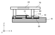
- the conductor 41 of the antenna device 2 and the radome connecting portion 80 are thermally connected by using the fastening portion 140.
- a hole may be formed in the substrate 10 and the conductor 41 and the radome connecting portion 80 may be directly connected to each other.
- a conductor connection portion 110 is disposed on a part of the substrate 10.
- the conductor connection portion 110 is disposed on a portion of the substrate 10 that contacts the conductor 41 and the radome connection portion 80.
- the conductor connection portion 110 may also be a protrusion formed on the radome connection portion 80 or the conductor 41.
- it may be a protrusion provided on the surface of the radome connection portion 80 adjacent to the substrate 10. The protrusion may protrude from the radome connection portion 80 in the opposite direction to the Z-direction arrow in FIG. 6.
- the conductor connection portion 110 may be a protrusion provided on the surface of the conductor 41 adjacent to the substrate 10.
- the protrusion may protrude from the conductor connection portion 110 in the same direction as the Z-direction arrow in FIG. 6.
- the conductor 41 and the radome connection portion 80 may be directly connected by drilling a hole in the portion of the substrate 10 that contacts the conductor 41 and the radome connection portion 80 and fitting a protrusion into the hole.
- a hole may be formed in the substrate 10, the conductor 41 or the radome connection part 80 may be inserted into the hole, and the conductor 41 and the radome connection part 80 may be directly connected.
- the radome 70, the radome connection part 80, and the conductor connection part 110 are preferably made of a material with high thermal conductivity.
- the radome 70, the radome connection part 80, and the conductor connection part 110 may be made of a conductor such as a metal.
- the conductor 41 of the antenna device 2 and the radome connecting portion 80 are thermally connected by using the fastening portion 140.
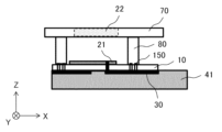
- the conductor 41 and the radome connecting portion 80 may be thermally connected by providing a through hole 150 in a part of the substrate 10.
- FIG. 7 is an enlarged view showing the configuration of the antenna device 2 in the second modified example of this embodiment.
- a plurality of through holes 150 are formed in the substrate 10.
- the through holes 150 are formed in a portion of the substrate 10 that contacts the conductor 41 and the radome connection portion 80. That is, the conductor 41 and the radome connection portion 80 are connected via the through holes 150 formed in the substrate 10.
- the conductor 41 and the radome connection portion 80 are connected in the Z direction in FIG. 7 via the through holes 150.
- the radome 70 and the radome connection portion 80 are preferably formed of a material with high thermal conductivity.
- the radome 70 and the radome connection portion 80 may be formed of a conductor such as a metal.
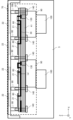
- FIG. 8 is a diagram showing the configuration of the antenna device 3 in this embodiment.
- the antenna device 3 in this embodiment includes a substrate 10, an antenna element 21, a power supply circuit 30, a conductor 42, a support member 120, an antenna element power supply section 60, a radome 70, a radome connection section 80, an antenna element 22, and a bandpass filter 90.
- the conductor 42 of the antenna device 3 is disposed in a position facing the power supply circuit 30 on the second surface of the substrate 10.
- the conductor 42 functions as a ground for the power supply circuit 30.
- the material of the conductor 42 may be, for example, a metal, but is not limited to this.
- the conductor 42 is adjacent to the support member 120 described below.
- the support member 120 of the antenna device 3 is disposed between the conductor 42 and the substrate 10.
- the support member 120 has a function of maintaining the gap 52 between the conductor 42 and the substrate 10 at a predetermined dimension.
- the material of the support member 120 may be, for example, a metal, but is not limited to this.
- the support member 120 may also be referred to as a spacer.
- the shape of the support member 120 may be, for example, a rectangular parallelepiped, but is not limited to this.
- a gap 52 is formed between the power supply circuit 30, the conductor 42, and the support member 120.
- the gap 52 is, for example, an air layer. The positional relationship between the power supply circuit 30, the conductor 42, the support member 120, and the gap 52 will be described in detail with reference to FIG. 9.
- FIG. 9 is a cross-sectional view of the antenna device 3 of this embodiment.
- FIG. 9 is a cross-sectional view of the antenna device 3 of this embodiment shown in FIG. 8 at the dotted line portion (b).
- the void 52 is formed along the power supply circuit 30. Electromagnetic waves generated from the power supply circuit 30 propagate through the void 52.
- the void 52 may be formed in a rectangular parallelepiped shape as shown in FIG. 9, but is not limited to this.
- the void 52 is further formed so as to be surrounded by the substrate 10, the conductor 42, and the support member 120.
- the size of the gap 52 may be determined by the characteristic impedance, but is not limited to this.
- the size of the gap 52 may be determined by, for example, the characteristic impedance of the connector 130.
- the characteristic impedance of the connector 130 may be 50 ⁇ .
- Components that affect the characteristic impedance include the width of the power supply circuit 30 and the distance from the second surface of the substrate 10 to the surface of the conductor 42 facing the second surface of the substrate 10. In other words, components that affect the characteristic impedance include the Y-direction dimension of the power supply circuit 30 in FIG. 9 and the Z-direction dimension of the gap 52 in FIG. 3.
- the distance from the second surface of the substrate 10 to the surface of the conductor 42 facing the second surface of the substrate 10 may be, for example, 0.5 mm.
- the distance between the sides of the support member 120 adjacent to the gap 52 may be, for example, 8.0 mm or more.
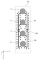
- FIG. 10 is an example of the arrangement of the support members 120 in this embodiment.
- the support members 120 may be arranged in a plurality of locations along the outer periphery of the substrate 10.
- the support members 120 may be arranged at regular intervals. When the support members 120 are arranged sparsely as in FIG. 10, the number of support members 120 used is small, and therefore costs can be reduced.
- the support members 120 may be arranged densely along the outer periphery of the substrate 10.
- FIG. 11 is also an example of the arrangement of the support members 120 in this embodiment. As shown in FIG. 11, the support members 120 may be arranged in a plurality of locations along the power supply circuit 30. When the support members 120 are arranged densely as in FIG.
- the dimensions of the gaps 52 are likely to be kept constant.
- the heat dissipation efficiency is higher than when the support members 120 are arranged sparsely.
- the support members 120 may be arranged sparsely along the power supply circuit 30.
- the antenna device 3 of this embodiment has the same effects as the second embodiment by having the structure shown in Figures 8 to 11. Moreover, the antenna device 3 of this embodiment is easier to design so that the mass of the conductor is smaller than that of the antenna device 2 of the second embodiment, so that it is possible to achieve low cost and low mass. Moreover, the antenna device 3 in this embodiment may be mounted on a wireless device, similar to the antenna device 2 in the second embodiment.
- An example of a wireless device 6 having the antenna device 3 in this embodiment is shown in Fig. 12.
- the wireless device 6 shown in Fig. 12 is a device that performs wireless communication, and has the antenna device 3 in this embodiment and a transceiver 100.
- the transceiver 100 may be the same as the transceiver included in the wireless device 6 shown in Fig. 5.
- the radome 70 and antenna element 22 of the antenna device 3 are located on the surface of the wireless device 6. Note that, as shown in Fig. 12, the radome 70 of the antenna device 3 may be extended to cover the surface of the wireless device 6.
- the wireless device 6 shown in FIG. 12 is, for example, a base station device.
- the base station device may be, for example, a Node B, an e-Node B, a g-Node B, a Home Node B, or a Home e-Node B.
- a base station device equipped with the antenna device 3 of this embodiment can increase the equivalent isotropic radiated power compared to a base station device equipped with a conventional antenna device. In addition, it can achieve lower costs and lower mass compared to a base station device equipped with the antenna device 2 of the second embodiment.
- the wireless device 6 equipped with the antenna device 3 of this embodiment is not limited to a base station device, and may be other wireless devices that perform wireless communication.
- (Appendix 1) A substrate; a plurality of antenna elements disposed on a first surface of the substrate; a power supply circuit disposed on a second surface of the substrate, the second surface being a surface opposite to the first surface; a first conductor disposed at a position facing the power supply circuit; an air gap is formed between the power supply circuit and the first conductor; Antenna device. (Appendix 2) The gap is formed along the power supply circuit. 2. The antenna device of claim 1. (Appendix 3) a portion of the first conductor adjacent to the substrate; The gap is formed so as to be surrounded by the substrate and the first conductor. 3. The antenna device according to claim 2.
- (Appendix 4) a support member disposed between the first conductor and the substrate; the gap is formed by the substrate, the first conductor, and the support member.
- the antenna device of claim 1. (Appendix 5) The member is arranged in plurality along the outer periphery of the substrate. 5.
- the antenna device according to claim 4. (Appendix 6) The member is arranged in plurality along the power supply circuit. 5.
- the antenna device according to claim 4. (Appendix 7) an antenna element feeding section that connects the plurality of antenna elements and the feeding circuit; 7.
- the antenna device of claim 8. (Appendix 10) the first conductor and the connection portion are connected via a through hole formed in the substrate, the radome and the connection portion are a second conductor; 9.
- the antenna device of claim 8. (Appendix 11)
- the antenna element feed portion is a through hole formed in the substrate. 8.
- the plurality of antenna elements include patch antennas; 5.
- the plurality of antenna elements include a dipole antenna; 5.
- the antenna device according to claim 3 or 4. The antenna device is an array antenna device. 5.
- the antenna device according to claim 3 or 4. (Appendix 15)
- the substrate includes a glass epoxy substrate. 5.
- the antenna device according to claim 3 or 4. (Appendix 16) the first conductor is a metal; 5.
- the antenna device according to claim 3 or 4. (Appendix 17) the second conductor is a metal; 11.
- a substrate A substrate; a plurality of antenna elements disposed on a first surface of the substrate; a power supply circuit disposed on a second surface of the substrate, the second surface being a surface opposite to the first surface, and configured to distribute power to the plurality of antenna elements; a conductor that is disposed in a position facing the power supply circuit and functions as a ground of the power supply circuit; An air gap is formed between the power supply circuit and the conductor.
- Antenna device A substrate; a plurality of antenna elements disposed on a first surface of the substrate; a power supply circuit disposed on a second surface of the substrate, the second surface being a surface opposite to the first surface, and configured to distribute power to the plurality of antenna elements; a conductor that is disposed in a position facing the power supply circuit and functions as a ground of the power supply circuit; An air gap is formed between the power supply circuit and the conductor.
- a substrate A substrate; a plurality of antenna elements disposed on a first surface of the substrate; a power supply circuit disposed on a second surface of the substrate, the second surface being a surface opposite to the first surface; a first conductor disposed at a position facing the power supply circuit; an air gap is formed between the power supply circuit and the first conductor; An antenna device; A transceiver; Wireless device.
Landscapes
- Details Of Aerials (AREA)
Abstract
Description
図1は、本開示の第1実施形態におけるアンテナ装置1の構成を示す図である。
本開示の第2実施形態におけるアンテナ装置2について説明する。
本実施形態では、アンテナ装置2の導体41とレドーム接続部80とを、締結部140を用いて熱的に接続している。これに代えて、基板10に穴を空け、導体41とレドーム接続部80とを直接接続してもよい。
本実施形態では、アンテナ装置2の導体41とレドーム接続部80とを、締結部140を用いて熱的に接続している。これに代えて、基板10の一部にスルーホール150を設けることで、導体41とレドーム接続部80とを熱的に接続してもよい。
本開示の第3実施形態におけるアンテナ装置3について説明する。なお、以下において第2実施形態と同様の構成については同一の符号を付し、その説明を省略する。
また、本実施形態におけるアンテナ装置3は、第2実施形態のアンテナ装置2と同様、無線装置に搭載されることとしてもよい。本実施形態におけるアンテナ装置3を有する無線装置6の例を図12に示す。図12に示す無線装置6は、無線通信を行う装置であって、本実施形態におけるアンテナ装置3と、送受信機100とを有する。送受信機100は、図5に示す無線装置6が有する送受信機と同様であってもよい。アンテナ装置3のレドーム70とアンテナ素子22とは、無線装置6の表面に位置する。なお、図12のように、アンテナ装置3のレドーム70は無線装置6の表面を覆うように延長されてもよい。
(付記1)
基板と、
前記基板の第1面に配置された複数のアンテナ素子と、
前記基板の前記第1面の裏面である第2面に配置された給電回路と、
前記給電回路に対向する位置に配置された第1の導体と、を備え、
前記給電回路と前記第1の導体との間には空隙が形成されている、
アンテナ装置。
(付記2)
前記空隙は、前記給電回路に沿って形成されている、
付記1に記載のアンテナ装置。
(付記3)
前記第1の導体の一部は前記基板に隣接し、
前記空隙は、前記基板と、前記第1の導体とで囲うように形成されている、
付記2に記載のアンテナ装置。
(付記4)
前記第1の導体と前記基板との間に配置された支持部材をさらに備え、
前記空隙は、前記基板と、前記第1の導体と、前記支持部材と、で形成されている、
付記1に記載のアンテナ装置。
(付記5)
前記部材は、前記基板の外周に沿って複数配置されている、
付記4に記載のアンテナ装置。
(付記6)
前記部材は、前記給電回路に沿って複数配置されている、
付記4に記載のアンテナ装置。
(付記7)
前記複数のアンテナ素子と前記給電回路を接続するアンテナ素子給電部を備える、
付記1乃至6のいずれか一項に記載のアンテナ装置。
(付記8)
前記基板の前記第1面側を覆うレドームと、
前記基板と前記レドームとを接続する接続部と、をさらに備える、
付記7に記載のアンテナ装置。
(付記9)
前記基板には穴が形成され、
前記第1の導体もしくは前記接続部が前記穴に挿入され、前記第1の導体と前記接続部が直接接続されており、
前記レドームおよび前記接続部は第2の導体である、
付記8に記載のアンテナ装置。
(付記10)
前記第1の導体と前記接続部が、前記基板に形成されたスルーホールを介して接続されており、
前記レドームおよび前記接続部は第2の導体である、
付記8に記載のアンテナ装置。
(付記11)
前記アンテナ素子給電部は、前記基板に形成されたスルーホールである、
付記7に記載のアンテナ装置。
(付記12)
前記複数のアンテナ素子はパッチアンテナを含む、
付記3又は4に記載のアンテナ装置。
(付記13)
前記複数のアンテナ素子はダイポールアンテナを含む、
付記3又は4に記載のアンテナ装置。
(付記14)
前記アンテナ装置は、アレーアンテナ装置である、
付記3又は4に記載のアンテナ装置。
(付記15)
前記基板は、ガラスエポキシ基板を含む、
付記3又は4に記載のアンテナ装置。
(付記16)
前記第1の導体は、金属である、
付記3又は4に記載のアンテナ装置。
(付記17)
前記第2の導体は、金属である、
付記9又は10に記載のアンテナ装置。
(付記18)
基板と、
前記基板の第1面に配置された複数のアンテナ素子と、
前記基板の前記第1面の裏面である第2面に配置され、前記複数のアンテナ素子に電力を分配する給電回路と、
前記給電回路に対向する位置に配置され、前記給電回路のグランドとして機能する導体と、を備え、
前記給電回路と前記導体との間には空隙が形成されている、
アンテナ装置。
(付記19)
基板と、
前記基板の第1面に配置された複数のアンテナ素子と、
前記基板の前記第1面の裏面である第2面に配置された給電回路と、
前記給電回路に対向する位置に配置された第1の導体と、を備え、
前記給電回路と前記第1の導体との間には空隙が形成されている、
アンテナ装置と、
送受信機と、を備える、
無線装置。
5、6 無線装置
10 基板
20、21、22 アンテナ素子
30 給電回路
40、41、42 導体
50、51、52 空隙
60 アンテナ素子給電部
70 レドーム
80 レドーム接続部
90 バンドパスフィルタ
100 送受信機
110 導体接続部
120 支持部材
130 コネクタ
140 締結部
150 スルーホール
Claims (19)
- 基板と、
前記基板の第1面に配置された複数のアンテナ素子と、
前記基板の前記第1面の裏面である第2面に配置された給電回路と、
前記給電回路に対向する位置に配置された第1の導体と、を備え、
前記給電回路と前記第1の導体との間には空隙が形成されている、
アンテナ装置。 - 前記空隙は、前記給電回路に沿って形成されている、
請求項1に記載のアンテナ装置。 - 前記第1の導体の一部は前記基板に隣接し、
前記空隙は、前記基板と、前記第1の導体とで囲うように形成されている、
請求項2に記載のアンテナ装置。 - 前記第1の導体と前記基板との間に配置された支持部材をさらに備え、
前記空隙は、前記基板と、前記第1の導体と、前記支持部材と、で形成されている、
請求項1に記載のアンテナ装置。 - 前記支持部材は、前記基板の外周に沿って複数配置されている、
請求項4に記載のアンテナ装置。 - 前記支持部材は、前記給電回路に沿って複数配置されている、
請求項4に記載のアンテナ装置。 - 前記複数のアンテナ素子と前記給電回路を接続するアンテナ素子給電部を備える、
請求項1乃至6のいずれか一項に記載のアンテナ装置。 - 前記基板の前記第1面側を覆うレドームと、
前記基板と前記レドームとを接続する接続部と、をさらに備える、
請求項7に記載のアンテナ装置。 - 前記基板には穴が形成され、
前記第1の導体もしくは前記接続部が前記穴に挿入され、前記第1の導体と前記接続部が直接接続されており、
前記レドームおよび前記接続部は第2の導体である、
請求項8に記載のアンテナ装置。 - 前記第1の導体と前記接続部が、前記基板に形成されたスルーホールを介して接続されており、
前記レドームおよび前記接続部は第2の導体である、
請求項8に記載のアンテナ装置。 - 前記アンテナ素子給電部は、前記基板に形成されたスルーホールである、
請求項7に記載のアンテナ装置。 - 前記複数のアンテナ素子はパッチアンテナを含む、
請求項3又は4に記載のアンテナ装置。 - 前記複数のアンテナ素子はダイポールアンテナを含む、
請求項3又は4に記載のアンテナ装置。 - 前記アンテナ装置は、アレーアンテナ装置である、
請求項3又は4に記載のアンテナ装置。 - 前記基板は、ガラスエポキシ基板を含む、
請求項3又は4に記載のアンテナ装置。 - 前記第1の導体は、金属である、
請求項3又は4に記載のアンテナ装置。 - 前記第2の導体は、金属である、
請求項9又は10に記載のアンテナ装置。 - 基板と、
前記基板の第1面に配置された複数のアンテナ素子と、
前記基板の前記第1面の裏面である第2面に配置され、前記複数のアンテナ素子に電力を分配する給電回路と、
前記給電回路に対向する位置に配置され、前記給電回路のグランドとして機能する導体と、を備え、
前記給電回路と前記導体との間には空隙が形成されている、
アンテナ装置。 - 基板と、
前記基板の第1面に配置された複数のアンテナ素子と、
前記基板の前記第1面の裏面である第2面に配置された給電回路と、
前記給電回路に対向する位置に配置された第1の導体と、を備え、
前記給電回路と前記第1の導体との間には空隙が形成されている、
アンテナ装置と、
送受信機と、を備える、
無線装置。
Priority Applications (2)
| Application Number | Priority Date | Filing Date | Title |
|---|---|---|---|
| JP2025505039A JPWO2024185136A5 (ja) | 2023-03-09 | アンテナ装置 | |
| PCT/JP2023/009102 WO2024185136A1 (ja) | 2023-03-09 | 2023-03-09 | アンテナ装置及び無線装置 |
Applications Claiming Priority (1)
| Application Number | Priority Date | Filing Date | Title |
|---|---|---|---|
| PCT/JP2023/009102 WO2024185136A1 (ja) | 2023-03-09 | 2023-03-09 | アンテナ装置及び無線装置 |
Publications (1)
| Publication Number | Publication Date |
|---|---|
| WO2024185136A1 true WO2024185136A1 (ja) | 2024-09-12 |
Family
ID=92674567
Family Applications (1)
| Application Number | Title | Priority Date | Filing Date |
|---|---|---|---|
| PCT/JP2023/009102 Ceased WO2024185136A1 (ja) | 2023-03-09 | 2023-03-09 | アンテナ装置及び無線装置 |
Country Status (1)
| Country | Link |
|---|---|
| WO (1) | WO2024185136A1 (ja) |
Citations (3)
| Publication number | Priority date | Publication date | Assignee | Title |
|---|---|---|---|---|
| JPH06260830A (ja) * | 1993-02-04 | 1994-09-16 | Electronique Serge Dassault | 特にuhf受信器のための、改善されたマイクロストリップアンテナ装置 |
| JP2013219723A (ja) * | 2012-04-12 | 2013-10-24 | Hitachi Cable Ltd | アンテナ装置 |
| WO2022176285A1 (ja) * | 2021-02-17 | 2022-08-25 | 日本電気株式会社 | アンテナ装置及びレドーム |
-
2023
- 2023-03-09 WO PCT/JP2023/009102 patent/WO2024185136A1/ja not_active Ceased
Patent Citations (3)
| Publication number | Priority date | Publication date | Assignee | Title |
|---|---|---|---|---|
| JPH06260830A (ja) * | 1993-02-04 | 1994-09-16 | Electronique Serge Dassault | 特にuhf受信器のための、改善されたマイクロストリップアンテナ装置 |
| JP2013219723A (ja) * | 2012-04-12 | 2013-10-24 | Hitachi Cable Ltd | アンテナ装置 |
| WO2022176285A1 (ja) * | 2021-02-17 | 2022-08-25 | 日本電気株式会社 | アンテナ装置及びレドーム |
Also Published As
| Publication number | Publication date |
|---|---|
| JPWO2024185136A1 (ja) | 2024-09-12 |
Similar Documents
| Publication | Publication Date | Title |
|---|---|---|
| TWI425713B (zh) | 諧振產生之三頻段天線 | |
| US7755545B2 (en) | Antenna and method of manufacturing the same, and portable wireless terminal using the same | |
| US9698487B2 (en) | Array antenna | |
| US6876328B2 (en) | Multiple-resonant antenna, antenna module, and radio device using the multiple-resonant antenna | |
| CN102255126B (zh) | 无线通信装置 | |
| CN109478721B (zh) | 天线、具有一个或更多个天线的装置及通信装置 | |
| US11973278B2 (en) | Antenna structure and electronic device | |
| JP3139975B2 (ja) | アンテナ装置 | |
| CN104185926B (zh) | 天线装置 | |
| CN103378412A (zh) | 天线装置 | |
| JP5213039B2 (ja) | 片面放射アンテナ | |
| US6697023B1 (en) | Built-in multi-band mobile phone antenna with meandering conductive portions | |
| JP2008219627A (ja) | マイクロストリップアンテナ | |
| JP3002277B2 (ja) | 平面アンテナ | |
| CN116995415A (zh) | 一种天线 | |
| CN118645791A (zh) | 天线装置 | |
| JP3514305B2 (ja) | チップアンテナ | |
| CN114583448A (zh) | 一种用于5g移动通信的紧凑型三单元终端mimo天线阵 | |
| JP3824998B2 (ja) | 誘電体導波管アンテナ | |
| CN220774736U (zh) | 天线结构及终端设备 | |
| WO2024185136A1 (ja) | アンテナ装置及び無線装置 | |
| CN118712716B (zh) | 一种电子设备 | |
| US7598912B2 (en) | Planar antenna structure | |
| CN115513655B (zh) | 集成天线及电子设备 | |
| CN218498380U (zh) | 缝隙天线和电子设备 |
Legal Events
| Date | Code | Title | Description |
|---|---|---|---|
| 121 | Ep: the epo has been informed by wipo that ep was designated in this application |
Ref document number: 23926346 Country of ref document: EP Kind code of ref document: A1 |
|
| ENP | Entry into the national phase |
Ref document number: 2025505039 Country of ref document: JP Kind code of ref document: A |
|
| WWE | Wipo information: entry into national phase |
Ref document number: 2025505039 Country of ref document: JP |
|
| NENP | Non-entry into the national phase |
Ref country code: DE |
|
| 122 | Ep: pct application non-entry in european phase |
Ref document number: 23926346 Country of ref document: EP Kind code of ref document: A1 |