WO2024181533A1 - 光学積層体、並びに、前記光学積層体を用いた偏光板、表面板、画像表示パネル及び画像表示装置 - Google Patents
光学積層体、並びに、前記光学積層体を用いた偏光板、表面板、画像表示パネル及び画像表示装置 Download PDFInfo
- Publication number
- WO2024181533A1 WO2024181533A1 PCT/JP2024/007546 JP2024007546W WO2024181533A1 WO 2024181533 A1 WO2024181533 A1 WO 2024181533A1 JP 2024007546 W JP2024007546 W JP 2024007546W WO 2024181533 A1 WO2024181533 A1 WO 2024181533A1
- Authority
- WO
- WIPO (PCT)
- Prior art keywords
- refractive index
- optical laminate
- less
- low refractive
- index layer
- Prior art date
- Legal status (The legal status is an assumption and is not a legal conclusion. Google has not performed a legal analysis and makes no representation as to the accuracy of the status listed.)
- Ceased
Links
Images


Classifications
-
- G—PHYSICS
- G02—OPTICS
- G02B—OPTICAL ELEMENTS, SYSTEMS OR APPARATUS
- G02B1/00—Optical elements characterised by the material of which they are made; Optical coatings for optical elements
- G02B1/10—Optical coatings produced by application to, or surface treatment of, optical elements
- G02B1/11—Anti-reflection coatings
- G02B1/111—Anti-reflection coatings using layers comprising organic materials
-
- B—PERFORMING OPERATIONS; TRANSPORTING
- B32—LAYERED PRODUCTS
- B32B—LAYERED PRODUCTS, i.e. PRODUCTS BUILT-UP OF STRATA OF FLAT OR NON-FLAT, e.g. CELLULAR OR HONEYCOMB, FORM
- B32B27/00—Layered products comprising a layer of synthetic resin
- B32B27/18—Layered products comprising a layer of synthetic resin characterised by the use of special additives
- B32B27/20—Layered products comprising a layer of synthetic resin characterised by the use of special additives using fillers, pigments, thixotroping agents
-
- B—PERFORMING OPERATIONS; TRANSPORTING
- B32—LAYERED PRODUCTS
- B32B—LAYERED PRODUCTS, i.e. PRODUCTS BUILT-UP OF STRATA OF FLAT OR NON-FLAT, e.g. CELLULAR OR HONEYCOMB, FORM
- B32B3/00—Layered products comprising a layer with external or internal discontinuities or unevennesses, or a layer of non-planar shape; Layered products comprising a layer having particular features of form
- B32B3/26—Layered products comprising a layer with external or internal discontinuities or unevennesses, or a layer of non-planar shape; Layered products comprising a layer having particular features of form characterised by a particular shape of the outline of the cross-section of a continuous layer; characterised by a layer with cavities or internal voids ; characterised by an apertured layer
- B32B3/30—Layered products comprising a layer with external or internal discontinuities or unevennesses, or a layer of non-planar shape; Layered products comprising a layer having particular features of form characterised by a particular shape of the outline of the cross-section of a continuous layer; characterised by a layer with cavities or internal voids ; characterised by an apertured layer characterised by a layer formed with recesses or projections, e.g. hollows, grooves, protuberances, ribs
-
- B—PERFORMING OPERATIONS; TRANSPORTING
- B32—LAYERED PRODUCTS
- B32B—LAYERED PRODUCTS, i.e. PRODUCTS BUILT-UP OF STRATA OF FLAT OR NON-FLAT, e.g. CELLULAR OR HONEYCOMB, FORM
- B32B7/00—Layered products characterised by the relation between layers; Layered products characterised by the relative orientation of features between layers, or by the relative values of a measurable parameter between layers, i.e. products comprising layers having different physical, chemical or physicochemical properties; Layered products characterised by the interconnection of layers
- B32B7/02—Physical, chemical or physicochemical properties
- B32B7/023—Optical properties
-
- G—PHYSICS
- G02—OPTICS
- G02B—OPTICAL ELEMENTS, SYSTEMS OR APPARATUS
- G02B1/00—Optical elements characterised by the material of which they are made; Optical coatings for optical elements
- G02B1/04—Optical elements characterised by the material of which they are made; Optical coatings for optical elements made of organic materials, e.g. plastics
-
- G—PHYSICS
- G02—OPTICS
- G02B—OPTICAL ELEMENTS, SYSTEMS OR APPARATUS
- G02B5/00—Optical elements other than lenses
- G02B5/02—Diffusing elements; Afocal elements
-
- G—PHYSICS
- G02—OPTICS
- G02B—OPTICAL ELEMENTS, SYSTEMS OR APPARATUS
- G02B5/00—Optical elements other than lenses
- G02B5/20—Filters
-
- G—PHYSICS
- G02—OPTICS
- G02B—OPTICAL ELEMENTS, SYSTEMS OR APPARATUS
- G02B5/00—Optical elements other than lenses
- G02B5/30—Polarising elements
-
- G—PHYSICS
- G02—OPTICS
- G02F—OPTICAL DEVICES OR ARRANGEMENTS FOR THE CONTROL OF LIGHT BY MODIFICATION OF THE OPTICAL PROPERTIES OF THE MEDIA OF THE ELEMENTS INVOLVED THEREIN; NON-LINEAR OPTICS; FREQUENCY-CHANGING OF LIGHT; OPTICAL LOGIC ELEMENTS; OPTICAL ANALOGUE/DIGITAL CONVERTERS
- G02F1/00—Devices or arrangements for the control of the intensity, colour, phase, polarisation or direction of light arriving from an independent light source, e.g. switching, gating or modulating; Non-linear optics
- G02F1/01—Devices or arrangements for the control of the intensity, colour, phase, polarisation or direction of light arriving from an independent light source, e.g. switching, gating or modulating; Non-linear optics for the control of the intensity, phase, polarisation or colour
- G02F1/13—Devices or arrangements for the control of the intensity, colour, phase, polarisation or direction of light arriving from an independent light source, e.g. switching, gating or modulating; Non-linear optics for the control of the intensity, phase, polarisation or colour based on liquid crystals, e.g. single liquid crystal display cells
- G02F1/133—Constructional arrangements; Operation of liquid crystal cells; Circuit arrangements
- G02F1/1333—Constructional arrangements; Manufacturing methods
- G02F1/1335—Structural association of cells with optical devices, e.g. polarisers or reflectors
- G02F1/133502—Antiglare, refractive index matching layers
-
- G—PHYSICS
- G02—OPTICS
- G02B—OPTICAL ELEMENTS, SYSTEMS OR APPARATUS
- G02B5/00—Optical elements other than lenses
- G02B5/30—Polarising elements
- G02B5/3025—Polarisers, i.e. arrangements capable of producing a definite output polarisation state from an unpolarised input state
Definitions
- This disclosure relates to an optical laminate, as well as a polarizing plate, a face plate, an image display panel, and an image display device that use the optical laminate.
- Optical laminates may be installed on the surfaces of image display devices such as televisions, notebook PCs, and desktop PC monitors to suppress reflections of lighting and people in the background, and to suppress surface reflections.
- an antiglare film having an uneven surface As an optical laminate for suppressing the reflection of the background, an antiglare film having an uneven surface has been proposed. However, the antiglare film has a problem that the contrast is easily reduced due to the scattering of reflected light.
- an antireflection film having an antireflection layer on the surface As an optical laminate for suppressing surface reflection, an antireflection film having an antireflection layer on the surface has been proposed. However, since the antireflection film has a smooth surface shape, it has a problem that it is difficult to suppress the reflection of the background.
- an antiglare antireflection film As an optical laminate for suppressing background reflection and surface reflection, an antiglare antireflection film has been proposed in which an antireflection layer such as a low refractive index layer is laminated on an antiglare layer (Patent Documents 1 and 2, etc.).
- the optical laminates of Patent Documents 1 and 2 have an anti-reflection layer on an anti-glare layer, and therefore can suppress background reflection and surface reflection.
- conventional optical laminates in which an anti-reflection layer is laminated on an anti-glare layer such as the optical laminates of Patent Documents 1 and 2 frequently fail to provide the level of anti-reflection expected at the time of coating design.
- the greater the level of unevenness in the anti-glare layer the more difficult it tends to be to obtain the level of anti-reflection expected at the time of coating design.
- the level of anti-reflection expected at the time of coating design refers to the reflectance calculated by simulation from physical information of the coating design, such as the theoretical refractive index and theoretical film thickness.
- the objective of this disclosure is to provide an optical laminate in which a low refractive index layer is laminated on an antiglare layer, and which provides sufficient anti-reflection properties.
- the present disclosure provides the following ⁇ 1> to ⁇ 5>.
- ⁇ 1> An optical laminate having a first surface and a second surface opposite to the first surface, The optical laminate has a low refractive index layer and an antiglare layer in this order from the first surface to the second surface, the low refractive index layer contains a binder resin and spherical particles having an average particle diameter of 20 nm or more, The first surface has an uneven shape, The "average exclusive area ratio of spherical particles with an average particle size of 20 nm or more" calculated by the following measurement 1 is 15.0% or more, An optical laminate in which the "average film thickness of the low refractive index layer" is 200 nm or less and the “average standard deviation of the film thickness of the low refractive index layer” is 25.0 nm or less, as calculated by the following measurement 2.
- ⁇ Measurement 1> The surface of the first side of the optical laminate is imaged by a scanning electron microscope. The imaging area is adjusted so that the area not including the scale bar is 50.79 ⁇ m wide by 38.10 ⁇ m long. Furthermore, the area of 50.79 ⁇ m wide by 38.10 ⁇ m long is adjusted to have a pixel count of 1280 pixels by 890 pixels. (1-2) The image of the 50.79 ⁇ m horizontal ⁇ 38.10 ⁇ m vertical area of (1-1) above is divided into 256 gradations, with the darkest part being 0 and the brightest part being 255.
- the area ratio of spherical particles with an average particle diameter of 20 nm or more in the 1270 nm wide x 890 nm long region is calculated.
- the above steps (1-1) to (1-4) are carried out at 20 points on the surface of the first surface side of the optical laminate.
- the average of the area ratios of 18 points excluding the minimum and maximum values is defined as the "average exclusive area ratio of spherical particles having an average particle size of 20 nm or more.”
- ⁇ Measurement 2> (2-1)
- the vertical cross section of the optical laminate is imaged using a scanning transmission electron microscope. The image is adjusted so that the area not including the scale bar is 254 ⁇ m wide by 178 ⁇ m long.
- the film thickness of the low refractive index layer is the average value of the film thicknesses at 25 locations.
- the standard deviation of the film thickness of the low refractive index layer is the standard deviation of the film thicknesses at 25 locations.
- the aforementioned 25 locations are selected at 50 nm intervals within a range of 1270 nm long.
- the above steps (2-1) to (2-3) are carried out at 20 points on the vertical cross section of the optical laminate.
- the average thickness and the average standard deviation of the thicknesses at 18 points excluding the minimum and maximum values are defined as the "average thickness of the low refractive index layer" and the "average standard deviation of the thickness of the low refractive index layer.”
- a polarizing plate having a polarizer, a first transparent protective plate arranged on one side of the polarizer, and a second transparent protective plate arranged on the other side of the polarizer, A polarizing plate, wherein at least one of the first transparent protective plate and the second transparent protective plate is the optical laminate described in ⁇ 1>, and the second surface of the optical laminate is arranged opposite the polarizer.
- a face plate for an image display device comprising a protective film bonded to a resin plate or a glass plate, the protective film being the optical laminate according to ⁇ 1>, and the second surface of the optical laminate being disposed opposite the resin plate or the glass plate.
- An image display panel having a display element and an optical laminate arranged on a light exit surface side of the display element, the optical laminate including the optical laminate according to ⁇ 1>.
- An image display device comprising the image display panel according to ⁇ 4>.
- optical laminate, polarizing plate, front plate, image display panel, and image display device disclosed herein can provide good anti-reflection properties.
- FIG. 1 is a schematic cross-sectional view showing one embodiment of an optical laminate of the present disclosure.
- 1 is a cross-sectional view illustrating an embodiment of an image display panel of the present disclosure.
- FIG. 13 is a diagram for explaining measurement 1.
- average occupied area ratio of spherical particles having an average particle size of 20 nm or more may be abbreviated as “average occupied area ratio”.
- the optical laminate of the present disclosure is as follows.
- the optical laminate has a low refractive index layer and an antiglare layer in this order from the first surface to the second surface, the low refractive index layer contains a binder resin and spherical particles having an average particle diameter of 20 nm or more,
- the first surface has an uneven shape,
- the "average exclusive area ratio of spherical particles with an average particle size of 20 nm or more" calculated by the following measurement 1 is 15.0% or more,
- An optical laminate in which the "average film thickness of the low refractive index layer" is 200 nm or less and the “average standard deviation of the film thickness of the low refractive index layer” is 25.0 nm or less, as calculated by the following measurement 2.
- ⁇ Measurement 1> The surface of the first side of the optical laminate is imaged by a scanning electron microscope. The imaging area is adjusted so that the area not including the scale bar is 50.79 ⁇ m wide by 38.10 ⁇ m long. Furthermore, the area of 50.79 ⁇ m wide by 38.10 ⁇ m long is adjusted to have a pixel count of 1280 pixels by 890 pixels. (1-2) The image of the 50.79 ⁇ m horizontal ⁇ 38.10 ⁇ m vertical area of (1-1) above is divided into 256 gradations, with the darkest part being 0 and the brightest part being 255.
- the area ratio of spherical particles with an average particle diameter of 20 nm or more in the 1270 nm wide x 890 nm long region is calculated.
- the above steps (1-1) to (1-4) are carried out at 20 points on the surface of the first surface side of the optical laminate.
- the average of the area ratios of 18 points excluding the minimum and maximum values is defined as the "average exclusive area ratio of spherical particles having an average particle size of 20 nm or more.”
- the low refractive index layer in the image of the area of 1270 nm wide x 890 nm long is regarded as a recess of the low refractive index layer.
- the film thickness of the low refractive index layer and the standard deviation of the film thickness of the low refractive index layer are calculated within the area of 1270 nm wide x 890 nm long.
- the film thickness of the low refractive index layer is the average value of the film thicknesses at 25 locations.
- the standard deviation of the film thickness of the low refractive index layer is the standard deviation of the film thicknesses at 25 locations. The aforementioned 25 locations are selected at 50 nm intervals within a range of 1270 nm long.
- FIG. 1 is a schematic cross-sectional view of the cross-sectional shape of an optical laminate 100 of the present disclosure.
- the optical laminate 100 in Fig. 1 has a first surface having an uneven shape and a second surface that is the surface opposite to the first surface.
- the upper surface is the first surface
- the lower surface is the second surface.
- the optical laminate in FIG. 1 has, from the first surface to the second surface, a low refractive index layer 30, an antiglare layer 20, and a substrate 10 in this order.
- Fig. 1 is a schematic cross-sectional view. That is, the scale of each layer constituting the optical laminate 100 and the scale of the uneven shape are schematic for ease of illustration and differ from the actual scale. The same is true for Fig. 2.
- the optical laminate of the present disclosure is not limited to the laminate configuration of FIG. 1.
- the optical laminate of the present disclosure may have a laminate configuration that does not have a substrate.
- the optical laminate of the present disclosure may have layers other than the substrate, the antiglare layer, and the low refractive index layer.
- the optical laminate of the present disclosure has a first surface.
- the first surface has an uneven shape. By having the first surface have an uneven shape, it is possible to easily improve the antiglare properties of the optical laminate.
- the surface of the low refractive index layer is preferably the first surface.
- the optical laminate of the present disclosure is required to have an "average occupied area ratio of spherical particles having an average particle size of 20 nm or more" calculated by Measurement 1 of 15.0% or more.
- Measurement 1 includes steps (1-1) to (1-6).
- the "average occupied area ratio of spherical particles with an average particle diameter of 20 nm or more" calculated by measurement 1 means the average occupied area ratio in the portions corresponding to the convex portions of the low refractive index layer.
- SEM scanning electron microscope
- the first surface of the optical laminate has an uneven shape.
- This uneven shape has independent convex portions and concave portions around the convex portions.
- the size of one convex portion is generally 1.0 ⁇ m 2 or more and 50 ⁇ m 2 or less in area.
- the number of convex portions in a region of 50.79 ⁇ m wide x 38.10 ⁇ m long is generally 10 or more and 20 or less. Therefore, in the step (1-1), by making the imaging region 50.79 ⁇ m wide x 38.10 ⁇ m long, a sufficient number of convex portions can be included in the imaging region, and the measurement result of measurement 1 can be stabilized.
- the acceleration voltage of the scanning electron microscope is preferably 100 V or more and 30 kV or less.
- An example of a scanning electron microscope (SEM) is Hitachi High-Technologies Corporation's product name SU-9000.
- the image of the above (1-1) having an area of 50.79 ⁇ m in width and 38.10 ⁇ m in height is divided into 100 small areas of 10 in width and 10 in height. Of the 100 small regions, the 36 small regions located on the periphery are excluded, leaving 64 small regions, which are then used to calculate the standard deviation of the gradation.Of the 64 small regions, the small region with the largest standard deviation of the gradation is identified.
- Figure 3(A) shows an image of an area 50.79 ⁇ m wide x 38.10 ⁇ m high divided into 100 small areas (10 wide x 10 high).
- the shaded area indicates the 36 small areas located on the periphery.
- the shaded area indicates 9 small areas (3 wide x 3 high) centered on the small area with the largest standard deviation of gradation.
- step (1-2) When the first surface is imaged with a scanning electron microscope, the spherical particles appear bright and the binder resin appears dark. Therefore, the standard deviation of the gradation in step (1-2) can be said to represent the standard deviation of the distribution state of the spherical particles.
- the independent convex portion of the first surface of the optical laminate is formed at a location corresponding to the convex portion of the antiglare layer.
- the convex portion of the low refractive index layer is also formed at a location corresponding to the convex portion of the antiglare layer.
- the low refractive index layer is formed by applying a composition for a low refractive index layer containing a binder resin and spherical particles onto the antiglare layer and drying it. In the low refractive index layer at a location corresponding to the convex portion of the antiglare layer, the spherical particles tend to flow down. That is, in the convex portion of the low refractive index layer, the spherical particles tend to flow down.
- step (1-2) the image of an area of 50.79 ⁇ m width ⁇ 38.10 ⁇ m height is divided into 100 small areas of 10 width ⁇ 10 height, because dividing it into small areas makes it easier to capture the convex parts of the low refractive index layer.
- the standard deviation of the gradation is calculated for each of the 100 fine regions.
- the gradation in step (1-3) uses the 256 gradations in step (1-2) above. Of the 100 fine regions, the fine region with the largest standard deviation of the gradation is identified.
- Step (1-3) is a step for further dividing the "protrusions and their adjacent areas" in (1-2) above into finer areas to identify the areas near the centers of the protrusions.
- the area with two diagonal lines in FIG. 3(B) indicates the fine area with the largest standard deviation of gradation among the 100 fine areas.
- the intersection of the two diagonal lines in FIG. 3(B) indicates the center of the fine area with the largest standard deviation of gradation.
- an image of an area of 1270 nm horizontal x 890 nm vertical, centered on the central area is taken with a scanning electron microscope.
- the low refractive index layer in the image of the region of 1270 nm wide x 890 nm long is regarded as the convex portion of the low refractive index layer.
- the area ratio of spherical particles with an average particle diameter of 20 nm or more in the region of 1270 nm wide x 890 nm long is calculated.
- the area ratio of spherical particles having an average particle size of 20 nm or more in a region of 1270 nm wide x 890 nm long can be calculated, for example, by a circular shape separation function of image analysis software.
- Particles determined to be circular by the circular shape separation function of the image analysis software can be determined to be spherical particles.
- An example of image analysis software having a circular shape separation function is "WinROOF version 6.6.0" manufactured by Mitani Shoji Co., Ltd.
- the average of the area ratios of 18 points excluding the minimum and maximum values is defined as the "average exclusive area ratio of spherical particles having an average particle diameter of 20 nm or more.”
- the 20 locations selected to calculate the average occupied area ratio shall be selected from locations on the surface of the first side of the optical laminate that are free of defects.
- the average of the exclusive area ratios can be calculated by Measurement 1 including the above steps (1-1) to (1-5).
- the average of the exclusive area ratios calculated by Measurement 1 can be regarded as the "average of the exclusive area ratios of spherical particles having an average particle diameter of 20 nm or more" in the convex portions of the low refractive index layer.
- the average occupied area ratio of 15.0% or more calculated by measurement 1 means that the proportion of spherical particles having an average particle diameter of 20 nm or more in the convex portion of the low refractive index layer is high, and the refractive index of the convex portion is low.
- the average occupied area ratio 15.0% or more it is possible to easily improve the antireflection properties of an optical laminate in which a low refractive index layer is laminated on an antiglare layer. Furthermore, by setting the average exclusive area ratio to 15.0% or more, the surface of the antiglare layer is sufficiently covered with the low refractive index layer, which makes it easier to prevent the antiglare layer from being damaged.
- the average exclusive area ratio is preferably 17.5% or more, more preferably 20.0% or more, and even more preferably 22.5% or more. If the average of the exclusive area ratio is too high, the binder resin covering the spherical particles is likely to be insufficient, and defects due to abrasion are likely to occur. Therefore, the average of the exclusive area ratio is preferably 90% or less, more preferably 85% or less, even more preferably 80% or less, even more preferably 50% or less, and even more preferably 35% or less.
- Examples of the average range of the exclusive area ratio include 15.0% to 90%, 15.0% to 85%, 15.0% to 80%, 15.0% to 50%, 15.0% to 35%, 17.5% to 90%, 17.5% to 85%, 17.5% to 80%, 17.5% to 50%, 17.5% to 35%, 20.0% to 90%, 20.0% to 85%, 20.0% to 80%, 20.0% to 50%, 20.0% to 35%, 22.5% to 90%, 22.5% to 85%, 22.5% to 80%, 22.5% to 50%, and 22.5% to 35%.
- the optical laminate of the present disclosure is required to have an "average film thickness of the low refractive index layer" of 200 nm or less and an “average standard deviation of the film thickness of the low refractive index layer” of 25.0 nm or less, as calculated by Measurement 2.
- Measurement 2 includes steps (2-1) to (2-4).
- the "average film thickness of the low refractive index layer” and the “average standard deviation of the film thickness of the low refractive index layer” calculated by measurement 2 refer to the average film thickness and the standard deviation of the film thickness at the locations corresponding to the recesses of the low refractive index layer.
- the first surface of the optical laminate has an uneven shape.
- This uneven shape has independent convex portions and concave portions surrounding the convex portions.
- the spacing between the convex portions is generally 2.0 ⁇ m or more and 20.0 ⁇ m or less. Therefore, by making the imaging area 254 ⁇ m wide by 178 ⁇ m long in step (2-1), it is possible to include the concave portions within the imaging area, and the measurement results of measurement 2 can be stabilized.
- the "vertical cross section of the optical laminate” means a cross section perpendicular to the XY plane when the first surface of the optical laminate is assumed to be the XY plane.
- the acceleration voltage of the scanning transmission electron microscope (STEM) is preferably 100 V or more and 30 kV or less.
- STEM scanning transmission electron microscope
- An example of a scanning transmission electron microscope (STEM) is Hitachi High-Technologies Corporation's product name SU-9000.
- an image of the vertical cross section of the optical laminate can be captured by preparing a sample in which the vertical cross section of the optical laminate is exposed, and using the sample.
- the above-mentioned sample can be produced, for example, by the following steps (A1) to (A2).
- A1 The optical laminate is cut to a desired size to prepare a cut sample, and then the cut sample is embedded in a resin to prepare an embedded sample.
- the cut sample is, for example, a rectangular shape of 10 mm long x 3 mm wide.
- the embedding resin is preferably an epoxy resin.
- the embedded sample can be obtained, for example, by placing the cut sample in a silicon embedding plate, pouring in embedding resin, hardening the embedding resin, and then removing the cut sample and the embedding resin that encases it from the silicon embedding plate.
- the aforementioned hardening step is preferably performed by leaving it at room temperature for 12 hours for hardening.
- the shape of the embedded sample is a block.
- the silicone embedding plate may be, for example, one manufactured by Dosaka EM Co., Ltd.
- the silicone embedding plate may also be called a silicone capsule.
- the epoxy resin for embedding may be, for example, a mixture of "Epofix” manufactured by Struers and "Epofix Hardener” manufactured by the same company in a ratio of 10:1.2.
- the block-shaped embedded sample is cut vertically to expose the cross section of the optical laminate, and a sample for measuring a cross section image is prepared.
- the shape of the sample for measuring the cross section image is kept block-shaped.
- the embedded sample is preferably cut so as to pass through the center of the cut sample.
- the embedded sample is preferably cut with a diamond knife.
- An example of an apparatus for cutting a block-shaped embedded sample is the product name "Ultramicrotome EM UC7" manufactured by Leica Microsystems. When cutting a block-shaped embedded sample, it is preferable to cut it roughly at first (rough trimming) and finally trim it precisely under the conditions of "SPEED: 1.00 mm/s" and "FEED: 70 nm".
- the step (2-2) is a step for identifying the center of the recess in the low refractive index layer.
- the composition for the low refractive index layer is likely to flow down from the convex parts.
- the composition for the low refractive index layer that flows down from the convex parts flows into the concave parts. Therefore, in the low refractive index layer, the concave parts have a thicker film thickness than the convex parts. Therefore, the thickest part of the low refractive index layer identified in step (2-2) can be regarded as the center of the concave parts of the low refractive index layer.
- the low refractive index layer in the image of the region of 1270 nm wide x 890 nm long is regarded as a recess of the low refractive index layer.
- the film thickness of the low refractive index layer and the standard deviation of the film thickness of the low refractive index layer are calculated within the region of 1270 nm wide x 890 nm long.
- the film thickness of the low refractive index layer is the average value of the film thicknesses at 25 locations.
- the standard deviation of the film thickness of the low refractive index layer is the standard deviation of the film thicknesses at 25 locations. The aforementioned 25 locations are selected at 50 nm intervals within a range of 1270 nm long.
- the film thickness means the distance from the "interface between the low refractive index layer and the layer located below the low refractive index layer" to the "surface of the low refractive index layer.”
- the "surface of the low refractive index layer” means the surface of the low refractive index layer, and when there is another layer on the low refractive index layer, it means the interface between the low refractive index layer and the other layer.
- the film thickness measurement at 50 nm intervals in step (2-3) can be performed, for example, using image analysis software.
- image analysis software is the public domain "ImageJ 1.53.”
- the spacing between the convex portions is generally 2.0 ⁇ m or more and 20.0 ⁇ m or less. Therefore, the region of 1270 nm wide x 890 nm long centered on the point specified in (2-2) above can be regarded as the concave portion of the low refractive index layer.
- the average thickness and the average standard deviation of the thicknesses at 18 points excluding the minimum and maximum values are defined as the "average thickness of the low refractive index layer” and the “average standard deviation of the thickness of the low refractive index layer.”
- the film thickness and standard deviation of the film thickness at 20 locations can be measured.
- the 20 samples with exposed vertical cross sections of the optical laminate shall be selected from samples with no defects on the cross sections.
- the "average film thickness of the low refractive index layer” and the “average standard deviation of the film thickness of the low refractive index layer” can be calculated.
- the “average film thickness of the low refractive index layer” and the “average standard deviation of the film thickness of the low refractive index layer” calculated by measurement 2 can be considered to be the "average film thickness of the low refractive index layer” and the “average standard deviation of the film thickness of the low refractive index layer” in the recesses of the low refractive index layer.
- the average film thickness of the low refractive index layer calculated by measurement 2 is 200 nm or less means that the film thickness of the low refractive index layer is not too thick at the recesses of the low refractive index layer. Therefore, by making the average film thickness of the low refractive index layer by measurement 2 200 nm or less, it becomes easier to obtain the level of antireflection property expected at the time of designing the coating film, and it becomes easier to improve the antireflection property of the optical laminate. Furthermore, by setting the average film thickness of the low refractive index layer in measurement 2 to 200 nm or less, it is possible to easily prevent the locations corresponding to the recesses of the low refractive index layer from being damaged.
- the average film thickness of the low refractive index layer according to measurement 2 is preferably 175 nm or less, more preferably 150 nm or less, and even more preferably 135 nm or less. If the average film thickness of the low refractive index layer measured by Measurement 2 is too thin, it becomes difficult to obtain the level of antireflection property expected at the time of designing the coating film. Therefore, the average film thickness of the low refractive index layer measured by Measurement 2 is preferably 70 nm or more, more preferably 80 nm or more, and even more preferably 90 nm or more.
- Examples of the average range of the film thickness of the low refractive index layer include 70 nm or more and 200 nm or less, 70 nm or more and 175 nm or less, 70 nm or more and 150 nm or less, 70 nm or more and 135 nm or less, 80 nm or more and 200 nm or less, 80 nm or more and 175 nm or less, 80 nm or more and 150 nm or less, 80 nm or more and 135 nm or less, 90 nm or more and 200 nm or less, 90 nm or more and 175 nm or less, 90 nm or more and 150 nm or less, and 90 nm or more and 135 nm or less.
- the average standard deviation of the film thickness of the low refractive index layer calculated by measurement 2 is 25.0 nm or less means that the film thickness of the low refractive index layer varies little for each recess of the low refractive index layer. Therefore, by making the average standard deviation of the film thickness of the low refractive index layer by measurement 2 25.0 nm or less, it becomes easier to obtain the level of antireflection property expected at the time of designing the coating film, and it becomes easier to improve the antireflection property of the optical laminate. Furthermore, by setting the average standard deviation of the film thickness of the low refractive index layer in Measurement 2 to 25.0 nm or less, it is possible to easily prevent damage to the thick portions of the low refractive index layer.
- the average standard deviation of the film thickness of the low refractive index layer in measurement 2 is preferably 22.5 nm or less, more preferably 20.0 nm or less, and even more preferably 17.5 nm or less.
- the lower limit of the average standard deviation of the film thickness of the low refractive index layer in Measurement 2 is not particularly limited, but is usually 1.0 nm or more. Examples of the average range of the standard deviation of the film thickness of the low refractive index layer include 1.0 nm or more and 25.0 nm or less, 1.0 nm or more and 22.5 nm or less, 1.0 nm or more and 20.0 nm or less, and 1.0 nm or more and 17.5 nm or less.
- the composition for the low refractive index layer 200 nm or less and the average standard deviation of the film thickness of the low refractive index layer 25.0 nm or less in Measurement 2 it is important to make it difficult for the composition for the low refractive index layer to flow down into the recesses when the low refractive index layer is formed on the antiglare layer. Furthermore, it is important that the composition for the low refractive index layer does not entrain air when it flows down into the recesses, or that coating unevenness of the low refractive index layer is suppressed.
- the composition for the low refractive index layer contains a linking structure of fine particles" and/or that "the majority of the resin component of the composition for the low refractive index layer is a thermoplastic resin.” Furthermore, in order to prevent the composition for the low refractive index layer from entraining air when it flows down into the recesses, it is preferable that "the linking structure has a predetermined length.” In addition, in order to suppress uneven coating of the low refractive index layer, it is preferable that "the molecular weight of the thermoplastic resin is 200,000 or less.”
- Measurement 1 and Measurement 2 are measured at a temperature of 23 ⁇ 5°C and a relative humidity of 40% to 65%. Furthermore, before starting each measurement, the target sample is exposed to the above atmosphere for 30 minutes to 60 minutes before the measurement is performed.
- the "average occupied area ratio of spherical particles with an average particle diameter of 20 nm or more" in the areas corresponding to the recesses in the low refractive index layer is preferably 17.5% or more and 90% or less, more preferably 20% or more and 85% or less, and even more preferably 22.5% or more and 80% or less.
- the "average film thickness of the low refractive index layer" at locations corresponding to the convex portions of the low refractive index layer is preferably 5 nm or more and 175 nm or less, more preferably 10 nm or more and 150 nm or less, and even more preferably 20 nm or more and 135 nm or less.
- the "average standard deviation of the film thickness of the low refractive index layer” at locations corresponding to the convex portions of the low refractive index layer is preferably 25.0 nm or less, more preferably 22.5 nm or less, and even more preferably 20.0 nm or less.
- the optical laminate of the present disclosure has, from the first surface to the second surface, a low refractive index layer and an antiglare layer in this order.
- the outermost surface on the first surface side of the optical laminate is preferably the low refractive index layer.
- the optical laminate of the present disclosure may have layers other than the low refractive index layer and the antiglare layer. Examples of the layers other than the low refractive index layer and the antiglare layer include a substrate, a high refractive index layer, an antistatic layer, and an adhesive layer.
- the optical laminate preferably has a substrate.
- the substrate is preferably one having optical transparency, smoothness, heat resistance, and excellent mechanical strength.
- substrates include plastic films such as polyester, triacetyl cellulose (TAC), cellulose diacetate, cellulose acetate butyrate, polyamide, polyimide, polyethersulfone, polysulfone, polypropylene, polymethylpentene, polyvinyl chloride, polyvinyl acetal, polyether ketone, polymethyl methacrylate, polycarbonate, polyurethane, and amorphous olefin (Cyclo-Olefin-Polymer: COP).
- the substrate may be one in which two or more plastic films are bonded together.
- polyester films include polyethylene terephthalate films and polyethylene naphthalate films.
- TAC films and acrylic films are preferred because they are easy to improve light transmission and optical isotropy.
- COP films and polyester films are preferred because they have excellent weather resistance.
- the thickness of the substrate is preferably 5 ⁇ m or more and 300 ⁇ m or less, more preferably 20 ⁇ m or more and 200 ⁇ m or less, and even more preferably 30 ⁇ m or more and 120 ⁇ m or less.
- the preferred upper limit of the thickness of the substrate is 100 ⁇ m or less, more preferably 80 ⁇ m or less.
- the substrate is a low moisture permeable substrate such as polyester, COP, acrylic, etc.
- the preferred upper limit of the thickness of the substrate for thinning is 60 ⁇ m or less, more preferably 40 ⁇ m or less.
- the thickness of the substrate can be measured by a film thickness measuring device.
- film thickness measuring devices include Mitutoyo's Digimatic Standard Outside Micrometer (product number: MDC-25SX).
- the thickness of the substrate may be determined by measuring any ten points and averaging the measured value as described above.
- Examples of the thickness range of the substrate include 5 ⁇ m or more and 300 ⁇ m or less, 5 ⁇ m or more and 200 ⁇ m or less, 5 ⁇ m or more and 120 ⁇ m or less, 5 ⁇ m or more and 80 ⁇ m or less, 5 ⁇ m or more and 60 ⁇ m or less, 5 ⁇ m or more and 40 ⁇ m or less, 20 ⁇ m or more and 300 ⁇ m or less, 20 ⁇ m or more and 200 ⁇ m or less, 20 ⁇ m or more and 120 ⁇ m or less, 20 ⁇ m or more and 80 ⁇ m or less, 20 ⁇ m or more and 60 ⁇ m or less, 20 ⁇ m or more and 40 ⁇ m or less, 30 ⁇ m or more and 300 ⁇ m or less, 30 ⁇ m or more and 200 ⁇ m or less, 30 ⁇ m or more and 120 ⁇ m or less, 30 ⁇ m or more and 80 ⁇ m or less, 30 ⁇ m or more and 60 ⁇ m or less, and 30 ⁇ m or more
- the substrate preferably has a total light transmittance according to JIS K7361-1:1997 of 70% or more, more preferably 80% or more, and even more preferably 85% or more.
- the substrate preferably has a haze according to JIS K7136:2000 of 10% or less, more preferably 5% or less, and even more preferably 3% or less.
- the surface of the substrate may be subjected to physical treatment such as corona discharge treatment or chemical treatment to improve adhesion.
- the substrate may also have an easy-adhesion layer on its surface.
- the antiglare layer is a layer that plays a central role in providing antiglare properties.
- the antiglare layer can be formed, for example, by (A) a method using an embossing roll, (B) an etching treatment, (C) molding with a mold, (D) formation of a coating film by coating, etc.
- C molding with a mold
- D formation of a coating film by coating is preferred for productivity and compatibility with a wide variety of products.
- the antiglare layer can be formed by pouring a resin into a mold and removing the molded resin from the mold.
- the mold used is a mold that has an inverted surface shape of the antiglare layer.
- Such a mold can be prepared, for example, by the following methods (c1-1) to (c1-2) or (c2).
- (c1-1) A desired surface shape is created by simulation, and the simulated shape is then inverted.
- (c1-2) A mold is obtained by engraving the surface of a metal with a laser beam or processing the surface of a metal by photolithography so that the inverted shape is reflected.
- the antiglare layer is formed by (D), for example, the following means (d1) and (d2) can be mentioned.
- (d1) is preferable to (d2) in that the surface shape can be easily adjusted.
- (d1) A means for forming an antiglare layer having unevenness based on the particles by applying a composition for an antiglare layer containing a binder resin and particles and drying the composition.
- (d2) A method of forming unevenness by applying a composition for an antiglare layer containing a resin and a resin having poor compatibility with the resin, and causing phase separation of the resin.
- the thickness T of the antiglare layer is preferably from 2.0 ⁇ m to 10.0 ⁇ m, more preferably from 3.0 ⁇ m to 8.0 ⁇ m, and even more preferably from 4.0 ⁇ m to 6.0 ⁇ m, in order to balance curl suppression, mechanical strength, hardness, and toughness.
- the thickness of the antiglare layer can be calculated by averaging 20 arbitrary points selected from a cross-sectional photograph of the optical laminate taken by a scanning transmission electron microscope.
- the acceleration voltage of the STEM is preferably 10 kV to 30 kV, and the magnification of the STEM is preferably 1000 times to 7000 times.
- Examples of the thickness range of the antiglare layer include 2.0 ⁇ m or more and 10.0 ⁇ m or less, 2.0 ⁇ m or more and 8.0 ⁇ m or less, 2.0 ⁇ m or more and 6.0 ⁇ m or less, 3.0 ⁇ m or more and 10.0 ⁇ m or less, 3.0 ⁇ m or more and 8.0 ⁇ m or less, 3.0 ⁇ m or more and 6.0 ⁇ m or less, 4.0 ⁇ m or more and 10.0 ⁇ m or less, 4.0 ⁇ m or more and 8.0 ⁇ m or less, and 4.0 ⁇ m or more and 6.0 ⁇ m or less.
- the antiglare layer preferably mainly contains a resin component.
- the antiglare layer further preferably contains additives such as particles such as organic particles and inorganic particles, nanometer-sized fine particles, a refractive index adjuster, an antistatic agent, a leveling agent, an ultraviolet absorber, a light stabilizer, an antioxidant, a viscosity adjuster, and a thermal polymerization initiator, as necessary.
- the antiglare layer preferably contains a binder resin and particles.
- the particles preferably have an average particle size of 1.0 ⁇ m or more, more preferably 1.5 ⁇ m or more, and even more preferably 2.0 ⁇ m or more. By making the average particle size 1.0 ⁇ m or more, it is easy to improve the anti-glare property.
- the optical laminate of the present disclosure can easily improve the anti-reflection property of the optical laminate by making the "average of the occupied area ratio of spherical particles with an average particle size of 20 nm or more", “average film thickness of the low refractive index layer” and “average standard deviation of the film thickness of the low refractive index layer” within a predetermined range.
- the particles preferably have an average particle size of 10.0 ⁇ m or less, more preferably 9.5 ⁇ m or less, and even more preferably 9.0 ⁇ m or less.
- the scratch resistance of the optical laminate can be easily improved.
- the average particle size refers to the value determined as the volume average value d50 by laser diffraction method.
- Examples of the range of the average particle size of the particles include 1.0 ⁇ m or more and 10.0 ⁇ m or less, 1.0 ⁇ m or more and 9.5 ⁇ m or less, 1.0 ⁇ m or more and 9.0 ⁇ m or less, 1.5 ⁇ m or more and 10.0 ⁇ m or less, 1.5 ⁇ m or more and 9.5 ⁇ m or less, 1.5 ⁇ m or more and 9.0 ⁇ m or less, 2.0 ⁇ m or more and 10.0 ⁇ m or less, 2.0 ⁇ m or more and 9.5 ⁇ m or less, and 2.0 ⁇ m or more and 9.0 ⁇ m or less.
- inorganic particles examples include silica, alumina, zirconia, and titania, with silica being preferred.
- organic particles include particles containing one or more resins selected from polymethyl methacrylate, polyacrylic-styrene copolymer, melamine resin, polycarbonate, polystyrene, polyvinyl chloride, benzoguanamine-melamine-formaldehyde condensate, silicone, fluorine-based resin, polyester-based resin, and the like.
- the thickness T of the antiglare layer and the average particle diameter d50 of the particles are preferably 0.55 to 1.00, more preferably 0.60 to 0.95, and even more preferably 0.70 to 0.90.
- Other embodiments of the range of d50/T include 0.55 to 0.95, 0.55 to 0.90, 0.60 to 1.00, 0.60 to 0.90, 0.70 to 1.00, and 0.70 to 0.95.
- the content of the particles is preferably 10 parts by mass or more and 200 parts by mass or less, more preferably 15 parts by mass or more and 170 parts by mass or less, and even more preferably 20 parts by mass or more and 150 parts by mass or less, relative to 100 parts by mass of the binder resin.
- Other embodiments of the range of the content of the particles relative to 100 parts by mass of the binder resin include 10 parts by mass or more and 170 parts by mass or less, 10 parts by mass or more and 150 parts by mass or less, 15 parts by mass or more and 200 parts by mass or less, 15 parts by mass or more and 150 parts by mass or less, 20 parts by mass or more and 200 parts by mass or less, and 20 parts by mass or more and 170 parts by mass or less.
- the particle content 10 parts by mass or more it is easy to improve the antiglare property.
- the particle content 200 parts by mass or less it is easy to improve the scratch resistance of the optical laminate.
- the antiglare layer may further contain inorganic fine particles in addition to the binder resin and the particles.
- the inorganic fine particles and the above-mentioned particles can be distinguished from each other by the average particle size.
- inorganic fine particles examples include fine particles made of silica, alumina, zirconia, titania, etc. Among these, silica is preferred because it is easy to suppress the generation of internal haze.
- the average particle size of the inorganic microparticles is preferably 1 nm or more and 200 nm or less, more preferably 2 nm or more and 100 nm or less, and even more preferably 5 nm or more and 50 nm or less.
- Other embodiments of the range of the average particle size of the inorganic microparticles include 1 nm or more and 100 nm or less, 1 nm or more and 50 nm or less, 2 nm or more and 200 nm or less, 2 nm or more and 50 nm or less, 5 nm or more and 200 nm or less, and 5 nm or more and 100 nm or less.
- the binder resin preferably contains a cured product of a curable resin composition, such as a cured product of a thermosetting resin composition or a cured product of an ionizing radiation curable resin composition, and more preferably contains a cured product of an ionizing radiation curable resin composition.
- the binder resin may contain a thermoplastic resin as long as the effects of the present disclosure are not impaired.
- the ratio of the cured product of the curable resin composition to the total amount of the binder resin is preferably 80% by mass or more, more preferably 90% by mass or more, and even more preferably 100% by mass, in order to facilitate good scratch resistance.
- the thermosetting resin composition is a composition that contains at least a thermosetting resin, and is a resin composition that is cured by heating.
- the thermosetting resin include acrylic resin, urethane resin, phenol resin, urea melamine resin, epoxy resin, unsaturated polyester resin, silicone resin, etc.
- a curing agent is added to the curable resin as required.
- the ionizing radiation curable resin composition is a composition containing a compound having an ionizing radiation curable functional group (hereinafter also referred to as "ionizing radiation curable compound").
- ionizing radiation curable compound examples include ethylenically unsaturated bond groups such as (meth)acryloyl group, vinyl group, and allyl group, as well as epoxy group and oxetanyl group.
- a compound having an ethylenically unsaturated bond group is preferred, a compound having two or more ethylenically unsaturated bond groups is more preferred, and among them, a polyfunctional (meth)acrylate-based compound having two or more ethylenically unsaturated bond groups is even more preferred.
- a polyfunctional (meth)acrylate-based compound either a monomer or an oligomer can be used.
- the ionizing radiation refers to electromagnetic waves or charged particle beams that have an energy quantum capable of polymerizing or crosslinking molecules.
- UV ultraviolet rays
- EB electron beams
- electromagnetic waves such as X-rays and gamma rays
- charged particle beams such as alpha rays and ion beams
- examples of bifunctional (meth)acrylate monomers include ethylene glycol di(meth)acrylate, bisphenol A tetraethoxydiacrylate, bisphenol A tetrapropoxydiacrylate, and 1,6-hexanediol diacrylate.
- trifunctional or higher (meth)acrylate monomers examples include trimethylolpropane tri(meth)acrylate, pentaerythritol tri(meth)acrylate, pentaerythritol tetra(meth)acrylate, dipentaerythritol hexa(meth)acrylate, dipentaerythritol tetra(meth)acrylate, and isocyanuric acid-modified tri(meth)acrylate.
- the (meth)acrylate monomer may have a part of its molecular skeleton modified, for example, with ethylene oxide, propylene oxide, caprolactone, isocyanuric acid, alkyl, cyclic alkyl, aromatic, bisphenol, or the like.
- polyfunctional (meth)acrylate oligomer examples include acrylate polymers such as urethane (meth)acrylate, epoxy (meth)acrylate, polyester (meth)acrylate, and polyether (meth)acrylate.
- the urethane (meth)acrylate can be obtained, for example, by reacting a polyhydric alcohol and an organic diisocyanate with a hydroxy (meth)acrylate.
- Preferred epoxy (meth)acrylates are (meth)acrylates obtained by reacting a tri- or higher functional aromatic epoxy resin, alicyclic epoxy resin, aliphatic epoxy resin, or the like with (meth)acrylic acid, (meth)acrylates obtained by reacting a di- or higher functional aromatic epoxy resin, alicyclic epoxy resin, aliphatic epoxy resin, or the like with a polybasic acid and (meth)acrylic acid, and (meth)acrylates obtained by reacting a di- or higher functional aromatic epoxy resin, alicyclic epoxy resin, aliphatic epoxy resin, or the like with a phenol and (meth)acrylic acid.
- the weight average molecular weight of the polyfunctional (meth)acrylate oligomer is preferably from 500 to 3000, and more preferably from 700 to 2500. Other embodiments of the range of the weight average molecular weight include from 500 to 2500 and from 700 to 3000. In this specification, the weight average molecular weight is an average molecular weight measured by GPC analysis and converted into standard polystyrene.
- a monofunctional (meth)acrylate may be used in combination as an ionizing radiation curable compound for the purpose of adjusting the viscosity of the composition for the antiglare layer, etc.
- the monofunctional (meth)acrylate include methyl (meth)acrylate, ethyl (meth)acrylate, propyl (meth)acrylate, butyl (meth)acrylate, pentyl (meth)acrylate, hexyl (meth)acrylate, cyclohexyl (meth)acrylate, 2-ethylhexyl (meth)acrylate, lauryl (meth)acrylate, stearyl (meth)acrylate, and isobornyl (meth)acrylate.
- the above ionizing radiation curable compounds may be used alone or in combination of two or more.
- the ionizing radiation curable composition preferably contains additives such as a photopolymerization initiator and a photopolymerization accelerator.
- the photopolymerization initiator may be one or more selected from acetophenone, benzophenone, ⁇ -hydroxyalkylphenone, Michler's ketone, benzoin, benzyl dimethyl ketal, benzoyl benzoate, ⁇ -acyloxime ester, thioxanthones, and the like.
- the photopolymerization accelerator can reduce the inhibition of polymerization caused by air during curing and increase the curing speed. Examples of the accelerator include p-dimethylaminobenzoic acid isoamyl ester and p-dimethylaminobenzoic acid ethyl ester.
- the antiglare layer may contain additives such as a leveling agent and an antioxidant.
- the antiglare layer can be formed, for example, by applying a composition for an antiglare layer containing components constituting the antiglare layer onto a substrate, and drying and curing the composition as necessary.
- the low refractive index layer is preferably located on the outermost surface on the first surface side.
- the low refractive index layer contains a binder resin and spherical particles having an average particle size of 20 nm or more.
- the spherical particles having an average particle size of 20 nm or more are preferably hollow particles.
- the low refractive index layer can be formed by applying a composition for a low refractive index layer, which contains a binder resin and spherical particles having an average particle size of 20 nm or more, onto the antiglare layer, and drying and curing the composition as necessary.
- the lower limit of the refractive index of the low refractive index layer is preferably 1.10 or more, more preferably 1.20 or more, more preferably 1.26 or more, more preferably 1.28 or more, and more preferably 1.30 or more, and the upper limit is preferably 1.48 or less, more preferably 1.45 or less, more preferably 1.40 or less, more preferably 1.38 or less, and more preferably 1.32 or less.
- the refractive index refers to the value at a wavelength of 550 nm.
- Examples of the range of the refractive index of the low refractive index layer are 1.10 to 1.48, 1.10 to 1.45, 1.10 to 1.40, 1.10 to 1.38, 1.10 to 1.32, 1.20 to 1.48, 1.20 to 1.45, 1.20 to 1.40, 1.20 to 1.38, 1.20 to 1.32, 1.26 to 1.48, 1.26 to 1.45, Examples include 1.26 or more and 1.40 or less, 1.26 or more and 1.38 or less, 1.26 or more and 1.32 or less, 1.28 or more and 1.48 or less, 1.28 or more and 1.45 or less, 1.28 or more and 1.40 or less, 1.28 or more and 1.38 or less, 1.28 or more and 1.32 or less, 1.30 or more and 1.48 or less, 1.30 or more and 1.45 or less, 1.30 or more and 1.40 or less, 1.30 or more and 1.38 or less, and 1.30 or more and 1.32 or less.
- the spherical particles having an average particle size of 20 nm or more are preferably hollow particles, since they can easily improve the antireflection properties by lowering the refractive index of the low refractive index layer.
- the material of the spherical particles having an average particle size of 20 nm or more may be either an inorganic compound such as silica or magnesium fluoride, or an organic compound, but silica is preferred for its low refractive index and strength. That is, the spherical particles having an average particle size of 20 nm or more are preferably hollow silica particles.
- the average particle diameter of spherical particles having an average particle diameter of 20 nm or more is preferably 35 nm or more and 100 nm or less, more preferably 40 nm or more and 90 nm or less, and even more preferably 50 nm or more and 80 nm or less.
- Other embodiments of the range of the average particle diameter of the spherical particles include 35 nm or more and 90 nm or less, 35 nm or more and 80 nm or less, 40 nm or more and 100 nm or less, 40 nm or more and 80 nm or less, 50 nm or more and 100 nm or less, and 50 nm or more and 90 nm or less.
- the content of spherical particles having an average particle diameter of 20 nm or more is preferably 50 parts by mass or more, and more preferably 100 parts by mass or more, per 100 parts by mass of the binder resin.
- the content of spherical particles having an average particle size of 20 nm or more is preferably 300 parts by mass or less, and more preferably 250 parts by mass or less, relative to 100 parts by mass of the binder resin.
- Examples of the range of the content of the spherical particles relative to 100 parts by mass of the binder resin include 50 parts by mass or more and 300 parts by mass or less, 50 parts by mass or more and 250 parts by mass or less, 100 parts by mass or more and 300 parts by mass or less, and 100 parts by mass or more and 250 parts by mass or less.
- the low refractive index layer is an embodiment of (1) or (2) below.
- the low refractive index layer contains a connected structure of fine particles.
- the low refractive index layer contains a thermoplastic resin as a binder resin, and the thermoplastic resin accounts for 60 mass % or more of the total amount of the binder resin.
- the connected structure of the fine particles is longer than the spherical particles, so it is considered that it hooks the spherical particles with an average particle diameter of 20 nm or more in the composition for the low refractive index layer. Therefore, by including the connected structure of the fine particles, it is considered that the spherical particles with an average particle diameter of 20 nm or more are less likely to flow down from the convex parts of the low refractive index layer, and it is easy to make the "average of the occupied area ratio of the spherical particles with an average particle diameter of 20 nm or more" and the like within the above range.
- the viscosity of the composition for the low refractive index layer increases, and it is considered that the composition for the low refractive index layer is less likely to flow down from the convex parts of the low refractive index layer, and it is easy to make the "average of the occupied area ratio of the spherical particles with an average particle diameter of 20 nm or more" and the like within the above range.
- the linked fine particle structure preferably has a major axis of 20 nm or more, more preferably 30 nm or more, and even more preferably 35 nm or more.
- the major axis of the microparticle-connected structure is preferably 200 nm or less, more preferably 150 nm or less, and even more preferably 100 nm or less.
- the major axis of the connected structure of the fine particles means the maximum length between any two points on the connected structure.
- the long diameter of the connected structures of the fine particles means the average value of 18 of the long diameters of the 20 connected structures, excluding the minimum and maximum values.
- the long diameter of each connected structure can be measured by preparing a sample in which the horizontal cross section of the optical laminate is exposed, photographing the prepared sample with a scanning transmission electron microscope, and performing the following steps (3-1) to (3-2) based on the photographed image.
- the "horizontal cross section of the optical laminate” means a cross section parallel to the XY plane when the first surface of the optical laminate is assumed to be the XY plane.
- a sample having an exposed horizontal cross section of the optical laminate can be prepared, for example, by the following steps (B1) to (B2).
- B1 The optical laminate is cut to a desired size to prepare a cut sample, and then the cut sample is embedded in a resin to prepare an embedded sample.
- B2) The embedded sample is cut horizontally to prepare a sample for measuring a cross-sectional image, in which the horizontal cross section of the optical laminate is exposed.
- the shape of the linked structure of microparticles is preferably a structure in which microparticles are linked in a beaded shape.
- a structure in which microparticles are linked in a beaded shape is different from general-purpose aggregates in which microparticles are aggregated in a spherical or elliptical shape.
- Examples of a structure in which microparticles are linked in a beaded shape include a structure in which microparticles are continuously linked in a straight or curved shape, and a structure in which multiple of the above-mentioned straight structures and/or curved structures are intertwined.
- the fine particles constituting the connected structure are preferably solid particles.
- the material of the fine particles constituting the connected structure is preferably an inorganic compound such as silica or magnesium fluoride, and the silica-based compound is preferable for low refractive index and strength. That is, the fine particles constituting the connected structure are preferably solid silica-based particles.
- silica-based compound a compound having a hydrolysis condensation product of tetrafunctional silane, trifunctional silane, bifunctional silane, or monofunctional silane as a constituent is preferred, and these may be used alone or in combination of two or more.
- a compound having a hydrolysis condensation product of tetrafunctional silane or trifunctional silane as a constituent is more preferred.
- the average primary particle diameter of the fine particles constituting the connected structure is preferably 1 nm or more and 30 nm or less, more preferably 5 nm or more and 20 nm or less, and even more preferably 10 nm or more and 15 nm or less.
- range of the average primary particle diameter of the fine particles include 1 nm or more and 20 nm or less, 1 nm or more and 15 nm or less, 5 nm or more and 30 nm or less, 5 nm or more and 15 nm or less, 10 nm or more and 30 nm or less, and 10 nm or more and 20 nm or less.
- the content of the linked structure of the fine particles is preferably 10 parts by mass or more and 50 parts by mass or less, more preferably 12.5 parts by mass or more and 45 parts by mass or less, and even more preferably 15 parts by mass or more and 40 parts by mass or less, relative to 100 parts by mass of the binder resin.
- Other embodiments of the range of the content of the linked structure relative to 100 parts by mass of the binder resin include 10 parts by mass or more and 45 parts by mass or less, 10 parts by mass or more and 40 parts by mass or less, 12.5 parts by mass or more and 50 parts by mass or less, 12.5 parts by mass or more and 40 parts by mass or less, 15 parts by mass or more and 50 parts by mass or less, and 15 parts by mass or more and 45 parts by mass or less.
- the effect of including the linked structure of the fine particles can be easily exerted.
- the content of the linked structure of the fine particles By setting the content of the linked structure of the fine particles to 50 parts by mass or less, it is possible to easily suppress a decrease in the occupied area ratio of spherical particles having an average particle diameter of 20 nm or more.
- the connected microparticle structure can be manufactured, for example, by the method described in paragraph 0018 of JP 2010-143784 A.
- the longer the moist heat reaction time the longer the major axis of the connected microparticle structure tends to become.
- the binder resin of the low refractive index layer preferably contains a cured product of a curable resin composition such as a cured product of a thermosetting resin composition or a cured product of an ionizing radiation curable resin composition, in order to improve scratch resistance, and more preferably contains a cured product of an ionizing radiation curable resin composition.
- the binder resin may also contain an F atom or a Si atom.
- the binder resin may contain a thermoplastic resin within a range that does not impair the effects of the present disclosure.
- the cured product of the curable resin composition for the low refractive index layer examples include the same cured products of the curable resin composition as exemplified for the antiglare layer.
- the ratio of the cured product of the curable resin composition to the total amount of the binder resin in the low refractive index layer is preferably 80 mass % or more, more preferably 90 mass % or more, and even more preferably 97 mass % or more.
- the low refractive index layer contains a thermoplastic resin as a binder resin, and contains 60% by mass or more of the thermoplastic resin with respect to the total amount of the binder resin.
- the viscosity of the composition for the low refractive index layer increases, making it difficult for the composition for the low refractive index layer to flow down from the convex parts of the low refractive index layer, and it is considered that it is easy to make the "average of the occupied area ratio of spherical particles having an average particle diameter of 20 nm or more" and the like within the above range.
- the content of the thermoplastic resin is more preferably 75 mass% or more, and even more preferably 85 mass% or more, based on the total amount of the binder resin.
- the binder resin may contain F atoms or Si atoms.
- the content of the thermoplastic resin is preferably 95 mass % or less based on the total amount of the binder resin.
- thermoplastic resin examples include polystyrene-based resins, polyolefin-based resins, ABS resins (including heat-resistant ABS resins), AS resins, AN resins, polyphenylene oxide-based resins, polycarbonate-based resins, polyacetal-based resins, acrylic-based resins, polyethylene terephthalate-based resins, polybutylene terephthalate-based resins, polysulfone-based resins, and polyphenylene sulfide-based resins, and from the viewpoint of transparency, acrylic-based resins are preferred.
- the weight average molecular weight of the thermoplastic resin is preferably 20,000 or more and 200,000 or less, more preferably 30,000 or more and 150,000 or less, and even more preferably 50,000 or more and 100,000 or less.
- the weight-average molecular weight is preferably 20,000 or more and 200,000 or less, more preferably 30,000 or more and 150,000 or less, and even more preferably 50,000 or more and 100,000 or less.
- the binder resin preferably contains a cured product of an ionizing radiation curable resin composition in addition to the thermoplastic resin.
- the mass ratio of the thermoplastic resin to the cured product of the ionizing radiation curable resin composition is preferably 60:40 to 99:1, and more preferably 70:30 to 95:5.
- the low refractive index layer may contain additives such as leveling agents, antifouling agents, and antioxidants.
- the optical laminate of the present disclosure may have a high refractive index layer between the antiglare layer and the low refractive index layer in order to improve antireflection properties.
- the lower limit of the refractive index of the high refractive index layer is preferably 1.53 or more, more preferably 1.54 or more, more preferably 1.55 or more, and more preferably 1.56 or more, and the upper limit is preferably 1.85 or less, more preferably 1.80 or less, more preferably 1.75 or less, and more preferably 1.70 or less.
- Examples of the range of the refractive index of the high refractive index layer include 1.53 or more and 1.85 or less, 1.53 or more and 1.80 or less, 1.53 or more and 1.75 or less, 1.53 or more and 1.70 or less, 1.54 or more and 1.85 or less, 1.54 or more and 1.80 or less, 1.54 or more and 1.75 or less, 1.54 or more and 1.70 or less, 1.55 or more and 1.85 or less, 1.55 or more and 1.80 or less, 1.55 or more and 1.75 or less, 1.55 or more and 1.70 or less, 1.56 or more and 1.85 or less, 1.56 or more and 1.80 or less, 1.56 or more and 1.75 or less, and 1.56 or more and 1.70 or less.
- the upper limit of the film thickness of the high refractive index layer is preferably 200 nm or less, more preferably 180 nm or less, and even more preferably 150 nm or less, and the lower limit is preferably 50 nm or more, and more preferably 70 nm or more.
- Examples of the range of the thickness of the high refractive index layer include 50 nm to 200 nm, 50 nm to 180 nm, 50 nm to 150 nm, 70 nm to 200 nm, 70 nm to 180 nm, and 70 nm to 150 nm.
- the high refractive index layer contains, for example, a binder resin and high refractive index particles.
- the binder resin may be the same as the binder resin in the low refractive index layer.
- high refractive index particles include antimony pentoxide, zinc oxide, titanium oxide, cerium oxide, tin-doped indium oxide, antimony-doped tin oxide, yttrium oxide, and zirconium oxide.
- the average primary particle size of the high refractive index particles is preferably 2 nm or more, more preferably 5 nm or more, and even more preferably 10 nm or more.
- the average primary particle size of the high refractive index particles is preferably 200 nm or less, more preferably 100 nm or less, more preferably 80 nm or less, more preferably 60 nm or less, and even more preferably 30 nm or less.
- Examples of the range of the average primary particle diameter of the high refractive index particles include 2 nm or more and 200 nm or less, 2 nm or more and 100 nm or less, 2 nm or more and 80 nm or less, 2 nm or more and 60 nm or less, 2 nm or more and 30 nm or less, 5 nm or more and 200 nm or less, 5 nm or more and 100 nm or less, 5 nm or more and 80 nm or less, 5 nm or more and 60 nm or less, 5 nm or more and 30 nm or less, 10 nm or more and 200 nm or less, 10 nm or more and 100 nm or less, 10 nm or more and 80 nm or less, 10 nm or more and 60 nm or less, and 10 nm or more and 30 nm or less.
- the content of the high refractive index particles may be set so that the refractive index of the
- the first surface of the optical laminate preferably has an uneven shape and a three-dimensional arithmetic mean height Sa of 0.30 ⁇ m or more.
- Sa three-dimensional arithmetic mean height
- the first surface has Sa of more preferably 0.35 ⁇ m or more, more preferably 0.40 ⁇ m or more, and even more preferably 0.45 ⁇ m or more. If the Sa of the first surface is too large, the scratch resistance of the optical laminate may decrease. Therefore, the Sa of the first surface is preferably 1.00 ⁇ m or less, more preferably 0.80 ⁇ m or less, and even more preferably 0.70 ⁇ m or less.
- Examples of the range of Sa of the first surface include 0.30 ⁇ m or more and 1.00 ⁇ m or less, 0.30 ⁇ m or more and 0.80 ⁇ m or less, 0.30 ⁇ m or more and 0.70 ⁇ m or less, 0.35 ⁇ m or more and 1.00 ⁇ m or less, 0.35 ⁇ m or more and 0.80 ⁇ m or less, 0.35 ⁇ m or more and 0.70 ⁇ m or less, 0.40 ⁇ m or more and 1.00 ⁇ m or less, 0.40 ⁇ m or more and 0.80 ⁇ m or less, 0.40 ⁇ m or more and 0.70 ⁇ m or less, 0.45 ⁇ m or more and 1.00 ⁇ m or less, 0.45 ⁇ m or more and 0.80 ⁇ m or less, and 0.45 ⁇ m or more and 0.70 ⁇ m or less.
- the three-dimensional arithmetic mean roughness Sa is a three-dimensional extension of the two-dimensional roughness parameter Ra described in JIS B0601:1994, and is calculated by the following formula, where the orthogonal coordinate axes X and Y are placed on the reference plane, the roughness curve is Z(x, y), and the size of the reference plane is Lx and Ly.
- A Lx x Ly.
- the first surface of the optical laminate preferably has a three-dimensional average peak spacing Smp of 1.0 ⁇ m or more and 10.0 ⁇ m or less, more preferably 1.5 ⁇ m or more and 9.5 ⁇ m or less, and even more preferably 2.0 ⁇ m or more and 9.0 ⁇ m or less.
- Other embodiments of the range of Smp include 1.0 ⁇ m or more and 9.5 ⁇ m or less, 1.0 ⁇ m or more and 9.0 ⁇ m or less, 1.5 ⁇ m or more and 10.0 ⁇ m or less, 1.5 ⁇ m or more and 9.0 ⁇ m or less, 2.0 ⁇ m or more and 10.0 ⁇ m or less, and 2.0 ⁇ m or more and 9.5 ⁇ m or less.
- the three-dimensional average peak spacing Smp is calculated as follows: When a portion surrounded by one area that is higher than the reference surface from the three-dimensional roughness curved surface is defined as one peak, the number of peaks is defined as Ps, and the area of the entire measurement area (reference surface) is defined as A, Smp is calculated by the following formula.
- the above Sa and Smp are measured using an interference microscope.
- interference microscopes include Zygo's "New View” series.
- Sa and Smp can be easily calculated by using the measurement and analysis application software "MetroPro” that comes with the aforementioned interference microscope "New View” series.
- the surface shape (Sa, Smp) and optical properties (R SCI , haze, total light transmittance, transmitted image clarity, etc.) refer to the average values of 14 measured values obtained by excluding the maximum and minimum values from the measured values at 16 points, unless otherwise specified.
- the 16 measurement points are preferably centered on 16 intersections of lines drawn by excluding a 1 cm area from the outer edge of the measurement sample as a margin and dividing the remaining area into 5 equal parts vertically and horizontally. For example, when the measurement sample is rectangular, a 0.5 cm area from the outer edge of the rectangle is excluded as a margin, and the measurement is centered on 16 intersections of dotted lines dividing the remaining area into 5 equal parts vertically and horizontally.
- the average value of 14 measurement values excluding the maximum and minimum values from the 16 measurement values is preferably used as the parameter value.
- the measurement sample is a shape other than a rectangle, such as a circle, an ellipse, a triangle, or a pentagon, it is preferable to draw a rectangle inscribed in these shapes and measure 16 points on the rectangle using the above method.
- the optical laminate preferably has a total light reflectance R SCI measured by the following method of less than 1.50%.
- the total light reflectance (R SCI ) is a reflectance measured by the SCI method.
- SCI is an abbreviation for Specular Component Include. [Measurement of total light reflectance (R SCI )] A sample is prepared by bonding a black plate to the second surface side of the optical laminate via a transparent adhesive, and the total light reflectance (R SCI ) is measured with the optical laminate side of the sample as the light incident surface.
- the R SCI of the optical laminate is more preferably 1.45% or less, and even more preferably 1.43% or less.
- the lower limit of the R SCI of the optical laminate is not particularly limited, but is usually 0.1% or more.
- SCI is an abbreviation for Specular Component Include, and refers to reflected light that includes a component that is a specular reflection from a sample.
- the SCI measurement device is configured in accordance with geometric condition d of JIS Z8722:2009. ⁇ JIS Z8722:2009 Geometric Condition d>
- the sample is illuminated with a single beam of light whose optical axis is angled no more than 10° relative to the normal to the sample surface, and the light reflected in all directions is collected and received. In this case, the illuminated beam of light must not contain any rays whose center line is inclined by more than 5°.
- the difference between the refractive index of the transparent adhesive of the sample and the refractive index of the layer on the second surface side of the optical laminate is preferably within 0.05, more preferably within 0.03, and even more preferably within 0.01.
- the difference between the refractive index of the transparent adhesive of the sample and the refractive index of the binder resin of the black board is preferably within 0.05, more preferably within 0.03, and even more preferably within 0.01.
- the optical laminate preferably has a total light transmittance according to JIS K7361-1:1997 of 80% or more, more preferably 85% or more, and even more preferably 90% or more.
- the light incident surface when measuring the total light transmittance and the haze is the second surface side of the optical laminate.
- the optical laminate preferably has a haze of 20% or more and 75% or less according to JIS K7136:2000.
- the lower limit of the haze is more preferably 30% or more, and even more preferably 40% or more, and the upper limit is more preferably 70% or less, and even more preferably 65% or less.
- Examples of the haze range include 20% or more and 75% or less, 20% or more and 70% or less, 20% or more and 65% or less, 30% or more and 75% or less, 30% or more and 70% or less, 30% or more and 65% or less, 40% or more and 75% or less, 40% or more and 70% or less, and 40% or more and 65% or less.
- the optical laminate preferably has an internal haze of 20% or less, more preferably 15% or less, and even more preferably 10% or less.
- the internal haze can be measured by a general-purpose method, for example, by bonding a transparent sheet to the first surface of the optical laminate via a transparent adhesive layer, thereby eliminating any irregularities on the first surface.
- the transmission image clarity when the optical comb width is 0.125 mm is defined as C0.125
- the transmission image clarity when the optical comb width is 0.25 mm is defined as C0.25
- the transmission image clarity when the optical comb width is 0.5 mm is defined as C0.5
- the transmission image clarity when the optical comb width is 1.0 mm is defined as C1.0
- the transmission image clarity when the optical comb width is 2.0 mm is defined as C2.0
- the values of C0.125 , C0.25 , C0.5 , C1.0 and C2.0 are within the following ranges.
- C0.125 is preferably 50% or less, more preferably 40% or less, more preferably 30% or less, and more preferably 20% or less in order to improve antiglare properties.
- C0.125 is preferably 1.0% or more in order to improve resolution. Examples of the range of C0.125 include 1.0% or more and 50% or less, 1.0% or more and 40% or less, 1.0% or more and 30% or less, and 1.0% or more and 20% or less.
- C0.25 is preferably 50% or less, more preferably 40% or less, more preferably 30% or less, and more preferably 20% or less in order to improve antiglare properties.
- C0.25 is preferably 1.0% or more in order to improve resolution.
- Examples of the range of C0.25 include 1.0% or more and 50% or less, 1.0% or more and 40% or less, 1.0% or more and 30% or less, and 1.0% or more and 20% or less.
- C0.5 is preferably 50% or less, more preferably 40% or less, more preferably 30% or less, and more preferably 20% or less.
- C0.5 is preferably 1.0% or more.
- Examples of the range of C0.5 include 1.0% or more and 50% or less, 1.0% or more and 40% or less, 1.0% or more and 30% or less, and 1.0% or more and 20% or less.
- C1.0 is preferably 50% or less, more preferably 40% or less, more preferably 30% or less, and more preferably 20% or less in order to improve antiglare properties.
- C1.0 is preferably 1.0% or more in order to improve resolution.
- Examples of the range of C1.0 include 1.0% or more and 50% or less, 1.0% or more and 40% or less, 1.0% or more and 30% or less, and 1.0% or more and 20% or less.
- C2.0 is preferably 50% or less, more preferably 40% or less, more preferably 30% or less, and more preferably 20% or less in order to improve antiglare properties.
- C2.0 is preferably 5.0% or more in order to improve resolution. Examples of the range of C2.0 include 5.0% or more and 50% or less, 5.0% or more and 40% or less, 5.0% or more and 30% or less, and 5.0% or more and 20% or less.
- the sum of C0.125 , C0.5 , C1.0 and C2.0 is preferably 200% or less, more preferably 150% or less, more preferably 100% or less, and more preferably 80% or less.
- the sum is preferably 10.0% or more. Examples of the range of the sum include 10.0% or more and 200% or less, 10.0% or more and 150% or less, 10.0% or more and 100% or less, and 10.0% or more and 80% or less.
- the optical laminate may be in the form of a sheet cut to a predetermined size, or in the form of a roll obtained by winding a long sheet into a roll.
- the size of the sheet is not particularly limited, but the maximum diameter is about 2 inches to 500 inches.
- the "maximum diameter” refers to the maximum length when any two points on the optical laminate are connected. For example, when the optical laminate is rectangular, the diagonal line of the area is the maximum diameter. When the optical laminate is circular, the diameter of the circle is the maximum diameter.
- the width and length of the roll are not particularly limited, but generally, the width is about 500 mm to 3000 mm, and the length is about 500 m to 5000 m.
- the optical laminate in the form of a roll can be cut into sheets according to the size of an image display device or the like. When cutting, it is preferable to exclude the ends of the roll, which have unstable physical properties.
- the shape of the sheet is not particularly limited, and examples thereof include polygons such as triangles, rectangles, and pentagons, circles, and random, indefinite shapes. More specifically, when the optical laminate is rectangular, the aspect ratio is not particularly limited as long as it does not cause any problems as a display screen. For example, the aspect ratio may be 1:1, 4:3, 16:10, 16:9, or 2:1, but in vehicle-mounted applications and digital signage that are rich in design, the aspect ratio is not limited to these.
- the surface shape of the second surface of the optical laminate is not particularly limited, but it is preferably approximately smooth. Approximately smooth means that the arithmetic mean roughness Ra according to JIS B0601:1994 at a cutoff value of 0.8 mm is less than 0.03 ⁇ m, and preferably is 0.02 ⁇ m or less.
- a polarizing plate according to the present disclosure is a polarizing plate having a polarizer, a first transparent protective plate arranged on one side of the polarizer, and a second transparent protective plate arranged on the other side of the polarizer, At least one of the first transparent protective plate and the second transparent protective plate is the optical laminate of the present disclosure described above, and the second surface of the optical laminate is arranged opposite the polarizer.
- the polarizer examples include sheet-type polarizers such as polyvinyl alcohol films, polyvinyl formal films, polyvinyl acetal films, and saponified ethylene-vinyl acetate copolymer films dyed with iodine or the like and stretched, wire-grid-type polarizers made of a large number of metal wires arranged in parallel, coating-type polarizers coated with lyotropic liquid crystal or a dichroic guest-host material, and multilayer thin-film-type polarizers.
- These polarizers may be reflective polarizers that have the function of reflecting polarized components that are not transmitted.
- a first transparent protective plate is disposed on one side of the polarizer, and a second transparent protective plate is disposed on the other side of the polarizer. At least one of the first transparent protective plate and the second transparent protective plate is the optical laminate of the present disclosure described above.
- the polarizing plate of the present disclosure may be such that one of the first transparent protective plate and the second transparent protective plate is the optical laminate of the present disclosure described above, or both of the first transparent protective plate and the second transparent protective plate are the optical laminate of the present disclosure described above.
- the transparent protective plate that is not the optical laminate of the present disclosure may be a general-purpose plastic film, glass, or the like.
- the polarizer and the transparent protective plate are preferably bonded together via an adhesive.
- Any general-purpose adhesive can be used, with a PVA-based adhesive being preferred.
- the face plate for an image display device is a face plate for an image display device having a protective film laminated onto a resin plate or a glass plate, the protective film being the optical laminate according to the present disclosure described above, and the second surface of the optical laminate being arranged opposite the resin plate or the glass plate.
- a resin plate or glass plate that is generally used as the surface plate of an image display device can be used.
- the thickness of the resin plate or glass plate is preferably 10 ⁇ m or more in order to improve the strength.
- the upper limit of the thickness of the resin plate or glass plate is usually 5000 ⁇ m or less. In order to reduce the thickness, the upper limit of the thickness of the resin plate or glass plate is preferably 1000 ⁇ m or less, more preferably 500 ⁇ m or less, and even more preferably 100 ⁇ m or less. Examples of the range of the thickness of the resin plate or glass plate include 10 ⁇ m or more and 5000 ⁇ m or less, 10 ⁇ m or more and 1000 ⁇ m or less, 10 ⁇ m or more and 500 ⁇ m or less, and 10 ⁇ m or more and 100 ⁇ m or less.
- the image display panel of the present disclosure is an image display panel having a display element and an optical laminate arranged on the light emission surface side of the display element, and the optical laminate includes the optical laminate of the present disclosure described above (see Figure 2).
- the optical laminate of the present disclosure is preferably disposed so that the second surface side faces the display element side.
- the optical laminate of the present disclosure is preferably disposed on the outermost surface on the light emission surface side of a display element.
- the display element examples include an EL display element such as an organic EL display element or an inorganic EL display element, a liquid crystal display element, a plasma display element, etc., and further includes an LED display element such as a micro LED display element. These display elements may have a touch panel function inside the display element.
- the liquid crystal display mode of the liquid crystal display element include the IPS mode, the VA mode, the multi-domain mode, the OCB mode, the STN mode, and the TSTN mode.
- the image display panel of the present disclosure may also be an image display panel with a touch panel having a touch panel between the display element and the optical laminate.
- the size of the image display panel is not particularly limited, but the maximum diameter is approximately 2 inches to 500 inches.
- the maximum diameter refers to the maximum length when connecting any two points on the surface of the image display panel.
- the image display device of the present disclosure includes the image display panel of the present disclosure.
- the image display device of the present disclosure is not particularly limited as long as it includes the image display panel of the present disclosure.
- the image display device of the present disclosure preferably includes the image display panel of the present disclosure, a drive control unit electrically connected to the image display panel, and a housing that houses them.
- the display element is a liquid crystal display element
- the image display device of the present disclosure requires a backlight, which is disposed on the side opposite to the light exit surface of the liquid crystal display element.
- the size of the image display device is not particularly limited, but the maximum diameter of the effective display area is about 2 inches to 500 inches.
- the effective display area of an image display device is an area in which an image can be displayed. For example, when the image display device has a housing that surrounds a display element, the area inside the housing is the effective image area.
- the maximum diameter of the effective image area refers to the maximum length between any two points in the effective image area. For example, if the effective image area is rectangular, the maximum diameter is the diagonal line of the area. Also, if the effective image area is circular, the maximum diameter is the diameter of the area.
- the present disclosure includes the following ⁇ 1> to ⁇ 17>.
- ⁇ 1> An optical laminate having a first surface and a second surface opposite to the first surface, The optical laminate has a low refractive index layer and an antiglare layer in this order from the first surface to the second surface, the low refractive index layer contains a binder resin and spherical particles having an average particle diameter of 20 nm or more, The first surface has an uneven shape, The "average exclusive area ratio of spherical particles with an average particle size of 20 nm or more" calculated by the following measurement 1 is 15.0% or more, An optical laminate in which the "average film thickness of the low refractive index layer" is 200 nm or less and the “average standard deviation of the film thickness of the low refractive index layer” is 25.0 nm or less, as calculated by the following measurement 2.
- ⁇ Measurement 1> The surface of the first side of the optical laminate is imaged by a scanning electron microscope. The imaging area is adjusted so that the area not including the scale bar is 50.79 ⁇ m wide by 38.10 ⁇ m long. Furthermore, the area of 50.79 ⁇ m wide by 38.10 ⁇ m long is adjusted to have a pixel count of 1280 pixels by 890 pixels. (1-2) The image of the 50.79 ⁇ m horizontal ⁇ 38.10 ⁇ m vertical area of (1-1) above is divided into 256 gradations, with the darkest part being 0 and the brightest part being 255.
- the area ratio of spherical particles with an average particle diameter of 20 nm or more in the 1270 nm wide x 890 nm long region is calculated.
- the above steps (1-1) to (1-4) are carried out at 20 points on the surface of the first surface side of the optical laminate.
- the average of the area ratios of 18 points excluding the minimum and maximum values is defined as the "average exclusive area ratio of spherical particles having an average particle size of 20 nm or more.”
- ⁇ Measurement 2> (2-1)
- the vertical cross section of the optical laminate is imaged using a scanning transmission electron microscope. The image is adjusted so that the area not including the scale bar is 254 ⁇ m wide by 178 ⁇ m long.
- the film thickness of the low refractive index layer is the average value of the film thicknesses at 25 locations.
- the standard deviation of the film thickness of the low refractive index layer is the standard deviation of the film thicknesses at 25 locations.
- the aforementioned 25 locations are selected at 50 nm intervals within a range of 1270 nm long.
- the above steps (2-1) to (2-3) are carried out at 20 points on the vertical cross section of the optical laminate.
- the average thickness and the average standard deviation of the thicknesses at 18 points excluding the minimum and maximum values are defined as the "average thickness of the low refractive index layer" and the "average standard deviation of the thickness of the low refractive index layer.”
- ⁇ 2> The optical laminate according to ⁇ 1>, wherein the first surface has a three-dimensional arithmetic mean height Sa of 0.30 ⁇ m or more and 1.00 ⁇ m or less.
- ⁇ 3> The optical laminate according to ⁇ 1> or [2], wherein the first surface has a three-dimensional average peak spacing Smp of 1.0 ⁇ m or more and 10.0 ⁇ m or less.
- ⁇ 4> The optical laminate according to any one of ⁇ 1> to [3], wherein the low refractive index layer contains a connected structure of fine particles.
- ⁇ 5> The optical laminate according to ⁇ 4>, wherein the connected structures have an average major axis length of 20 nm or more and 200 nm or less.
- ⁇ 6> The optical laminate according to ⁇ 4> or ⁇ 5>, wherein the linked structure is contained in an amount of 10 parts by mass or more and 50 parts by mass or less relative to 100 parts by mass of the binder resin.
- ⁇ 7> The optical laminate according to any one of ⁇ 1> to ⁇ 3>, wherein the low refractive index layer contains a thermoplastic resin as the binder resin and contains the thermoplastic resin in an amount of 60 mass% or more with respect to a total amount of the binder resin.
- ⁇ 8> The optical laminate according to ⁇ 7>, in which the low refractive index layer further contains a cured product of an ionizing radiation curable resin composition as the binder resin.
- ⁇ 9> The optical laminate according to any one of ⁇ 1> to ⁇ 8>, wherein the optical laminate has, from the first surface to the second surface, the low refractive index layer, the antiglare layer, and a substrate in this order.
- the particles in the antiglare layer include particles having an average particle diameter of 1.0 ⁇ m or more and 10.0 ⁇ m or less.
- ⁇ 12> The optical laminate according to any one of ⁇ 1> to ⁇ 11>, wherein the optical laminate has a total light reflectance R SCI measured by the following method of less than 1.50%.
- R SCI total light reflectance
- a sample is prepared by bonding a black plate to the second surface side of the optical laminate via a transparent adhesive, and the total light reflectance (R SCI ) is measured with the optical laminate side of the sample as the light incident surface.
- ⁇ 13> The optical laminate according to any one of ⁇ 1> to ⁇ 12>, having a haze according to JIS K7136:2000 of 20% or more and 75% or less.
- a polarizing plate comprising a polarizer, a first transparent protective plate disposed on one side of the polarizer, and a second transparent protective plate disposed on the other side of the polarizer, A polarizing plate, wherein at least one of the first transparent protective plate and the second transparent protective plate is the optical laminate according to any one of ⁇ 1> to ⁇ 13>, and the second surface of the optical laminate is disposed opposite the polarizer.
- a face plate for an image display device comprising a protective film attached onto a resin plate or a glass plate, the protective film being the optical laminate according to any one of ⁇ 1> to ⁇ 13>, and the second surface of the optical laminate being disposed opposite the resin plate or the glass plate.
- An image display panel having a display element and an optical laminate arranged on a light emission surface side of the display element, the optical laminate comprising the optical laminate according to any one of ⁇ 1> to ⁇ 13>.
- An image display device comprising the image display panel according to ⁇ 16>.
- the optical laminates of the examples and comparative examples were measured and evaluated as follows.
- the atmosphere during each measurement and evaluation was a temperature of 23 ⁇ 5° C. and a relative humidity of 40% to 65%.
- the target sample was exposed to the atmosphere for 30 minutes to 60 minutes before measurement and evaluation. The results are shown in Table 1 or 2.
- step (1-4) the area ratio occupied by spherical particles having an average particle diameter of 20 nm or more in an area of 1270 nm wide x 890 nm long was calculated using the circular figure separation function of "WinROOF version 6.6.0" manufactured by Mitani Shoji Co., Ltd.
- the average of the occupied area ratio calculated by Measurement 1 can be regarded as the "average of the occupied area ratio of spherical particles having an average particle diameter of 20 nm or more" in the convex portion of the low refractive index layer.
- the "average film thickness of the low refractive index layer” and the “average standard deviation of the film thickness of the low refractive index layer” calculated by Measurement 2 can be regarded as the “average film thickness of the low refractive index layer” and the “average standard deviation of the film thickness of the low refractive index layer” in the recesses of the low refractive index layer.
- Sample 1 was produced by bonding the substrate side, which is the second surface side of the cut optical laminate, to a black plate (Kuraray Co., Ltd., product name: Comoglass DFA2CG 502K (black) series, thickness 2 mm) having a size of 10 cm x 10 cm via an optically transparent adhesive sheet (product name: Panaclean PD-S1) made by Panac Co., Ltd.
- a spectrophotometer manufactured by Shimadzu Corporation (main body: UV-3600 Plus, external unit: MPC-603) was prepared.
- the total light reflectance (reflectance measured by the SCI method: R SCI ) was measured from the first surface side of Sample 1.
- a total light reflectance (R SCI ) of less than 1.50% is considered to be at the pass level.
- a baseline measurement was performed using a standard white plate molded from barium sulfate powder.
- the sample 1 prepared in 1-3 was placed on a horizontal table with a height of 70 cm, with the first surface side (the low refractive index layer side) facing up. The sample was placed so that it was almost directly under the illumination light. The sample was observed from the front (however, the observer was made to not block the illumination light), and the reflection of the illumination light on the uneven surface was evaluated according to the following evaluation criteria.
- the lighting was a Hf32-type straight tube three-wavelength neutral white fluorescent lamp, and the lighting position was 2 m above the horizontal table in the vertical direction.
- the illuminance on the uneven surface of the sample was evaluated in the range of 500 lux to 1000 lux.
- the contact area between the steel wool and the sample was 1 cm2 . Then, each sample was visually observed under fluorescent lighting to confirm the number of scratches and discoloration. At that time, the illuminance on the sample was 800 lux or more and 1200 lux or less, and the observation distance was 30 cm. The observers were healthy people in their 30s with eyesight of 0.7 or more. The discoloration of the sample is considered to occur due to a change in the film thickness caused by the low refractive index layer being scraped off. ⁇ Evaluation criteria> A: No scratches or discoloration were found. B: No scratches were found, but slight discoloration was found. C: Scratches and discoloration are clearly visible.
- the optical laminates of the examples and comparative examples were cut to 10 cm x 10 cm. The cut locations were selected from random locations after visually checking for any abnormalities such as dust or scratches.
- Sample 2 was produced by bonding the transparent substrate side of the cut optical laminate to a glass plate (thickness 2.0 mm) measuring 10 cm long x 10 cm wide via an optically transparent adhesive sheet (product name: Panaclean PD-S1, thickness 25 ⁇ m) manufactured by Panac Corporation. Using a white light interference microscope (New View 7300, Zygo), Sample 1 was set so as to be fixed and in close contact with the measurement stage, and then the surface shape of the optical laminate was measured and analyzed under the following measurement condition 1 and analysis condition 1. Note that the measurement and analysis software used was Microscope Application of MetroPro ver. 9.0.10 (64-bit).
- Haze (Hz) The optical laminates of the examples and comparative examples were cut into 10 cm squares. The cut locations were selected randomly after visually checking for any abnormalities such as dust or scratches.
- the haze of each sample was measured according to JIS K7136:2000 using a haze meter (HM-150, manufactured by Murakami Color Research Laboratory).
- the power switch of the device was turned on and the device was left on for 15 minutes or more in order to allow the light source to stabilize, and calibration was performed without setting anything in the entrance opening, after which the measurement sample was set in the entrance opening and measurement was performed.
- the light incident surface was set on the substrate side.
- the optical laminates of the examples and comparative examples all had a total light transmittance of 90% or more.
- Example 1 The following composition 1 for antiglare layer was applied onto a substrate (a triacetyl cellulose resin film having a thickness of 80 ⁇ m, manufactured by Fujifilm Corporation). The substrate was then dried at 70° C. and a wind speed of 5 m/s for 30 seconds. The substrate was then irradiated with ultraviolet light in a nitrogen atmosphere having an oxygen concentration of 200 ppm or less so that the accumulated light amount was 100 mJ/ cm2 , thereby forming an antiglare layer having a thickness of 5.0 ⁇ m. Next, the composition 1 for low refractive index layer was applied onto the antiglare layer. Then, it was dried for 30 seconds at 70° C. and a wind speed of 5 m/s.
- a substrate a triacetyl cellulose resin film having a thickness of 80 ⁇ m, manufactured by Fujifilm Corporation.
- the substrate was then dried at 70° C. and a wind speed of 5 m/s for 30 seconds.
- Example 1 After the irradiated with ultraviolet light in a nitrogen atmosphere with an oxygen concentration of 200 ppm or less so that the accumulated light amount was 100 mJ/ cm2 , forming a low refractive index layer with a thickness of 0.10 ⁇ m, and the optical laminate of Example 1 was obtained.
- composition 1 for low refractive index layer Hollow silica fine particles: 175 parts by weight (solid content equivalent) (Average primary particle diameter: 75 nm) Solid silica fine particles: 25 parts by weight (solid content) (A connected structure of silica fine particles with an average major axis length of 50 nm.
- Hexafunctional acrylate monomer 100 parts by mass (solid content equivalent) (DPHA, manufactured by Sartomer Corporation)
- Photopolymerization initiator 7.0 parts by mass (solid content)
- Silicone leveling agent 10 parts by weight (solid content) (X-22-164E: manufactured by Shin-Etsu Chemical Co., Ltd.) ⁇ MIBK 16367 parts by mass
- Example 1 ⁇ Production of solid silica fine particles used in Example 1> Following the method described in Example 6 of JP 2010-143784 A, 250 parts by mass of silica sol with SiO2 concentration of 15% by mass, reduced particle diameter of 5-6 nm, and pH of 10.5 was placed in a 300 mL SUS autoclave, and growth reaction was carried out at 150°C for 1 hour while stirring. The surface of the solid silica fine particles of the obtained silica sol was modified with 6.2 parts by mass of a silane coupling agent (product name: KBM-503, Shin-Etsu Chemical Co., Ltd.). Next, the solvent was replaced with MIBK to obtain a silica sol containing solid silica fine particles. The solid silica fine particles in the obtained silica sol had a connected structure with an average major axis length of 50 nm.
- a silane coupling agent product name: KBM-503, Shin-Etsu Chemical Co., Ltd.
- Example 2 An optical laminate of Example 2 was obtained in the same manner as in Example 1, except that the composition 1 for a low refractive index layer was changed to the composition 2 for a low refractive index layer described below.
- composition 2 for low refractive index layer Hollow silica fine particles: 175 parts by weight (solid content equivalent) (Average primary particle diameter: 75 nm) Solid silica fine particles: 25 parts by weight (solid content) (Average primary particle diameter: 12.5 nm) (Particles that have been surface-treated with a silane coupling agent having a methacryl group.
- Hexafunctional acrylate monomer 30 parts by mass (solid content) (DPHA, manufactured by Sartomer Corporation) PMMA polymer 70 parts by weight (solid content) (Weight average molecular weight 75,000, manufactured by Mitsubishi Chemical Corporation)
- Photopolymerization initiator 7.0 parts by mass (solid content) (IGMResins B.V., product name: Omnirad127)
- Silicone leveling agent 10 parts by weight (solid content) (X-22-164E: manufactured by Shin-Etsu Chemical Co., Ltd.) ⁇ MIBK 16367 parts by mass
- Example 3 An optical laminate of Example 3 was obtained in the same manner as in Example 1, except that in the composition 1 for the low refractive index layer, the solid silica fine particles were changed to a connected structure of silica fine particles having an average major axis length of 35 nm.
- ⁇ Preparation of solid silica particles used in Example 3> A silica sol containing solid silica fine particles was obtained in the same manner as in Example 1, except that the growth reaction in Example 1 was changed to 1 hour at 130° C. The solid silica fine particles in the obtained silica sol had a connected structure with an average major axis length of 35 nm.
- Example 4 An optical laminate of Example 4 was obtained in the same manner as in Example 1, except that in the composition 1 for the low refractive index layer, the solid silica fine particles were changed to a connected structure of silica fine particles having an average major axis length of 100 nm.
- ⁇ Preparation of solid silica fine particles used in Example 4> A silica sol containing solid silica fine particles was obtained in the same manner as in Example 1, except that the growth reaction in Example 1 was changed to 2 hours at 150° C. The solid silica fine particles in the obtained silica sol had a connected structure with an average major axis length of 100 nm.
- Example 5 As the composition for antiglare layer of Example 5, the composition for antiglare layer 1 was used by adding 5 parts by mass of second silica particles (average particle size 6.0 ⁇ m, manufactured by Fuji Silysia Chemical) in terms of solid content. Furthermore, the thickness of the antiglare layer was changed to 6.2 ⁇ m. Except for these changes, the optical laminate of Example 5 was obtained in the same manner as in Example 1.
- second silica particles average particle size 6.0 ⁇ m, manufactured by Fuji Silysia Chemical
- Example 6 As the composition for antiglare layer of Example 6, the silica particles having an average particle diameter of 4.1 ⁇ m of the composition for antiglare layer 1 were replaced with silica particles having an average particle diameter of 3.0 ⁇ m (manufactured by Fuji Silysia Chemical Co., Ltd.). The content of the silica particles having an average particle diameter of 3.0 ⁇ m was 15 parts by mass in terms of solid content. Furthermore, the thickness of the antiglare layer was changed to 3.5 ⁇ m. Except for these changes, the optical laminate of Example 6 was obtained in the same manner as in Example 1.
- Example 7 As the composition for antiglare layer of Example 6, the silica particles having an average particle diameter of 4.1 ⁇ m of the composition for antiglare layer 1 were replaced with silica particles having an average particle diameter of 2.5 ⁇ m (manufactured by Fuji Silysia Chemical Co., Ltd.). The content of the silica particles having an average particle diameter of 2.5 ⁇ m was 18 parts by mass in terms of solid content. Furthermore, the thickness of the antiglare layer was changed to 3.0 ⁇ m. Except for these changes, the optical laminate of Example 7 was obtained in the same manner as in Example 1.
- Comparative Example 1 An optical laminate of Comparative Example 1 was obtained in the same manner as in Example 1, except that in the composition 1 for the low refractive index layer, the solid silica fine particles were changed to spherical silica particles having an average primary particle diameter of 12.5 nm and surface-treated with a silane coupling agent having a methacryl group.
- Comparative Example 2 An optical laminate of Comparative Example 2 was obtained in the same manner as in Example 1, except that in the composition 1 for low refractive index layer, the solid silica fine particles were changed to a connected structure of silica fine particles having an average major axis length of 500 nm.
- ⁇ Production of solid silica fine particles used in Comparative Example 2> A silica sol containing solid silica fine particles was obtained in the same manner as in Example 1, except that the growth reaction in Example 1 was changed to 4 hours at 150° C. The solid silica fine particles in the obtained silica sol had a connected structure with an average major axis length of 500 nm.
- Comparative Example 3 An optical laminate of Comparative Example 3 was obtained in the same manner as in Example 2, except that in the composition 2 for the low refractive index layer, the content of the hexafunctional acrylate monomer was changed to 90 parts by mass in terms of solid content, and the content of the PMMA polymer was changed to 10 parts by mass in terms of solid content.
- Comparative Example 4 An optical laminate of Comparative Example 4 was obtained in the same manner as in Example 5, except that Composition 1 for a low refractive index layer was changed to Composition 3 for a low refractive index layer described below.
- composition 3 for low refractive index layer Hollow silica fine particles: 175 parts by weight (solid content equivalent) (Average primary particle diameter: 75 nm) Solid silica fine particles: 25 parts by weight (solid content) (Average primary particle diameter: 12.5 nm) (Particles that have been surface-treated with a silane coupling agent having a methacryl group.
- the optical laminates of the Examples have an "average occupied area ratio of spherical particles having an average particle diameter of 20 nm or more" of 15.0% or more, an “average film thickness of the low refractive index layer” of 200 nm or less, and an “average standard deviation of the film thickness of the low refractive index layer” of 25.0 nm or less. Therefore, it can be confirmed that the optical laminates of the Examples have a lower total light reflectance (R SCI ) and better antireflection properties than the optical laminates of the Comparative Examples.
- R SCI total light reflectance
- Substrate 20 Antiglare layer 30: Low refractive index layer 100: Optical laminate 110: Display element 120: Image display panel
Landscapes
- Physics & Mathematics (AREA)
- General Physics & Mathematics (AREA)
- Optics & Photonics (AREA)
- Nonlinear Science (AREA)
- Mathematical Physics (AREA)
- Chemical & Material Sciences (AREA)
- Crystallography & Structural Chemistry (AREA)
- Laminated Bodies (AREA)
- Optical Elements Other Than Lenses (AREA)
- Polarising Elements (AREA)
Abstract
Description
表面の反射を抑制するための光学積層体としては、表面に反射防止層を備えた反射防止フィルムが提案されている。しかし、反射防止フィルムは、表面形状が平滑なため、背景の映り込みを抑制しにくいという問題がある。
背景の映り込み及び表面の反射を抑制するための光学積層体として、防眩層上に低屈折率層等の反射防止層を積層した、防眩性反射防止フィルムが提案されている(特許文献1、2等)。
<1> 第1面と、前記第1面とは反対側の面である第2面とを有する光学積層体であって、
前記光学積層体は、前記第1面から前記第2面に向けて、低屈折率層及び防眩層をこの順に有し、
前記低屈折率層は、バインダー樹脂及び平均粒子径20nm以上の球状の粒子を含み、
前記第1面は凹凸形状を有し、
下記の測定1により算出した「平均粒子径20nm以上の球状の粒子の専有面積率の平均」が15.0%以上であり、
下記の測定2により算出した、「低屈折率層の膜厚の平均」が200nm以下であり、かつ、「低屈折率層の膜厚の標準偏差の平均」が25.0nm以下である、光学積層体。
<測定1>
(1-1)前記光学積層体の第1面側の表面を、走査電子顕微鏡により撮像する。撮像領域は、スケールバーを含まない領域が、横50.79μm×縦38.10μmとなるように調整する。さらに、横50.79μm×縦38.10μmの領域は、1280ピクセル×890ピクセルのピクセル数となるように調整する。
(1-2)上記(1-1)の横50.79μm×縦38.10μmの領域の画像を、最も暗い部分を0、最も明るい部分を255として、256階調に分ける。
上記(1-1)の横50.79μm×縦38.10μmの領域の画像を、「横10×縦10=100」の小領域に分割する。
100の小領域のうち、外周に位置する36の小領域を除いた64の小領域において、それぞれ、階調の標準偏差を算出する。64の小領域のうち、階調の標準偏差が最も大きい小領域を特定する。
64の小領域のうち、階調の標準偏差が最も大きい小領域を中心とした、「横3×縦3=9」の小領域を、低屈折率層の凸部及びその近傍領域とみなす。
(1-3)上記(1-2)の「凸部及びその近傍領域」を、さらに「横10×縦10=100」の微細領域に分割する。
100の微細領域において、それぞれ、階調の標準偏差を算出する。工程(1-3)の階調は、上記(1-2)の256階調を用いる。100の微細領域のうち、階調の標準偏差が最も大きい微細領域を特定する。
(1-4)上記(1-3)で特定した微細領域の中央部を中心として、横1270nm×縦890nmの領域の画像を、走査電子顕微鏡により撮像する。横1270nm×縦890nmの領域の画像中の低屈折率層を、低屈折率層の凸部とみなす。横1270nm×縦890nmの領域内における、平均粒子径20nm以上の球状の粒子が占める面積割合を算出する。
(1-5)前記光学積層体の第1面側の表面の20箇所において、上記(1-1)~(1-4)の作業を実施する。最小値及び最大値を除いた18箇所の面積割合の平均を、「平均粒子径20nm以上の球状の粒子の専有面積率の平均」とする。
<測定2>
(2-1)前記光学積層体の垂直断面を、走査型透過電子顕微鏡により撮像する。画像は、スケールバーを含まない領域が、横254μm×縦178μmとなるように調整する。
(2-2)上記(2-1)の横254μm×縦178μmの領域の画像において、低屈折率層の膜厚が最も厚い箇所を特定する。
(2-3)上記(2-2)で特定した箇所を中心として、横1270nm×縦890nmの領域の画像を、走査型透過電子顕微鏡により撮像する。横1270nm×縦890nmの領域の画像中の低屈折率層を、低屈折率層の凹部とみなす。横1270nm×縦890nmの領域内において、低屈折率層の膜厚、及び、低屈折率層の膜厚の標準偏差を算出する。低屈折率層の膜厚は、25箇所の膜厚の平均値とする。同様に、低屈折率層の膜厚の標準偏差は、25箇所の膜厚の標準偏差とする。前述した25箇所は、横1270nmの長さの範囲内において、50nm間隔で選択する。
(2-4)前記光学積層体の垂直断面の20箇所において、上記(2-1)~(2-3)の作業を実施する。最小値及び最大値を除いた18箇所の膜厚の平均及び膜厚の標準偏差の平均を、「低屈折率層の膜厚の平均」及び「低屈折率層の膜厚の標準偏差の平均」とする。
前記第一の透明保護板及び前記第二の透明保護板の少なくとも一方が、<1>に記載の光学積層体であり、前記光学積層体の前記第2面と前記偏光子とが対向して配置された、偏光板。
<3> 樹脂板又はガラス板上に保護フィルムを貼り合わせた画像表示装置用の表面板であって、前記保護フィルムが<1>に記載の光学積層体であり、前記光学積層体の前記第2面と前記樹脂板又は前記ガラス板とが対向して配置された、画像表示装置用の表面板。
<4> 表示素子と、前記表示素子の光出射面側に配置された光学積層体を有する画像表示パネルであって、前記光学積層体として<1>に記載の光学積層体を含む、画像表示パネル。
<5> <4>に記載の画像表示パネルを含む、画像表示装置。
本明細書において、「平均粒子径20nm以上の球状の粒子の専有面積率の平均」のことを「専有面積率の平均」と略称する場合がある。
本開示の光学積層体は、以下のものである。
第1面と、前記第1面とは反対側の面である第2面とを有する光学積層体であって、
前記光学積層体は、前記第1面から前記第2面に向けて、低屈折率層及び防眩層をこの順に有し、
前記低屈折率層は、バインダー樹脂及び平均粒子径20nm以上の球状の粒子を含み、
前記第1面は凹凸形状を有し、
下記の測定1により算出した「平均粒子径20nm以上の球状の粒子の専有面積率の平均」が15.0%以上であり、
下記の測定2により算出した、「低屈折率層の膜厚の平均」が200nm以下であり、かつ、「低屈折率層の膜厚の標準偏差の平均」が25.0nm以下である、光学積層体。
(1-1)前記光学積層体の第1面側の表面を、走査電子顕微鏡により撮像する。撮像領域は、スケールバーを含まない領域が、横50.79μm×縦38.10μmとなるように調整する。さらに、横50.79μm×縦38.10μmの領域は、1280ピクセル×890ピクセルのピクセル数となるように調整する。
(1-2)上記(1-1)の横50.79μm×縦38.10μmの領域の画像を、最も暗い部分を0、最も明るい部分を255として、256階調に分ける。
上記(1-1)の横50.79μm×縦38.10μmの領域の画像を、「横10×縦10=100」の小領域に分割する。
100の小領域のうち、外周に位置する36の小領域を除いた64の小領域において、それぞれ、階調の標準偏差を算出する。64の小領域のうち、階調の標準偏差が最も大きい小領域を特定する。
64の小領域のうち、階調の標準偏差が最も大きい小領域を中心とした、「横3×縦3=9」の小領域を、低屈折率層の凸部及びその近傍領域とみなす。
(1-3)上記(1-2)の「凸部及びその近傍領域」を、さらに「横10×縦10=100」の微細領域に分割する。
100の微細領域において、それぞれ、階調の標準偏差を算出する。(1-3)の階調は、上記(1-2)の256階調を用いる。100の微細領域のうち、階調の標準偏差が最も大きい微細領域を特定する。
(1-4)上記(1-3)で特定した微細領域の中央部を中心として、横1270nm×縦890nmの領域の画像を、走査電子顕微鏡により撮像する。横1270nm×縦890nmの領域の画像中の低屈折率層を、低屈折率層の凸部とみなす。横1270nm×縦890nmの領域内における、平均粒子径20nm以上の球状の粒子が占める面積割合を算出する。
(1-5)前記光学積層体の第1面側の表面の20箇所において、上記(1-1)~(1-4)の作業を実施する。最小値及び最大値を除いた18箇所の面積割合の平均を、「平均粒子径20nm以上の球状の粒子の専有面積率の平均」とする。
(2-1)前記光学積層体の垂直断面を、走査型透過電子顕微鏡により撮像する。画像は、スケールバーを含まない領域が、横254μm×縦178μmとなるように調整する。
(2-2)上記(2-1)の横254μm×縦178μmの領域の画像において、低屈折率層の膜厚が最も厚い箇所を特定する。
(2-3)上記(2-2)で特定した箇所を中心として、横1270nm×縦890nmの領域の画像を、走査型透過電子顕微鏡により撮像する。横1270nm×縦890nmの領域の画像中の低屈折率層を、低屈折率層の凹部とみなす。横1270nm×縦890nmの領域内において、低屈折率層の膜厚、及び、低屈折率層の膜厚の標準偏差を算出する。低屈折率層の膜厚は、25箇所の膜厚の平均値とする。同様に、低屈折率層の膜厚の標準偏差は、25箇所の膜厚の標準偏差とする。前述した25箇所は、横1270nmの長さの範囲内において、50nm間隔で選択する。
(2-4)前記光学積層体の垂直断面の20箇所において、上記(2-1)~(2-3)の作業を実施する。最小値及び最大値を除いた18箇所の膜厚の平均及び膜厚の標準偏差の平均を、「低屈折率層の膜厚の平均」及び「低屈折率層の膜厚の標準偏差の平均」とする。
図1の光学積層体100は、凹凸形状を有する第1面と、前記第1面とは反対側の面である第2面を有している。図1では、上側の面が第1面、下側の面が第2面である。
図1の光学積層体は、第1面から第2面に向けて、低屈折率層30、防眩層20及び基材10をこの順に有している。
図1は模式的な断面図である。すなわち、光学積層体100を構成する各層の縮尺、及び凹凸形状の縮尺は、図示しやすくするために模式化したものであり、実際の縮尺とは相違している。図2も同様である。
本開示の光学積層体は第1面を有する。第1面は凹凸形状を有する。第1面が凹凸形状を有することにより、光学積層体の防眩性を良好にしやすくできる。
本開示の光学積層体は、低屈折率層の表面が第1面であることが好ましい。
本開示の光学積層体は、測定1により算出した「平均粒子径20nm以上の球状の粒子の専有面積率の平均」が15.0%以上であることを要する。
測定1により算出した「平均粒子径20nm以上の球状の粒子の専有面積率の平均」は、低屈折率層の凸部に相当する箇所における専有面積率の平均を意味する。
前記光学積層体の第1面側の表面を、走査電子顕微鏡(SEM)により撮像する。撮像領域は、スケールバーを含まない領域が、横50.79μm×縦38.10μmとなるように調整する。さらに、横50.79μm×縦38.10μmの領域は、1280ピクセル×890ピクセルのピクセル数となるように調整する。
走査電子顕微鏡(SEM)としては、例えば、日立ハイテクノロジーズ社の商品名SU-9000が挙げられる。
上記(1-1)の横50.79μm×縦38.10μmの領域の画像を、最も暗い部分を0、最も明るい部分を255として、256階調に分ける。
上記(1-1)の横50.79μm×縦38.10μmの領域の画像を、「横10×縦10=100」の小領域に分割する。
100の小領域のうち、外周に位置する36の小領域を除いた64の小領域において、それぞれ、階調の標準偏差を算出する。64の小領域のうち、階調の標準偏差が最も大きい小領域を特定する。
64の小領域のうち、階調の標準偏差が最も大きい小領域を中心とした、「横3×縦3=9」の小領域を、低屈折率層の凸部及びその近傍領域とみなす。
よって、工程(1-2)で特定した、階調の標準偏差が最も大きい小領域を中心とした「横3×縦3=9」の小領域は、低屈折率層の凸部及びその近傍領域とみなすことができる。
上記(1-2)の「凸部及びその近傍領域」を、さらに「横10×縦10=100」の微細領域に分割する。
100の微細領域において、それぞれ、階調の標準偏差を算出する。工程(1-3)の階調は、上記(1-2)の256階調を用いる。100の微細領域のうち、階調の標準偏差が最も大きい微細領域を特定する。
上記(1-3)で特定した微細領域の中央部を中心として、横1270nm×縦890nmの領域の画像を、走査電子顕微鏡により撮像する。横1270nm×縦890nmの領域の画像中の低屈折率層を、低屈折率層の凸部とみなす。横1270nm×縦890nmの領域内における、平均粒子径20nm以上の球状の粒子が占める面積割合を算出する。
円形図形分離機能を備えた画像解析ソフトとしては、三谷商事株式会社製の商品名「WinROOF version 6.6.0」が挙げられる。
前記光学積層体の第1面側の表面の20箇所において、上記(1-1)~(1-4)の作業を実施する。最小値及び最大値を除いた18箇所の面積割合の平均を、「平均粒子径20nm以上の球状の粒子の専有面積率の平均」とする。
測定1により算出した専有面積率の平均が15.0%以上であることは、低屈折率層の凸部において、平均粒子径20nm以上の球状の粒子が占める割合が高く、凸部の屈折率が低いことを意味している。したがって、専有面積率の平均を15.0%以上とすることにより、防眩層上に低屈折率層を積層した光学積層体の反射防止性を良好にしやすくできる。
また、専有面積率の平均を15.0%以上とすることにより、防眩層の表面を低屈折率層が十分に覆うため、防眩層が傷つくことを抑制しやすくできる。
専有面積率の平均が高すぎると、球状の粒子を覆うバインダー樹脂が不足しやすくなるため、擦過による欠陥が生じやすくなる。このため、専有面積率の平均は、90%以下であることが好ましく、85%以下であることがより好ましく、80%以下であることがさらに好ましく、50%以下であることがさらに好ましく、35%以下であることがさらに好ましい。
本開示の光学積層体は、測定2により算出した、「低屈折率層の膜厚の平均」が200nm以下であり、かつ、「低屈折率層の膜厚の標準偏差の平均」が25.0nm以下であることを要する。
測定2により算出した、「低屈折率層の膜厚の平均」及び「低屈折率層の膜厚の標準偏差の平均」は、低屈折率層の凹部に相当する箇所における、膜厚の平均及び膜厚の標準偏差を意味する。
前記光学積層体の垂直断面を、走査型透過電子顕微鏡により撮像する。画像は、スケールバーを含まない領域が、横254μm×縦178μmとなるように調整する。
工程(2-1)において、走査型透過電子顕微鏡(STEM)の加速電圧は100V以上30kV以下とすることが好ましい。
走査型透過電子顕微鏡(STEM)としては、例えば、日立ハイテクノロジーズ社の商品名SU-9000が挙げられる。
(A1)光学積層体を任意の大きさに切断したカットサンプルを作製した後、前記カットサンプルを樹脂で包埋した包埋サンプルを作製する。カットサンプルの大きさは、例えば、縦10mm×横3mmの短冊状とする。包埋用の樹脂はエポキシ樹脂が好ましい。
包埋サンプルは、例えば、シリコン包埋板内にカットサンプルを配置した後に包埋用の樹脂を流し込み、さらに、包埋用の樹脂を硬化させた後、シリコン包埋板から、カットサンプル及びこれを包む包埋用の樹脂を取り出すことにより得ることができる。以下に例示するストルアス社製のエポキシ樹脂の場合、前述した硬化の工程は、常温で12時間放置して硬化することが好ましい。包埋サンプルの形状はブロック状である。
シリコン包埋板は、例えば、堂阪イーエム社製のものが挙げられる。シリコン包埋板は、シリコンカプセルと称する場合もある。包埋用のエポキシ樹脂は、例えば、ストルアス社製の商品名「エポフィックス」と、同社製の商品名「エポフィックス用硬化剤」とを10:1.2で混合したものを用いることができる。
ブロック状の包埋サンプルを切断する装置としては、例えば、ライカマイクロシステムズ社製の商品名「ウルトラミクロトーム EM UC7」が挙げられる。ブロック状の包埋サンプルを切断する際は、最初は大まかに切断し(粗トリミング)、最終的には、「SPEED:1.00mm/s」、「FEED:70nm」の条件で精密にトリミングすることが好ましい。
上記(2-1)の横254μm×縦178μmの領域の画像において、低屈折率層の膜厚が最も厚い箇所を特定する。
防眩層上に低屈折率層を形成する際に、低屈折率層用組成物は凸部から流れ落ちやすい。そして、凸部から流れ落ちた低屈折率層用組成物は、凹部に流入する。このため、低屈折率層において、凹部は凸部に比べて膜厚が厚くなる。よって、工程(2-2)で特定した低屈折率層の膜厚が最も厚い箇所は、低屈折率層の凹部の中心とみなすことができる。
上記(2-2)で特定した箇所を中心として、横1270nm×縦890nmの領域の画像を、走査型透過電子顕微鏡により撮像する。横1270nm×縦890nmの領域の画像中の低屈折率層を、低屈折率層の凹部とみなす。横1270nm×縦890nmの領域内において、低屈折率層の膜厚、及び、低屈折率層の膜厚の標準偏差を算出する。低屈折率層の膜厚は、25箇所の膜厚の平均値とする。同様に、低屈折率層の膜厚の標準偏差は、25箇所の膜厚の標準偏差とする。前述した25箇所は、横1270nmの長さの範囲内において、50nm間隔で選択する。
前記光学積層体の垂直断面の20箇所において、上記(2-1)~(2-3)の作業を実施する。最小値及び最大値を除いた18箇所の膜厚の平均及び膜厚の標準偏差の平均を、「低屈折率層の膜厚の平均」及び「低屈折率層の膜厚の標準偏差の平均」とする。
また、測定2による低屈折率層の膜厚の平均を200nm以下とすることにより、低屈折率層の凹部に相当する箇所が傷つくことを抑制しやすくできる。
測定2による低屈折率層の膜厚の平均が薄すぎる場合、塗膜設計時に期待したレベルの反射防止性が得られにくくなる。このため、測定2による低屈折率層の膜厚の平均は、70nm以上であることが好ましく、80nm以上であることがより好ましく、90nm以上であることがさらに好ましい。
低屈折率層の膜厚の平均の範囲の実施形態は、70nm以上200nm以下、70nm以上175nm以下、70nm以上150nm以下、70nm以上135nm以下、80nm以上200nm以下、80nm以上175nm以下、80nm以上150nm以下、80nm以上135nm以下、90nm以上200nm以下、90nm以上175nm以下、90nm以上150nm以下、90nm以上135nm以下が挙げられる。
また、測定2による低屈折率層の膜厚の標準偏差の平均を25.0nm以下とすることにより、低屈折率層の厚みが厚い箇所が傷つくことを抑制しやすくできる。
測定2による低屈折率層の膜厚の標準偏差の平均の下限は特に制限されないが、通常、1.0nm以上である。
低屈折率層の膜厚の標準偏差の平均の範囲の実施形態は、1.0nm以上25.0nm以下、1.0nm以上22.5nm以下、1.0nm以上20.0nm以下、1.0nm以上17.5nm以下が挙げられる。
低屈折率層用組成物が凹部に流れ落ちにくくするため、「低屈折率層用組成物に微粒子の連結構造体を含ませること」、及び/又は、「低屈折率層用組成物の樹脂成分の大部分を熱可塑性樹脂とすること」が好ましい。さらに、低屈折率層用組成物が凹部に流れ落ちた際に空気を巻き込まないようにするため、「連結構造体を所定の長さとすること」が好ましい。また、低屈折率層の塗布ムラを抑制するため、「熱可塑性樹脂の分子量を20万以下とすること」が好ましい。
本開示の光学積層体は、低屈折率層の凸部に相当する箇所の「低屈折率層の膜厚の標準偏差の平均」が、25.0nm以下であることが好ましく、22.5nm以下であることがより好ましく、20.0nm以下であることがさらに好ましい。
本開示の光学積層体は、第1面から第2面に向けて、低屈折率層及び防眩層をこの順に有する。光学積層体の第1面側の最表面は低屈折率層であることが好ましい。
本開示の光学積層体は、低屈折率層及び防眩層以外の層を有していてもよい。低屈折率層及び防眩層以外の層としては、基材、高屈折率層、帯電防止層、接着剤層等が挙げられる。
《基材》
光学積層体は、製造の容易性、及び、取り扱い性のため、基材を有することが好ましい。
プラスチックフィルムの中でも、機械的強度及び寸法安定性のため、延伸加工されたポリエステルフィルムが好ましく、二軸延伸加工されたポリエステルフィルムがより好ましい。ポリエステルフィルムとしては、ポリエチレンテレフタレートフィルム、ポリエチレンナフタレートフィルム等が挙げられる。TACフィルム、アクリルフィルムは、光透過性及び光学的等方性を良好にしやすいため好適である。COPフィルム、ポリエステルフィルムは耐候性に優れるため好適である。
光学積層体を薄膜化したい場合は、基材の厚みの好ましい上限は100μm以下であり、より好ましい上限は80μm以下である。また、基材がポリエステル、COP、アクリル等の低透湿性基材の場合には、薄膜化のための基材の厚さの好ましい上限は60μm以下であり、より好ましい上限は40μm以下である。大画面の場合であっても、基材の厚みの上限が前述した範囲であれば、歪みを生じにくくさせることができる点でも好適である。
基材の厚みは、膜厚測定器で測定できる。膜厚測定器としては、ミツトヨ社のデジマチック標準外側マイクロメーター(品番:MDC-25SX)等が挙げられる。基材の厚みは、任意の10点を測定した平均値が上記数値であればよい。
基材の厚みの範囲の実施形態は、5μm以上300μm以下、5μm以上200μm以下、5μm以上120μm以下、5μm以上80μm以下、5μm以上60μm以下、5μm以上40μm以下、20μm以上300μm以下、20μm以上200μm以下、20μm以上120μm以下、20μm以上80μm以下、20μm以上60μm以下、20μm以上40μm以下、30μm以上300μm以下、30μm以上200μm以下、30μm以上120μm以下、30μm以上80μm以下、30μm以上60μm以下、30μm以上40μm以下が挙げられる。
基材は、JIS K7136:2000のヘイズが10%以下であることが好ましく、5%以下であることがより好ましく、3%以下であることがさらに好ましい。
防眩層は、防眩性の中心を担う層である。
防眩層は、例えば、(A)エンボスロールを用いた方法、(B)エッチング処理、(C)型による成型、(D)塗布による塗膜の形成等により形成できる。安定した表面形状を得やすくするためには(C)の型による成型が好適であり、生産性及び多品種対応のためには(D)の塗布による塗膜の形成が好適である。
(c1-1)所望の表面形状をシミュレーションで作成する。さらに、シミュレーションした形状を反転する。
(c1-2)反転した形状が反映されるように、金属の表面をレーザー光で彫刻したり、金属の表面をフォトリソグラフィにより加工したりすることにより、型を得る。
(d1)バインダー樹脂及び粒子を含む防眩層用組成物を塗布、乾燥し、粒子に基づく凹凸を有する防眩層を形成する手段。
(d2)任意の樹脂と、前記樹脂と相溶性の悪い樹脂を含む防眩層用組成物を塗布して、樹脂を相分離させて凹凸を形成する手段。
防眩層の厚みTは、カール抑制、機械的強度、硬度及び靭性とのバランスのため、2.0μm以上10.0μm以下であることが好ましく、3.0μm以上8.0μm以下であることがより好ましく、4.0μm以上6.0μm以下であることがさらに好ましい。
防眩層の厚みは、走査型透過電子顕微鏡による光学積層体の断面写真の任意の箇所を20点選び、その平均値により算出できる。STEMの加速電圧は10kV以上30kV以下、STEMの倍率は1000倍以上7000倍以下とすることが好ましい。
防眩層の厚みの範囲の実施形態は、2.0μm以上10.0μm以下、2.0μm以上8.0μm以下、2.0μm以上6.0μm以下、3.0μm以上10.0μm以下、3.0μm以上8.0μm以下、3.0μm以上6.0μm以下、4.0μm以上10.0μm以下、4.0μm以上8.0μm以下、4.0μm以上6.0μm以下が挙げられる。
防眩層は、主として樹脂成分を含むことが好ましい。さらに、防眩層は、必要に応じて、有機粒子及び無機粒子等の粒子、ナノメートル単位の微粒子、屈折率調整剤、帯電防止剤、レベリング剤、紫外線吸収剤、光安定剤、酸化防止剤、粘度調整剤及び熱重合開始剤等の添加剤を含むことが好ましい。
粒子は、平均粒子径が、1.0μm以上であることが好ましく、1.5μm以上であることがより好ましく、2.0μm以上であることがさらに好ましい。
平均粒子径を1.0μm以上とすることにより、防眩性を良好にしやすくできる。また、平均粒子径を1.0μm以上とすることにより、光学積層体の反射防止性が低下しやすくなるが、本開示の光学積層体は、「平均粒子径20nm以上の球状の粒子の専有面積率の平均」、「低屈折率層の膜厚の平均」及び「低屈折率層の膜厚の標準偏差の平均」を所定の範囲とすることにより、光学積層体の反射防止性を良好にしやすくできる。
粒子は、平均粒子径が、10.0μm以下であることが好ましく、9.5μm以下であることがより好ましく、9.0μm以下であることがさらに好ましい。
平均粒子径を10.0μm以下とすることにより、光学積層体の耐擦傷性を良好にしやすくできる。また、平均粒子径を10.0μm以下とすることにより、「平均粒子径20nm以上の球状の粒子の専有面積率の平均」、「低屈折率層の膜厚の平均」及び「低屈折率層の膜厚の標準偏差の平均」を上記範囲にしやすくできる。
本明細書において、平均粒子径は、レーザー回折法における体積平均値d50として求められる値を意味する。
粒子の平均粒子径の範囲の実施形態は、1.0μm以上10.0μm以下、1.0μm以上9.5μm以下、1.0μm以上9.0μm以下、1.5μm以上10.0μm以下、1.5μm以上9.5μm以下、1.5μm以上9.0μm以下、2.0μm以上10.0μm以下、2.0μm以上9.5μm以下、2.0μm以上9.0μm以下が挙げられる。
有機粒子としては、ポリメチルメタクリレート、ポリアクリル-スチレン共重合体、メラミン樹脂、ポリカーボネート、ポリスチレン、ポリ塩化ビニル、ベンゾグアナミン-メラミン-ホルムアルデヒド縮合物、シリコーン、フッ素系樹脂及びポリエステル系樹脂等から選ばれる1種以上の樹脂を含む粒子が挙げられる。
d50/Tを0.55以上とすることにより、防眩性を良好にしやすくできる。d50/Tを1.00以下とすることにより、光学積層体の耐擦傷性を良好にしやすくできる。また、d50/Tを1.00以下とすることにより、「平均粒子径20nm以上の球状の粒子の専有面積率の平均」、「低屈折率層の膜厚の平均」及び「低屈折率層の膜厚の標準偏差の平均」を上記範囲にしやすくできる。
粒子の含有量を10質量部以上とすることにより、防眩性を良好にしやすくできる。粒子の含有量を200質量部以下とすることにより、光学積層体の耐擦傷性を良好にしやすくできる。また、粒子の含有量を200質量部以下とすることにより、「平均粒子径20nm以上の球状の粒子の専有面積率の平均」、「低屈折率層の膜厚の平均」及び「低屈折率層の膜厚の標準偏差の平均」を上記範囲にしやすくできる。
防眩層は、バインダー樹脂及び粒子に加えて、さらに無機微粒子を含んでいてもよい。本明細書において、無機微粒子と上述した粒子とは、平均粒子径で区別できる。
防眩層が無機微粒子を含むことにより、粒子の屈折率と、防眩層の粒子以外の組成物の屈折率との差が小さくなり、内部ヘイズを小さくしやすくできる。
バインダー樹脂は、耐擦傷性を良好にしやすくするため、熱硬化性樹脂組成物の硬化物又は電離放射線硬化性樹脂組成物の硬化物等の硬化性樹脂組成物の硬化物を含むことが好ましく、電離放射線硬化性樹脂組成物の硬化物を含むことがより好ましい。
バインダー樹脂は、本開示の効果を阻害しない範囲で、熱可塑性樹脂を含んでいてもよい。
熱硬化性樹脂としては、アクリル樹脂、ウレタン樹脂、フェノール樹脂、尿素メラミン樹脂、エポキシ樹脂、不飽和ポリエステル樹脂、シリコーン樹脂等が挙げられる。熱硬化性樹脂組成物には、これら硬化性樹脂に、必要に応じて硬化剤が添加される。
電離放射線とは、電磁波又は荷電粒子線のうち、分子を重合あるいは架橋し得るエネルギー量子を有するものを意味し、通常、紫外線(UV)又は電子線(EB)が用いられるが、その他、X線、γ線などの電磁波、α線、イオン線などの荷電粒子線も使用可能である。
3官能以上の(メタ)アクリレート系モノマーとしては、例えば、トリメチロールプロパントリ(メタ)アクリレート、ペンタエリスリトールトリ(メタ)アクリレート、ペンタエリスリトールテトラ(メタ)アクリレート、ジペンタエリスリトールヘキサ(メタ)アクリレート、ジペンタエリスリトールテトラ(メタ)アクリレート、イソシアヌル酸変性トリ(メタ)アクリレート等が挙げられる。
上記(メタ)アクリレート系モノマーは、分子骨格の一部を変性しているものでもよい。例えば、上記(メタ)アクリレート系モノマーは、エチレンオキサイド、プロピレンオキサイド、カプロラクトン、イソシアヌル酸、アルキル、環状アルキル、芳香族、ビスフェノール等により、分子骨格の一部を変性したものも使用することができる。
ウレタン(メタ)アクリレートは、例えば、多価アルコール及び有機ジイソシアネートとヒドロキシ(メタ)アクリレートとの反応によって得られる。
好ましいエポキシ(メタ)アクリレートは、3官能以上の芳香族エポキシ樹脂、脂環族エポキシ樹脂、脂肪族エポキシ樹脂等と(メタ)アクリル酸とを反応させて得られる(メタ)アクリレート、2官能以上の芳香族エポキシ樹脂、脂環族エポキシ樹脂、脂肪族エポキシ樹脂等と多塩基酸と(メタ)アクリル酸とを反応させて得られる(メタ)アクリレート、及び2官能以上の芳香族エポキシ樹脂、脂環族エポキシ樹脂、脂肪族エポキシ樹脂等とフェノール類と(メタ)アクリル酸とを反応させて得られる(メタ)アクリレートである。
本明細書において、重量平均分子量は、GPC分析によって測定され、かつ標準ポリスチレンで換算された平均分子量である。
上記電離放射線硬化性化合物は1種を単独で、又は2種以上を組み合わせて用いることができる。
光重合開始剤としては、アセトフェノン、ベンゾフェノン、α-ヒドロキシアルキルフェノン、ミヒラーケトン、ベンゾイン、ベンジルジメチルケタール、ベンゾイルベンゾエート、α-アシルオキシムエステル、チオキサントン類等から選ばれる1種以上が挙げられる。
光重合促進剤は、硬化時の空気による重合阻害を軽減させ硬化速度を速めることができるものである。促進剤としては、p-ジメチルアミノ安息香酸イソアミルエステル、p-ジメチルアミノ安息香酸エチルエステル等が挙げられる。
防眩層は、例えば、防眩層を構成する成分を含む防眩層用組成物を、基材上に塗布し、必要に応じて、乾燥及び硬化することにより、形成することができる。
低屈折率層は、第1面側の最表面に位置することが好ましい。
低屈折率層は、バインダー樹脂及び平均粒子径20nm以上の球状の粒子を含む。平均粒子径20nm以上の球状の粒子は、中空粒子であることが好ましい。
低屈折率層は、バインダー樹脂及び平均粒子径20nm以上の球状の粒子を含む低屈折率層用組成物を、防眩層上に塗布し、必要に応じて、乾燥及び硬化することにより、形成することができる。
本明細書において、屈折率は、波長550nmにおける値を意味するものとする。
低屈折率層の屈折率の範囲の実施形態は、1.10以上1.48以下、1.10以上1.45以下、1.10以上1.40以下、1.10以上1.38以下、1.10以上1.32以下、1.20以上1.48以下、1.20以上1.45以下、1.20以上1.40以下、1.20以上1.38以下、1.20以上1.32以下、1.26以上1.48以下、1.26以上1.45以下、1.26以上1.40以下、1.26以上1.38以下、1.26以上1.32以下、1.28以上1.48以下、1.28以上1.45以下、1.28以上1.40以下、1.28以上1.38以下、1.28以上1.32以下、1.30以上1.48以下、1.30以上1.45以下、1.30以上1.40以下、1.30以上1.38以下、1.30以上1.32以下が挙げられる。
平均粒子径20nm以上の球状の粒子は、低屈折率層の屈折率を下げることにより反射防止性を良好にしやすくするため、中空粒子であることが好ましい。
平均粒子径20nm以上の球状の粒子の材質は、シリカ及びフッ化マグネシウム等の無機化合物、有機化合物のいずれであってもよいが、低屈折率化及び強度のためにシリカが好ましい。すなわち、平均粒子径20nm以上の球状の粒子は、中空シリカ粒子であることが好ましい。
一方で、平均粒子径20nm以上の球状の粒子の含有量が多すぎると、前記粒子が適切にバインドされないため、光学積層体の耐擦傷性が低下する傾向がある。このため、平均粒子径20nm以上の球状の粒子の含有量は、バインダー樹脂100質量部に対して300質量部以下であることが好ましく、250質量部以下であることがより好ましい。
バインダー樹脂100質量部に対する前記球状の粒子の含有量の範囲の実施形態は、50質量部以上300質量部以下、50質量部以上250質量部以下、100質量部以上300質量部以下、100質量部以上250質量部以下が挙げられる。
(1)低屈折率層中に、微粒子の連結構造体を含む。
(2)低屈折率層のバインダー樹脂として熱可塑性樹脂を含み、バインダー樹脂の全量に対して熱可塑性樹脂を60質量%以上含む。
微粒子の連結構造体は、球状粒子に比べて長さが長いため、低屈折率層用組成物中において、平均粒子径20nm以上の球状の粒子を引っ掛けていると考えられる。このため、微粒子の連結構造体を含むことにより、低屈折率層の凸部から平均粒子径20nm以上の球状の粒子が流れ落ちにくくなり、「平均粒子径20nm以上の球状の粒子の専有面積率の平均」等を上記範囲にしやすくできると考えられる。また、微粒子の連結構造体を含むことにより、低屈折率層用組成物の粘度が上がり、低屈折率層の凸部から低屈折率層用組成物が流れ落ちにくくなり、「平均粒子径20nm以上の球状の粒子の専有面積率の平均」等を上記範囲にしやすくできると考えられる。
上述した微粒子の連結構造体の作用を発揮しやすくするため、微粒子の連結構造体は、長径が20nm以上であることが好ましく、30nm以上であることがより好ましく、35nm以上であることがさらに好ましい。
一方、微粒子の連結構造体の長径が長すぎると、微粒子の連結構造体を含む低屈折率層用組成物が凹部に流れ落ちる際に、ダムが崩壊するような現象となりやすくなるため、流れ落ちる組成物の量が多くなったり、組成物が勢いよく流れ落ちたりしやすくなる。多くの量の低屈折率層用組成物が流れ落ちると、低屈折率層の凹部の膜厚が厚くなりやすい。また、低屈折率層用組成物が勢いよく流れ落ちると、空気を巻き込みやすくなるため、低屈折率層の凹部の膜厚が厚くなりやすい。このため、微粒子の連結構造体の長径は、200nm以下であることが好ましく、150nm以下であることがより好ましく、100nm以下であることがさらに好ましい。
また、本明細書において、微粒子の連結構造体の長径は、20個の連結構造体の長径のうち、最小値及び最大値を除いた18個の平均値を意味する。各連結構造体の長径は、光学積層体の水平断面が露出したサンプルを作製し、作製したサンプルを走査型透過電子顕微鏡により撮像し、撮像した画像を元に下記(3-1)~(3-2)の手順ですることにより測定できる。「光学積層体の水平断面」とは、光学積層体の第1面をXY平面と仮定した際に、XY平面に平行な断面を意味する。
(3-1)走査型透過電子顕微鏡により撮像する画像は、スケールバーを含まない領域が、横633nm×縦433nmとなるように調整する。
(3-2)上記(3-1)の画像内から微粒子の連結構造体を20個抽出し、各連結構造体の長径を測定する。20個の連結構造体の長径のうち、最小値及び最大値を除いた18個の平均値を算出する。
(B1)光学積層体を任意の大きさに切断したカットサンプルを作製した後、前記カットサンプルを樹脂で包埋した包埋サンプルを作製する。
(B2)前記包埋サンプルを水平に切断し、光学積層体の水平断面が露出してなる、断面画像の測定用のサンプルを作製する。
連結構造体を構成する微粒子の材質は、シリカ系及びフッ化マグネシウム等の無機化合物であることが好ましく、低屈折率化及び強度のためにシリカ系化合物が好ましい。すなわち、連結構造体を構成する微粒子は、中実シリカ系粒子であることが好ましい。
シリカ系化合物としては、四官能シラン、三官能シラン、二官能シラン、一官能シランの加水分解縮合物を構成要素とする化合物が好ましく、これらは単独でも二種類以上を併用しても良い。低屈折率化及び強度の観点から、シリカ系化合物としては、四官能シラン、三官能シランの加水分解縮合物を構成要素とする化合物がより好ましい。
連結構造体を構成する微粒子の平均一次粒子径は、1nm以上30nm以下であることが好ましく、5nm以上20nm以下であることがより好ましく、10nm以上15nm以下であることがさらに好ましい。前記微粒子の平均一次粒子径の範囲の他の実施形態は、1nm以上20nm以下、1nm以上15nm以下、5nm以上30nm以下、5nm以上15nm以下、10nm以上30nm以下、10nm以上20nm以下が挙げられる。
微粒子の連結構造体の含有量を10質量部以上とすることにより、微粒子の連結構造体を含むことによる作用を発揮しやすくできる。微粒子の連結構造体の含有量を50質量部以下とすることにより、平均粒子径20nm以上の球状の粒子の占有面積率が低下することを抑制しやすくできる。
低屈折率層のバインダー樹脂は、上記(1)の実施形態の場合、耐擦傷性を良好にするため、熱硬化性樹脂組成物の硬化物又は電離放射線硬化性樹脂組成物の硬化物等の硬化性樹脂組成物の硬化物を含むことが好ましく、電離放射線硬化性樹脂組成物の硬化物を含むことがより好ましい。また、バインダー樹脂はF原子またはSi原子を含んでいてもよい。上記(1)の実施形態において、バインダー樹脂は、本開示の効果を阻害しない範囲で、熱可塑性樹脂を含んでいてもよい。
上記(1)の実施形態において、低屈折率層のバインダー樹脂の全量に対する硬化性樹脂組成物の硬化物の割合は80質量%以上であることが好ましく、90質量%以上であることがより好ましく、97質量%以上であることがさらに好ましい。
上記(2)の実施形態において、熱可塑性樹脂の含有量は、バインダー樹脂の全量に対して、75質量%以上であることがより好ましく、85質量%以上であることがさらに好ましい。上記(2)の実施形態において、バインダー樹脂はF原子またはSi原子を含んでいてもよい。
上記(2)の実施形態において、熱可塑性樹脂の含有量が多過ぎると、光学積層体の耐擦傷性が低下しやすくなる。また、熱可塑性樹脂の含有量が多過ぎると、インキ粘度が過剰に高くなり、球状の粒子の配置が不均一になりやすくなる結果、反射率が上昇しやすくなる。
このため、上記(2)の実施形態において、熱可塑性樹脂の含有量は、バインダー樹脂の全量に対して、95質量%以下であることが好ましい。
熱可塑性樹脂の重量平均分子量は、2万以上20万以下であることが好ましく、3万以上15万以下であることがより好ましく、5万以上10万以下であることがさらに好ましい。
重量平均分子量を2万以上とすることにより、上述した熱可塑性樹脂による作用を発揮しやすくできる。重量平均分子量を20万以下とすることにより、球状の粒子の配列を均一にしやすくすることができ、反射率を低くしやすくできる。
上記(2)の実施形態において、熱可塑性樹脂と電離放射線硬化性樹脂組成物の硬化物との質量比は、60:40~99:1であることが好ましく、70:30~95:5であることがより好ましい。
熱可塑性樹脂の他に、電離放射線硬化性樹脂組成物の硬化物を含むことにより、上述した熱可塑性樹脂による作用を発揮しつつ、耐擦傷性の低下を抑制しやすくできる。
本開示の光学積層体は、反射防止性をより良好にするため、防眩層と低屈折率層との間に高屈折率層を有していてもよい。
高屈折率層の屈折率は、下限は、1.53以上が好ましく、1.54以上がより好ましく、1.55以上がより好ましく、1.56以上がより好ましく、上限は、1.85以下が好ましく、1.80以下がより好ましく、1.75以下がより好ましく、1.70以下がより好ましい。
高屈折率層の屈折率の範囲の実施形態は、1.53以上1.85以下、1.53以上1.80以下、1.53以上1.75以下、1.53以上1.70以下、1.54以上1.85以下、1.54以上1.80以下、1.54以上1.75以下、1.54以上1.70以下、1.55以上1.85以下、1.55以上1.80以下、1.55以上1.75以下、1.55以上1.70以下、1.56以上1.85以下、1.56以上1.80以下、1.56以上1.75以下、1.56以上1.70以下が挙げられる。
高屈折率層の膜厚の範囲の実施形態は、50nm以上200nm以下、50nm以上180nm以下、50nm以上150nm以下、70nm以上200nm以下、70nm以上180nm以下、70nm以上150nm以下が挙げられる。
バインダー樹脂としては、低屈折率層のバインダー樹脂と同様のものが挙げられる。
高屈折率粒子としては、五酸化アンチモン、酸化亜鉛、酸化チタン、酸化セリウム、スズドープ酸化インジウム、アンチモンドープ酸化スズ、酸化イットリウム及び酸化ジルコニウム等が挙げられる。
高屈折率粒子の平均一次粒子径は、2nm以上が好ましく、5nm以上がより好ましく、10nm以上がさらに好ましい。また、高屈折率粒子の平均一次粒子径は、白化抑制及び透明性の観点から、200nm以下が好ましく、100nm以下がより好ましく、80nm以下がより好ましく、60nm以下がより好ましく、30nm以下がより好ましい。
高屈折率粒子の平均一次粒子径の範囲の実施形態は、2nm以上200nm以下、2nm以上100nm以下、2nm以上80nm以下、2nm以上60nm以下、2nm以上30nm以下、5nm以上200nm以下、5nm以上100nm以下、5nm以上80nm以下、5nm以上60nm以下、5nm以上30nm以下、10nm以上200nm以下、10nm以上100nm以下、10nm以上80nm以下、10nm以上60nm以下、10nm以上30nm以下が挙げられる。
高屈折率粒子の含有量は、高屈折率層の屈折率が上述した範囲となるような含有量とすればよい。
光学積層体の第1面は、凹凸形状を有し、三次元算術平均高さSaが0.30μm以上であることが好ましい。第1面が凹凸形状を有し、かつ、Saを0.30μm以上とすることにより、光学積層体の防眩性を良好にしやすくできる。
第1面のSaが大きすぎると、光学積層体の耐擦傷性が低下する場合がある。このため、第1面のSaは、1.00μm以下であることが好ましく、0.80μm以下であることがより好ましく、0.70μm以下であることがさらに好ましい。
第1面のSaの範囲の実施形態は、0.30μm以上1.00μm以下、0.30μm以上0.80μm以下、0.30μm以上0.70μm以下、0.35μm以上1.00μm以下、0.35μm以上0.80μm以下、0.35μm以上0.70μm以下、0.40μm以上1.00μm以下、0.40μm以上0.80μm以下、0.40μm以上0.70μm以下、0.45μm以上1.00μm以下、0.45μm以上0.80μm以下、0.45μm以上0.70μm以下が挙げられる。

Smpを1.0μm以上とすることにより、光学積層体の耐擦傷性を良好にしやすくできる。Smpを10.0μm以下とすることにより、光学積層体の防眩性を良好にしやすくできる。

本明細書において、16の測定箇所は、測定サンプルの外縁から1cmの領域を余白として除き、残りの領域に関して、縦方向及び横方向を5等分する線を引いた際の、交点の16箇所を測定の中心とすることが好ましい。例えば、測定サンプルが長方形の場合、長方形の外縁から0.5cmの領域を余白として除き、残りの領域を縦方向及び横方向に5等分した点線の交点の16箇所を中心として測定を行う。そして、16箇所の測定値から最大値及び最小値を除いた14の測定値の平均値を、パラメータの値とすることが好ましい。測定サンプルが円形、楕円形、三角形、五角形等の長方形以外の形状の場合、これら形状に内接する長方形を描き、前記長方形に関して、上記手法により16箇所の測定を行うことが好ましい。
光学積層体は、下記の手法により測定される全光線反射率であるRSCIが1.50%未満であることが好ましい。全光線反射率(RSCI)は、SCI方式により測定した反射率である。SCIとは、Specular Component Includeの略称である。
[全光線反射率(RSCI)の測定]
前記光学積層体の前記第2面側に、透明粘着剤を介して黒色板を貼り合わせたサンプルを作製する。前記サンプルの前記光学積層体側を光入射面として全光線反射率(RSCI)を測定する。
SCIの測定装置は、JIS Z8722:2009の幾何条件dに準拠した構成となっている。
<JIS Z8722:2009の幾何条件d>
試料面の法線に対して光軸が10°を超えない一つの光線束で試料を照射し、あらゆる方向へ反射する光を集積して受光する。また、この場合、照射光線束には、その中心線に対し、5°以上の傾きをもつ光線が含まれてはならない。
全光線透過率及びヘイズを測定する際の光入射面は、光学積層体の第2面側とする。
ヘイズを20%以上とすることにより、防眩性を良好にしやすくできる。また、ヘイズを75%以下とすることにより、映像の解像度の低下を抑制しやすくできる。
ヘイズの範囲の実施形態は、20%以上75%以下、20%以上70%以下、20%以上65%以下、30%以上75%以下、30%以上70%以下、30%以上65%以下、40%以上75%以下、40%以上70%以下、40%以上65%以下が挙げられる。
内部ヘイズは汎用の手法で測定することができ、例えば、光学積層体の第1面上に透明粘着剤層を介して透明シートを貼り合わせるなどして、第1面の凹凸を潰すことにより測定することができる。
C0.125は、防眩性を良好にするため、50%以下が好ましく、40%以下がより好ましく、30%以下がより好ましく、20%以下がより好ましい。C0.125は、解像度を良好にするため、1.0%以上が好ましい。C0.125の範囲の実施形態は、1.0%以上50%以下、1.0%以上40%以下、1.0%以上30%以下、1.0%以上20%以下が挙げられる。
C0.25は、防眩性を良好にするため、50%以下が好ましく、40%以下がより好ましく、30%以下がより好ましく、20%以下がより好ましい。C0.25は、解像度を良好にするため、1.0%以上が好ましい。C0.25の範囲の実施形態は、1.0%以上50%以下、1.0%以上40%以下、1.0%以上30%以下、1.0%以上20%以下が挙げられる。
C0.5は、防眩性を良好にするため、50%以下が好ましく、40%以下がより好ましく、30%以下がより好ましく、20%以下がより好ましい。C0.5は、解像度を良好にするため、1.0%以上が好ましい。C0.5の範囲の実施形態は、1.0%以上50%以下、1.0%以上40%以下、1.0%以上30%以下、1.0%以上20%以下が挙げられる。
C1.0は、防眩性を良好にするため、50%以下が好ましく、40%以下がより好ましく、30%以下がより好ましく、20%以下がより好ましい。C1.0は、解像度を良好にするため、1.0%以上が好ましい。C1.0の範囲の実施形態は、1.0%以上50%以下、1.0%以上40%以下、1.0%以上30%以下、1.0%以上20%以下が挙げられる。
C2.0は、防眩性を良好にするため、50%以下が好ましく、40%以下がより好ましく、30%以下がより好ましく、20%以下がより好ましい。C2.0は、解像度を良好にするため、5.0%以上が好ましい。C2.0の範囲の実施形態は、5.0%以上50%以下、5.0%以上40%以下、5.0%以上30%以下、5.0%以上20%以下が挙げられる。
光学積層体は、所定の大きさにカットした枚葉状の形態でもよいし、長尺シートをロール状に巻き取ったロール状の形態であってもよい。枚葉の大きさは特に限定されないが、最大径が2インチ以上500インチ以下程度である。「最大径」とは、光学積層体の任意の2点を結んだ際の最大長さをいうものとする。例えば、光学積層体が長方形の場合は、該領域の対角線が最大径となる。光学積層体が円形の場合は、円の直径が最大径となる。
ロール状の幅及び長さは特に限定されないが、一般的には、幅は500mm以上3000mm以下、長さは500m以上5000m以下程度である。ロール状の形態の光学積層体は、画像表示装置等の大きさに合わせて、枚葉状にカットして用いることができる。カットする際、物性が安定しないロール端部は除外することが好ましい。
枚葉の形状も特に限定されず、例えば、三角形、四角形、五角形等の多角形、円形、ランダムな不定形等の形状が挙げられる。より具体的には、光学積層体が四角形状である場合には、縦横比は表示画面として問題がなければ特に限定されない。例えば、横:縦=1:1、4:3、16:10、16:9、2:1等が挙げられるが、デザイン性に富む車載用途やデジタルサイネージにおいては、このような縦横比に限定されない。
本開示の偏光板は、偏光子と、前記偏光子の一方の側に配置された第一の透明保護板と、前記偏光子の他方の側に配置された第二の透明保護板とを有する偏光板であって、
前記第一の透明保護板及び前記第二の透明保護板の少なくとも一方が、上述した本開示の光学積層体であり、前記光学積層体の前記第2面と前記偏光子とが対向して配置されたものである。
偏光子としては、例えば、ヨウ素等により染色し、延伸したポリビニルアルコールフィルム、ポリビニルホルマールフィルム、ポリビニルアセタールフィルム、エチレン-酢酸ビニル共重合体系ケン化フィルム等のシート型偏光子;平行に並べられた多数の金属ワイヤからなるワイヤーグリッド型偏光子;リオトロピック液晶又は二色性ゲスト-ホスト材料を塗布した塗布型偏光子;多層薄膜型偏光子;等が挙げられる。これらの偏光子は、透過しない偏光成分を反射する機能を備えた反射型偏光子であってもよい。
偏光子の一方の側には第一の透明保護板、他方の側には第二の透明保護板が配置される。第一の透明保護板及び第二の透明保護板の少なくとも一方は、上述した本開示の光学積層体である。
本開示の偏光板は、第一の透明保護板及び第二の透明保護板の一方が上述した本開示の光学積層体であってもよいし、第一の透明保護板及び第二の透明保護板の両方が上述した本開示の光学積層体であってもよい。
本開示の画像表示装置用の表面板は、樹脂板又はガラス板上に保護フィルムを貼り合わせた画像表示装置用の表面板であって、前記保護フィルムが上述した本開示の光学積層体であり、前記光学積層体の前記第2面と前記樹脂板又は前記ガラス板とが対向して配置されたものである。
樹脂板又はガラス板の厚みの範囲の実施形態は、10μm以上5000μm以下、10μm以上1000μm以下、10μm以上500μm以下、10μm以上100μm以下が挙げられる。
本開示の画像表示パネルは、表示素子と、前記表示素子の光出射面側に配置された光学積層体を有する画像表示パネルであって、前記光学積層体として上述した本開示の光学積層体を含むものである(図2参照)。
画像表示パネル内において、本開示の光学積層体は、表示素子の光出射面側の最表面に配置することが好ましい。
液晶表示素子の液晶の表示方式としては、IPS方式、VA方式、マルチドメイン方式、OCB方式、STN方式、TSTN方式等が挙げられる。
本開示の画像表示装置は、本開示の画像表示パネルを含むものである。
表示素子が液晶表示素子である場合、本開示の画像表示装置にはバックライトが必要である。バックライトは、液晶表示素子の光出射面側とは反対側に配置される。
画像表示装置の有効表示領域とは、画像を表示し得る領域である。例えば、画像表示装置が表示素子を囲う筐体を有する場合、筐体の内側の領域が有効画像領域となる。
なお、有効画像領域の最大径とは、有効画像領域内の任意の2点を結んだ際の最大長さをいうものとする。例えば、有効画像領域が長方形の場合は、該領域の対角線が最大径となる。また、有効画像領域が円形の場合は、該領域の直径が最大径となる。
<1> 第1面と、前記第1面とは反対側の面である第2面とを有する光学積層体であって、
前記光学積層体は、前記第1面から前記第2面に向けて、低屈折率層及び防眩層をこの順に有し、
前記低屈折率層は、バインダー樹脂及び平均粒子径20nm以上の球状の粒子を含み、
前記第1面は凹凸形状を有し、
下記の測定1により算出した「平均粒子径20nm以上の球状の粒子の専有面積率の平均」が15.0%以上であり、
下記の測定2により算出した、「低屈折率層の膜厚の平均」が200nm以下であり、かつ、「低屈折率層の膜厚の標準偏差の平均」が25.0nm以下である、光学積層体。
<測定1>
(1-1)前記光学積層体の第1面側の表面を、走査電子顕微鏡により撮像する。撮像領域は、スケールバーを含まない領域が、横50.79μm×縦38.10μmとなるように調整する。さらに、横50.79μm×縦38.10μmの領域は、1280ピクセル×890ピクセルのピクセル数となるように調整する。
(1-2)上記(1-1)の横50.79μm×縦38.10μmの領域の画像を、最も暗い部分を0、最も明るい部分を255として、256階調に分ける。
上記(1-1)の横50.79μm×縦38.10μmの領域の画像を、「横10×縦10=100」の小領域に分割する。
100の小領域のうち、外周に位置する36の小領域を除いた64の小領域において、それぞれ、階調の標準偏差を算出する。64の小領域のうち、階調の標準偏差が最も大きい小領域を特定する。
64の小領域のうち、階調の標準偏差が最も大きい小領域を中心とした、「横3×縦3=9」の小領域を、低屈折率層の凸部及びその近傍領域とみなす。
(1-3)上記(1-2)の「凸部及びその近傍領域」を、さらに「横10×縦10=100」の微細領域に分割する。
100の微細領域において、それぞれ、階調の標準偏差を算出する。工程(1-3)の階調は、上記(1-2)の256階調を用いる。100の微細領域のうち、階調の標準偏差が最も大きい微細領域を特定する。
(1-4)上記(1-3)で特定した微細領域の中央部を中心として、横1270nm×縦890nmの領域の画像を、走査電子顕微鏡により撮像する。横1270nm×縦890nmの領域の画像中の低屈折率層を、低屈折率層の凸部とみなす。横1270nm×縦890nmの領域内における、平均粒子径20nm以上の球状の粒子が占める面積割合を算出する。
(1-5)前記光学積層体の第1面側の表面の20箇所において、上記(1-1)~(1-4)の作業を実施する。最小値及び最大値を除いた18箇所の面積割合の平均を、「平均粒子径20nm以上の球状の粒子の専有面積率の平均」とする。
<測定2>
(2-1)前記光学積層体の垂直断面を、走査型透過電子顕微鏡により撮像する。画像は、スケールバーを含まない領域が、横254μm×縦178μmとなるように調整する。
(2-2)上記(2-1)の横254μm×縦178μmの領域の画像において、低屈折率層の膜厚が最も厚い箇所を特定する。
(2-3)上記(2-2)で特定した箇所を中心として、横1270nm×縦890nmの領域の画像を、走査型透過電子顕微鏡により撮像する。横1270nm×縦890nmの領域の画像中の低屈折率層を、低屈折率層の凹部とみなす。横1270nm×縦890nmの領域内において、低屈折率層の膜厚、及び、低屈折率層の膜厚の標準偏差を算出する。低屈折率層の膜厚は、25箇所の膜厚の平均値とする。同様に、低屈折率層の膜厚の標準偏差は、25箇所の膜厚の標準偏差とする。前述した25箇所は、横1270nmの長さの範囲内において、50nm間隔で選択する。
(2-4)前記光学積層体の垂直断面の20箇所において、上記(2-1)~(2-3)の作業を実施する。最小値及び最大値を除いた18箇所の膜厚の平均及び膜厚の標準偏差の平均を、「低屈折率層の膜厚の平均」及び「低屈折率層の膜厚の標準偏差の平均」とする。
<3> 前記第1面は、前記第1面の三次元平均山間隔Smpが1.0μm以上10.0μm以下である、<1>又は[2]に記載の光学積層体。
<4> 前記低屈折率層が、微粒子の連結構造体を含む、<1>~[3]の何れかに記載の光学積層体。
<5> 前記連結構造体は、長径の平均長さが20nm以上200nm以下である、<4>に記載の光学積層体。
<6>前記バインダー樹脂100質量部に対して、前記連結構造体を10質量部以上50質量部以下含む、<4>又は<5>に記載の光学積層体。
<7> 前記低屈折率層が、前記バインダー樹脂として熱可塑性樹脂を含み、前記バインダー樹脂の全量に対して前記熱可塑性樹脂を60質量%以上含む、<1>~<3>の何れかに記載の光学積層体。
<8> 前記低屈折率層が、前記バインダー樹脂として、さらに電離放射線硬化性樹脂組成物の硬化物を含む、<7>に記載の光学積層体。
<9> 前記光学積層体は、前記第1面から前記第2面に向けて、前記低屈折率層、前記防眩層及び基材をこの順に有する、<1>~<8>の何れかに記載の光学積層体。
<10> 前記防眩層が、バインダー樹脂及び粒子を含む、<1>~<9>の何れかに記載の光学積層体。
<11> 前記防眩層の粒子として、平均粒子径1.0μm以上10.0μm以下の粒子を含む、<10>に記載の光学積層体。
<12> 前記光学積層体は、下記の手法により測定される全光線反射率であるRSCIが1.50%未満である、<1>~<11>の何れかに記載の光学積層体。
[全光線反射率(RSCI)の測定]
前記光学積層体の前記第2面側に、透明粘着剤を介して黒色板を貼り合わせたサンプルを作製する。前記サンプルの前記光学積層体側を光入射面として全光線反射率(RSCI)を測定する。
<13> JIS K7136:2000のヘイズが20%以上75%以下である、<1>~<12>の何れかに記載の光学積層体。
前記第一の透明保護板及び前記第二の透明保護板の少なくとも一方が、<1>~<13>の何れかに記載の光学積層体であり、前記光学積層体の前記第2面と前記偏光子とが対向して配置された、偏光板。
<15> 樹脂板又はガラス板上に保護フィルムを貼り合わせた画像表示装置用の表面板であって、前記保護フィルムが<1>~<13>の何れかに記載の光学積層体であり、前記光学積層体の前記第2面と前記樹脂板又は前記ガラス板とが対向して配置された、画像表示装置用の表面板。
<16> 表示素子と、前記表示素子の光出射面側に配置された光学積層体を有する画像表示パネルであって、前記光学積層体として<1>~<13>の何れかに記載の光学積層体を含む、画像表示パネル。
<17> <16>に記載の画像表示パネルを含む、画像表示装置。
以下のように、実施例及び比較例の光学積層体の測定及び評価を行った。各測定及び評価時の雰囲気は、温度23±5℃、相対湿度40%以上65%以下とした。また、各測定及び評価の開始前に、対象サンプルを前記雰囲気に30分以上60分以下晒してから測定及び評価を行った。結果を表1又は2に示す。
実施例及び比較例の光学積層体について、測定1の「平均粒子径20nm以上の球状の粒子の専有面積率の平均」を算出した。走査電子顕微鏡(SEM)は、日立ハイテクノロジーズ社の商品名SU-9000を用いた。測定1の工程(1-1)~(1-5)の詳細は、明細書本文の記載にしたがった。例えば、工程(1-4)において、横1270nm×縦890nmの領域内における、平均粒子径20nm以上の球状の粒子が占める面積割合は、三谷商事株式会社製の商品名「WinROOF version6.6.0」の円形図形分離機能により算出した。測定1により算出した専有面積率の平均は、低屈折率層の凸部における「平均粒子径20nm以上の球状の粒子の専有面積率の平均」とみなすことができる。
実施例及び比較例の光学積層体について、測定2の「低屈折率層の膜厚の平均」及び「低屈折率層の膜厚の標準偏差の平均」を算出した。走査型透過電子顕微鏡(STEM)は、日立ハイテクノロジーズ社の商品名SU-9000を用いた。測定2の工程(2-1)~(2-4)の詳細は、明細書本文の記載にしたがった。例えば、工程(2-3)の50nm間隔での膜厚の測定は、パブリックドメインの画像解析ソフトである「ImageJ 1.53」を用いた。測定2により算出した「低屈折率層の膜厚の平均」及び「低屈折率層の膜厚の標準偏差の平均」は、低屈折率層の凹部における「低屈折率層の膜厚の平均」及び「低屈折率層の膜厚の標準偏差の平均」とみなすことができる。
実施例及び比較例の光学積層体を10cm×10cmに切断した。切断箇所は、目視でゴミや傷などの異常点がない事を確認の上、ランダムな部位から選択した。切断した光学積層体の第2面側である基材側をパナック社の光学透明粘着シート(商品名:パナクリーンPD-S1)を介して、縦10cm×横10cmの大きさの黒色板(クラレ社、商品名:コモグラス DFA2CG 502K(黒)系、厚み2mm)に貼り合わせたサンプル1を作製した。
JIS Z8722:2009の幾何条件dに準拠した測定装置として、島津製作所製分光光度計(本体:UV-3600 Plus、外部ユニット:MPC-603)を準備した。
前記測定装置を用い、サンプル1の第1面側から、全光線反射率(SCI方式により測定した反射率:RSCI)を測定した。全光線反射率(RSCI)が1.50%未満のものが合格レベルである。なお、サンプルの全光線反射率を測定する前に、硫酸バリウム粉末を成形した標準白色板を用いてベースライン測定を実施した。
<前記測定装置の条件>
・波長範囲:780nm~380nm
・スキャン速度:高速
・スリット幅:5.0nm
・サンプリングピッチ:0.5nm
・照明:C
・視野:2度
・標準白色板補正:No
・光源切り替え波長:360nm
・検出器切り替え波長:830nm
・S/R切替え:反転
・検出器選択:Auto
明室環境下で、高さ70cmの水平な台に、1-3で作製したサンプル1の第1面側である低屈折率層側が上になるように設置した。その際、照明光の概ね真下になるようにサンプルを設置した。サンプルを正面から観察して(ただし、観察者が照明光を遮らないようにした)、下記の評価基準で凹凸表面への照明光の映り込みを評価した。
照明は、Hf32形の直管三波長形昼白色蛍光灯を用い、照明の位置は水平台から鉛直方向2m上方の高さとした。サンプルの凹凸表面上の照度が500lux以上1000lux以下となる範囲で評価した。観測者の目線は床から120cm前後とした。観測者は、視力0.7以上の健康な30歳台の人とした。
<評価基準>
A:照明の輪郭がなく、位置も分からない
B:照明の輪郭はないが、位置がぼんやりと分かる
B-:照明の輪郭と位置がぼんやりと分かる
C:照明の輪郭のぼやけが弱く、位置もはっきりと分かる
サンプルは、1-3で作製したサンプル1を用いた。サンプル1を、第1面側である低屈折率層側を上面にして学振摩耗試験機(テスター産業(株)製、商品名「AB-301」)の土台に貼り合わせた。スチールウール#0000(日本スチールウール(株)製、商品名「ボンスター B-204」)をセットした。低屈折率層の表面にスチールウールを接触させ、移動速度100mm/秒、1往復での移動距離200mmにて、荷重をかけながらスチールウールを10回往復させた。荷重は300g/cm2とした。スチールウールとサンプルとの接触面積は1cm2とした
その後、各サンプルを、蛍光灯の照明下で目視で観察し、傷の数及び変色を確認した。その際、サンプル上の照度は800lux以上1200lux以下、観察距離は30cmとした。観測者は、視力0.7以上の健康な30歳台の人とした。サンプルの変色は、低屈折率層が削られて膜厚が変化するために生じると考えられる。
<評価基準>
A:傷及び変色が確認できない。
B:傷は確認できないが変色が僅かに確認できる。
C:傷及び変色がはっきり確認できる。
実施例及び比較例の光学積層体を10cm×10cmに切断した。切断箇所は、目視でゴミや傷などの異常点がない事を確認の上、ランダムな部位から選択した。切断した光学積層体の透明基材側をパナック社の光学透明粘着シート(商品名:パナクリーンPD-S1、厚み25μm)を介して、縦10cm×横10cmの大きさのガラス板(厚み2.0mm)に貼り合わせたサンプル2を作製した。
白色干渉顕微鏡(New View7300、Zygo社)を用いて、計測ステージにサンプル1が固定かつ密着した状態となるようにセットしたのち、以下の測定条件1及び解析条件1にて、光学積層体の表面形状の測定及び解析を行った。なお、測定・解析ソフトにはMetroPro ver9.0.10(64-bit)のMicroscope Applicationを用いた。
対物レンズ:50倍
ImageZoom:1倍
測定領域:218μm×218μm
解像度(1点当たりの間隔):0.22μm
・Instrument:NewView7000 Id 0 SN 073395
・Acquisition Mode:Scan
・Scan Type:Bipolar
・Camera Mode:992x992 48 Hz
・Subtract Sys Err:Off
・Sys Err File:SysErr.dat
・AGC:Off
・Phase Res:High
・Connection Order:Location
・Discon Action:Filter
・Min Mod(%):0.01
・Min Area Size:7
・Remove Fringes:Off
・Number of Averages:0
・FDA Noise Threshold:10
・Scan Length:15um bipolar (6 sec)
・Extended Scan Length:1000 μm
・FDA Res:High 2G
・Removed:None
・Data Fill:On
・Data Fill Max:10000
・Filter:HighPass
・FilterType:GaussSpline
・Filter Window Size:3
・Filter Trim:Off
・Filter Low wavelength:800μm
・Min Area Size:0
・Remove spikes: On
・Spike Height(xRMS):2.5
なお、Low wavelengthは粗さパラメータにおけるカットオフ値λcに相当する。
次に、上記Surface Map画面中に「Save Data」ボタンを表示させ、解析後の3次元曲面粗さデータを保存した。そして、Advanced Texture Applicationにて、前記の保存データを読み込み以下の解析条件2を適用した。
(解析条件2)
・High FFT Filter:off
・Low FFT Filter:off
・Calc High Frequency:On
・Calc Low Frequency:On
・Filter Trim:On
・Remove spikes: Off
・Spike Height(xRMS):5.00
・Noise Filter Size:0
・Noise Filter Type:2 Sigma
・Fill Data:Off
・Data Fill Max:25
・Trim:0
・Trim Mode:All
・Remove:Plane
・Reference Band:0μm
・Mim Peaks/Valleys Area:0μm2
・Max Peaks/Valleys Area:0μm2
実施例及び比較例の光学積層体を10cm四方に切断した。切断箇所は、目視でゴミや傷などの異常点がない事を確認の上、ランダムな部位から選択した。ヘイズメーター(HM-150、村上色彩技術研究所製)を用いて、各サンプルのJIS K7136:2000のヘイズを測定した。
光源が安定するよう事前に装置の電源スイッチをONにしてから15分以上待ち、入口開口に何もセットせずに校正を行い、その後に入口開口に測定サンプルをセットして測定した。光入射面は基材側とした。
なお、実施例及び比較例の光学積層体は、何れも全光線透過率が90%以上であった。
実施例及び比較例の光学積層体を10cm四方に切断した。切断箇所は、目視でゴミや傷などの異常点がない事を確認の上、ランダムな部位から選択した。スガ試験機社製の写像性測定器(商品名:ICM-1T)を用いて、JIS K7374:2007に準拠して、サンプルの透過像鮮明度を測定した。光学櫛の幅は0.125mm、0.25mm、0.5mm、1.0mm、2.0mmの5つとした。測定時の光入射面は基材側とした。C0.125、C0.25、C0.5、C1.0及びC2.0の値と、C0.125、C0.5、C1.0及びC2.0の合計値を表2に示す。
[実施例1]
基材(厚み80μmのトリアセチルセルロース樹脂フィルム、富士フイルム社)上に、下記の防眩層用組成物1を塗布した。次いで、70℃、風速5m/sで30秒間乾燥した。次いで、酸素濃度200ppm以下の窒素雰囲気下にて積算光量が100mJ/cm2になるように紫外線を照射して、厚み5.0μmの防眩層を形成した。
次いで、防眩層上に、下記の低屈折率層用組成物1を塗布した。次いで、70℃風速5m/sで30秒間乾燥した。次いで、酸素濃度200ppm以下の窒素雰囲気下にて積算光量が100mJ/cm2になるように紫外線を照射して、厚み0.10μmの低屈折率層を形成し、実施例1の光学積層体を得た。
・ペンタエリスリトールトリアクリレート 65質量部(固形分換算)
(日本化薬社、商品名:KAYARAD-PET-30)
・ウレタンアクリレートオリゴマー 35質量部(固形分換算)
(三菱ケミカル社、商品名:UV-1700B)
・シリカ粒子 20質量部(固形分換算)
(平均粒子径:4.1μm)
(富士シリシア化学社製、ゲル法不定形シリカ)
・有機粒子 5質量部(固形分換算)
(積水化成品社、球状ポリアクリル-スチレン共重合体)
(平均粒子径2.0μm、屈折率1.515)
・光重合開始剤 5質量部(固形分換算)
(IGMResins B.V.社、商品名:Omnirad184)
・シリコーン系レベリング剤 0.1質量部(固形分換算)
(モメンティブ・パフォーマンス・マテリアルズ社、商品名:TSF4460)
・溶剤(トルエン) 200質量部
・溶剤(メチルイソブチルケトン(以下、「MIBK」と記す)) 40質量部
・中空状シリカ微粒子 175 質量部(固形分換算)
(平均一次粒子径:75nm)
・中実シリカ微粒子 25質量部(固形分換算)
(長径の平均長さが50nmであるシリカ微粒子の連結構造体。製造方法は下記参照)
・6官能アクリレートモノマー 100質量部(固形分換算)
(DPHA、サートマー社製)
・光重合開始剤 7.0質量部(固形分換算)
(IGMResins B.V.社、商品名:Omnirad127)
・シリコーン系レベリング剤 10質量部(固形分換算)
(X-22-164E:信越化学社製)
・MIBK 16367質量部
特開2010-143784 号公報の実施例6に記載の方法に倣って、SiO2濃度15質量%、換算粒子径5~6nm、pH10.5のシリカゾルを300mLのSUS製オートクレーブに250質量部入れ、撹拌しながら150℃で1時間、成長反応を行った。得られたシリカゾルの中実シリカ微粒子の表面を、6.2質量部のシランカップリング剤(商品名:KBM-503、信越化学工業)で修飾した。次いで、MIBKに溶媒置換し、中実シリカ微粒子を含むシリカゾルを得た。得られたシリカゾル中の中実シリカ微粒子は、長径の平均長さが50nmの連結構造体をしていた。
低屈折率層用組成物1を下記の低屈折率層用組成物2に変更した以外は、実施例1と同様にして、実施例2の光学積層体を得た。
・中空状シリカ微粒子 175 質量部(固形分換算)
(平均一次粒子径:75nm)
・中実シリカ微粒子 25質量部(固形分換算)
(平均一次粒子径:12.5nm)
(メタクリル基を有するシランカップリング剤で表面処理されてなる粒子。注:この中実シリカ粒子は、連結構造体を有していない。)
・6官能アクリレートモノマー 30質量部(固形分換算)
(DPHA、サートマー社製)
・PMMAポリマー 70質量部(固形分換算)
(重量平均分子量75000、三菱ケミカル社製)
・光重合開始剤 7.0質量部(固形分換算)
(IGMResins B.V.社、商品名:Omnirad127)
・シリコーン系レベリング剤 10質量部(固形分換算)
(X-22-164E:信越化学社製)
・MIBK 16367質量部
低屈折率層用組成物1において、中実シリカ微粒子を、長径の平均長さが35nmであるシリカ微粒子の連結構造体に変更した以外は、実施例1と同様にして、実施例3の光学積層体を得た。
<実施例3で用いる中実シリカ微粒子の製造>
実施例1の成長反応を130℃で1時間に変更した以外は実施例1と同様にして、中実シリカ微粒子を含むシリカゾルを得た。得られたシリカゾル中の中実シリカ微粒子は、長径の平均長さが35nmの連結構造体をしていた。
低屈折率層用組成物1において、中実シリカ微粒子を、長径の平均長さが100nmであるシリカ微粒子の連結構造体に変更した以外は、実施例1と同様にして、実施例4の光学積層体を得た。
<実施例4で用いる中実シリカ微粒子の製造>
実施例1の成長反応を150℃で2時間に変更した以外は実施例1と同様にして、中実シリカ微粒子を含むシリカゾルを得た。得られたシリカゾル中の中実シリカ微粒子は、長径の平均長さが100nmの連結構造体をしていた。
実施例5の防眩層用組成物として、前記防眩層用組成物1に対して、第2のシリカ粒子(平均粒子径6.0μm、富士シリシア化学社製)を固形分換算で5質量部追加したものを用いた。さらに、防眩層の厚みを6.2μmに変更した。これらの変更以外は、実施例1と同様にして、実施例5の光学積層体を得た。
実施例6の防眩層用組成物として、前記防眩層用組成物1の平均粒子径4.1μmのシリカ粒子を平均粒子径3.0μmのシリカ粒子(富士シリシア化学社製)に変更したものを用いた。平均粒子径3.0μmのシリカ粒子の含有量は固形分換算で15質量部とした。さらに、防眩層の厚みを3.5μmに変更した。これらの変更以外は、実施例1と同様にして、実施例6の光学積層体を得た。
実施例6の防眩層用組成物として、前記防眩層用組成物1の平均粒子径4.1μmのシリカ粒子を平均粒子径2.5μmのシリカ粒子(富士シリシア化学社製)に変更したものを用いた。平均粒子径2.5μmのシリカ粒子の含有量は固形分換算で18質量部とした。さらに、防眩層の厚みを3.0μmに変更した。これらの変更以外は、実施例1と同様にして、実施例7の光学積層体を得た。
低屈折率層用組成物1において、中実シリカ微粒子を、メタクリル基を有するシランカップリング剤で表面処理されてなる平均一次粒子径12.5nmの球状シリカ粒子に変更した以外は、実施例1と同様にして、比較例1の光学積層体を得た。
低屈折率層用組成物1において、中実シリカ微粒子を、長径の平均長さが500nmであるシリカ微粒子の連結構造体に変更した以外は、実施例1と同様にして、比較例2の光学積層体を得た。
<比較例2で用いる中実シリカ微粒子の製造>
実施例1の成長反応を150℃で4時間に変更した以外は実施例1と同様にして、中実シリカ微粒子を含むシリカゾルを得た。得られたシリカゾル中の中実シリカ微粒子は、長径の平均長さが500nmの連結構造体をしていた。
低屈折率層用組成物2において、6官能アクリレートモノマーの含有量を固形分換算で90質量部、PMMAポリマーの含有量を固形分換算で10質量部に変更した以外は、実施例2と同様にして、比較例3の光学積層体を得た。
低屈折率層用組成物1を下記の低屈折率層用組成物3に変更した以外は、実施例5と同様にして、比較例4の光学積層体を得た。
・中空状シリカ微粒子 175 質量部(固形分換算)
(平均一次粒子径:75nm)
・中実シリカ微粒子 25質量部(固形分換算)
(平均一次粒子径:12.5nm)
(メタクリル基を有するシランカップリング剤で表面処理されてなる粒子。注:この中実シリカ粒子は、連結構造体を有していない。)
・6官能アクリレートモノマー 100質量部(固形分換算)
(DPHA、サートマー社製)
・光重合開始剤 7.0質量部(固形分換算)
(IGMResins B.V.社、商品名:Omnirad127)
・シリコーン系レベリング剤 10質量部(固形分換算)
(X-22-164E:信越化学社製)
・MIBK 16367質量部
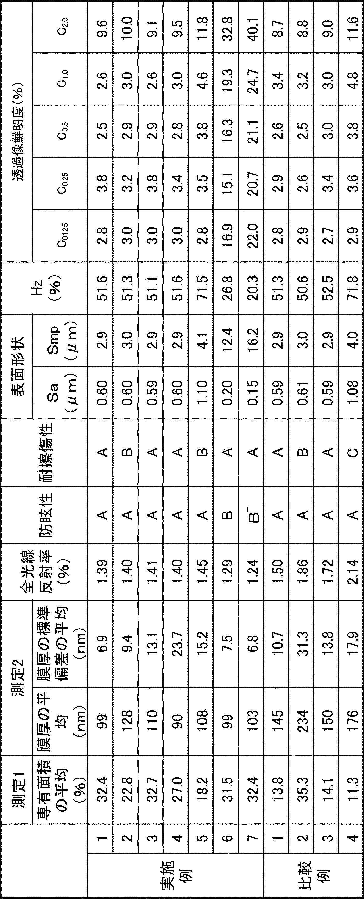
20:防眩層
30:低屈折率層
100:光学積層体
110:表示素子
120:画像表示パネル
Claims (17)
- 第1面と、前記第1面とは反対側の面である第2面とを有する光学積層体であって、
前記光学積層体は、前記第1面から前記第2面に向けて、低屈折率層及び防眩層をこの順に有し、
前記低屈折率層は、バインダー樹脂及び平均粒子径20nm以上の球状の粒子を含み、
前記第1面は凹凸形状を有し、
下記の測定1により算出した「平均粒子径20nm以上の球状の粒子の専有面積率の平均」が15.0%以上であり、
下記の測定2により算出した、「低屈折率層の膜厚の平均」が200nm以下であり、かつ、「低屈折率層の膜厚の標準偏差の平均」が25.0nm以下である、光学積層体。
<測定1>
(1-1)前記光学積層体の第1面側の表面を、走査電子顕微鏡により撮像する。撮像領域は、スケールバーを含まない領域が、横50.79μm×縦38.10μmとなるように調整する。さらに、横50.79μm×縦38.10μmの領域は、1280ピクセル×890ピクセルのピクセル数となるように調整する。
(1-2)上記(1-1)の横50.79μm×縦38.10μmの領域の画像を、最も暗い部分を0、最も明るい部分を255として、256階調に分ける。
上記(1-1)の横50.79μm×縦38.10μmの領域の画像を、「横10×縦10=100」の小領域に分割する。
100の小領域のうち、外周に位置する36の小領域を除いた64の小領域において、それぞれ、階調の標準偏差を算出する。64の小領域のうち、階調の標準偏差が最も大きい小領域を特定する。
64の小領域のうち、階調の標準偏差が最も大きい小領域を中心とした、「横3×縦3=9」の小領域を、低屈折率層の凸部及びその近傍領域とみなす。
(1-3)上記(1-2)の「凸部及びその近傍領域」を、さらに「横10×縦10=100」の微細領域に分割する。
100の微細領域において、それぞれ、階調の標準偏差を算出する。工程(1-3)の階調は、上記(1-2)の256階調を用いる。100の微細領域のうち、階調の標準偏差が最も大きい微細領域を特定する。
(1-4)上記(1-3)で特定した微細領域の中央部を中心として、横1270nm×縦890nmの領域の画像を、走査電子顕微鏡により撮像する。横1270nm×縦890nmの領域の画像中の低屈折率層を、低屈折率層の凸部とみなす。横1270nm×縦890nmの領域内における、平均粒子径20nm以上の球状の粒子が占める面積割合を算出する。
(1-5)前記光学積層体の第1面側の表面の20箇所において、上記(1-1)~(1-4)の作業を実施する。最小値及び最大値を除いた18箇所の面積割合の平均を、「平均粒子径20nm以上の球状の粒子の専有面積率の平均」とする。
<測定2>
(2-1)前記光学積層体の垂直断面を、走査型透過電子顕微鏡により撮像する。画像は、スケールバーを含まない領域が、横254μm×縦178μmとなるように調整する。
(2-2)上記(2-1)の横254μm×縦178μmの領域の画像において、低屈折率層の膜厚が最も厚い箇所を特定する。
(2-3)上記(2-2)で特定した箇所を中心として、横1270nm×縦890nmの領域の画像を、走査型透過電子顕微鏡により撮像する。横1270nm×縦890nmの領域の画像中の低屈折率層を、低屈折率層の凹部とみなす。横1270nm×縦890nmの領域内において、低屈折率層の膜厚、及び、低屈折率層の膜厚の標準偏差を算出する。低屈折率層の膜厚は、25箇所の膜厚の平均値とする。同様に、低屈折率層の膜厚の標準偏差は、25箇所の膜厚の標準偏差とする。前述した25箇所は、横1270nmの長さの範囲内において、50nm間隔で選択する。
(2-4)前記光学積層体の垂直断面の20箇所において、上記(2-1)~(2-3)の作業を実施する。最小値及び最大値を除いた18箇所の膜厚の平均及び膜厚の標準偏差の平均を、「低屈折率層の膜厚の平均」及び「低屈折率層の膜厚の標準偏差の平均」とする。 - 前記第1面は、三次元算術平均高さSaが0.30μm以上1.00μm以下である、請求項1に記載の光学積層体。
- 前記第1面は、前記第1面の三次元平均山間隔Smpが1.0μm以上10.0μm以下である、請求項1に記載の光学積層体。
- 前記低屈折率層が、微粒子の連結構造体を含む、請求項1に記載の光学積層体。
- 前記連結構造体は、長径の平均長さが20nm以上200nm以下である、請求項4に記載の光学積層体。
- 前記バインダー樹脂100質量部に対して、前記連結構造体を10質量部以上50質量部以下含む、請求項4又は5に記載の光学積層体。
- 前記低屈折率層が、前記バインダー樹脂として熱可塑性樹脂を含み、前記バインダー樹脂の全量に対して前記熱可塑性樹脂を60質量%以上含む、請求項1に記載の光学積層体。
- 前記低屈折率層が、前記バインダー樹脂として、さらに電離放射線硬化性樹脂組成物の硬化物を含む、請求項7に記載の光学積層体。
- 前記光学積層体は、前記第1面から前記第2面に向けて、前記低屈折率層、前記防眩層及び基材をこの順に有する、請求項1に記載の光学積層体。
- 前記防眩層が、バインダー樹脂及び粒子を含む、請求項1に記載の光学積層体。
- 前記防眩層の粒子として、平均粒子径1.0μm以上10.0μm以下の粒子を含む、請求項10に記載の光学積層体。
- 前記光学積層体は、下記の手法により測定される全光線反射率であるRSCIが1.50%未満である、請求項1に記載の光学積層体。
[全光線反射率(RSCI)の測定]
前記光学積層体の前記第2面側に、透明粘着剤を介して黒色板を貼り合わせたサンプルを作製する。前記サンプルの前記光学積層体側を光入射面として全光線反射率(RSCI)を測定する。 - JIS K7136:2000のヘイズが20%以上75%以下である、請求項1に記載の光学積層体。
- 偏光子と、前記偏光子の一方の側に配置された第一の透明保護板と、前記偏光子の他方の側に配置された第二の透明保護板とを有する偏光板であって、
前記第一の透明保護板及び前記第二の透明保護板の少なくとも一方が、請求項1に記載の光学積層体であり、前記光学積層体の前記第2面と前記偏光子とが対向して配置された、偏光板。 - 樹脂板又はガラス板上に保護フィルムを貼り合わせた画像表示装置用の表面板であって、前記保護フィルムが請求項1に記載の光学積層体であり、前記光学積層体の前記第2面と前記樹脂板又は前記ガラス板とが対向して配置された、画像表示装置用の表面板。
- 表示素子と、前記表示素子の光出射面側に配置された光学積層体を有する画像表示パネルであって、前記光学積層体として請求項1に記載の光学積層体を含む、画像表示パネル。
- 請求項16に記載の画像表示パネルを含む、画像表示装置。
Priority Applications (4)
| Application Number | Priority Date | Filing Date | Title |
|---|---|---|---|
| US19/159,928 US20260235791A1 (en) | 2023-03-02 | 2024-02-29 | Optical laminate and polarizing plate, surface plate, image display panel, and image display device using said optical laminate |
| CN202480013377.2A CN120712500A (zh) | 2023-03-02 | 2024-02-29 | 光学层叠体、以及使用了所述光学层叠体的偏光板、表面板、图像显示面板及图像显示装置 |
| JP2025503990A JPWO2024181533A1 (ja) | 2023-03-02 | 2024-02-29 | |
| KR1020257028586A KR20250153790A (ko) | 2023-03-02 | 2024-02-29 | 광학 적층체, 및 상기 광학 적층체를 사용한 편광판, 표면판, 화상 표시 패널 및 화상 표시 장치 |
Applications Claiming Priority (2)
| Application Number | Priority Date | Filing Date | Title |
|---|---|---|---|
| JP2023031727 | 2023-03-02 | ||
| JP2023-031727 | 2023-03-02 |
Publications (1)
| Publication Number | Publication Date |
|---|---|
| WO2024181533A1 true WO2024181533A1 (ja) | 2024-09-06 |
Family
ID=92589948
Family Applications (1)
| Application Number | Title | Priority Date | Filing Date |
|---|---|---|---|
| PCT/JP2024/007546 Ceased WO2024181533A1 (ja) | 2023-03-02 | 2024-02-29 | 光学積層体、並びに、前記光学積層体を用いた偏光板、表面板、画像表示パネル及び画像表示装置 |
Country Status (6)
| Country | Link |
|---|---|
| US (1) | US20260235791A1 (ja) |
| JP (1) | JPWO2024181533A1 (ja) |
| KR (1) | KR20250153790A (ja) |
| CN (1) | CN120712500A (ja) |
| TW (1) | TW202443198A (ja) |
| WO (1) | WO2024181533A1 (ja) |
Citations (7)
| Publication number | Priority date | Publication date | Assignee | Title |
|---|---|---|---|---|
| WO2008084604A1 (ja) * | 2007-01-12 | 2008-07-17 | Konica Minolta Opto, Inc. | 反射防止フィルム、反射防止フィルムの製造方法、偏光板及び表示装置 |
| JP2010143784A (ja) * | 2008-12-18 | 2010-07-01 | Adeka Corp | 分鎖状シリカ粒子よりなるシリカゾル及びその製造方法 |
| WO2015004811A1 (ja) * | 2013-07-12 | 2015-01-15 | 株式会社日立製作所 | 有機el素子及びそれを用いた有機el照明装置 |
| WO2015198762A1 (ja) * | 2014-06-27 | 2015-12-30 | コニカミノルタ株式会社 | 光学反射フィルム、光学反射フィルムの製造方法、およびそれを用いる光学反射体 |
| WO2016002434A1 (ja) * | 2014-06-30 | 2016-01-07 | 富士フイルム株式会社 | 液晶表示装置 |
| JP2016137611A (ja) * | 2015-01-27 | 2016-08-04 | 東レフィルム加工株式会社 | 透明積層フィルムおよびその製造方法 |
| JP2023009185A (ja) * | 2020-05-15 | 2023-01-19 | 大日本印刷株式会社 | 防眩フィルム及び画像表示装置 |
Family Cites Families (2)
| Publication number | Priority date | Publication date | Assignee | Title |
|---|---|---|---|---|
| JP2010008757A (ja) | 2008-06-27 | 2010-01-14 | Konica Minolta Opto Inc | 防眩性反射防止フィルム、偏光板及び画像表示装置 |
| JP2020122926A (ja) | 2019-01-31 | 2020-08-13 | Jnc株式会社 | 防眩性反射防止ハードコートフィルム、画像表示装置、および防眩性反射防止ハードコートフィルムの製造方法 |
-
2024
- 2024-02-29 TW TW113107275A patent/TW202443198A/zh unknown
- 2024-02-29 WO PCT/JP2024/007546 patent/WO2024181533A1/ja not_active Ceased
- 2024-02-29 JP JP2025503990A patent/JPWO2024181533A1/ja active Pending
- 2024-02-29 KR KR1020257028586A patent/KR20250153790A/ko active Pending
- 2024-02-29 US US19/159,928 patent/US20260235791A1/en active Pending
- 2024-02-29 CN CN202480013377.2A patent/CN120712500A/zh active Pending
Patent Citations (7)
| Publication number | Priority date | Publication date | Assignee | Title |
|---|---|---|---|---|
| WO2008084604A1 (ja) * | 2007-01-12 | 2008-07-17 | Konica Minolta Opto, Inc. | 反射防止フィルム、反射防止フィルムの製造方法、偏光板及び表示装置 |
| JP2010143784A (ja) * | 2008-12-18 | 2010-07-01 | Adeka Corp | 分鎖状シリカ粒子よりなるシリカゾル及びその製造方法 |
| WO2015004811A1 (ja) * | 2013-07-12 | 2015-01-15 | 株式会社日立製作所 | 有機el素子及びそれを用いた有機el照明装置 |
| WO2015198762A1 (ja) * | 2014-06-27 | 2015-12-30 | コニカミノルタ株式会社 | 光学反射フィルム、光学反射フィルムの製造方法、およびそれを用いる光学反射体 |
| WO2016002434A1 (ja) * | 2014-06-30 | 2016-01-07 | 富士フイルム株式会社 | 液晶表示装置 |
| JP2016137611A (ja) * | 2015-01-27 | 2016-08-04 | 東レフィルム加工株式会社 | 透明積層フィルムおよびその製造方法 |
| JP2023009185A (ja) * | 2020-05-15 | 2023-01-19 | 大日本印刷株式会社 | 防眩フィルム及び画像表示装置 |
Also Published As
| Publication number | Publication date |
|---|---|
| JPWO2024181533A1 (ja) | 2024-09-06 |
| US20260235791A1 (en) | 2026-08-13 |
| TW202443198A (zh) | 2024-11-01 |
| CN120712500A (zh) | 2025-09-26 |
| KR20250153790A (ko) | 2025-10-27 |
Similar Documents
| Publication | Publication Date | Title |
|---|---|---|
| CN104915050B (zh) | 触摸面板、显示装置和光学片、以及光学片的筛选方法和光学片的制造方法 | |
| CN116699738B (zh) | 防眩膜和图像显示装置 | |
| JP7564375B2 (ja) | 防眩フィルム、並びに、それを用いた偏光板、表面板、画像表示パネル及び画像表示装置 | |
| JP7601134B2 (ja) | 防眩フィルム及び画像表示装置 | |
| WO2019065865A1 (ja) | 防眩フィルム及びそれを用いた表示装置 | |
| US12130408B2 (en) | Anti-glare film; anti-glare article, touchscreen, and display device using same; and method for selecting anti-glare film | |
| JP7681552B2 (ja) | 防眩フィルム及び画像表示装置 | |
| JP7816405B2 (ja) | 防眩フィルム及び画像表示装置 | |
| WO2023210620A1 (ja) | 光学フィルム、画像表示パネル及び画像表示装置 | |
| JP7409574B1 (ja) | 光学フィルム、画像表示パネル及び画像表示装置 | |
| JP2024052542A (ja) | 光学フィルム、並びに、前記光学フィルムを用いた偏光板、表面板、画像表示パネル及び画像表示装置、並びに、前記光学フィルムの製造方法、並びに、光学フィルムの選定方法、並びに、指紋拭き取り性の評価方法 | |
| JP7343023B1 (ja) | 光学フィルム、並びに、前記光学フィルムを用いた偏光板、表面板、画像表示パネル及び画像表示装置、並びに、前記光学フィルムの製造方法、並びに、光学フィルムの選定方法 | |
| WO2024070996A1 (ja) | 光学フィルム、並びに、前記光学フィルムを用いた偏光板、表面板、画像表示パネル及び画像表示装置、並びに、前記光学フィルムの製造方法、並びに、光学フィルムの選定方法、並びに、指紋拭き取り性の評価方法 | |
| JP6484846B2 (ja) | タッチパネル、表示装置及び光学シート、並びに光学シートの選別方法及び光学シートの製造方法 | |
| KR20250153790A (ko) | 광학 적층체, 및 상기 광학 적층체를 사용한 편광판, 표면판, 화상 표시 패널 및 화상 표시 장치 | |
| TW202328708A (zh) | 防眩膜、以及使用其之偏光板、表面板、影像顯示面板及影像顯示裝置 |
Legal Events
| Date | Code | Title | Description |
|---|---|---|---|
| 121 | Ep: the epo has been informed by wipo that ep was designated in this application |
Ref document number: 24764010 Country of ref document: EP Kind code of ref document: A1 |
|
| WWE | Wipo information: entry into national phase |
Ref document number: 2025503990 Country of ref document: JP |
|
| ENP | Entry into the national phase |
Ref document number: 1020257028586 Country of ref document: KR Free format text: ST27 STATUS EVENT CODE: A-0-1-A10-A15-NAP-PA0105 (AS PROVIDED BY THE NATIONAL OFFICE) |
|
| WWE | Wipo information: entry into national phase |
Ref document number: 202517081153 Country of ref document: IN |
|
| WWP | Wipo information: published in national office |
Ref document number: 202517081153 Country of ref document: IN |
|
| NENP | Non-entry into the national phase |
Ref country code: DE |
|
| WWP | Wipo information: published in national office |
Ref document number: 1020257028586 Country of ref document: KR |
|
| 122 | Ep: pct application non-entry in european phase |
Ref document number: 24764010 Country of ref document: EP Kind code of ref document: A1 |