WO2024180751A1 - 電流センサ回路 - Google Patents
電流センサ回路 Download PDFInfo
- Publication number
- WO2024180751A1 WO2024180751A1 PCT/JP2023/007734 JP2023007734W WO2024180751A1 WO 2024180751 A1 WO2024180751 A1 WO 2024180751A1 JP 2023007734 W JP2023007734 W JP 2023007734W WO 2024180751 A1 WO2024180751 A1 WO 2024180751A1
- Authority
- WO
- WIPO (PCT)
- Prior art keywords
- circuit
- signal
- detection
- current
- detection coil
- Prior art date
- Legal status (The legal status is an assumption and is not a legal conclusion. Google has not performed a legal analysis and makes no representation as to the accuracy of the status listed.)
- Ceased
Links
Images





Classifications
-
- G—PHYSICS
- G01—MEASURING; TESTING
- G01R—MEASURING ELECTRIC VARIABLES; MEASURING MAGNETIC VARIABLES
- G01R15/00—Details of measuring arrangements of the types provided for in groups G01R17/00 - G01R29/00, G01R33/00 - G01R33/26 or G01R35/00
- G01R15/14—Adaptations providing voltage or current isolation, e.g. for high-voltage or high-current networks
- G01R15/18—Adaptations providing voltage or current isolation, e.g. for high-voltage or high-current networks using inductive devices, e.g. transformers
-
- G—PHYSICS
- G01—MEASURING; TESTING
- G01R—MEASURING ELECTRIC VARIABLES; MEASURING MAGNETIC VARIABLES
- G01R15/00—Details of measuring arrangements of the types provided for in groups G01R17/00 - G01R29/00, G01R33/00 - G01R33/26 or G01R35/00
- G01R15/14—Adaptations providing voltage or current isolation, e.g. for high-voltage or high-current networks
- G01R15/18—Adaptations providing voltage or current isolation, e.g. for high-voltage or high-current networks using inductive devices, e.g. transformers
- G01R15/183—Adaptations providing voltage or current isolation, e.g. for high-voltage or high-current networks using inductive devices, e.g. transformers using transformers with a magnetic core
- G01R15/185—Adaptations providing voltage or current isolation, e.g. for high-voltage or high-current networks using inductive devices, e.g. transformers using transformers with a magnetic core with compensation or feedback windings or interacting coils, e.g. 0-flux sensors
-
- G—PHYSICS
- G01—MEASURING; TESTING
- G01R—MEASURING ELECTRIC VARIABLES; MEASURING MAGNETIC VARIABLES
- G01R19/00—Arrangements for measuring currents or voltages or for indicating presence or sign thereof
-
- G—PHYSICS
- G01—MEASURING; TESTING
- G01R—MEASURING ELECTRIC VARIABLES; MEASURING MAGNETIC VARIABLES
- G01R19/00—Arrangements for measuring currents or voltages or for indicating presence or sign thereof
- G01R19/0092—Measuring current only
Definitions
- the present invention relates to a current sensor circuit that detects direct current.
- Patent Document 1 discloses a current sensor capable of measuring the direction of a current to be detected without using a Hall element.
- This current sensor includes a magnetic core for passing magnetic flux due to the current to be detected, a resonant circuit including a winding wound around the magnetic core, an oscillator for applying a signal of a predetermined frequency to the resonant circuit, an output circuit connected to the resonant circuit and outputting an electric signal corresponding to the direction of the current to be detected based on a characteristic change of the resonant circuit that changes according to the direction of the current to be detected, and a magnetic field bias unit for applying a magnetic field bias to the magnetic core.
- the present invention provides a current sensor circuit technology capable of suppressing the effects of noise and detecting DC current with high accuracy.
- a current sensor circuit capable of detecting a direct current flowing through a conductor to be detected, comprising: a detection coil configured such that its inductance changes with the direct current; a resonant capacitor that forms a series resonant circuit together with the detection coil; a phase adjustment circuit that receives a feedback signal from the resonant capacitor and outputs a drive signal; a switching circuit that includes a plurality of switching elements forming a half-bridge circuit or a full-bridge circuit and supplies an alternating current signal to the detection coil and the resonant capacitor by switching the plurality of switching elements in accordance with the pulse period of the drive signal; a signal conversion circuit that converts the drive signal output from the phase adjustment circuit into a detection signal indicating a change in the direct current; and a detection terminal that outputs the detection signal to the outside, and the phase adjustment circuit sets the pulse period of the drive signal in accordance with the phase difference between the feedback signal and the drive signal so that the frequency of the alternating current signal flowing through
- the above aspect provides a current sensor circuit technology that can detect DC current with high accuracy while suppressing the effects of noise.
- FIG. 2 is a circuit diagram of a current sensor circuit according to the embodiment
- FIG. 3 is a diagram conceptually illustrating an example of the configuration of a detection coil in the present embodiment.
- FIG. 1 is an example of a circuit diagram of a pulse conversion circuit.
- 6 is a graph showing the relationship between the inductance change of the detection coil, the pulse frequency change of the drive signal, and the DC bias current.
- 4A to 4D are diagrams showing signal waveforms at points A, B, C, and D of the current sensor circuit in this embodiment.
- 13 is a diagram conceptually showing a configuration of a detection coil in a modified example.
- FIG. FIG. 11 is a circuit diagram of a current sensor circuit according to a modified example.
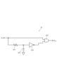
- FIG. 1 is a circuit diagram of a current sensor circuit 1 according to the present embodiment.
- the current sensor circuit 1 includes a phase adjustment circuit 10, a switching circuit 20, a detection circuit 30, a feedback rectifier circuit 40, a signal conversion circuit 50, a detection terminal 60, a magnetic field bias section, and the like.
- the detection circuit 30 is composed of a resistor element R1, a detection coil N1, and a resonant capacitor C1, which are connected in series, and therefore becomes a series resonant circuit when an AC signal of a resonant frequency flows through the detection circuit 30.
- the detection coil N1 is configured such that its inductance changes when a direct current (sometimes referred to as a detected current) flows through a detected conductor of a measured system.
- FIG. 2 is a diagram conceptually showing an example of the configuration of the detection coil N1 in this embodiment. 2, the winding of the detection coil N1 is wound around a magnetic core 32 through which the detected conductor TL is inserted.
- a direct current I flows through the detected conductor TL
- a magnetic field is generated around the detected conductor TL, which changes the magnetic flux in the magnetic core 32.
- This change in magnetic flux changes the inductance of the detection coil N1, which has a winding wound around the magnetic core 32.
- the magnetic core 32 exhibits such an effect, its material is not limited and may be ferrite, electromagnetic steel sheet, or the like.
- the magnetic core 32 illustrated in FIG. 2 is a ring-shaped core called a toroidal core, with the detected conductor TL passing through its center, but this configuration is not limited as long as it achieves the above-mentioned effect.
- bias coil N2 is also wound around the magnetic core 32.
- the bias coil N2 constitutes a magnetic field bias section and applies a magnetic field bias capable of causing the magnetic core 32 to reach a magnetic saturation region.
- the magnetic field bias section will be described in detail later.
- the inductance of the detection coil N1 becomes small, whereas when the current to be detected I flows in a direction that generates a magnetic flux in the opposite direction (cancelling direction) to the magnetic flux in the magnetic core 32 generated by the DC bias current Ib flowing through the bias coil N2, the inductance of the detection coil N1 becomes large.
- the direction of the detected current I in which the inductance of the detection coil N1 decreases is defined as a positive direction (+I)
- the direction of the detected current I in which the inductance of the detection coil N1 increases is defined as a negative direction (-I).
- the switching circuit 20 includes a drive circuit 22, two transistors Q1 and Q2, and the like.
- the transistors Q1 and Q2 are FETs (Field Effect Transistors) and can be referred to as switching elements.
- transistors Q1 and Q2 are N-channel metal oxide semiconductor field effect transistors (MOSFETs) that form a half-bridge circuit, and a detection circuit 30 is connected between the source and drain of transistor Q2.
- MOSFETs metal oxide semiconductor field effect transistors
- the drive circuit 22 is connected to the transistors Q1 and Q2 so as to be able to apply a gate-source voltage (hereinafter, sometimes referred to as a VGS voltage) to the transistors Q1 and Q2.
- the drive circuit 22 alternately applies a VGS voltage exceeding a threshold voltage to the transistors Q1 and Q2, thereby alternately switching the on-off states of the transistors Q1 and Q2 (performing a switching operation).
- the drive circuit 22 switches the on-off states of the transistors Q1 and Q2 in accordance with the pulse period of the drive signal from the phase adjustment circuit 10.
- an AC signal having a frequency corresponding to the period of the drive signal from the phase adjustment circuit 10 flows in the detection circuit 30.
- the pulse period of the drive signal from the phase adjustment circuit 10 is controlled so that an AC signal of a resonant frequency flows in the detection circuit 30.
- the feedback rectifier circuit 40 is a circuit that half-wave rectifies the feedback signal from the detection circuit 30. Specifically, the feedback rectifier circuit 40 half-wave rectifies the AC voltage waveform applied to the resonant capacitor C1, and sends the half-wave rectified voltage waveform to the phase adjustment circuit 10.
- the phase adjustment circuit 10 receives a feedback signal from the detection circuit 30 and outputs a drive signal. Specifically, the phase adjustment circuit 10 sets the pulse period of the drive signal to be output so that the frequency of the AC signal flowing through the detection circuit 30 follows the resonant frequency of the detection circuit 30 (series resonant circuit) according to the phase difference between the drive signal and a signal (feedback signal) that is a half-wave rectified AC voltage waveform applied to the resonant capacitor C1.
- the phase adjustment circuit 10 includes a feedback pulse generation circuit 11, a PLL (Phase Locked Loop) circuit 16, and the like.
- the feedback pulse generating circuit 11 includes a NOT circuit 12, a variable resistance element 13, a capacitor 14, etc.
- the NOT circuit 12 converts the half-wave rectified waveform from the feedback rectifying circuit 40 into a pulse waveform using a threshold voltage, and an RC filter formed by the variable resistance element 13 and the capacitor 14 corrects the deviation when the pulse waveform is shaped. In this way, the feedback pulse signal (SIG pulse) converted by the feedback pulse generating circuit 11 from the half-wave rectified waveform from the feedback rectifying circuit 40 is sent to the PLL circuit 16.
- the PLL circuit 16 compares the phase of the feedback pulse signal (SIG pulse) sent from the feedback pulse generating circuit 11 with the drive signal (REF pulse), and adjusts the pulse period of the output signal, the drive signal (PLLout), so that the phase difference is eliminated.
- the PLL circuit 16 only needs to have the configuration of a known single-loop PLL circuit, and is composed of, for example, a frequency divider, a phase comparator, a filter, and a voltage controlled oscillator (VCO (Voltage Controlled Oscillator)).
- VCO Voltage Controlled Oscillator
- the signal conversion circuit 50 converts the drive signal output from the phase adjustment circuit 10 into a detection signal that indicates a change in the DC current flowing through the detected conductor TL. This detection signal is output to the outside from a detection terminal DCSIG.
- the signal conversion circuit 50 includes a pulse conversion circuit 51, a resistive element 52, a capacitor 53, etc.
- the pulse conversion circuit 51 converts the drive signal output from the phase adjustment circuit 10 into a pulse frequency modulation (PFM) signal.
- PFM pulse frequency modulation
- the resistive element 52 and the capacitor 53 form an RC filter, and smooth the PFM signal output from the pulse conversion circuit 51 to a voltage level waveform. This voltage level waveform becomes a detection signal indicating a change in the DC current flowing through the detected conductor TL.
- FIG. 3 is an example of a circuit diagram of the pulse conversion circuit 51.
- the pulse conversion circuit 51 is a monostable multivibrator circuit composed of a resistive element 511, a capacitor 512, a NOT circuit 513, an AND circuit 514, etc.
- the rising timing of the pulse of the input drive signal is shifted by the resistive element 511 and the capacitor 512, and the signal inverted by the NOT circuit 513 and the input drive signal are input to the AND circuit 514, whereby a PFM signal having a constant pulse width and a duty ratio that changes in proportion to the pulse period of the drive signal is output.
- the configuration of the pulse conversion circuit 51 is not limited to the example configuration shown in FIG. 3, and it may be a monostable multivibrator circuit having another configuration.
- the magnetic field bias section includes the bias coil N2 (see FIG. 2) described above and a DC power supply (not shown) that passes a constant current through the bias coil N2.
- This DC power supply supplies DC power (+5V in the example of FIG. 1) to the bias coil N2, which has a winding wound around the magnetic core 32, thereby applying a magnetic field bias to the magnetic core 32 and causing it to reach a magnetic saturation region.
- This causes the inductance characteristic of the detection coil N1, which has a winding wound around the same magnetic core 32, to transition to a region where the inductance changes linearly.
- FIG. 4 is a graph showing the relationship between the inductance change of the detection coil N1, the pulse frequency change of the drive signal, and the DC bias current Ib.
- the horizontal axis of FIG. 4 represents the detected current I
- the vertical axis of FIG. 4 represents the pulse frequency of the drive signal (the reciprocal of the pulse period). 2
- the inductance of the detection coil N1 changes depending on the current I to be detected. As shown in FIG. 4, when the positive current I to be detected increases, the inductance of the detection coil N1 decreases, and when the negative current I to be detected increases, the inductance of the detection coil N1 increases.
- the resonant frequency of the detection circuit 30 increases, and the pulse frequency of the drive signal also increases accordingly (the pulse period becomes shorter).
- the resonant frequency of the detection circuit 30 decreases, and the pulse frequency of the drive signal also decreases accordingly (the pulse period becomes longer).
- the inductance change of the detection coil N1 is not a completely linear change. Therefore, in this embodiment, the winding of the bias coil N2 is wound around the magnetic core 32 together with the detection coil N1, and a DC bias current is passed through the bias coil N2, thereby canceling the nonlinear region in the inductance characteristic of the detection coil N1 and shifting it to a linear region.
- the output of the DC power supply of the magnetic field bias section is set so that the inductance of the detection coil N1 changes in a linear region within the measurable range (from -Imax to +Imax) of the detected current I, and the inductance value of the detection coil N1 when the detected current I is not flowing (zero amperes) is the median of that linear change region.
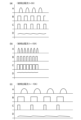
- Fig. 5 is a diagram showing signal waveforms at points A, B, C, and D of the current sensor circuit 1 in this embodiment. The positions of points A, B, C, and D are as shown in Fig. 1.
- Fig. 5(a) shows the signal waveform when the current I to be detected is not flowing (when it is 0 (A))
- Fig. 5(b) shows the signal waveform when the current I to be detected is +10 (A)
- Fig. 5(c) shows the signal waveform when the current I to be detected is -10 (A).
- the switching circuit 20 When no current flows through the detected conductor TL ( Figure 5 (a)), the switching circuit 20 performs switching operation of the transistors Q1 and Q2 in accordance with the pulse period of the drive signal output from the phase adjustment circuit 10 so that the detection circuit 30 is in a resonant state.
- the AC voltage waveform (basic signal) applied to the resonant capacitor C1 of the detection circuit 30 is a resonant frequency waveform, and this waveform signal is half-wave rectified by the feedback rectifier circuit 40.
- the waveform at point A in FIG. 5(a) is the half-wave rectified waveform output from the feedback rectifier circuit 40.
- Such a basic signal (half-wave rectified waveform) is converted to a pulse waveform at a threshold voltage in the feedback pulse generating circuit 11 of the phase adjustment circuit 10, and further subjected to deviation correction, and is sent as a feedback pulse signal to the PLL circuit 16.
- the PLL circuit 16 compares the phase of this feedback pulse signal with that of the drive signal, and adjusts the pulse period of the drive signal (PLLout), which is an output signal, so that the phase difference is eliminated.
- the waveform at point B in FIG. 5(a) is the waveform of the drive signal output from the phase adjustment circuit 10. At this time, since no current flows through the detected conductor TL, there is basically no phase difference, and the pulse period of the drive signal is maintained so as to correspond to the resonant frequency of the detection circuit 30.
- the drive signal is sent to the switching circuit 20 and also to the signal conversion circuit 50, where it is converted into a PFM signal in the pulse conversion circuit 51.
- the waveform at point C in Fig. 5(a) is the waveform of this PFM signal.
- This PFM signal is smoothed by an RC filter of a resistor element 52 and a capacitor 53 in the signal conversion circuit 50 to form a voltage level waveform, which can be output from the detection terminal DCSIG to the outside.
- the waveform at point D in Figure 5(a) is this voltage level waveform, and indicates the voltage level corresponding to the detected current I being 0 (A).
- the switching circuit 20 performs switching operations of the transistors Q1 and Q2 so as to correspond to the pulse period of the drive signal adjusted in this manner, so that the frequency of the AC signal flowing through the detection circuit 30 follows the resonant frequency of the detection circuit 30 which changes in response to the decrease in inductance of the detection coil N1.
- the drive signal adjusted in this way is converted to a PFM signal in the pulse conversion circuit 51 (waveform at point C in FIG. 5(b)), and this PFM signal is smoothed by the RC filter of the resistor element 52 and capacitor 53 in the signal conversion circuit 50 to form a voltage level waveform (waveform at point D in FIG. 5(b)).
- This voltage level waveform indicates a voltage level corresponding to the detected current I being +10 (A).
- the switching circuit 20 performs switching operations of the transistors Q1 and Q2 so as to correspond to the pulse period of the drive signal adjusted in this manner, so that the frequency of the AC signal flowing through the detection circuit 30 follows the resonant frequency of the detection circuit 30 which changes in response to the increase in inductance of the detection coil N1.
- the drive signal adjusted in this way is converted to a PFM signal in the pulse conversion circuit 51 (waveform at point C in FIG. 5(c)), and this PFM signal is smoothed by the RC filter of the resistor element 52 and capacitor 53 in the signal conversion circuit 50 to form a voltage level waveform (waveform at point D in FIG. 5(c)).
- This voltage level waveform shows a voltage level corresponding to the detected current I being -10 (A).
- the magnitude of the current I to be detected is captured by the change in inductance of the detection coil N1 and the change in the resonant frequency of the detection circuit 30, and this resonant frequency is tracked by the phase adjustment circuit 10, and a detection signal is generated from the drive signal output from the phase adjustment circuit 10.
- the circuit is operated to follow the resonant frequency of the detection circuit 30, so that it is possible to suppress the reaction to external noise frequencies.
- the detection signal is obtained from the PFM signal corresponding to the pulse duty, thereby improving noise resistance. Therefore, according to this embodiment, it is possible to maintain the detection level of DC current with high accuracy while being less susceptible to the effects of noise.
- a nonlinear change region exists in the inductance characteristics of the detection coil N1, but by winding the windings of the bias coil N2 around the magnetic core 32 around which the windings of the detection coil N1 are wound and passing a DC bias current Ib, this nonlinear change region is canceled and the inductance of the detection coil N1 is changed in a linear change region. This makes it possible to detect the magnitude of the target current I with high accuracy.
- the PFM signal output from the pulse conversion circuit 51 is a signal whose pulse width is constant regardless of the pulse period of the drive signal while being synchronized with the rising timing of the pulse of the drive signal (waveform at point B). That is, the drive signal output from the phase adjustment circuit 10 is a signal whose duty ratio is constant and whose pulse width is proportional to the pulse period (pulse frequency), whereas the PFM signal is a signal whose pulse width is constant and whose duty ratio is proportional to the pulse period (pulse frequency).
- the smoothed signal By converting the smoothed signal into such a PFM signal, the signal can be made into a signal whose level rises and falls according to the pulse period (pulse frequency), and can be made into a detection signal that indicates changes in the current I to be detected.
- the current sensor circuit 1 may not have a magnetic bias unit if it is possible to detect whether a direct current flows through the detection target conductor TL or whether a direct current exceeding a predetermined current value flows through the detection target conductor TL at a detection current level at which an inductance change occurs in the detection coil N1.
- the signal conversion circuit 50 is not limited to the above configuration as long as it can convert the drive signal output from the phase adjustment circuit 10 into a detection signal that can indicate a change in the detection target current.
- the signal conversion circuit 50 may generate a detection signal without converting it into a PFM signal.
- the magnetic bias unit includes the bias coil N2 and the DC power supply, but the magnetic bias unit may include a bias magnet.
- the bias coil N2 and the DC power supply (+5V) are not required.
- FIG. 6 is a diagram conceptually showing the configuration of a detection coil N1 in a modified example. Similar to the above-described embodiment, the magnetic core 32 is wound with the windings of the detection coil N1 and has the detected conductor TL inserted therethrough, but in this modification, there is no winding of the bias coil N2, and instead a bias magnet BM is provided in the magnetic core 32.
- the magnetic core 32 is formed in a C-shape with a portion of the annular shape interrupted, and the bias magnet BM is fitted into the interrupted gap to form an annular body as a whole.
- the bias magnet BM applies a magnetic field bias capable of reaching a magnetic saturation region to the magnetic core 32. That is, the bias magnet BM has a magnetic force capable of shifting the inductance characteristic of the detection coil N1 to a region where the inductance changes linearly (linear change region). Even if the magnetic bias section has such a configuration, the same effects as those of the above-described embodiment can be obtained.
- FIG. 7 is a circuit diagram of the current sensor circuit 1 according to a modified example.
- the switching circuit 20 described above can be modified to include multiple transistors Q1, Q2, Q3 and Q4 forming a full bridge circuit.
- the drive circuit 22 is connected to the transistors Q1, Q2, Q3, and Q4 so as to be able to apply a gate-source voltage ( VGS voltage) to the transistors Q1, Q2, Q3, and Q4.
- VGS voltage gate-source voltage
- the drive circuit 22 alternately applies a VGS voltage exceeding a threshold voltage to the pair of transistors Q1 and Q4 and the pair of transistors Q2 and Q3 in accordance with the pulse period of the drive signal from the phase adjustment circuit 10, thereby alternately switching the on/off states of the pair of transistors Q1 and Q4 and the pair of transistors Q2 and Q3 (performing a switching operation).
- This allows an AC signal having a frequency corresponding to the pulse period of the drive signal from the phase adjustment circuit 10 to flow through the detection circuit 30, similar to the above-described embodiment.
- a current sensor circuit capable of detecting a direct current flowing through a conductor to be detected, A detection coil configured such that an inductance changes with the direct current; a resonant capacitor that configures a series resonant circuit together with the detection coil; a phase adjustment circuit that receives a feedback signal from the resonant capacitor and outputs a drive signal; a switching circuit including a plurality of switching elements forming a half-bridge circuit or a full-bridge circuit, the switching circuit supplying an AC signal to the detection coil and the resonant capacitor by switching the plurality of switching elements in response to a pulse period of the drive signal; a signal conversion circuit that converts the drive signal output from the phase adjustment circuit into a detection signal that indicates a change in the DC current; a detection terminal for outputting the detection signal to an outside; Equipped with the phase adjustment circuit sets a pulse period of the drive signal in accordance with a phase difference between the feedback signal and the drive signal so that a frequency of the AC signal flowing through the detection coil and the resonance
- the signal conversion circuit includes a pulse conversion circuit that converts the drive signal output from the phase adjustment circuit into a PFM (pulse frequency modulation) signal, and obtains the detection signal indicating the magnitude of the DC current by a voltage magnitude from the PFM signal;
- PFM pulse frequency modulation
- ⁇ 3> a magnetic core around which the detection coil is wound and through which the detected conductor is inserted;
Landscapes
- Physics & Mathematics (AREA)
- General Physics & Mathematics (AREA)
- Engineering & Computer Science (AREA)
- Power Engineering (AREA)
- Measurement Of Current Or Voltage (AREA)
- Measuring Magnetic Variables (AREA)
Abstract
Description
下記特許文献1には、ホール素子を使用せずに被検出電流の向きを測定可能な電流センサが開示されている。この電流センサは、被検出電流による磁束を通すための磁性体コアと、磁性体コアに巻回された巻線を含む共振回路と、その共振回路に対して所定の周波数の信号を印加する発振器と、その共振回路に接続され、被検出電流の向きに応じて変化する共振回路の特性変化に基づいて被検出電流の向きに対応する電気信号を出力する出力回路と、磁性体コアに磁界バイアスを印加する磁界バイアス部とを備える。
本発明は、ノイズの影響を抑え高精度に直流電流を検出可能な電流センサ回路技術を提供する。
図1は、本実施形態における電流センサ回路1の回路図である。
電流センサ回路1は、位相調整回路10、スイッチング回路20、検出回路30、帰還整流回路40、信号変換回路50、検出端子60、磁界バイアス部等を有している。
検出コイルN1は、被測定系の被検出導線に直流電流(被検出電流と表記する場合もある)が流れることでそのインダクタンスが変化するよう構成されている。
図2に示されるように、検出コイルN1の巻線は被検出導線TLが挿通された磁気コア32に巻回されている。このような構成により、被検出導線TLに直流電流Iが流れることでその被検出導線TLの周囲に発生した磁界によって磁気コア32内の磁束が変化し、この磁束の変化に伴い磁気コア32に巻線が巻回されている検出コイルN1のインダクタンスが変化する。
また、図2に例示される磁気コア32は、トロイダルコアと呼ばれる環状のコアであり、その中心に被検出導線TLが挿通されているが、上述のような作用を奏するのであれば、このような構成も限定されない。
被検出電流Iがバイアス用コイルN2に流れる直流バイアス電流Ibによって生じる磁気コア32内の磁束と同方向(重なり合う方向)の磁束を生じさせる向きに流れる場合には、検出コイルN1のインダクタンスは小さくなるのに対して、被検出電流Iがバイアス用コイルN2に流れる直流バイアス電流Ibによって生じる磁気コア32内の磁束と逆方向(打消し合う方向)の磁束を生じさせる向きに流れる場合には、検出コイルN1のインダクタンスは大きくなる。
本実施形態では、検出コイルN1のインダクタンスが小さくなる被検出電流Iの向きを正の向き(+I)とし、検出コイルN1のインダクタンスが大きくなる被検出電流Iの向きを負の向き(-I)とする。
本実施形態におけるトランジスタQ1及びQ2は、FET(Field Effect Transistor)であり、スイッチング素子と表記できる。
図1の例においてトランジスタQ1及びQ2は、Nチャンネル型のMOSFET(Metal Oxide Semiconductor Field Effect Transistor)であり、ハーフブリッジ回路を形成している。そして、トランジスタQ2のソース-ドレイン間に検出回路30が接続されている。
ドライブ回路22は、トランジスタQ1及びトランジスタQ2に対して交互に閾値電圧を超えるVGS電圧を印加することで、トランジスタQ1及びトランジスタQ2のオンオフ状態を交互にスイッチングさせる(スイッチング動作させる)。このとき、ドライブ回路22は、位相調整回路10からのドライブ信号のパルス周期に合わせてトランジスタQ1及びQ2のオンオフ状態をスイッチングさせる。これにより、検出回路30には、位相調整回路10からのドライブ信号の周期に対応する周波数の交流信号が流れる。詳細は後述するが、位相調整回路10からのドライブ信号のパルス周期は、検出回路30に共振周波数の交流信号が流れるように制御される。
帰還パルス生成回路11は、NOT回路12、可変抵抗素子13、コンデンサ14等を含む。NOT回路12は、帰還整流回路40からの半波整流波形を閾値電圧でパルス波形に変換し、可変抵抗素子13及びコンデンサ14で形成されるRCフィルタがそのパルス波形の成形時のずれを補正する。このようにして帰還整流回路40からの半波整流波形から帰還パルス生成回路11で変換された帰還パルス信号(SIGパルス)がPLL回路16に送られる。
信号変換回路50は、パルス変換回路51、抵抗素子52、コンデンサ53等を含む。パルス変換回路51は、位相調整回路10から出力されるドライブ信号をパルス周波数変調(PFM(Pulse Frequency Modulation))信号に変換する。抵抗素子52及びコンデンサ53は、RCフィルタを形成し、パルス変換回路51から出力されるPFM信号を平滑化することで電圧レベル波形とする。この電圧レベル波形が被検出導線TLに流れる直流電流の変化を示す検出信号となる。
図3の例においてパルス変換回路51は、抵抗素子511、コンデンサ512、NOT回路513、AND回路514等から構成される単安定マルチバイブレータ回路である。パルス変換回路51では、入力されたドライブ信号のパルスの立ち上がりタイミングが抵抗素子511とコンデンサ512とによりずらされNOT回路513で反転された信号と、入力されたドライブ信号とが、AND回路514に入力されることで、パルス幅が一定でデューティー比が当該ドライブ信号のパルス周期に比例変化するPFM信号が出力される。
但し、パルス変換回路51の構成は、図3に示される構成例に限定されず、他の構成を有する単安定マルチバイブレータ回路であってもよい。
図2で例示される構成により被検出電流Iによって検出コイルN1のインダクタンスが変化する。図4に示されるように、正の向きの被検出電流Iが大きくなると、検出コイルN1のインダクタンスは小さくなり、負の向きの被検出電流Iが大きくなると、検出コイルN1のインダクタンスは大きくなる。そして、検出コイルN1のインダクタンスが小さくなると、検出回路30の共振周波数は高くなることから、これに追従してドライブ信号のパルス周波数も高くなる(パルス周期が短くなる)。また、検出コイルN1のインダクタンスが大きくなると、検出回路30の共振周波数は低くなることから、これに追従してドライブ信号のパルス周波数も低くなる(パルス周期が長くなる)。
このため磁界バイアス部の直流電源の出力は、被検出電流Iの測定可能範囲(-Imaxから+Imaxの範囲)内において検出コイルN1のインダクタンスが線形領域で変化し、かつ被検出電流Iが流れていない(ゼロアンペア)ときの検出コイルN1のインダクタンス値がその線形変化領域の中央値となるように設定される。
次に、図5を用いて、上述のような回路構成を有する電流センサ回路1の動作を説明する。図5は、本実施形態における電流センサ回路1のA点、B点、C点及びD点での信号波形を示す図である。A点、B点、C点及びD点の各位置は、図1に示されるとおりである。また、図5(a)は、被検出電流Iが流れていないとき(0(A)のとき)の信号波形を示し、図5(b)は、被検出電流Iが+10(A)のときの信号波形を示し、図5(c)は、被検出電流Iが-10(A)のときの信号波形を示している。
このとき検出回路30の共振コンデンサC1にかかる交流電圧波形(基幹信号)は共振周波数波形となっており、この波形信号が帰還整流回路40により半波整流される。図5(a)のA点波形が帰還整流回路40から出力される半波整流波形である。
このとき被検出導線TLに電流が流れていないことから基本的には当該位相差はなく、ドライブ信号のパルス周期は検出回路30の共振周波数に対応するように維持される。
このPFM信号は、信号変換回路50における抵抗素子52及びコンデンサ53のRCフィルタで平滑化されて電圧レベル波形とされ、検出端子DCSIGから外部に出力可能とされる。図5(a)のD点波形がこの電圧レベル波形であり、被検出電流Iが0(A)であることに対応する電圧レベルを示している。
結果、位相調整回路10のPLL回路16で比較される帰還パルス信号とドライブ信号とでは位相差が生じることになり、その位相差を減じるようにPLL回路16によりドライブ信号のパルス周期が短くされる(パルス周波数が高く設定される)。図5(b)のB点波形がこのように調整されたドライブ信号の波形を示している。
このように調整されたドライブ信号のパルス周期に対応するようにスイッチング回路20がトランジスタQ1及びQ2のスイッチング動作を行うことで、検出回路30に流れる交流信号の周波数が、検出コイルN1のインダクタンスの減少に応じて変化した検出回路30の共振周波数に追従する。
結果、位相調整回路10のPLL回路16で比較される帰還パルス信号とドライブ信号とでは位相差が生じることになり、その位相差を減じるようにPLL回路16によりドライブ信号のパルス周期が長くされる(パルス周波数が低く設定される)。図5(c)のB点波形がこのように調整されたドライブ信号の波形を示している。
このように調整されたドライブ信号のパルス周期に対応するようにスイッチング回路20がトランジスタQ1及びQ2のスイッチング動作を行うことで、検出回路30に流れる交流信号の周波数が、検出コイルN1のインダクタンスの増加に応じて変化した検出回路30の共振周波数に追従する。
このように本実施形態では、検出回路30の共振周波数に追従するように回路を動作させていることから、外部のノイズ周波数に対する反応を抑制することができる。更に、本実施形態では、パルスデューティーに対応するPFM信号から検出信号を得るようにすることで、耐ノイズ性を向上させている。
従って、本実施形態によれば、ノイズの影響を受け難く、直流電流の検出レベルを高精度に維持することができる。
これにより、被検出電流Iの大きさを高精度に検出することができる。
このようなPFM信号に変換することで、平滑化後の信号をパルス周期(パルス周波数)に応じてレベルが上下する信号とすることができ、被検出電流Iの変化を示す検出信号とすることができる。
上述の実施形態の内容は適宜変形可能である。
例えば、電流センサ回路1は、検出コイルN1のインダクタンス変化が起きる検出電流レベルにおいて、被検出導線TLに直流電流が流れたか否か或いは所定電流値を超える直流電流が流れたか否かを検出可能とする場合には、磁気バイアス部を有していなくてもよい。また、信号変換回路50においても、位相調整回路10から出力されるドライブ信号を被検出電流の変化を示し得る検出信号に変換することができるのであれば、上述の構成に限定されない。例えば、信号変換回路50では、PFM信号に変換することなく、検出信号が生成されてもよい。
図6は、変形例における検出コイルN1の構成を概念的に示す図である。
磁気コア32には検出コイルN1の巻線が巻回されておりかつ被検出導線TLが挿通されている点で上述の実施形態と同様であるが、本変形例では、バイアス用コイルN2の巻線がなく、その代わりにバイアス用磁石BMが磁気コア32に設けられている。具体的には、本変形例では磁気コア32は、環状の一部が途切れたC字状に形成されており、その途切れたギャップにバイアス用磁石BMがはめ込まれて全体として環状体をなす。
バイアス用磁石BMは、磁気コア32に対して磁気飽和領域に到達させ得る磁界バイアスを印加する。即ち、バイアス用磁石BMは、検出コイルN1のインダクタンス特性においてインダクタンスが直線的に変化する領域(線形変化領域)に移行させ得る磁力を有する。
磁気バイアス部がこのような構成を有していたとしても、上述の実施形態と同様の作用効果を得ることができる。
図7に示されるように、上述のスイッチング回路20は、フルブリッジ回路を形成する複数のトランジスタQ1、Q2、Q3及びQ4を有するように変形可能である。
本変形例では、ドライブ回路22は、トランジスタQ1、Q2、Q3及びQ4のゲート-ソース電圧(VGS電圧)を印加可能にトランジスタQ1、Q2、Q3及びQ4に接続される。そして、ドライブ回路22は、位相調整回路10からのドライブ信号のパルス周期に応じて、トランジスタQ1及びQ4のペアとトランジスタQ2及びQ3のペアとに対して交互に閾値電圧を超えるVGS電圧を印加することで、トランジスタQ1及びQ4のペアとトランジスタQ2及びQ3のペアとのオンオフ状態を交互にスイッチングさせる(スイッチング動作させる)。
これにより、上述の実施形態と同様に、検出回路30には、位相調整回路10からのドライブ信号のパルス周期に対応する周波数の交流信号を流すことができる。
被検出導線に流れる直流電流を検出可能な電流センサ回路であって、
前記直流電流でインダクタンスが変化するよう構成された検出コイルと、
前記検出コイルと共に直列共振回路を構成する共振コンデンサと、
前記共振コンデンサからの帰還信号を受け、ドライブ信号を出力する位相調整回路と、
ハーフブリッジ回路又はフルブリッジ回路を形成する複数のスイッチング素子を含み、前記ドライブ信号のパルス周期に応じて該複数のスイッチング素子をスイッチング動作させることにより前記検出コイル及び前記共振コンデンサに交流信号を供給するスイッチング回路と、
前記位相調整回路から出力される前記ドライブ信号を前記直流電流の変化を示す検出信号に変換する信号変換回路と、
前記検出信号を外部に出力する検出端子と、
を備え、
前記位相調整回路は、前記帰還信号と前記ドライブ信号との位相差に応じて、前記検出コイル及び前記共振コイルに流れる前記交流信号の周波数が前記検出コイルのインダクタンス変化に応じて変化した前記直列共振回路の共振周波数に追従するように、前記ドライブ信号のパルス周期を設定する、
電流センサ回路。
<2>
前記信号変換回路は、前記位相調整回路から出力される前記ドライブ信号をPFM(パルス周波数変調)信号に変換するパルス変換回路を含み、該PFM信号から前記直流電流の大きさを電圧の大きさで示す前記検出信号を得る、
<1>に記載の電流センサ回路。
<3>
前記検出コイルの巻線が巻回されており、前記被検出導線が挿通されている磁気コア、
を更に備える<1>又は<2>に記載の電流センサ回路。
<4>
前記磁気コアに巻線が巻回されたバイアス用コイル及び該バイアス用コイルに定電流を導通させる直流電源を含む第一磁界バイアス部、又はバイアス用磁石を含む第二磁界バイアス部、
を更に備え、
前記第一磁界バイアス部では、前記直流電源が、前記検出コイルのインダクタンス特性においてインダクタンスが直線的に変化する領域に移行させ得る前記定電流を前記バイアス用コイルに導通させ、
前記第二磁界バイアス部では、前記バイアス用磁石は、前記検出コイルのインダクタンス特性においてインダクタンスが直線的に変化する領域に移行させ得る磁力を有する、
<3>に記載の電流センサ回路。
10 位相調整回路
11 帰還パルス生成回路
12 NOT回路
13 可変抵抗素子
14 コンデンサ
16 PLL回路
20 スイッチング回路
22 ドライブ回路
30 検出回路
32 磁気コア
40 帰還整流回路
50 信号変換回路
51 パルス変換回路
52 抵抗素子
53 コンデンサ
60 検出端子
511 抵抗素子
512 コンデンサ
513 NOT回路
514 AND回路
N1 検出コイル
N2 バイアス用コイル
Q1、Q2、Q3、Q4 トランジスタ
R1 抵抗素子
C1 共振コンデンサ
TL 被検出導線
BM バイアス用磁石
Claims (4)
- 被検出導線に流れる直流電流を検出可能な電流センサ回路であって、
前記直流電流でインダクタンスが変化するよう構成された検出コイルと、
前記検出コイルと共に直列共振回路を構成する共振コンデンサと、
前記共振コンデンサからの帰還信号を受け、ドライブ信号を出力する位相調整回路と、
ハーフブリッジ回路又はフルブリッジ回路を形成する複数のスイッチング素子を含み、前記ドライブ信号のパルス周期に応じて該複数のスイッチング素子をスイッチング動作させることにより前記検出コイル及び前記共振コンデンサに交流信号を供給するスイッチング回路と、
前記位相調整回路から出力される前記ドライブ信号を前記直流電流の変化を示す検出信号に変換する信号変換回路と、
前記検出信号を外部に出力する検出端子と、
を備え、
前記位相調整回路は、前記帰還信号と前記ドライブ信号との位相差に応じて、前記検出コイル及び前記共振コンデンサに流れる前記交流信号の周波数が前記検出コイルのインダクタンス変化に応じて変化した前記直列共振回路の共振周波数に追従するように、前記ドライブ信号のパルス周期を設定する、
電流センサ回路。 - 前記信号変換回路は、前記位相調整回路から出力される前記ドライブ信号をPFM(パルス周波数変調)信号に変換するパルス変換回路を含み、該PFM信号から前記直流電流の大きさを電圧の大きさで示す前記検出信号を得る、
請求項1に記載の電流センサ回路。 - 前記検出コイルの巻線が巻回されており、前記被検出導線が挿通されている磁気コア、
を更に備える請求項1又は2に記載の電流センサ回路。 - 前記磁気コアに巻線が巻回されたバイアス用コイル及び該バイアス用コイルに定電流を導通させる直流電源を含む第一磁界バイアス部、又はバイアス用磁石を含む第二磁界バイアス部、
を更に備え、
前記第一磁界バイアス部では、前記直流電源が、前記検出コイルのインダクタンス特性においてインダクタンスが直線的に変化する領域に移行させ得る前記定電流を前記バイアス用コイルに導通させ、
前記第二磁界バイアス部では、前記バイアス用磁石は、前記検出コイルのインダクタンス特性においてインダクタンスが直線的に変化する領域に移行させ得る磁力を有する、
請求項3に記載の電流センサ回路。
Priority Applications (5)
| Application Number | Priority Date | Filing Date | Title |
|---|---|---|---|
| PCT/JP2023/007734 WO2024180751A1 (ja) | 2023-03-02 | 2023-03-02 | 電流センサ回路 |
| DE112023005900.4T DE112023005900T5 (de) | 2023-03-02 | 2023-03-02 | Stromsensorschaltung |
| CN202380094650.4A CN120731373A (zh) | 2023-03-02 | 2023-03-02 | 电流传感器电路 |
| JP2025503534A JPWO2024180751A1 (ja) | 2023-03-02 | 2023-03-02 | |
| US19/309,693 US20250377383A1 (en) | 2023-03-02 | 2025-08-26 | Current sensor circuit |
Applications Claiming Priority (1)
| Application Number | Priority Date | Filing Date | Title |
|---|---|---|---|
| PCT/JP2023/007734 WO2024180751A1 (ja) | 2023-03-02 | 2023-03-02 | 電流センサ回路 |
Related Child Applications (1)
| Application Number | Title | Priority Date | Filing Date |
|---|---|---|---|
| US19/309,693 Continuation US20250377383A1 (en) | 2023-03-02 | 2025-08-26 | Current sensor circuit |
Publications (1)
| Publication Number | Publication Date |
|---|---|
| WO2024180751A1 true WO2024180751A1 (ja) | 2024-09-06 |
Family
ID=92590252
Family Applications (1)
| Application Number | Title | Priority Date | Filing Date |
|---|---|---|---|
| PCT/JP2023/007734 Ceased WO2024180751A1 (ja) | 2023-03-02 | 2023-03-02 | 電流センサ回路 |
Country Status (5)
| Country | Link |
|---|---|
| US (1) | US20250377383A1 (ja) |
| JP (1) | JPWO2024180751A1 (ja) |
| CN (1) | CN120731373A (ja) |
| DE (1) | DE112023005900T5 (ja) |
| WO (1) | WO2024180751A1 (ja) |
Citations (9)
| Publication number | Priority date | Publication date | Assignee | Title |
|---|---|---|---|---|
| JPH02287266A (ja) * | 1989-04-28 | 1990-11-27 | Mitsubishi Electric Corp | 直流電流測定装置 |
| JPH04289775A (ja) * | 1991-02-21 | 1992-10-14 | Mitsubishi Electric Corp | インバータ |
| JP3212985B2 (ja) * | 1998-12-15 | 2001-09-25 | ティーディーケイ株式会社 | 磁気センサ装置および電流センサ装置 |
| JP2007194144A (ja) * | 2006-01-20 | 2007-08-02 | Matsushita Electric Ind Co Ltd | ランプ点灯装置、バックライトユニットおよび表示装置 |
| JP2018174414A (ja) * | 2017-03-31 | 2018-11-08 | スミダコーポレーション株式会社 | 位相調整回路、インバータ回路及び給電装置 |
| CN211236016U (zh) * | 2019-09-30 | 2020-08-11 | 福州大学 | 一种无线电能传输恒压或恒流输出的频率在线检测电路 |
| JP2020176877A (ja) * | 2019-04-16 | 2020-10-29 | 株式会社タムラ製作所 | 電圧検出装置 |
| JP2020176878A (ja) * | 2019-04-16 | 2020-10-29 | 株式会社タムラ製作所 | 電流検出装置 |
| JP2022180277A (ja) * | 2021-05-24 | 2022-12-06 | 日置電機株式会社 | インピーダンス測定装置 |
-
2023
- 2023-03-02 JP JP2025503534A patent/JPWO2024180751A1/ja active Pending
- 2023-03-02 WO PCT/JP2023/007734 patent/WO2024180751A1/ja not_active Ceased
- 2023-03-02 CN CN202380094650.4A patent/CN120731373A/zh active Pending
- 2023-03-02 DE DE112023005900.4T patent/DE112023005900T5/de active Pending
-
2025
- 2025-08-26 US US19/309,693 patent/US20250377383A1/en active Pending
Patent Citations (9)
| Publication number | Priority date | Publication date | Assignee | Title |
|---|---|---|---|---|
| JPH02287266A (ja) * | 1989-04-28 | 1990-11-27 | Mitsubishi Electric Corp | 直流電流測定装置 |
| JPH04289775A (ja) * | 1991-02-21 | 1992-10-14 | Mitsubishi Electric Corp | インバータ |
| JP3212985B2 (ja) * | 1998-12-15 | 2001-09-25 | ティーディーケイ株式会社 | 磁気センサ装置および電流センサ装置 |
| JP2007194144A (ja) * | 2006-01-20 | 2007-08-02 | Matsushita Electric Ind Co Ltd | ランプ点灯装置、バックライトユニットおよび表示装置 |
| JP2018174414A (ja) * | 2017-03-31 | 2018-11-08 | スミダコーポレーション株式会社 | 位相調整回路、インバータ回路及び給電装置 |
| JP2020176877A (ja) * | 2019-04-16 | 2020-10-29 | 株式会社タムラ製作所 | 電圧検出装置 |
| JP2020176878A (ja) * | 2019-04-16 | 2020-10-29 | 株式会社タムラ製作所 | 電流検出装置 |
| CN211236016U (zh) * | 2019-09-30 | 2020-08-11 | 福州大学 | 一种无线电能传输恒压或恒流输出的频率在线检测电路 |
| JP2022180277A (ja) * | 2021-05-24 | 2022-12-06 | 日置電機株式会社 | インピーダンス測定装置 |
Also Published As
| Publication number | Publication date |
|---|---|
| DE112023005900T5 (de) | 2025-12-11 |
| US20250377383A1 (en) | 2025-12-11 |
| CN120731373A (zh) | 2025-09-30 |
| JPWO2024180751A1 (ja) | 2024-09-06 |
Similar Documents
| Publication | Publication Date | Title |
|---|---|---|
| US10715048B2 (en) | Controller and control method used in resonant converters | |
| US11005378B2 (en) | Operating a flyback converter using a signal indicative of a resonant tank current of the flyback converter | |
| CN107733232B (zh) | 电压变换器及其变压器内的磁通饱和的消除方法 | |
| US8988064B2 (en) | Current detection circuit and transformer current measuring system | |
| US20220255415A1 (en) | Control circuit for power converter apparatus provided with pfc circuit operating in current-critical mode | |
| JP5004368B2 (ja) | 電流センサ | |
| US9923455B2 (en) | Current-sensing and gain-switching circuit and method for using wide range of current | |
| JP6607495B2 (ja) | 電力変換装置 | |
| TW201405995A (zh) | 感應輸電設備及非接觸式感應輸電系統 | |
| JP2014060895A (ja) | 電源装置 | |
| US11063521B2 (en) | Switching power supply | |
| JP2015122946A (ja) | 同期整流器及びそれを制御する方法 | |
| JP2015139258A (ja) | スイッチング電源装置 | |
| US9882498B2 (en) | Switching power supply device, switching power supply control method, and electronic apparatus | |
| JP2012037508A (ja) | 電流センサ | |
| WO2024180751A1 (ja) | 電流センサ回路 | |
| JP2013153620A5 (ja) | ||
| US9229459B2 (en) | Saturation control of magnetic cores of bidirectional devices | |
| JP2013153620A (ja) | スイッチング電源装置 | |
| JP4352299B2 (ja) | 電力変換装置における偏磁低減回路 | |
| CN104426376A (zh) | 具有谐振型转换器的交换式电源供应器及其控制方法 | |
| JP5351944B2 (ja) | 電力変換装置 | |
| JP7289987B2 (ja) | フラックスゲート電流変換器においてノイズを低減する方法 | |
| EP4064545B1 (en) | Output stabilization circuit and dc/dc converter circuit | |
| WO2019135391A1 (ja) | スイッチング電源の力率改善用pwm制御装置 |
Legal Events
| Date | Code | Title | Description |
|---|---|---|---|
| 121 | Ep: the epo has been informed by wipo that ep was designated in this application |
Ref document number: 23925306 Country of ref document: EP Kind code of ref document: A1 |
|
| ENP | Entry into the national phase |
Ref document number: 2025503534 Country of ref document: JP Kind code of ref document: A |
|
| WWE | Wipo information: entry into national phase |
Ref document number: 2025503534 Country of ref document: JP |
|
| WWE | Wipo information: entry into national phase |
Ref document number: 202380094650.4 Country of ref document: CN |
|
| WWP | Wipo information: published in national office |
Ref document number: 202380094650.4 Country of ref document: CN |
|
| WWE | Wipo information: entry into national phase |
Ref document number: 112023005900 Country of ref document: DE |
|
| WWP | Wipo information: published in national office |
Ref document number: 112023005900 Country of ref document: DE |
|
| 122 | Ep: pct application non-entry in european phase |
Ref document number: 23925306 Country of ref document: EP Kind code of ref document: A1 |