WO2024176920A1 - 電子機器組立体、電子機器、及びスタンド - Google Patents
電子機器組立体、電子機器、及びスタンド Download PDFInfo
- Publication number
- WO2024176920A1 WO2024176920A1 PCT/JP2024/005081 JP2024005081W WO2024176920A1 WO 2024176920 A1 WO2024176920 A1 WO 2024176920A1 JP 2024005081 W JP2024005081 W JP 2024005081W WO 2024176920 A1 WO2024176920 A1 WO 2024176920A1
- Authority
- WO
- WIPO (PCT)
- Prior art keywords
- electronic device
- stand
- panel
- partial panel
- circuit board
- Prior art date
- Legal status (The legal status is an assumption and is not a legal conclusion. Google has not performed a legal analysis and makes no representation as to the accuracy of the status listed.)
- Ceased
Links
Images








Classifications
-
- H—ELECTRICITY
- H05—ELECTRIC TECHNIQUES NOT OTHERWISE PROVIDED FOR
- H05K—PRINTED CIRCUITS; CASINGS OR CONSTRUCTIONAL DETAILS OF ELECTRIC APPARATUS; MANUFACTURE OF ASSEMBLAGES OF ELECTRICAL COMPONENTS
- H05K5/00—Casings, cabinets or drawers for electric apparatus
- H05K5/02—Details
- H05K5/0217—Mechanical details of casings
- H05K5/0234—Feet; Stands; Pedestals, e.g. wheels for moving casing on floor
-
- G—PHYSICS
- G06—COMPUTING OR CALCULATING; COUNTING
- G06F—ELECTRIC DIGITAL DATA PROCESSING
- G06F1/00—Details not covered by groups G06F3/00 - G06F13/00 and G06F21/00
- G06F1/16—Constructional details or arrangements
- G06F1/1613—Constructional details or arrangements for portable computers
- G06F1/1633—Constructional details or arrangements of portable computers not specific to the type of enclosures covered by groups G06F1/1615 - G06F1/1626
- G06F1/1656—Details related to functional adaptations of the enclosure, e.g. to provide protection against EMI, shock, water, or to host detachable peripherals like a mouse or removable expansions units like PCMCIA cards, or to provide access to internal components for maintenance or to removable storage supports like CDs or DVDs, or to mechanically mount accessories
- G06F1/166—Details related to functional adaptations of the enclosure, e.g. to provide protection against EMI, shock, water, or to host detachable peripherals like a mouse or removable expansions units like PCMCIA cards, or to provide access to internal components for maintenance or to removable storage supports like CDs or DVDs, or to mechanically mount accessories related to integrated arrangements for adjusting the position of the main body with respect to the supporting surface, e.g. legs for adjusting the tilt angle
-
- G—PHYSICS
- G06—COMPUTING OR CALCULATING; COUNTING
- G06F—ELECTRIC DIGITAL DATA PROCESSING
- G06F1/00—Details not covered by groups G06F3/00 - G06F13/00 and G06F21/00
- G06F1/16—Constructional details or arrangements
- G06F1/18—Packaging or power distribution
- G06F1/181—Enclosures
-
- G—PHYSICS
- G06—COMPUTING OR CALCULATING; COUNTING
- G06F—ELECTRIC DIGITAL DATA PROCESSING
- G06F1/00—Details not covered by groups G06F3/00 - G06F13/00 and G06F21/00
- G06F1/16—Constructional details or arrangements
- G06F1/18—Packaging or power distribution
- G06F1/181—Enclosures
- G06F1/182—Enclosures with special features, e.g. for use in industrial environments; grounding or shielding against radio frequency interference [RFI] or electromagnetical interference [EMI]
-
- G—PHYSICS
- G06—COMPUTING OR CALCULATING; COUNTING
- G06F—ELECTRIC DIGITAL DATA PROCESSING
- G06F1/00—Details not covered by groups G06F3/00 - G06F13/00 and G06F21/00
- G06F1/16—Constructional details or arrangements
- G06F1/20—Cooling means
-
- G—PHYSICS
- G06—COMPUTING OR CALCULATING; COUNTING
- G06F—ELECTRIC DIGITAL DATA PROCESSING
- G06F2200/00—Indexing scheme relating to G06F1/04 - G06F1/32
- G06F2200/16—Indexing scheme relating to G06F1/16 - G06F1/18
- G06F2200/163—Indexing scheme relating to constructional details of the computer
- G06F2200/1638—Computer housing designed to operate in both desktop and tower orientation
Definitions
- the present disclosure relates to an electronic device assembly, an electronic device, and a stand.
- Patent Document 1 discloses an electronic device that can be used as a game device, video playback device, etc.
- This electronic device has a device main body that houses a circuit board, a cooling device, etc., and an exterior panel that is attached to the outer surface of the device main body.
- the exterior panel is curved overall.
- the exterior panel of the electronic device in Patent Document 1 is curved overall, so when placing the electronic device on a desk, floor, etc., it is desirable to use a stand to stably install the electronic device.
- the purpose of this disclosure is to provide a stable installation for electronic devices.
- the electronic device assembly proposed in this disclosure comprises an electronic device and a first stand that is detachable from the electronic device for supporting the electronic device.
- the electronic device has a curved underside and a circuit board that is arranged in a manner that intersects with the vertical direction.
- the curved underside has a first position where the first stand is provided, and a support portion at which the distance from a plane including the circuit board is maximum on the curved underside. This allows the electronic device to be installed stably.
- the electronic device proposed in this disclosure has a curved underside and a circuit board arranged in a manner that intersects with the vertical direction.
- the curved underside has a first position where a first stand is provided, and a support portion at which the distance from a plane including the circuit board is maximum on the curved underside. This allows the electronic device to be stably installed using the stand.
- the stand proposed in this disclosure is a stand that can be attached to and detached from an electronic device, and has a first leg that has an upper end for fitting into a first mounting portion of the electronic device and extends downward from the upper end, and a second leg that has an upper end for fitting into a second mounting portion of the electronic device and extends downward from the upper end.
- the first leg and the second leg have a common lower end. This allows the electronic device to be installed stably.
- FIG. 1 is a perspective view of an electronic device assembly according to an embodiment
- FIG. 2 is a front view of the electronics assembly.
- FIG. 2 is a plan view of the electronics assembly.
- FIG. 2 is an exploded perspective view of an electronics assembly.
- 4 is a cross-sectional view of the electronic device assembly taken along a cutting plane including line VA-VA in FIG. 3.
- 4 is a cross-sectional view of the electronic device assembly taken along a cross section including line VB-VB in FIG. 3.
- FIG. FIG. FIG. FIG. FIG. FIG. FIG. 11 is a front view of an electronic device assembly according to another embodiment.
- FIG. 1 is a perspective view of an electronic device assembly 1, which is an example of an embodiment proposed in this disclosure.
- FIG. 2 is a front view of the electronic device assembly 1.
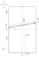
- FIG. 3 is a plan view of the electronic device assembly 1.
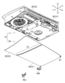
- FIG. 4 is an exploded perspective view of the electronic device assembly 1.
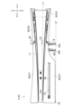
- FIG. 5A is a cross-sectional view of the electronic device assembly 1 taken along a cut plane including line VA-VA in FIG. 3.
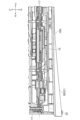
- FIG. 5B is a cross-sectional view of the electronic device assembly 1 taken along a cut plane including line VB-VB in FIG. 3.
- the Z1 and Z2 directions of the Z axis shown in FIG. 1 etc. are referred to as the upward and downward directions, respectively.
- the X1 and X2 directions of the X axis perpendicular to the Z axis are referred to as the rightward and leftward directions, respectively.
- the Y1 and Y2 directions of the Y axis perpendicular to the Z axis and X axis are referred to as the forward and backward directions, respectively.
- these directions are defined to explain the shapes of elements such as parts, members, and portions of electronic device assembly 1 and the relative positional relationships of each element, and do not limit the attitude of electronic device assembly 1 during use.
- the electronic device assembly 1 is a structure that combines an electronic device 10 and a stand for supporting the electronic device 10 (for example, a front stand 40a and a rear stand 40b described later).
- the electronic device 10 has a curved bottom surface 10D.
- the electronic device 10 has a device body 11 and a lower panel 20 (exterior panel) attached to the bottom surface 11D of the device body 11.
- the device body 11 houses a circuit board 15.
- the circuit board 15 is disposed inside the device body 11 in a position that intersects with the up-down direction (Z-axis direction).
- the circuit board 15 may be disposed in a position facing the lower panel 20.
- the circuit board 15 may be disposed in a position along the front-rear direction (Y-axis direction) and the left-right direction (X-axis direction).
- the curved bottom surface 10D of the electronic device 10 is formed by a bottom panel 20 (exterior panel).
- the bottom panel 20 has a left partial panel 21 (first partial panel) arranged on the left side (X2 side, right side in FIG. 4) of the device body 11, and a right partial panel 22 (second partial panel) arranged on the right side (X1 side, left side in FIG. 4) of the device body 11.
- the right partial panel 22 covers a part of the bottom surface 11D of the device body 11 (the part where the cooling fan 12 and the storage medium storage chamber 13 are provided), and the left partial panel 21 covers another part of the bottom surface 11D.
- the curved bottom surface 10D of the electronic device 10 is formed by the bottom surface of the right partial panel 22 and the bottom surface of the left partial panel 21.
- the lower panel 20 (left partial panel 21 and right partial panel 22) is detachable from the device body 11. Furthermore, as shown in FIG. 1, the electronic device 10 has a curved upper panel 30 that covers the top surface of the device body 11. Like the lower panel 20, the upper panel 30 also has a right partial panel 32 arranged on the right side (X1 side, left side in FIG. 1) of the device body 11, and a left partial panel 31 arranged on the left side (X2 side, right side in FIG. 1) of the device body 11. The upper panel 30 (right partial panel 32 and left partial panel 31) may also be detachable from the device body 11.
- a gap G1 is formed between the left partial panel 21 and the right partial panel 22 that constitute the lower panel 20.
- the left partial panel 21 and the right partial panel 22 are separate members that are independent of each other. Therefore, as shown in FIG. 1, the gap G1 is formed continuously from the front end (end on the Y1 side) to the rear end (end on the Y2 side) of the lower panel 20.
- the gap G1 extends diagonally from the front end of the lower panel 20 to the rear and leftward (the direction indicated by X2, the rightward in FIG. 1).
- the gap G1 extends from the front end to the rear end of the electronic device 10 on the lower surface 10D of the electronic device 10, and is inclined in the left-right direction.
- the lower panel 20 has the left partial panel 21 and the right partial panel 22, and thus covers almost the entire lower surface 11D of the device body 11 except for the gap G1.
- the gap G1 that is not covered by the lower panel 20 exposes the areas where the mounting sections 50a and 50b, described below, are formed.
- the lower panel 20 may be formed integrally including the left partial panel 21 and the right partial panel 22.
- the right partial panel 22 may be connected to the left partial panel 21.
- the ventilation hole of the cooling fan 12 is formed inside the recess 14 recessed upward from the lower surface 11D of the device body 11.
- the right region (recess 14) of the lower surface 11D is recessed relative to the left region, and the ventilation hole of the cooling fan 12 is formed in this right region.
- An air flow path is formed between the right region (recess 14) of the lower surface 11D and the lower panel 20.
- the gap G1 between the left partial panel 21 and the right partial panel 22 overlaps with at least a portion of the recess 14 as shown in FIG. 2. That is, in the bottom view of the electronic device 10, the gap G1 is located inside the right region (recess 14) of the lower surface 11D.
- the gap G1 exposes at least a portion of the recess 14 downward.
- the gap G1 exposes the right end (the end on the X2 side) of the recess 14.
- the gap G1 functions as a ventilation hole, and an air flow path from the outside of the electronic device 10 to the cooling fan 12 can be secured.
- a gap G2 is formed between the right partial panel 32 and the left partial panel 31 constituting the upper panel 30.
- the gap G2 is formed continuously from the front end (end on the Y1 side) to the rear end (end on the Y2 side) of the upper panel 30, similar to the gap G1 (see FIG. 1), and extends diagonally from the front end of the lower panel 20 to the rear (Y2 direction) and to the left (X2 direction).
- the gap G1 of the lower panel 20 is formed at the same position as the gap G2 of the upper panel 30 in a plan view. In the plan view shown in FIG. 3, the gap G1 overlaps with the gap G2.
- the entire area of the gaps G1 and G2 is provided on the right side (X1 side) of the center position cx (see the dashed line) in the left-right direction (direction along the X axis in FIG. 3) of the electronic device 10.
- the electronic device assembly 1 has a front stand 40a (first stand, hereinafter also simply referred to as stand 40a) and a rear stand 40b (second stand, hereinafter also simply referred to as stand 40b) for supporting the electronic device 10.
- the stands 40a and 40b are detachable from the electronic device 10.
- the curved underside 10D of the electronic device 10 has an area a (first position) where the front stand 40a is provided, and an area b (second position) where the rear stand 40b is provided.
- the gap G1 of the lower panel 20 and the regions a and b in which the stands 40a and 40b are provided are provided on the opposite side (lower side) of the front side (upper side) shown in FIG. 3.
- the regions a and b are indicated by dotted lines.
- the region a is provided in front of the center position cy (see the dashed line) in the front-rear direction (direction along the Y axis in FIG. 3) of the electronic device 10, and the region b is provided on the rear side of the center position cy.
- the stands 40a and 40b can be attached and detached to these regions a and b.
- the stands 40a and 40b can be attached to the front and rear sides of the center position cy of the electronic device 10. As shown in FIG. 5B, the stands 40a and 40b support the electronic device 10 at positions shifted in the front-rear direction (Y-axis direction in FIG. 5B). This makes it possible to stably install the electronic device 10 on an installation surface L2 (see the dashed line in FIG. 5B) such as a floor surface.
- area a where the front stand 40a is provided is defined in the gap G1 between the left partial panel 21 and the right partial panel 22 that constitute the lower panel 20.
- area b where the rear stand 40b is provided is also defined in the gap G1 between the left partial panel 21 and the right partial panel 22.
- areas a and b are defined inside the gap G1 in a plan view.
- the underside 10D of the electronic device 10 is a virtual surface that connects the underside of the right partial panel 22 and the underside of the left partial panel 21 in the portion where the gap G1 is formed.
- the underside 11D of the device body 11 has a front mounting portion 50a (hereinafter also simply referred to as mounting portion 50a) to which the front stand 40a can be attached, and a rear mounting portion 50b (hereinafter also simply referred to as mounting portion 50b) to which the rear stand 40b can be attached.
- the mounting portions 50a and 50b have holes formed in the underside 11D. More specifically, as shown in Figure 5B, the front mounting portion 50a has holes 51 and 52. Also, the rear mounting portion 50b has holes 53 and 54.
- the holes 51 to 54 are lined up in this order from one side (the front side, the left side in Figure 5B) to the other side (the rear side, the right side in Figure 5B) in the direction along the circuit board 15 (see Figure 5A).
- the holes 51 to 54 are recesses in which the surface of the underside 11D of the device body 11 is recessed upward. Therefore, the members and electronic components housed in the device body 11 are not exposed through the holes 51 to 54.
- the holes 51 and 52 (see FIG. 5B) of the front mounting portion 50a are provided in the area a (see FIG. 3) inside the gap G1 between the left partial panel 21 and the right partial panel 22 that constitute the lower panel 20 in a plan view.
- the holes 53 and 54 (see FIG. 5B) of the rear mounting portion 50b are provided in the area b (see FIG. 3) inside the gap G1 in a plan view. Therefore, the holes 51 to 54 are exposed from the gap G1.
- the stands 40a and 40b are arranged apart from each other along the gap G1 on the underside 11D of the device body 11. This makes it possible to reduce the air resistance caused by the stands 40a and 40b with respect to the gap G1 that functions as an air vent for the cooling fan 12 (see FIG. 4).
- the curved bottom surface 10D of the electronic device 10 has a support portion 23 for supporting the electronic device 10, separate from the stands 40a, 40b.
- the support portion 23 is formed on the left partial panel 21 of the left partial panel 21 and right partial panel 22 that make up the lower panel 20.
- the support portion 23 is provided on a protrusion formed on the left partial panel 21. More specifically, the support portion 23 is the lower end of a protrusion formed on a corner 21E of the left partial panel 21 (the portion where the outer edge on the X2 side and the outer edge on the Y2 side are connected).
- Plane L1 is a plane that includes circuit board 15 and runs along the surface of circuit board 15.
- Plane L1 is a plane that is approximately parallel to installation surface L2 (see the two-dot chain lines in FIGS. 2 and 5B), such as the floor surface on which electronic device assembly 1 is installed.
- the lower ends of the stands 40a, 40b and the support parts 23 come into contact with the installation surface L2 (see the two-dot chain line in FIG. 2), such as the floor surface.
- the installation surface L2 see the two-dot chain line in FIG. 2
- the convex parts on which the support parts 23 are provided protrude downward from the bottom surface 10D of the electronic device 10. This prevents parts of the bottom surface 10D of the electronic device 10 other than the convex parts from directly contacting the installation surface L2.
- the left partial panel 21 and the right partial panel 22 that constitute the lower panel 20 may be formed from resin. Furthermore, the support portion 23 of the left partial panel 21 (for example, the entire protrusion on which the support portion 23 is provided) may be formed from a material that is softer than the resin used to form the panel, such as rubber or elastomer. This can prevent the support portion 23 from slipping against the installation surface L2, such as the floor surface.
- the distance from plane L1 (the plane including the circuit board 15 shown in FIG. 5A) to the bottom end of the front stand 40a is substantially the same as the distance from plane L1 to the support portion 23.
- the distance from plane L1 to the bottom end of the rear stand 40b is substantially the same as the distance from plane L1 to the support portion 23.
- the support portion 23 is formed at a corner portion 21E of the left partial panel 21.
- the width of the left partial panel 21 in the left-right direction (X-axis direction) along a plane L1 (see Fig. 2) including the circuit board 15 (see Fig. 5A) is greater than the width of the right partial panel 22 in the same direction.
- the distance from the front stand 40a to the support portion 23 and the distance from the rear stand 40b to the support portion 23 in the left-right direction are greater than half the length of the electronic device assembly 1 in the left-right direction. This makes it possible to support the electronic device 10 more stably.
- the gap G1 between the left partial panel 21 and the right partial panel 22 constituting the lower panel 20 extends in a direction oblique to the front-rear direction (Y-axis direction). Therefore, as shown in FIG. 2, the position of the front stand 40a attached to the front side of the electronic device 10 and the position of the rear stand 40b attached to the rear side are shifted in the left-right direction (X-axis direction) along the gap G1.
- One of the stands 40a, 40b is located to the left of the other.
- the front stand 40a is located to the right (X1 direction) of the rear stand 40b.
- the rear stand 40b is located to the left (X2 direction) of the front stand 40a.
- the stands 40a, 40b support the electronic device 10 at positions shifted in the left-right direction. This makes it possible to support the electronic device 10 more stably.
- the front stand 40a and the rear stand 40b have the same shape. This reduces the manufacturing costs of the front stand 40a and the rear stand 40b compared to when the front stand 40a and the rear stand 40b have different shapes.
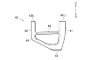
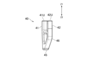
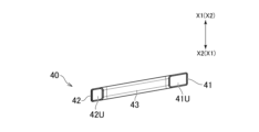
- Figures 6A to 6F show stand members 40, which are front stand 40a and rear stand 40b.
- Figure 6A is a front view of stand member 40.
- Figure 6B is a rear view of stand member 40.
- Figure 6C is a left side view of stand member 40.
- Figure 6D is a right side view of stand member 40.
- Figure 6E is a plan view of stand member 40.
- Figure 6F is a bottom view of stand member 40. Note that the "front”, “rear”, “right side” and “left side” here do not coincide with the front-rear and left-right directions indicated by the X-axis and Y-axis in Figures 1 to 5.
- the front stand 40a and the rear stand 40b face in opposite directions when attached to the electronic device 10.
- the front stand 40a faces the right side shown in Figure 6D
- the rear stand 40b faces the left side shown in Figure 6C.
- the front stand 40a and the rear stand 40b are arranged symmetrically side by side.
- each stand member 40 front stand 40a and rear stand 40b has two legs 41, 42 that are attached to the electronic device 10 in the vertical direction (Z-axis direction).
- Leg 41 first leg
- Leg 42 second leg
- Leg 41 first leg
- Leg 42 second leg
- the upper end 41U of the leg 41 (see FIG. 6A) is fitted into the hole 51 (first mounting portion) of the front mounting portion 50a, and the upper end 42U of the leg 42 (see FIG. 6A) is fitted into the hole 52 (second mounting portion) of the front mounting portion 50a.
- the upper end 41U of the leg 41 is fitted into the hole 54 (first mounting portion) of the rear mounting portion 50b, and the upper end 42U of the leg 42 is fitted into the hole 53 (second mounting portion) of the rear mounting portion 50b.
- the stands 40a and 40b are attached to the electronic device 10 (more specifically, to the underside 11D of the device body 11).
- the gap G1 between the left partial panel 21 and the right partial panel 22 constituting the lower panel 20 is provided on the opposite side (lower side) of the front side (upper side) shown in FIG. 3.
- the gap G1 extends in a diagonal direction (first direction) relative to the left-right direction (X-axis direction) and the front-rear direction (Y-axis direction).
- the legs 41, 42 formed on each stand member 40 are separated in the diagonal direction in which the gap G1 extends, as shown in FIG. 6E.
- the legs 41, 42 of the stand member 40 have a thickness in the left-right direction (X-axis direction) that corresponds to the width of the gap G1.
- the direction in which the legs 41, 42 are separated coincides with the direction in which the gap G1 extends, so that the legs 41, 42 of each stand member 40 can be inserted into the gap G1.
- the legs 41, 42 are connected by a beam 43 that extends along the gap G1. This provides reinforcement to the legs 41, 42.
- the beam 43 fits inside the gap G1 (see FIGS. 1 and 5B).
- the legs 41, 42 of the stand member 40 have a common bottom end 45.
- the bottom end 45 is the portion that comes into contact with the installation surface L2 (see FIG. 2, etc.) such as the floor surface, and is also referred to as the contact portion 45 below.
- the entire stand member 40 may be formed from resin.
- the contact portion 45 may be formed from a material that is softer than resin, such as rubber or elastomer. This ensures the strength of the stand member 40 and prevents the stands 40a, 40b from slipping on the installation surface L2.
- leg 41 of stand member 40 is slightly curved and connects to contact portion 45 at the lower end.
- a bent portion 46 bent toward contact portion 45 is formed between upper end 42U of leg 42 and contact portion 45.
- leg 41 of stand member 40 is thicker in the diagonal direction along gap G1 (left-right direction in FIG. 6A) than leg 42. In this way, by providing two legs 41, 42 that connect to contact portion 45, and further increasing the thickness of leg 41 that extends from contact portion 45 without bending, the strength of stand member 40 can be ensured.
- the hole 51 (first mounting portion) of the front mounting portion 50a and the hole 54 (first mounting portion) of the rear mounting portion 50b into which the leg 41 of the stand member 40 is fitted have a width corresponding to the leg 41.
- the width d1 of the hole 51 and the width d4 of the hole 54 are the same and approximately match the width of the leg 41.
- the hole 52 (second mounting portion) of the front mounting portion 50a and the hole 53 (second mounting portion) of the rear mounting portion 50b into which the leg 42 of the stand member 40 is fitted also have a width corresponding to the leg 42.
- the width d2 of the hole 52 and the width d3 of the hole 53 are the same and approximately match the width of the leg 42.
- the distance d5 between the holes 51 and 52 of the front mounting portion 50a is also the same as the distance d6 between the holes 53 and 54 of the rear mounting portion 50b.
- the distances d5 and d6 are approximately the same as the distance between the leg portion 41 and the leg portion 42. For this reason, it is possible to attach stand members 40 of the same shape to the front mounting portion 50a and the rear mounting portion 50b as the front stand 40a and the rear stand 40b. 3. Modifications It should be noted that the present invention is not limited to the above-described embodiments.
- FIG. 7 is a front view of electronic device assembly 1, which is another example of an embodiment.
- a left partial panel 27 is attached, which has a different shape from left partial panel 21 shown in FIG. 2.
- left partial panel 27 and right partial panel 22 form lower panel 20 and curved lower surface 10D of electronic device 10.
- the left partial panel 27 shown in FIG. 7 bulges downward (in the Z2 direction) more than the left partial panel 21 shown in FIG. 2.
- an optical disk drive 18 is disposed between the bottom surface 11D (see FIG. 4) of the device body 11 and the left partial panel 27.
- An opening 28 is formed in the left partial panel 27. The opening 28 exposes the optical disk drive 18 to the front.
- the electronic device assembly 1 shown in FIG. 7, like that shown in FIG. 2, has a front stand 60a (first stand, hereinafter also referred to as stand 60a) and a rear stand 60b (second stand, hereinafter also referred to as stand 60b) for supporting the electronic device 10.
- the curved underside 10D of the electronic device 10 has an area (first position) where the front stand 60a is provided and an area (second position) where the rear stand 60b is provided in the gap G1 between the left partial panel 27 and the right partial panel 22.
- Mounting portions 50a, 50b (see FIG. 4) to which the stands 60a, 60b are attached are formed in these areas.
- the left partial panel 27 has a support portion 29 for supporting the electronic device 10.
- the support portion 29 is the lower end of a protrusion formed on the left partial panel 21.
- the distance in the vertical direction (Z-axis direction) from the plane L1 (see FIG. 5A and the two-dot chain line in FIG. 7) including the circuit board 15 (see FIG. 5A) to the underside 10D is maximum at the support portion 29.
- the support portion 29 is made of a material that is softer than resin, such as rubber or elastomer, and thus the support portion 29 can be prevented from slipping against the installation surface L2, such as the floor surface.
- the lower ends of the stands 60a, 60b and the support parts 29 come into contact with the installation surface L2 (see the two-dot chain line in FIG. 7), such as the floor surface, allowing the electronic device 10 to be stably installed.
- the support parts 29 are provided at the lower ends of the convex parts, it is possible to prevent parts of the underside 10D of the electronic device 10 other than the convex parts from directly contacting the installation surface L2.
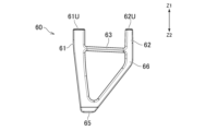
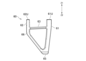
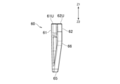
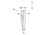
- FIGS. 8A to 8F show a stand member 60 which is the front stand 60a and the rear stand 60b.
- FIG. 8A is a front view of the stand member 60.
- FIG. 8B is a rear view of the stand member 60.
- FIG. 8C is a left side view of the stand member 60.
- FIG. 8D is a right side view of the stand member 60.
- FIG. 8E is a plan view of the stand member 60.
- FIG. 8F is a bottom view of the stand member 60. Note that the "front”, “rear”, “right side” and “left side” here do not coincide with the front-rear and left-right directions indicated by the X-axis and Y-axis in FIG. 7.
- the stand member 60 which is the front stand 60a and the rear stand 60b, has two legs 61 and 62, similar to the stand member 40 shown in FIG. 6A and the like.
- the leg 61 first leg
- the leg 62 (second leg) has an upper end 62U that fits into the hole 52 or the hole 53 (second mounting portion, see FIG. 5B) of the electronic device 10, and extends downward from the upper end 42U.
- the legs 61 and 62 have a contact portion 65 as a common lower end.
- the contact portion 65 is made of rubber, elastomer, or the like, so that the stand member 60 can be prevented from slipping on the installation surface L2.
- the distance from plane L1 including circuit board 15 to support portion 29 is greater than the distance from plane L1 to support portion 23 shown in FIG. 2.
- Electronic device 10 shown in FIG. 7 is taller in the vertical direction (Z-axis direction) than electronic device 10 shown in FIG. 2. Therefore, stand member 60 (see FIG. 8A, etc.) for supporting electronic device 10 in FIG. 7 is also taller in the vertical direction than stand member 40 (see FIG. 6A, etc.). In this way, electronic device 10 can be stably installed on installation surface L2, such as the floor surface, by support portion 29 and stand member 60 (stand 60a, stand 60b).
- the number of stands attached to the electronic device 10 may be one, or three or more.
- the front stand 40a and rear stand 40b shown in FIG. 5B may be configured as a single member.
- a beam portion may be formed between the leg portion 42 of the front stand 40a and the leg portion 42 of the rear stand 40b to connect the two legs 42.
- the beam portion between the two legs 42 may extend in a rod or plate shape along the gap G1. In this way, the electronic device 10 can be stably installed on the installation surface L2 using the stand and support portion 23.
- the support portion 23 for supporting the electronic device 10 is the lower end of a convex portion formed on the lower surface 10D.
- the shape of the support portion 23 viewed from below (Z2 direction) is rectangular, but the shape of the support portion 23 is not limited to this.
- the shape of the support portion 23 may be, for example, a polygon such as a triangle or a pentagon, or may be a circle or an oval.
- the shape of the support portion 23 may be a cross shape, or a shape that imitates other letters or symbols.
- the number of protrusions and support parts 23 provided on the underside 10D of the electronic device 10 is not limited to one, and may be multiple.
- the size and shape of the multiple support parts 23 when the electronic device 10 is viewed from below (Z2 direction) may be the same or different from each other.
- protrusions in the shape of a triangle, circle, cross, or square may be lined up on the underside 10D of the electronic device 10, and the support parts 23 may be formed by these protrusions.
- the electronic device assembly described in the present disclosure includes an electronic device and a first stand for supporting the electronic device, the first stand being detachable from the electronic device.
- the electronic device has a curved lower surface and a circuit board arranged in a manner intersecting the vertical direction.
- the curved lower surface has a first position where the first stand is provided and a support portion at which the distance from a plane including the circuit board is maximum on the curved lower surface. This allows the electronic device to be stably installed.
- the electronic device has a curved lower surface and a circuit board arranged in a cross-position relative to the vertical direction.
- the curved lower surface has a first position where a first stand is provided and a support portion at which the distance from a plane including the circuit board is maximum on the curved lower surface. This allows the electronic device to be stably installed using the stand.
- the stand according to the present disclosure is a stand that is detachable from an electronic device, and has a first leg having an upper end for fitting into a first mounting portion of the electronic device and extending downward from the upper end, and a second leg having an upper end for fitting into a second mounting portion of the electronic device and extending downward from the upper end.
- the first leg and the second leg have a common lower end. This allows the electronic device to be stably installed.
- the distance from a plane including the circuit board to a lower end of the first stand may be substantially the same as the distance from the plane including the circuit board to the support portion.
- the electronic device may further include a device main body housing the circuit board, and an exterior panel attached to a lower surface of the device main body.
- the curved lower surface may be formed on the exterior panel.
- the exterior panel may include a first partial panel covering a portion of the lower surface of the device main body, and a second partial panel covering another portion of the lower surface of the device main body.
- the first position where the first stand is provided may be defined in a gap between the first partial panel and the second partial panel.
- a bottom surface of the device body may have an attachment portion to which the first stand can be attached.
- a second stand for supporting the electronic device may be provided.
- the curved lower surface may have a second position where the second stand is provided.
- the electronic device may have a device main body housing the circuit board and an exterior panel attached to a lower surface of the device main body.
- the curved lower surface may be formed on the exterior panel.
- the exterior panel may have a first partial panel covering a portion of the lower surface of the device main body and a second partial panel covering another portion of the lower surface of the device main body. The first position where the first stand is provided and the second position where the second stand is provided may be defined in a gap between the first partial panel and the second partial panel.
- the first stand and the second stand may have the same shape.
- the support portion may be formed on the first partial panel, and a width of the first partial panel in a direction along a plane including the circuit board may be larger than a width of the second partial panel in the same direction.
- the support portion may be provided on a protrusion formed on the first partial panel.
- the gap may extend in a first direction along a plane including the circuit board, and the first stand may have at least two legs spaced apart in the first direction and attached to the electronic device.
Landscapes
- Engineering & Computer Science (AREA)
- Theoretical Computer Science (AREA)
- Physics & Mathematics (AREA)
- Computer Hardware Design (AREA)
- General Engineering & Computer Science (AREA)
- Human Computer Interaction (AREA)
- General Physics & Mathematics (AREA)
- Power Engineering (AREA)
- Electromagnetism (AREA)
- Microelectronics & Electronic Packaging (AREA)
- Casings For Electric Apparatus (AREA)
Priority Applications (3)
| Application Number | Priority Date | Filing Date | Title |
|---|---|---|---|
| CN202480012631.7A CN120642585A (zh) | 2023-02-21 | 2024-02-14 | 电子设备组件、电子设备和支架 |
| EP24760221.2A EP4672877A1 (en) | 2023-02-21 | 2024-02-14 | ELECTRONIC DEVICE ASSEMBLY, ELECTRONIC DEVICE AND SUPPORT |
| JP2025502303A JPWO2024176920A1 (https=) | 2023-02-21 | 2024-02-14 |
Applications Claiming Priority (2)
| Application Number | Priority Date | Filing Date | Title |
|---|---|---|---|
| JP2023-025545 | 2023-02-21 | ||
| JP2023025545 | 2023-02-21 |
Publications (1)
| Publication Number | Publication Date |
|---|---|
| WO2024176920A1 true WO2024176920A1 (ja) | 2024-08-29 |
Family
ID=92501100
Family Applications (1)
| Application Number | Title | Priority Date | Filing Date |
|---|---|---|---|
| PCT/JP2024/005081 Ceased WO2024176920A1 (ja) | 2023-02-21 | 2024-02-14 | 電子機器組立体、電子機器、及びスタンド |
Country Status (4)
| Country | Link |
|---|---|
| EP (1) | EP4672877A1 (https=) |
| JP (1) | JPWO2024176920A1 (https=) |
| CN (1) | CN120642585A (https=) |
| WO (1) | WO2024176920A1 (https=) |
Citations (7)
| Publication number | Priority date | Publication date | Assignee | Title |
|---|---|---|---|---|
| JPS4740252Y1 (https=) * | 1968-06-06 | 1972-12-06 | ||
| JP2008147475A (ja) * | 2006-12-12 | 2008-06-26 | Nec Infrontia Corp | 卓上設置と壁掛け設置の兼用機器のベース部材 |
| WO2013154041A1 (ja) * | 2012-04-13 | 2013-10-17 | 株式会社ソニー・コンピュータエンタテインメント | 電子機器 |
| JP2018179850A (ja) * | 2017-04-18 | 2018-11-15 | 株式会社東海ヒット | 筐体支持構造、電子機器 |
| JP2020077672A (ja) * | 2018-11-05 | 2020-05-21 | カシオ計算機株式会社 | 脚部、脚部の取付構造および携帯端末 |
| WO2021193881A1 (ja) | 2020-03-27 | 2021-09-30 | 株式会社ソニー・インタラクティブエンタテインメント | 電子機器及びその外装パネル |
| WO2021230246A1 (ja) * | 2020-05-15 | 2021-11-18 | 株式会社ソニー・インタラクティブエンタテインメント | 電子機器のスタンド、及び電子機器組立体 |
-
2024
- 2024-02-14 WO PCT/JP2024/005081 patent/WO2024176920A1/ja not_active Ceased
- 2024-02-14 CN CN202480012631.7A patent/CN120642585A/zh active Pending
- 2024-02-14 JP JP2025502303A patent/JPWO2024176920A1/ja active Pending
- 2024-02-14 EP EP24760221.2A patent/EP4672877A1/en active Pending
Patent Citations (7)
| Publication number | Priority date | Publication date | Assignee | Title |
|---|---|---|---|---|
| JPS4740252Y1 (https=) * | 1968-06-06 | 1972-12-06 | ||
| JP2008147475A (ja) * | 2006-12-12 | 2008-06-26 | Nec Infrontia Corp | 卓上設置と壁掛け設置の兼用機器のベース部材 |
| WO2013154041A1 (ja) * | 2012-04-13 | 2013-10-17 | 株式会社ソニー・コンピュータエンタテインメント | 電子機器 |
| JP2018179850A (ja) * | 2017-04-18 | 2018-11-15 | 株式会社東海ヒット | 筐体支持構造、電子機器 |
| JP2020077672A (ja) * | 2018-11-05 | 2020-05-21 | カシオ計算機株式会社 | 脚部、脚部の取付構造および携帯端末 |
| WO2021193881A1 (ja) | 2020-03-27 | 2021-09-30 | 株式会社ソニー・インタラクティブエンタテインメント | 電子機器及びその外装パネル |
| WO2021230246A1 (ja) * | 2020-05-15 | 2021-11-18 | 株式会社ソニー・インタラクティブエンタテインメント | 電子機器のスタンド、及び電子機器組立体 |
Non-Patent Citations (1)
| Title |
|---|
| See also references of EP4672877A1 |
Also Published As
| Publication number | Publication date |
|---|---|
| JPWO2024176920A1 (https=) | 2024-08-29 |
| CN120642585A (zh) | 2025-09-12 |
| EP4672877A1 (en) | 2025-12-31 |
Similar Documents
| Publication | Publication Date | Title |
|---|---|---|
| JP4508214B2 (ja) | 表示装置 | |
| JP4357579B1 (ja) | 電子機器 | |
| KR20170014504A (ko) | 기판 유닛과 기판 어셈블리 및 그것을 이용한 카메라 모듈 | |
| WO2024176920A1 (ja) | 電子機器組立体、電子機器、及びスタンド | |
| US7429181B2 (en) | Electrical connector assembly having improved pickup cap | |
| JP5895091B1 (ja) | 光モジュール | |
| JP7732086B2 (ja) | 電子機器 | |
| US7075787B2 (en) | Heat dissipating structure for computer casing | |
| JP7732085B2 (ja) | 電子機器 | |
| JP7547100B2 (ja) | ゲームコントローラ | |
| TW202230900A (zh) | 電子元件 | |
| JP3958763B2 (ja) | プラズマディスプレイ装置用シャーシベースユニット及びプラズマディスプレイ装置 | |
| JP4600224B2 (ja) | 電子機器及びそれに用いるコネクタ接続構造 | |
| WO2024214633A1 (ja) | スタンド装置 | |
| JP4033058B2 (ja) | 加速度センサ | |
| JP7776621B2 (ja) | センサ装置 | |
| JP7372582B1 (ja) | 電子機器の冷却構造 | |
| JP3582236B2 (ja) | 光ディスク装置 | |
| JP7810006B2 (ja) | 放熱器固定構造 | |
| JP7842913B1 (ja) | 電子機器 | |
| JP7803185B2 (ja) | 電子機器の筐体構造 | |
| WO2025216089A1 (ja) | 電子機器 | |
| JPH0733295Y2 (ja) | 車輌用灯具 | |
| KR20250151456A (ko) | 전자 디바이스 및 외장 패널 | |
| JP2000196250A (ja) | 電子回路基板保護装置 |
Legal Events
| Date | Code | Title | Description |
|---|---|---|---|
| 121 | Ep: the epo has been informed by wipo that ep was designated in this application |
Ref document number: 24760221 Country of ref document: EP Kind code of ref document: A1 |
|
| WWE | Wipo information: entry into national phase |
Ref document number: 202480012631.7 Country of ref document: CN |
|
| ENP | Entry into the national phase |
Ref document number: 2025502303 Country of ref document: JP Kind code of ref document: A |
|
| WWE | Wipo information: entry into national phase |
Ref document number: 2025502303 Country of ref document: JP |
|
| WWP | Wipo information: published in national office |
Ref document number: 202480012631.7 Country of ref document: CN |
|
| WWE | Wipo information: entry into national phase |
Ref document number: 2024760221 Country of ref document: EP |
|
| NENP | Non-entry into the national phase |
Ref country code: DE |
|
| ENP | Entry into the national phase |
Ref document number: 2024760221 Country of ref document: EP Effective date: 20250922 |
|
| ENP | Entry into the national phase |
Ref document number: 2024760221 Country of ref document: EP Effective date: 20250922 |
|
| WWP | Wipo information: published in national office |
Ref document number: 2024760221 Country of ref document: EP |