WO2024176803A1 - 透明導電膜、透明導電膜付基板、および光電変換素子 - Google Patents
透明導電膜、透明導電膜付基板、および光電変換素子 Download PDFInfo
- Publication number
- WO2024176803A1 WO2024176803A1 PCT/JP2024/003815 JP2024003815W WO2024176803A1 WO 2024176803 A1 WO2024176803 A1 WO 2024176803A1 JP 2024003815 W JP2024003815 W JP 2024003815W WO 2024176803 A1 WO2024176803 A1 WO 2024176803A1
- Authority
- WO
- WIPO (PCT)
- Prior art keywords
- conductive film
- transparent conductive
- layer
- film
- substrate
- Prior art date
- Legal status (The legal status is an assumption and is not a legal conclusion. Google has not performed a legal analysis and makes no representation as to the accuracy of the status listed.)
- Ceased
Links
Images




Classifications
-
- H—ELECTRICITY
- H01—ELECTRIC ELEMENTS
- H01B—CABLES; CONDUCTORS; INSULATORS; SELECTION OF MATERIALS FOR THEIR CONDUCTIVE, INSULATING OR DIELECTRIC PROPERTIES
- H01B5/00—Non-insulated conductors or conductive bodies characterised by their form
- H01B5/14—Non-insulated conductors or conductive bodies characterised by their form comprising conductive layers or films on insulating-supports
-
- H—ELECTRICITY
- H10—SEMICONDUCTOR DEVICES; ELECTRIC SOLID-STATE DEVICES NOT OTHERWISE PROVIDED FOR
- H10F—INORGANIC SEMICONDUCTOR DEVICES SENSITIVE TO INFRARED RADIATION, LIGHT, ELECTROMAGNETIC RADIATION OF SHORTER WAVELENGTH OR CORPUSCULAR RADIATION
- H10F10/00—Individual photovoltaic cells, e.g. solar cells
- H10F10/10—Individual photovoltaic cells, e.g. solar cells having potential barriers
- H10F10/16—Photovoltaic cells having only PN heterojunction potential barriers
- H10F10/164—Photovoltaic cells having only PN heterojunction potential barriers comprising heterojunctions with Group IV materials, e.g. ITO/Si or GaAs/SiGe photovoltaic cells
- H10F10/165—Photovoltaic cells having only PN heterojunction potential barriers comprising heterojunctions with Group IV materials, e.g. ITO/Si or GaAs/SiGe photovoltaic cells the heterojunctions being Group IV-IV heterojunctions, e.g. Si/Ge, SiGe/Si or Si/SiC photovoltaic cells
- H10F10/166—Photovoltaic cells having only PN heterojunction potential barriers comprising heterojunctions with Group IV materials, e.g. ITO/Si or GaAs/SiGe photovoltaic cells the heterojunctions being Group IV-IV heterojunctions, e.g. Si/Ge, SiGe/Si or Si/SiC photovoltaic cells the Group IV-IV heterojunctions being heterojunctions of crystalline and amorphous materials, e.g. silicon heterojunction [SHJ] photovoltaic cells
-
- H—ELECTRICITY
- H10—SEMICONDUCTOR DEVICES; ELECTRIC SOLID-STATE DEVICES NOT OTHERWISE PROVIDED FOR
- H10F—INORGANIC SEMICONDUCTOR DEVICES SENSITIVE TO INFRARED RADIATION, LIGHT, ELECTROMAGNETIC RADIATION OF SHORTER WAVELENGTH OR CORPUSCULAR RADIATION
- H10F77/00—Constructional details of devices covered by this subclass
- H10F77/20—Electrodes
Definitions
- the present invention relates to a transparent conductive film, a substrate with a transparent conductive film, and a photoelectric conversion element.
- In2O3 -based materials such as ITO (tin-doped indium oxide) are widely known as transparent conductive films for light-receiving transparent electrodes of optoelectronic devices such as displays and solar cells (see, for example, Patent Document 1) .
- ITO in-doped indium oxide
- In2O3 - based materials have the advantages of being capable of being formed into films by low-temperature processes and of having both high transparency and electrical conductivity.
- indium is a rare metal and very expensive, it is being considered to replace In2O3 - based materials with other materials.
- a transparent conductive film that is relatively inexpensive and can be formed at low temperatures a film made of ZnO (zinc oxide) is known (for example, Patent Document 2).
- a transparent conductive film mainly made of zinc oxide has low moisture resistance and chemical resistance. Therefore, it has been difficult to replace a transparent conductive film mainly made of zinc oxide with a transparent conductive film made of ITO or the like.
- films containing SnO 2 such as FTO (fluorine-doped tin oxide) and ATO (antimony-doped tin oxide), are also known as transparent conductive films that are highly transparent and have excellent stability and chemical resistance.
- FTO and ATO are polycrystalline, and the conductivity is increased by forming the film at a high temperature and improving the crystallinity. Therefore, the FTO film and ATO film need to be formed at about 500°C by thermal CVD, or at 400°C to 500°C by sputtering.
- film formation at a high temperature exceeding 400°C is likely to cause thermal damage to the substrate on which the film is laminated and each layer of the optoelectronic device. Therefore, it has been difficult to use FTO and ATO as the transparent conductive film of the optoelectronic device. Therefore, in the current situation, it has been necessary to use a transparent conductive film of In 2 O 3 system mainly composed of rare indium.
- the present invention has been made in consideration of the above problems.
- the present invention aims to provide a transparent conductive film that can be formed at low temperatures, has high transparency and high conductivity, and further contains a small amount of indium or does not contain indium, as well as a transparent conductive film-coated substrate and a photoelectric conversion element that contain the same.
- One embodiment of the present invention provides a transparent conductive film comprising a metal oxide mainly composed of amorphous tin oxide, in which, among metal elements constituting the metal oxide, the amount of Sn is 85 atomic % or more and the amount of In is 4 atomic % or less, and the film has a resistivity of 2 ⁇ 10 ⁇ 3 ⁇ cm or less.
- One embodiment of the present invention also provides a substrate with a transparent conductive film, comprising a substrate and the above-described transparent conductive film disposed on the substrate.
- one embodiment of the present invention provides a photoelectric conversion element having a photoelectric conversion layer, a first electrode including at least one conductive film arranged adjacent to the photoelectric conversion layer, and a second electrode including at least one conductive film arranged adjacent to the photoelectric conversion layer, in which at least one of the first electrode and the second electrode includes the transparent conductive film.
- the present invention provides a transparent conductive film that can be formed at low temperatures, has high transparency and high conductivity, and contains little or no indium.
- the transparent conductive film can also be applied to various photoelectric conversion elements such as solar cells.
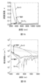
- FIG. 1A is a graph for explaining the correlation between the valence of Sn in a transparent conductive film and the extinction coefficient k
- FIG. 1B is a graph for explaining the correlation between the valence of Sn in a transparent conductive film and the absorption coefficient ⁇ .
- FIG. 2 is a graph showing the relationship between the depth from the surface of the transparent conductive film and the hydrogen atom concentration in the transparent conductive film.
- FIG. 3 is a schematic diagram of a reactive plasma deposition apparatus capable of forming a transparent conductive film according to one embodiment of the present invention.
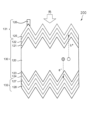
- FIG. 4 is a schematic diagram showing the structure of a Si heterojunction solar cell.
- FIG. 5 is a schematic diagram showing the structure of a perovskite solar cell.
- FIG. 1A is a graph for explaining the correlation between the valence of Sn in a transparent conductive film and the extinction coefficient k
- FIG. 1B is a graph for explaining the correlation between the valence of Sn in a transparent
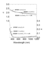
- FIG. 6 is a graph showing the extinction coefficient k and refractive index n for each wavelength of the amorphous SnO 2 films produced in Examples 1-1 and 1-2 and the a-In 2 O 3 :H film produced in Reference Example 1.
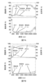
- FIG. 7A is a graph showing the transmission spectrum and the reflection spectrum of the PET substrate only, the PET substrate and the transparent conductive film (Example 1-3), and the PET substrate with SiO2 and the transparent conductive film (Example 1-4).
- FIG. 7B is a graph showing the transmission spectrum and the reflection spectrum of the glass substrate only, and the glass substrate and the transparent conductive film (Example 1-3, Example 1-4).
- FIG. 7A is a graph showing the transmission spectrum and the reflection spectrum of the PET substrate only, the PET substrate and the transparent conductive film (Example 1-3), and the PET substrate with SiO2 and the transparent conductive film (Example 1-4).
- FIG. 7B is a graph showing the transmission spectrum and the reflection spectrum of the glass substrate only, and the
- FIG. 8 shows the external quantum efficiency spectra of the front junction Si heterojunction solar cells fabricated in Examples 2-1 and 2-2, and Reference Example 2.
- FIG. 9 is a graph showing the current-voltage characteristics of the rear junction Si heterojunction solar cells fabricated in Examples 3-1 and 3-2, and Reference Example 3.
- FIG. 10 is a graph showing the current-voltage characteristics of the rear junction Si heterojunction solar cells fabricated in Example 3-2a and Reference Example 3.
- FIG. 11 is a graph showing the series resistance values of the Si heterojunction solar cells fabricated in each example.
- a numerical range indicated with “ ⁇ ” means a numerical range including the numbers written before and after " ⁇ ".
- the transparent conductive film of the present invention contains a metal oxide mainly composed of amorphous tin oxide, and among the metal elements constituting the metal oxide, the amount of Sn is 85 atomic % or more, the amount of In is 4 atomic % or less, and the resistivity is 2 ⁇ 10 ⁇ 3 ⁇ cm or less.
- the tin oxide in the transparent conductive film is "amorphous" means that when the X-ray diffraction intensity (XRD intensity) is measured, a broad peak derived from the amorphous structure is dominant and a peak derived from the crystal is not significantly confirmed.
- the transparent conductive film may partially contain components other than the above metal oxide, for example, may be doped with fluorine, within a range that does not impair the object and effect of the present invention, but it is preferable that 85 mass % or more of the transparent conductive film is the above metal oxide, and it is more preferable that the transparent conductive film is made of the above metal oxide.
- polycrystalline FTO SnO 2 :F
- ATO SnO 2 :Sb
- a film mainly containing amorphous tin oxide can not only be formed at low temperatures, but also has excellent transparency and conductivity. The reason for this is believed to be as follows.
- the conduction band of tin oxide (especially SnO 2 ) is mainly composed of Sn5s orbitals.
- the Sn5s orbitals have a large spatial spread of electrons, and the spherical s orbitals overlap each other. Therefore, even if the bond angle fluctuates due to the amorphous structure, the overlap between the orbitals does not decrease as much as in the case of crystalline materials, and it is considered that high mobility of electrons is realized.
- the effective mass of electrons in a film made of amorphous SnO 2 is 0.35 m 0 , which is not significantly different from the effective mass of electrons in a film made of crystalline SnO 2. Therefore, it is considered that the carrier conduction path is not easily affected by the amorphous structure, and the amorphous tin oxide (especially SnO 2 ) realizes high transparency and high conductivity similar to those of crystalline SnO 2 .
- the transparent conductive film of the present invention also has the advantage of having good moisture resistance.
- the metal oxide may contain metal elements other than Sn within a range that does not impair the purpose and effect of the present invention, but the total amount is preferably 15 atomic % or less, more preferably 10 atomic % or less, and even more preferably 5 atomic % or less, of all metal elements constituting the metal oxide.
- metal elements other than Sn contained in the metal oxide include In, Zn, Cd, Nb, Ta, B, Ga, Ba, Mo, Pb, Rb, Re, Sb, W, Ce, Cs, Dy, Er, Ge, Hf, Ho, La, Lu, Nd, Pr, Sc, Si, Sm, Tb, V, Y, Al, Ti, Zr, etc., and among these, Zn, Cd, B, Ga, Si, Ge, Pb, Sb, V, Nb, Ta, Mo, W, and Ce are preferred.
- the metal oxide may contain only one of these, or may contain two or more. When the metal oxide further contains a metal element other than Sn, the processability of the material for forming the transparent conductive film is improved, and depending on the type of metal element, the density, transparency, and conductivity of the transparent conductive film are further improved.
- the amount of In relative to the total amount of metal elements constituting the metal oxide is 4 atomic % or less, preferably 3 atomic % or less, preferably 0.09 atomic % or less, and more preferably substantially none.
- the lower the amount of In the lower the cost of the transparent conductive film.
- the metal oxide transparent conductive film
- the metal oxide does not contain In, it is not subject to regulation, and there is an advantage in that workability is improved.
- the amount of each metal element constituting the metal oxide can be identified by, for example, confirming the composition of the transparent conductive film using ICP analysis.
- Sn is mainly contained in a tetravalent (Sn 4+ ) state.
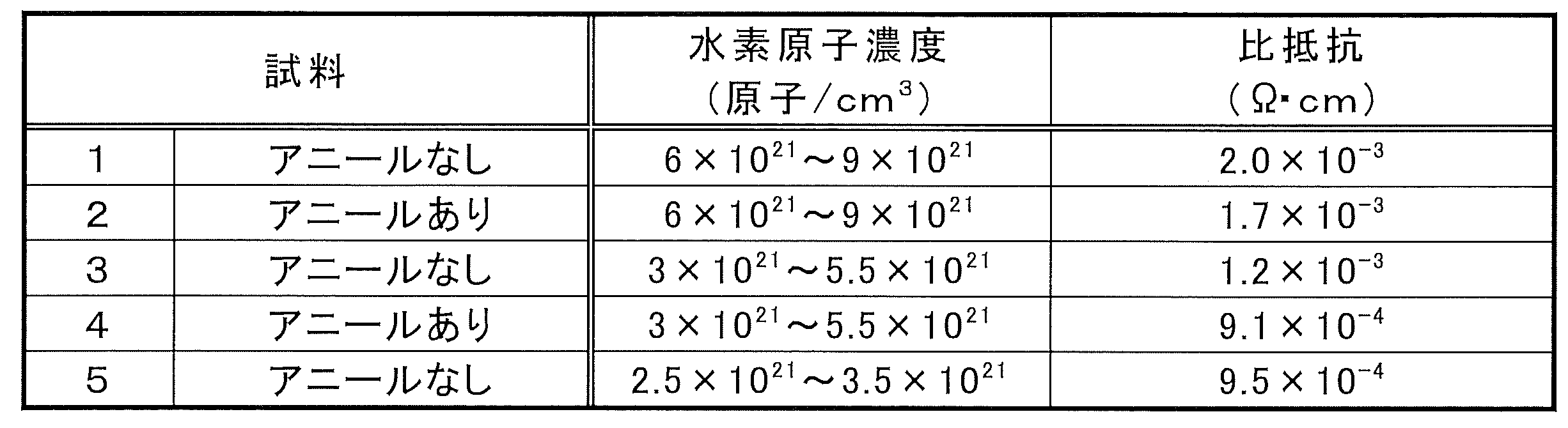
- Sn can have a mixed valence of Sn 4+ and Sn 2+ , but as the amount of Sn 2+ in the transparent conductive film increases, the number of acceptor-type defects increases. As a result, both the carrier concentration and the mobility decrease, and the resistivity tends to increase, as shown in Table 1 below.
- FIG. 1A shows the extinction coefficient k at a wavelength of 200 nm or more and 1200 nm or less when the ratio of the amount of Sn 4+ to the amount of Sn 2+ is changed.
- FIG. 1B shows the absorption coefficient ⁇ at wavelengths of 400 nm or more and 600 nm or less when the ratio of the amount of Sn 4+ to the amount of Sn 2+ is changed.
- the maximum absorption coefficient ⁇ in the wavelength range of 420 nm to 500 nm is 1 ⁇ 10 4 cm ⁇ 1 or less, it can be said that the amount of tetravalent Sn in the transparent conductive film is sufficiently large, and high transparency and high conductivity are more easily achieved.
- the absorption coefficient ⁇ can be determined from the absorption spectrum obtained by measuring the transmittance and reflectance of light having a wavelength of 200 nm or more and 1200 nm or less using a spectrophotometer.
- the method for adjusting the extinction coefficient k or absorption coefficient ⁇ in the transparent conductive film can be adjusted by depositing the transparent conductive film in an atmosphere containing a sufficient amount of oxygen, reducing the partial pressure of water vapor remaining in the deposition chamber, or by heating the film to a temperature of about 200°C or less.
- the resistivity of the transparent conductive film may be 2 ⁇ 10 ⁇ 3 ⁇ cm or less, preferably 1.5 ⁇ 10 ⁇ 3 ⁇ cm or less, and more preferably 1 ⁇ 10 ⁇ 3 ⁇ cm or less. If the resistivity of the transparent conductive film is 2 ⁇ 10 ⁇ 3 ⁇ cm or less, the transparent conductive film can be used for various applications, such as a transparent electrode of a photoelectric conversion element.
- the resistivity can be determined by a Loresta (low resistivity meter).
- the film density of the transparent conductive film is preferable for the film density of the transparent conductive film to be as high as possible.
- the following four samples were produced using a method similar to that shown in Example 1-1 described below.
- the composition, film density, and resistivity at this time are shown in Table 1 below.
- the average composition was analyzed using the Rutherford backscattering spectrometry (RBS) method, and the resistivity was measured using a Loresta (low resistivity meter).
- the film density was calculated from the areal density determined by the RBS method and the film thickness determined by spectroscopic ellipsometry.
- the resistivity decreases as the film density of the transparent conductive film increases.
- the film density analyzed by the Rutherford backscattering spectrometry (RBS) method is 5.6 g/cm 3 or more, more preferably 6.3 g/cm 3 or more, and even more preferably 6.4 g/cm 3 or more.
- RBS Rutherford backscattering spectrometry
- the concentration of hydrogen atoms in the region 10 nm or more inside from each of both surfaces of the transparent conductive film is preferably 8 ⁇ 10 21 atoms/cm 3 or less, more preferably 7 ⁇ 10 21 atoms/cm 3 or less, and even more preferably 6 ⁇ 10 21 atoms/cm 3 or less.
- the thickness of the transparent conductive film is appropriately selected depending on the application.
- the thickness is preferably 1 nm or more and 5000 nm or less, and more preferably 10 nm or more and 1000 nm or less.
- the thickness of the transparent conductive film is within this range, it becomes easier to obtain the high transparency and high conductivity required for a transparent electrode.
- the method for producing the transparent conductive film is not particularly limited as long as the above-mentioned composition and resistivity are satisfied, and the film can be formed by, for example, a film formation method using reactive plasma deposition or a sputtering method.
- a film formation method using reactive plasma deposition is described below, but the method for producing the transparent conductive film is not limited to this method.
- a method for forming a transparent conductive film by magnetron sputtering is also shown.
- Film formation using the reactive plasma deposition method can be performed, for example, by a reactive plasma deposition apparatus 100 shown in the schematic diagram of FIG. 3.
- a reactive plasma deposition apparatus 100 shown in the schematic diagram of FIG. 3.
- the configuration of the reactive plasma deposition apparatus 100 is not limited to this configuration.
- the reactive plasma deposition apparatus 100 has a hearth section 10 for holding the material at a predetermined temperature, a plasma gun 20 for generating a plasma beam 21 and a plasma 22, a plasma beam controller 30 for directing the plasma beam 21 generated from the plasma gun 20 to the material in the hearth section 10, and a chamber 40 for housing these.
- the material is housed in the hearth section 10, and the substrate 1 is placed at a predetermined position.
- the inside of the chamber 40 is adjusted to a predetermined atmosphere and a predetermined pressure. Then, the plasma beam 21 and the plasma 22 are generated from the plasma gun 20.
- the plasma beam 21 emitted from the plasma gun 20 is guided to the hearth section 10 by the plasma beam controller 30 and perpendicularly enters the material in the hearth section 10.
- the material heated by irradiation with the plasma beam 21 sublimes and is ionized in the plasma 22.
- the ionized material 11 then reaches the substrate 1 in an activated state. This forms the above-mentioned transparent conductive film on the substrate 1.
- the material to be accommodated in the hearth unit 10 is preferably a sintered body having a composition substantially similar to that of the transparent conductive film, a sintered body made of a metal constituting the transparent conductive film, a metal oxide including a suboxide of the metal, or a mixture thereof.
- the sintered body may be amorphous or crystalline.
- the sintered body is obtained by mixing SnO2 , SnO, or Sn with other metals or metal oxides as necessary, and sintering the mixture by a known method such as a normal pressure sintering method or a hot press method.
- the temperature of the substrate 1 In order to make the tin oxide in the transparent conductor (metal oxide) amorphous, it is preferable to maintain the temperature of the substrate 1 at 300°C or less.
- the temperature of the substrate 1 may be around room temperature, in particular when not intentionally heated. It may also be intentionally cooled to around 0°C.
- the pressure in the chamber is preferably 0.01 Pa to 10 Pa, and more preferably 0.1 Pa to 1 Pa.
- the atmosphere in the chamber 40 may be an inert gas atmosphere such as nitrogen or argon, but in order to facilitate the conversion of Sn to tetravalent (Sn 4+ ), it is preferable to introduce oxygen into the atmosphere, and the oxygen partial pressure is more preferably 0.01 Pa to 10 Pa, and even more preferably 0.1 Pa to 1 Pa. When the oxygen partial pressure is within this range, it becomes easier to obtain a transparent conductive film having the above-mentioned extinction coefficient and absorption coefficient.
- the film is formed by the reactive plasma deposition method, it is preferable to perform a heat treatment at 20°C or more and 400°C or less, and preferably 100°C or more and 300°C or less.
- the heat treatment time is preferably 0.1 seconds or more and 24 hours or less, and more preferably 0.1 seconds or more and 1 hour or less.
- the substrate with transparent conductive film of the present invention only needs to have a substrate and the transparent conductive film disposed on the substrate, and the shape of the substrate and the thickness of the transparent conductive film are not particularly limited.
- the transparent conductive film may be disposed on the entire surface of the substrate, or may be disposed only on a partial region of the substrate.
- the substrate may include a configuration other than the substrate and the transparent conductive film.
- an arbitrary layer e.g., an arbitrary conductive film other than the above, a barrier film, etc.
- the arbitrary layer may be a known layer.
- the material of the substrate may be an inorganic material such as glass, but may also be a resin material. That is, the substrate may be a resin film.
- the substrate may also be composed of multiple layers.
- the shape of the substrate is not particularly limited, and may be flat or may have a three-dimensional shape.
- the optical transparency of the substrate is appropriately selected depending on the application, and may or may not be optically transparent.
- the substrate may also be flexible.
- the transparent conductive film described above has high transparency and conductivity. Furthermore, the transparent conductive film can be formed at a relatively low temperature (e.g., 300°C or less). Therefore, substrates made of various materials can be used as the substrate.
- Examples of the structure of the substrate with the transparent conductive film include a laminated structure including a substrate/barrier film/the transparent metal film, a laminated structure including a substrate/another conductive film/the transparent conductive film, and a laminated structure including a substrate/the transparent conductive film/the other conductive film.
- Applications of the substrate with the transparent conductive film are not limited to photoelectric conversion elements described below, and examples include, but are not limited to, various photodetection elements, displays, wearable devices, thin film transistors (TFTs), transparent heaters, infrared communication devices, infrared sensors, heat ray reflecting materials, electromagnetic wave blocking materials, antistatic agents, etc.
- TFTs thin film transistors
- Photoelectric conversion element The above-mentioned transparent conductive film can be used for either one or both of the first and second electrodes of a photoelectric conversion element having a photoelectric conversion layer, a first electrode including at least one conductive film arranged adjacent to the photoelectric conversion layer, and a second electrode including at least one conductive film arranged adjacent to the photoelectric conversion layer.
- the first electrode and the second electrode may be composed of multiple layers. In this case, any layer constituting the first electrode or any layer constituting the second electrode may be the above-mentioned transparent conductive film. In addition, at this time, two or more layers may be the above-mentioned transparent conductive film.
- the layer corresponding to the first electrode layer or the second electrode layer may be called an electron transport layer, a carrier selection layer, an n-type buffer layer, a (conductive) cap layer, etc., but the above-mentioned transparent conductive film can also be used for these layers.
- photoelectric conversion element refers to an element that converts light energy into electrical energy, or an element that converts electrical energy into light energy.
- photoelectric conversion elements include solar cells, organic EL elements, light-emitting diodes, laser diodes, etc.
- the photoelectric conversion element is a solar cell, but the above-mentioned transparent conductive film can also be used for the transparent electrode or metal electrode on the light-emitting side of an organic EL element, etc.
- the first electrode 131 is composed of the light-receiving transparent electrode 125 and the grid electrode 126
- the second electrode 132 is composed of the backside transparent electrode 127 and the metal electrode 128.
- the above-mentioned transparent conductive film can be used for either or both of the light-receiving transparent electrode 125 and the backside transparent electrode 127.
- the other can be a known transparent conductive film such as ITO. From the viewpoint of reducing the cost of the solar cell 200, it is preferable to use the above-mentioned transparent conductive film for both the light-receiving transparent electrode 125 and the backside transparent electrode 127.
- either or both of the light-receiving transparent electrode 125 and the backside transparent electrode 127 may be a laminate of multiple conductive films.
- the above-mentioned transparent conductive film may be used for any of the layers constituting the light-receiving transparent electrode 125 and the backside transparent electrode 127.
- a laminate of the transparent conductive film and the ITO film may be used as the light-receiving transparent electrode 125 or the back transparent electrode 127.
- the grid electrode 126 and the metal electrode 128 are similar to the electrodes of known solar cells, and are electrodes made of Ag, Cu, composite metals, etc.
- the metal electrode 128 is formed on the entire surface in FIG. 4, but it may be in a grid shape like the grid electrode 126. In that case, a bifacial solar cell can be formed in which light incident from the second electrode 132 side also contributes to power generation.
- the photoelectric conversion layer 130 has a structure in which an n-type single crystal silicon layer 120 is sandwiched between a p-type semiconductor layer 122 and an n-type semiconductor layer 124. Between the n-type single crystal silicon layer 120 and the p-type semiconductor layer 122, and between the n-type single crystal silicon layer 120 and the n-type semiconductor layer 124, i-type semiconductor layers 121 and 123 are disposed, respectively.
- the order of arrangement of the layers of the photoelectric conversion layer 130 may be reversed, and the n-type semiconductor layer may be arranged on the light receiving surface side and the p-type semiconductor layer may be arranged on the back surface side.
- a structure in which a p-i-n junction structure consisting of a p-type semiconductor layer 122, an i-type semiconductor layer 121, and an n-type single crystal silicon layer 120 is arranged on the light receiving surface side is usually called a front junction type
- a structure in which a p-i-n junction structure is arranged on the back surface side is called a rear junction type.
- the solar cell of the present invention may be a front junction type or a rear junction type.
- the photoelectric conversion layer 130 is described as having an n-type single crystal silicon layer 120 as an example, but the photoelectric conversion layer 130 may have a structure in which the n-type single crystal silicon layer 120 is replaced with a p-type single crystal silicon layer.
- the p-type semiconductor layer and the n-type semiconductor layer may each be arranged in a comb-tooth shape on the back surface side. In this case, either a p-type semiconductor layer or an n-type semiconductor layer may be disposed on the light-receiving surface side, or neither of these may be disposed on the light-receiving surface side.
- the n-type single crystal silicon layer 120 of the photoelectric conversion layer 130 is similar to the n-type single crystal silicon layer of a known solar cell, and is a layer made of n-type single crystal silicon into which n-type impurities such as phosphorus (P) have been introduced.
- the light-receiving surface side and the back surface side of the n-type single crystal silicon layer 120 may be flat surfaces composed of (100) planes, but it is preferable that a random pyramid texture structure composed of silicon (111) facets is formed on one or both surfaces, and it is more preferable that a random pyramid texture structure is formed on both surfaces.
- examples of the p-type semiconductor layer 122 include a layer made of p-type hydrogen-containing amorphous silicon (also referred to as "(p)a-Si:H” in this specification) into which p-type impurities such as boron (B) have been introduced.
- the p-type semiconductor layer 122 is a p-type microcrystalline silicon (also referred to as "(p)nc-Si:H” in this specification) layer containing p-type microcrystalline silicon in a hydrogenated amorphous silicon layer.
- the p-type semiconductor layer 122 may be an alloy layer of p-type microcrystalline silicon, for example, a p-type microcrystalline silicon oxide (also referred to as "(p)nc-SiO x :H" in this specification) layer in which oxygen has been added to the hydrogenated amorphous silicon layer in the middle.
- a p-type microcrystalline silicon oxide also referred to as "(p)nc-SiO x :H” in this specification
- the higher the oxygen concentration of the microcrystalline silicon oxide the more transparent it becomes.
- x is preferably 0.1 to 1.5.
- the microcrystalline silicon phase contained in these layers is composed of minute silicon crystallites, and the crystal size is preferably on the order of nanometers.
- the series resistance of the solar cell 200 may increase.
- a decrease in the fill factor may be observed compared to when an ITO film is used as the transparent electrode (here, the light-receiving side transparent electrode 125).
- the series resistance does not increase, and electrical characteristics that are comparable to those when ITO is used as the transparent electrode are obtained.
- the carrier concentration can be increased in the (p)nc-Si:H or (p)nc-SiO x :H film compared to the (p)a-Si:H film.
- the thickness of the depletion layer generated at the interface between the transparent conductive film and the p-type layer becomes smaller, enabling carrier movement due to the tunnel effect and reducing resistance.
- the n-type semiconductor layer 124 examples include a layer made of hydrogen-containing amorphous silicon (also referred to as "(n) a-Si:H” in this specification) into which n-type impurities such as phosphorus (P) have been introduced.
- the n-type semiconductor layer 124 is an n-type microcrystalline silicon (also referred to as "(n) nc-Si:H” in this specification) layer containing n-type microcrystalline silicon in a hydrogenated amorphous silicon layer.
- the n-type semiconductor layer 124 may be an alloy layer of n-type microcrystalline silicon, for example, an n-type microcrystalline silicon oxide (also referred to as "(n) nc-SiO x :H" in this specification) layer in which oxygen is added to a hydrogenated amorphous silicon layer in n-type microcrystalline silicon.
- n-type microcrystalline silicon oxide also referred to as "(n) nc-SiO x :H” in this specification
- the higher the oxygen concentration of the microcrystalline silicon oxide the more transparent it becomes.
- x is preferably 0.1 to 1.5.
- the microcrystalline silicon phase contained in these layers is composed of minute silicon crystallites, and the crystal size is preferably on the order of nanometers.
- the series resistance of the solar cell 200 may increase.
- the series resistance does not increase, and electrical characteristics that are comparable to those when ITO is used as a transparent electrode can be obtained.
- the i-type semiconductor layers 121 and 123 are similar to the i-type semiconductor layers of known solar cells, and are, for example, layers made of intrinsic amorphous silicon with added hydrogen (also referred to as "(i) a-Si:H" in this specification).
- the solar cell 200 In the solar cell 200, light incident from the grid electrode 126 side is incident on the n-type single crystal silicon layer 120 through the transparent electrode 125, the p-type semiconductor layer 122, and the i-type semiconductor layer 121. Of the light incident on the n-type single crystal silicon layer 120, the light energy larger than the band gap of silicon excites the n-type crystalline silicon, forming electron-hole pairs. The electrons (e - ) move to the metal electrode 128 side. On the other hand, the holes (h + ) move to the grid electrode 126 side, and the solar cell 200 operates.
- the manufacturing method of the solar cell 200 is not particularly limited.
- the photoelectric conversion layer 130 is formed by a known method, and the light-receiving transparent electrode 125 and the back transparent electrode 127 are formed on the photoelectric conversion layer 130.
- an ITO film is formed as the light-receiving transparent electrode 125 or the back transparent electrode 127, it can be formed by a sputtering method or the like.
- the above-mentioned transparent conductive film is formed as the light-receiving transparent electrode 125 or the back transparent electrode 127, it can be formed by the above-mentioned reactive plasma deposition method or the like.
- the transparent conductive film containing amorphous SnO 2 can be formed at a relatively low temperature (for example, 300° C. or less). Therefore, even if it is laminated on the photoelectric conversion layer 130, there is an advantage that each layer in the photoelectric conversion layer 130 is unlikely to deteriorate.
- the above-mentioned grid electrode 126 and metal electrode 128 are formed by a known method.
- the transparent conductive film described above can also be applied to, for example, perovskite solar cells.
- An example of the structure of a perovskite solar cell is shown in FIG. 5.
- the perovskite solar cell 400 has a structure in which a substrate/first electrode/first buffer layer/light absorbing (halide-based perovskite material) layer/second buffer layer/second electrode are laminated in this order.
- Either the first buffer layer or the second buffer layer functions as a hole transport layer, and the other functions as an electron transport layer.
- both or one of the first buffer layer and the second buffer layer may have a structure in which different materials are laminated.
- the perovskite solar cell may receive light from the second electrode or from the substrate side.
- the above-mentioned transparent conductive film can be used for either or both of the first electrode and the second electrode of the perovskite solar cell.
- the first electrode and the second electrode may each be a laminate of multiple conductive films, in which case the transparent conductive film may be used for one of the layers.
- the first electrode and the second electrode may have a two-layer structure of the transparent conductive film and an ITO film, or a three-layer structure of the transparent conductive film/ITO film/transparent conductive film.
- Conventional conductive layers and counter electrodes are generally made of an ITO film, but using the transparent conductive film as part of the film has the advantage of reducing the amount of ITO (especially In) used.
- the transparent conductive film described above can be formed at a relatively low temperature. Therefore, when the transparent conductive film is used as a conductive layer, not only substrates made of inorganic materials such as glass plates, but also substrates or films made of resins can be used as substrates.
- the materials of each layer of the perovskite type are the same as the materials of each layer of known perovskite type solar cells.
- the transparent conductive film can be used for the electrodes of solar cells having any structure, such as solar cells other than the above-mentioned Si heterojunction solar cells and perovskite solar cells, for example, TOPCon (Tunnel Oxide Passivated Contact) type solar cells, CdTe solar cells, I-III-VI 2 group compound solar cells represented by CuInSe 2 , I 2 -II-IV-VI 4 group compound solar cells represented by Cu 2 ZnSnS 4 , I 2 -IV-VI 3 group compound solar cells represented by Cu 2 SnS 3 , I 2 -VI group compound solar cells represented by Cu 2 S, II-VI group compound solar cells represented by SnS, solar cells with a multi-junction structure combining the above-mentioned perovskite solar cells and Si-based solar cells, etc.
- TOPCon Tel Oxide Passivated Contact
- the TOPCon type solar cell here has a structure in which the above-mentioned transparent conductive film is laminated on a semiconductor layer on a tunnel oxide film.
- the above-mentioned transparent conductive film may be used as a single layer as an electrode, or a laminate of a known conductive film such as an ITO film and the above-mentioned transparent conductive film may be used as an electrode.
- Example 1-1 A transparent conductive film was prepared by the following reactive plasma deposition method.
- a Si substrate dimensions 30 mm x 30 mm
- a thermal oxide film thickness 50 nm
- an alkali-free glass substrate XG manufactured by Corning
- a SnO2 sintered body a material for a transparent conductive film, was prepared and stored in the hearth part 10 of the reactive plasma deposition apparatus 100.
- the temperature of the substrate 1 in the chamber 40 was unheated (room temperature).
- the composition of the produced transparent conductive film was confirmed by ICP analysis, the only constituent metal element was Sn, and the amount of In was below the lower limit of quantification. Furthermore, when the resistivity was measured by a Loresta (low resistivity meter), it was 1.2 ⁇ 10 ⁇ 3 ⁇ cm.
- the reflected light of light with wavelengths of 200 nm to 1200 nm was measured for the transparent conductive film on the thermally-oxidized Si substrate using a spectroscopic ellipsometry device.
- the change in the polarization state of the incident light and reflected light, and the maximum extinction coefficient k of light with wavelengths of 420 nm to 500 nm were confirmed, and the maximum extinction coefficient k in that range was found to be 0.018.
- the refractive index n of the transparent conductive film for wavelengths of 420 nm to 500 nm was 2.09 to 2.17.
- the transmission spectrum and reflection spectrum of light having a wavelength of 220 nm or more and 2500 nm or less were measured using a spectrophotometer for the transparent conductive film formed on an XG glass substrate manufactured by Corning Inc. From the obtained spectrum, the maximum absorption coefficient ⁇ of light having a wavelength of 420 nm or more and 500 nm or less was confirmed, and the maximum absorption coefficient ⁇ in this range was 3219 cm -1 .
- the transparent conductive film was placed in a thermo-hygrostat at a temperature of 85° C. and a humidity of 85% for 1000 hours, and the resistivity was measured in the same manner as above, and it was found to be 1.1 ⁇ 10 ⁇ 3 ⁇ cm, confirming that the moisture resistance was also excellent.
- a similar test was also performed on an FTO-coated glass substrate (type-VU manufactured by AGC Fabritech Co., Ltd.) with a resistivity of 1.1 ⁇ 10 ⁇ 3 ⁇ cm, and the resistivity after the test was 1.1 ⁇ 10 ⁇ 3 ⁇ cm. In other words, it was confirmed that the transparent conductive film (SnO 2 film) has moisture resistance comparable to that of an FTO film.
- Example 1-2 An amorphous SnO2 film (transparent conductive film) having a thickness of 70 nm was prepared on a substrate by the same reactive plasma deposition method as in Example 1-1, and the transparent conductive film was annealed for 0.5 hours at 200° C. in a nitrogen atmosphere.
- the resistivity of the transparent conductive film after the annealing treatment was measured by a Loresta (low resistivity meter) and found to be 9.1 ⁇ 10 ⁇ 4 ⁇ cm.
- the reflected light of light having a wavelength of 200 nm or more and 1200 nm or less was measured for the transparent conductive film on the thermally oxidized Si substrate after the annealing treatment by a spectroscopic ellipsometry device.
- the change in the polarization state of the incident light and the reflected light, and the maximum extinction coefficient k of light having a wavelength of 420 nm or more and 500 nm or less were confirmed, and the maximum extinction coefficient k in the said range was 0.021.
- the refractive index n of the transparent conductive film in the wavelength range of 420 nm or more and 500 nm or less was 2.08 to 2.16.
- the transmission spectrum and reflection spectrum of light having a wavelength of 220 nm or more and 2500 nm or less were measured by a spectrophotometer for the transparent conductive film formed on the Corning XG glass substrate.
- the maximum absorption coefficient ⁇ of light having a wavelength of 420 nm or more and 500 nm or less was confirmed from the obtained spectrum, and the maximum absorption coefficient ⁇ in the said range was 5740 cm -1 .
- the transparent conductive film was placed in a thermo-hygrostat at a temperature of 85° C. and a humidity of 85% for 1000 hours and the resistivity was measured in the same manner as above, it was 9.6 ⁇ 10 ⁇ 4 ⁇ cm, confirming that the film also had excellent moisture resistance.
- amorphous hydrogen-containing In 2 O 3 (a-In 2 O 3 :H) film transparent conductive film
- a-In 2 O 3 :H film transparent conductive film
- the thickness of the a-In 2 O 3 :H film was 70 nm.
- the resistivity of the transparent conductive film was measured with a Loresta (low resistivity meter) and found to be 5.4 x 10 -4 ⁇ cm.
- the reflected light of the transparent conductive film (a-In 2 O 3 :H film) with wavelengths of 200 nm to 1200 nm was measured using a spectroscopic ellipsometry device, and the extinction coefficient k in the range was determined from the change in the polarization state of the incident light and the reflected light. Furthermore, the refractive index n in the range was also determined.
- Fig. 6 shows the extinction coefficient k and refractive index n at wavelengths of 200 nm or more and 1200 nm or less for each transparent conductive film produced in Examples 1-1 and 1-2 and Reference Example 1.
- the amorphous SnO 2 films produced in Examples 1-1 and 1-2 have almost the same extinction coefficient k and refractive index n as the amorphous In 2 O 3 :H film of Reference Example 1, and the transparent conductive film of the present invention has excellent optical properties.
- the resistivity of the transparent conductive films produced in Examples 1-1 and 1-2 was 1.2 x 10 -3 ⁇ cm or less, and all of them showed excellent conductivity.
- Examples 1 to 3 As the substrates, a PET (polyethylene terephthalate) substrate (dimensions 100 mm x 100 mm) and an alkali-free glass substrate (XG manufactured by Corning Incorporated) (dimensions 100 mm x 100 mm) were prepared. An amorphous SnO 2 film (transparent conductive film) having a thickness of 70 nm was produced on the substrate by reactive plasma deposition in the same manner as in Example 1-1. The resistivity of the obtained transparent conductive film was measured by a Loresta (low resistivity meter) and found to be 1.27 x 10 -3 ⁇ cm on the PET substrate and 1.37 x 10 -3 ⁇ cm on the glass substrate.
- a Loresta low resistivity meter
- Example 1 to 4 As the substrates, a PET substrate with SiO2 (dimensions 100 mm x 100 mm) and an alkali-free glass substrate (XG manufactured by Corning Incorporated) (dimensions 100 mm x 100 mm) were prepared. An amorphous SnO2 film (transparent conductive film) with a thickness of 70 nm was produced on the substrate by reactive plasma deposition in the same manner as in Example 1-1. The resistivity of the obtained transparent conductive film was measured by Loresta (low resistivity meter) to find that the resistivity was 1.34 x 10⁻³ ⁇ cm for the PET substrate with SiO2 and 1.34 x 10⁻³ ⁇ cm for the glass substrate.
- Loresta low resistivity meter
- FIG. 7A shows the transmission spectrum and reflection spectrum of the PET substrate only, the PET substrate and the transparent conductive film (Example 1-3), and the PET substrate with SiO 2 and the transparent conductive film (Example 1-4).
- FIG. 7B shows the transmission spectrum and reflection spectrum of the glass substrate only, the glass substrate and the transparent conductive film (Example 1-3 ), and the glass substrate and the transparent conductive film (Example 1-4). As shown in FIG. 7A and FIG.
- the resistivity of the transparent conductive films prepared in Examples 1-1 and 1-2 was 1.37 ⁇ 10 ⁇ 3 ⁇ cm or less, and both showed excellent conductivity.
- Examples 1-5 to 1-9 A transparent conductive film was obtained in the same manner as in Example 1-1, except that the material of the transparent conductive film was a sintered body of a metal oxide shown in Table 3 below. The resistivity of the obtained transparent conductive film is also shown in Table 3. Furthermore, the resistivity when the transparent conductive film was annealed in a nitrogen atmosphere at 250° C. for 0.5 hours is also shown in Table 3.
- Examples 1 to 10 A transparent conductive film was obtained in the same manner as in Example 1-1, except that the material of the transparent conductive film was a sintered body of a metal oxide shown in Table 3 below. The resistivity of the obtained transparent conductive film is also shown in Table 3. Furthermore, the resistivity when the transparent conductive film was annealed in a nitrogen atmosphere at 200° C. for 0.5 hours is also shown in Table 3.
- the resistivity exceeded 2 ⁇ 10 ⁇ 3 without annealing, but the resistivity could be reduced to 2 ⁇ 10 ⁇ 3 ⁇ cm or less by annealing (Example 1-10).
- a front-junction Si heterojunction solar cell was fabricated using the transparent conductive film of the present invention as the light-receiving transparent electrode and/or the back-side transparent electrode, and the external quantum efficiency of the solar cell was compared and evaluated with the external quantum efficiency of a conventional Si heterojunction solar cell using an ITO film as the light-receiving transparent electrode and the back-side transparent electrode.
- Example 2-1 Preparation of photoelectric conversion layer An n-type single crystal silicon substrate having both surfaces of (100) plane, a thickness of 280 ⁇ m, and a resistivity of 2 ⁇ cm was prepared. The surface of the n-type single crystal silicon substrate was wet etched with a solution mainly composed of KOH to form a random texture structure consisting of (111) facets on both sides of the n-type single crystal silicon substrate. Next, the natural oxide films on both sides of the n-type single crystal silicon substrate were removed with dilute hydrofluoric acid.
- an i-type a-Si:H layer (thickness of about 5 nm) and an n-type a-Si:H layer (thickness of about 7 nm) were fabricated on the back side of the n-type single crystal silicon substrate by plasma-assisted chemical vapor deposition (PECVD). Furthermore, an i-type a-Si:H layer (thickness of about 5 nm) and a p-type a-Si:H layer (thickness of about 5 nm) were fabricated on the light-receiving surface side of the n-type single crystal silicon substrate by PECVD.
- PECVD plasma-assisted chemical vapor deposition
- a photoelectric conversion layer was obtained in which a p-type a-Si:H layer/i-type a-Si:H layer/n-type single crystal silicon layer/i-type a-Si:H layer/n-type a-Si:H layer were stacked in this order from the light-receiving surface side.
- Transparent electrodes made of amorphous SnO2 film were formed on both sides of the photoelectric conversion layer in the same manner as in Example 1-1 described above.
- the thickness of each was set to 75 nm.
- a grid electrode (width 100 ⁇ m, thickness 2 ⁇ m) made of Ag was formed on the transparent conductive film (light-receiving side transparent electrode) on the light-receiving side by a sputtering method.
- a metal electrode made of Ag was formed on the entire surface of the transparent conductive film (on the back transparent electrode) on the back side by a sputtering method. After that, an annealing treatment was performed at 160 ° C. to obtain a front junction Si heterojunction solar cell.
- Example 2-2 A front junction Si heterojunction solar cell was obtained in the same manner as in Example 2-1 above, except that the transparent electrode on the light-receiving surface side was an amorphous SnO2 film (thickness 75 nm) and the transparent electrode on the back surface side was an ITO film (thickness 75 nm, prepared by a sputtering method).
- a rear junction Si heterojunction solar cell was fabricated using the transparent conductive film of the present invention as the light-receiving transparent electrode and/or the back-side transparent electrode.
- the current-voltage characteristics of the solar cell were compared and evaluated with those of a conventional rear junction Si heterojunction solar cell using an ITO film as the light-receiving transparent electrode and the back-side transparent electrode.
- a rear junction Si heterojunction solar cell was also fabricated in which the type of semiconductor layer adjacent to the transparent conductive film (a- SnO2 film) of the present invention was changed, and the current-voltage characteristics of the solar cell were compared with those of a conventional rear junction Si heterojunction solar cell.
- Example 3-1 A rear junction Si heterojunction solar cell was fabricated by carrying out the same steps as in Example 2-1, except that the photoelectric conversion layer was formed in the following order from the light-receiving surface side: n-type a-Si:H layer/i-type a-Si:H layer/n-type single crystal silicon layer/i-type a-Si:H layer/p-type a-Si:H layer.
- Example 3-2 A rear junction Si heterojunction solar cell was obtained in the same manner as in Example 3-1 above, except that the transparent electrode on the light-receiving surface side was an amorphous SnO2 film (thickness 75 nm) and the transparent electrode on the back surface side was an ITO film (thickness 75 nm, prepared by a sputtering method).
- Example 3-2a A rear junction Si heterojunction solar cell was obtained in the same manner as in Example 3-2, except that the n-type a-Si:H film of the photoelectric conversion layer was changed to an n-type nc-SiOx:H film (thickness: 10 nm).
- (evaluation) 9 shows the current-voltage characteristics of the rear junction Si heterojunction solar cells obtained in Examples 3-1 and 3-2, and Reference Example 3.
- Example 3-2a a solar cell (Example 3-2a) in which the n-type semiconductor layer adjacent to the transparent conductive film of the present invention was changed from an a-Si:H layer to an n-type nc-SiOx:H layer was similarly evaluated.
- the current-voltage characteristics of the solar cell of Example 3-2a and the current-voltage characteristics of the solar cell of Reference Example 3 are shown in FIG. 10.
- the fill factor (FF) did not decrease, and current-voltage characteristics very close to those of the conventional solar cell (Reference Example 3) were obtained.
- the contact resistance of the n-type and p-type contact structures was evaluated by the TLM (transmission line measurement) method.
- the n-type and p-type contact resistance evaluation samples had the same layer structure as the light incident side of the rear junction and front junction Si heterojunction solar cells, respectively. That is, the n-type contact resistance evaluation sample was composed of Ag/transparent conductive film/n-type semiconductor layer/i-type a-Si:H layer/n-type crystalline silicon layer, and the series resistance of the light incident side n-type contact structure of the rear junction Si heterojunction solar cell was evaluated by the n-type contact resistance evaluation sample.
- the p-type contact resistance evaluation sample was composed of Ag/transparent conductive film/p-type semiconductor layer/i-type a-Si:H layer/p-type crystalline silicon layer, and the series resistance of the light incident side p-type contact structure of the front junction Si heterojunction solar cell was evaluated by the p-type contact resistance evaluation sample.
- the contact resistance evaluation sample and the solar cell differ in two ways: the laminated portion of Ag/transparent conductive film serving as an electrode is patterned into a rectangular shape, and the p-type contact resistance evaluation sample uses p-type crystalline silicon.
- Example 2-2a For the p-type contact structure of the front junction Si hetero-type solar cell (configuration of Example 2-2), a contact resistance evaluation sample (Example 2-2a below) was prepared by changing the type of semiconductor layer adjacent to the transparent conductive film (a-SnO 2 film) of the present invention, and the contact resistance value was evaluated. Furthermore, for the p-type contact structure of the solar cell using a conventional ITO film (Reference Examples 2 and 3), a contact resistance evaluation sample (Reference Examples 2a and 3a below) was prepared by changing the type of semiconductor layer adjacent to the ITO film, and the contact resistance value was confirmed.
- Example 2-2a A p-type contact resistance evaluation sample was obtained having the same structure as in Example 2-2, except that the p-type a-Si:H layer of the photoelectric conversion layer was changed to a p-type nc-Si:H layer (thickness: 20 nm).
- Reference Example 2a A p-type contact resistance evaluation sample was obtained having the same structure as in Reference Example 2, except that the p-type a-Si:H layer of the photoelectric conversion layer was changed to a p-type nc-Si:H layer (thickness: 20 nm).
- Reference Example 3a An n-type contact resistance evaluation sample was obtained having the same structure as in Reference Example 3, except that the n-type a-Si:H layer of the photoelectric conversion layer was changed to an n-type nc-SiOx:H layer (thickness 10 nm).
- FIG. 11 shows the contact resistance value of each n-type contact structure (Ag/transparent conductive film/n-type semiconductor layer/i-type a-Si:H layer/n-type crystalline silicon layer) corresponding to the contact structure on the light incident side of the rear junction Si heterojunction solar cells produced in Example 3-2a, Reference Example 3a, Example 3-2, and Reference Example 3.
- FIG. 11 shows the contact resistance value of each p-type contact structure (Ag/transparent conductive film/p-type semiconductor layer/i-type a-Si:H layer/p-type crystalline silicon layer) corresponding to the contact structure on the light incident side of the front junction Si heterojunction solar cells obtained in Example 2-2a, Reference Example 2a, Example 2-2, and Reference Example 2.
- a transparent conductive film was prepared by the following method using the RF magnetron sputtering method.
- an alkali-free glass substrate (XG manufactured by Corning) (dimensions 50 mm x 50 mm) was prepared as a substrate.
- a 3-inch ⁇ SnO2 sintered body was prepared as a target, and the substrate temperature was unheated (room temperature).
- Ar gas and O2 gas were introduced into the sputtering device, the oxygen flow ratio was set to 0.25% or 0.375%, and the chamber pressure was set to 0.5 Pa.
- the X-ray diffraction intensity (XRD intensity) of the prepared transparent conductive film was measured in the same manner as in Example 1-1. Although a diffraction peak due to SnO 2 of the rutile structure was slightly observed in each thin film, it was confirmed that the amorphous structure was predominant.
- the resistivity of the transparent conductive film was measured by Loresta (low resistivity meter). The resistivity of the transparent conductive film prepared at an oxygen flow rate ratio of 0.25% before annealing was 4.7 ⁇ 10 ⁇ 3 ⁇ cm, and the resistivity after annealing was 2.0 ⁇ 10 ⁇ 3 ⁇ cm.
- the resistivity of the transparent conductive film prepared at an oxygen flow rate ratio of 0.375% before annealing was 7.0 ⁇ 10 ⁇ 3 ⁇ cm, and the resistivity after annealing was 1.9 ⁇ 10 ⁇ 3 ⁇ cm.
- the composition of the prepared transparent conductive film was confirmed by ICP analysis in the same manner as in Example 1-1, and the constituent metal element was only Sn, and In was below the lower limit of quantification.
- a transparent conductive film ( SnO2 film) was formed by magnetron sputtering and then annealed, thereby obtaining a transparent conductive film containing a metal oxide (among the metal elements, Sn is 85 atomic % or more and In is 4 atomic % or less) mainly composed of amorphous tin oxide and having a resistivity of 2 ⁇ 10-3 ⁇ cm or less.
- the transmission spectrum and reflection spectrum of light having a wavelength of 220 nm or more and 2500 nm or less were measured using a spectrophotometer for each transparent conductive film that had been annealed.
- the maximum absorption coefficient ⁇ of light having a wavelength of 420 nm or more and 500 nm or less was confirmed from the obtained reflection spectrum.
- the maximum absorption coefficient ⁇ of the transparent conductive film fabricated with an oxygen flow ratio of 0.25% was 1059 cm -1
- the maximum absorption coefficient ⁇ of the transparent conductive film fabricated with an oxygen flow ratio of 0.375% was 2585 cm -1 .
- Example a1 A PI (polyimide) substrate (thickness 125 ⁇ m, dimensions 100 mm ⁇ 100 mm) was prepared as a substrate.
- a transparent conductive film mainly composed of amorphous SnO 2 was then produced on the PI substrate by reactive plasma deposition under the same conditions as in Example 1-1.
- the sheet resistance of the obtained transparent conductive film was measured by a Loresta (low resistivity meter).
- the film thickness, sheet resistance, and specific resistance at this time are shown in Table 4.
- Table 4 when the composition of the transparent conductive film was confirmed by ICP analysis in the same manner as in Example 1-1, the only constituent metal element was Sn, and In was below the lower limit of quantification.
- Example a2 The substrate with the transparent conductive film produced in Example (a1) was annealed for 0.5 hours at 250° C. The sheet resistance and specific resistance at this time are shown in Table 4.
- Example a3 On a PI substrate, a reactive plasma deposition method was used to deposit an In 2 O 3 :Ce,H transparent conductive film, which is one of the In 2 O 3 -based transparent conductive films and is doped with Ce and H. Thereafter, a transparent conductive film mainly composed of amorphous SnO 2 was prepared in the same manner as in Example a1.
- the film thickness, sheet resistance, and resistivity of each transparent conductive film are shown in Table 4.
- the resistivity shown in Table 4 is the resistivity (reference data) when it is assumed that the electrical properties of each transparent conductive film are uniform in the film thickness direction.
- the only metal element constituting the transparent conductive film mainly composed of amorphous SnO 2 is Sn, and In was below the lower limit of quantification. Furthermore, although not shown in Table 4, it is clear from the resistivity of Example a1 that the resistivity of only the transparent conductive film mainly composed of amorphous SnO 2 is 2 ⁇ 10 ⁇ 3 ⁇ cm or less.
- Example a4 (Examples a4, a6, a8, and a10)
- the transparent conductive film-attached substrates produced in Examples a3, a5, a7, and a9 were each annealed for 0.5 hours at 250° C.
- the sheet resistance and specific resistance at this time are shown in Table 4.
- Example 7 Preparation of substrate with transparent conductive film B (Examples b1, b3, b5, and b7)
- a PI (polyimide) substrate (thickness 125 ⁇ m, dimensions 100 mm ⁇ 100 mm) was prepared as the substrate.
- a transparent conductive film mainly composed of amorphous SnO 2 was prepared by reactive plasma deposition.
- an In 2 O 3 :Ce,H transparent conductive film was deposited on the transparent conductive film (amorphous SnO 2 ) by reactive plasma deposition, as in Example a3.
- a transparent conductive film mainly composed of amorphous SnO 2 was prepared by reactive plasma deposition.
- the film thickness, sheet resistance, and resistivity of each transparent conductive film are shown in Table 5.
- the resistivity shown in Table 5 is the resistivity (reference data) when it is assumed that the electrical properties of each transparent conductive film are uniform in the film thickness direction.
- the metal element constituting the transparent conductive film mainly composed of amorphous SnO 2 is only Sn, and In is below the lower limit of quantification.
- the resistivity of the above-mentioned Example a1 it is clear from the resistivity of the above-mentioned Example a1 that the resistivity of only the transparent conductive film mainly composed of amorphous SnO 2 is 2 ⁇ 10 ⁇ 3 ⁇ cm or less.
- Example b2 (Examples b2, b4, b6, and b8)
- the transparent conductive film-attached substrates produced in Examples b1, b3, b5, and b7 were annealed for 0.5 hours at 250° C.
- the sheet resistance and specific resistance at this time are shown in Table 5.
- the present invention provides a transparent conductive film that can be formed at low temperatures, has high transparency and high conductivity, and contains a small amount of indium.
- This transparent conductive film can be used in various devices as a substitute for conventional ITO films.
Landscapes
- Photovoltaic Devices (AREA)
Abstract
Description
本発明の透明導電膜は、非晶質の酸化錫が主成分である金属酸化物を含み、金属酸化物を構成する金属元素のうちSnの量が85原子%以上であり、Inの量が4原子%以下であり、かつ比抵抗が2×10⁻³Ω・cm以下である。なお、本明細書において、透明導電膜中の酸化錫が「非晶質」であるとは、X線回折強度(XRD強度)を測定したときに、非晶質由来のブロードなピークが支配的で結晶由来のピークが顕著に確認されないことをいう。つまり、透過電子顕微鏡像(TEM像)を観察した時に非晶質構造が支配的で非晶質層の中に結晶質が点在する程度の微結晶性は有していてもよい。また、当該透明導電膜は、本発明の目的および効果を損なわない範囲で、上記金属酸化物以外の成分を一部に含んでいてもよく、例えばフッ素等がドープされていてもよいが、その85質量%以上が上記金属酸化物であることが好ましく、上記金属酸化物からなることがより好ましい。

本発明の透明導電膜付基板は、基板と、当該基板上に配置された上記透明導電膜と、を有していればよく、基板の形状や上記透明導電膜の厚さ等は特に制限されない。また、基板の全面に上記透明導電膜が配置されていてもよく、基板の一部領域のみに上記透明導電膜が配置されていてもよい。さらに、基板および上記透明導電膜以外の構成を含んでいてもよい。例えば基板と上記透明導電膜との間、もしくは上記透明導電膜上に、任意の層(例えば上記以外の導電膜や、バリア膜等)を有していてもよい。任意の層は、公知の層とすることができる。
上述の透明導電膜は、光電変換層と、当該光電変換層に隣接して配置された、少なくとも一層の導電膜を含む第1電極と、当該光電変換層に隣接して配置された、少なくとも一層の導電膜を含む第2電極と、を有する光電変換素子の、第1電極および第2電極のいずれか一方、もしくは両方に使用可能である。なお、第1電極や第2電極は、複数層で構成されていてもよい。この場合、第1電極を構成するいずれかの層、もしくは第2電極を構成するいずれかの層が、上述の透明導電膜であればよい。またこのとき、2層以上が上述の透明導電膜であってもよい。なお、光電変換素子の種類によっては、第1電極層や第2電極層に相当する層を、電子輸送層、キャリア選択層、n型バッファ層、(導電性を有する)キャップ層等と称する場合もあるが、上記透明導電膜は、これらの層にも使用可能である。
Siヘテロ接合型太陽電池の構造の一例を図4に示す。当該Siヘテロ接合型太陽電池(以下、単に「太陽電池」とも称する)200は、光電変換層130が、第1電極131および第2電極132によって挟み込まれた構造を有する。なお、当該太陽電池200では、第1電極131側から光が入射する。
上述の透明導電膜は、例えばペロブスカイト型太陽電池にも適用可能である。ペロブスカイト型太陽電池の構造の一例を図5に示す。当該ペロブスカイト型太陽電池400は、基板/第1電極/第1バッファ層/光吸収(ハライド系ペロブスカイト材料)層/第2バッファ層/第2電極がこの順に積層された構造を有する。第1バッファ層と第2バッファ層は、いずれかが正孔輸送層として機能し、他方が電子輸送層として機能する。当該ペロブスカイト型太陽電池が、より優れた変換効率を達成するためには、これらの層を具備することが望ましいが、実施形態においては必ずしも必須ではなく、これらのいずれか、または両方が具備されていなくても良い。また第1バッファ層および第2バッファ層の両方または一方は、異なる材料が積層された構造を有していてもよい。当該ペロブスカイト型太陽電池は、第2電極から光が入射してもよく基板側から光が入射してもよい。上述の透明導電膜は、当該ペロブスカイト型太陽電池の第1電極および第2電極のいずれか一方、または両方に使用可能である。
上述のSiヘテロ接合型太陽電池やペロブスカイト太陽電池以外の太陽電池、例えばTOPCon(Tunnel Oxide Passivated Contact)型の太陽電池や、CdTe太陽電池、CuInSe2に代表されるI-III-VI2族化合物太陽電池、Cu2ZnSnS4に代表されるI2-II-IV-VI4族化合物太陽電池、Cu2SnS3に代表されるI2-IV-VI3族化合物太陽電池、Cu2Sに代表されるI2-VI族化合物太陽電池、SnSに代表されるII-VI族化合物太陽電池、上記ペロブスカイト型太陽電池とSi系太陽電池等とを組み合わせた多接合構造の太陽電池等、いずれの構造の太陽電池の電極にも、上述の透明導電膜を使用可能である。なお、ここでのTOPCon型の太陽電池は、トンネル酸化膜上の半導体層の上に上述の透明導電膜を積層した構造を有する。いずれの態様においても、上述の透明導電膜を単層で電極として使用してもよく、ITO膜等の公知の導電膜と上述の透明導電膜との積層体を電極として使用してもよい。
本発明の透明導電膜の光学的特性および導電性を、従来の透明導電膜(In2O3膜)の光学特性および導電性と以下の方法で比較し、評価した。
以下の反応性プラズマ堆積法により、透明導電膜を作製した。
基板として、熱酸化膜(厚さ50nm)付きSi基板(寸法30mm×30mm)および無アルカリガラス基板(コーニング社製XG)(寸法100mm×100mm)を準備し、図3に示す反応性プラズマ堆積装置100の所定の位置にそれぞれ固定した。また、透明導電膜の材料SnO2焼結体を準備し、反応性プラズマ堆積装置100のハース部10内に収納した。チャンバー40内での基板1の温度は非加熱(室温)とした。さらに、当該反応性プラズマ堆積装置100のチャンバー40内にArとO2ガスとを導入し、チャンバー40内の圧力を0.4Pa(酸素分圧0.3Pa)に調整した。そして、プラズマガン20からプラズマビーム21を出射させ、プラズマビームコントローラ30によって、プラズマビーム21が材料に垂直に入射するように、プラズマビーム21の位置を調整した。このとき、放電電流値は150mAとした。当該条件で0.7分成膜を行い、厚み70nmの透明導電膜(SnO2膜)を得た。
(測定条件)
装置:RIGAKU SmartLab
X線:Cu Kα線
出力:9kW
実施例1-1と同様の反応性プラズマ堆積法により、基板上に厚み70nmの非晶質のSnO2膜(透明導電膜)を作製し、当該透明導電膜を、窒素雰囲気下、200℃で0.5時間アニール処理した。アニール処理後の透明導電膜の比抵抗をロレスタ(低抵抗率計)により測定したところ、9.1×10⁻⁴Ω・cmであった。
熱酸化膜(厚さ50nm)付きSi基板(寸法50mm×50mm)からなる基板上に、スパッタリング法により、非晶質の水素含有In2O3(a-In2O3:H)膜(透明導電膜)を作製した。当該a-In2O3:H膜の厚みは70nmとした。また、当該透明導電膜の比抵抗をロレスタ(低抵抗率計)により測定したところ、5.4×10⁻⁴Ω・cmであった。
図6に、上記実施例1-1および1-2、ならびに参考例1で作製した各透明導電膜の波長200nm以上1200nm以下における消衰係数kおよび屈折率nを示す。図6に示すように、実施例1-1および実施例1-2で作製した非晶質のSnO2膜は、消衰係数kおよび屈折率nともに、参考例1の非晶質のIn2O3:H膜と略同等であり、本発明の透明導電膜は優れた光学特性を有していた。また、上述のように、実施例1―1および実施例1-2で作製した透明導電膜の比抵抗は、1.2×10⁻³Ω・cm以下であり、いずれも優れた導電性を示した。
基板として、PET(ポリエチレンテレフタラート)基板(寸法100mm×100mm)および無アルカリガラス基板(コーニング社製XG)(寸法100mm×100mm)を準備した。実施例1-1と同様に反応性プラズマ堆積法により、基板上に厚み70nmの非晶質のSnO2膜(透明導電膜)を作製した。得られた透明導電膜の比抵抗をロレスタ(低抵抗率計)により測定したところ、PET基板上では、1.27×10⁻³Ω・cmであり、ガラス基板上では、1.37×10⁻³Ω・cmであった。
基板として、SiO2付PET基板(寸法100mm×100mm)および無アルカリガラス基板(コーニング社製XG)(寸法100mm×100mm)を準備した。実施例1-1と同様に反応性プラズマ堆積法により、基板上に厚み70nmの非晶質のSnO2膜(透明導電膜)を作製した。得られた透明導電膜の比抵抗をロレスタ(低抵抗率計)により測定したところ、SiO2付PET基板1.34×10⁻³Ω・cmであり、ガラス基板上では、1.34×10⁻³Ω・cmであった。
それぞれの透明導電膜付基板について、波長220nm以上2500nm以下の光の透過スペクトル、反射スペクトルを測定した。図7Aに、PET基板のみ、PET基板および透明導電膜(実施例1-3)、SiO2付PET基板および透明導電膜(実施例1-4)の透過スペクトルおよび反射スペクトルを示す。図7Bに、ガラス基板のみ、ガラス基板および透明導電膜(実施例1-3)、ガラス基板および透明導電膜(実施例1-4)の透過スペクトルおよび反射スペクトルを示す。図7Aおよび図7Bに示すように、PET基板上や、SiO2付PET基板上に、反応性プラズマ堆積法によって、基板にダメージを与えることなく、所望の透明導電膜(a-SnO2膜)を形成することが可能であった。また、上述のように、実施例1―1および実施例1-2で作製した透明導電膜の比抵抗は、1.37×10⁻³Ω・cm以下であり、いずれも優れた導電性を示した。
透明導電膜の材料を、以下の表3に示す酸化金属の焼結体とした以外は、実施例1-1と同様に透明導電膜を得た。得られた透明導電膜の比抵抗を合わせて表3に示す。さらに、当該透明導電膜を窒素雰囲気下、250℃で0.5時間アニール処理したときの比抵抗も表3に示す。
透明導電膜の材料を、以下の表3に示す酸化金属の焼結体とした以外は、実施例1-1と同様に透明導電膜を得た。得られた透明導電膜の比抵抗を合わせて表3に示す。さらに、当該透明導電膜を窒素雰囲気下、200℃で0.5時間アニール処理したときの比抵抗も表3に示す。
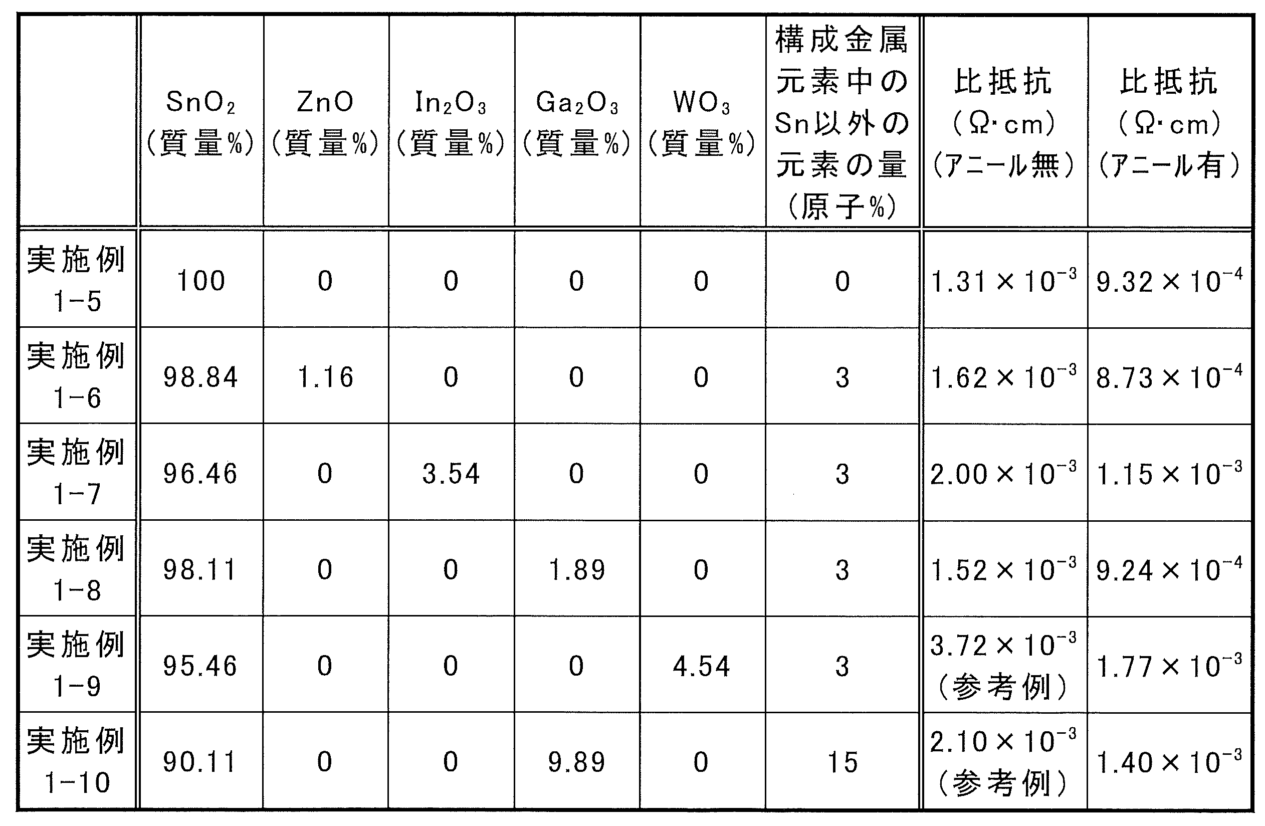
上記表3に示されるように、金属酸化物を構成する金属元素として、Sn以外の元素(Zn、InまたはGa)を3原子%含む場合にも、比抵抗を2×10⁻³Ω・cm以下とできた。また、いずれの透明導電膜においても、アニールによって、比抵抗がより小さくなった(実施例1-5~1-8)。なお、金属酸化物を構成する金属元素として、Wを3原子%含む場合には、アニール無しでは、比抵抗が2×10⁻³を超えたが、アニールによって、比抵抗を2×10⁻³Ω・cm以下とできた。
本発明の透明導電膜を、受光側透明電極および/または裏側透明電極に用い、フロントジャンクションSiヘテロ接合型太陽電池を作製した。当該太陽電池の外部量子効率と、ITO膜を受光側透明電極および裏側透明電極に用いた、従来型のSiヘテロ接合型太陽電池の外部量子効率とを比較し、評価を行った。
・光電変換層の準備
両表面が(100)面である、厚み280μm、かつ比抵抗が2Ωcmであるn型単結晶シリコン基板を準備した。当該n型単結晶シリコン基板の表面を、KOHを主成分とする溶液でウェットエッチングし、n型単結晶シリコン基板の両面に(111)ファセット面からなるランダムテクスチャ構造を形成した。
続いて、希フッ酸により、n型単結晶シリコン基板の両面の自然酸化膜を除去した。そして、n型単結晶シリコン基板の裏面側に、i型のa-Si:H層(厚み5nm程度)およびn型のa-Si:H層(厚み7nm程度)をプラズマ支援化学気相堆積法(PECVD)法で作製した。さらに、n型単結晶シリコン基板の受光面側にi型のa-Si:H層(厚み5nm程度)およびp型のa-Si:H層(厚み5nm程度)をPECVD法で作製した。これにより、受光面側から、p型a-Si:H層/i型a-Si:H層/n型単結晶シリコン層/i型a-Si:H層/n型a-Si:H層がこの順に積層された光電変換層を得た。
上記光電変換層の両面に、上述の実施例1-1と同様の方法で、非晶質SnO2膜からなる透明電極を形成した。これらの厚みは、それぞれ75nmとした。さらに、受光面側の透明導電膜(受光側透明電極)上に、スパッタリング法により、Agからなるグリッド電極(幅100μm、厚み2μm)を作製した。裏面側の透明導電膜(裏側透明電極上)には、スパッタリング法により、Agからなる金属電極を全面に形成した。その後、160℃にてアニール処理を行って、フロントジャンクションSiヘテロ接合型太陽電池を得た。
受光面側の透明電極を非晶質SnO2膜(厚み75nm)とし、裏面側の透明電極をITO膜(厚み75nm、スパッタリング法で作製)とした以外は、上記実施例2-1と同様にフロントジャンクションSiヘテロ接合型太陽電池を得た。
受光面側および裏面側の透明電極を、それぞれITO膜(厚み75nm、スパッタリング法で作製)とした以外は、上記実施例2-1と同様にフロントジャンクションSiヘテロ接合型太陽電池を得た。
実施例2-1および2-2、ならびに参考例2で得られたフロントジャンクションSiヘテロ接合型太陽電池の外部量子効率スペクトルを図8に示す。図8に示すように、受光面側/裏面側の透明電極を非晶質SnO2膜/非晶質SnO2膜とした実施例2-1の太陽電池や、受光面側/裏面側の透明電極を非晶質SnO2膜/ITO膜とした実施例2-2の太陽電池の外部量子効率は、従来型(参考例2)の太陽電池の外部量子効率と比較して遜色がなかった。
本発明の透明導電膜を、受光側透明電極および/または裏側透明電極に用いたリアジャンクションSiヘテロ接合型太陽電池を作製した。当該太陽電池の電流-電圧特性と、ITO膜を受光側透明電極および裏側透明電極に用いた、従来型のリアジャンクションSiヘテロ接合型太陽電池の電流-電圧特性とを比較し、評価を行った。
光電変換層を受光面側から、n型a-Si:H層/i型a-Si:H層/n型単結晶シリコン層/i型a-Si:H層/p型a-Si:H層とした以外は、実施例2-1と同様の工程を行い、リアジャンクションSiヘテロ接合型太陽電池を作製した。
受光面側の透明電極を非晶質SnO2膜(厚み75nm)とし、裏面側の透明電極をITO膜(厚み75nm、スパッタリング法で作製)とした以外は、上記実施例3-1と同様に、リアジャンクションSiヘテロ接合型太陽電池を得た。
受光面側および裏面側の透明電極を、それぞれITO膜(厚み75nm、スパッタリング法で作製)とした以外は、実施例3-1と同様にリアジャンクションSiヘテロ接合型太陽電池を得た。
光電変換層のn型a-Si:H膜を、n型nc-SiOx:H膜(厚み10nm)に変更した以外は、実施例3-2と同様に、リアジャンクションSiヘテロ接合型太陽電池を得た。
実施例3-1および3-2、ならびに参考例3で得られたリアジャンクションSiヘテロ接合型太陽電池の電流-電圧特性を図9に示す。本発明の透明導電膜を受光側透明電極および/または裏側透明電極に用いた実施例3-1および実施例3-2の太陽電池では、良好な電流-電圧特性を示したものの、従来型の太陽電池(参考例3)と比較すると、直列抵抗の増加に伴い、曲線因子(FF)が低下した。
上述の結果を受け、曲線因子(FF)の低下要因を明らかにするため、n型およびp型コンタクト構造のコンタクト抵抗をTLM(transmission line measurement)法にて評価した。n型およびp型コンタクト抵抗評価サンプルは、それぞれ、リアジャンクションおよびフロントジャンクション型Siヘテロ接合型太陽電池の光入射側と全く同一の層構造とした。すなわち、n型コンタクト抵抗評価サンプルは、Ag/透明導電膜/n型半導体層/i型a-Si:H層/n型結晶シリコン層で構成され、当該n型コンタクト抵抗評価サンプルによって、リアジャンクション型Siヘテロ接合型太陽電池の光入射側n型コンタクト構造の直列抵抗を評価した。また、p型コンタクト抵抗評価サンプルは、Ag/透明導電膜/p型半導体層/i型a-Si:H層/p型結晶シリコン層で構成され、当該p型コンタクト抵抗評価サンプルによって、フロントジャンクション型Siヘテロ接合型太陽電池の光入射側p型コンタクト構造の直列抵抗を評価した。コンタクト抵抗評価サンプルと太陽電池との相違点は、電極となるAg/透明導電膜の積層部が短冊形状にパターン化されている点、およびp型コンタクト抵抗評価サンプルではp型結晶シリコンを用いる点の2つである。フロントジャンクションSiヘテロ型太陽電池(実施例2-2の構成)のp型コンタクト構造について、本発明の透明導電膜(a-SnO2膜)に隣接する半導体層の種類を変更したコンタクト抵抗評価サンプル(下記の実施例2-2a)を作製し、コンタクト抵抗値を評価した。さらに、従来型のITO膜を用いた太陽電池(参考例2および3)のp型コンタクト構造についても、ITO膜に隣接する半導体層の種類を変更したコンタクト抵抗評価サンプル(下記の参考例2aおよび3a)を作製し、そのコンタクト抵抗値を確認した。
光電変換層のp型a-Si:H層を、p型nc-Si:H層(厚み20nm)に変更した以外は、実施例2-2と同様の構造を持つ、p型コンタクト抵抗評価サンプルを得た。
光電変換層のp型a-Si:H層を、p型nc-Si:H層(厚み20nm)に変更した以外は、参考例2と同様の構造を持つ、p型コンタクト抵抗評価サンプルを得た。
光電変換層のn型a-Si:H層を、n型nc-SiOx:H層(厚み10nm)に変更した以外は、参考例3と同様の構造を持つ、n型コンタクト抵抗評価サンプルを得た。
実施例3-2a、参考例3a、実施例3-2、および参考例3で作製したリアジャンクションSiヘテロ接合型太陽電池の光入射側のコンタクト構造に相当する、各n型コンタクト構造(Ag/透明導電膜/n型半導体層/i型a-Si:H層/n型結晶シリコン層)のコンタクト抵抗値を図11に示す。同様に、実施例2-2a、参考例2a、実施例2-2、および参考例2で得られたフロントジャンクションSiヘテロ接合型太陽電池の光入射側のコンタクト構造に相当する、各p型コンタクト構造(Ag/透明導電膜/p型半導体層/i型a-Si:H層/p型結晶シリコン層)のコンタクト抵抗値も図11に示す。図11から明らかなように、フロントジャンクション型(光入射側がp型コンタクト)、リアジャンクション型(光入射側がn型コンタクト)のいずれの構成においても、本発明の透明導電膜(a-SnO2膜)に隣接する半導体層を、a-Si:H層からnc-Si:H層またはnc-SiOx:Hに変更することで、直列抵抗値が格段に低下した(実施例3-2aおよび実施例2-2a)。また、このような構成とすることで、従来型の太陽電池(参考例3および参考例2)と同等、もしくは従来型より低い直列抵抗値とすることができた。
RFマグネトロンスパッタ法により、以下の方法で透明導電膜を作製した。まず、基板として無アルカリガラス基板(コーニング社製XG)(寸法50mm×50mm)を準備した。さらに、ターゲットとして3インチφのSnO2焼結体を準備し、基板温度を非加熱(室温)とした。スパッタ装置内にArガスとO2ガスとを導入し、酸素流量比0.25%あるいは0.375%とし、チャンバー圧力を0.5Paとした。そして、スパッタ投入電力100Wにて、それぞれ20分成膜を行い、厚み70nmの透明導電膜(SnO2膜)を得た。得られた透明導電膜を、窒素雰囲気下、200℃で0.5時間アニール処理した。
(実施例a1)
基板として、PI(ポリイミド)基板(厚さ125μm、寸法100mm×100mm)を準備した。そして、当該PI基板上に、実施例1-1と同様の条件にて、反応性プラズマ堆積法により、非晶質SnO2を主成分とする透明導電膜を作製した。得られた透明導電膜のシート抵抗はロレスタ(低抵抗率計)により測定した。このときの膜厚、シート抵抗、および比抵抗をそれぞれ表4に示す。なお、表4には記載しないが、透明導電膜の組成を実施例1―1と同様にICP分析法で確認したところ、構成する金属元素はSnのみであり、Inは定量下限以下であった。
実施例(a1)で作製した透明導電膜付基板を、250℃で0.5時間アニール処理した。このときのシート抵抗、および比抵抗を表4に示す。
PI基板上に、反応性プラズマ堆積法により、In2O3系透明導電膜の一つであるCeとHとを添加したIn2O3:Ce,H透明導電膜を堆積した。その後、実施例a1と同様に非晶質SnO2を主成分とする透明導電膜を作製した。各透明導電膜の膜厚、シート抵抗、および比抵抗を表4に示す。なお、表4に示す比抵抗は、各透明導電膜の電気特性が膜厚方向に均一であると仮定した場合の比抵抗(参考データ)である。また表4には記載しないが、非晶質SnO2を主成分とする透明導電膜を構成する金属元素はSnのみであり、Inは定量下限以下であった。さらに、表4には記載しないが、非晶質SnO2を主成分とする透明導電膜のみの比抵抗が、2×10⁻³Ω・cm以下であることは、実施例a1の比抵抗から明らかである。
上記実施例a3、a5、a7、およびa9で作製した透明導電膜付基板を、それぞれ250℃で0.5時間アニール処理した。このときのシート抵抗、および比抵抗を表4に示す。
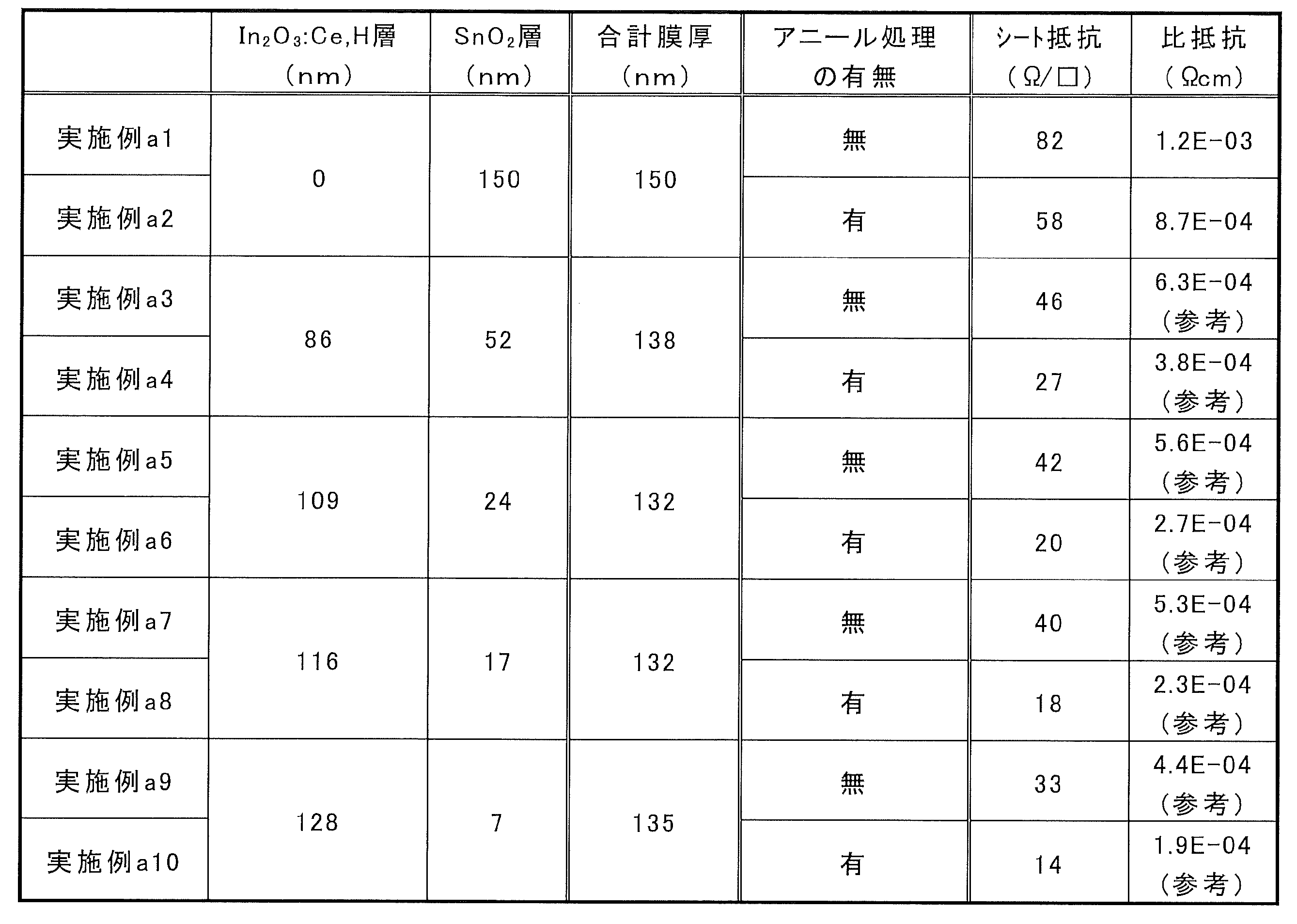
上記表4に示すように、In2O3:Ce,H透明導電膜の上に非晶質SnO2を主成分とする透明導電膜を積層した場合、In2O3:Ce,H透明導電膜の割合を増加させることにより、透明導電膜付基板のシート抵抗が単調に減少した(実施例a3~a10)。つまり、公知の透明導電膜(In2O3:Ce,H膜)を有する基板に、さらに本発明の透明導電膜(非晶質SnO2膜)を積層することで、非常に有用な透明導電膜付基板が得られることが確認された。
(実施例b1、b3、b5、およびb7)
基板として、PI(ポリイミド)基板(厚さ125μm、寸法100mm×100mm)を準備した。その後、実施例1-1と同様の条件にて、反応性プラズマ堆積法により、非晶質SnO2を主成分とする透明導電膜を作製した。次いで、当該透明導電膜(非晶質SnO2)上に、実施例a3と同様に、反応性プラズマ堆積法によりIn2O3:Ce,H透明導電膜を堆積した。さらに実施例1-1と同様の条件にて、反応性プラズマ堆積法により、非晶質SnO2を主成分とする透明導電膜を作製した。各透明導電膜の膜厚、シート抵抗、および比抵抗を表5に示す。なお、表5に示す比抵抗は、各透明導電膜の電気特性が膜厚方向に均一であると仮定した場合の比抵抗(参考データ)である。また、表5には記載しないが、非晶質SnO2を主成分とする透明導電膜を構成する金属元素はSnのみであり、Inは定量下限以下であった。さらに、表5には記載しないが、非晶質SnO2を主成分とする透明導電膜のみの比抵抗が、2×10⁻³Ω・cm以下であることは、上述の実施例a1の比抵抗から明らかである。
実施例b1、b3、b5、およびb7で作製した透明導電膜付基板を、250℃で0.5時間アニール処理した。このときのシート抵抗、および比抵抗を表5に示す。
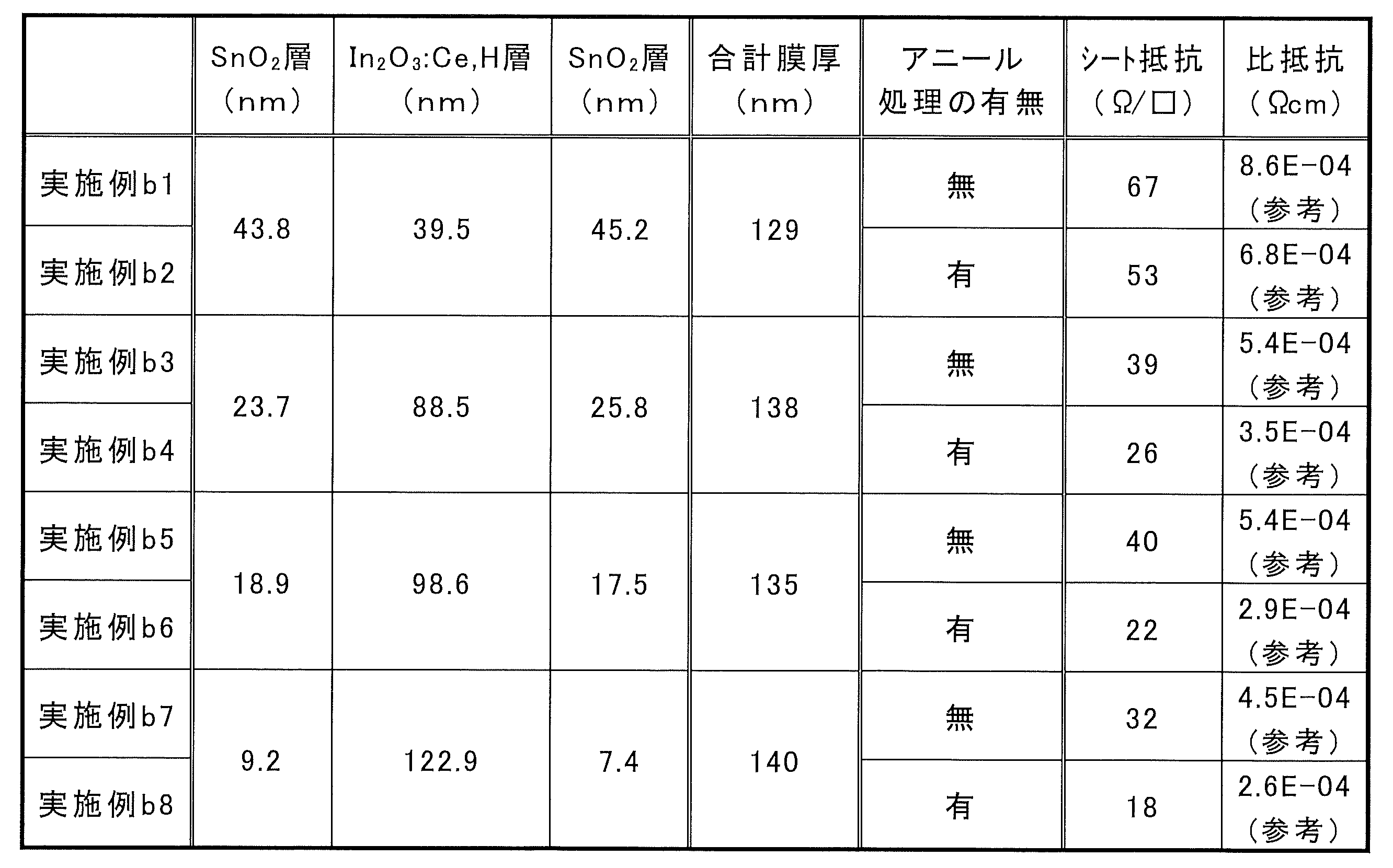
上記表5に示すように、非晶質SnO2を主成分とする透明導電膜/In2O3:Ce,H膜/非晶質SnO2を主成分とする透明導電膜を積層した場合、In2O3:Ce,H膜の割合を増加させることにより、透明導電膜付基板のシート抵抗が単調に減少した。つまり、本発明の透明導電膜(非晶質SnO2膜)と、公知の透明導電膜(In2O3:Ce,H膜)とを積層することで、非常に有用な透明導電膜付基板が得られることが確認された。
10 ハース部
11 材料
20 プラズマガン
21 プラズマビーム
22 プラズマ
30 プラズマコントローラ
40 チャンバー
100 反応性プラズマ堆積装置
120 n型単結晶シリコン層
121、123 i型半導体層
122 p型半導体層
124 n型半導体層
125 受光側透明電極
126 グリッド電極
127 裏側透明電極
128 金属電極
130 光電変換層
131 第1電極
132 第2電極
200 Siヘテロ接合型太陽電池
400 ペロブスカイト型太陽電池
Claims (9)
- 非晶質の酸化錫が主成分である金属酸化物を含み、
前記金属酸化物を構成する金属元素のうちSnの量が85原子%以上であり、Inの量が4原子%以下であり、かつ
比抵抗が2×10⁻³Ω・cm以下である、透明導電膜。 - 波長420nm以上500nm以下における、最大吸収係数が1×104cm-1以下である、
請求項1に記載の透明導電膜。 - In、Zn、Cd、Nb、Ta、B、Ga、Ba、Mo、Pb、Rb、Re、Sb、W、Ce、Cs、Dy、Er、Ge、Hf、Ho、La、Lu、Nd、Pr、Sc、Si、Sm、Tb、V、Y、Al、Ti、Zr、Siからなる群から選ばれる少なくとも一種を含む、
請求項1に記載の透明導電膜。 - 二次イオン質量分析法で測定される、両表面からそれぞれ10nm以上内側の領域における水素原子の濃度が、8×10²¹原子/cm3以下である、
請求項1に記載の透明導電膜。 - 基板と、
前記基板上に配置された、請求項1~4のいずれか一項に記載の透明導電膜と、
を含む、透明導電膜付基板。 - 前記基板が、樹脂フィルムである。
請求項5に記載の透明導電膜付基板。 - 光電変換層と、
前記光電変換層に隣接して配置された、少なくとも一層の導電膜を含む第1電極と、
前記光電変換層に隣接して配置された、少なくとも一層の導電膜を含む第2電極と、
を有し、
前記第1電極および前記第2電極の少なくとも一方が、請求項1~4のいずれか一項に記載の透明導電膜を含む、
光電変換素子。 - 前記光電変換素子が太陽電池であり、
前記光電変換層が、n型またはp型にドープされた単結晶シリコン層と、前記単結晶シリコン層の一方の側に配置されたp型半導体層と、前記単結晶シリコン層の他方の側または同じ側に配置されたn型半導体層と、を含む、
請求項7に記載の光電変換素子。 - 前記p型半導体層が、p型微結晶シリコン層またはその合金層である、および/または前記n型半導体層が、n型微結晶シリコン層またはその合金層であり、
前記透明導電膜が、前記p型微結晶シリコン層またはその合金層および/または前記n型微結晶シリコン層またはその合金層に隣接して配置されている、
請求項8に記載の光電変換素子。
Priority Applications (2)
| Application Number | Priority Date | Filing Date | Title |
|---|---|---|---|
| CN202480013806.6A CN120752709A (zh) | 2023-02-22 | 2024-02-06 | 透明导电膜、带透明导电膜的基板及光电转换元件 |
| JP2025502236A JPWO2024176803A1 (ja) | 2023-02-22 | 2024-02-06 |
Applications Claiming Priority (2)
| Application Number | Priority Date | Filing Date | Title |
|---|---|---|---|
| JP2023-026205 | 2023-02-22 | ||
| JP2023026205 | 2023-02-22 |
Publications (1)
| Publication Number | Publication Date |
|---|---|
| WO2024176803A1 true WO2024176803A1 (ja) | 2024-08-29 |
Family
ID=92500606
Family Applications (1)
| Application Number | Title | Priority Date | Filing Date |
|---|---|---|---|
| PCT/JP2024/003815 Ceased WO2024176803A1 (ja) | 2023-02-22 | 2024-02-06 | 透明導電膜、透明導電膜付基板、および光電変換素子 |
Country Status (3)
| Country | Link |
|---|---|
| JP (1) | JPWO2024176803A1 (ja) |
| CN (1) | CN120752709A (ja) |
| WO (1) | WO2024176803A1 (ja) |
Citations (5)
| Publication number | Priority date | Publication date | Assignee | Title |
|---|---|---|---|---|
| JP2000256059A (ja) * | 1999-03-05 | 2000-09-19 | Idemitsu Kosan Co Ltd | 透明導電材料、透明導電ガラス及び透明導電フィルム |
| JP2007314364A (ja) * | 2006-05-24 | 2007-12-06 | Sumitomo Metal Mining Co Ltd | 酸化物焼結体、ターゲット、及びそれを用いて得られる酸化物透明導電膜ならびにその製造方法 |
| JP2019009402A (ja) * | 2017-06-28 | 2019-01-17 | 国立研究開発法人物質・材料研究機構 | 太陽電池およびその製造方法 |
| WO2019188716A1 (ja) * | 2018-03-29 | 2019-10-03 | 株式会社カネカ | 太陽電池およびその製造方法 |
| JP2020167238A (ja) * | 2019-03-28 | 2020-10-08 | パナソニック株式会社 | 太陽電池セルおよび太陽電池モジュール |
-
2024
- 2024-02-06 JP JP2025502236A patent/JPWO2024176803A1/ja active Pending
- 2024-02-06 WO PCT/JP2024/003815 patent/WO2024176803A1/ja not_active Ceased
- 2024-02-06 CN CN202480013806.6A patent/CN120752709A/zh active Pending
Patent Citations (5)
| Publication number | Priority date | Publication date | Assignee | Title |
|---|---|---|---|---|
| JP2000256059A (ja) * | 1999-03-05 | 2000-09-19 | Idemitsu Kosan Co Ltd | 透明導電材料、透明導電ガラス及び透明導電フィルム |
| JP2007314364A (ja) * | 2006-05-24 | 2007-12-06 | Sumitomo Metal Mining Co Ltd | 酸化物焼結体、ターゲット、及びそれを用いて得られる酸化物透明導電膜ならびにその製造方法 |
| JP2019009402A (ja) * | 2017-06-28 | 2019-01-17 | 国立研究開発法人物質・材料研究機構 | 太陽電池およびその製造方法 |
| WO2019188716A1 (ja) * | 2018-03-29 | 2019-10-03 | 株式会社カネカ | 太陽電池およびその製造方法 |
| JP2020167238A (ja) * | 2019-03-28 | 2020-10-08 | パナソニック株式会社 | 太陽電池セルおよび太陽電池モジュール |
Also Published As
| Publication number | Publication date |
|---|---|
| CN120752709A (zh) | 2025-10-03 |
| JPWO2024176803A1 (ja) | 2024-08-29 |
Similar Documents
| Publication | Publication Date | Title |
|---|---|---|
| Kim et al. | Transparent conducting F-doped SnO2 thin films grown by pulsed laser deposition | |
| EP3719853B1 (en) | Thin-film photovoltaic devices including cadmium and tellurium doped with group v elements | |
| JP4556407B2 (ja) | 酸化物透明電極膜とその製造方法、透明導電性基材、太陽電池および光検出素子 | |
| US7875945B2 (en) | Rear electrode structure for use in photovoltaic device such as CIGS/CIS photovoltaic device and method of making same | |
| KR101000057B1 (ko) | 다층 투명전도층을 구비한 태양전지 이의 제조방법 | |
| EP2530722A2 (en) | Refractive index matching of thin film layers for photovoltaic devices and methods of their manufacture | |
| US20080308147A1 (en) | Rear electrode structure for use in photovoltaic device such as CIGS/CIS photovoltaic device and method of making same | |
| US20090194165A1 (en) | Ultra-high current density cadmium telluride photovoltaic modules | |
| US20110061730A1 (en) | Textured rear electrode structure for use in photovoltaic device such as CIGS/CIS solar cell | |
| KR20100094988A (ko) | 광을 수집할 수 있는 요소의 개선 | |
| US20140000690A1 (en) | Intrinsically Semitransparent Solar Cell and Method of Making Same | |
| TW201222843A (en) | Transparent electrically conductive substrate carrying thereon a surface electrode, a manufacturing method therefor, a thin-film solar cell and a manufacturing method therefor | |
| US8354586B2 (en) | Transparent conductor film stack with cadmium stannate, corresponding photovoltaic device, and method of making same | |
| AU2009316838A1 (en) | Photovoltaic devices including heterojunctions | |
| US20170104108A1 (en) | Doping an absorber layer of a photovoltaic device via diffusion from a window layer | |
| JPWO2006057160A1 (ja) | 薄膜光電変換装置 | |
| CN107615494B (zh) | 氧化物透明导电膜、光电转换元件以及光电转换元件的制造方法 | |
| US20130109124A1 (en) | Methods of making a transparent layer and a photovoltaic device | |
| JP5243697B2 (ja) | 光電変換装置用透明導電膜とその製造方法 | |
| TW201246277A (en) | Method of manufacturing transparent conductive substrate with surface electrode and method of manufacturing thin film solar cell | |
| US20130153024A1 (en) | Multilayer transparent electroconductive film and method for manufacturing same, as well as thin-film solar cell and method for manufacturing same | |
| US9034686B2 (en) | Manufacturing methods for semiconductor devices | |
| CN120752709A (zh) | 透明导电膜、带透明导电膜的基板及光电转换元件 | |
| CN101246918A (zh) | 非晶硅光伏器件中的防反射膜 | |
| JP5563850B2 (ja) | 光電変換装置およびその製造方法 |
Legal Events
| Date | Code | Title | Description |
|---|---|---|---|
| 121 | Ep: the epo has been informed by wipo that ep was designated in this application |
Ref document number: 24760109 Country of ref document: EP Kind code of ref document: A1 |
|
| ENP | Entry into the national phase |
Ref document number: 2025502236 Country of ref document: JP Kind code of ref document: A |
|
| WWE | Wipo information: entry into national phase |
Ref document number: 2025502236 Country of ref document: JP |
|
| WWE | Wipo information: entry into national phase |
Ref document number: 202480013806.6 Country of ref document: CN |
|
| NENP | Non-entry into the national phase |
Ref country code: DE |
|
| WWP | Wipo information: published in national office |
Ref document number: 202480013806.6 Country of ref document: CN |
|
| 122 | Ep: pct application non-entry in european phase |
Ref document number: 24760109 Country of ref document: EP Kind code of ref document: A1 |