WO2024176751A1 - 半導体装置および車両 - Google Patents
半導体装置および車両 Download PDFInfo
- Publication number
- WO2024176751A1 WO2024176751A1 PCT/JP2024/002755 JP2024002755W WO2024176751A1 WO 2024176751 A1 WO2024176751 A1 WO 2024176751A1 JP 2024002755 W JP2024002755 W JP 2024002755W WO 2024176751 A1 WO2024176751 A1 WO 2024176751A1
- Authority
- WO
- WIPO (PCT)
- Prior art keywords
- layer
- electrode
- semiconductor device
- wiring layer
- center
- Prior art date
- Legal status (The legal status is an assumption and is not a legal conclusion. Google has not performed a legal analysis and makes no representation as to the accuracy of the status listed.)
- Ceased
Links
Images














Classifications
-
- H—ELECTRICITY
- H10—SEMICONDUCTOR DEVICES; ELECTRIC SOLID-STATE DEVICES NOT OTHERWISE PROVIDED FOR
- H10W—GENERIC PACKAGES, INTERCONNECTIONS, CONNECTORS OR OTHER CONSTRUCTIONAL DETAILS OF DEVICES COVERED BY CLASS H10
- H10W72/00—Interconnections or connectors in packages
- H10W72/90—Bond pads, in general
-
- H—ELECTRICITY
- H10—SEMICONDUCTOR DEVICES; ELECTRIC SOLID-STATE DEVICES NOT OTHERWISE PROVIDED FOR
- H10W—GENERIC PACKAGES, INTERCONNECTIONS, CONNECTORS OR OTHER CONSTRUCTIONAL DETAILS OF DEVICES COVERED BY CLASS H10
- H10W20/00—Interconnections in chips, wafers or substrates
- H10W20/40—Interconnections external to wafers or substrates, e.g. back-end-of-line [BEOL] metallisations or vias connecting to gate electrodes
- H10W20/41—Interconnections external to wafers or substrates, e.g. back-end-of-line [BEOL] metallisations or vias connecting to gate electrodes characterised by their conductive parts
- H10W20/43—Layouts of interconnections
-
- H—ELECTRICITY
- H10—SEMICONDUCTOR DEVICES; ELECTRIC SOLID-STATE DEVICES NOT OTHERWISE PROVIDED FOR
- H10W—GENERIC PACKAGES, INTERCONNECTIONS, CONNECTORS OR OTHER CONSTRUCTIONAL DETAILS OF DEVICES COVERED BY CLASS H10
- H10W20/00—Interconnections in chips, wafers or substrates
- H10W20/40—Interconnections external to wafers or substrates, e.g. back-end-of-line [BEOL] metallisations or vias connecting to gate electrodes
- H10W20/41—Interconnections external to wafers or substrates, e.g. back-end-of-line [BEOL] metallisations or vias connecting to gate electrodes characterised by their conductive parts
- H10W20/44—Conductive materials thereof
- H10W20/4403—Conductive materials thereof based on metals, e.g. alloys, metal silicides
- H10W20/4421—Conductive materials thereof based on metals, e.g. alloys, metal silicides the principal metal being copper
-
- H—ELECTRICITY
- H10—SEMICONDUCTOR DEVICES; ELECTRIC SOLID-STATE DEVICES NOT OTHERWISE PROVIDED FOR
- H10W—GENERIC PACKAGES, INTERCONNECTIONS, CONNECTORS OR OTHER CONSTRUCTIONAL DETAILS OF DEVICES COVERED BY CLASS H10
- H10W74/00—Encapsulations, e.g. protective coatings
- H10W74/10—Encapsulations, e.g. protective coatings characterised by their shape or disposition
- H10W74/111—Encapsulations, e.g. protective coatings characterised by their shape or disposition the semiconductor body being completely enclosed
- H10W74/114—Encapsulations, e.g. protective coatings characterised by their shape or disposition the semiconductor body being completely enclosed by a substrate and the encapsulations
-
- H—ELECTRICITY
- H10—SEMICONDUCTOR DEVICES; ELECTRIC SOLID-STATE DEVICES NOT OTHERWISE PROVIDED FOR
- H10W—GENERIC PACKAGES, INTERCONNECTIONS, CONNECTORS OR OTHER CONSTRUCTIONAL DETAILS OF DEVICES COVERED BY CLASS H10
- H10W90/00—Package configurations
-
- H—ELECTRICITY
- H10—SEMICONDUCTOR DEVICES; ELECTRIC SOLID-STATE DEVICES NOT OTHERWISE PROVIDED FOR
- H10D—INORGANIC ELECTRIC SEMICONDUCTOR DEVICES
- H10D80/00—Assemblies of multiple devices comprising at least one device covered by this subclass
- H10D80/20—Assemblies of multiple devices comprising at least one device covered by this subclass the at least one device being covered by groups H10D1/00 - H10D48/00, e.g. assemblies comprising capacitors, power FETs or Schottky diodes
- H10D80/251—FETs covered by H10D30/00, e.g. power FETs
-
- H—ELECTRICITY
- H10—SEMICONDUCTOR DEVICES; ELECTRIC SOLID-STATE DEVICES NOT OTHERWISE PROVIDED FOR
- H10W—GENERIC PACKAGES, INTERCONNECTIONS, CONNECTORS OR OTHER CONSTRUCTIONAL DETAILS OF DEVICES COVERED BY CLASS H10
- H10W72/00—Interconnections or connectors in packages
- H10W72/071—Connecting or disconnecting
- H10W72/073—Connecting or disconnecting of die-attach connectors
- H10W72/07331—Connecting techniques
- H10W72/07336—Soldering or alloying
-
- H—ELECTRICITY
- H10—SEMICONDUCTOR DEVICES; ELECTRIC SOLID-STATE DEVICES NOT OTHERWISE PROVIDED FOR
- H10W—GENERIC PACKAGES, INTERCONNECTIONS, CONNECTORS OR OTHER CONSTRUCTIONAL DETAILS OF DEVICES COVERED BY CLASS H10
- H10W72/00—Interconnections or connectors in packages
- H10W72/071—Connecting or disconnecting
- H10W72/073—Connecting or disconnecting of die-attach connectors
- H10W72/07351—Connecting or disconnecting of die-attach connectors characterised by changes in properties of the die-attach connectors during connecting
- H10W72/07354—Connecting or disconnecting of die-attach connectors characterised by changes in properties of the die-attach connectors during connecting changes in dispositions
-
- H—ELECTRICITY
- H10—SEMICONDUCTOR DEVICES; ELECTRIC SOLID-STATE DEVICES NOT OTHERWISE PROVIDED FOR
- H10W—GENERIC PACKAGES, INTERCONNECTIONS, CONNECTORS OR OTHER CONSTRUCTIONAL DETAILS OF DEVICES COVERED BY CLASS H10
- H10W72/00—Interconnections or connectors in packages
- H10W72/30—Die-attach connectors
- H10W72/341—Dispositions of die-attach connectors, e.g. layouts
- H10W72/347—Dispositions of multiple die-attach connectors
-
- H—ELECTRICITY
- H10—SEMICONDUCTOR DEVICES; ELECTRIC SOLID-STATE DEVICES NOT OTHERWISE PROVIDED FOR
- H10W—GENERIC PACKAGES, INTERCONNECTIONS, CONNECTORS OR OTHER CONSTRUCTIONAL DETAILS OF DEVICES COVERED BY CLASS H10
- H10W72/00—Interconnections or connectors in packages
- H10W72/30—Die-attach connectors
- H10W72/351—Materials of die-attach connectors
- H10W72/352—Materials of die-attach connectors comprising metals or metalloids, e.g. solders
-
- H—ELECTRICITY
- H10—SEMICONDUCTOR DEVICES; ELECTRIC SOLID-STATE DEVICES NOT OTHERWISE PROVIDED FOR
- H10W—GENERIC PACKAGES, INTERCONNECTIONS, CONNECTORS OR OTHER CONSTRUCTIONAL DETAILS OF DEVICES COVERED BY CLASS H10
- H10W72/00—Interconnections or connectors in packages
- H10W72/50—Bond wires
- H10W72/541—Dispositions of bond wires
- H10W72/5445—Dispositions of bond wires being orthogonal to a side surface of the chip, e.g. parallel arrangements
-
- H—ELECTRICITY
- H10—SEMICONDUCTOR DEVICES; ELECTRIC SOLID-STATE DEVICES NOT OTHERWISE PROVIDED FOR
- H10W—GENERIC PACKAGES, INTERCONNECTIONS, CONNECTORS OR OTHER CONSTRUCTIONAL DETAILS OF DEVICES COVERED BY CLASS H10
- H10W72/00—Interconnections or connectors in packages
- H10W72/50—Bond wires
- H10W72/541—Dispositions of bond wires
- H10W72/547—Dispositions of multiple bond wires
- H10W72/5475—Dispositions of multiple bond wires multiple bond wires connected to common bond pads at both ends of the wires
-
- H—ELECTRICITY
- H10—SEMICONDUCTOR DEVICES; ELECTRIC SOLID-STATE DEVICES NOT OTHERWISE PROVIDED FOR
- H10W—GENERIC PACKAGES, INTERCONNECTIONS, CONNECTORS OR OTHER CONSTRUCTIONAL DETAILS OF DEVICES COVERED BY CLASS H10
- H10W72/00—Interconnections or connectors in packages
- H10W72/50—Bond wires
- H10W72/551—Materials of bond wires
-
- H—ELECTRICITY
- H10—SEMICONDUCTOR DEVICES; ELECTRIC SOLID-STATE DEVICES NOT OTHERWISE PROVIDED FOR
- H10W—GENERIC PACKAGES, INTERCONNECTIONS, CONNECTORS OR OTHER CONSTRUCTIONAL DETAILS OF DEVICES COVERED BY CLASS H10
- H10W72/00—Interconnections or connectors in packages
- H10W72/851—Dispositions of multiple connectors or interconnections
- H10W72/853—On the same surface
- H10W72/871—Bond wires and strap connectors
-
- H—ELECTRICITY
- H10—SEMICONDUCTOR DEVICES; ELECTRIC SOLID-STATE DEVICES NOT OTHERWISE PROVIDED FOR
- H10W—GENERIC PACKAGES, INTERCONNECTIONS, CONNECTORS OR OTHER CONSTRUCTIONAL DETAILS OF DEVICES COVERED BY CLASS H10
- H10W72/00—Interconnections or connectors in packages
- H10W72/851—Dispositions of multiple connectors or interconnections
- H10W72/874—On different surfaces
- H10W72/884—Die-attach connectors and bond wires
-
- H—ELECTRICITY
- H10—SEMICONDUCTOR DEVICES; ELECTRIC SOLID-STATE DEVICES NOT OTHERWISE PROVIDED FOR
- H10W—GENERIC PACKAGES, INTERCONNECTIONS, CONNECTORS OR OTHER CONSTRUCTIONAL DETAILS OF DEVICES COVERED BY CLASS H10
- H10W72/00—Interconnections or connectors in packages
- H10W72/851—Dispositions of multiple connectors or interconnections
- H10W72/874—On different surfaces
- H10W72/886—Die-attach connectors and strap connectors
-
- H—ELECTRICITY
- H10—SEMICONDUCTOR DEVICES; ELECTRIC SOLID-STATE DEVICES NOT OTHERWISE PROVIDED FOR
- H10W—GENERIC PACKAGES, INTERCONNECTIONS, CONNECTORS OR OTHER CONSTRUCTIONAL DETAILS OF DEVICES COVERED BY CLASS H10
- H10W72/00—Interconnections or connectors in packages
- H10W72/90—Bond pads, in general
- H10W72/921—Structures or relative sizes of bond pads
- H10W72/926—Multiple bond pads having different sizes
-
- H—ELECTRICITY
- H10—SEMICONDUCTOR DEVICES; ELECTRIC SOLID-STATE DEVICES NOT OTHERWISE PROVIDED FOR
- H10W—GENERIC PACKAGES, INTERCONNECTIONS, CONNECTORS OR OTHER CONSTRUCTIONAL DETAILS OF DEVICES COVERED BY CLASS H10
- H10W72/00—Interconnections or connectors in packages
- H10W72/90—Bond pads, in general
- H10W72/941—Dispositions of bond pads
- H10W72/9415—Dispositions of bond pads relative to the surface, e.g. recessed, protruding
-
- H—ELECTRICITY
- H10—SEMICONDUCTOR DEVICES; ELECTRIC SOLID-STATE DEVICES NOT OTHERWISE PROVIDED FOR
- H10W—GENERIC PACKAGES, INTERCONNECTIONS, CONNECTORS OR OTHER CONSTRUCTIONAL DETAILS OF DEVICES COVERED BY CLASS H10
- H10W74/00—Encapsulations, e.g. protective coatings
-
- H—ELECTRICITY
- H10—SEMICONDUCTOR DEVICES; ELECTRIC SOLID-STATE DEVICES NOT OTHERWISE PROVIDED FOR
- H10W—GENERIC PACKAGES, INTERCONNECTIONS, CONNECTORS OR OTHER CONSTRUCTIONAL DETAILS OF DEVICES COVERED BY CLASS H10
- H10W90/00—Package configurations
- H10W90/701—Package configurations characterised by the relative positions of pads or connectors relative to package parts
- H10W90/731—Package configurations characterised by the relative positions of pads or connectors relative to package parts of die-attach connectors
- H10W90/736—Package configurations characterised by the relative positions of pads or connectors relative to package parts of die-attach connectors between a chip and a stacked lead frame, conducting package substrate or heat sink
-
- H—ELECTRICITY
- H10—SEMICONDUCTOR DEVICES; ELECTRIC SOLID-STATE DEVICES NOT OTHERWISE PROVIDED FOR
- H10W—GENERIC PACKAGES, INTERCONNECTIONS, CONNECTORS OR OTHER CONSTRUCTIONAL DETAILS OF DEVICES COVERED BY CLASS H10
- H10W90/00—Package configurations
- H10W90/701—Package configurations characterised by the relative positions of pads or connectors relative to package parts
- H10W90/751—Package configurations characterised by the relative positions of pads or connectors relative to package parts of bond wires
- H10W90/756—Package configurations characterised by the relative positions of pads or connectors relative to package parts of bond wires between a chip and a stacked lead frame, conducting package substrate or heat sink
Definitions
- This disclosure relates to a semiconductor device and a vehicle equipped with the semiconductor device.
- the semiconductor device disclosed in Patent Document 1 includes multiple first semiconductor elements, multiple first connection wirings, a wiring layer, and a signal terminal.
- the multiple first semiconductor elements are switching elements. Each of the multiple first semiconductor elements is driven to turn on and off in response to a drive signal input to the gate electrode.
- the multiple first semiconductor elements are connected in parallel.
- the multiple first connection wirings are, for example, wires, and connect the gate electrodes of the multiple first semiconductor elements to the wiring layer.
- a signal terminal is connected to the wiring layer.
- the signal terminal is connected to each gate electrode of the multiple first semiconductor elements via the wiring layer and the multiple first connection wirings.
- the signal terminal supplies a drive signal for driving the multiple first semiconductor elements to each gate electrode of the multiple first semiconductor elements.
- a resonance phenomenon may occur when each of the multiple semiconductor elements is switched (driven on and off).
- the effect of this resonance phenomenon may cause the drive signals of the multiple semiconductor elements to oscillate.
- each of the multiple semiconductor elements may malfunction or each of the multiple semiconductor elements may be destroyed.
- An object of the present disclosure is to provide a semiconductor device that is an improvement over conventional semiconductor devices.
- an object of the present disclosure is to provide a semiconductor device that is capable of suppressing the resonance phenomenon that occurs when multiple semiconductor elements are operated in parallel.
- Another object of the present disclosure is to provide a vehicle equipped with the semiconductor device.
- the semiconductor device provided by the first aspect of the present disclosure includes a conductive layer having a mounting surface facing a first direction, a first semiconductor element having a first gate electrode located on the opposite side to the mounting surface in the first direction and bonded to the mounting surface, a second semiconductor element having a second gate electrode located on the opposite side to the mounting surface in the first direction and bonded to the mounting surface, and a first signal terminal conductive to each of the first gate electrode and the second gate electrode.
- the first gate electrode has a first center.
- the second gate electrode has a second center.
- the first signal terminal has a first contact.
- a first straight line length connecting the first center and the first contact is defined as L1.
- a second straight line length connecting the second center and the first contact is defined as L2.
- a first conductive path length from the first center to the first contact is defined as R1.
- a second conductive path length from the second center to the first contact is defined as R2.
- R2/R1 satisfies a relationship closer to 1 than L2/L1.
- the vehicle provided by the second aspect of the present disclosure includes a drive source and a semiconductor device.
- the semiconductor device is electrically connected to the drive source.
- the semiconductor device further includes a first wiring layer and a sealing resin covering the first semiconductor element and the second semiconductor element, in comparison with the semiconductor device provided by the first aspect of the present disclosure.
- Each of the first gate electrode, the second gate electrode, and the first signal terminal is electrically connected to the first wiring layer.
- the first signal terminal includes a portion exposed from the sealing resin.
- the above configuration makes it possible to suppress the resonance phenomenon that occurs when multiple semiconductor elements are operated in parallel in a semiconductor device.
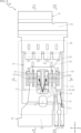
- FIG. 1 is a plan view of a semiconductor device according to a first embodiment of the present disclosure.
- FIG. 2 is a plan view corresponding to FIG. 1, seen through the sealing resin.
- FIG. 3 is a bottom view of the semiconductor device shown in FIG.
- FIG. 4 is a right side view of the semiconductor device shown in FIG.
- FIG. 5 is a cross-sectional view taken along line VV in FIG.
- FIG. 6 is a cross-sectional view taken along line VI-VI in FIG.
- FIG. 7 is a cross-sectional view taken along line VII-VII in FIG.
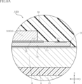
- FIG. 8A is a partially enlarged view of FIG. 5, showing the first semiconductor element and its vicinity.
- FIG. 8B is a partially enlarged view of FIG. 5, showing the second semiconductor element and its vicinity.
- FIG. 8A is a partially enlarged view of FIG. 5, showing the first semiconductor element and its vicinity.
- FIG. 8B is a partially enlarged view of FIG. 5, showing the second semiconductor element and its vicinity.
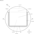
- FIG. 9 is a partially enlarged view of FIG.
- FIG. 10 is a cross-sectional view taken along line XX in FIG.
- FIG. 11 is a partially enlarged cross-sectional view of a semiconductor device according to a first modified example of the first embodiment of the present disclosure.
- FIG. 12 is a partially enlarged cross-sectional view of a semiconductor device according to a second modified example of the first embodiment of the present disclosure.
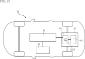
- FIG. 13 is a schematic diagram of a vehicle on which the semiconductor device shown in FIG. 1 is mounted.
- FIG. 14 is a plan view of the semiconductor device according to the second embodiment of the present disclosure, seen through the sealing resin.
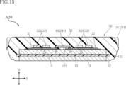
- FIG. 15 is a cross-sectional view taken along line XV-XV in FIG. FIG.
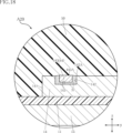
- FIG. 16 is a cross-sectional view taken along line XVI-XVI in FIG.
- FIG. 17 is a partially enlarged view of FIG.
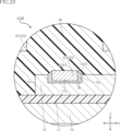
- FIG. 18 is a cross-sectional view taken along line XVIII-XVIII in FIG.
- FIG. 19 is a plan view of the semiconductor device according to the third embodiment of the present disclosure, seen through the sealing resin.
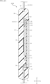
- FIG. 20 is a cross-sectional view taken along line XX-XX in FIG.
- FIG. 21 is a cross-sectional view taken along line XXI-XXI in FIG.
- FIG. 22 is a partially enlarged view of FIG.
- FIG. 23 is a cross-sectional view taken along line XXIII-XXIII in FIG.
- FIG. 24 is a plan view of the semiconductor device according to the fourth embodiment of the present disclosure, seen through the sealing resin.
- FIG. 25 is a cross-sectional view taken along line XXV-XXV in FIG.
- a semiconductor device A10 according to a first embodiment of the present disclosure will be described with reference to FIGS. 1 to 10.
- the semiconductor device A10 is generally used in a power conversion circuit such as an inverter.
- the semiconductor device A10 includes an insulating layer 11, a conductive layer 12, a heat dissipation layer 13, a first wiring layer 14, a first semiconductor element 21, a second semiconductor element 22, a first terminal 31, a second terminal 32, a first signal terminal 33, a second signal terminal 34, a bonding layer 39, and a sealing resin 50.
- the semiconductor device A10 further includes a first conductive member 41, a second conductive member 42, and a third conductive member 43.
- FIG. 2 shows the sealing resin 50 through the insulating layer 11 for ease of understanding.
- the sealing resin 50 through the insulating layer 11 is shown by an imaginary line (double-dashed line).
- first direction z the normal direction of the mounting surface 121 of the conductive layer 12 described below
- second direction x One direction that is orthogonal to the first direction z
- third direction y The direction that is orthogonal to both the first direction z and the second direction x.
- the sealing resin 50 covers the first semiconductor element 21 and the second semiconductor element 22.
- the sealing resin 50 is an insulator.
- the sealing resin 50 is made of a material that contains, for example, black epoxy resin.
- the sealing resin 50 has a top surface 51, a bottom surface 52, a first side surface 53, and a second side surface 54.
- the top surface 51 faces the same side as the mounting surface 121 of the conductive layer 12, which will be described later, in the first direction z.
- the bottom surface 52 faces the opposite side to the top surface 51 in the first direction z.
- first side surface 53 and the second side surface 54 face in opposite directions in the second direction x.
- Each of the first side surface 53 and the second side surface 54 is connected to the top surface 51 and the bottom surface 52.
- the insulating layer 11 is covered with a sealing resin 50.
- the insulating layer 11 is made of a material having a relatively high thermal conductivity.
- the insulating layer 11 is made of a ceramic containing either silicon nitride ( Si3N4 ) or aluminum nitride (AlN).
- the insulating layer 11 may be made of a material containing resin.
- the conductive layer 12 is bonded to one side of the insulating layer 11 in the first direction z.
- the conductive layer 12 carries a first semiconductor element 21 and a second semiconductor element 22.
- the conductive layer 12 is surrounded by the periphery 111 of the insulating layer 11.
- the conductive layer 12 is covered with a sealing resin 50.
- the conductive layer 12 contains copper (Cu).
- the dimension of the conductive layer 12 in the first direction z is larger than the dimension of the insulating layer 11 in the first direction z.
- the conductive layer 12 has a mounting surface 121, an end surface 122, and multiple peripheral surfaces 123.
- the mounting surface 121 faces one side of the first direction z.
- the first semiconductor element 21 and the second semiconductor element 22 face the mounting surface 121.
- the end surface 122 faces a direction perpendicular to the first direction z.
- the end surface 122 is connected to the mounting surface 121.
- Each of the multiple peripheral surfaces 123 faces a direction perpendicular to the first direction z, and is located inside the conductive layer 12 from the end surface 122 when viewed in the first direction z.
- the multiple peripheral surfaces 123 are arranged along the third direction y. As shown in FIG. 10, each of the multiple peripheral surfaces 123 has an upper edge 123A.
- the upper edge 123A corresponds to the boundary between any one of the multiple peripheral surfaces 123 and the mounting surface 121.
- the conductive layer 12 is provided with a plurality of engagement portions 124.
- the plurality of engagement portions 124 are individually defined by a plurality of peripheral surfaces 123.
- each of the plurality of engagement portions 124 is a recess recessed from the mounting surface 121.
- the heat dissipation layer 13 is located on the opposite side of the insulating layer 11 from the conductive layer 12 and is joined to the insulating layer 11.
- the heat dissipation layer 13 is surrounded by the periphery 111 of the insulating layer 11 and overlaps the conductive layer 12.
- the heat dissipation layer 13 is exposed to the outside from the bottom surface 52 of the sealing resin 50.
- the heat dissipation layer 13 contains copper.
- the dimension of the heat dissipation layer 13 in the first direction z is larger than the dimension of the insulating layer 11 in the first direction z and is equal to the dimension of the conductive layer 12 in the first direction z.
- the relationship of the size of the heat dissipation layer 13 in the first direction z to the dimensions of the insulating layer 11 and the conductive layer 12 in the first direction z can be various.
- the first wiring layer 14 is located on the same side as the conductive layer 12 with respect to the insulating layer 11, and is bonded to the insulating layer 11.
- the first wiring layer 14 is located next to the conductive layer 12 in the second direction x.
- the first wiring layer 14 extends in the third direction y.
- the first wiring layer 14 is surrounded by the periphery 111 of the insulating layer 11.
- the first wiring layer 14 is covered with a sealing resin 50.
- the first wiring layer 14 contains copper.
- the dimension of the first wiring layer 14 in the first direction z is larger than the dimension of the insulating layer 11 in the first direction z.
- the first semiconductor element 21 is bonded to the mounting surface 121 of the conductive layer 12, as shown in Figures 5 and 6.
- the first semiconductor element 21 is, for example, a MOSFET (Metal-Oxide-Semiconductor Field-Effect Transistor).
- the first semiconductor element 21 may be a field effect transistor including a MISFET (Metal-Insulator-Semiconductor Field-Effect Transistor) or a bipolar transistor such as an IGBT (Insulated Gate Bipolar Transistor).
- the first semiconductor element 21 is an n-channel type MOSFET with a vertical structure.
- the first semiconductor element 21 includes a compound semiconductor substrate.
- the composition of the compound semiconductor substrate includes silicon carbide (SiC).
- the first semiconductor element 21 has a first electrode 211, two second electrodes 212, and a first gate electrode 213.
- the first electrode 211 is located on one side in the first direction z.
- the first electrode 211 faces the mounting surface 121 of the conductive layer 12.
- the first electrode 211 is conductively bonded to the mounting surface 121 via the conductive bonding layer 29. This allows the first electrode 211 to be electrically connected to the conductive layer 12.
- the conductive bonding layer 29 is, for example, solder.
- the conductive bonding layer 29 may be a sintered metal containing silver or the like.
- a current corresponding to the power before being converted by the first semiconductor element 21 flows through the first electrode 211.
- the first electrode 211 corresponds to the drain of the first semiconductor element 21.
- the two second electrodes 212 are located on the opposite side to the first electrode 211 in the first direction z. As shown in FIG. 2, the two second electrodes 212 are spaced apart from each other in the second direction x. A current corresponding to the power converted by the first semiconductor element 21 flows through each of the two second electrodes 212. In other words, the two second electrodes 212 correspond to the sources of the first semiconductor element 21.
- the first gate electrode 213 is located on the same side as the two second electrodes 212 in the first direction z.
- a gate voltage for driving the first semiconductor element 21 is applied to the first gate electrode 213.
- the first gate electrode 213 is conductive to the first wiring layer 14.
- the area of the first gate electrode 213 is smaller than the area of each of the two second electrodes 212 when viewed in the first direction z.
- the first gate electrode 213 is rectangular when viewed in the first direction z.
- the first gate electrode 213 has a first center C1 when viewed in the first direction z.
- the first center C1 is the intersection of the diagonals of the first gate electrode 213.
- the second semiconductor element 22 is bonded to the mounting surface 121 of the conductive layer 12, as shown in FIG. 5.
- the second semiconductor element 22 is an element of the same type as the first semiconductor element 21. Therefore, the second semiconductor element 22 is an n-channel type MOSFET with a vertical structure.
- the second semiconductor element 22 is located next to the first semiconductor element 21 in the third direction y.
- the second semiconductor element 22 has a third electrode 221, two fourth electrodes 222, and a second gate electrode 223.
- the third electrode 221 is located on one side in the first direction z.
- the third electrode 221 faces the mounting surface 121 of the conductive layer 12.
- the third electrode 221 is conductively bonded to the mounting surface 121 via the conductive bonding layer 29. This allows the third electrode 221 to be electrically connected to the conductive layer 12.
- a current corresponding to the power before being converted by the second semiconductor element 22 flows through the third electrode 221.
- the third electrode 221 corresponds to the drain of the second semiconductor element 22.
- the two fourth electrodes 222 are located on the opposite side to the third electrode 221 in the first direction z. As shown in FIG. 2, the two fourth electrodes 222 are spaced apart from each other in the second direction x. A current corresponding to the power converted by the second semiconductor element 22 flows through each of the two fourth electrodes 222. In other words, the two fourth electrodes 222 correspond to the sources of the second semiconductor element 22.
- the second gate electrode 223 is located on the same side as the two fourth electrodes 222 in the first direction z.
- a gate voltage for driving the second semiconductor element 22 is applied to the second gate electrode 223.
- the second gate electrode 223 is conductive to the first wiring layer 14.
- the area of the second gate electrode 223 is smaller than the area of each of the two fourth electrodes 222 when viewed in the first direction z.
- the second gate electrode 223 is rectangular when viewed in the first direction z.
- the second gate electrode 223 has a second center C2 when viewed in the first direction z.
- the second center C2 is the intersection of the diagonals of the second gate electrode 223.
- the first terminal 31 is located on one side of the first semiconductor element 21 and the second semiconductor element 22 in the second direction x.
- the first terminal 31 is electrically connected to the first electrode 211 of the first semiconductor element 21 and the third electrode 221 of the second semiconductor element 22. Therefore, the first terminal 31 corresponds to the drain terminal of the semiconductor device A10.
- the first terminal 31 contains copper.
- the first terminal 31 has a base 311 and a plurality of joints 312.
- the base 311 is separated from the mounting surface 121 of the conductive layer 12.
- the base 311 includes a portion covered with the sealing resin 50 and a portion exposed to the outside from the first side surface 53 of the sealing resin 50.
- the plurality of joints 312 extend from the base 311 to the side where the first semiconductor element 21 and the second semiconductor element 22 are located in the second direction x.
- the plurality of joints 312 are arranged along the third direction y.
- Each of the plurality of joints 312 is covered with the sealing resin 50.
- the plurality of joints 312 individually overlap the plurality of engagement portions 124 of the conductive layer 12.
- the bonding layer 39 conductively bonds the multiple engagement portions 124 of the conductive layer 12 to the multiple bonding portions 312 of the first terminal 31 individually.
- the first terminal 31 is electrically connected to the first electrode 211 of the first semiconductor element 21 and the third electrode 221 of the second semiconductor element 22.
- the bonding layer 39 is, for example, solder.
- each of the multiple joints 312 of the first terminal 31 is accommodated in one of the multiple engagement portions 124 of the conductive layer 12.
- the joint layer 39 contacts the multiple peripheral surfaces 123 of the conductive layer 12 that define each of the multiple engagement portions 124. Furthermore, the joint layer 39 contacts the upper edge 123A of each of the multiple peripheral surfaces 123.
- each of the multiple joints 312 has an upper surface 312A that faces the same side as the mounting surface 121 of the conductive layer 12 in the first direction z.
- the joint layer 39 contacts the edge of the upper surface 312A.
- the second terminal 32 is conductively joined to the two second electrodes 212 of the first semiconductor element 21 and the two fourth electrodes 222 of the second semiconductor element 22. As a result, the second terminal 32 is electrically connected to each of the two second electrodes 212 and each of the two fourth electrodes 222. Therefore, the second terminal 32 corresponds to the source terminal of the semiconductor device A10.
- the second terminal 32 contains copper.
- the second terminal 32 has a base 321, a plurality of first bonding portions 322, and a plurality of second bonding portions 323.
- the base 321 overlaps the mounting surface 121 of the conductive layer 12.
- the base 321 includes a portion covered with the sealing resin 50 and a portion exposed to the outside from the second side surface 54 of the sealing resin 50.
- Each of the plurality of first bonding portions 322 is connected to the base 321 and covered with the sealing resin 50.
- each of the plurality of first bonding portions 322 protrudes from the base 321 toward the first semiconductor element 21.
- Each of the plurality of first bonding portions 322 is conductively bonded to one of the two second electrodes 212 of the first semiconductor element 21 via the conductive bonding layer 29.
- Each of the plurality of second bonding portions 323 is connected to the base 321 and covered with the sealing resin 50. As shown in FIG. 7, each of the multiple second bonding portions 323 protrudes from the base portion 321 toward the second semiconductor element 22.
- Each of the multiple second bonding portions 323 is conductively bonded to one of the two fourth electrodes 222 of the second semiconductor element 22 via the conductive bonding layer 29.
- the first signal terminal 33 includes a portion covered by the sealing resin 50 and a portion exposed to the outside from the second side surface 54 of the sealing resin 50.
- the first signal terminal 33 is located on one side of the base 321 of the second terminal 32 in the third direction y.
- the first signal terminal 33 is electrically connected to the first wiring layer 14. Therefore, the first signal terminal 33 is electrically connected to the first gate electrode 213 of the first semiconductor element 21 and the second gate electrode 223 of the second semiconductor element 22. In other words, the first signal terminal 33 corresponds to the gate terminal of the semiconductor device A10.
- the first signal terminal 33 includes copper.
- the portion of the first signal terminal 33 exposed to the outside from the second side surface 54 includes a portion extending along the first direction z.
- the second signal terminal 34 includes a portion covered by the sealing resin 50 and a portion exposed to the outside from the second side surface 54 of the sealing resin 50.
- the second signal terminal 34 is located between the first signal terminal 33 and the base 321 of the second terminal 32 in the third direction y. In the semiconductor device A10, the second signal terminal 34 is connected to the base 321. Therefore, the second signal terminal 34 is electrically connected to each of the two second electrodes 212 and each of the two fourth electrodes 222. A voltage having the same potential as the voltage applied to each of the two second electrodes 212 and each of the two fourth electrodes 222 is applied to the second signal terminal 34.
- the second signal terminal 34 includes copper.
- the portion of the second signal terminal 34 exposed to the outside from the second side surface 54 includes a portion extending along the first direction z.
- the first conductive member 41 is conductively bonded to the first gate electrode 213 of the first semiconductor element 21 and the first wiring layer 14. This allows the first wiring layer 14 to be electrically connected to the first gate electrode 213.
- the first conductive member 41 is covered with a sealing resin 50.
- the first conductive member 41 is, for example, a wire containing either aluminum (Al) or gold (Au).
- the second conductive member 42 is conductively bonded to the second gate electrode 223 of the second semiconductor element 22 and the first wiring layer 14. This allows the first wiring layer 14 to be electrically connected to the second gate electrode 223.
- the second conductive member 42 is covered with a sealing resin 50.
- the second conductive member 42 is, for example, a wire containing either aluminum or gold.
- the length of the second conductive member 42 is equal to the length of the first conductive member 41.
- the third conductive member 43 is conductively bonded to the first wiring layer 14 and the first signal terminal 33. This allows the first wiring layer 14 to be electrically connected to the first signal terminal 33.
- the third conductive member 43 is covered with a sealing resin 50.
- the third conductive member 43 is, for example, a wire containing either aluminum or gold. In the semiconductor device A10, the third conductive member 43 is connected to the second conductive member 42.
- the first signal terminal 33 when viewed in the first direction z, has a first contact Ca.
- the third conductive member 43 is conductively joined to the first contact Ca.
- the position of the first contact Ca is not particularly limited as long as it is a portion of the first signal terminal 33 that is covered with the sealing resin 50.
- the first straight line length L1 is the shortest distance connecting the first center C1 located at the first gate electrode 213 of the first semiconductor element 21 and the first contact Ca located at the first signal terminal 33.
- the second straight line length L2 is the shortest distance connecting the second center C2 located at the second gate electrode 223 of the second semiconductor element 22 and the first contact Ca.
- the first conductive path length R1 is the shortest distance of the conductive path from the first center C1 to the first contact Ca via the first conductive member 41, the first wiring layer 14, and the third conductive member 43.
- the second conductive path length R2 is the shortest distance of the conductive path from the second center C2 to the first contact Ca via the second conductive member 42, the first wiring layer 14, and the third conductive member 43.
- the second conductive path length R2/first conductive path length R1 is closer to 1 than the second straight line length L2/first straight line length L1. In other words, when expressed using absolute value symbols (
- FIG. 11 which is a first modified example of the semiconductor device A10, will be described with reference to FIG. 11.
- the cross-sectional position of FIG. 11 is the same as that of FIG. 10.
- each of the multiple engagement portions 124 is a slit that penetrates the conductive layer 12 in the first direction z.
- the bonding layer 39 is in contact with the upper edge 123A of each of the multiple peripheral surfaces 123. Furthermore, the bonding layer 39 is in contact with the edge of the upper surface 312A of each of the multiple joints 312.
- the bonding layer 39 is, for example, solder.
- FIG. 12 The cross-sectional position of FIG. 12 is the same as that of FIG. 10.
- the multiple joints 312 of the first terminal 31 are individually conductively joined to the multiple engagement portions 124 of the conductive layer 12 by welding using a laser or the like.
- a portion of the conductive layer 12 that defines the engagement portion 124 and a portion of the joint 312 in contact therewith are replaced with solidified molten metal formed by welding.
- the solidified molten metal corresponds to the joining layer 39.
- the vehicle B is, for example, an electric vehicle (EV).
- EV electric vehicle
- vehicle B is equipped with an on-board charger 81, a storage battery 82, and a drive system 83.
- Power is supplied to the on-board charger 81 wirelessly from a power supply facility (not shown) installed outdoors. Alternatively, power may be supplied from the power supply facility to the on-board charger 81 via a wired connection.
- the on-board charger 81 is configured with a step-up DC-DC converter. The voltage of the power supplied to the on-board charger 81 is stepped up by the converter and then supplied to the storage battery 82. The stepped-up voltage is, for example, 600V.
- the drive system 83 drives the vehicle B.
- the drive system 83 has an inverter 831 and a drive source 832.
- the semiconductor device A10 constitutes part of the inverter 831.
- the power stored in the storage battery 82 is supplied to the inverter 831.
- the power supplied from the storage battery 82 to the inverter 831 is DC power.
- a step-up DC-DC converter may be further provided between the storage battery 82 and the inverter 831.
- the inverter 831 converts DC power into AC power.
- the inverter 831 including the semiconductor device A10 is conducted to the drive source 832.
- the drive source 832 has an AC motor and a transmission.
- the AC motor rotates and the rotation is transmitted to the transmission.
- the transmission rotates the drive shaft of the vehicle B after appropriately reducing the rotation speed transmitted from the AC motor. This drives vehicle B.
- semiconductor device A10 in inverter 831 is necessary to output AC power with an appropriate frequency change to correspond to the required rotation speed of the AC motor.
- the semiconductor device A10 includes a conductive layer 12, a first semiconductor element 21, a second semiconductor element 22, and a first signal terminal 33.
- the first semiconductor element 21 has a first gate electrode 213.
- the second semiconductor element 22 has a second gate electrode 223.
- a first straight line length L1 connecting the first center C1 of the first gate electrode 213 and the first contact Ca of the first signal terminal 33, and a second straight line length L2 connecting the second center C2 of the second gate electrode 223 and the first contact Ca are defined.
- a first conductive path length R1 from the first center C1 to the first contact Ca, and a second conductive path length R2 from the second center C2 to the first contact Ca are defined.
- the second conductive path length R2/first conductive path length R1 is closer to 1 than the second straight line length L2/first straight line length L1 (see FIG. 2).
- the second conductive path length R2 is approximately equal to the first conductive path length R1. This suppresses resonance caused by the interaction between the current flowing through the conductive path of the first conductive path length R1 and the current flowing through the conductive path of the second conductive path length R2. Therefore, with this configuration, in the semiconductor device A10, it is possible to suppress the resonance phenomenon that occurs when multiple semiconductor elements are operated in parallel.
- the semiconductor device A10 further includes a first terminal 31 electrically connected to the first semiconductor element 21, and a bonding layer 39 that conductively bonds the conductive layer 12 and the first terminal 31.
- the conductive layer 12 is provided with an engagement portion 124 defined by the peripheral surface 123.
- the first terminal 31 has a bonding portion 312 that is conductively bonded to the engagement portion 124.
- the bonding layer 39 conductively bonds the engagement portion 124 and the bonding portion 312.
- the bonding layer 39 is in contact with the peripheral surface 123. When viewed in the first direction z, the bonding portion 312 overlaps the engagement portion 124.
- the bonding layer 39 be in contact with the upper edge 123A of the peripheral surface 123 of the conductive layer 12. This is because the surface tension generated in the molten bonding layer 39 is further increased.
- the bonding portion 312 of the first terminal 31 is housed in the engagement portion 124.
- a larger reaction force is received from the peripheral surface 123 of the conductive layer 12 via the molten bonding layer 39, and the peripheral surface 123 restricts the positional deviation of the bonding portion 312. This effectively prevents the first terminal 31 from being displaced relative to the conductive layer 12, and also prevents the first terminal 31 from rotating around the first direction z.
- the bonding portion 312 of the first terminal 31 has an upper surface 312A that faces the same side as the mounting surface 121 of the conductive layer 12 in the first direction z.
- the bonding layer 39 is in contact with the edge of the upper surface 312A. With this configuration, the surface tension generated in the molten bonding layer 39 is further increased, so that the self-alignment effect described above is more effectively manifested.
- the semiconductor device A10 further includes an insulating layer 11 to which a conductive layer 12 is bonded, and a heat dissipation layer 13 located on the opposite side of the insulating layer 11 from the conductive layer 12 and bonded to the insulating layer 11.
- the insulating layer 11 and the conductive layer 12 are covered with a sealing resin 50.
- the heat dissipation layer 13 is exposed to the outside from the sealing resin 50.
- the conductive layer 12 and the heat dissipation layer 13 are each spaced apart from the periphery 111 of the insulating layer 11.
- the vicinity of the periphery 111 of the insulating layer 11 is sandwiched between the sealing resin 50 on both sides in the first direction z. This makes it possible to prevent the insulating layer 11 and the conductive layer 12 from falling off from the sealing resin 50.
- each of the conductive layer 12 and the heat dissipation layer 13 in the first direction z is greater than the dimension of the insulating layer 11 in the first direction z. This configuration reduces the thermal resistance of each of the conductive layer 12 and the heat dissipation layer 13 in the first direction z. This can further improve the heat dissipation properties of the semiconductor device A10.
- FIG. 14 is seen through the sealing resin 50.
- the see-through sealing resin 50 is shown by imaginary lines.
- Semiconductor device A20 differs from semiconductor device A10 in that it includes a conductive member 44 instead of the first conductive member 41 and the second conductive member 42, that it further includes a first bonding layer 37, and that the configuration of the first wiring layer 14 is different.
- the first wiring layer 14 has a first end surface 141 and a first peripheral surface 142.
- the first end surface 141 faces in a direction perpendicular to the first direction z.
- the first peripheral surface 142 faces in a direction perpendicular to the first direction z and is located inward of the first wiring layer 14 from the first end surface 141 when viewed in the first direction z.
- the first peripheral surface 142 has a first upper edge 142A.
- the first upper edge 142A corresponds to the boundary between the first peripheral surface 142 and the surface of the first wiring layer 14 that faces the same side as the mounting surface 121 of the conductive layer 12 in the first direction z.
- the first wiring layer 14 is provided with a first engagement portion 143.
- the first engagement portion 143 is defined by a first circumferential surface 142.
- the first engagement portion 143 is a recess that is recessed in the first direction z.
- the conductive member 44 is conductively joined to the first gate electrode 213 of the first semiconductor element 21, the second gate electrode 223 of the second semiconductor element 22, and the first engagement portion 143 of the first wiring layer 14.
- the conductive member 44 is a metal lead that contains copper.
- the conductive member 44 is covered with a sealing resin 50.
- the conductive member 44 has a base 441, a first connection portion 442, and a second connection portion 443.
- the base 441 extends in the second direction x.
- the first connection portion 442 is connected to one side of the base 441 in the second direction x.
- the first connection portion 442 extends in the third direction y. As shown in FIG. 15, one side of the first connection portion 442 in the third direction y is conductively bonded to the first gate electrode 213 via the conductive bonding layer 29.
- the other side of the first connection portion 442 in the third direction y is conductively bonded to the second gate electrode 223 via the conductive bonding layer 29.
- the second connection portion 443 is located on the opposite side of the first connection portion 442 with respect to the base 441, and is connected to the base 441. As shown in FIG. 16, at least a part of the second connection portion 443 is accommodated in the first engagement portion 143 of the first wiring layer 14.
- the first bonding layer 37 conductively bonds the first engagement portion 143 of the first wiring layer 14 and the second connection portion 443 of the conductive member 44.
- the first gate electrode 213 of the first semiconductor element 21 and the second gate electrode 223 of the second semiconductor element 22 are each electrically connected to the first wiring layer 14.
- the first bonding layer 37 is, for example, solder.
- the first bonding layer 37 is in contact with the first peripheral surface 142 of the first wiring layer 14, which defines the first engagement portion 143 of the first wiring layer 14. Furthermore, the first bonding layer 37 is in contact with the first upper edge 142A of the first peripheral surface 142. As shown in FIGS. 17 and 18, the second connection portion 443 of the conductive member 44 has an upper surface 443A that faces the same side as the mounting surface 121 of the conductive layer 12 in the first direction z. The first bonding layer 37 is in contact with the edge of the upper surface 443A.
- the semiconductor device A20 includes a conductive layer 12, a first semiconductor element 21, a second semiconductor element 22, and a first signal terminal 33.
- the first semiconductor element 21 has a first gate electrode 213.
- the second semiconductor element 22 has a second gate electrode 223.
- a first straight line length L1 connecting the first center C1 of the first gate electrode 213 and the first contact Ca of the first signal terminal 33, and a second straight line length L2 connecting the second center C2 of the second gate electrode 223 and the first contact Ca are defined.
- a first conductive path length R1 from the first center C1 to the first contact Ca, and a second conductive path length R2 from the second center C2 to the first contact Ca are defined.
- the semiconductor device A20 the second conductive path length R2/first conductive path length R1 is closer to 1 than the second straight line length L2/first straight line length L1 (see FIG. 14). Therefore, with this configuration, the semiconductor device A20 can also suppress the resonance phenomenon that occurs when multiple semiconductor elements are operated in parallel. Furthermore, the semiconductor device A20 has a configuration in common with the semiconductor device A10, and thus achieves the same effects as the semiconductor device A10.
- the semiconductor device A20 includes a conductive member 44 instead of the first conductive member 41 and the second conductive member 42, and further includes a first bonding layer 37 that conductively bonds the first wiring layer 14 and the conductive member 44.
- the first wiring layer 14 is provided with a first engagement portion 143 defined by a first circumferential surface 142.
- the conductive member 44 has a second connection portion 443 that is conductively bonded to the first engagement portion 143 via the first bonding layer 37.
- the first bonding layer 37 is in contact with the first circumferential surface 142. At least a portion of the second connection portion 443 is accommodated in the first engagement portion 143.
- FIG. 19 is seen through the sealing resin 50 for ease of understanding.
- the see-through sealing resin 50 is shown by imaginary lines.
- the semiconductor device A30 differs from the semiconductor device A10 in that it further includes a second wiring layer 15 and a second bonding layer 38, and in the configuration of the second terminal 32 and the second signal terminal 34.
- the second wiring layer 15 is located on the same side as the conductive layer 12 with respect to the insulating layer 11 as a reference, and is bonded to the insulating layer 11.
- the second wiring layer 15 is located on the opposite side to the conductive layer 12 with respect to the first wiring layer 14 as a reference in the second direction x.
- the second wiring layer 15 extends in the third direction y.
- the second wiring layer 15 is surrounded by the periphery 111 of the insulating layer 11.
- the second wiring layer 15 is covered with a sealing resin 50.
- the second wiring layer 15 contains copper.
- the dimension of the second wiring layer 15 in the first direction z is larger than the dimension of the insulating layer 11 in the first direction z.
- the second wiring layer 15 has a second end surface 151 and a second peripheral surface 152.
- the second end surface 151 faces in a direction perpendicular to the first direction z.
- the second peripheral surface 152 faces in a direction perpendicular to the first direction z and is located inside the second wiring layer 15 from the second end surface 151 when viewed in the first direction z.
- the second peripheral surface 152 has a second upper edge 152A.
- the second upper edge 152A corresponds to the boundary between the second peripheral surface 152 and the surface of the second wiring layer 15 that faces the same side as the mounting surface 121 of the conductive layer 12 in the first direction z.
- the second wiring layer 15 is provided with a second engagement portion 153.
- the second engagement portion 153 is defined by a second circumferential surface 152.
- the second engagement portion 153 is a recess that is recessed in the first direction z.
- the second terminal 32 has a support portion 324.
- the support portion 324 is connected to the base portion 321 of the second terminal 32.
- the support portion 324 is covered with the sealing resin 50.
- the support portion 324 is located between the multiple first joint portions 322 of the second terminal 32 and the multiple second joint portions 323 of the second terminal 32.
- at least a portion of the support portion 324 is accommodated in the second engagement portion 153 of the second wiring layer 15.
- the second bonding layer 38 conductively bonds the second engagement portion 153 of the second wiring layer 15 to the support portion 324 of the second terminal 32.
- the second terminal 32, each of the two second electrodes 212 of the first semiconductor element 21, and each of the two fourth electrodes 222 of the second semiconductor element 22 are electrically connected to the second wiring layer 15.
- the second bonding layer 38 contacts the second peripheral surface 152 of the second wiring layer 15, which defines the second engagement portion 153 of the second wiring layer 15. Furthermore, the second bonding layer 38 contacts the second upper edge 152A of the second peripheral surface 152. As shown in FIGS. 22 and 23, the support portion 324 of the second terminal 32 has an upper surface 324A that faces the same side as the mounting surface 121 of the conductive layer 12 in the first direction z. The second bonding layer 38 contacts the edge of the upper surface 324A.
- the second signal terminal 34 is separated from the second terminal 32. As shown in FIG. 21, the second signal terminal 34 is conductively bonded to the second wiring layer 15 via the conductive bonding layer 29. This allows the second signal terminal 34 to be electrically connected to the second wiring layer 15.
- the second signal terminal 34 when viewed in the first direction z, has a second contact Cb.
- the second contact Cb overlaps the second wiring layer 15.
- the position of the second contact Cb is not particularly limited as long as it is a portion of the second signal terminal 34 that is covered with the sealing resin 50.
- each of the two second electrodes 212 of the first semiconductor element 21 is rectangular. Furthermore, when viewed in the first direction z, of the two second electrodes 212, the second electrode 212 closest to the second signal terminal 34 has a third center C3.
- the third center C3 is the intersection of the diagonals of the second electrodes 212.
- each of the two fourth electrodes 222 of the second semiconductor element 22 is rectangular. Furthermore, when viewed in the first direction z, of the two fourth electrodes 222, the fourth electrode 222 closest to the second signal terminal 34 has a fourth center C4.
- the fourth center C4 is the intersection of the diagonals of the fourth electrode 222.
- the third straight line length L3, the fourth straight line length L4, the third conductive path length R3, and the fourth conductive path length R4 are defined.
- the third straight line length L3 is the shortest distance connecting the third center C3 located on one of the two second electrodes 212 of the first semiconductor element 21 and the second contact Cb located on the second signal terminal 34.
- the fourth straight line length L4 is the shortest distance connecting the fourth center C4 located on one of the two fourth electrodes 222 of the second semiconductor element 22 and the second contact Cb.
- the third conductive path length R3 is the shortest distance of the conductive path from the third center C3 to the second contact Cb via the second terminal 32 and the second wiring layer 15.
- the fourth conductive path length R4 is the shortest distance of the conductive path from the fourth center C4 to the second contact Cb via the second terminal 32 and the second wiring layer 15.
- the third conductive path length R3/fourth conductive path length R4 is closer to 1 than the third straight line length L3/fourth straight line length L4.
- the semiconductor device A30 includes a conductive layer 12, a first semiconductor element 21, a second semiconductor element 22, and a first signal terminal 33.
- the first semiconductor element 21 has a first gate electrode 213.
- the second semiconductor element 22 has a second gate electrode 223.
- a first straight line length L1 connecting the first center C1 of the first gate electrode 213 and the first contact Ca of the first signal terminal 33, and a second straight line length L2 connecting the second center C2 of the second gate electrode 223 and the first contact Ca are defined.
- a first conductive path length R1 from the first center C1 to the first contact Ca, and a second conductive path length R2 from the second center C2 to the first contact Ca are defined.
- the semiconductor device A30 the second conductive path length R2/first conductive path length R1 is closer to 1 than the second straight line length L2/first straight line length L1 (see FIG. 19). Therefore, with this configuration, the semiconductor device A30 can also suppress the resonance phenomenon that occurs when multiple semiconductor elements are operated in parallel. Furthermore, the semiconductor device A30 has a configuration in common with the semiconductor device A10, and thus achieves the same effects as the semiconductor device A10.
- the semiconductor device A30 further includes a second signal terminal 34.
- the first semiconductor element 21 has a first electrode 211 conductively bonded to the conductive layer 12 and a second electrode 212 conductive to the second signal terminal 34.
- the second semiconductor element 22 has a third electrode 221 conductively bonded to the conductive layer 12 and a fourth electrode 222 conductive to the second signal terminal 34.
- a third straight line length L3 connecting the third center C3 of the second electrode 212 and the second contact Cb of the second signal terminal 34, and a fourth straight line length L4 connecting the fourth center C4 of the fourth electrode 222 and the second contact Cb are defined.
- a third conductive path length R3 from the third center C3 to the second contact Cb, and a fourth conductive path length R4 from the fourth center C4 to the second contact Cb are defined.
- the fourth conductive path length R4/third conductive path length R3 is closer to 1 than the fourth straight line length L4/third straight line length L3 (see FIG. 19).
- the fourth conductive path length R4 is approximately equal to the third conductive path length R3. This suppresses resonance caused by the interaction between the current flowing through the conductive path of the third conductive path length R3 and the current flowing through the conductive path of the fourth conductive path length R4. Therefore, with this configuration, the semiconductor device A30 can also suppress the resonance phenomenon that occurs when multiple semiconductor elements are operated in parallel.
- the semiconductor device A30 further includes a second wiring layer 15 and a second bonding layer 38 that conductively bonds the second wiring layer 15 and the second terminal 32.
- the second wiring layer 15 is provided with a second engagement portion 153 defined by the second peripheral surface 152.
- the second terminal 32 has a support portion 324 that is conductively bonded to the second engagement portion 153 via the second bonding layer 38.
- the second bonding layer 38 is in contact with the second peripheral surface 152. At least a portion of the support portion 324 is accommodated in the second peripheral surface 152.
- the support portion 324 of the second terminal 32 is connected to the base portion 321 of the second terminal 32. In a direction perpendicular to the first direction z, the support portion 324 is located between the first joint portion 322 and the second joint portion 323 of the second terminal 32.
- FIG. 24 is seen through the sealing resin 50 for ease of understanding.
- the see-through sealing resin 50 is shown by imaginary lines.
- Semiconductor device A40 differs from semiconductor device A30 in that it includes a conductive member 44 instead of the first conductive member 41 and the second conductive member 42, that it further includes a first bonding layer 37, and in the configuration of the first wiring layer 14.
- the configurations of the conductive member 44, first bonding layer 37, and first wiring layer 14 in semiconductor device A40 are similar to those in semiconductor device A20. Therefore, individual descriptions of the conductive member 44, first bonding layer 37, and first wiring layer 14 will be omitted.
- the second connection portion 443 of the conductive member 44 and the support portion 324 of the second terminal 32 each overlap an imaginary straight line VL extending in the second direction x.
- the semiconductor device A40 includes a conductive layer 12, a first semiconductor element 21, a second semiconductor element 22, and a first signal terminal 33.
- the first semiconductor element 21 has a first gate electrode 213.
- the second semiconductor element 22 has a second gate electrode 223.
- a first straight line length L1 connecting the first center C1 of the first gate electrode 213 and the first contact Ca of the first signal terminal 33, and a second straight line length L2 connecting the second center C2 of the second gate electrode 223 and the first contact Ca are defined.
- a first conductive path length R1 from the first center C1 to the first contact Ca, and a second conductive path length R2 from the second center C2 to the first contact Ca are defined.
- the semiconductor device A40 In the semiconductor device A40, the second conductive path length R2/first conductive path length R1 is closer to 1 than the second straight line length L2/first straight line length L1 (see FIG. 24). Therefore, with this configuration, the semiconductor device A40 can also suppress the resonance phenomenon that occurs when multiple semiconductor elements are operated in parallel. Furthermore, the semiconductor device A40 has a configuration in common with the semiconductor device A10, and thus achieves the same effects as the semiconductor device A10.
- the semiconductor device A40 further includes a second signal terminal 34.
- the first semiconductor element 21 has a first electrode 211 conductively bonded to the conductive layer 12 and a second electrode 212 conductive to the second signal terminal 34.
- the second semiconductor element 22 has a third electrode 221 conductively bonded to the conductive layer 12 and a fourth electrode 222 conductive to the second signal terminal 34.
- a third straight line length L3 connecting the third center C3 of the second electrode 212 and the second contact Cb of the second signal terminal 34, and a fourth straight line length L4 connecting the fourth center C4 of the fourth electrode 222 and the second contact Cb are defined.
- a third conductive path length R3 from the third center C3 to the second contact Cb, and a fourth conductive path length R4 from the fourth center C4 to the second contact Cb are defined.
- the fourth conductive path length R4/third conductive path length R3 is closer to 1 than the fourth straight line length L4/third straight line length L3 (see FIG. 24). Therefore, with this configuration, even in the semiconductor device A40, it is possible to suppress the resonance phenomenon that occurs when multiple semiconductor elements are operated in parallel.
- Appendix 1 a conductive layer having a mounting surface facing a first direction; a first semiconductor element having a first gate electrode located on a side opposite to a side facing the mounting surface in the first direction and bonded to the mounting surface; a second semiconductor element having a second gate electrode located on an opposite side to a side facing the mounting surface in the first direction and bonded to the mounting surface; a first signal terminal electrically connected to each of the first gate electrode and the second gate electrode; When viewed in the first direction, the first gate electrode has a first center, When viewed in the first direction, the second gate electrode has a second center, When viewed in the first direction, the first signal terminal has a first contact, a first straight line length connecting the first center and the first contact point is L1; a second straight line length connecting the second center and the first contact point is L2; a first conductive path length from the first center to the first contact is R1; If a second conductive path length from the second center to the first
- a first wiring layer is further provided, 2.
- Appendix 3. a first conductive member conductively connected to the first gate electrode and the first wiring layer; a second conductive member conductively connected to the second gate electrode and the first wiring layer, 3.
- Appendix 4. 4.
- Appendix 5. a conductive member conductively connected to the first gate electrode, the second gate electrode, and the first wiring layer; 3.
- the semiconductor device further comprising: a bonding layer that conductively bonds the first wiring layer and the conductive member.
- the first wiring layer has an end surface facing a direction perpendicular to the first direction, and a peripheral surface facing a direction perpendicular to the first direction and positioned inward of the first wiring layer relative to the end surface as viewed in the first direction; the first wiring layer is provided with an engagement portion defined by the circumferential surface, the conductive member has a connection portion that is conductively connected to the engagement portion via the bonding layer, The bonding layer is in contact with the peripheral surface, 6.
- the semiconductor device according to claim 5, wherein at least a portion of the connection portion is accommodated in the engagement portion.
- the first semiconductor element has a first electrode and a second electrode positioned opposite to each other in the first direction; the second semiconductor element has a third electrode and a fourth electrode positioned opposite to each other in the first direction; 3.
- each of the first electrode and the third electrode is conductively connected to the mounting surface.
- Appendix 8 A first terminal electrically connected to the conductive layer; 8.
- a second signal terminal electrically connected to each of the second electrode and the fourth electrode;
- the second electrode When viewed in the first direction, the second electrode has a third center, When viewed in the first direction, the fourth electrode has a fourth center,
- the second signal terminal When viewed in the first direction, the second signal terminal has a second contact, a third straight line length connecting the third center and the second contact point is L3; a fourth straight line length connecting the fourth center and the second contact point is L4; a third conductive path length from the third center to the second contact is R3; A fourth conductive path length from the fourth center to the second contact is R4.
- the semiconductor device wherein the second terminal and the second signal terminal are each electrically connected to the second wiring layer.
- Appendix 11 a bonding layer that conductively bonds the second wiring layer and the second terminal, the second terminal has a first bonding portion conductively bonded to the second electrode, a second bonding portion conductively bonded to the fourth electrode, and a support portion conductively bonded to the second wiring layer via the bonding layer, 11.
- the semiconductor device according to claim 10 wherein the support portion is located between the first joint portion and the second joint portion in a direction perpendicular to the first direction.
- the second wiring layer has an end surface facing a direction perpendicular to the first direction, and a peripheral surface facing a direction perpendicular to the first direction and positioned inward of the second wiring layer relative to the end surface as viewed in the first direction;
- the second wiring layer is provided with an engagement portion defined by the circumferential surface, the support portion is conductively joined to the engagement portion via the joining layer, The bonding layer is in contact with the peripheral surface, 12.
- Appendix 13 a sealing resin that covers the first semiconductor element and the second semiconductor element, 13.
- the conductive layer and the first wiring layer are bonded to a side of the insulating layer facing the mounting surface in the first direction, 14.
- Appendix 15. a heat dissipation layer located on the opposite side of the insulating layer from the conductive layer and bonded to the insulating layer; When viewed in the first direction, the heat dissipation layer is spaced apart from a periphery of the insulating layer, the insulating layer and the conductive layer are covered with the sealing resin, 15.
- a conductive layer having a mounting surface facing a first direction; a first semiconductor element having a first electrode and a second electrode positioned opposite to each other in the first direction, the first electrode being conductively joined to the mounting surface; a second semiconductor element having a third electrode and a fourth electrode positioned opposite to each other in the first direction, the third electrode being conductively joined to the mounting surface; a signal terminal electrically connected to each of the second electrode and the fourth electrode;
- the second electrode has a first center
- the fourth electrode has a second center
- the signal terminal When viewed in the first direction, has a contact, a first straight line length connecting the first center and the contact point is L1; a second straight line length connecting the second center and the contact point is L2; a first conductive path length from the first center to the contact point is R1;
- a second conductive path length from the second center to the contact point is R2.
- Appendix 18 A wiring layer; a terminal conductively connected to each of the second electrode, the fourth electrode, and the wiring layer; a bonding layer that conductively bonds the wiring layer and the terminal, the signal terminal is electrically connected to the wiring layer; the terminal has a first bonding portion conductively bonded to the second electrode, a second bonding portion conductively bonded to the fourth electrode, and a support portion conductively bonded to the wiring layer via the bonding layer, 18.
- the wiring layer has an end surface facing a direction perpendicular to the first direction, and a peripheral surface facing a direction perpendicular to the first direction and positioned inward of the wiring layer relative to the end surface as viewed in the first direction, the wiring layer is provided with an engagement portion defined by the circumferential surface, the support portion is conductively joined to the engagement portion via the joining layer, The bonding layer is in contact with the peripheral surface, 19.
Landscapes
- Structures Or Materials For Encapsulating Or Coating Semiconductor Devices Or Solid State Devices (AREA)
- Engineering & Computer Science (AREA)
- Microelectronics & Electronic Packaging (AREA)
- Physics & Mathematics (AREA)
- Geometry (AREA)
Abstract
Description
図1~図10に基づき、本開示の第1実施形態にかかる半導体装置A10について説明する。一般的に半導体装置A10は、インバータなどの電力変換回路に用いられる。半導体装置A10は、絶縁層11、導電層12、放熱層13、第1配線層14、第1半導体素子21、第2半導体素子22、第1端子31、第2端子32、第1信号端子33、第2信号端子34、接合層39および封止樹脂50を備える。さらに半導体装置A10は、第1導通部材41、第2導通部材42および第3導通部材43を備える。ここで、図2は、理解の便宜上、封止樹脂50を透過している。図2では、透過した封止樹脂50を想像線(二点鎖線)で示している。
図14~図18に基づき、本開示の第2実施形態にかかる半導体装置A20について説明する。これらの図において、先述した半導体装置A10と同一または類似の要素には同一の符号を付して、重複する説明を省略する。ここで、図14は、理解の便宜上、封止樹脂50を透過している。図14では、透過した封止樹脂50を想像線で示している。
図19~図23に基づき、本開示の第3実施形態にかかる半導体装置A30について説明する。これらの図において、先述した半導体装置A10と同一または類似の要素には同一の符号を付して、重複する説明を省略する。ここで、図19は、理解の便宜上、封止樹脂50を透過している。図19では、透過した封止樹脂50を想像線で示している。
図24および図25に基づき、本開示の第4実施形態にかかる半導体装置A40について説明する。これらの図において、先述した半導体装置A10と同一または類似の要素には同一の符号を付して、重複する説明を省略する。ここで、図24は、理解の便宜上、封止樹脂50を透過している。図24では、透過した封止樹脂50を想像線で示している。
付記1.
第1方向を向く搭載面を有する導電層と、
前記第1方向において前記搭載面に対向する側とは反対側に位置する第1ゲート電極を有するとともに、前記搭載面に接合された第1半導体素子と、
前記第1方向において前記搭載面に対向する側とは反対側に位置する第2ゲート電極を有するとともに、前記搭載面に接合された第2半導体素子と、
前記第1ゲート電極および前記第2ゲート電極の各々に導通する第1信号端子と、を備え、
前記第1方向に視て、前記第1ゲート電極は、第1中心を有し、
前記第1方向に視て、前記第2ゲート電極は、第2中心を有し、
前記第1方向に視て、前記第1信号端子は、第1接点を有し、
前記第1中心と前記第1接点とを結ぶ第1直線長をL1とし、
前記第2中心と前記第1接点とを結ぶ第2直線長をL2とし、
前記第1中心から前記第1接点に至る第1導電経路長をR1とし、
前記第2中心から前記第1接点に至る第2導電経路長をR2とすると、
L2/L1よりもR2/R1の方が1に近い関係を満たす、半導体装置。
付記2.
第1配線層をさらに備え、
前記第1ゲート電極、前記第2ゲート電極および前記第1信号端子の各々は、前記第1配線層に導通している、付記1に記載の半導体装置。
付記3.
前記第1ゲート電極および前記第1配線層に導電接合された第1導通部材と、
前記第2ゲート電極および前記第1配線層に導電接合された第2導通部材と、をさらに備え、
前記第2導通部材の長さは、前記第1導通部材の長さと等しい、付記2に記載の半導体装置。
付記4.
前記第1導通部材および前記第2導通部材は、ワイヤである、付記3に記載の半導体装置。
付記5.
前記第1ゲート電極、前記第2ゲート電極および前記第1配線層に導電接合された導通部材と、
前記第1配線層と前記導通部材とを導電接合する接合層と、をさらに備える、付記2に記載の半導体装置。
付記6.
前記第1配線層は、前記第1方向に対して直交する方向を向く端面と、前記第1方向に対して直交する方向を向き、かつ前記第1方向に視て前記端面よりも前記第1配線層の内方に位置する周面と、を有し、
前記第1配線層には、前記周面により規定された係合部が設けられており、
前記導通部材は、前記接合層を介して前記係合部に導電接合された接続部を有し、
前記接合層は、前記周面に接しており、
前記接続部の少なくとも一部は、前記係合部に収容されている、付記5に記載の半導体装置。
付記7.
前記第1半導体素子は、前記第1方向において互いに反対側に位置する第1電極および第2電極を有し、
前記第2半導体素子は、前記第1方向において互いに反対側に位置する第3電極および第4電極を有し、
前記第1電極および前記第3電極の各々は、前記搭載面に導電接合されている、付記2に記載の半導体装置。
付記8.
前記導電層に導通する第1端子と、
前記第2電極および前記第4電極の各々に導電接合された第2端子と、をさらに備える、付記7に記載の半導体装置。
付記9.
前記第2電極および前記第4電極の各々に導通する第2信号端子をさらに備え、
前記第1方向に視て、前記第2電極は、第3中心を有し、
前記第1方向に視て、前記第4電極は、第4中心を有し、
前記第1方向に視て、前記第2信号端子は、第2接点を有し、
前記第3中心と前記第2接点とを結ぶ第3直線長をL3とし、
前記第4中心と前記第2接点とを結ぶ第4直線長をL4とし、
前記第3中心から前記第2接点に至る第3導電経路長をR3とし、
前記第4中心から前記第2接点に至る第4導電経路長をR4とすると、
L4/L3よりもR4/R3の方が1に近い関係を満たす、付記8に記載の半導体装置。
付記10.
第2配線層をさらに備え、
前記第2端子および前記第2信号端子の各々は、前記第2配線層に導通している、付記9に記載の半導体装置。
付記11.
前記第2配線層と前記第2端子とを導電接合する接合層をさらに備え、
前記第2端子は、前記第2電極に導電接合された第1接合部と、前記第4電極に導電接合された第2接合部と、前記接合層を介して前記第2配線層に導電接合された支持部と、を有し、
前記第1方向に対して直交する方向において、前記支持部は、前記第1接合部と前記第2接合部との間に位置する、付記10に記載の半導体装置。
付記12.
前記第2配線層は、前記第1方向に対して直交する方向を向く端面と、前記第1方向に対して直交する方向を向き、かつ前記第1方向に視て前記端面よりも前記第2配線層の内方に位置する周面と、を有し、
前記第2配線層には、前記周面により規定された係合部が設けられており、
前記支持部は、前記接合層を介して前記係合部に導電接合されており、
前記接合層は、前記周面に接しており、
前記支持部の少なくとも一部は、前記係合部に収容されている、付記11に記載の半導体装置。
付記13.
前記第1半導体素子および前記第2半導体素子を覆う封止樹脂をさらに備え、
前記第1信号端子は、前記封止樹脂から露出する部分を含む、付記2ないし12のいずれかに記載の半導体装置。
付記14.
絶縁層をさらに備え、
前記導電層および前記第1配線層は、前記絶縁層の前記第1方向において前記搭載面が向く側に接合されており、
前記第1方向に視て、前記導電層および前記第1配線層の各々は、前記絶縁層の周縁から離れている、付記13に記載の半導体装置。
付記15.
前記絶縁層を基準として前記導電層とは反対側に位置し、かつ前記絶縁層に接合された放熱層をさらに備え、
前記第1方向に視て、前記放熱層は、前記絶縁層の周縁から離れており、
前記絶縁層および前記導電層は、前記封止樹脂に覆われており、
前記放熱層は、前記封止樹脂から外部に露出している、付記14に記載の半導体装置。
付記16.
前記導電層および前記放熱層の各々の前記第1方向の寸法は、前記絶縁層の前記第1方向の寸法よりも大きい、付記15に記載の半導体装置。
付記17.
第1方向を向く搭載面を有する導電層と、
前記第1方向において互いに反対側に位置する第1電極および第2電極を有するとともに、前記第1電極が前記搭載面に導電接合された第1半導体素子と、
前記第1方向において互いに反対側に位置する第3電極および第4電極を有するとともに、前記第3電極が前記搭載面に導電接合された第2半導体素子と、
前記第2電極および前記第4電極の各々に導通する信号端子と、を備え、
前記第1方向に視て、前記第2電極は、第1中心を有し、
前記第1方向に視て、前記第4電極は、第2中心を有し、
前記第1方向に視て、前記信号端子は、接点を有し、
前記第1中心と前記接点とを結ぶ第1直線長をL1とし、
前記第2中心と前記接点とを結ぶ第2直線長をL2とし、
前記第1中心から前記接点に至る第1導電経路長をR1とし、
前記第2中心から前記接点に至る第2導電経路長をR2とすると、
L2/L1よりもR2/R1の方が1に近い関係を満たす、半導体装置。
付記18.
配線層と、
前記第2電極、前記第4電極および前記配線層の各々に導電接合された端子と、
前記配線層と前記端子とを導電接合する接合層と、をさらに備え、
前記信号端子は、前記配線層に導通しており、
前記端子は、前記第2電極に導電接合された第1接合部と、前記第4電極に導電接合された第2接合部と、前記接合層を介して前記配線層に導電接合された支持部と、を有し、
前記第1方向に対して直交する方向において、前記支持部は、前記第1接合部と前記第2接合部との間に位置する、付記17に記載の半導体装置。
付記19.
前記配線層は、前記第1方向に対して直交する方向を向く端面と、前記第1方向に対して直交する方向を向き、かつ前記第1方向に視て前記端面よりも前記配線層の内方に位置する周面と、を有し、
前記配線層には、前記周面により規定された係合部が設けられており、
前記支持部は、前記接合層を介して前記係合部に導電接合されており、
前記接合層は、前記周面に接しており、
前記支持部の少なくとも一部は、前記係合部に収容されている、付記18に記載の半導体装置。
付記20.
駆動源と、
付記13に記載の半導体装置と、を備え、
前記半導体装置は、前記駆動源に導通している、車両。
111:周縁 12:導電層
121:搭載面 122:端面
123:周面 123A:上縁
124:係合部 13:放熱層
14:第1配線層 141:第1端面
142:第1周面 142A:第1上縁
143:第1係合部 15:第2配線層
151:第2端面 152:第2周面
152A:第2上縁 153:第2係合部
21:第1半導体素子 211:第1電極
212:第2電極 213:第1ゲート電極
22:第2半導体素子 221:第3電極
222:第4電極 223:第2ゲート電極
29:導電接合層 31:第1端子
311:基部 312:接合部
312A:上面 32:第2端子
321:基部 322:第1接合部
323:第2接合部 324:支持部
324A:上面 33:第1信号端子
34:第2信号端子 37:第1接合層
38:第2接合層 39:接合層
41:第1導通部材 42:第2導通部材
43:第3導通部材 44:導通部材
441:基部 442:第1接続部
443:第2接続部 443A:上面
50:封止樹脂 51:頂面
52:底面 53:第1側面
54:第2側面 81:車載充電器
82:蓄電池 83:駆動系統
831:インバータ 832:駆動源
C1~C4:第1中心~第4中心 Ca:第1接点
Cb:第2接点 L1~L4:第1直線長~第4直線長
R1~R4:第1導電経路長~第4導電経路長 z:第1方向
x:第2方向 y:第3方向
Claims (20)
- 第1方向を向く搭載面を有する導電層と、
前記第1方向において前記搭載面に対向する側とは反対側に位置する第1ゲート電極を有するとともに、前記搭載面に接合された第1半導体素子と、
前記第1方向において前記搭載面に対向する側とは反対側に位置する第2ゲート電極を有するとともに、前記搭載面に接合された第2半導体素子と、
前記第1ゲート電極および前記第2ゲート電極の各々に導通する第1信号端子と、を備え、
前記第1方向に視て、前記第1ゲート電極は、第1中心を有し、
前記第1方向に視て、前記第2ゲート電極は、第2中心を有し、
前記第1方向に視て、前記第1信号端子は、第1接点を有し、
前記第1中心と前記第1接点とを結ぶ第1直線長をL1とし、
前記第2中心と前記第1接点とを結ぶ第2直線長をL2とし、
前記第1中心から前記第1接点に至る第1導電経路長をR1とし、
前記第2中心から前記第1接点に至る第2導電経路長をR2とすると、
L2/L1よりもR2/R1の方が1に近い関係を満たす、半導体装置。 - 第1配線層をさらに備え、
前記第1ゲート電極、前記第2ゲート電極および前記第1信号端子の各々は、前記第1配線層に導通している、請求項1に記載の半導体装置。 - 前記第1ゲート電極および前記第1配線層に導電接合された第1導通部材と、
前記第2ゲート電極および前記第1配線層に導電接合された第2導通部材と、をさらに備え、
前記第2導通部材の長さは、前記第1導通部材の長さと等しい、請求項2に記載の半導体装置。 - 前記第1導通部材および前記第2導通部材は、ワイヤである、請求項3に記載の半導体装置。
- 前記第1ゲート電極、前記第2ゲート電極および前記第1配線層に導電接合された導通部材と、
前記第1配線層と前記導通部材とを導電接合する接合層と、をさらに備える、請求項2に記載の半導体装置。 - 前記第1配線層は、前記第1方向に対して直交する方向を向く端面と、前記第1方向に対して直交する方向を向き、かつ前記第1方向に視て前記端面よりも前記第1配線層の内方に位置する周面と、を有し、
前記第1配線層には、前記周面により規定された係合部が設けられており、
前記導通部材は、前記接合層を介して前記係合部に導電接合された接続部を有し、
前記接合層は、前記周面に接しており、
前記接続部の少なくとも一部は、前記係合部に収容されている、請求項5に記載の半導体装置。 - 前記第1半導体素子は、前記第1方向において互いに反対側に位置する第1電極および第2電極を有し、
前記第2半導体素子は、前記第1方向において互いに反対側に位置する第3電極および第4電極を有し、
前記第1電極および前記第3電極の各々は、前記搭載面に導電接合されている、請求項2に記載の半導体装置。 - 前記導電層に導通する第1端子と、
前記第2電極および前記第4電極の各々に導電接合された第2端子と、をさらに備える、請求項7に記載の半導体装置。 - 前記第2電極および前記第4電極の各々に導通する第2信号端子をさらに備え、
前記第1方向に視て、前記第2電極は、第3中心を有し、
前記第1方向に視て、前記第4電極は、第4中心を有し、
前記第1方向に視て、前記第2信号端子は、第2接点を有し、
前記第3中心と前記第2接点とを結ぶ第3直線長をL3とし、
前記第4中心と前記第2接点とを結ぶ第4直線長をL4とし、
前記第3中心から前記第2接点に至る第3導電経路長をR3とし、
前記第4中心から前記第2接点に至る第4導電経路長をR4とすると、
L4/L3よりもR4/R3の方が1に近い関係を満たす、請求項8に記載の半導体装置。 - 第2配線層をさらに備え、
前記第2端子および前記第2信号端子の各々は、前記第2配線層に導通している、請求項9に記載の半導体装置。 - 前記第2配線層と前記第2端子とを導電接合する接合層をさらに備え、
前記第2端子は、前記第2電極に導電接合された第1接合部と、前記第4電極に導電接合された第2接合部と、前記接合層を介して前記第2配線層に導電接合された支持部と、を有し、
前記第1方向に対して直交する方向において、前記支持部は、前記第1接合部と前記第2接合部との間に位置する、請求項10に記載の半導体装置。 - 前記第2配線層は、前記第1方向に対して直交する方向を向く端面と、前記第1方向に対して直交する方向を向き、かつ前記第1方向に視て前記端面よりも前記第2配線層の内方に位置する周面と、を有し、
前記第2配線層には、前記周面により規定された係合部が設けられており、
前記支持部は、前記接合層を介して前記係合部に導電接合されており、
前記接合層は、前記周面に接しており、
前記支持部の少なくとも一部は、前記係合部に収容されている、請求項11に記載の半導体装置。 - 前記第1半導体素子および前記第2半導体素子を覆う封止樹脂をさらに備え、
前記第1信号端子は、前記封止樹脂から露出する部分を含む、請求項2ないし12のいずれかに記載の半導体装置。 - 絶縁層をさらに備え、
前記導電層および前記第1配線層は、前記絶縁層の前記第1方向において前記搭載面が向く側に接合されており、
前記第1方向に視て、前記導電層および前記第1配線層の各々は、前記絶縁層の周縁から離れている、請求項13に記載の半導体装置。 - 前記絶縁層を基準として前記導電層とは反対側に位置し、かつ前記絶縁層に接合された放熱層をさらに備え、
前記第1方向に視て、前記放熱層は、前記絶縁層の周縁から離れており、
前記絶縁層および前記導電層は、前記封止樹脂に覆われており、
前記放熱層は、前記封止樹脂から外部に露出している、請求項14に記載の半導体装置。 - 前記導電層および前記放熱層の各々の前記第1方向の寸法は、前記絶縁層の前記第1方向の寸法よりも大きい、請求項15に記載の半導体装置。
- 第1方向を向く搭載面を有する導電層と、
前記第1方向において互いに反対側に位置する第1電極および第2電極を有するとともに、前記第1電極が前記搭載面に導電接合された第1半導体素子と、
前記第1方向において互いに反対側に位置する第3電極および第4電極を有するとともに、前記第3電極が前記搭載面に導電接合された第2半導体素子と、
前記第2電極および前記第4電極の各々に導通する信号端子と、を備え、
前記第1方向に視て、前記第2電極は、第1中心を有し、
前記第1方向に視て、前記第4電極は、第2中心を有し、
前記第1方向に視て、前記信号端子は、接点を有し、
前記第1中心と前記接点とを結ぶ第1直線長をL1とし、
前記第2中心と前記接点とを結ぶ第2直線長をL2とし、
前記第1中心から前記接点に至る第1導電経路長をR1とし、
前記第2中心から前記接点に至る第2導電経路長をR2とすると、
L2/L1よりもR2/R1の方が1に近い関係を満たす、半導体装置。 - 配線層と、
前記第2電極、前記第4電極および前記配線層の各々に導電接合された端子と、
前記配線層と前記端子とを導電接合する接合層と、をさらに備え、
前記信号端子は、前記配線層に導通しており、
前記端子は、前記第2電極に導電接合された第1接合部と、前記第4電極に導電接合された第2接合部と、前記接合層を介して前記配線層に導電接合された支持部と、を有し、
前記第1方向に対して直交する方向において、前記支持部は、前記第1接合部と前記第2接合部との間に位置する、請求項17に記載の半導体装置。 - 前記配線層は、前記第1方向に対して直交する方向を向く端面と、前記第1方向に対して直交する方向を向き、かつ前記第1方向に視て前記端面よりも前記配線層の内方に位置する周面と、を有し、
前記配線層には、前記周面により規定された係合部が設けられており、
前記支持部は、前記接合層を介して前記係合部に導電接合されており、
前記接合層は、前記周面に接しており、
前記支持部の少なくとも一部は、前記係合部に収容されている、請求項18に記載の半導体装置。 - 駆動源と、
請求項13に記載の半導体装置と、を備え、
前記半導体装置は、前記駆動源に導通している、車両。
Priority Applications (4)
| Application Number | Priority Date | Filing Date | Title |
|---|---|---|---|
| DE112024000610.8T DE112024000610T5 (de) | 2023-02-20 | 2024-01-30 | Halbleiterbauteil und fahrzeug |
| CN202480012374.7A CN120770212A (zh) | 2023-02-20 | 2024-01-30 | 半导体装置以及车辆 |
| JP2025502209A JPWO2024176751A1 (ja) | 2023-02-20 | 2024-01-30 | |
| US19/298,926 US20250372511A1 (en) | 2023-02-20 | 2025-08-13 | Semiconductor device and vehicle |
Applications Claiming Priority (2)
| Application Number | Priority Date | Filing Date | Title |
|---|---|---|---|
| JP2023-024455 | 2023-02-20 | ||
| JP2023024455 | 2023-02-20 |
Related Child Applications (1)
| Application Number | Title | Priority Date | Filing Date |
|---|---|---|---|
| US19/298,926 Continuation US20250372511A1 (en) | 2023-02-20 | 2025-08-13 | Semiconductor device and vehicle |
Publications (1)
| Publication Number | Publication Date |
|---|---|
| WO2024176751A1 true WO2024176751A1 (ja) | 2024-08-29 |
Family
ID=92500661
Family Applications (1)
| Application Number | Title | Priority Date | Filing Date |
|---|---|---|---|
| PCT/JP2024/002755 Ceased WO2024176751A1 (ja) | 2023-02-20 | 2024-01-30 | 半導体装置および車両 |
Country Status (5)
| Country | Link |
|---|---|
| US (1) | US20250372511A1 (ja) |
| JP (1) | JPWO2024176751A1 (ja) |
| CN (1) | CN120770212A (ja) |
| DE (1) | DE112024000610T5 (ja) |
| WO (1) | WO2024176751A1 (ja) |
Cited By (1)
| Publication number | Priority date | Publication date | Assignee | Title |
|---|---|---|---|---|
| WO2026053967A1 (ja) * | 2024-09-09 | 2026-03-12 | ローム株式会社 | 半導体モジュール |
Citations (6)
| Publication number | Priority date | Publication date | Assignee | Title |
|---|---|---|---|---|
| JP2018133448A (ja) * | 2017-02-15 | 2018-08-23 | 株式会社東芝 | 半導体装置 |
| EP3376538A1 (en) * | 2017-03-15 | 2018-09-19 | Infineon Technologies AG | Semiconductor arrangement with controllable semiconductor elements |
| JP2019140236A (ja) * | 2018-02-09 | 2019-08-22 | トヨタ自動車株式会社 | 半導体装置 |
| JP2021097145A (ja) * | 2019-12-17 | 2021-06-24 | 富士電機株式会社 | 半導体装置 |
| JP2021097146A (ja) * | 2019-12-18 | 2021-06-24 | 富士電機株式会社 | 半導体装置 |
| JP2021141219A (ja) * | 2020-03-06 | 2021-09-16 | 富士電機株式会社 | 半導体モジュール |
-
2024
- 2024-01-30 CN CN202480012374.7A patent/CN120770212A/zh active Pending
- 2024-01-30 WO PCT/JP2024/002755 patent/WO2024176751A1/ja not_active Ceased
- 2024-01-30 JP JP2025502209A patent/JPWO2024176751A1/ja active Pending
- 2024-01-30 DE DE112024000610.8T patent/DE112024000610T5/de active Pending
-
2025
- 2025-08-13 US US19/298,926 patent/US20250372511A1/en active Pending
Patent Citations (6)
| Publication number | Priority date | Publication date | Assignee | Title |
|---|---|---|---|---|
| JP2018133448A (ja) * | 2017-02-15 | 2018-08-23 | 株式会社東芝 | 半導体装置 |
| EP3376538A1 (en) * | 2017-03-15 | 2018-09-19 | Infineon Technologies AG | Semiconductor arrangement with controllable semiconductor elements |
| JP2019140236A (ja) * | 2018-02-09 | 2019-08-22 | トヨタ自動車株式会社 | 半導体装置 |
| JP2021097145A (ja) * | 2019-12-17 | 2021-06-24 | 富士電機株式会社 | 半導体装置 |
| JP2021097146A (ja) * | 2019-12-18 | 2021-06-24 | 富士電機株式会社 | 半導体装置 |
| JP2021141219A (ja) * | 2020-03-06 | 2021-09-16 | 富士電機株式会社 | 半導体モジュール |
Cited By (1)
| Publication number | Priority date | Publication date | Assignee | Title |
|---|---|---|---|---|
| WO2026053967A1 (ja) * | 2024-09-09 | 2026-03-12 | ローム株式会社 | 半導体モジュール |
Also Published As
| Publication number | Publication date |
|---|---|
| CN120770212A (zh) | 2025-10-10 |
| JPWO2024176751A1 (ja) | 2024-08-29 |
| DE112024000610T5 (de) | 2025-11-13 |
| US20250372511A1 (en) | 2025-12-04 |
Similar Documents
| Publication | Publication Date | Title |
|---|---|---|
| US12068235B2 (en) | Semiconductor device | |
| WO2021005916A1 (ja) | 半導体装置及び電子装置 | |
| US20250372511A1 (en) | Semiconductor device and vehicle | |
| US20250374649A1 (en) | Semiconductor device and vehicle | |
| WO2025142335A1 (ja) | 半導体装置 | |
| WO2024247629A1 (ja) | 半導体装置および車両 | |
| WO2023149257A1 (ja) | 半導体装置 | |
| WO2023190180A1 (ja) | 半導体装置 | |
| JP3922698B2 (ja) | 半導体装置 | |
| US20250338597A1 (en) | Semiconductor device and vehicle | |
| US20260096491A1 (en) | Semiconductor device and vehicle | |
| US20260053054A1 (en) | Semiconductor device, method for manufacturing semiconductor device, and vehicle | |
| JP2025098863A (ja) | 半導体装置および車両 | |
| US20240429154A1 (en) | Semiconductor device | |
| WO2024203152A1 (ja) | 半導体モジュール、半導体装置および車両 | |
| WO2024162052A1 (ja) | 半導体装置および車両 | |
| WO2025216041A1 (ja) | 半導体装置およびインバータシステム | |
| WO2025121140A1 (ja) | 半導体装置、半導体装置の製造方法、インバータ装置および車両 | |
| WO2025192191A1 (ja) | 半導体装置、電力変換ユニットおよび車両 | |
| WO2025109999A1 (ja) | 半導体装置、半導体モジュールおよび車両 | |
| WO2023218943A1 (ja) | 半導体装置 | |
| JP2024175866A (ja) | 半導体装置、半導体装置の製造方法、および車両 | |
| WO2025169688A1 (ja) | 半導体装置 | |
| WO2025258458A1 (ja) | 半導体装置および半導体モジュール | |
| WO2024228322A1 (ja) | 半導体装置 |
Legal Events
| Date | Code | Title | Description |
|---|---|---|---|
| 121 | Ep: the epo has been informed by wipo that ep was designated in this application |
Ref document number: 24760058 Country of ref document: EP Kind code of ref document: A1 |
|
| ENP | Entry into the national phase |
Ref document number: 2025502209 Country of ref document: JP Kind code of ref document: A |
|
| WWE | Wipo information: entry into national phase |
Ref document number: 2025502209 Country of ref document: JP |
|
| WWE | Wipo information: entry into national phase |
Ref document number: 202480012374.7 Country of ref document: CN |
|
| WWE | Wipo information: entry into national phase |
Ref document number: 112024000610 Country of ref document: DE |
|
| WWP | Wipo information: published in national office |
Ref document number: 202480012374.7 Country of ref document: CN |
|
| 122 | Ep: pct application non-entry in european phase |
Ref document number: 24760058 Country of ref document: EP Kind code of ref document: A1 |