WO2024176604A1 - 照明装置 - Google Patents
照明装置 Download PDFInfo
- Publication number
- WO2024176604A1 WO2024176604A1 PCT/JP2023/045907 JP2023045907W WO2024176604A1 WO 2024176604 A1 WO2024176604 A1 WO 2024176604A1 JP 2023045907 W JP2023045907 W JP 2023045907W WO 2024176604 A1 WO2024176604 A1 WO 2024176604A1
- Authority
- WO
- WIPO (PCT)
- Prior art keywords
- liquid crystal
- crystal cell
- pulse signal
- potential
- transparent electrode
- Prior art date
- Legal status (The legal status is an assumption and is not a legal conclusion. Google has not performed a legal analysis and makes no representation as to the accuracy of the status listed.)
- Ceased
Links
Images







Classifications
-
- F—MECHANICAL ENGINEERING; LIGHTING; HEATING; WEAPONS; BLASTING
- F21—LIGHTING
- F21V—FUNCTIONAL FEATURES OR DETAILS OF LIGHTING DEVICES OR SYSTEMS THEREOF; STRUCTURAL COMBINATIONS OF LIGHTING DEVICES WITH OTHER ARTICLES, NOT OTHERWISE PROVIDED FOR
- F21V9/00—Elements for modifying spectral properties, polarisation or intensity of the light emitted, e.g. filters
- F21V9/40—Elements for modifying spectral properties, polarisation or intensity of the light emitted, e.g. filters with provision for controlling spectral properties, e.g. colour, or intensity
-
- G—PHYSICS
- G02—OPTICS
- G02F—OPTICAL DEVICES OR ARRANGEMENTS FOR THE CONTROL OF LIGHT BY MODIFICATION OF THE OPTICAL PROPERTIES OF THE MEDIA OF THE ELEMENTS INVOLVED THEREIN; NON-LINEAR OPTICS; FREQUENCY-CHANGING OF LIGHT; OPTICAL LOGIC ELEMENTS; OPTICAL ANALOGUE/DIGITAL CONVERTERS
- G02F1/00—Devices or arrangements for the control of the intensity, colour, phase, polarisation or direction of light arriving from an independent light source, e.g. switching, gating or modulating; Non-linear optics
- G02F1/01—Devices or arrangements for the control of the intensity, colour, phase, polarisation or direction of light arriving from an independent light source, e.g. switching, gating or modulating; Non-linear optics for the control of the intensity, phase, polarisation or colour
- G02F1/13—Devices or arrangements for the control of the intensity, colour, phase, polarisation or direction of light arriving from an independent light source, e.g. switching, gating or modulating; Non-linear optics for the control of the intensity, phase, polarisation or colour based on liquid crystals, e.g. single liquid crystal display cells
-
- G—PHYSICS
- G02—OPTICS
- G02F—OPTICAL DEVICES OR ARRANGEMENTS FOR THE CONTROL OF LIGHT BY MODIFICATION OF THE OPTICAL PROPERTIES OF THE MEDIA OF THE ELEMENTS INVOLVED THEREIN; NON-LINEAR OPTICS; FREQUENCY-CHANGING OF LIGHT; OPTICAL LOGIC ELEMENTS; OPTICAL ANALOGUE/DIGITAL CONVERTERS
- G02F1/00—Devices or arrangements for the control of the intensity, colour, phase, polarisation or direction of light arriving from an independent light source, e.g. switching, gating or modulating; Non-linear optics
- G02F1/01—Devices or arrangements for the control of the intensity, colour, phase, polarisation or direction of light arriving from an independent light source, e.g. switching, gating or modulating; Non-linear optics for the control of the intensity, phase, polarisation or colour
- G02F1/13—Devices or arrangements for the control of the intensity, colour, phase, polarisation or direction of light arriving from an independent light source, e.g. switching, gating or modulating; Non-linear optics for the control of the intensity, phase, polarisation or colour based on liquid crystals, e.g. single liquid crystal display cells
- G02F1/133—Constructional arrangements; Operation of liquid crystal cells; Circuit arrangements
-
- G—PHYSICS
- G02—OPTICS
- G02F—OPTICAL DEVICES OR ARRANGEMENTS FOR THE CONTROL OF LIGHT BY MODIFICATION OF THE OPTICAL PROPERTIES OF THE MEDIA OF THE ELEMENTS INVOLVED THEREIN; NON-LINEAR OPTICS; FREQUENCY-CHANGING OF LIGHT; OPTICAL LOGIC ELEMENTS; OPTICAL ANALOGUE/DIGITAL CONVERTERS
- G02F1/00—Devices or arrangements for the control of the intensity, colour, phase, polarisation or direction of light arriving from an independent light source, e.g. switching, gating or modulating; Non-linear optics
- G02F1/01—Devices or arrangements for the control of the intensity, colour, phase, polarisation or direction of light arriving from an independent light source, e.g. switching, gating or modulating; Non-linear optics for the control of the intensity, phase, polarisation or colour
- G02F1/13—Devices or arrangements for the control of the intensity, colour, phase, polarisation or direction of light arriving from an independent light source, e.g. switching, gating or modulating; Non-linear optics for the control of the intensity, phase, polarisation or colour based on liquid crystals, e.g. single liquid crystal display cells
- G02F1/133—Constructional arrangements; Operation of liquid crystal cells; Circuit arrangements
- G02F1/1333—Constructional arrangements; Manufacturing methods
- G02F1/1337—Surface-induced orientation of the liquid crystal molecules, e.g. by alignment layers
-
- G—PHYSICS
- G02—OPTICS
- G02F—OPTICAL DEVICES OR ARRANGEMENTS FOR THE CONTROL OF LIGHT BY MODIFICATION OF THE OPTICAL PROPERTIES OF THE MEDIA OF THE ELEMENTS INVOLVED THEREIN; NON-LINEAR OPTICS; FREQUENCY-CHANGING OF LIGHT; OPTICAL LOGIC ELEMENTS; OPTICAL ANALOGUE/DIGITAL CONVERTERS
- G02F1/00—Devices or arrangements for the control of the intensity, colour, phase, polarisation or direction of light arriving from an independent light source, e.g. switching, gating or modulating; Non-linear optics
- G02F1/01—Devices or arrangements for the control of the intensity, colour, phase, polarisation or direction of light arriving from an independent light source, e.g. switching, gating or modulating; Non-linear optics for the control of the intensity, phase, polarisation or colour
- G02F1/13—Devices or arrangements for the control of the intensity, colour, phase, polarisation or direction of light arriving from an independent light source, e.g. switching, gating or modulating; Non-linear optics for the control of the intensity, phase, polarisation or colour based on liquid crystals, e.g. single liquid crystal display cells
- G02F1/133—Constructional arrangements; Operation of liquid crystal cells; Circuit arrangements
- G02F1/1333—Constructional arrangements; Manufacturing methods
- G02F1/1343—Electrodes
-
- G—PHYSICS
- G02—OPTICS
- G02F—OPTICAL DEVICES OR ARRANGEMENTS FOR THE CONTROL OF LIGHT BY MODIFICATION OF THE OPTICAL PROPERTIES OF THE MEDIA OF THE ELEMENTS INVOLVED THEREIN; NON-LINEAR OPTICS; FREQUENCY-CHANGING OF LIGHT; OPTICAL LOGIC ELEMENTS; OPTICAL ANALOGUE/DIGITAL CONVERTERS
- G02F1/00—Devices or arrangements for the control of the intensity, colour, phase, polarisation or direction of light arriving from an independent light source, e.g. switching, gating or modulating; Non-linear optics
- G02F1/01—Devices or arrangements for the control of the intensity, colour, phase, polarisation or direction of light arriving from an independent light source, e.g. switching, gating or modulating; Non-linear optics for the control of the intensity, phase, polarisation or colour
- G02F1/13—Devices or arrangements for the control of the intensity, colour, phase, polarisation or direction of light arriving from an independent light source, e.g. switching, gating or modulating; Non-linear optics for the control of the intensity, phase, polarisation or colour based on liquid crystals, e.g. single liquid crystal display cells
- G02F1/133—Constructional arrangements; Operation of liquid crystal cells; Circuit arrangements
- G02F1/1333—Constructional arrangements; Manufacturing methods
- G02F1/1347—Arrangement of liquid crystal layers or cells in which the final condition of one light beam is achieved by the addition of the effects of two or more layers or cells
-
- F—MECHANICAL ENGINEERING; LIGHTING; HEATING; WEAPONS; BLASTING
- F21—LIGHTING
- F21Y—INDEXING SCHEME ASSOCIATED WITH SUBCLASSES F21K, F21L, F21S and F21V, RELATING TO THE FORM OR THE KIND OF THE LIGHT SOURCES OR OF THE COLOUR OF THE LIGHT EMITTED
- F21Y2115/00—Light-generating elements of semiconductor light sources
- F21Y2115/10—Light-emitting diodes [LED]
Definitions
- One embodiment of the present invention relates to a lighting device that uses liquid crystal to control the distribution of light emitted from a light source.
- liquid crystal lenses optical elements that utilize the change in refractive index of liquid crystals by adjusting the voltage applied to the liquid crystal, known as liquid crystal lenses.
- development of lighting devices that use light sources and liquid crystal lenses is underway (see, for example, Patent Document 1).
- the optical elements of the lighting device are equipped with a control circuit and a microcomputer for controlling the light distribution, and the control circuit includes a digital-to-analog conversion circuit (DAC) and an amplifier circuit (AMP), which occupy a large area.
- DAC digital-to-analog conversion circuit
- AMP amplifier circuit
- a voltage signal is generated for each transparent electrode that applies voltage to the liquid crystal, and optical elements with a large number of transparent electrodes require a large number of DACs and AMPs.
- the control circuit becomes larger and the manufacturing costs increase.
- the microcomputer also increases the manufacturing costs of the lighting device. For this reason, there has been a demand for a lighting device with reduced manufacturing costs.
- one embodiment of the present invention aims to provide a lighting device with reduced manufacturing costs.
- An illumination device includes a light source, an optical element including a first liquid crystal cell and a second liquid crystal cell that transmit light emitted from the light source in a diffusible manner, and a control device connected to the optical element and controlling the optical element, each of the first liquid crystal cell and the second liquid crystal cell including a first substrate having first transparent electrodes and second transparent electrodes arranged alternately extending in a first direction, a second substrate having third transparent electrodes and fourth transparent electrodes arranged alternately extending in a second direction intersecting the first direction, and a liquid crystal layer between the first substrate and the second substrate, and the control device includes:
- the liquid crystal display includes a first non-inverting circuit that outputs a first potential, a first inverting circuit that outputs a second potential having an opposite sign to the first potential, a first multiplexer that is connected to the first non-inverting circuit and the first inverting circuit and outputs a first pulse signal in which the first potential and the second potential are alternately repeated, and a
- An illumination device includes a light source, an optical element including a first liquid crystal cell and a second liquid crystal cell that transmit light emitted from the light source in a diffusible manner, and a control device connected to the optical element and controls the optical element, each of the first liquid crystal cell and the second liquid crystal cell including a first substrate on which first transparent electrodes and second transparent electrodes extending in a first direction are alternately provided, a second substrate on which third transparent electrodes and fourth transparent electrodes extending in a second direction intersecting the first direction are alternately provided, and a liquid crystal layer between the first substrate and the second substrate, and the control device includes a first non-inverting circuit that outputs a first potential, and a second non-inverting circuit that outputs a first potential.
- the liquid crystal display includes a first inversion circuit that outputs a second potential with an inverted sign, a first multiplexer that is connected to the first non-inversion circuit and the first inversion circuit and outputs a first pulse signal in which the first potential and the second potential are alternately repeated, an adder circuit that is connected to the first multiplexer and outputs a second pulse signal in which a predetermined potential is added to the first pulse signal, and a first inverter that is connected to the adder circuit and outputs a third pulse signal in which the phase of the second pulse signal is inverted, and the second pulse signal is input to a first transparent electrode of the first liquid crystal cell, and the third pulse signal is input to a second transparent electrode of the first liquid crystal cell.
- 1 is a schematic diagram showing a configuration of an illumination device according to an embodiment of the present invention
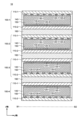
- 1 is a schematic cross-sectional view showing a configuration of an optical element of an illumination device according to one embodiment of the present invention.
- 1 is a schematic cross-sectional view showing a configuration of an optical element of an illumination device according to an embodiment of the present invention.
- 2 is a schematic plan view showing an electrode pattern of a liquid crystal cell included in an optical element of an illumination device according to one embodiment of the present invention.
- FIG. 2 is a schematic plan view showing an electrode pattern of a liquid crystal cell included in an optical element of an illumination device according to one embodiment of the present invention.
- FIG. 1 is a schematic diagram showing a configuration of an illumination device according to an embodiment of the present invention
- 1 is a schematic cross-sectional view showing a configuration of an optical element of an illumination device according to one embodiment of the present invention.
- 2 is a schematic plan view showing an electrode pattern of a liquid crystal cell included in an optical element of an illumination device according to one
- FIG. 1 is a block diagram showing a configuration of a lighting device according to an embodiment of the present invention
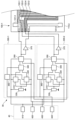
- 2 is a circuit diagram showing a circuit configuration of a control circuit of a lighting device according to an embodiment of the present invention.
- FIG. 2 is a circuit diagram showing a circuit configuration of a control circuit of a lighting device according to an embodiment of the present invention.
- FIG. 1 is a block diagram showing a configuration of a lighting device according to an embodiment of the present invention
- 1 is a block diagram showing a configuration for generating a pulse wave and a fixed potential in a lighting device according to an embodiment of the present invention.
- drawings may show the width, thickness, shape, etc. of each part in a schematic manner compared to the actual embodiment, but these are merely examples, and the illustrated shapes themselves do not limit the interpretation of the present invention.
- elements with similar functions to those explained in relation to previous drawings in the specification may be given the same reference numerals, even if they are in different drawings, and duplicate explanations may be omitted.
- each structure When a film is processed to form multiple structures, each structure may have a different function or role, and each structure may be formed on a different base.
- these multiple structures originate from a film formed as the same layer in the same process, and are made of the same material. Therefore, these multiple films are defined as existing in the same layer.
- the term "above” is used, unless otherwise specified, to include both cases where another structure is placed directly above a structure, in contact with the structure, and cases where another structure is placed above a structure, with yet another structure in between.
- Configuration of lighting device 1] 1 is a schematic diagram showing the configuration of an illumination device 1 according to an embodiment of the present invention. As shown in FIG. 1, the illumination device 1 includes an optical element 10, a light source 20, a control device 30, and a power supply device 40.
- the optical element 10 includes four liquid crystal cells 100 (first liquid crystal cell 100-1, second liquid crystal cell 100-2, third liquid crystal cell 100-3, and fourth liquid crystal cell 100-4).
- the first liquid crystal cell 100-1, second liquid crystal cell 100-2, third liquid crystal cell 100-3, and fourth liquid crystal cell 100-4 are stacked in the z-axis direction in order from the side closest to the light source 20.
- the number of liquid crystal cells 100 included in the optical element 10 is not limited to four. It is sufficient that the optical element 10 includes at least two liquid crystal cells 100. The configuration of the optical element 10 will be described in detail below.
- the light source 20 can emit light to the optical element 10.
- the light emitted from the light source 20 is incident on the first liquid crystal cell 100-1 and is emitted from the fourth liquid crystal cell 100-4.
- the diffusion and polarization of light are controlled by the four liquid crystal cells 100 included in the optical element 10, and the light distribution of the light emitted from the fourth liquid crystal cell 100-4 can be changed.
- the optical element 10 can transmit the light emitted from the light source 20 in a diffusible manner and control the light distribution.
- LEDs light-emitting diodes
- the light source 20 may be any element or device that can emit light.
- the control device 30 is connected to the optical element 10 and can control the optical element 10.
- the control device 30 is provided with eight volume knobs 31 that can be rotated by the user. By changing the combination of rotation of the eight volume knobs 31 and the rotation angle of each of the eight volume knobs 31, the shape or angle of light distribution of the light emitted from the optical element 10 can be adjusted.
- the liquid crystal cell 100 can be controlled by the volume knobs 31.
- two volume knobs 31 are assigned to control one liquid crystal cell 100.
- the volume knobs 31 may be of a sliding type instead of a rotating type. The configuration of the control device 30 will be described in detail later.
- the power supply device 40 is connected to the control device 30 and can supply power to the control device 30. That is, the power supply device 40 can generate a predetermined power supply potential.
- the power supply device 40 can also generate a plurality of power supply potentials (e.g., -7.5V and +7.5V), but is not limited to this.
- the power supply device 40 may also include a power supply potential that is GND (e.g., 0V). For the sake of convenience, this specification may also refer to the case of GND as a power supply potential being generated.
- FIG. 1 illustrates a configuration in which the control device 30 and the power supply device 40 are separate
- the lighting device 1 may also have a configuration in which the control device 30 and the power supply device 40 are integrated.
- FIG. 2A and 2B are schematic cross-sectional views showing a configuration of an optical element 10 of an illumination device 1 according to an embodiment of the present invention. Specifically, Fig. 2A is a cross-sectional view of the optical element 10 taken along line A1-A2 in Fig. 1, and Fig. 2B is a cross-sectional view of the optical element 10 taken along line B1-B2 in Fig. 1.
- each of the first liquid crystal cell 100-1 to the fourth liquid crystal cell 100-4 includes a first substrate 110-1, a second substrate 110-2, a plurality of first transparent electrodes 120-1, a plurality of second transparent electrodes 120-2, a plurality of third transparent electrodes 120-3, a plurality of fourth transparent electrodes 120-4, a first alignment film 130-1, a second alignment film 130-2, a sealant 140, and a liquid crystal layer 150.
- the first transparent electrodes 120-1 and the second transparent electrodes 120-2 are alternately provided on the first substrate 110-1.
- a first alignment film 130-1 is provided on the first substrate 110-1 so as to cover the first transparent electrodes 120-1 and the second transparent electrodes 120-2.
- a third transparent electrode 120-3 and a fourth transparent electrode 120-4 are alternately provided on the second substrate 110-2.
- a second alignment film 130-2 is provided so as to cover the third transparent electrode 120-3 and the fourth transparent electrode 120-4.
- the first substrate 110-1 and the second substrate 110-2 are disposed so that the first transparent electrode 120-1 and the second transparent electrode 120-2 face the third transparent electrode 120-3 and the fourth transparent electrode 120-4, and are bonded via a sealant 140 provided on the periphery of the first substrate 110-1 and the second substrate 110-2.
- a liquid crystal is sealed in the space surrounded by the first substrate 110-1 (more specifically, the first alignment film 130-1), the second substrate 110-2 (more specifically, the second alignment film 130-2), and the sealant 140, and a liquid crystal layer 150 is provided between the first substrate 110-1 and the second substrate 110-2.
- An optically elastic resin layer 160 is provided between the first liquid crystal cell 100-1 and the second liquid crystal cell 100-2. Similarly, an optically elastic resin layer 160 is provided between the second liquid crystal cell 100-2 and the third liquid crystal cell 100-3, and between the third liquid crystal cell 100-3 and the fourth liquid crystal cell 100-4.
- an adhesive containing a light-transmitting acrylic resin can be used as the optically elastic resin layer 160. In other words, the optically elastic resin layer 160 can bond and fix two adjacent liquid crystal cells 100 together.
- Each of the first substrate 110-1 and the second substrate 110-2 may be a rigid substrate having optical transparency, such as a glass substrate, a quartz substrate, or a sapphire substrate. Also, each of the first substrate 110-1 and the second substrate 110-2 may be a flexible substrate having optical transparency, such as a polyimide resin substrate, an acrylic resin substrate, a siloxane resin substrate, or a fluororesin substrate.
- Each of the first transparent electrode 120-1, the second transparent electrode 120-2, the third transparent electrode 120-3, and the fourth transparent electrode 120-4 functions as an electrode for forming an electric field in the liquid crystal layer 150.
- Each of the first transparent electrode 120-1, the second transparent electrode 120-2, the third transparent electrode 120-3, and the fourth transparent electrode 120-4 is made of a transparent conductive material such as indium tin oxide (ITO) or indium zinc oxide (IZO).
- the first transparent electrode 120-1 and the second transparent electrode 120-2 extend in the x-axis direction
- the third transparent electrode 120-3 and the fourth transparent electrode 120-4 extend in the y-axis direction
- the first transparent electrode 120-1 and the second transparent electrode 120-2 extend in the y-axis direction
- the third transparent electrode 120-3 and the fourth transparent electrode 120-4 extend in the x-axis direction.
- first transparent electrode 120-1 to the fourth transparent electrode 120-4 may be described as transparent electrodes 120.
- the first alignment film 130-1 and the second alignment film 130-2 each align the liquid crystal molecules in the liquid crystal layer 150 in a predetermined direction.
- a polyimide resin or the like is used as each of the first alignment film 130-1 and the second alignment film 130-2.
- each of the first alignment film 130-1 and the second alignment film 130-2 may be given alignment characteristics by an alignment treatment such as a rubbing method or a photo-alignment method.
- the rubbing method is a method in which the surface of the alignment film is rubbed in one direction.
- the photo-alignment method is a method in which the alignment film is irradiated with linearly polarized ultraviolet light.
- the first alignment film 130-1 is subjected to an alignment treatment so that the liquid crystal molecules on the first substrate 110-1 side of the liquid crystal layer 150 are aligned in a direction perpendicular to the extension direction of the first transparent electrode 120-1 and the second transparent electrode 120-2.
- the second alignment film 130-2 is subjected to an alignment treatment so that the liquid crystal molecules on the second substrate 110-2 side of the liquid crystal layer 150 are aligned in a direction perpendicular to the extension direction of the third transparent electrode 120-3 and the fourth transparent electrode 120-4.
- the long axes of the liquid crystal molecules on the first substrate 110-1 side are aligned in the y-axis direction, and the long axes of the liquid crystal molecules on the second substrate 110-2 side are aligned in the x-axis direction.
- the third liquid crystal cell 100-3 and the fourth liquid crystal cell 100-4 the long axes of the liquid crystal molecules on the first substrate 110-1 side are aligned in the x-axis direction, and the long axes of the liquid crystal molecules on the second substrate 110-2 side are aligned in the y-axis direction.
- an adhesive containing epoxy resin or acrylic resin is used as the sealing material 140.
- the adhesive may be of the ultraviolet curing type or the heat curing type.
- the liquid crystal layer 150 can refract the light passing through it or change the polarization state of the light passing through it depending on the orientation state of the liquid crystal molecules.
- Nematic liquid crystals or the like are used as the liquid crystal for the liquid crystal layer 150.
- the liquid crystal described in this embodiment is of the positive type, but it is also possible to apply a negative type by changing the orientation direction of the liquid crystal molecules when no voltage is applied to the transparent electrode 120.
- the liquid crystal contains a chiral agent that imparts a twist to the liquid crystal molecules.
- FIG. 3A is a schematic plan view showing an electrode pattern of a liquid crystal cell 100 included in an optical element 10 of an illumination device 1 according to an embodiment of the present invention.
- Figure 3A is a plan view showing an electrode pattern formed on a first substrate 110-1 of a first liquid crystal cell 100-1
- Figure 3B is a plan view showing an electrode pattern formed on a second substrate 110-2 of the first liquid crystal cell 100-1.
- a state viewed from the +Z direction is shown as in Figure 3B, and a transparent electrode 120 to be provided through the substrate is shown by a solid line.
- a first connection pad 121-1 and a second connection pad 121-2 are provided on a first substrate 110-1.
- a plurality of first transparent electrodes 120-1 are electrically connected to the first connection pad 121-1.
- a plurality of second transparent electrodes 120-2 are electrically connected to the second connection pad 121-2.
- the second substrate 110-2 is provided with a third connection pad 121-3, a fourth connection pad 121-4, a first terminal 122-1, a second terminal 122-2, a third terminal 122-3, and a fourth terminal 122-4.
- the third transparent electrodes 120-3 are electrically connected to the third terminal 122-3.
- the fourth transparent electrodes 120-4 are electrically connected to the fourth terminal 122-4.
- the third connection pad 121-3 is electrically connected to the first terminal 122-1.
- the fourth connection pad 121-4 is electrically connected to the second terminal 122-2.
- the first connection pad 121-1 and the second connection pad 121-2 overlap with the third connection pad 121-3 and the fourth connection pad 121-4, respectively.
- a conductive electrode is provided between the first connection pad 121-1 and the third connection pad 121-3, and the first connection pad 121-1 and the third connection pad 121-3 are electrically connected via the conductive electrode.
- a conductive electrode is provided between the second connection pad 121-2 and the fourth connection pad 121-4, and the second connection pad 121-2 and the fourth connection pad 121-4 are electrically connected via the conductive electrode. Therefore, the first transparent electrode 120-1 and the second transparent electrode 120-2 on the first substrate 110-1 are electrically connected to the first terminal 122-1 and the second terminal 122-2, respectively.
- the electrode pattern of the second liquid crystal cell 100-2 is the same as the electrode pattern of the first liquid crystal cell 100-1.
- the configuration of the electrode patterns of the third liquid crystal cell 100-3 and the fourth liquid crystal cell 100-4 is similar to the configuration of the electrode pattern of the first liquid crystal cell 100-1, except that the extension direction of the transparent electrode 120 differs by 90°.
- the first terminal 122-1 to the fourth terminal 122-4 on the second substrate 110-2 are exposed from the first substrate 110-1.
- the exposed first terminal 122-1 to the fourth terminal 122-4 are electrically connected to the control device 30 via FPCs 170 (see FIG. 1).
- the control device 30 inputs a predetermined pulse signal to the first terminal 122-1 to the fourth terminal 122-4 of each of the first liquid crystal cell 100-1 to the fourth liquid crystal cell 100-4, and a predetermined potential is applied to each of the first transparent electrode 120-1 to the fourth transparent electrode 120-4 of each of the first liquid crystal cell 100-1 to the fourth liquid crystal cell 100-4. This changes the alignment state of the liquid crystal molecules in the liquid crystal layer 150 of each of the first liquid crystal cell 100-1 to the fourth liquid crystal cell 100-4, and can change the distribution of light passing through the optical element 10.
- FIG. 4A and 4B are schematic diagrams illustrating optical characteristics of the liquid crystal cell 100 included in the optical element 10 of the lighting device 1 according to one embodiment of the present invention. Specifically, Fig. 4A shows the liquid crystal cell 100 in a state where no voltage is applied to the transparent electrode 120, and Fig. 4B shows the liquid crystal cell 100 in a state where a voltage is applied to the transparent electrode 120.
- the liquid crystal molecules on the first substrate 110-1 side of the liquid crystal layer 150 are aligned in the y-axis direction, and the liquid crystal molecules on the second substrate 110-2 side of the liquid crystal layer 150 are aligned in the x-axis direction. Therefore, when no voltage is applied to any of the first transparent electrode 120-1 to the fourth transparent electrode 120-4, the liquid crystal molecules in the liquid crystal layer 150 are aligned so as to be twisted 90° in the c-axis direction as they move from the first substrate 110-1 to the second substrate 110-2. Furthermore, the polarization plane (the direction of the polarization axis or polarization component) of the light passing through the liquid crystal layer 150 is rotated 90° according to the orientation direction of the liquid crystal molecules. In other words, the light passing through the liquid crystal layer 150 (more specifically, the polarization component of the light passing through the liquid crystal layer 150) is rotated.
- the liquid crystal molecules in the liquid crystal layer 150 are oriented so as to be twisted 90° in the c-axis direction as they move from the first substrate 110-1 to the second substrate 110-2, while the liquid crystal molecules near the first substrate 110-1 side are arranged in a convex arc shape relative to the first substrate 110-1 due to the transverse electric field between the first transparent electrode 120-1 and the second transparent electrode 120-2, and the liquid crystal molecules near the second substrate 110-2 side are arranged in a convex arc shape relative to the second substrate 110-2 due to the transverse electric field between the third transparent electrode 120-3 and the fourth transparent electrode 120-4.
- the liquid crystal molecules arranged in a convex arc shape have a refractive index distribution, and the polarized component of light along the alignment direction of the liquid crystal molecules is diffused.
- the cell gap d which is the distance between the first substrate 110-1 and the second substrate 110-2, is sufficiently larger than the distance between the two adjacent transparent electrodes 120 (for example, 8 ⁇ m ⁇ d ⁇ 50 ⁇ m, preferably 10 ⁇ m ⁇ d ⁇ 30 ⁇ m, and more preferably 15 ⁇ m ⁇ d ⁇ 25 ⁇ m), so the electric field formed between the transparent electrodes 120 does not have much effect on the liquid crystal molecules located near the center between the first substrate 110-1 and the second substrate 110-2.
- the light emitted from the light source 20 contains a polarized component in the x-axis direction (hereinafter referred to as the "P polarized component”) and a polarized component in the y-axis direction (hereinafter referred to as the "S polarized component").
- P polarized component a polarized component in the x-axis direction
- S polarized component a polarized component in the y-axis direction
- the following description will be divided into a first light 1000-1 having a P polarized component and a second light 1000-2 having an S polarized component, based on the polarized component of the light incident on the liquid crystal cell 100.
- the P-polarized component of the first light 1000-1 incident from the first substrate 110-1 side is different from the orientation direction of the liquid crystal molecules on the first substrate 110-1 side, so the first light 1000-1 is not diffused (see (1) in FIG. 4B).
- the first light 1000-1 is rotated while passing through the liquid crystal layer 150, and the polarization component changes from the P-polarized component to the S-polarized component.
- the S-polarized component of the first light 1000-1 is different from the orientation direction of the liquid crystal molecules on the second substrate 110-2 side, so the first light 1000-1 is not diffused (see (2) in FIG. 4B).
- the S-polarized component of the second light 1000-2 incident from the first substrate 110-1 side is the same as the orientation direction of the liquid crystal molecules on the first substrate 110-1 side, so the second light 1000-2 is diffused in the y-axis direction according to the refractive index distribution of the liquid crystal molecules (see (3) in FIG. 4B).
- the second light 1000-2 is rotated while passing through the liquid crystal layer 150, and the polarization component changes from the S-polarized component to the P-polarized component.
- the P-polarized component of the second light 1000-2 is the same as the orientation direction of the liquid crystal molecules on the second substrate 110-2 side, so the second light 1000-2 is diffused in the x-axis direction according to the refractive index distribution of the liquid crystal molecules (see (4) in FIG. 4B).
- FIG. 5 is a block diagram showing the configuration of an illumination device according to an embodiment of the present invention, which shows a control device 30, a power supply device 40 connected to the control device 30, and a part of the optical element 10 (specifically, the second substrate 110-2 of the first liquid crystal cell 100-1).
- the control device 30 includes two control circuits 300 (first control circuit 300-1 and second control circuit 300-2) that control the first liquid crystal cell 100-1.
- the first control circuit 300-1 and the second control circuit 300-2 have the same circuit configuration.
- two signals output from the first control circuit 300-1 are input to the first terminal 122-1 and the second terminal 122-2 on the second substrate 110-2 of the first liquid crystal cell 100-1
- two signals output from the second control circuit 300-2 are input to the third terminal 122-3 and the fourth terminal 122-4 on the second substrate 110-2 of the first liquid crystal cell 100-1.
- the first terminal 122-1 and the second terminal 122-2 are respectively connected to the first transparent electrode 120-1 and the second transparent electrode 120-2 on the first substrate 110-1.
- the third terminal 122-3 and the fourth terminal 122-4 are respectively connected to the third transparent electrode 120-3 and the fourth transparent electrode 120-4 on the second substrate 110-2. Therefore, a transverse electric field is generated between the first transparent electrode 120-1 and the second transparent electrode 120-2 by the two signals output from the first control circuit 300-1, and the alignment state of the liquid crystal molecules on the first substrate 110-1 side can be changed. Similarly, a transverse electric field is generated between the third transparent electrode 120-3 and the fourth transparent electrode 120-4 by the two signals output from the second control circuit 300-2, and the alignment state of the liquid crystal molecules on the second substrate 110-2 side can be changed. That is, the first liquid crystal cell 100-1 can be controlled by the first control circuit 300-1 and the second control circuit 300-2 included in the control device 30.
- control device 30 includes eight control circuits 300.
- control device 30 can also be configured to include four control circuits 300.
- the P-polarized component of the light incident on the optical element 10 is controlled by the second liquid crystal cell 100-2 and the third liquid crystal cell 100-3
- the S-polarized component of the light incident on the optical element 10 is controlled by the first liquid crystal cell 100-1 and the fourth liquid crystal cell 100-4.
- control device 30 may be configured to include a first control circuit 300-1 and a second control circuit 300-2 that commonly control the first liquid crystal cell 100-1 and the fourth liquid crystal cell 100-4, and a first control circuit 300-1 and a second control circuit 300-2 that commonly control the second liquid crystal cell 100-2 and the third liquid crystal cell 100-3.
- the control circuit 300 includes a non-inverting circuit 310, an inverting circuit 320, a variable resistor 330, a multiplexer 340, an adding circuit 350, a pulse generating circuit 360, and an inverter 370.
- the volume knob 31 (see FIG. 1) is connected to the variable resistor 330, and when the user rotates the volume knob 31, the resistance of the variable resistor 330 changes.
- the non-inverting circuit 310 and the inverting circuit 320 each have an input connected to a variable resistor 330 and an output electrically connected to a multiplexer 340.
- the non-inverting circuit 310 and the inverting circuit 320 each output a first potential (+aV) whose amplitude a (where a is 0 or a positive number) is adjusted by the variable resistor 330, and a second potential (-aV) whose sign is the opposite to that of the first potential.
- the first potential (+aV) and the second potential (-aV) output from the non-inverting circuit 310 and the inverting circuit 320 are input to the multiplexer 340.
- the multiplexer 340 is electrically connected to the adder circuit 350 and the pulse generator circuit 360.
- the multiplexer 340 connects the output terminal to either the non-inverter circuit 310 or the inverter circuit 320 in accordance with the clock pulse signal generated by the pulse generator circuit 360, and as a result, outputs one of the first potential (+aV) and the second potential (-aV). Therefore, the multiplexer 340 outputs a first pulse signal in which the first potential (+aV) and the second potential (-aV) are alternately repeated.
- the first pulse signal output from the multiplexer 340 is input to the adder circuit 350.
- the adder circuit 350 is electrically connected to the inverter 370.
- a predetermined potential hereinafter referred to as the "center potential" generated by the third power supply 430 described later is input to the adder circuit 350.
- the adder circuit 350 adds the center potential to the potential of the first pulse signal. Therefore, the adder circuit 350 outputs a second pulse signal in which the center potential is added to the potential of the first pulse signal. More specifically, if the center potential is bV, the second pulse signal is a pulse signal with an amplitude of ⁇ aV ((b+a)V and (b-a)V) centered on bV.
- the control circuit 300 outputs the second pulse signal and a third pulse signal in which the phase of the second pulse signal is inverted by the inverter 370. More specifically, in the period in which the second pulse signal is (b+a)V, the third pulse signal is (b-a)V, and in the period in which the second pulse signal is (b-a)V, the third pulse signal is (b+a)V.
- the second pulse signal and the third pulse signal are input to the liquid crystal cell 100 so as to apply a potential to each of the two adjacent transparent electrodes 120 provided on the substrate 110 of the liquid crystal cell 100.
- the second pulse signal and the third pulse signal output from the first control circuit 300-1 are input to the first liquid crystal cell 100-1 so as to apply a potential to each of the first transparent electrode 120-1 and the second transparent electrode 120-2 provided on the first substrate 110-1.
- the second pulse signal and the third pulse signal output from the second control circuit 300-2 are input to the first liquid crystal cell 100-1 so as to apply a potential to each of the third transparent electrode 120-3 and the fourth transparent electrode 120-4 provided on the second substrate 110-2.
- the alignment state of the liquid crystal molecules on the first substrate 110-1 side of the first liquid crystal cell 100-1 is controlled by the second pulse signal
- the alignment state of the liquid crystal molecules on the second substrate 110-2 side of the first liquid crystal cell 100-1 is controlled by the third pulse signal.
- the second liquid crystal cell 100-2 to the fourth liquid crystal cell 100-4 is controlled by the third pulse signal.
- the power supply device 40 includes a plurality of power supplies (a first power supply 410, a second power supply 420, a third power supply 430, and a fourth power supply 440) that generate power supply potentials.
- the first power supply 410 and the second power supply 420 generate a high potential (e.g., +15V) and a low potential (e.g., -7.5V) that are supplied to the control circuit 300, respectively.
- the first power supply 410 and the second power supply 420 are electrically connected to the non-inverting circuit 310, the inverting circuit 320, and the adding circuit 350, and the high potential and the low potential are supplied to operate the non-inverting circuit 310, the inverting circuit 320, and the adding circuit 350.
- the third power supply 430 generates a center potential that is input to the adding circuit 350.
- the fourth power supply 440 generates a potential for operating the pulse generating circuit 360 of the control circuit 300.
- FIG. 5 shows a configuration in which one power supply device 40 is connected to two control circuits 300 (first control circuit 300-1 and second control circuit 300-2) that control the first liquid crystal cell 100-1, but the single power supply device 40 is also connected to control circuits 300 that control the second liquid crystal cell 100-2 to the fourth liquid crystal cell 100-4.
- control circuit 300 The circuit configuration of the control circuit 300 will be described with reference to FIG. 6, but below, the non-inverting circuit 310, the inverting circuit 320, and the adding circuit 350 will be mainly described.
- control circuit 300 a circuit configuration using an operational amplifier is applied, so expensive components such as a DAC or a microcomputer are not required. Therefore, the manufacturing cost of the lighting device 1 can be reduced.
- FIG. 6 is a circuit diagram showing the circuit configuration of the control circuit 300 of the lighting device 1 according to one embodiment of the present invention. Note that FIG. 6 is an example of the circuit configuration of the control circuit 300, and the circuit configuration of the control circuit 300 is not limited to this. Also, FIG. 6 omits the power supply connection and the pulse generating circuit 360, which can be understood by a person skilled in the art.
- the non-inverting circuit 310 includes a first operational amplifier OPA1.
- the inverting input terminal (-) is connected to the output terminal.
- the non-inverting input terminal (+) is connected to a variable resistor 330.
- the first operational amplifier OPA1 operates so that the potential input to the inverting input terminal (-) is equal to the potential (+aV) input to the non-inverting input terminal (+) adjusted by the variable resistor 330, and a first potential (+aV) is output from the output terminal.
- the inversion circuit 320 includes a second operational amplifier OPA2.
- the inverting input terminal (-) is connected to the output terminal via a resistive element R1.
- the resistive element R1 functions as a feedback resistor.
- the inverting input terminal (-) is connected to a variable resistor 330.
- the non-inverting input terminal (+) is connected to GND.
- the second operational amplifier OPA2 operates so that the potential input to the inverting input terminal (-) is equal to the GND potential input to the non-inverting input terminal (+), and a second potential (-aV) with the opposite sign to the potential (+aV) adjusted by the variable resistor 330 is output from the output terminal.
- the variable resistor 330 includes, for example, a resistive element R2 and a variable resistive element Rv.
- the resistive element R2 is connected in series with the variable resistive element Rv.
- the resistive element R2 functions as a fixed resistor that determines the range of the potential output through the variable resistor 330.
- the first potential (+aV) output from the non-inverting circuit 310 and the second potential (-aV) output from the inverting circuit 320 are input to the multiplexer 340.
- the multiplexer 340 alternately selects the first potential (+aV) and the second potential (-aV), and outputs a first pulse signal in which the first potential (+aV) and the second potential (-aV) are alternately repeated from the multiplexer 340.
- the adder circuit 350 includes a third operational amplifier OPA3.
- the inverting input terminal (-) is connected to the output terminal via a resistor element R3.
- the resistor element R3 functions as a feedback resistor.
- the inverting input terminal (-) is connected to GND via a resistor element R4.
- the resistor element R4 functions as a bias compensation resistor.
- the non-inverting input terminal (+) is connected to the multiplexer 340 and the third power supply 430.
- the third operational amplifier OPA3 operates so that the potential input to the inverting input terminal (-) is equal to the potential obtained by adding the center potential generated by the third power supply 430 to the potential of the first pulse signal, and a second pulse signal obtained by adding the center potential to the potential of the first pulse signal is output from the output terminal.
- a capacitive element C1 one end of which is connected to GND, is electrically connected to the signal line of the first pulse signal input to the non-inverting input terminal of the third operational amplifier OPA3.
- a capacitive element C2, one end of which is connected to GND, is electrically connected to the potential line of the center potential input to the non-inverting input terminal of the third operational amplifier OPA3.
- the capacitive element C1 is charged with the potential of the first pulse signal
- the capacitive element C2 is charged with the center potential, so that the potential obtained by adding the center potential to the potential of the first pulse signal can be stabilized.
- the second pulse signal output from the adder circuit 350 has its phase inverted by the inverter 370.
- the control circuit 300 outputs the second pulse signal and a third pulse signal in which the phase of the second pulse signal is inverted.
- FIG. 7 is a circuit diagram showing the circuit configuration of a control circuit 300A of a lighting device 1 according to one embodiment of the present invention.
- the control circuit 300A outputs a first pulse signal and a fourth pulse signal in which the phase of the first pulse signal is inverted.
- the lighting device 1 can control the optical element 10 and control the light distribution shape and light distribution angle of the light emitted from the light source 20 without having a DAC or a microcomputer. Therefore, the lighting device 1 can reduce manufacturing costs.
- an illumination device 2 according to an embodiment of the present invention will be described with reference to Fig. 8 and Fig. 9.
- the light distribution shape can be changed using a switch.
- the configuration of the illumination device 2 is the same as that of the illumination device 1, the description of the configuration of the illumination device 2 may be omitted.
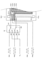
- FIG. 8 is a block diagram showing the configuration of a lighting device 2 according to one embodiment of the present invention.
- the lighting device 2 further includes a switch 50 shown in FIG. 8.
- the switch 50 includes a plurality of contacts (a first contact 510, a second contact 520, a third contact 530, a fourth contact 540, a fifth contact 550, and a sixth contact 560).
- the first contact 510 is electrically connected to one of the third contact 530 and the fourth contact 540
- the second contact 520 is electrically connected to one of the fifth contact 550 and the sixth contact 560.
- the connection of the first contact 510 and the connection of the second contact 520 in the switch 50 are linked.
- the first contact 510 is electrically connected to the third contact 530
- the second contact 520 is electrically connected to the fifth contact 550.
- the first contact 510 is electrically connected to the fourth contact 540
- the second contact 520 is electrically connected to the sixth contact.
- the switch 50 may be, for example, a slide switch, a push switch (alternate switch), or a toggle switch, but is not limited to these.
- the switch 50 may have a configuration that switches the connection of the contacts. For example, when the switch 50 is a push switch, pressing the button switches the connection of the first contact 510 from the third contact 530 to the fourth contact 540. Pressing the button again switches the connection of the first contact 510 from the fourth contact 540 to the third contact 530.
- the switch 50 shown in FIG. 8 is disposed between the control device 30 and the first liquid crystal cell 100-1.
- the first contact 510 is electrically connected to the first terminal 122-1.
- the second contact 520 is electrically connected to the second terminal 122-2.
- the first pulse wave PW1 and the second pulse wave PW2 are input to the third contact 530 and the fifth contact 550, respectively.
- the fixed potential P fix is input to the fourth contact 540 and the sixth contact 560.
- the first pulse wave PW1 and the second pulse wave PW2 are inverted in phase.
- the fixed potential P fix is an arbitrary potential within the range of the amplitude of the first pulse wave PW1 or the second pulse wave PW2.
- the third terminal 122-3 and the fourth terminal 122-4 are input to the third pulse wave PW3 and the fourth pulse wave PW4, respectively.
- the third pulse wave PW3 is the same as the first pulse wave PW1
- the fourth pulse wave PW4 is the same as the second pulse wave PW2.
- the first terminal 122-1, the second terminal 122-2, the third terminal 122-3, and the fourth terminal 122-4 receive the first pulse wave PW1, the second pulse wave PW2, the third pulse wave PW3, and the fourth pulse wave PW4, respectively.
- a transverse electric field is generated between the first transparent electrode 120-1 and the second transparent electrode 120-2 on the first substrate 110-1 of the first liquid crystal cell 100-1, and between the third transparent electrode 120-3 and the fourth transparent electrode 120-4 on the second substrate 110-2. Therefore, the light passing through the first liquid crystal cell 100-1 is isotropically diffused on the first substrate 110-1 side and the second substrate 110-2 side, and has a circular light distribution shape.
- the first contact 510 and the second contact 520 are electrically connected to the fourth contact 540 and the sixth contact 560, respectively. Therefore, a fixed potential P fix is input to the first terminal 122-1 and the second terminal 122-2, and a third pulse wave PW3 and a fourth pulse wave PW4 are input to the third terminal 122-3 and the fourth terminal 122-4, respectively.
- a transverse electric field is not generated between the first transparent electrode 120-1 and the second transparent electrode 120-2 on the first substrate 110-1 of the first liquid crystal cell 100-1, but a transverse electric field is generated between the third transparent electrode 120-3 and the fourth transparent electrode 120-4 on the second substrate 110-2. Therefore, the light passing through the first liquid crystal cell 100-1 is anisotropically diffused only on the second substrate side, and has a linear light distribution shape extending in one direction.
- each of the four switches 50 may be connected to the first liquid crystal cell 100-1 to the fourth liquid crystal cell 100-4, and each of the multiple contacts of one switch may be electrically connected to the first terminal 122-1 to the fourth terminal 122-4 of each of the first liquid crystal cell 100-1 to the fourth liquid crystal cell.
- the connection between the terminals of each liquid crystal cell 100 (the first terminal 122-1 to the fourth terminal 122-4) and the switch 50 may change depending on the light distribution shape. In the lighting device 2, various light distribution shapes can be formed using the switch 50.
- FIG. 9 is a block diagram showing a configuration for generating a pulse wave and a fixed potential in a lighting device 2 according to one embodiment of the present invention.
- the pulse wave and fixed potential input to the contacts of the switch 50 are generated using a control device 30 and a power supply device 40.
- the first control circuit 300-1 outputs the second pulse signal and the third pulse signal in which the phase of the second pulse signal is inverted.
- the first pulse wave PW1 and the second pulse wave PW2 correspond to the second signal and the third signal generated by the first control circuit 300-1, respectively. That is, the first pulse wave PW1 and the second pulse wave PW2 are generated by the first control circuit 300-1.
- the second control circuit 300-2 outputs the second pulse signal and the third pulse signal in which the phase of the second pulse signal is inverted.
- the second signal and the third signal generated by the second control circuit 300-2 correspond to the third pulse wave PW3 and the fourth pulse wave PW4, respectively. That is, the second control circuit 300-2 generates the third pulse wave PW3 and the fourth pulse wave PW4.
- the fixed potential P fix is generated by the third power supply 430. That is, the fixed potential P fix is equal to the center potential.
- the lighting device 2 can generate a pulse wave and a fixed potential without significantly changing the configuration of the control device 30 and the power supply device 40.
- the lighting device 2 can switch the light distribution shape of the light emitted from the light source 20 using the switch 50, without including a DAC or a microcomputer, and can also control the light distribution angle. Therefore, the lighting device 2 can reduce manufacturing costs.
Landscapes
- Physics & Mathematics (AREA)
- Nonlinear Science (AREA)
- Chemical & Material Sciences (AREA)
- Crystallography & Structural Chemistry (AREA)
- General Physics & Mathematics (AREA)
- Optics & Photonics (AREA)
- Mathematical Physics (AREA)
- Spectroscopy & Molecular Physics (AREA)
- Engineering & Computer Science (AREA)
- General Engineering & Computer Science (AREA)
- Liquid Crystal (AREA)
Priority Applications (2)
| Application Number | Priority Date | Filing Date | Title |
|---|---|---|---|
| CN202380090891.1A CN120500661A (zh) | 2023-02-21 | 2023-12-21 | 照明装置 |
| JP2025502138A JPWO2024176604A1 (https=) | 2023-02-21 | 2023-12-21 |
Applications Claiming Priority (4)
| Application Number | Priority Date | Filing Date | Title |
|---|---|---|---|
| JP2023-025289 | 2023-02-21 | ||
| JP2023025289 | 2023-02-21 | ||
| JP2023-072553 | 2023-04-26 | ||
| JP2023072553 | 2023-04-26 |
Publications (1)
| Publication Number | Publication Date |
|---|---|
| WO2024176604A1 true WO2024176604A1 (ja) | 2024-08-29 |
Family
ID=92500962
Family Applications (1)
| Application Number | Title | Priority Date | Filing Date |
|---|---|---|---|
| PCT/JP2023/045907 Ceased WO2024176604A1 (ja) | 2023-02-21 | 2023-12-21 | 照明装置 |
Country Status (3)
| Country | Link |
|---|---|
| JP (1) | JPWO2024176604A1 (https=) |
| CN (1) | CN120500661A (https=) |
| WO (1) | WO2024176604A1 (https=) |
Citations (3)
| Publication number | Priority date | Publication date | Assignee | Title |
|---|---|---|---|---|
| JPS6053933A (ja) * | 1983-09-05 | 1985-03-28 | Canon Inc | 潜像形成装置 |
| JPH08166578A (ja) * | 1994-01-26 | 1996-06-25 | Samsung Electron Co Ltd | 視野角調節機能を具備する液晶表示装置用グレイ電圧発生装置 |
| WO2022176684A1 (ja) * | 2021-02-18 | 2022-08-25 | 株式会社ジャパンディスプレイ | 液晶光制御装置 |
-
2023
- 2023-12-21 JP JP2025502138A patent/JPWO2024176604A1/ja active Pending
- 2023-12-21 CN CN202380090891.1A patent/CN120500661A/zh active Pending
- 2023-12-21 WO PCT/JP2023/045907 patent/WO2024176604A1/ja not_active Ceased
Patent Citations (3)
| Publication number | Priority date | Publication date | Assignee | Title |
|---|---|---|---|---|
| JPS6053933A (ja) * | 1983-09-05 | 1985-03-28 | Canon Inc | 潜像形成装置 |
| JPH08166578A (ja) * | 1994-01-26 | 1996-06-25 | Samsung Electron Co Ltd | 視野角調節機能を具備する液晶表示装置用グレイ電圧発生装置 |
| WO2022176684A1 (ja) * | 2021-02-18 | 2022-08-25 | 株式会社ジャパンディスプレイ | 液晶光制御装置 |
Also Published As
| Publication number | Publication date |
|---|---|
| CN120500661A (zh) | 2025-08-15 |
| JPWO2024176604A1 (https=) | 2024-08-29 |
Similar Documents
| Publication | Publication Date | Title |
|---|---|---|
| JP7716561B2 (ja) | 液晶光制御装置 | |
| JP7649907B2 (ja) | 光学素子 | |
| JP2025023259A (ja) | 光学素子および照明装置 | |
| US20240310679A1 (en) | Optical element | |
| US11754904B2 (en) | Light control device and illumination device | |
| WO2024176604A1 (ja) | 照明装置 | |
| US12248227B2 (en) | Method for driving optical element | |
| US11940710B2 (en) | Light control device and illumination device | |
| JP7802197B2 (ja) | 光学素子および照明装置 | |
| JP7622219B2 (ja) | 光学装置 | |
| JP7796893B2 (ja) | 照明装置 | |
| WO2024252853A1 (ja) | 照明装置 | |
| CN120225949A (zh) | 照明装置 | |
| US20260085815A1 (en) | Lighting device | |
| JP7733838B2 (ja) | 照明システム | |
| US20240361649A1 (en) | Optical element | |
| JP7738776B2 (ja) | 照明装置とその駆動方法 | |
| US20250155758A1 (en) | Optical device | |
| HK40099657A (zh) | 光学装置 | |
| CA3236383A1 (en) | Lighting device | |
| CN117130180A (zh) | 光学元件以及显示装置 |
Legal Events
| Date | Code | Title | Description |
|---|---|---|---|
| 121 | Ep: the epo has been informed by wipo that ep was designated in this application |
Ref document number: 23924248 Country of ref document: EP Kind code of ref document: A1 |
|
| WWE | Wipo information: entry into national phase |
Ref document number: 2025502138 Country of ref document: JP |
|
| WWE | Wipo information: entry into national phase |
Ref document number: 202380090891.1 Country of ref document: CN |
|
| WWP | Wipo information: published in national office |
Ref document number: 202380090891.1 Country of ref document: CN |
|
| NENP | Non-entry into the national phase |
Ref country code: DE |
|
| 122 | Ep: pct application non-entry in european phase |
Ref document number: 23924248 Country of ref document: EP Kind code of ref document: A1 |