WO2024176297A1 - 磁壁移動素子及び磁気アレイ - Google Patents
磁壁移動素子及び磁気アレイ Download PDFInfo
- Publication number
- WO2024176297A1 WO2024176297A1 PCT/JP2023/005968 JP2023005968W WO2024176297A1 WO 2024176297 A1 WO2024176297 A1 WO 2024176297A1 JP 2023005968 W JP2023005968 W JP 2023005968W WO 2024176297 A1 WO2024176297 A1 WO 2024176297A1
- Authority
- WO
- WIPO (PCT)
- Prior art keywords
- layer
- domain wall
- ferromagnetic
- wall motion
- motion element
- Prior art date
- Legal status (The legal status is an assumption and is not a legal conclusion. Google has not performed a legal analysis and makes no representation as to the accuracy of the status listed.)
- Ceased
Links
Images








Classifications
-
- G—PHYSICS
- G11—INFORMATION STORAGE
- G11C—STATIC STORES
- G11C11/00—Digital stores characterised by the use of particular electric or magnetic storage elements; Storage elements therefor
- G11C11/02—Digital stores characterised by the use of particular electric or magnetic storage elements; Storage elements therefor using magnetic elements
- G11C11/16—Digital stores characterised by the use of particular electric or magnetic storage elements; Storage elements therefor using magnetic elements using elements in which the storage effect is based on magnetic spin effect
-
- H—ELECTRICITY
- H10—SEMICONDUCTOR DEVICES; ELECTRIC SOLID-STATE DEVICES NOT OTHERWISE PROVIDED FOR
- H10B—ELECTRONIC MEMORY DEVICES
- H10B61/00—Magnetic memory devices, e.g. magnetoresistive RAM [MRAM] devices
-
- H—ELECTRICITY
- H10—SEMICONDUCTOR DEVICES; ELECTRIC SOLID-STATE DEVICES NOT OTHERWISE PROVIDED FOR
- H10D—INORGANIC ELECTRIC SEMICONDUCTOR DEVICES
- H10D48/00—Individual devices not covered by groups H10D1/00 - H10D44/00
- H10D48/40—Devices controlled by magnetic fields
Definitions
- the present invention relates to a domain wall motion element and a magnetic array.
- Magnetoresistive effect elements are known that utilize a change in resistance value (magnetoresistance change) based on a change in the relative angle between the magnetizations of two ferromagnetic layers.
- the domain wall motion type magnetoresistive effect element (hereinafter referred to as domain wall motion element) described in Patent Document 1 is one example of a magnetoresistive effect element.
- domain wall motion elements the resistance value in the stacking direction changes depending on the position of the domain wall, and data can be recorded in multi-value or analog form.
- the magnetic domain wall motion element can be used in neuromorphic devices that mimic the functions of the brain, as described in Patent Document 2, for example.
- the domain wall of the domain wall motion element moves when a torque is applied to the magnetization of the ferromagnetic layer, causing a portion of the magnetization of the ferromagnetic layer to reverse.
- Spin transfer torque (STT) and spin orbit torque (SOT) are examples of torques applied to the magnetization of the ferromagnetic layer.
- Spin transfer torque is generated when a current flows in a direction intersecting the domain wall.
- Spin orbit torque is generated when spins are injected from a layer adjacent to the ferromagnetic layer having the domain wall.
- Spin orbit torque is easily affected by external magnetic fields, environmental temperature, etc., and its characteristics are easily changed depending on the environment.
- the characteristics of the domain wall motion element are likely to vary depending on the environment. Changes in the characteristics of the domain wall motion element due to changes in the environment reduce the reliability of the domain wall motion element.
- This disclosure has been made in consideration of the above problems, and aims to provide a domain wall motion element and magnetic array that reduce the contribution of spin-orbit torque to magnetization reversal.
- the domain wall motion element includes a laminate.
- the laminate includes a first ferromagnetic layer, a second ferromagnetic layer, and a spacer layer sandwiched between the first ferromagnetic layer and the second ferromagnetic layer. At least one of the first ferromagnetic layer and the second ferromagnetic layer has a domain wall therein.
- the spacer layer includes a nonmagnetic first layer and a nonmagnetic second layer adjacent to the first layer. The first layer exhibits a negative spin Hall angle, and the second layer exhibits a positive spin Hall angle. A portion of the write current flows along any direction within the plane of the spacer layer.
- FIG. 2 is a block diagram of a magnetic array according to the first embodiment.
- FIG. 2 is a circuit diagram of an integrated region of the magnetic array according to the first embodiment.
- 3 is a cross-sectional view of the vicinity of a domain wall motion element of the magnetic array according to the first embodiment.
- FIG. 1 is a cross-sectional view of a domain wall motion element according to a first embodiment.
- FIG. 2 is a plan view of the domain wall motion element according to the first embodiment. 3 is an enlarged view of a characteristic portion of the domain wall motion element according to the first embodiment.
- FIG. 1 is a cross-sectional view of a domain wall motion element according to a first embodiment.
- FIG. 2 is a plan view of the domain wall motion element according to the first embodiment.
- 3 is an enlarged
- FIG. 11 is a cross-sectional view of a domain wall motion element according to a second embodiment. 13 is an enlarged view of a characteristic portion of the domain wall motion element according to the second embodiment. FIG. 13 is an enlarged view of a characteristic portion of another example of the domain wall motion element according to the second embodiment.
- FIG. FIG. 11 is a cross-sectional view of a domain wall motion element according to a third embodiment. 13 is an enlarged view of a characteristic portion of the domain wall motion element according to the third embodiment.
- FIG. This shows an example of how magnetization twists in a domain wall that occurs between two magnetic domains.
- FIG. 2 is a conceptual diagram of the Dzyaloshinskii-Moriya interaction acting between a nonmagnetic layer and a ferromagnetic layer. 13 is an enlarged view of a characteristic portion of another example of the domain wall motion element according to the third embodiment.
- FIG. FIG. 13 is a cross-sectional view of a domain wall motion element according to a fourth embodiment.
- the directions are defined.
- the x and y directions are approximately parallel to one surface of the substrate Sub (see FIG. 3), which will be described later.
- the x direction is the direction in which the laminate, which will be described later, extends.
- the y direction is perpendicular to the x direction.
- the z direction is the direction from the substrate, which will be described later, to the domain wall motion element.
- the +z direction may be expressed as "up” and the -z direction as "down”, but these expressions are for convenience and do not define the direction of gravity.
- "extending in the x direction” means, for example, that the dimension in the x direction is larger than the smallest dimension among the dimensions in the x, y, and z directions. The same applies to extending in other directions.
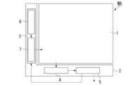
- FIG. 1 is a block diagram of a magnetic array MA according to a first embodiment.
- the magnetic array MA has an integration region 1 and a peripheral region 2.
- the magnetic array MA can be used for, for example, a magnetic memory, a multiply-accumulate calculator, a neuromorphic device, a spin memristor, or a magneto-optical element.
- the accumulation region 1 is an area where multiple domain wall motion elements are accumulated.
- the magnetic array MA is used as a memory, data is stored in the accumulation region 1.
- the magnetic array MA is used as a neuromorphic device, learning and inference are performed in the accumulation region 1.
- the peripheral region 2 is an area in which a control element that controls the operation of the domain wall motion element in the integration region 1 is implemented.
- the peripheral region 2 includes, for example, a pulse application device 3, a resistance detection device 4, and an output section 5.
- the pulse application device 3 is configured to apply a pulse to at least one of the multiple domain wall motion elements in the accumulation region 1.
- the pulse application device 3 has, for example, a control unit 6 and a power supply 7.
- the control unit 6 has, for example, a processor and a memory.
- the processor is, for example, a CPU (Central Processing Unit).
- the processor operates based on an operating program stored in the memory.
- the control unit 6 controls, for example, the address of the domain wall motion element to which a pulse is applied, the magnitude of the pulse (voltage, pulse length) to be applied to a specific domain wall motion element, etc.
- the control unit 6 may also have a clock, a counter, a random number generator, etc.
- the clock is an indicator of the timing to apply the pulse, and the counter counts the number of times the pulse is applied, etc.
- the power supply 7 applies a pulse to the domain wall motion element according to instructions from the control unit 6.
- the resistance detection device 4 is configured to detect the resistance value of the domain wall motion elements in the integration region 1.
- the resistance detection device 4 may detect the resistance of each domain wall motion element in the integration region 1, or may detect the total resistance of domain wall motion elements belonging to the same column, for example.
- the resistance detection device 4 has, for example, a comparator that compares the magnitude of the detected resistance values.
- the comparator may, for example, compare the detected resistance values with each other, or may compare the detected resistance value with a preset reference resistance value.
- the output unit 5 is connected to the resistance detection device 4.
- the output unit 5 has, for example, a processor, an output capacitor, an amplifier, a converter, etc.
- the output unit 5 may perform a calculation to substitute the detection result of the resistance detection device 4 into an activation function. The calculation is performed, for example, by a processor.
- the output unit 5 outputs the calculation result to the outside.
- the calculation result may be output as an input signal for another magnetic array, or may be output to the outside as a discrimination rate.
- the output unit 5 may also feed back the calculation result to the pulse application device 3.
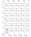
- FIG. 2 is a circuit diagram of the integrated region 1 according to the first embodiment.
- the integrated region 1 includes a plurality of domain wall motion elements 100, a plurality of first wirings WL, a plurality of second wirings CL, a plurality of third wirings RL, a plurality of first switching elements SW1, and a plurality of second switching elements SW2.
- the third switching element SW3 may belong to, for example, the pulse application device 3 in the peripheral region 2.
- the multiple domain wall motion elements 100 are arranged, for example, in a matrix.
- the multiple domain wall motion elements 100 are not limited to elements arranged in a matrix in the actual device, but may be arranged in a matrix in a circuit diagram.
- Each of the first wirings WL is a write wiring. Each of the first wirings WL electrically connects the pulse application device 3 to one or more domain wall motion elements 100.
- Each of the second wirings CL is a common wiring that can be used both when writing and reading data. Each of the second wirings CL is connected to, for example, the resistance detection device 4. The second wirings CL may be provided in each of the multiple domain wall motion elements 100, or may be provided across the multiple domain wall motion elements 100.
- Each of the third wirings RL is a read wiring. Each of the third wirings RL electrically connects the pulse application device 3 to one or more domain wall motion elements 100.
- the first switching element SW1, the second switching element SW2, and the third switching element SW3 are elements that control the flow of current.
- the first switching element SW1, the second switching element SW2, and the third switching element SW3 are, for example, elements that utilize a phase change in a crystal layer such as a transistor or an Ovonic Threshold Switch (OTS), elements that utilize a change in band structure such as a Metal-Insulator Transition (MIT) switch, elements that utilize a breakdown voltage such as a Zener diode or an avalanche diode, and elements whose conductivity changes with a change in atomic position.
- OTS Ovonic Threshold Switch
- MIT Metal-Insulator Transition
- the first switching element SW1 and the second switching element SW2 are connected, for example, to each of the domain wall motion elements 100.
- the first switching element SW1 is connected, for example, between the domain wall motion element 100 and the first wiring WL.
- the second switching element SW2 is connected, for example, between the domain wall motion element 100 and the second wiring CL.
- the third switching element SW3 is connected, for example, across multiple domain wall motion elements 100.
- the third switching element SW3 is connected, for example, to the third wiring RL.
- the positional relationship between the first switching element SW1, the second switching element SW2, and the third switching element SW3 is not limited to that shown in FIG. 2.
- the first switching element SW1 may be connected across multiple domain wall motion elements 100 and located upstream of the first wiring WL.
- the second switching element SW2 may be connected across multiple domain wall motion elements 100 and located upstream of the second wiring CL.
- the third switching element SW3 may be connected to each domain wall motion element 100 one by one.
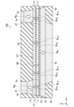
- FIG. 3 is a cross-sectional view of the vicinity of the domain wall motion element 100 in the integration region 1 according to the first embodiment.
- FIG. 3 is a cross-section of one domain wall motion element 100 in FIG. 2 cut along the xz plane passing through the center of the width of the stack 10 in the y direction.
- the first switching element SW1 and the second switching element SW2 shown in FIG. 3 are transistors Tr.
- the transistor Tr has a gate electrode G, a gate insulating film GI, and a source S and a drain D formed on a substrate Sub.
- the source S and the drain D are determined by the direction of current flow, and are both active regions of a semiconductor.
- FIG. 3 shows only one example, and the positional relationship between the source S and the drain D may be reversed.
- the substrate Sub is, for example, a semiconductor substrate.
- the third switching element SW3 is electrically connected to the third wiring RL, and is, for example, shifted in the y direction in FIG. 3.
- the transistor Tr, the first wiring WL, the second wiring CL, the third wiring RL, and the domain wall motion element 100 are connected by via wiring Vw extending in the z direction or in-plane wiring IPw extending in any direction within the xy plane.
- the via wiring Vw and the in-plane wiring IPw contain a conductive material.
- An insulating layer 90 is formed between different layers in the z direction, except for the via wiring Vw.
- the insulating layer 90 is an insulating layer that insulates between wirings of a multilayer wiring and between elements.
- the domain wall motion element 100 and the transistor Tr are electrically isolated by the insulating layer 90, except for the via wiring Vw.
- the insulating layer 90 is, for example, silicon oxide (SiO x ), silicon nitride (SiN x ), silicon carbide (SiC), chromium nitride, silicon carbonitride (SiCN), silicon oxynitride (SiON), aluminum oxide (Al 2 O 3 ), zirconium oxide (ZrO x ), or the like.
- FIG. 4 is a cross-sectional view of the domain wall motion element 100 cut in the xz plane passing through the center of the stack 10 in the y direction.
- the arrows in the figure are an example of the orientation direction of magnetization of a ferromagnetic material.
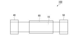
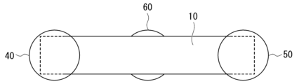
- FIG. 5 is a plan view of the domain wall motion element 100 as seen from the z direction.
- the domain wall motion element 100 includes, for example, a stack 10, a non-magnetic layer 20, a reference layer 30, a magnetization fixed layer 40, a magnetization fixed layer 50, and an electrode 60. At least one of the multiple domain wall motion elements included in the accumulation region 1 is the domain wall motion element 100 shown in Figures 4 and 5.
- the laminate 10 When viewed from the z direction, the length of the laminate 10 in the x direction is longer than its length in the y direction.
- the laminate 10 includes, for example, a first ferromagnetic layer 11, a second ferromagnetic layer 12, and a spacer layer 13.
- the magnetization of the first ferromagnetic layer 11 is magnetically coupled to the magnetization of the second ferromagnetic layer 12. Therefore, the laminate 10 as a whole can also be regarded as a single ferromagnetic layer.
- the laminate 10 has two different magnetic domains, and a domain wall DW at the boundary between the two magnetic domains.
- the domain wall DW moves in the x-direction inside the laminate 10.
- the laminate 10 is a layer that can magnetically record information by changing the magnetic state.
- the laminate 10 is also called a domain wall displacement layer, analog layer, free layer, or magnetic recording layer.
- the laminate 10 has a first region A1, a second region A2, and a third region A3.
- the laminate 10 includes a domain wall motion region in which the domain wall DW can move in the x direction, and a magnetization fixed region in which the magnetization is fixed.
- the first region A1 is a region in which the orientation direction of magnetization is fixed in one direction.
- the first region A1 is an example of a magnetization fixed region.
- the magnetization being fixed means that the magnetization does not reverse during normal operation of the domain wall motion element 100 (when no external force exceeding the expected value is applied).
- the first region A1 is, for example, a region of the stack 10 that overlaps with the magnetization fixed layer 40 when viewed from the z direction.
- the magnetization of the first region A1 is fixed by, for example, the magnetization M40 of the magnetization fixed layer 40.
- the second region A2 is a region in which the magnetization orientation direction is fixed in one direction.
- the second region A2 is an example of a magnetization fixed region.
- the magnetization orientation direction of the second region A2 is different from that of the first region A1.
- the magnetization orientation direction of the second region A2 is, for example, opposite to that of the first region A1.
- the second region A2 is, for example, a region of the stack 10 that overlaps with the magnetization fixed layer 50 when viewed from the z direction.
- the magnetization of the second region A2 is fixed, for example, by the magnetization M50 of the magnetization fixed layer 50.
- the third region A3 is a region other than the first region A1 and the second region A2 of the laminate 10.
- the third region A3 is, for example, a region sandwiched between the first region A1 and the second region A2 in the x direction.
- the third region A3 is a region where the magnetization direction changes and the domain wall DW can move.
- the third region A3 is an example of a domain wall movable region.
- the third region A3 has a first magnetic domain and a second magnetic domain.
- the first magnetic domain and the second magnetic domain have opposite magnetization orientation directions.
- the boundary between the first magnetic domain and the second magnetic domain is the domain wall DW.
- the magnetization M 11A , the magnetization M 12A , the magnetization M 11C , and the magnetization M 12C belong to, for example, the first magnetic domain.
- the magnetization M 11B , the magnetization M 12B , the magnetization M 11D , and the magnetization M 12D belong to, for example, the second magnetic domain.
- the domain wall DW moves within the third region A3 and does not invade the first region A1 and the second region A2.
- the domain wall DW moves.
- the domain wall DW moves, for example, by passing a write current in the x direction of the third region A3.
- the first ferromagnetic layer 11 and the second ferromagnetic layer 12 include a magnetic material.
- the first ferromagnetic layer 11 is, for example, closer to the nonmagnetic layer 20 than the second ferromagnetic layer 12.
- At least one of the first ferromagnetic layer 11 and the second ferromagnetic layer 12 has a domain wall DW therein.
- Both the first ferromagnetic layer 11 and the second ferromagnetic layer 12 may have a domain wall DW therein.
- the first ferromagnetic layer 11 may have a domain wall DW therein and include a domain wall motion region where the domain wall DW can move and a magnetization fixed region where magnetization is fixed.
- the second ferromagnetic layer 12 may have a domain wall DW therein and include a domain wall motion region where the domain wall DW can move and a magnetization fixed region where magnetization is fixed.
- the domain wall motion region is a portion belonging to the third region A3, and the magnetization fixed region is a portion belonging to the first region A1 or the second region A2.
- the magnetization of the first ferromagnetic layer 11 is magnetically coupled to the magnetization of the second ferromagnetic layer 12.
- the first ferromagnetic layer 11 reflects the magnetic state of the second ferromagnetic layer 12.
- the magnetic states of the first ferromagnetic layer 11 and the second ferromagnetic layer 12 are the same, and when the first ferromagnetic layer 11 and the second ferromagnetic layer 12 are antiferromagnetically coupled, the magnetic states of the first ferromagnetic layer 11 and the second ferromagnetic layer 12 are opposite.
- the first ferromagnetic layer 11 and the second ferromagnetic layer 12 each contain at least one element selected from the group consisting of, for example, Co, Ni, Fe, Pt, Pd, Gd, Tb, Mn, Ge, and Ga.
- the first ferromagnetic layer 11 and the second ferromagnetic layer 12 may be made of the same or different materials. Since the first ferromagnetic layer 11 and the second ferromagnetic layer 12 have different required functions, it is preferable that the first ferromagnetic layer 11 and the second ferromagnetic layer 12 be made of different materials.
- the first ferromagnetic layer 11 sandwiches the nonmagnetic layer 20 together with the reference layer 30.
- the magnetic resistance change of the domain wall motion element 100 occurs due to a change in the relative angle of magnetization of the two ferromagnetic layers sandwiching the nonmagnetic layer 20.
- the first ferromagnetic layer 11 has a greater effect on the MR ratio of the domain wall motion element 100 than the second ferromagnetic layer 12. Therefore, the first ferromagnetic layer 11 is required to be made of a material that can increase the MR ratio of the domain wall motion element 100.
- the first ferromagnetic layer 11 is, for example, CoFeB.
- the second ferromagnetic layer 12 has a smaller effect on the MR ratio of the domain wall motion element 100 than the first ferromagnetic layer 11. Therefore, a material that is easy to control the movement of the domain wall DW can be selected for the second ferromagnetic layer 12.
- the second ferromagnetic layer 12 is, for example, a laminated film of Co and Ni, a laminated film of Co and Pt, a laminated film of Co and Pd, a MnGa-based material, a GdCo-based material, a TbCo-based material, etc.
- Ferrimagnetic materials such as MnGa-based materials, GdCo-based materials, and TbCo-based materials have small saturation magnetization, and the threshold current required to move the domain wall DW is small.
- a laminated film of Co and Ni, a laminated film of Co and Pt, and a laminated film of Co and Pd have a large coercive force, and the movement speed of the domain wall DW is slow.
- the thickness h11 of the first ferromagnetic layer 11 and the thickness h12 of the second ferromagnetic layer 12 may be the same or different.
- the thickness h12 of the second ferromagnetic layer 12 may be thicker than the thickness h11 of the first ferromagnetic layer 11.
- the spin orbit torque is generated by the injection of spins from the interface with the adjacent layer. If the thickness h12 of the second ferromagnetic layer 12 is thick, the contribution of the spin orbit torque to the magnetization reversal of the second ferromagnetic layer 12 becomes smaller.
- the second ferromagnetic layer 12 has a larger effect on the movement of the domain wall DW than the first ferromagnetic layer 11. In other words, if the thickness h12 of the second ferromagnetic layer 12 is thick, the contribution of the spin orbit torque to the movement of the domain wall DW becomes smaller.
- the spacer layer 13 is between the first ferromagnetic layer 11 and the second ferromagnetic layer 12.
- the spacer layer 13 magnetically couples the first ferromagnetic layer 11 and the second ferromagnetic layer 12.
- the spacer layer 13 is also called a magnetic coupling layer or an intermediate layer.
- the spacer layer 13 includes a nonmagnetic material.
- the thickness of the spacer layer 13 is, for example, 2 nm or less, and preferably 1 nm or less.
- FIG. 6 is an enlarged view of a characteristic portion of the domain wall motion element according to the first embodiment.
- the spacer layer 13 has, for example, a first layer 14 and a second layer 15.
- the first layer 14 and the second layer 15 are adjacent to each other. Both the first layer 14 and the second layer 15 are non-magnetic layers.
- the first layer 14 exhibits a negative spin Hall angle
- the second layer 15 exhibits a positive spin Hall angle.
- the positional relationship between the first layer 14 and the second layer 15 may be reversed.
- the first layer 14 and the second layer 15 have different signs (polarities) of the spin Hall angle.
- the "spin Hall angle” is one of the indices of the strength of the spin Hall effect, and indicates the conversion efficiency of the spin current with respect to the write current.
- the sign (polarity) of the spin Hall angle means the positive or negative value, and is "+" or "-”.
- a part of the write current flows at least along the spacer layer 13.
- the write current flows through the first ferromagnetic layer 11 and the second ferromagnetic layer 12 in addition to the spacer layer 13.
- the write current flows in parallel through the first ferromagnetic layer 11, the second ferromagnetic layer 12, and the spacer layer 13.
- the spin Hall effect is a phenomenon in which, when electric current is passed, a spin current is induced in a direction perpendicular to the direction of electric current flow due to spin-orbit interaction.
- the spin Hall effect is similar to the regular Hall effect in that the direction of movement of moving charges (electrons) can be bent.
- the regular Hall effect the direction of movement of charged particles moving in a magnetic field is bent by the Lorentz force.
- the direction of spin movement can be bent simply by the movement of electrons (the flow of electric current) even in the absence of a magnetic field.
- spins sp oriented in the +y direction are unevenly distributed on the first surface 14A of the first layer 14, and spins sp oriented in the -y direction are unevenly distributed on the second surface 14B.
- spins sp oriented in the -y direction for example, are unevenly distributed on the first surface 15A of the second layer 15, and spins sp oriented in the +y direction are unevenly distributed on the second surface 15B.
- a spin current is generated in the z direction to eliminate the uneven distribution of these spins (spin polarization).
- spin polarities of the spin Hall angles are different, the positive and negative of the spins unevenly distributed on the first and second surfaces are reversed.
- the first layer 14 and the second layer 15 have different signs of the spin Hall angle. Therefore, when considering the spacer layer 13 as a whole, the spin current generated in the first layer 14 and the spin current generated in the second layer 15 cancel each other out. As a result, the amount of spin injected into the first ferromagnetic layer 11 or the second ferromagnetic layer 12 is reduced. In other words, when the first layer 14 and the second layer 15 have different signs of the spin Hall angle, the contribution of the spin orbit torque to the magnetization reversal of the first ferromagnetic layer 11 or the second ferromagnetic layer 12 is reduced.
- the sign of the spin Hall angle is determined by the electronic state of the layer, and therefore varies with the material that constitutes the layer, the thickness of the layer, adjacent materials, etc.
- the sign of the material that constitutes the layer may change when multiple elements are dissolved in a solid solution, such as an alloy, or the polarity may change when the material is compounded, such as by oxidation, nitridation, or carbonization.
- the sign may also change by changing the macroscopic electronic state by stacking different materials.
- the sign of the spin Hall angle may also change depending on the thickness of the layer.
- the spacer layer 13 contains, for example, any atom selected from the group consisting of Mg, Au, Al, Hf, Ta, W, Mo, Pt, Pd, Cu, Ru, and Ir.
- the first layer 14 contains, for example, atoms belonging to any one of groups 3, 4, 5, and 6.
- the first layer 14 mainly contains, for example, metal elements belonging to any one of groups 3, 4, 5, and 6. "Mainly" indicates that the content of these metal elements is 50 atm % or more.
- the sign of the spin Hall angle is not determined solely by the material, but when the first layer 14 contains these materials, the first layer 14 tends to exhibit a negative spin Hall angle.
- the first layer 14 is, for example, Ta.
- the first layer 14 may also contain any of oxygen, nitrogen, and carbon.
- the first layer 14 may be, for example, any of an oxide, nitride, and carbide of a metal belonging to any of Groups 3, 4, 5, and 6.
- the first layer 14 may be tantalum nitride (TaN).
- the second layer 15 contains, for example, atoms belonging to any one of groups 8, 9, 10, 11, and 12.
- the second layer 15 contains, for example, mainly atoms belonging to any one of groups 8, 9, 10, 11, and 12.
- the sign of the spin Hall angle is not determined solely by the material, but when the second layer 15 contains these materials, the second layer 15 tends to exhibit a positive spin Hall angle.
- the second layer 15 is, for example, Pt.
- the second layer 15 may also contain oxygen, nitrogen, or carbon.
- the second layer 15 may be, for example, an oxide, nitride, or carbide of a metal belonging to any of groups 8, 9, 10, 11, and 12.
- the thickness of the first layer 14 may be the same as or different from the thickness of the second layer 15.
- Figure 7 is an enlarged view of another example of a characteristic portion of the domain wall motion element according to the first embodiment.
- the thickness h15 of the second layer 15 shown in Figure 7 is thicker than the thickness h14 of the first layer 14.
- the thickness of the layer having the larger absolute value of the spin Hall angle between the first layer 14 and the second layer 15 is thinner than the thickness of the layer having the smaller absolute value of the spin Hall angle between the first layer 14 and the second layer 15.
- the second layer 15 shown in FIG. 7 has a smaller absolute value of the spin Hall angle than the first layer 14. The larger the absolute value of the spin Hall angle, the stronger the spin Hall effect.
- the thickness of the layer having the higher resistivity between the first layer 14 and the second layer 15 is thicker than the thickness of the layer having the lower resistivity between the first layer 14 and the second layer 15.
- the second layer 15 shown in FIG. 7 has a higher resistivity than the first layer 14.
- each of the first layer 14 and the second layer 15 is, for example, 0.1 nm or more and 20 nm or less.
- the non-magnetic layer 20 is sandwiched between the stack 10 and the reference layer 30.
- the non-magnetic layer 20 is laminated on one side of the reference layer 30.
- the nonmagnetic layer 20 is made of, for example, a nonmagnetic insulator, semiconductor, or metal.
- the nonmagnetic layer 20 is preferably, for example, a nonmagnetic insulator.
- the nonmagnetic insulator is, for example, Al 2 O 3 , SiO 2 , MgO, MgAl 2 O 4 , and materials in which a part of Al, Si, and Mg is replaced with Zn, Be, or the like. These materials have a large band gap and excellent insulating properties.
- the nonmagnetic insulator is, for example, an oxide containing Mg or Al.
- the nonmagnetic layer 20 is a tunnel barrier layer.
- the nonmagnetic metal is, for example, Cu, Au, Ag, or the like.
- the nonmagnetic semiconductor is, for example, Si, Ge, CuInSe 2 , CuGaSe 2 , Cu(In,Ga)Se 2 , or the like.
- the thickness of the nonmagnetic layer 20 is, for example, 20 ⁇ or more, and may be 25 ⁇ or more.
- the reference layer 30 is located so that at least a portion of it overlaps with the third region A3 in the z-direction.
- the reference layer 30 is, for example, closer to the substrate Sub than the stack 10.
- the magnetization of the reference layer 30 is less likely to reverse than the magnetization of the third region A3 of the laminate 10.
- the magnetization of the reference layer 30 is fixed and does not change direction when an external force strong enough to reverse the magnetization of the third region A3 is applied.
- the reference layer 30 is sometimes referred to as a fixed layer.
- the reference layer 30 includes a ferromagnetic material.
- the reference layer 30 includes, for example, a material that is likely to produce a coherent tunnel effect between the layered body 10 and the reference layer 30.
- the reference layer 30 includes, for example, a metal selected from the group consisting of Cr, Mn, Co, Fe, and Ni, an alloy containing one or more of these metals, an alloy containing these metals and at least one of the elements B, C, and N, and the like.
- the reference layer 30 is, for example, Co-Fe, Co-Fe-B, or Ni-Fe.
- the reference layer 30 may be, for example, a Heusler alloy.
- the Heusler alloy is a half metal and has high spin polarizability.
- the Heusler alloy is an intermetallic compound having a chemical composition of XYZ or X 2 YZ, where X is a transition metal element or a noble metal element of the Co, Fe, Ni, or Cu group on the periodic table, Y is a transition metal element or an element type of X of the Mn, V, Cr, or Ti group, and Z is a typical element of the III group to the V group.
- Examples of Heusler alloys include Co 2 FeSi, Co 2 FeGe, Co 2 FeGa, Co 2 MnSi, Co 2 Mn 1-a Fe a Al b Si 1-b , and Co 2 FeGe 1-c Gac .
- the reference layer 30 and the non-magnetic layer 20 are each longer than the third region A3 in the x direction, for example.
- the portion where the reference layer 30 and the third region A3 face each other with the non-magnetic layer 20 in between is responsible for the resistance change of the domain wall motion element 100. If the length of the reference layer 30 and the non-magnetic layer 20 in the x direction is longer than the length of the third region in the x direction, it becomes easier to divide the resistance change width of the domain wall motion element 100 into multiple values.
- the reference layer 30 is, for example, longer than the stack 10 in the x direction.
- the heat dissipation of the stack 10 is improved.
- the stability of the magnetization of the first region A1 and the magnetization of the second region A2 is increased, and the reliability of the data of the domain wall motion element 100 is improved.
- the magnetization fixed layer 40 is connected to the stack 10.
- the magnetization fixed layer 40 is connected to the first region A1 of the stack 10.
- the magnetization M40 of the magnetization fixed layer 40 fixes the magnetization of the first region A1.
- the magnetization fixed layer 40 is a write electrode used when applying a write current to the domain wall motion element 100. The write current flows between the magnetization fixed layer 40 and the magnetization fixed layer 50.
- the magnetization fixed layer 40 is, for example, a ferromagnetic material.
- the same material as the first ferromagnetic layer 11, the second ferromagnetic layer 12, or the reference layer 30 can be used for the magnetization fixed layer 40.
- the magnetization fixed layer 40 may also have multiple layers and may be a synthetic antiferromagnetic structure (SAF structure).
- the synthetic antiferromagnetic structure consists of two magnetic layers sandwiching a nonmagnetic spacer layer.
- the magnetic layers include, for example, a ferromagnetic material and may include an antiferromagnetic material such as IrMn or PtMn.
- the spacer layer includes, for example, at least one selected from the group consisting of Ru, Ir, and Rh.
- the magnetization fixed layer 40 is not limited to a ferromagnetic material. If the magnetization fixed layer 40 is not a ferromagnetic material, the current density of the current flowing through the stack 10 changes suddenly in the region overlapping with the magnetization fixed layer 40, restricting the movement of the domain wall DW and fixing the magnetization of the first region A1.
- the magnetization fixed layer 50 is connected to the stack 10 at a position different from that of the magnetization fixed layer 40.
- the magnetization fixed layer 50 is connected to the second region A2 of the stack 10.
- the magnetization M50 of the magnetization fixed layer 50 fixes the magnetization of the second region A2.
- the magnetization fixed layer 50 is a common electrode used when applying a write current to the domain wall motion element 100 and when applying a read current to the domain wall motion element 100.
- the magnetization fixed layer 50 can be made of the same material as the magnetization fixed layer 40.
- the magnetization fixed layer 50 may also be a synthetic antiferromagnetic structure (SAF structure).
- the film thickness of the magnetization fixed layer 50 may be thicker than the film thickness of the magnetization fixed layer 40. If the film thickness of the magnetization fixed layer 50 differs from that of the magnetization fixed layer 40, a difference in coercivity is likely to occur between the magnetization fixed layer 50 and the magnetization fixed layer 40. If there is a difference in coercivity between the magnetization fixed layer 50 and the magnetization fixed layer 40, it becomes easier to set the orientation direction of the magnetization M50 of the magnetization fixed layer 50 and the orientation direction of the magnetization M40 of the magnetization fixed layer 40 to different directions at the time of manufacture.
- the shape of the magnetization fixed layer 40 and the magnetization fixed layer 50 is not particularly important.
- FIG. 5 shows an example in which the planar shape of the magnetization fixed layer 40 and the magnetization fixed layer 50 as viewed from the z direction is rectangular, but as shown in FIG. 8, the planar shape of the magnetization fixed layer 40 and the magnetization fixed layer 50 may be circular.
- FIG. 8 is a plan view of another example of the domain wall motion element 100 according to the first embodiment.
- the planar shape of the magnetization fixed layer 40 and the magnetization fixed layer 50 is, for example, rectangular, circular, elliptical, etc.
- the electrode 60 is connected to the reference layer 30.
- the electrode 60 is a read electrode used when applying a read current to the domain wall motion element 100.
- the read current flows, for example, between the magnetization fixed layer 50 and the electrode 60.
- the electrode 60 includes a material having electrical conductivity.
- the electrode 60 may be a via wiring extending in the z direction.
- the domain wall motion element 100 may have layers other than the stack 10, the nonmagnetic layer 20, and the reference layer 30.
- a magnetic layer may be provided on the surface of the reference layer 30 opposite the nonmagnetic layer 20, via a spacer layer.
- the reference layer 30, the spacer layer, and the magnetic layer form a synthetic antiferromagnetic structure (SAF structure).
- a base layer may be provided on the surface of the magnetic layer opposite the spacer layer.
- the magnetization direction of each layer of the domain wall motion element 100 can be confirmed, for example, by measuring the magnetization curve.
- the magnetization curve can be measured, for example, using MOKE (Magneto Optical Kerr Effect). Measurement using MOKE is a measurement method in which linearly polarized light is incident on the object to be measured, and the magneto-optical effect (magnetic Kerr effect) is used to cause the polarization direction to rotate, etc.
- MOKE Magnetic Optical Kerr Effect
- the domain wall motion element 100 is formed by a process of stacking each layer and a process of processing a part of each layer into a predetermined shape.
- the layers can be stacked using a sputtering method, a chemical vapor deposition (CVD) method, an electron beam deposition method (EB deposition method), an atomic laser deposition method, etc.
- the layers can be processed using photolithography and etching (e.g., Ar etching), etc.
- the write operation is performed, for example, by a processor executing an operation program stored in the control unit 6.
- the pulse application device 3 selects the domain wall motion element 100 to which a pulse is to be applied in accordance with the operating program.
- the domain wall motion element 100 to which a pulse is applied is an element that stores data.
- the domain wall motion element 100 to which a pulse is applied is an element that changes the weight in response to learning.
- the control unit 6 controls which of the multiple domain wall motion elements 100 to apply a pulse to.
- the control unit 6 turns ON the first switching element SW1 and second switching element SW2 connected to the domain wall motion element 100 to which the pulse is to be applied, and turns OFF the third switching element SW3.
- the control unit 6 also turns OFF at least one of the first switching element SW1 and second switching element SW2 connected to the domain wall motion element 100 to which the pulse is not to be applied.
- the pulse application device 3 outputs a write pulse to the domain wall motion element 100 according to the operation program.
- the write pulse is applied between the magnetization fixed layer 40 and the magnetization fixed layer 50 along the stack 10 of the domain wall motion element 100.
- a part of the write current flows along any direction in the plane of the spacer layer 13.
- the write pulse may be a square wave, a spike wave, or a wave of another waveform.
- the reading operation is performed, for example, by the processor executing an operation program stored in the control unit 6.
- the pulse application device 3 selects the domain wall motion element 100 to which the read pulse is to be applied in accordance with the operating program.
- the domain wall motion element 100 to which the read pulse is applied is the element that reads out data.
- the application of a read pulse to a specific domain wall motion element 100 corresponds to a multiplication operation of the input and the weight.
- the read operation is an identification operation of the neural network.
- the control unit 6 controls which of the multiple domain wall motion elements 100 to apply a pulse to.
- the control unit 6 turns ON the third switching element SW3 and second switching element SW2 connected to the domain wall motion element 100 to which the pulse is applied, and turns OFF the first switching element SW1.
- the control unit 6 also turns OFF at least one of the third switching element SW3 and second switching element SW2 connected to the domain wall motion element 100 to which the pulse is not applied.
- the pulse application device 3 applies a read pulse to a specific domain wall motion element 100 according to the operation program.
- the read pulse is applied, for example, between the electrode 60 and the magnetization fixed layer 50.
- the voltage of the read pulse is a voltage that obtains a current density less than the critical current density required to move the domain wall DW of the stack 10. In other words, the read pulse does not move the domain wall DW.
- the resistance detection device 4 detects the resistance value of the domain wall motion element 100 to which the read pulse has been applied.
- the output unit 5, for example, outputs the calculation result to the outside. In this manner, a signal can be read out from a specific domain wall motion element 100.
- the spacer layer 13 of the stack 10 includes a first layer 14 and a second layer 15 having different signs of spin Hall angles.
- a part of the write current of the domain wall motion element 100 flows along the spacer layer 13.
- the spacer layer 13 is considered as a whole, the spin current generated in the first layer 14 and the spin current generated in the second layer 15 cancel each other out. As a result, the amount of spin effectively injected into the first ferromagnetic layer 11 or the second ferromagnetic layer 12 is reduced.
- the contribution of the spin orbit torque to the magnetization reversal of the first ferromagnetic layer 11 or the second ferromagnetic layer 12 is reduced.
- the domain wall motion is mainly caused by the spin orbit torque, the characteristics of the domain wall motion are easily affected by external magnetic fields, environmental temperature, and the like.
- the contribution of the spin orbit torque to the magnetization reversal is small, and the reliability is high.
- [Second embodiment] 9 is a cross-sectional view of the domain wall motion element 101 according to the second embodiment cut in an xz plane passing through the center of the stack 10 in the y direction.
- the arrows in the figure indicate an example of the orientation direction of magnetization of a ferromagnetic body.
- the shape of the domain wall motion element 101 in a plan view is similar to that of the domain wall motion element 100.
- the domain wall motion element 101 differs from the domain wall motion element 100 in that it further includes a nonmagnetic layer 70.
- the same components as those in the domain wall motion element 100 are given the same reference numerals and will not be described.
- the nonmagnetic layer 70 contacts the surface of the second ferromagnetic layer 12 that is farther from the spacer layer 13.
- the nonmagnetic layer 70 contacts the surface of the second ferromagnetic layer 12 opposite the surface that contacts the spacer layer 13.
- FIG. 10 is an enlarged view of a characteristic portion of the domain wall motion element 101 according to the second embodiment.
- the sign of the spin Hall angle of the nonmagnetic layer 70 is the same as the sign of the second layer 15 of the spacer layer 13 that contacts the second ferromagnetic layer 12. In other words, the sign of the spin Hall angle of the nonmagnetic layer 70 is the same as the sign of the spin Hall angle of the second layer 15.
- the second layer 15 is a layer of the spacer layer 13 that contacts the second ferromagnetic layer 12 that contacts the nonmagnetic layer 70.
- the nonmagnetic layer 70 can be made of the same material as the second layer 15.
- the direction of the spins injected from the nonmagnetic layer 70 into the second ferromagnetic layer 12 is opposite to the direction of the spins injected from the second layer 15 into the second ferromagnetic layer 12.
- the spins injected into the second ferromagnetic layer 12 cancel each other out, so the amount of spins effectively injected into the second ferromagnetic layer 12 is reduced. As a result, the contribution of spin-orbit torque to the magnetization reversal of the second ferromagnetic layer 12 is reduced.
- the domain wall motion element 101 according to the second embodiment like the domain wall motion element 100 according to the first embodiment, has a small contribution of spin orbit torque to magnetization reversal and is highly reliable.
- FIG. 11 is an enlarged view of a characteristic portion of another example of the domain wall motion element according to the second embodiment.
- the domain wall motion element shown in FIG. 11 differs from the domain wall motion element 100 in that it has a non-magnetic layer 71.
- the non-magnetic layer 71 is in contact with the surface of the first ferromagnetic layer 11 opposite to the surface in contact with the spacer layer 13.
- the sign of the spin Hall angle of the nonmagnetic layer 71 is the same as that of the first layer 14 of the spacer layer 13, which is in contact with the first ferromagnetic layer 11. In other words, the sign of the spin Hall angle of the nonmagnetic layer 71 is the same as that of the first layer 14.
- the first layer 14 is a layer of the spacer layer 13 that is in contact with the first ferromagnetic layer 11, which is in contact with the nonmagnetic layer 71.
- the nonmagnetic layer 71 can be made of the same material as the first layer 14.
- [Third embodiment] 12 is a cross-sectional view of the domain wall motion element 102 according to the third embodiment cut in an xz plane passing through the center of the stack 10 in the y direction.
- the arrows shown in the figure are an example of the orientation direction of magnetization of a ferromagnetic body.
- the shape of the domain wall motion element 102 in a plan view is similar to that of the domain wall motion element 100.
- the domain wall motion element 102 differs from the domain wall motion element 100 in that it further includes a nonmagnetic layer 80.
- the same components as those in the domain wall motion element 100 are denoted by the same reference numerals and will not be described.
- the nonmagnetic layer 80 contacts the surface of the second ferromagnetic layer 12 that is farther from the spacer layer 13.
- the nonmagnetic layer 80 contacts the surface of the second ferromagnetic layer 12 opposite the surface that contacts the spacer layer 13.
- FIG. 13 is an enlarged view of a characteristic portion of the domain wall motion element 102 according to the third embodiment.
- the sign of the Dzyaloshinskii-Moriya interaction acting between the nonmagnetic layer 80 and the second ferromagnetic layer 12 is the same as the sign of the Dzyaloshinskii-Moriya interaction acting between the second layer 15 and the second ferromagnetic layer 12.
- the second layer 15 is a layer of the spacer layer 13 that contacts the second ferromagnetic layer 12.
- the Dzyaloshinskii-Moriya interaction is an interaction that induces a twist of spin that occurs at the interface between a magnetic material and a nonmagnetic material.
- the sign of the Dzyaloshinskii-Moriya interaction is a positive or negative value, and is either "+” or "-". If the signs of the Dzyaloshinskii-Moriya interaction are different, the direction of the force acting on the magnetization will be opposite.
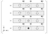
- Figure 14 shows an example of how magnetization is twisted in a domain wall that occurs between two magnetic domains.
- the domain wall DW occurs between the first magnetic domain MD1 and the second magnetic domain MD2.
- the magnetization is twisted from the first magnetic domain MD1 toward the second magnetic domain MD2.
- FIG. 14(a) shows a first example of magnetization twisting, where the magnetization is twisted in the +x direction relative to the magnetization of the first magnetic domain MD1 and the second magnetic domain MD2 at the domain wall DW.
- FIG. 14(b) shows a second example of magnetization twisting, where the magnetization is twisted in the -x direction relative to the magnetization of the first magnetic domain MD1 and the second magnetic domain MD2 at the domain wall DW.
- FIG. 14(c) shows a third example of magnetization twisting, where the magnetization is twisted in the +y direction relative to the magnetization of the first magnetic domain MD1 and the second magnetic domain MD2 at the domain wall DW.
- FIGS. 14(d) shows a fourth example of magnetization twisting, where the magnetization is twisted in the -y direction relative to the magnetization of the first magnetic domain MD1 and the second magnetic domain MD2 at the domain wall DW.
- the examples shown in FIGS. 14(a) and 14(b) are called Neel domain walls, and the examples shown in FIGS. 14(c) and 14(d) are called Bloch domain walls. Néel domain walls move when spin-orbit torque acts on them, but Bloch domain walls do not move when spin-orbit torque acts on them.
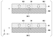
- FIG. 15 is a conceptual diagram of the Dzyaloshinskii-Moriya interaction acting between the nonmagnetic layer HM1 and the ferromagnetic layer M1.
- FIG. 15(a) is an example where the Dzyaloshinskii-Moriya interaction DMI1 acts in the +x direction
- FIG. 15(b) is an example where the Dzyaloshinskii-Moriya interaction DMI2 acts in the -x direction.
- the magnetization twist shown in the first example occurs.
- FIG. 15(a) when the Dzyaloshinskii-Moriya interaction DMI1 acts in the +x direction, the magnetization twist shown in the first example occurs.
- FIG. 15(a) when the Dzyaloshinskii-Moriya interaction DMI1 acts in the +x direction, the magnetization twist shown in the first example occurs.
- FIG. 15(a) when the Dzyaloshinskii-Moriya interaction DMI1 acts in the +x direction, the magnetization twist shown in the first example occurs
- the direction in which the Dzyaloshinskii-Moriya interaction acts is determined by the sign of the Dzyaloshinskii-Moriya interaction.
- the sign of the Dzyaloshinskii-Moriya interaction varies depending on the combination of the nonmagnetic layer HM1 and the ferromagnetic layer M1.
- the nonmagnetic layer 80 can be made of, for example, the same material as the second layer 15.
- the sign of the Dzyaloshinskii-Moriya interaction of the nonmagnetic layer 80 is the same as the sign of the Dzyaloshinskii-Moriya interaction of the second layer 15 of the spacer layer 13 that contacts the second ferromagnetic layer 12.
- the magnetization twist induced by the Dzyaloshinskii-Moriya interaction acting at the interface between the second layer 15 and the second ferromagnetic layer 12 and the magnetization twist induced by the Dzyaloshinskii-Moriya interaction acting at the interface between the nonmagnetic layer 80 and the second ferromagnetic layer 12 are opposite and cancel each other out.
- the magnetization in the domain wall DW is twisted in the +y or -y direction rather than in the x direction. In other words, the domain wall DW becomes a Bloch domain wall.
- the Bloch domain walls do not move even when spin-orbit torque acts on them. Therefore, when the above configuration is satisfied, the contribution of spin-orbit torque to the magnetization reversal of the second ferromagnetic layer 12 becomes smaller.
- the domain wall motion element 102 according to the third embodiment like the domain wall motion element 100 according to the first embodiment, has a small contribution of spin orbit torque to magnetization reversal and is highly reliable.
- FIG. 16 is an enlarged view of a characteristic portion of another example of the domain wall motion element according to the third embodiment.
- the sign of the Dzyaloshinskii-Moriya interaction of the nonmagnetic layer 81 may be the same as that of the Dzyaloshinskii-Moriya interaction of the first layer 14 of the spacer layer 13 that is in contact with the first ferromagnetic layer 11.
- This configuration also produces the same effect as the domain wall motion element 102 according to the third embodiment.
- Fig. 17 is a cross-sectional view of a domain wall motion element 104 according to the fourth embodiment.
- the domain wall motion element 104 shown in Fig. 17 differs from the domain wall motion element 100 in that the reference layer 30 is located farther from the substrate Sub than the stack 10.
- the domain wall motion element 104 is said to have a top pin structure.
- the domain wall motion element 100 has the reference layer 30 closer to the substrate Sub than the stack 10, and is said to have a bottom pin structure.
- the top pin structure shown in the domain wall motion element 104 also provides the same effects as the bottom pin structure.
- the spacer layer 13 is made up of two layers, the first layer 14 and the second layer 15, but the total number of non-magnetic layers constituting the spacer layer 13 is not limited to this example and may be three or more layers.
Landscapes
- Engineering & Computer Science (AREA)
- Computer Hardware Design (AREA)
- Hall/Mr Elements (AREA)
Abstract
この磁壁移動素子は、第1強磁性層と、第2強磁性層と、前記第1強磁性層と前記第2強磁性層とに挟まれるスペーサ層と、を備える、積層体を備える。前記第1強磁性層と前記第2強磁性層とのうち少なくとも一方は、内部に磁壁を有する。前記スペーサ層は、非磁性の第1層と、前記第1層に隣接する非磁性の第2層と、を有する。前記第1層は、負のスピンホール角を示し、前記第2層は、正のスピンホール角を示す。書き込み電流の一部は、前記スペーサ層の面内のいずれかの方向に沿って流れる。
Description
本発明は、磁壁移動素子及び磁気アレイに関する。
二つの強磁性層の磁化の相対角の変化に基づく抵抗値変化(磁気抵抗変化)を利用した磁気抵抗効果素子が知られている。例えば、特許文献1に記載の磁壁移動型の磁気抵抗効果素子(以下、磁壁移動素子という)は、磁気抵抗効果素子の一例である。磁壁移動素子は、磁壁の位置によって積層方向の抵抗値が変化し、多値又はアナログにデータを記録できる。
磁壁移動素子は、例えば特許文献2に記載のように、脳の機能を模倣したニューロモーフィックデバイスに利用することができる。
磁壁移動素子の磁壁は、強磁性層の磁化にトルクが加わり、強磁性層の磁化の一部が磁化反転することで移動する。スピントランスファートルク(STT)及びスピン軌道トルク(SOT)は、強磁性層の磁化に加わるトルクの一例である。スピントランスファートルクは、磁壁と交差する方向に電流が流れることで生じる。スピン軌道トルクは、磁壁を有する強磁性層に隣接する層からスピンが注入されることで生じる。スピン軌道トルクは、外部磁場、環境温度等の影響を受けやすく、環境によって特性が変化しやすい。そのため、磁化反転に対するスピン軌道トルクの寄与が大きいと、磁壁移動素子の特性が環境に応じて変動しやすくなる。環境変化に伴う磁壁移動素子の特性変化は、磁壁移動素子の信頼性を低下させる。
本開示は上記問題に鑑みてなされたものであり、スピン軌道トルクによる磁化反転の寄与を少なくした磁壁移動素子及び磁気アレイを提供することを目的とする。
第1の態様に係る磁壁移動素子は、積層体を備える。積層体は、第1強磁性層と、第2強磁性層と、前記第1強磁性層と前記第2強磁性層とに挟まれるスペーサ層と、を備える。前記第1強磁性層と前記第2強磁性層とのうち少なくとも一方は、内部に磁壁を有する。前記スペーサ層は、非磁性の第1層と、前記第1層に隣接する非磁性の第2層と、を有する。前記第1層は、負のスピンホール角を示し、前記第2層は、正のスピンホール角を示す。書き込み電流の一部は、前記スペーサ層の面内のいずれかの方向に沿って流れる。
以下、本実施形態について、図を適宜参照しながら詳細に説明する。以下の説明で用いる図面は、本発明の特徴をわかりやすくするために便宜上特徴となる部分を拡大して示している場合があり、各構成要素の寸法比率などは実際とは異なっていることがある。以下の説明において例示される材料、寸法等は一例であって、本発明はそれらに限定されるものではなく、本発明の効果を奏する範囲で適宜変更して実施することが可能である。
まず方向について定義する。x方向及びy方向は、後述する基板Sub(図3参照)の一面と略平行な方向である。x方向は、後述する積層体が延びる方向である。y方向は、x方向と直交する方向である。z方向は、後述する基板から磁壁移動素子へ向かう方向である。本明細書において、+z方向を「上」、-z方向を「下」として表す場合があるが、これら表現は便宜上のものであり、重力方向を規定するものではない。また本明細書で「x方向に延びる」とは、例えば、x方向、y方向、及びz方向の各寸法のうち最小の寸法よりもx方向の寸法が大きいことを意味する。他の方向に延びる場合も同様である。
[第1実施形態]
図1は、第1実施形態にかかる磁気アレイMAのブロック図である。磁気アレイMAは、集積領域1と周辺領域2とを有する。磁気アレイMAは、例えば、磁気メモリ、積和演算器、ニューロモーフィックデバイス、スピンメモリスタ、磁気光学素子に利用できる。
図1は、第1実施形態にかかる磁気アレイMAのブロック図である。磁気アレイMAは、集積領域1と周辺領域2とを有する。磁気アレイMAは、例えば、磁気メモリ、積和演算器、ニューロモーフィックデバイス、スピンメモリスタ、磁気光学素子に利用できる。
集積領域1は、複数の磁壁移動素子が集積された領域である。磁気アレイMAをメモリとして用いる場合は、集積領域1にデータが蓄積される。磁気アレイMAをニューロモーフィックデバイスとして用いる場合は、集積領域1で学習及び推論が行われる。
周辺領域2は、集積領域1内の磁壁移動素子の動作を制御する制御素子が実装されている領域である。周辺領域2は、例えば、パルス印加装置3、抵抗検出装置4、出力部5を有する。
パルス印加装置3は、集積領域1内の複数の磁壁移動素子の少なくとも一つにパルスを印加できるように構成されている。パルス印加装置3は、例えば、制御部6と電源7とを有する。
制御部6は、例えば、プロセッサとメモリとを有する。プロセッサは、例えば、CPU(Central Processing Unit)である。プロセッサは、メモリに記憶された動作プログラムに基づいて動作する。制御部6は、例えば、パルスを印加する磁壁移動素子のアドレス、所定の磁壁移動素子に印加するパルスの大きさ(電圧、パルス長)等を制御する。制御部6は、この他、クロック、カウンタ、乱数発生器等を有してもよい。クロックは、パルスを印加するタイミングの指標となり、カウンタは、パルスを印加した回数等をカウントする。電源7は、制御部6からの指示に従い、磁壁移動素子に向かってパルスを印加する。
抵抗検出装置4は、集積領域1内の磁壁移動素子の抵抗値を検出できるように構成されている。抵抗検出装置4は、集積領域1内の磁壁移動素子のそれぞれの抵抗を検出してもよいし、例えば同じ列に属する磁壁移動素子の抵抗の合計を検出してもよい。抵抗検出装置4は、例えば、検出した抵抗値の大きさを比較する比較器を有する。比較器は、例えば、検出した抵抗値同士を比較してもよいし、事前に設定された基準抵抗値と検出した抵抗値とを比較してもよい。
出力部5は、抵抗検出装置4に接続されている。出力部5は、例えば、プロセッサ、出力コンデンサ、増幅器、コンバータ等を有する。磁気アレイMAをニューロモーフィックデバイスとして用いる場合は、出力部5は、抵抗検出装置4の検出結果を活性化関数に代入する演算を行ってもよい。演算は、例えば、プロセッサで行われる。出力部5は、演算結果を外部に出力する。磁気アレイMAをニューロモーフィックデバイスとして用いる場合は、例えば、演算結果を他の磁気アレイの入力信号として出力する等の動作を行ってもよいし、識別率として外部に出力する等の動作を行ってもよい。また出力部5は、演算結果をパルス印加装置3にフィードバックしてもよい。
図2は、第1実施形態に係る集積領域1の回路図である。集積領域1は、複数の磁壁移動素子100と、複数の第1配線WLと、複数の第2配線CLと、複数の第3配線RLと、複数の第1スイッチング素子SW1と、複数の第2スイッチング素子SW2と、を備える。第3スイッチング素子SW3は、例えば、周辺領域2のパルス印加装置3に属してもよい。
複数の磁壁移動素子100は、例えば、行列状に配列する。複数の磁壁移動素子100は、実物の素子が行列状に配列するものに限られず、回路図において行列に配列するものでもよい。
第1配線WLのそれぞれは、書き込み配線である。第1配線WLはそれぞれ、パルス印加装置3と1つ以上の磁壁移動素子100とを電気的に接続する。第2配線CLのそれぞれは、データの書き込み時及び読み出し時の両方に用いることができる共通配線である。第2配線CLのそれぞれは、例えば、抵抗検出装置4に接続されている。第2配線CLは、複数の磁壁移動素子100のそれぞれに設けられてもよいし、複数の磁壁移動素子100に亘って設けられてもよい。第3配線RLのそれぞれは、読み出し配線である。第3配線RLはそれぞれ、パルス印加装置3と1つ以上の磁壁移動素子100とを電気的に接続する。
第1スイッチング素子SW1、第2スイッチング素子SW2及び第3スイッチング素子SW3は、電流の流れを制御する素子である。第1スイッチング素子SW1、第2スイッチング素子SW2及び第3スイッチング素子SW3は、例えば、トランジスタ、オボニック閾値スイッチ(OTS:Ovonic Threshold Switch)のように結晶層の相変化を利用した素子、金属絶縁体転移(MIT)スイッチのようにバンド構造の変化を利用した素子、ツェナーダイオード及びアバランシェダイオードのように降伏電圧を利用した素子、原子位置の変化に伴い伝導性が変化する素子である。
第1スイッチング素子SW1、第2スイッチング素子SW2は、例えば、それぞれの磁壁移動素子100に一つずつ接続されている。第1スイッチング素子SW1は、例えば、磁壁移動素子100と第1配線WLとの間に接続されている。第2スイッチング素子SW2は、例えば、磁壁移動素子100と第2配線CLとの間に接続されている。第3スイッチング素子SW3は、例えば、複数の磁壁移動素子100に亘って接続されている。第3スイッチング素子SW3は、例えば、第3配線RLに接続されている。
第1スイッチング素子SW1、第2スイッチング素子SW2及び第3スイッチング素子SW3の位置関係は、図2に示す場合に限られない。例えば、第1スイッチング素子SW1は、複数の磁壁移動素子100に亘って接続され、第1配線WLの上流に位置してもよい。また例えば、第2スイッチング素子SW2は、複数の磁壁移動素子100に亘って接続され、第2配線CLの上流に位置してもよい。また例えば、第3スイッチング素子SW3は、それぞれの磁壁移動素子100に一つずつ接続されていてもよい。
図3は、第1実施形態に係る集積領域1の磁壁移動素子100の近傍の断面図である。図3は、図2における一つの磁壁移動素子100を積層体10のy方向の幅の中心を通るxz平面で切断した断面である。
図3に示す第1スイッチング素子SW1及び第2スイッチング素子SW2は、トランジスタTrである。トランジスタTrは、ゲート電極Gと、ゲート絶縁膜GIと、基板Subに形成されたソースS及びドレインDと、を有する。ソースSとドレインDは、電流の流れ方向によって既定されるものであり、いずれも半導体の活性領域である。図3は一例を示しただけであり、ソースSとドレインDの位置関係は反転していてもよい。基板Subは、例えば、半導体基板である。第3スイッチング素子SW3は、第3配線RLと電気的に接続され、例えば、図3においてy方向にずれた位置にある。
トランジスタTr、第1配線WL、第2配線CL、第3配線RL及び磁壁移動素子100の間は、z方向に延びるビア配線Vw又はxy面内のいずれかの方向に延びる面内配線IPwで接続されている。ビア配線Vw及び面内配線IPwは、導電性を有する材料を含む。z方向の異なる階層間は、ビア配線Vwを除いて、絶縁層90が形成されている。
絶縁層90は、多層配線の配線間や素子間を絶縁する絶縁層である。磁壁移動素子100とトランジスタTrとは、ビア配線Vwを除いて、絶縁層90によって電気的に分離されている。絶縁層90は、例えば、酸化シリコン(SiOx)、窒化シリコン(SiNx)、炭化シリコン(SiC)、窒化クロム、炭窒化シリコン(SiCN)、酸窒化シリコン(SiON)、酸化アルミニウム(Al2O3)、酸化ジルコニウム(ZrOx)等である。
図4は、磁壁移動素子100を積層体10のy方向の中心を通るxz平面で切断した断面図である。図に示す矢印は、強磁性体の磁化の配向方向の一例である。図5は、磁壁移動素子100をz方向から見た平面図である。
磁壁移動素子100は、例えば、積層体10と非磁性層20と参照層30と磁化固定層40と磁化固定層50と電極60とを備える。集積領域1に含まれる複数の磁壁移動素子のうち少なくとも一つは、図4及び図5に示す磁壁移動素子100である。
積層体10は、z方向から見ると、x方向の長さがy方向の長さより長い。積層体10は、例えば、第1強磁性層11と第2強磁性層12とスペーサ層13とを備える。第1強磁性層11の磁化は、第2強磁性層12の磁化と磁気結合している。そのため、積層体10は、全体で一つの強磁性層とみなすこともできる。
積層体10は、2つの異なる磁区を有し、2つの磁区の境界に磁壁DWを有する。磁壁DWは、積層体10内部をx方向に移動する。積層体10は、磁気的な状態の変化により情報を磁気記録可能な層である。積層体10は、磁壁移動層、アナログ層、自由層、磁気記録層とも言われる。
積層体10は、第1領域A1と第2領域A2と第3領域A3を有する。積層体10は、x方向に、磁壁DWが移動可能な磁壁移動領域と、磁化が固定された磁化固定領域と、を含む。
第1領域A1は、磁化の配向方向が一方向に固定された領域である。第1領域A1は、磁化固定領域の一例である。磁化が固定されているとは、磁壁移動素子100の通常の動作(想定を超える外力が印加されていない)において、磁化が反転しないことをいう。第1領域A1は、例えば、積層体10のうちz方向からみて磁化固定層40と重なる領域である。第1領域A1の磁化は、例えば、磁化固定層40の磁化M40によって固定されている。
第2領域A2は、磁化の配向方向が一方向に固定された領域である。第2領域A2は、磁化固定領域の一例である。第2領域A2の磁化の配向方向は、第1領域A1の磁化の配向方向と異なる。第2領域A2の磁化の配向方向は、例えば、第1領域A1の磁化の配向方向と反対である。第2領域A2は、例えば、積層体10のうちz方向からみて磁化固定層50と重なる領域である。第2領域A2の磁化は、例えば、磁化固定層50の磁化M50によって固定されている。
第3領域A3は、積層体10の第1領域A1及び第2領域A2以外の領域である。第3領域A3は、例えば、x方向に第1領域A1と第2領域A2とに挟まれる領域である。
第3領域A3は、磁化の向きが変化し、磁壁DWが移動できる領域である。第3領域A3は、磁壁移動可能領域の一例である。第3領域A3は、第1磁区と第2磁区とを有する。第1磁区と第2磁区とは、磁化の配向方向が反対である。第1磁区と第2磁区との境界が磁壁DWである。磁化M11A、磁化M12A、磁化M11C、磁化M12Cは、例えば、第1磁区に属する。磁化M11B、磁化M12B、磁化M11D、磁化M12Dは、例えば、第2磁区に属する。磁壁DWは、原則、第3領域A3内を移動し、第1領域A1及び第2領域A2には侵入しない。
第3領域A3内における第1磁区と第2磁区との体積の比率が変化すると、磁壁DWが移動する。磁壁DWは、例えば、第3領域A3のx方向に書き込み電流を流すことで移動する。
第1強磁性層11及び第2強磁性層12は、磁性体を含む。第1強磁性層11は、例えば、第2強磁性層12より非磁性層20の近くにある。
第1強磁性層11と第2強磁性層12とのうち少なくとも一方は、内部に磁壁DWを有する。第1強磁性層11と第2強磁性層12とは、いずれも内部に磁壁DWを有してもよい。例えば、第1強磁性層11は、内部に磁壁DWを有し、磁壁DWが移動可能な磁壁移動領域と、磁化が固定された磁化固定領域と、を含んでもよい。また例えば、第2強磁性層12は、内部に磁壁DWを有し、磁壁DWが移動可能な磁壁移動領域と、磁化が固定された磁化固定領域と、を含んでもよい。上述のように、磁壁移動領域は、第3領域A3に属する部分であり、磁化固定領域は、第1領域A1又は第2領域A2に属する部分である。
第1強磁性層11の磁化は、第2強磁性層12の磁化と磁気結合している。第1強磁性層11は、第2強磁性層12の磁気状態を反映する。第1強磁性層11と第2強磁性層12とが強磁性カップリングする場合は、第1強磁性層11と第2強磁性層12とは磁気状態が同一になり、第1強磁性層11と第2強磁性層12とが反強磁性カップリングする場合は、第1強磁性層11と第2強磁性層12とは磁気状態が反対になる。
第1強磁性層11及び第2強磁性層12は、例えば、Co、Ni、Fe、Pt、Pd、Gd、Tb、Mn、Ge、Gaからなる群から選択される少なくとも一つの元素を有する。
第1強磁性層11と第2強磁性層12とは、構成材料が同じでもよいし、構成材料が異なってもよい。第1強磁性層11と第2強磁性層12とは求められる機能が異なるため、第1強磁性層11と第2強磁性層12とは、構成材料が異なることが好ましい。
第1強磁性層11は、参照層30と共に非磁性層20を挟む。磁壁移動素子100の磁気抵抗変化は、非磁性層20を挟む2つの強磁性層の磁化の相対角の変化することで生じる。第1強磁性層11は、第2強磁性層12より磁壁移動素子100のMR比に与える影響が大きい。そのため、第1強磁性層11は、磁壁移動素子100のMR比を高くすることができる材料が求められる。第1強磁性層11は、例えば、CoFeBである。
第2強磁性層12は、第1強磁性層11より磁壁移動素子100のMR比に与える影響が小さい。そのため、第2強磁性層12には、磁壁DWの移動を制御しやすい材料を選択できる。第2強磁性層12は、例えば、CoとNiの積層膜、CoとPtの積層膜、CoとPdの積層膜、MnGa系材料、GdCo系材料、TbCo系材料等である。MnGa系材料、GdCo系材料、TbCo系材料等のフェリ磁性体は飽和磁化が小さく、磁壁DWを移動するために必要な閾値電流が小さくなる。またCoとNiの積層膜、CoとPtの積層膜、CoとPdの積層膜は、保磁力が大きく、磁壁DWの移動速度が遅くなる。
第1強磁性層11の膜厚h11と第2強磁性層12の膜厚h12は、同じでも、異なってもよい。例えば、第2強磁性層12の膜厚h12は、第1強磁性層11の膜厚h11より厚くてもよい。スピン軌道トルクは、隣接する層との界面からスピンが注入されることで生じる。第2強磁性層12の膜厚h12が厚いと、第2強磁性層12の磁化反転におけるスピン軌道トルクの寄与が小さくなる。上記のように、第1強磁性層11に磁壁移動素子100のMR比を高くする材料を選択し、第2強磁性層12に磁壁DWの移動を制御しやすい材料を選択した場合、第2強磁性層12は、第1強磁性層11より磁壁DWの移動に与える影響が大きい。つまり、第2強磁性層12の膜厚h12が厚いと、磁壁DWの移動に対するスピン軌道トルクの寄与が小さくなる。
スペーサ層13は、第1強磁性層11と第2強磁性層12との間にある。スペーサ層13は、第1強磁性層11と第2強磁性層12とを磁気的にカップリングする。スペーサ層13は、磁気結合層、中間層とも呼ばれる。スペーサ層13は、非磁性体を含む。スペーサ層13の厚みは、例えば、2nm以下であり、好ましくは1nm以下である。
図6は、第1実施形態に係る磁壁移動素子の特徴部分の拡大図である。スペーサ層13は、例えば、第1層14と第2層15とを有する。第1層14と第2層15は、互いに隣接する。第1層14と第2層15は、いずれも非磁性層である。
第1層14は、負のスピンホール角を示し、第2層15は、正のスピンホール角を示す。第1層14と第2層15の位置関係は、逆転してもよい。第1層14と第2層15とは、スピンホール角の符号(極性)が異なる。「スピンホール角」は、スピンホール効果の強さの指標の一つであり、書き込み電流に対するスピン流の変換効率を示す。スピンホール角の符号(極性)は、値の正負を意味し、“+”又は“-”である。書き込み電流の一部は、少なくともスペーサ層13に沿って流れる。書き込み電流は、スペーサ層13の他に、第1強磁性層11及び第2強磁性層12にも流れる。書き込み電流は、第1強磁性層11、第2強磁性層12及びスペーサ層13に並列に流れる。
スピンホール効果は、電流を流した場合にスピン軌道相互作用に基づき、電流の流れる方向と直交する方向にスピン流が誘起される現象である。スピンホール効果は、運動(移動)する電荷(電子)が運動(移動)方向を曲げられる点で、通常のホール効果と共通する。通常のホール効果は、磁場中で運動する荷電粒子の運動方向がローレンツ力によって曲げられる。これに対し、スピンホール効果は磁場が存在しなくても、電子が移動するだけ(電流が流れるだけ)でスピンの移動方向が曲げられる。
例えば、第1層14に沿って書き込み電流が流れると、第1層14の第1面14Aには、例えば+y方向に配向したスピンspが偏在し、第2面14Bには、-y方向に配向したスピンspが偏在する。また例えば、第2層15に沿って書き込み電流が流れると、第2層15の第1面15Aには、例えば-y方向に配向したスピンspが偏在し、第2面15Bには、+y方向に配向したスピンspが偏在する。スピン流は、これらのスピンの偏在(スピン分極)を解消するように、z方向に生じる。スピンホール角の極性が異なると、第1面と第2面のそれぞれに偏在するスピンの正負が反転する。
第1層14と第2層15とは、スピンホール角の符号が異なる。そのため、スペーサ層13全体で考えた場合、第1層14で生じるスピン流と、第2層15で生じるスピン流とは互いに打ち消し合う。その結果、第1強磁性層11又は第2強磁性層12に注入されるスピンの量が減る。つまり、第1層14と第2層15のスピンホール角の符号が異なると、第1強磁性層11又は第2強磁性層12の磁化反転に対するスピン軌道トルクの寄与が少なくなる。
スピンホール角の符号は、層の電子状態によって決まるため、層を構成する材料、層の厚み、隣接する材料等で変化する。例えば、層を構成する材料は合金のような複数の元素が固溶することによって符号が変化することもあれば、酸化や窒化、炭化などの化合物化することによって極性が変化することもある。また、異なる材料を積層することによって巨視的に電子状態を変えることによって符号が変化することもある。更に、層の厚みによってスピンホール角の符号が変化する場合もある。
スペーサ層13は、例えば、Mg、Au、Al、Hf、Ta、W、Mo、Pt、Pd、Cu、Ru、Irからなる群から選択されるいずれかの原子を含む。
第1層14は、例えば、第3族、第4族、第5族及び第6族のいずれかに属する原子を含む。第1層14は、例えば、第3族、第4族、第5族及び第6族のいずれかに属する金属元素を主として含む。「主として」とは、これらの金属元素の含有率が50atm%以上であることを示す。スピンホール角の符号は、材料のみによって決定されるものではないが、第1層14がこれらの材料を含むと、第1層14は負のスピンホール角を示しやすくなる。第1層14は、例えば、Taである。
また第1層14は、酸素、窒素、炭素のいずれかを含んでもよい。第1層14は、例えば、第3族、第4族、第5族及び第6族のいずれかに属する金属の酸化物、窒化物、炭化物のいずれかでもよい。例えば、第1層14は、窒化タンタル(TaN)でもよい。
第2層15は、例えば、第8族、第9族、第10族、第11族及び第12族のいずれかに属する原子を含む。第2層15は、例えば、第8族、第9族、第10族、第11族及び第12族のいずれかに属する原子を主として含む。スピンホール角の符号は、材料のみによって決定されるものではないが、第2層15がこれらの材料を含むと、第2層15は正のスピンホール角を示しやすくなる。第2層15は、例えば、Ptである。
また第2層15は、酸素、窒素、炭素のいずれかを含んでもよい。第2層15は、例えば、第8族、第9族、第10族、第11族及び第12族のいずれかに属する金属の酸化物、窒化物、炭化物のいずれかでもよい。
第1層14の膜厚は、第2層15の膜厚と同じでも異なってもよい。図7は、第1実施形態に係る磁壁移動素子の特徴部分の別の例の拡大図である。図7に示す第2層15の膜厚h15は、第1層14の膜厚h14より厚い。
例えば、第1層14と第2層15とのうちスピンホール角の絶対値が大きい方の層の膜厚は、第1層14と第2層15とのうちスピンホール角の絶対値が小さい方の層の膜厚より薄いことが好ましい。例えば、図7に示す第2層15は、第1層14よりスピンホール角の絶対値が小さい。スピンホール角の絶対値が大きいほど、スピンホール効果は強く生じる。スピンホール角の絶対値と、第1層14及び第2層15の膜厚との関係が上記関係を満たすと、それぞれの層で生じたスピン流同士が打ち消し合い、スペーサ層13内で実効的に生じるスピン流を低減できる。
また例えば、第1層14と第2層15とのうち抵抗率が大きい方の層の膜厚は、第1層14と第2層15とのうち抵抗率が小さい方の層の膜厚の膜厚より厚いことが好ましい。例えば、図7に示す第2層15は、第1層14より抵抗率が大きい。第1層14及び第2層15の膜厚と抵抗率との関係が上記関係を満たすと、書き込み電流の第1層14と第2層とに対する分流比が同程度となり、スペーサ層13内で実効的に生じるスピン流を低減できる。
第1層14及び第2層15のそれぞれの膜厚は、例えば、0.1nm以上20nm以下である。
非磁性層20は、積層体10と参照層30とに挟まれる。非磁性層20は、参照層30の一面に積層される。
非磁性層20は、例えば、非磁性の絶縁体、半導体又は金属からなる。非磁性層20は、例えば、非磁性の絶縁体であることが好ましい。非磁性の絶縁体は、例えば、Al2O3、SiO2、MgO、MgAl2O4、およびこれらのAl、Si、Mgの一部がZn、Be等に置換された材料である。これらの材料は、バンドギャップが大きく、絶縁性に優れる。非磁性の絶縁体は、例えば、Mg又はAlを含む酸化物である。非磁性層20が非磁性の絶縁体からなる場合、非磁性層20はトンネルバリア層である。非磁性の金属は、例えば、Cu、Au、Ag等である。非磁性の半導体は、例えば、Si、Ge、CuInSe2、CuGaSe2、Cu(In,Ga)Se2等である。
非磁性層20の厚みは、例えば、20Å以上であり、25Å以上でもよい。
参照層30は、積層体10と共に、非磁性層20を挟む。参照層30は、少なくとも一部が第3領域A3とz方向に重なる位置にある。参照層30は、例えば、積層体10より基板Subの近くにある。
参照層30の磁化は、積層体10の第3領域A3の磁化より反転しにくい。参照層30の磁化は、第3領域A3の磁化が反転する程度の外力が印加された際に向きが変化せず、固定されている。参照層30は、固定層と言われる場合もある。
参照層30は、強磁性体を含む。参照層30は、例えば、積層体10との間で、コヒーレントトンネル効果を得やすい材料を含む。参照層30は、例えば、Cr、Mn、Co、Fe及びNiからなる群から選択される金属、これらの金属を1種以上含む合金、これらの金属とB、C、及びNの少なくとも1種以上の元素とが含まれる合金等を含む。参照層30は、例えば、Co-Fe、Co-Fe-B、Ni-Feである。
参照層30は、例えば、ホイスラー合金でもよい。ホイスラー合金はハーフメタルであり、高いスピン分極率を有する。ホイスラー合金は、XYZ又はX2YZの化学組成をもつ金属間化合物であり、Xは周期表上でCo、Fe、Ni、あるいはCu族の遷移金属元素または貴金属元素であり、YはMn、V、CrあるいはTi族の遷移金属又はXの元素種であり、ZはIII族からV族の典型元素である。ホイスラー合金として例えば、Co2FeSi、Co2FeGe、Co2FeGa、Co2MnSi、Co2Mn1-aFeaAlbSi1-b、Co2FeGe1-cGac等が挙げられる。
参照層30及び非磁性層20のそれぞれは、例えば、x方向において、第3領域A3より長い。非磁性層20を挟んで参照層30と第3領域A3とが向き合う部分が、磁壁移動素子100の抵抗変化を担う。参照層30及び非磁性層20のx方向の長さが第3領域のx方向の長さより長いと、磁壁移動素子100の抵抗変化幅をより多値に区分しやすくなる。
参照層30は、例えば、x方向において、積層体10より長い。z方向から見て参照層30が積層体10の全体と重畳すると、積層体10の放熱性が向上する。その結果、第1領域A1の磁化及び第2領域A2の磁化の安定性が高まり、磁壁移動素子100のデータの信頼性が高まる。
磁化固定層40は、積層体10に接続されている。磁化固定層40は、積層体10の第1領域A1に接続されている。磁化固定層40の磁化M40は第1領域A1の磁化を固定する。磁化固定層40は、磁壁移動素子100に書き込み電流を印加する際に用いられる書き込み電極である。書き込み電流は、磁化固定層40と磁化固定層50との間に流れる。
磁化固定層40は、例えば、強磁性体である。磁化固定層40は、例えば、第1強磁性層11、第2強磁性層12又は参照層30と同様の材料を適用できる。また磁化固定層40は、複数の層を有し、シンセティック反強磁性構造(SAF構造)でもよい。
シンセティック反強磁性構造は、非磁性のスペーサ層を挟む二つの磁性層からなる。磁性層は、例えば、強磁性体を含み、IrMn、PtMn等の反強磁性体を含んでもよい。スペーサ層は、例えば、Ru、Ir、Rhからなる群から選択される少なくとも一つを含む。
また磁化固定層40は、強磁性体に限られない。磁化固定層40が強磁性体ではない場合は、磁化固定層40と重なる領域で積層体10を流れる電流の電流密度が急激に変化することで、磁壁DWの移動が制限され、第1領域A1の磁化が固定される。
磁化固定層50は、磁化固定層40と異なる位置で、積層体10に接続されている。磁化固定層50は、積層体10の第2領域A2に接続されている。磁化固定層50の磁化M50は第2領域A2の磁化を固定する。磁化固定層50は、磁壁移動素子100に書き込み電流を印加する際、及び、磁壁移動素子100に読出し電流を印加する際に用いられる共通電極である。
磁化固定層50は、磁化固定層40と同様の材料を用いることができる。磁化固定層50は、シンセティック反強磁性構造(SAF構造)でもよい。
磁化固定層50の膜厚は、磁化固定層40の膜厚より厚くてもよい。磁化固定層50の膜厚と磁化固定層40の膜厚とが異なると、磁化固定層50と磁化固定層40の保磁力に差が生じやすい。磁化固定層50と磁化固定層40の保磁力に差があると、製造時点で、磁化固定層50の磁化M50の配向方向と磁化固定層40の磁化M40の配向方向とを異なる方向に設定しやすくなる。
磁化固定層40及び磁化固定層50の形状は特に問わない。図5では、z方向から見た磁化固定層40及び磁化固定層50の平面視形状が矩形の例を示したが、図8に示すように磁化固定層40及び磁化固定層50の平面視形状は円形でもよい。図8は、第1実施形態に係る磁壁移動素子100の別の例の平面図である。磁化固定層40及び磁化固定層50の平面視形状は、例えば、矩形、円形、楕円形等である。
電極60は、参照層30に接続されている。電極60は、磁壁移動素子100に読出し電流を印加する際に用いられる読出し電極である。読出し電流は、例えば、磁化固定層50と電極60との間に流れる。電極60は、導電性を有する材料を含む。電極60は、z方向に延びるビア配線でもよい。
磁壁移動素子100は、積層体10、非磁性層20及び参照層30以外の層を有してもよい。例えば、参照層30の非磁性層20と反対側の面に、スペーサ層を介して、磁性層を設けてもよい。参照層30、スペーサ層、磁性層は、シンセティック反強磁性構造(SAF構造)となる。また、磁性層のスペーサ層と反対側の面に、下地層を設けてもよい。
磁壁移動素子100の各層の磁化の向きは、例えば磁化曲線を測定することにより確認できる。磁化曲線は、例えば、MOKE(Magneto Optical Kerr Effect)を用いて測定できる。MOKEによる測定は、直線偏光を測定対象物に入射させ、その偏光方向の回転等が起こる磁気光学効果(磁気Kerr効果)を用いることにより行う測定方法である。
磁壁移動素子100は、各層の積層工程と、各層の一部を所定の形状に加工する加工工程により形成される。各層の積層は、スパッタリング法、化学気相成長(CVD)法、電子ビーム蒸着法(EB蒸着法)、原子レーザデポジッション法等を用いることができる。各層の加工は、フォトリソグラフィーおよびエッチング(例えば、Arエッチング)等を用いて行うことができる。
次いで、磁気アレイMAへの信号の書き込み動作及び磁気アレイMAからの信号の読出し動作を説明する。
まず磁気アレイMAへの信号の書き込み動作について説明する。書き込み動作は、例えば、制御部6に格納された動作プログラムをプロセッサが実行することで行われる。
まずパルス印加装置3は、動作プログラムに従い、パルスを印加する磁壁移動素子100を選択する。磁気アレイMAを磁気メモリとして用いる場合、パルスを印加する磁壁移動素子100は、データを記憶させる素子である。磁気アレイMAをニューラルネットワークとして用いる場合、パルスを印加する磁壁移動素子100は、学習に応じて重みを変化させる素子である。
複数の磁壁移動素子100のうち何れの磁壁移動素子100に対してパルスを印加するかは、制御部6が制御する。制御部6は、パルスを印加する磁壁移動素子100に接続された第1スイッチング素子SW1及び第2スイッチング素子SW2をONにし、第3スイッチング素子SW3をOFFにする。またパルスを印加しない磁壁移動素子100に接続された第1スイッチング素子SW1及び第2スイッチング素子SW2の少なくともいずれか一方をOFFにする。
そして、パルス印加装置3は、動作プログラムに従い、磁壁移動素子100に向かって書き込みパルスを出力する。書き込みパルスは、磁壁移動素子100の積層体10に沿って、磁化固定層40と磁化固定層50との間に印加される。その結果、書き込み電流の一部は、スペーサ層13の面内のいずれかの方向に沿って流れる。図4及び図6で示す例において、書き込み電流の一部は、スペーサ層13の面内に沿ってx方向に流れる。書き込みパルスは、矩形波でも、スパイク波でも、その他の波形の波でもよい。書き込みパルスの回数、大きさ等を変えることで、磁壁DWの位置が変化し、特定の磁壁移動素子100に信号が書き込まれる。
次いで、磁気アレイMAからの信号の読出し動作について説明する。読出し動作は、例えば、制御部6に格納された動作プログラムをプロセッサが実行することで行われる。
まずパルス印加装置3は、動作プログラムに従い、読出しパルスを印加する磁壁移動素子100を選択する。磁気アレイMAを磁気メモリとして用いる場合、読出しパルスを印加する磁壁移動素子100は、データを読み出す素子である。磁気アレイMAをニューラルネットワークとして用いる場合、所定の磁壁移動素子100への読出しパルスの印加は、入力と重みとの積演算に対応する。すなわち、磁気アレイMAをニューラルネットワークとして用いる場合、読出し動作は、ニューラルネットワークの識別演算である。
複数の磁壁移動素子100のうち何れの磁壁移動素子100に対してパルスを印加するかは、制御部6が制御する。制御部6は、パルスを印加する磁壁移動素子100に接続された第3スイッチング素子SW3及び第2スイッチング素子SW2をONにし、第1スイッチング素子SW1をOFFにする。またパルスを印加しない磁壁移動素子100に接続された第3スイッチング素子SW3及び第2スイッチング素子SW2の少なくともいずれか一方をOFFにする。
次いで、パルス印加装置3は、動作プログラムに従い、所定の磁壁移動素子100に読出しパルスを印加する。読出しパルスは、例えば、電極60と磁化固定層50との間に印加される。読出しパルスの電圧は、積層体10の磁壁DWを動かすのに必要な臨界電流密度未満の電流密度が得られる電圧である。すなわち、読出しパルスは、磁壁DWを動かさない。
抵抗検出装置4は、読出しパルスが印加された磁壁移動素子100の抵抗値を検出する。出力部5は、例えば、演算結果を外部に出力する。このような手順で、特定の磁壁移動素子100から信号を読み出すことができる。
本実施形態に係る磁壁移動素子100は、積層体10のスペーサ層13がスピンホール角の符号の異なる第1層14と第2層15とを含む。磁壁移動素子100の書き込み電流の一部は、スペーサ層13に沿って流れる。スペーサ層13全体で考えた場合、第1層14で生じるスピン流と、第2層15で生じるスピン流とは互いに打ち消し合う。その結果、第1強磁性層11又は第2強磁性層12に実効的に注入されるスピンの量が減る。つまり、第1層14と第2層15のスピンホール角の符号が異なると、第1強磁性層11又は第2強磁性層12の磁化反転に対するスピン軌道トルクの寄与が少なくなる。磁壁移動が主にスピン軌道トルクによって生じる場合、磁壁移動の特性が外部磁場、環境温度等の影響を受けやすい。本実施形態に係る磁壁移動素子100は、磁化反転に対するスピン軌道トルクの寄与が小さく、信頼性が高い。
[第2実施形態]
図9は、第2実施形態に係る磁壁移動素子101を積層体10のy方向の中心を通るxz平面で切断した断面図である。図に示す矢印は、強磁性体の磁化の配向方向の一例である。磁壁移動素子101の平面視形状は、磁壁移動素子100と同様である。
図9は、第2実施形態に係る磁壁移動素子101を積層体10のy方向の中心を通るxz平面で切断した断面図である。図に示す矢印は、強磁性体の磁化の配向方向の一例である。磁壁移動素子101の平面視形状は、磁壁移動素子100と同様である。
磁壁移動素子101は、非磁性層70をさらに有する点が、磁壁移動素子100と異なる。磁壁移動素子101において、磁壁移動素子100と同様の構成については、同様の符号を付し、説明を省く。
非磁性層70は、第2強磁性層12のスペーサ層13から遠い側の面に接する。非磁性層70は、第2強磁性層12のスペーサ層13と接する面と反対側の面に接する。
図10は、第2実施形態に係る磁壁移動素子101の特徴部分の拡大図である。非磁性層70のスピンホール角の符号は、スペーサ層13のうち第2強磁性層12と接する第2層15の符号と同じである。すなわち、非磁性層70のスピンホール角の符号は、第2層15のスピンホール角の符号と同じである。第2層15は、スペーサ層13のうち、非磁性層70と接する第2強磁性層12と、接する層である。非磁性層70には、第2層15と同様の材料を用いることができる。
非磁性層70と第2層15のスピンホール角の符号が同じであると、非磁性層70から第2強磁性層12に注入されるスピンの向きと、第2層15から第2強磁性層12に注入されるスピンの向きとが反対になる。第2強磁性層12に注入されるスピン同士は互いに打ち消し合うため、実効的に第2強磁性層12に注入されるスピン量が減る。その結果、第2強磁性層12の磁化反転に対するスピン軌道トルクの寄与がより少なくなる。
第2実施形態に係る磁壁移動素子101は、第1実施形態に係る磁壁移動素子100と同様に、磁化反転に対するスピン軌道トルクの寄与が小さく、信頼性が高い。
ここでは一例として、非磁性層70が第2強磁性層12に接する例を示した。一方で、非磁性層は第1強磁性層11と接してもよい。図11は、第2実施形態に係る磁壁移動素子の別の例の特徴部分の拡大図である。図11に示す磁壁移動素子は、非磁性層71を有する点が、磁壁移動素子100と異なる。非磁性層71は、第1強磁性層11のスペーサ層13と接する面と反対側の面に接する。
非磁性層71のスピンホール角の符号は、スペーサ層13のうち第1強磁性層11と接する第1層14の符号と同じである。すなわち、非磁性層71のスピンホール角の符号は、第1層14のスピンホール角の符号と同じである。第1層14は、スペーサ層13のうち、非磁性層71と接する第1強磁性層11と、接する層である。非磁性層71には、第1層14と同様の材料を用いることができる。
非磁性層71と第1層14のスピンホール角の符号が同じであると、非磁性層71から第1強磁性層11に注入されるスピンの向きと、第1層14から第1強磁性層11に注入されるスピンの向きとが反対になる。第1強磁性層11に注入されるスピン同士は互いに打ち消し合うため、実効的に第1強磁性層11に注入されるスピン量が減る。その結果、第1強磁性層11の磁化反転に対するスピン軌道トルクの寄与がより少なくなる。したがって、当該構成は、第1実施形態に係る磁壁移動素子100と同様の効果を奏する。
[第3実施形態]
図12は、第3実施形態に係る磁壁移動素子102を積層体10のy方向の中心を通るxz平面で切断した断面図である。図に示す矢印は、強磁性体の磁化の配向方向の一例である。磁壁移動素子102の平面視形状は、磁壁移動素子100と同様である。
図12は、第3実施形態に係る磁壁移動素子102を積層体10のy方向の中心を通るxz平面で切断した断面図である。図に示す矢印は、強磁性体の磁化の配向方向の一例である。磁壁移動素子102の平面視形状は、磁壁移動素子100と同様である。
磁壁移動素子102は、非磁性層80をさらに有する点が、磁壁移動素子100と異なる。磁壁移動素子102において、磁壁移動素子100と同様の構成については、同様の符号を付し、説明を省く。
非磁性層80は、第2強磁性層12のスペーサ層13から遠い側の面に接する。非磁性層80は、第2強磁性層12のスペーサ層13と接する面と反対側の面に接する。
図13は、第3実施形態に係る磁壁移動素子102の特徴部分の拡大図である。非磁性層80と第2強磁性層12との間に働くジャロシンスキー・守谷相互作用の符号は、第2層15と第2強磁性層12との間に働くジャロシンスキー・守谷相互作用の符号と同じである。第2層15は、スペーサ層13のうち第2強磁性層12と接する層である。ジャロシンスキー・守谷相互作用は、磁性体と非磁性体との界面において生じるスピンの捻れを誘起する相互作用である。またジャロシンスキー・守谷相互作用の符号は、値の正負であり、“+”又は“-”である。ジャロシンスキー・守谷相互作用の符号が異なると、磁化に作用する力の向きが反対になる。
図14は、二つの磁区の間に生じる磁壁における磁化の捻れ方の例を示す。磁壁DWは、第1磁区MD1と第2磁区MD2の間に生じる。磁壁DWでは、第1磁区MD1から第2磁区MD2に向かって磁化が捻れている。
図14(a)は磁化の捻れ方の第1例を示し、磁化は磁壁DWにおいて第1磁区MD1及び第2磁区MD2の磁化に対して+x方向に捻れている。図14(b)は磁化の捻れ方の第2例を示し、磁化は磁壁DWにおいて第1磁区MD1及び第2磁区MD2の磁化に対して-x方向に捻れている。図14(c)は磁化の捻れ方の第3例を示し、磁化は磁壁DWにおいて第1磁区MD1及び第2磁区MD2の磁化に対して+y方向に捻れている。図14(d)は磁化の捻れ方の第4例を示し、磁化は磁壁DWにおいて第1磁区MD1及び第2磁区MD2の磁化に対して-y方向に捻れている。図14(a)及び図14(b)に示す例はネール磁壁と言われ、図14(c)及び図14(d)に示す例はブロッホ磁壁と言われる。ネール磁壁はスピン軌道トルクが作用することで動くが、ブロッホ磁壁はスピン軌道トルクが作用しても動かない。
図15は、非磁性層HM1と強磁性層M1との間に作用するジャロシンスキー・守谷相互作用の概念図である。図15(a)は、+x方向にジャロシンスキー・守谷相互作用DMI1が作用する例であり、図15(b)は、-x方向にジャロシンスキー・守谷相互作用DMI2が作用する例である。図15(a)に示すように、+x方向にジャロシンスキー・守谷相互作用DMI1が作用すると、第1例で示す磁化の捻れが生じる。図15(b)に示すように、-x方向にジャロシンスキー・守谷相互作用DMI2が作用すると、第2例で示す磁化の捻れが生じる。すなわち、ジャロシンスキー・守谷相互作用が働くことでネール磁壁が形成される。
ジャロシンスキー・守谷相互作用がいずれの方向に作用するかは、ジャロシンスキー・守谷相互作用の符号によって決まる。ジャロシンスキー・守谷相互作用の符号は、非磁性層HM1と強磁性層M1との組み合わせによって変わる。非磁性層80には、例えば、第2層15と同様の材料を用いることができる。
非磁性層80のジャロシンスキー・守谷相互作用の符号は、スペーサ層13のうち第2強磁性層12と接する第2層15のジャロシンスキー・守谷相互作用の符号と同じである。この場合、図13に示すように、第2層15と第2強磁性層12との界面で作用するジャロシンスキー・守谷相互作用が誘起する磁化の捻れと、非磁性層80と第2強磁性層12との界面で作用するジャロシンスキー・守谷相互作用が誘起する磁化の捻れが、反対になり、互いに打ち消し合う。その結果、磁壁DWにおける磁化はx方向に捻れずに、+y方向又は-y方向に捻れる。すなわち、磁壁DWはブロッホ磁壁となる。
上述のように、ブロッホ磁壁はスピン軌道トルクが作用しても動かない。そのため、上記の構成を満たすと、第2強磁性層12の磁化反転に対するスピン軌道トルクの寄与がより少なくなる。
第3実施形態に係る磁壁移動素子102は、第1実施形態に係る磁壁移動素子100と同様に、磁化反転に対するスピン軌道トルクの寄与が小さく、信頼性が高い。
また第3実施形態においても第2実施形態と同様に、非磁性層81が第1強磁性層11と接してもよい。図16は、第3実施形態に係る磁壁移動素子の別の例の特徴部分の拡大図である。非磁性層81のジャロシンスキー・守谷相互作用の符号は、スペーサ層13のうち第1強磁性層11と接する第1層14のジャロシンスキー・守谷相互作用と同じでもよい。当該構成においても、第3実施形態に係る磁壁移動素子102と同様の効果を奏する。
[第4実施形態]
図17は、第4実施形態に係る磁壁移動素子104の断面図である。図17に示す磁壁移動素子104は、参照層30が積層体10より基板Subから離れた位置にある点が、磁壁移動素子100と異なる。磁壁移動素子104は、トップピン構造と言われる。磁壁移動素子100は、参照層30が積層体10より基板Subの近くにあり、ボトムピン構造と言われる。磁壁移動素子104に示すようなトップピン構造においても、ボトムピン構造の場合と同様の効果が得られる。
図17は、第4実施形態に係る磁壁移動素子104の断面図である。図17に示す磁壁移動素子104は、参照層30が積層体10より基板Subから離れた位置にある点が、磁壁移動素子100と異なる。磁壁移動素子104は、トップピン構造と言われる。磁壁移動素子100は、参照層30が積層体10より基板Subの近くにあり、ボトムピン構造と言われる。磁壁移動素子104に示すようなトップピン構造においても、ボトムピン構造の場合と同様の効果が得られる。
以上、本発明の好ましい実施の形態について詳述したが、本発明はこれらの実施形態に限られるものではない。例えば、それぞれの実施形態の特徴的な構成を組み合わせてもよいし、発明の要旨を変更しない範囲で一部を変更してもよい。
例えば、第1実施形態から第4実施形態では、スペーサ層13が第1層14と第2層15の2層からなる例を示したが、スペーサ層13を構成する非磁性層の総数はこの例に限られず、3層以上でもよい。
1…集積領域、2…周辺領域、3…パルス印加装置、4…抵抗検出装置、5…出力部、6…制御部、7…電源、10…積層体、11…第1強磁性層、12…第2強磁性層、13…スペーサ層、14…第1層、15…第2層、20…非磁性層、30…参照層、40,50…磁化固定層、60…電極、70,71,80,81…非磁性層、90…絶縁層、100,101,102,103…磁壁移動素子、A1…第1領域、A2…第2領域、A3…第3領域、WL…第1配線、CL…第2配線、RL…第3配線、DW…磁壁、MA…磁気アレイ
Claims (12)
- 第1強磁性層と、第2強磁性層と、前記第1強磁性層と前記第2強磁性層に挟まれるスペーサ層と、を備える、積層体を備え、
前記第1強磁性層と前記第2強磁性層とのうち少なくとも一方は、内部に磁壁を有し、
前記スペーサ層は、非磁性の第1層と、前記第1層に隣接する非磁性の第2層と、を有し、
前記第1層は、負のスピンホール角を示し、
前記第2層は、正のスピンホール角を示し、
書き込み電流の一部は、前記スペーサ層の面内のいずれかの方向に沿って流れる、磁壁移動素子。 - 前記第1層と前記第2層とのうちスピンホール角の絶対値が大きい方の層の膜厚は、前記第1層と前記第2層とのうちスピンホール角の絶対値が小さい方の層の膜厚より薄い、請求項1に記載の磁壁移動素子。
- 前記第1層と前記第2層とのうち抵抗率が大きい方の層の膜厚は、前記第1層と前記第2層とのうち抵抗率が小さい方の層の膜厚より厚い、請求項1に記載の磁壁移動素子。
- 前記スペーサ層は、Mg、Au、Al、Hf、Ta、W、Mo、Pt、Pd、Cu、Ru、Irからなる群から選択されるいずれかの原子を含む、請求項1に記載の磁壁移動素子。
- 前記第1層は、第3族、第4族、第5族及び第6族のいずれかに属する原子を含み、
前記第2層は、第8族、第9族、第10族、第11族及び第12族のいずれかに属する原子を含む、請求項4に記載の磁壁移動素子。 - 前記第1強磁性層と前記第2強磁性層とは、構成材料が異なる、請求項1に記載の磁壁移動素子。
- 前記第1強磁性層は、内部に磁壁を有し、
前記第1強磁性層は、面内の異なる位置に、磁壁が移動できる磁壁移動可能領域と、磁化が固定された磁化固定領域とを有する、請求項1に記載の磁壁移動素子。 - 非磁性層をさらに備え、
前記非磁性層は、前記第1強磁性層の前記スペーサ層から遠い側の面、又は、前記第2強磁性層の前記スペーサ層から遠い側の面に接し、
前記非磁性層のスピンホール角の符号は、前記スペーサ層のうち、前記非磁性層と接する第1強磁性層又は第2強磁性層と、接する層のスピンホール角の符号と同じである、請求項1に記載の磁壁移動素子。 - 非磁性層をさらに備え、
前記非磁性層は、前記第1強磁性層の前記スペーサ層から遠い側の面、又は、前記第2強磁性層の前記スペーサ層から遠い側の面に接し、
前記非磁性層のジャロシンスキー・守谷相互作用の符号は、前記スペーサ層のうち、前記非磁性層と接する第1強磁性層又は第2強磁性層と、接する層のジャロシンスキー・守谷相互作用の符号と同じである、請求項1に記載の磁壁移動素子。 - 非磁性層をさらに備え、
前記非磁性層は、Mg又はAlを含む酸化物を含み、前記第2強磁性層より前記第1強磁性層の近くにあり、
前記第2強磁性層の膜厚は、前記第1強磁性層の膜厚より厚い、請求項1に記載の磁壁移動素子。 - 非磁性層と参照層とをさらに備え、
前記非磁性層は、前記積層体と前記参照層との間にあり、
前記参照層は、磁化が固定された強磁性体を含む、請求項1に記載の磁壁移動素子。 - 請求項1に記載の磁壁移動素子を含む、磁気アレイ。
Priority Applications (1)
| Application Number | Priority Date | Filing Date | Title |
|---|---|---|---|
| PCT/JP2023/005968 WO2024176297A1 (ja) | 2023-02-20 | 2023-02-20 | 磁壁移動素子及び磁気アレイ |
Applications Claiming Priority (1)
| Application Number | Priority Date | Filing Date | Title |
|---|---|---|---|
| PCT/JP2023/005968 WO2024176297A1 (ja) | 2023-02-20 | 2023-02-20 | 磁壁移動素子及び磁気アレイ |
Publications (1)
| Publication Number | Publication Date |
|---|---|
| WO2024176297A1 true WO2024176297A1 (ja) | 2024-08-29 |
Family
ID=92500426
Family Applications (1)
| Application Number | Title | Priority Date | Filing Date |
|---|---|---|---|
| PCT/JP2023/005968 Ceased WO2024176297A1 (ja) | 2023-02-20 | 2023-02-20 | 磁壁移動素子及び磁気アレイ |
Country Status (1)
| Country | Link |
|---|---|
| WO (1) | WO2024176297A1 (ja) |
Citations (4)
| Publication number | Priority date | Publication date | Assignee | Title |
|---|---|---|---|---|
| JP2018157108A (ja) * | 2017-03-17 | 2018-10-04 | 株式会社東芝 | 磁気メモリ |
| WO2019203132A1 (ja) * | 2018-04-18 | 2019-10-24 | 国立大学法人東北大学 | 磁気抵抗効果素子、磁気メモリ装置並びに磁気メモリ装置の書き込み及び読み出し方法 |
| WO2021006219A1 (ja) * | 2019-07-05 | 2021-01-14 | Tdk株式会社 | 磁気素子及び磁気記録アレイ |
| JP2022059565A (ja) * | 2020-10-01 | 2022-04-13 | Tdk株式会社 | 磁壁移動素子および磁気アレイ |
-
2023
- 2023-02-20 WO PCT/JP2023/005968 patent/WO2024176297A1/ja not_active Ceased
Patent Citations (4)
| Publication number | Priority date | Publication date | Assignee | Title |
|---|---|---|---|---|
| JP2018157108A (ja) * | 2017-03-17 | 2018-10-04 | 株式会社東芝 | 磁気メモリ |
| WO2019203132A1 (ja) * | 2018-04-18 | 2019-10-24 | 国立大学法人東北大学 | 磁気抵抗効果素子、磁気メモリ装置並びに磁気メモリ装置の書き込み及び読み出し方法 |
| WO2021006219A1 (ja) * | 2019-07-05 | 2021-01-14 | Tdk株式会社 | 磁気素子及び磁気記録アレイ |
| JP2022059565A (ja) * | 2020-10-01 | 2022-04-13 | Tdk株式会社 | 磁壁移動素子および磁気アレイ |
Similar Documents
| Publication | Publication Date | Title |
|---|---|---|
| JP7670581B2 (ja) | 磁壁移動素子および磁気アレイ | |
| JP7173311B2 (ja) | 磁壁移動素子、磁気記録アレイ及び半導体装置 | |
| CN112599660B (zh) | 磁畴壁移动元件和磁记录阵列 | |
| JP7624351B2 (ja) | 磁壁移動素子及び磁気アレイ | |
| JP7211564B1 (ja) | 磁壁移動素子、磁気アレイ及び磁壁移動素子の製造方法 | |
| JP7520673B2 (ja) | 集積装置及びニューロモーフィックデバイス | |
| CN113939913B (zh) | 磁记录阵列、神经形态器件及磁记录阵列的控制方法 | |
| JP7140294B2 (ja) | 磁気記録アレイ及びリザボア素子 | |
| JP2021132110A (ja) | 磁壁移動素子および磁気記録アレイ | |
| US20250126806A1 (en) | Domain wall motion element and magnetic array | |
| JP7802151B2 (ja) | ニューロモーフィックデバイス | |
| JP7470599B2 (ja) | 配線層、磁壁移動素子および磁気アレイ | |
| US20240420785A1 (en) | Magnetic domain wall motion element, magnetic recording array, and magnetic memory | |
| US12477953B2 (en) | Domain wall movement element, magnetoresistive element, and magnetic array | |
| WO2024189676A1 (ja) | 磁壁移動素子及び磁気アレイ | |
| JP7751723B2 (ja) | 磁気アレイ、磁気アレイの制御方法及び磁気アレイの動作プログラム | |
| US12457909B2 (en) | Magnetic domain wall moving element, magnetic array, and neuromorphic device | |
| JP7512116B2 (ja) | 磁気メモリ | |
| CN115458678B (zh) | 磁畴壁移动元件和磁阵列 | |
| CN113614920B (zh) | 磁记录阵列 | |
| JP7608291B2 (ja) | 磁気抵抗効果素子、磁気アレイ及び磁化回転素子 | |
| US20250248316A1 (en) | Magnetic domain wall motion element and magnetic array | |
| WO2025134192A1 (ja) | 磁壁移動素子、磁気アレイ、ニューロモルフィックデバイス及び磁壁移動素子の製造方法 | |
| WO2025163735A1 (ja) | 磁壁移動素子及び磁気アレイ | |
| WO2023228389A1 (ja) | 磁気抵抗効果素子及び磁気抵抗効果素子の製造方法 |
Legal Events
| Date | Code | Title | Description |
|---|---|---|---|
| 121 | Ep: the epo has been informed by wipo that ep was designated in this application |
Ref document number: 23923953 Country of ref document: EP Kind code of ref document: A1 |
|
| NENP | Non-entry into the national phase |
Ref country code: DE |
|
| 122 | Ep: pct application non-entry in european phase |
Ref document number: 23923953 Country of ref document: EP Kind code of ref document: A1 |
|
| NENP | Non-entry into the national phase |
Ref country code: JP |