WO2024176284A1 - 発光素子、表示装置 - Google Patents
発光素子、表示装置 Download PDFInfo
- Publication number
- WO2024176284A1 WO2024176284A1 PCT/JP2023/005935 JP2023005935W WO2024176284A1 WO 2024176284 A1 WO2024176284 A1 WO 2024176284A1 JP 2023005935 W JP2023005935 W JP 2023005935W WO 2024176284 A1 WO2024176284 A1 WO 2024176284A1
- Authority
- WO
- WIPO (PCT)
- Prior art keywords
- light
- electrode
- layer
- emitting element
- gap
- Prior art date
- Legal status (The legal status is an assumption and is not a legal conclusion. Google has not performed a legal analysis and makes no representation as to the accuracy of the status listed.)
- Ceased
Links
Images






Classifications
-
- H—ELECTRICITY
- H10—SEMICONDUCTOR DEVICES; ELECTRIC SOLID-STATE DEVICES NOT OTHERWISE PROVIDED FOR
- H10K—ORGANIC ELECTRIC SOLID-STATE DEVICES
- H10K50/00—Organic light-emitting devices
- H10K50/10—OLEDs or polymer light-emitting diodes [PLED]
- H10K50/11—OLEDs or polymer light-emitting diodes [PLED] characterised by the electroluminescent [EL] layers
- H10K50/115—OLEDs or polymer light-emitting diodes [PLED] characterised by the electroluminescent [EL] layers comprising active inorganic nanostructures, e.g. luminescent quantum dots
-
- H—ELECTRICITY
- H10—SEMICONDUCTOR DEVICES; ELECTRIC SOLID-STATE DEVICES NOT OTHERWISE PROVIDED FOR
- H10K—ORGANIC ELECTRIC SOLID-STATE DEVICES
- H10K50/00—Organic light-emitting devices
- H10K50/10—OLEDs or polymer light-emitting diodes [PLED]
- H10K50/14—Carrier transporting layers
- H10K50/15—Hole transporting layers
-
- H—ELECTRICITY
- H10—SEMICONDUCTOR DEVICES; ELECTRIC SOLID-STATE DEVICES NOT OTHERWISE PROVIDED FOR
- H10K—ORGANIC ELECTRIC SOLID-STATE DEVICES
- H10K50/00—Organic light-emitting devices
- H10K50/10—OLEDs or polymer light-emitting diodes [PLED]
- H10K50/14—Carrier transporting layers
- H10K50/16—Electron transporting layers
-
- H—ELECTRICITY
- H10—SEMICONDUCTOR DEVICES; ELECTRIC SOLID-STATE DEVICES NOT OTHERWISE PROVIDED FOR
- H10K—ORGANIC ELECTRIC SOLID-STATE DEVICES
- H10K50/00—Organic light-emitting devices
- H10K50/10—OLEDs or polymer light-emitting diodes [PLED]
- H10K50/17—Carrier injection layers
-
- H—ELECTRICITY
- H10—SEMICONDUCTOR DEVICES; ELECTRIC SOLID-STATE DEVICES NOT OTHERWISE PROVIDED FOR
- H10K—ORGANIC ELECTRIC SOLID-STATE DEVICES
- H10K50/00—Organic light-emitting devices
- H10K50/80—Constructional details
- H10K50/805—Electrodes
- H10K50/81—Anodes
- H10K50/813—Anodes characterised by their shape
-
- H—ELECTRICITY
- H10—SEMICONDUCTOR DEVICES; ELECTRIC SOLID-STATE DEVICES NOT OTHERWISE PROVIDED FOR
- H10K—ORGANIC ELECTRIC SOLID-STATE DEVICES
- H10K50/00—Organic light-emitting devices
- H10K50/80—Constructional details
- H10K50/805—Electrodes
- H10K50/82—Cathodes
-
- H—ELECTRICITY
- H10—SEMICONDUCTOR DEVICES; ELECTRIC SOLID-STATE DEVICES NOT OTHERWISE PROVIDED FOR
- H10K—ORGANIC ELECTRIC SOLID-STATE DEVICES
- H10K59/00—Integrated devices, or assemblies of multiple devices, comprising at least one organic light-emitting element covered by group H10K50/00
- H10K59/10—OLED displays
Definitions
- This disclosure relates to light-emitting devices and display devices.
- Patent Document 1 discloses a display device that achieves both high levels of light transmittance and electrical conductivity in the metal electrode layer by providing multiple openings that penetrate the metal electrode layer.
- the openings formed in the metal electrode layer have an inner diameter of 10 nm to 780 nm, so if multiple openings are formed in the metal electrode layer, the unevenness on the surface (upper and lower surfaces) of the metal electrode layer will be large. If the unevenness on the surface of the metal electrode layer is large, there is a high possibility that the film will break when a film is formed on the surface of the metal electrode layer. If the film on the metal electrode layer is in a broken state, the film cannot fully function, and the light-emitting efficiency as a light-emitting element will also deteriorate. Thus, conventional technology has not been sufficient to achieve both increased electron injection efficiency into the light-emitting layer and increased light extraction efficiency, while forming a film on the electrode layer without causing film breaks.
- the purpose of this disclosure is to provide a light-emitting element that achieves both increased efficiency of electron injection into the light-emitting layer and increased efficiency of light extraction, and that allows film formation on the electrode layer without causing film breakage.
- a light-emitting element includes a first electrode, a second electrode made of a metal-containing layer having a gap penetrating the layer, a light-emitting layer located between the first electrode and the second electrode, and a particle layer containing a plurality of particles and in contact with the second electrode.
- FIG. 1 is a cross-sectional view showing a configuration example of a display device including a light-emitting element according to a first embodiment of the present disclosure.
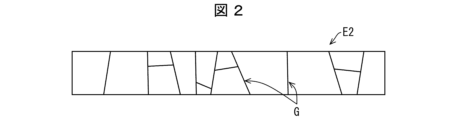
- 2 is a cross-sectional view showing a configuration example of a second electrode of the light-emitting element shown in FIG. 1 .
- FIG. 1 is a diagram citing Thornton's zone model showing the structural change of a sputtered thin film.
- FIG. 2 is a micrograph showing a cross section of one embodiment of the light-emitting element shown in FIG. 1 .
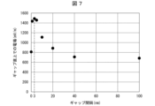
- FIG. 13 is a diagram showing the simulation results of the electric field distribution in a configuration with a gap spacing of 3 nm. 1 is a graph showing the particle diameter on the gap and the results of electric field amplification.
- FIG. 11 is a cross-sectional view showing a configuration example of a display device including a light-emitting element according to a second embodiment of the present disclosure.
- FIG. 11 is a cross-sectional view showing a configuration example of a display device including a light-emitting element according to a third embodiment of the present disclosure.
- FIG. 11 is a cross-sectional view showing a configuration example of a display device including a light-emitting element according to a fourth embodiment of the present disclosure.
- FIG. 13 is a cross-sectional view showing a configuration example of a display device including a light-emitting element according to a fifth embodiment of the present disclosure.
- FIG. 1 is a schematic diagram illustrating a configuration example of a display device according to an embodiment. 1 is a cross-sectional view showing a configuration example of a display device according to an embodiment.
- FIG. 1 is a cross-sectional view showing a configuration example of a display device 101 including a light-emitting element 10 according to an embodiment of the present disclosure.
- the display device 101 includes a light-emitting element 10 and a pixel circuit substrate 20 for driving the light-emitting element 10.
- the light-emitting element 10 is provided on the pixel circuit substrate 20.
- the light-emitting element 10 includes a first electrode E1, a second electrode E2 facing the first electrode E1, and a light-emitting layer Em located between the first electrode E1 and the second electrode E2.
- the light-emitting element 10 includes a first charge functional layer (ETL) F1 located between the first electrode E1 and the light-emitting layer Em, a second charge functional layer (HTL) F2 located between the second electrode E2 and the light-emitting layer Em, and a particle layer P1 located between the second electrode E2 and the pixel circuit substrate 20.
- the shape of the particles P contained in the particle layer P1 is not particularly limited, and is not limited to a spherical three-dimensional shape (circular cross-sectional shape). For example, it may be a polygonal cross-sectional shape, a rod-like three-dimensional shape, a branch-like three-dimensional shape, a three-dimensional shape with unevenness on the surface, or a combination thereof.
- the particle size for example, the diameter value of a circle having an area equivalent to the cross-sectional area of each particle is calculated from the cross-sectional observation of 50 adjacent particles, and the average of the diameter values of the 50 particles can be used as the particle size.
- the first electrode E1 is a light-reflecting electrode (light-reflecting cathode), and the second electrode E2 is a light-transmitting electrode (light-transmitting anode).
- the first electrode E1 is a light-reflecting electrode located above the second electrode E2, and the particle layer P1 is in contact with the lower surface of the second electrode E2.
- the upper layer is a layer located farther from the pixel circuit board 20 than the layer to be compared.
- the second electrode E2 is made of a metal-containing layer having a gap G penetrating the layer.
- the light-emitting layer Em includes a plurality of quantum dots.
- the first charge functional layer F1 and the second charge functional layer F2 may each include one or more functional layers such as a charge injection layer, a charge transport layer, and a charge shielding layer.
- the particle layer P1 is conductive, is in contact with the lower surface of the second electrode E2, and contains a plurality of metal oxide particles, such as titanium oxide particles P.
- the pixel circuit substrate 20 is an active substrate on which circuit elements and wiring are provided.
- the gap G of the metal-containing layer constituting the second electrode E2 will be described in detail later.
- the light-emitting element 10 shown in FIG. 1 will be described with respect to a configuration in which a particle layer P1, a second electrode E2, a second charge functional layer F2, a light-emitting layer Em, a first charge functional layer F1, and a first electrode E1 are stacked in this order on a pixel circuit substrate 20.
- the light-emitting element 10 is a bottom-emission type
- the first electrode E1 is a cathode
- the second electrode E2 is an anode.
- the light-emitting element 10 may be a top-emission type.
- the first charge functional layer F1 includes a hole transport layer HTL.
- the hole transport layer HTL is composed of a hole transport material that can stabilize the transport of holes into the light emitting layer Em.
- hole transport materials include poly[(9,9-dioctylfluorenyl-2,7-diyl)-co-(4,4'-(N-(4-sec-butylphenyl))diphenylamine)] (TFB) and poly[N,N'-bis(4-butylphenyl)-N,N'-bis(phenyl)benzidine] (poly-TPD). These hole transport materials may be used alone or in a suitable mixture of two or more types.
- the second charge functional layer F2 includes an electron transport layer ETL.
- the electron transport layer ETL is composed of an electron transporting material that can stabilize the transport of electrons into the light emitting layer Em.
- electron transporting materials include MgZnO, as well as nanoparticles containing one or more elements selected from the group consisting of Zn, Mg, Ti, Si, Sn, W, Ta, Ba, Zr, Al, Y, and Hf. These electron transporting materials may be used alone or in a suitable mixture of two or more types.
- the light-emitting layer Em is an organic light-emitting layer or a quantum dot light-emitting layer.
- the light-emitting element having an organic light-emitting layer as the light-emitting layer Em is an OLED (Organic Light Emitting Diode)
- the light-emitting element having a quantum dot light-emitting layer as the light-emitting layer Em is a QLED (Quantum dot Light Emitting Diode).
- the quantum dot means a dot having a maximum width of 100 nm or less.
- the shape of the quantum dot may be within a range that satisfies the maximum width, and is not particularly limited, and is not limited to a spherical three-dimensional shape (circular cross-sectional shape).
- it may be a polygonal cross-sectional shape, a rod-shaped three-dimensional shape, a branch-shaped three-dimensional shape, or a three-dimensional shape having unevenness on the surface, or a combination thereof.
- the gap G is a region that does not contain the material of the second electrode E2 (metal-containing layer) and penetrates the second electrode E2 (metal-containing layer) in the thickness direction. This region contains at least one of air, argon gas, and the material directly above the second electrode E2.
- the gap G allows cross-sectional observation of the structure using a SEM, a TEM, or the like, and also allows elements of the attached gas to be identified by elemental analysis using EDX or gas chromatography.
- FIG. 2 is a cross-sectional view showing an example of the configuration of the second electrode E2 of the light-emitting element 10 shown in Fig. 1.
- Fig. 3 is a diagram quoting Thornton's zone model showing a structural change of a sputtered thin film.
- Fig. 4 is a micrograph showing a cross section of one embodiment of the light-emitting element 10 shown in Fig. 1.
- the gap G penetrates the metal-containing layer constituting the second electrode E2.
- the gap G may have any shape as long as it penetrates the second electrode E2.
- the gap G may be linear or curved.
- the gap G may be parallel or oblique to the layer thickness direction.
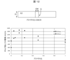
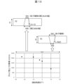
- FIGS. 12 and 13 are data showing the relationship between the gap shape and the strength of the electric field directly above the gap.
- the gap G formed in the second electrode E2 preferably has a ratio (aspect ratio) of the gap width GW to the thickness D of the second electrode E2 of 1.0 or less.
- the gap width GW may be an average width in the entire gap length. As shown in FIG.
- the gap G is located on one surface of the second electrode E2, and the width WA of the opening KA facing the particle layer P1 is preferably smaller than the width WB of the opening KB located on the other surface of the second electrode E2 and not facing the particle layer P1.
- tan ⁇ (WA ⁇ WB)/2D, where D is the thickness of the second electrode E2 (metal-containing layer), and it can be seen that when the inclination angle ⁇ 0, the electric field immediately above the gap is enhanced.
- the gap G penetrating the second electrode E2 can be introduced by adjusting the sputtering conditions (temperature, pressure) when the second electrode E2 is formed by sputtering instead of general vapor deposition.
- the temperature of the glass substrate is set to a high temperature of about 200° C., and argon gas is introduced to form a film of the material of the second electrode E2 at a pressure of about 1 Pa.
- Al (aluminum) or Ag (silver) is suitable as the material of the second electrode E2. Therefore, the second electrode E2 contains aluminum or silver.
- the sputtering conditions and the state of the film are known as the Thornton zone model in FIG. 3, and the interval of the gap G can be controlled according to this zone model.
- the gap G can be introduced into the second electrode E2. If the gap G is to be introduced into the second electrode E2, the sputtering conditions of ZONE II of the Thornton zone model shown in FIG. 3 are preferable.
- the shape of the gap G created under the condition of ZONE II is formed to be a shape along the layer thickness direction, but is not limited to ZONE II, and ZONE III is also applicable.
- the light-emitting element 10 has a laminated structure of the second charge functional layer (HTL) F2, the light-emitting layer Em, and the first charge functional layer (ETL) F1, which are formed by general coating or inkjet printing, and finally the first electrode E1 (cathode) is vacuum-deposited to seal the element structure.
- HTL second charge functional layer
- Em the light-emitting layer
- ETL first charge functional layer
- Figure 4 shows a cross-sectional SEM image of the light-emitting element 10 manufactured in this manner. As shown in Figure 4, the gap G in the second electrode E2 can be seen.
- the gap G exists in the second electrode E2.
- gap plasmons are excited in the gap G.
- Gap plasmons are light localized in the gap G, and are converted into propagating light when particles P of the particle layer P1 are present in the range in which this light is distributed (the range that seeps out from the gap G). In other words, it is preferable that the particles P are present on the gap G.
- the multiple particles P contained in the particle layer P1 scatter light amplified by plasmons generated in the gap G.
- Figure 5 shows the results of simulating the electric field distribution near the gap G formed in the second electrode E2, which is an Ag layer with a thickness of 20 nm.
- the second electrode E2 is an Ag layer with a thickness of 20 nm.
- the gap G spacing in this case was 3 nm.
- the gap G spacing is the average width at the opening surface of the opening formed by the gap G on the surface of the second electrode E2. For example, if the gap G is cylindrical, the gap G spacing is equal to the diameter of the cylinder.
- the gap G spacing can be explained as the diameter of the gap G. Also, if the through hole is elliptical, the gap G spacing can be explained as the average diameter of the major axis and the minor axis.
- a second charge functional layer (HTL) with a thickness of 10 nm and a refractive index of 1.4, and below that is an emission surface for a plane wave with a wavelength of 400 nm excited by an electric field of 1 V/m.
- the particle layer P1 is omitted, and a layer with a refractive index of 1.5 is set up to the edge of the simulation area as the pixel circuit board 20.
- gap plasmon a strong electric field (gap plasmon) is excited in the gap G, which has a very narrow gap of 3 nm, for light with a wavelength of 400 nm from the emission surface side, and light leaks out to the upper surface of the gap G (the pixel circuit board 20 side).
- FIG. 6 shows the results of simulating the electric field amplification at the end of the simulation region in a configuration in which the TiO 2 particles P in the particle layer P1 are on the gap G.
- a diameter of the TiO 2 particles of 0 nm means a configuration in which there are no TiO 2 particles. From this simulation result, it can be seen that in a configuration in which TiO 2 particles are present, if the diameter of the TiO 2 particles is 60 nm or less, the intensity is amplified by scattering the leaked light of the gap plasmon. On the other hand, if the diameter of the TiO 2 particles is larger than 60 nm, it can be seen that the gap plasmon is difficult to excite, and therefore the effect is lost. Therefore, it is preferable that the average particle diameter of the particles P in the particle layer P1 is 60 nm or less. Furthermore, it is preferable that the average particle diameter of the particles P is 1/10 of the emission peak wavelength at which forward scattering becomes strong.
- gap plasmons are excited in the gap G introduced in the second electrode E2, and are scattered by the multiple particles P in the particle layer P1, thereby improving the transmittance (light extraction efficiency) of the light from the light-emitting layer Em through the second electrode E2.
- the graph shown in FIG. 7 plots the relationship between the gap interval and the electric field strength excited directly above the gap G, by changing the gap interval (hereinafter referred to as the gap interval). From this graph, it can be seen that a strong electric field is generated with a peak at a gap interval of 3 nm.
- a gap interval of 0 nm is a configuration without a gap G, and the range in which the electric field is 800 mV/m or more at this time is the range in which the gap G is effective. Therefore, it can be seen that a gap interval of 20 nm or less is preferable to increase the light extraction efficiency.
- the average particle size of the particles P of the particle layer P1 is preferably 60 nm or less.
- a second electrode E2 is formed that combines high electrical conductivity (small work function) due to the metal, high light extraction efficiency, and high reliability (no leakage or discontinuity due to unevenness), and a particle layer P1 is formed by normal coating or the like, thereby making it possible to obtain a light-emitting element 10 that simultaneously satisfies the following:
- the gap plasmons excited in the gap G can be converted into propagating light, improving the light extraction efficiency from the second electrode E2.
- the surface of the second electrode E2, including the gap G, has small irregularities, so the layer deposited on it does not break, and leaks, discontinuities, etc. do not occur.
- the second electrode E2 is an anode, and an example is described in which the second electrode E2 and the particle layer P1 are characterized.
- the same effect can be achieved even if the second electrode E2 is a cathode, as long as a gap G is provided in the same way and particles P are contained in the particle layer P1.
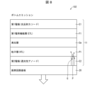
- FIG. 8 is a cross-sectional view showing a configuration example of a display device 102 including a light-emitting element 11 according to another embodiment of the present disclosure.
- the display device 102 has the same pixel circuit substrate 20 as the display device 101 of the first embodiment, but has a different laminated structure of the light-emitting element 11.
- the light-emitting element 11 has a second electrode E2, a particle layer P1, a light-emitting layer Em, a first charge functional layer F1, and a first electrode E1 laminated in this order on the pixel circuit substrate 20.
- the members marked with the same reference numerals as those of the light-emitting element 10 of the first embodiment have the same functions, and therefore detailed description thereof will be omitted.
- the light-emitting element 11 has the same positional relationship between the first electrode E1 and the second electrode E2 as the light-emitting element 10 shown in FIG. 1, but is different in that the second electrode E2 is formed directly above the pixel circuit substrate 20 instead of the particle layer P1, and the particle layer P1 is formed on the second electrode E2.
- the particle layer P1 is formed so as to be in contact with the upper surface of the second electrode E2.
- the particle layer P1 functions as a hole transport layer HTL. That is, the particle layer P1 contains, as particles P, metal oxide particles having a hole transport function.
- the metal oxide is preferably, for example, nickel oxide, and in this case, the particles P contained in the particle layer P1 are nickel oxide particles.
- the average width (gap spacing) at the opening surface of the opening formed in the surface of the second electrode E2 by penetration through the gap G is set to be equal to or smaller than the average particle size of the multiple particles P contained in the particle layer P1 above the second electrode E2. Therefore, based on the graph of FIG. 7 described in embodiment 1, the gap spacing is preferably equal to or smaller than 20 nm, and is preferably equal to or smaller than the average particle size of the particles P contained in the particle layer P1.
- the display device 102 having the above configuration is provided with a gap G in the second electrode E2 and a particle layer P1 containing particles P, similar to the display device 101 of the first embodiment. Therefore, the display device 102 has the same effect as the display device 101 of the first embodiment. That is, by adjusting the sputtering conditions, the second electrode E2 having high electrical conductivity (small work function) due to metal, high light extraction efficiency, and high reliability (no leakage or discontinuity due to unevenness) is formed, and the particle layer P1 is formed by normal coating or the like, thereby making it possible to obtain a light-emitting element 11 that simultaneously satisfies the following.
- the gap plasmons excited in the gap G can be converted into propagating light, improving the light extraction efficiency from the second electrode E2.
- the surface of the second electrode E2, including the gap G, has small irregularities, so the layer deposited on it does not break, and leaks, discontinuities, etc. do not occur.
- the second electrode E2 is an anode, and an example is described in which the second electrode E2 and the particle layer P1 are characterized.
- the same effect can be achieved even if the second electrode E2 is a cathode, as long as a gap G is provided in the same way and particles P are contained in the particle layer P1.
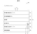
- FIG. 9 is a cross-sectional view showing a configuration example of a display device 103 including a light-emitting element 12 according to another embodiment of the present disclosure.
- the display device 103 has the same pixel circuit substrate 20 and the same stacked structure of the light-emitting element 11 as the display device 102 of the second embodiment, but the functions of the first electrode E1 and the second electrode E2 are different.
- the first electrode E1 is located in a layer above the second electrode E2 and is a translucent electrode (translucent cathode).
- the second electrode E2 has a plurality of gaps G and is a light-reflecting electrode (light-reflecting anode). Therefore, the display device 103 is a so-called top-emission type display device in which light is emitted from the first electrode E1 stacked at the position farthest from the pixel circuit substrate 20.
- the light-emitting element 12 has the same positional relationship between the first electrode E1 and the second electrode E2 as the light-emitting element 10 shown in FIG. 1, but is different in that the second electrode E2 is formed directly above the pixel circuit substrate 20 instead of the particle layer P1, and the particle layer P1 is formed on the second electrode E2.
- the particle layer P1 is formed so as to be in contact with the upper surface of the second electrode E2.
- the particle layer P1 functions as a hole transport layer HTL. That is, the particle layer P1 contains, as particles P, metal oxide particles having a hole transport function.
- the metal oxide is preferably, for example, nickel oxide, and in this case, the particles P contained in the particle layer P1 are nickel oxide particles.
- the display device 103 having the above configuration is provided with a gap G in the second electrode E2 and a particle layer P1 containing particles P, similar to the display device 102 of the second embodiment. Therefore, the display device 103 has the same effect as the display device 102 of the second embodiment, except that the display device 103 is a bottom emission type or a top emission type. That is, by adjusting the sputtering conditions, the second electrode E2 having high electrical conductivity (small work function) due to metal, high light extraction efficiency, and high reliability (no leakage or discontinuity due to unevenness) is formed, and the particle layer P1 is formed by normal coating, etc., to obtain a light-emitting element 11 that simultaneously satisfies the following.
- the gap plasmons excited in the gap G can be converted into propagating light, improving the light extraction efficiency from the second electrode E2.
- the surface of the second electrode E2, including the gap G, has small irregularities, so the layer deposited on it does not break, and leaks, discontinuities, etc. do not occur.
- the second electrode E2 is an anode, and an example is described in which the second electrode E2 and the particle layer P1 are characterized.
- the same effect can be achieved even if the second electrode E2 is a cathode, as long as a gap G is provided in the same way and particles P are contained in the particle layer P1.
- Fig. 10 is a cross-sectional view showing a configuration example of a display device 104 including a light-emitting element 13 according to another embodiment of the present disclosure.
- the display device 104 has the same pixel circuit substrate 20 as the display device 103 of the third embodiment, but has a different layer structure of the light-emitting element 13.
- the light-emitting element 13 has a first electrode E1, a second charge functional layer F2, a light-emitting layer Em, a particle layer P1, and a second electrode E2 layered in this order on the pixel circuit substrate 20.
- the light-emitting element 13 differs from the light-emitting element 12 shown in FIG. 9 in that the positions of the first electrode E1, the second electrode E2, and the particle layer P1 are interchanged. Therefore, when the pixel circuit board 20 is the bottom layer, the first electrode E1 is located lower than the second electrode E2 and is a light-reflecting electrode (light-reflecting anode). The particle layer P1 is formed so as to be in contact with the lower surface of the second electrode E2. On the other hand, the second electrode E2 has a plurality of gaps G and is a translucent electrode (translucent cathode).
- the display device 104 is a so-called top-emission display device in which light is emitted from the second electrode E2 stacked at the position farthest from the pixel circuit board 20.
- the particle layer P1 functions as an electron transport layer ETL. That is, the particle layer P1 contains, as particles P, particles of a metal oxide having an electron transport function.
- the metal oxide is, for example, zinc oxide. If it has electronic functionality, the metal oxide is not limited to zinc oxide and may be titanium oxide.
- the display device 104 having the above configuration is provided with a gap G in the second electrode E2 and a particle layer P1 containing particles P, similar to the display device 103 of the third embodiment. Therefore, the display device 102 has the same effect as the display device 103 of the third embodiment. That is, by adjusting the sputtering conditions, the second electrode E2 having high electrical conductivity (small work function) due to metal, high light extraction efficiency, and high reliability (no leakage or discontinuity due to unevenness) is formed, and the particle layer P1 is formed by normal coating or the like, thereby making it possible to obtain a light-emitting element 11 that simultaneously satisfies the following.
- the electrode can have a small work function suitable for injecting electrons into the particle layer P1 (ETL). In other words, the efficiency of electron injection into the light-emitting layer Em can be improved.
- the gap plasmon excited in the gap G can be converted into propagating light, thereby improving the efficiency of extracting light from the second electrode E2.
- the surface of the second electrode E2, including the gap G, has small irregularities, so the layer deposited on it does not break, and leaks, discontinuities, etc. do not occur.
- FIG. 11 is a cross-sectional view showing a configuration example of a display device 105 including a light-emitting element 14 according to another embodiment of the present disclosure.
- the display device 105 is different from the display device 101 of the first embodiment in that it includes another particle layer P2 instead of the second charge functional layer F2.
- This another particle layer P2 functions as a hole transport layer (HTL) and also contains a plurality of metal oxide particles.
- the metal oxide particles for example, nickel oxide particles are included.
- the another particle layer P2 is formed on the upper surface of the second electrode E2.
- the light emitting element 14 includes a particle layer P1 in contact with one of the upper and lower surfaces of the second electrode E2, and another particle layer P2 in contact with the other.
- layers containing particles P are stacked on the upper and lower surfaces of the second electrode E2, so that gap plasmons excited in the gap G of the second electrode E2 can be converted into propagating light by the particles P on both the upper and lower surfaces of the second electrode E2. This can significantly improve the light extraction efficiency from the second electrode E2.
- the display device 105 having the above-described configuration has the same effects as those of the other embodiments, except for the above-described effects. That is, by adjusting the sputtering conditions, the second electrode E2 having high electrical conductivity (small work function) due to metal, high light extraction efficiency, and high reliability (no leakage or discontinuity due to unevenness) is formed, and the particle layer P1 is formed by normal coating or the like, thereby making it possible to obtain the light-emitting element 11 that simultaneously satisfies the following:
- the surface of the second electrode E2, including the gap G, has small irregularities, so the layer deposited on it does not break, and leaks, discontinuities, etc. do not occur.
- the above-mentioned configuration makes it possible to simultaneously increase the efficiency of electron injection into the light-emitting layer and the efficiency of light extraction, and to form a film on the electrode layer without causing film breakage. This effect also contributes to the achievement of Goal 12 of the Sustainable Development Goals (SDGs) advocated by the United Nations, "Ensure sustainable consumption and production patterns.”
- SDGs Sustainable Development Goals
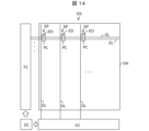
- FIG. 14 is a schematic diagram showing a configuration example of a display device according to an embodiment.
- FIG. 15 is a cross-sectional view showing a configuration example of a display device according to an embodiment.
- the display device 105 includes a display unit DA including a plurality of subpixels SP, a first driver X1 and a second driver X2 that drive the plurality of subpixels SP, and a display control unit DC that controls the first driver X1 and the second driver X2.
- the subpixel SP includes a light-emitting element 10 and a pixel circuit PC that is connected to the light-emitting element 10.
- the pixel circuit PC may be connected to a scanning signal line GL, a data signal line DL, and a light-emitting control line EL.
- the scanning signal line GL and the light-emitting control line EL may be connected to the first driver X1, and the data signal line DL may be connected to the second driver X2.
- the light-emitting element 10 is an example, and the light-emitting element 10 may be replaced with any of the light-emitting elements 11, 12, 13, and 14 to form the display devices 101, 102, 103, and 104.
- the display device 101 may include a pixel circuit substrate 13 including a substrate 11 and a pixel circuit layer 12, a light emitting element layer 14, and a sealing layer 15.
- the substrate 11 may be a glass substrate, a resin substrate, or the like.
- the substrate 11 may be flexible.
- the pixel circuit layer 12 includes a plurality of pixel circuits PC arranged, for example, in an inorganic matrix.
- the pixel circuit PC may include a pixel capacitance to which a grayscale signal is written, a transistor that controls a current value of the light emitting element ED in response to the grayscale signal, a transistor connected to a scanning signal line GL and a data signal line DL, and a transistor connected to a light emission control line EL.
- the display device DS includes a pixel circuit board 13 and a light emitting element layer 14.
- the light emitting element layer 14 may include, in order from the pixel circuit board 13 side, a first electrode E1, an edge cover film JF covering the edge of the first electrode E1, a first functional layer FK, a light emitting layer (quantum dot layer) Em, a second functional layer SK, and a second electrode E2.
- the first functional layer FK may have a hole injection function and a hole transport function
- the second functional layer SK may have an electron transport function.
- the light emitting element layer 14 may include a light emitting element ED including a light emitting layer Em that emits red light, a light emitting element ED including a light emitting layer Em that emits green light, and a light emitting element ED including a light emitting layer Em that emits blue light.
- the sealing layer 15 includes an inorganic insulating film such as a silicon nitride film or a silicon oxide film, and prevents foreign matter (water, oxygen, etc.) from entering the light emitting element layer 14.
- the light-emitting element ED may be any of the light-emitting elements 10 to 14 described above, and the display device DS may be any of the display devices 101 to 105.
Landscapes
- Physics & Mathematics (AREA)
- Optics & Photonics (AREA)
- Chemical & Material Sciences (AREA)
- Engineering & Computer Science (AREA)
- Crystallography & Structural Chemistry (AREA)
- Inorganic Chemistry (AREA)
- Nanotechnology (AREA)
- Electroluminescent Light Sources (AREA)
Abstract
Description
(発光素子の概要)
図1は、本開示の一実施形態に係る発光素子10を備えた表示装置101の構成例を示す断面図である。図1に示すように、表示装置101は、発光素子10と、発光素子10を駆動するための画素回路基板20とを含む。発光素子10は、画素回路基板20上に設けられている。発光素子10は、第1電極E1と、第1電極E1と対向する第2電極E2と、第1電極E1および第2電極E2の間に位置する発光層Emとを備える。発光素子10は、第1電極E1および発光層Emとの間に位置する第1電荷機能層(ETL)F1、第2電極E2および発光層Emとの間に位置する第2電荷機能層(HTL)F2、および、第2電極E2および画素回路基板20との間に位置する粒子層P1を備える。
粒子層P1に含まれる粒子Pの形状は、特に制約されず、球状の立体形状(円状の断面形状)に限定されるものではない。例えば、多角形状の断面形状、棒状の立体形状、枝状の立体形状、表面に凹凸を有する立体形状でもよく、または、それらの組合せでもよい。粒子径については、例えば近接する50個の粒子の断面観察から、各粒子の断面面積に相当する面積を有する円の直径値を算出し、50個の直径値の平均を粒子径とすることができる。
ギャップGは、第2電極E2(金属含有層)の材料を含まず、第2電極E2(金属含有層)を厚み方向に貫通する領域である。この領域には、空気、アルゴンガス、第2電極E2直上の材料の少なくとも1つが含まれる。例えばギャップGは、SEM、TEMなどにより構造の断面観察が可能であり、また、EDXやガスクロマトグラフィーによる元素分析で、付着ガスの元素を特定可能である。
図2は、図1に示す発光素子10の第2電極E2の構成例を示す断面図である。図3は、スパッタ薄膜の構造変化を示すThorntonのゾーンモデルを引用する図である。図4は、図1に示した発光素子10の一実施例の断面を撮像した顕微鏡写真を示す図である。
このように第2電極E2を貫通するギャップGは、第2電極E2を一般的な蒸着ではなくスパッタ成膜を行う際のスパッタ条件(温度、圧力)を調整することで導入することができる。例えば、第2電極E2をスパッタ成膜する際、ガラス基板の温度を200℃程度の高温とし、アルゴンガスを導入して1Pa程度の圧力として第2電極E2の材料を成膜する。このときの第2電極E2の材料はAl(アルミニウム)やAg(銀)が適する。従って、第2電極E2は、アルミニウムまたは銀を含む。スパッタ条件と膜の状態は図3のThorntonのゾーンモデルとして知られており、このゾーンモデルに従い、ギャップGの間隔を制御することができる。アルゴン分圧を固定して基板温度を下げれば層の厚さ方向に連続し柱状に近い膜が生成され、すなわち第2電極E2にギャップGを導入することができる。第2電極E2にギャップGを導入するのであれば、図3に示すThorntonのゾーンモデルのZONEIIのスパッタ条件が好ましい。ZONEIIの条件で作成されたギャップGの形状は、層厚方向に沿う形状に形成される。もっともZONEIIに限定されず、ZONEIIIも適用可能である。
上述の通り、第2電極E2にギャップGが存在する。発光層Emからの光が第2電極E2に入射することで、ギャップGにおいてギャッププラズモンが励起される。ギャッププラズモンとは、ギャップGに局在した光であるが、この光が分布している範囲(ギャップGから浸みだした範囲)に粒子層P1の粒子Pがあることで、伝搬光に変換される。すなわち、ギャップG上に粒子Pがあることが好ましい。
「ギャップ上」については、粒子Pの少なくとも一部がギャップGの間隔の範囲に存在すること、第2電極E2の表面に形成されるギャップGにおいて、ギャップGの間隔に対する粒子層P1の範囲に粒子Pの少なくとも一部が存在することが確認できればよい。つまり、粒子層P1に含まれる複数の粒子Pは、ギャップGで生じたプラズモンにより増幅された光を散乱する。
図7に示すグラフは、ギャップGの間隔(以下、ギャップ間隔と称する)を変えてシミュレーションし、ギャップG直上に励起された電場強度とギャップ間隔との関係をプロットしたものである。このグラフから、ギャップ間隔が3nmをピークとして強い電場が発生していることがわかる。ここで、ギャップ間隔0nmは、ギャップGがない構成であり、このときの電場800mV/m以上となる範囲がギャップGによる効果がある範囲である。よって、光取出し効率を高めるためには、20nm以下のギャップ間隔が好ましいとわかる。この場合、粒子層P1の粒子Pの平均粒子径は60nm以下が好ましい。
以上のことから、スパッタ条件の調整により、金属による高い電気伝導性(小さな仕事関数)と、高い光取出し効率と、高信頼性(凹凸によるリークや断絶などが起きない)を兼ね備えた第2電極E2を形成し、通常の塗布などにより粒子層P1を形成することで、以下を同時に満たす発光素子10にできる。
図8は、本開示の他の実施形態に係る発光素子11を備えた表示装置102の構成例を示す断面図である。図8に示すように、表示装置102は、前記実施形態1の表示装置101と比較して、画素回路基板20は同じであり、発光素子11の積層構造が異なっている。具体的には、発光素子11は、画素回路基板20上に、第2電極E2、粒子層P1、発光層Em、第1電荷機能層F1、第1電極E1が順に積層されている。なお、前記実施形態1の発光素子10と同じ符号付記した部材は同じ機能を有しているので、詳細な説明は省略する。
前記構成の表示装置102は、前記実施形態1の表示装置101と同様に、第2電極E2にギャップGを設けて、粒子Pを含む粒子層P1を設けている。従って、表示装置102は、前記実施形態1の表示装置101と同様の効果を奏する。すなわち、スパッタ条件の調整により、金属による高い電気伝導性(小さな仕事関数)と、高い光取出し効率と、高信頼性(凹凸によるリークや断絶などが起きない)を兼ね備えた第2電極E2を形成し、通常の塗布などにより粒子層P1を形成することで、以下を同時に満たす発光素子11にできる。
図9は、本開示の他の実施形態に係る発光素子12を備えた表示装置103の構成例を示す断面図である。図9に示すように、表示装置103は、前記実施形態2の表示装置102と比較して、画素回路基板20は同じであり、発光素子11の積層構造が同じであるが、第1電極E1および第2電極E2の機能が異なっている。具体的には、第1電極E1は、第2電極E2よりも上層に位置し、かつ、透光性電極(透光性カソード)である。一方、第2電極E2は、ギャップGを複数有し、かつ、光反射電極(光反射アノード)である。従って、表示装置103は、画素回路基板20から一番遠い位置に積層された第1電極E1から光が放射される、所謂トップエミッション型の表示装置である。
前記構成の表示装置103は、前記実施形態2の表示装置102と同様に、第2電極E2にギャップGを設けて、粒子Pを含む粒子層P1を設けている。従って、表示装置103は、前記実施形態2の表示装置102とボトムエミッション型かトップエミッション型かの違いだけであり、前記実施形態2の表示装置102と同様の効果を奏する。すなわち、スパッタ条件の調整により、金属による高い電気伝導性(小さな仕事関数)と、高い光取出し効率と、高信頼性(凹凸によるリークや断絶などが起きない)を兼ね備えた第2電極E2を形成し、通常の塗布などにより粒子層P1を形成することで、以下を同時に満たす発光素子11にできる。
図10は、本開示の他の実施形態に係る発光素子13を備えた表示装置104の構成例を示す断面図である。図10に示すように、表示装置104は、前記実施形態3の表示装置103と比較して、画素回路基板20は同じであり、発光素子13の積層構造が異なっている。具体的には、発光素子13は、画素回路基板20上に、第1電極E1、第2電荷機能層F2、発光層Em、粒子層P1、第2電極E2が順に積層されている。
前記構成の表示装置104は、前記実施形態3の表示装置103と同様に、第2電極E2にギャップGを設けて、粒子Pを含む粒子層P1を設けている。従って、表示装置102は、前記実施形態3の表示装置103と同様の効果を奏する。すなわち、スパッタ条件の調整により、金属による高い電気伝導性(小さな仕事関数)と、高い光取出し効率と、高信頼性(凹凸によるリークや断絶などが起きない)を兼ね備えた第2電極E2を形成し、通常の塗布などにより粒子層P1を形成することで、以下を同時に満たす発光素子11にできる。
光取出し効率を向上できる。
図11は、本開示の他の実施形態に係る発光素子14を備えた表示装置105の構成例を示す断面図である。図11に示すように、表示装置105は、前記実施形態1の表示装置101と比較して、第2電荷機能層F2の代わりに別の粒子層P2を備えている点で異なる。この別の粒子層P2は、正孔輸送層(HTL)として機能する他に、金属酸化物の粒子を複数含んでいる。金属酸化物の粒子として、例えば酸化ニッケルの粒子を含んでいる。また、別の粒子層P2は、第2電極E2の上面に形成されている。
前記構成の表示装置105は、上述した効果の他の効果は、他の実施形態と同様の効果を奏する。すなわち、スパッタ条件の調整により、金属による高い電気伝導性(小さな仕事関数)と、高い光取出し効率と、高信頼性(凹凸によるリークや断絶などが起きない)を兼ね備えた第2電極E2を形成し、通常の塗布などにより粒子層P1を形成することで、以下を同時に満たす発光素子11にできる。
表示装置101は、基板11および画素回路層12を含む画素回路基板13と、発光素子層14と、封止層15とを含んでよい。基板11にはガラス基板、樹脂基板等を用いることができる。基板11が可撓性であってもよい。画素回路層12は、例えば無機マトリクス配置された複数の画素回路PCを含む。画素回路PCは、階調信号が書き込まれる画素容量と、階調信号に応じて発光素子EDの電流値を制御するトランジスタと、走査信号線GLおよびデータ信号線DLに接続するトランジスタと、発光制御線ELに接続するトランジスタとを含んでよい。
図15に示すように、表示装置DSは、画素回路基板13および発光素子層14を含む。発光素子層14は、画素回路基板13側から順に、第1電極E1、第1電極E1のエッジを覆うエッジカバー膜JF、第1機能層FK、発光層(量子ドット層)Em、第2機能層SK、および第2電極E2を含んでよい。第1機能層FKは、正孔注入機能および正孔輸送機能を有し、第2機能層SKは、電子輸送機能を有してよい。発光素子層14は、赤色光を発する発光層Emを含む発光素子EDと、緑色光を発する発光層Emを含む発光素子EDと、青色光を発する発光層Emを含む発光素子EDとを備えてもよい。封止層15は、窒化シリコン膜、酸化シリコン膜等の無機絶縁膜を含み、異物(水、酸素等)が発光素子層14に侵入することを防ぐ。発光素子EDは、上述の発光素子10~14のいずれかであってよく、表示装置DSは、表示装置101~105のいずれかであってよい。
20 画素回路基板
101、102、103、104、105 表示装置
E1 第1電極
E2 第2電極
Em 発光層
F1 第1電荷機能層
F2 第2電荷機能層
P1 粒子層
P2 別の粒子層
Claims (29)
- 第1電極と、
層内を貫通するギャップを有する金属含有層からなる第2電極と、
前記第1電極および前記第2電極の間に位置する発光層と、
粒子を含み、前記第2電極に接する粒子層と、を備える、発光素子。 - 前記ギャップの貫通によって前記金属含有層の表面に形成された開口の開口面における平均幅は、20〔nm〕以下である、請求項1に記載の発光素子。
- 前記ギャップの貫通によって前記金属含有層の表面に形成された開口の開口面における平均幅は、前記粒子の粒径以下である、請求項1に記載の発光素子。
- 前記第1電極は、前記第2電極よりも上層に位置する光反射電極であり、
前記粒子層は、前記第2電極の下面に接する、請求項1~3のいずれか1項に記載の発光素子。 - 前記粒子は、金属酸化物であり、導電性を有する、請求項4に記載の発光素子。
- 前記金属酸化物は、酸化チタンである、請求項5に記載の発光素子。
- 前記第1電極は、前記第2電極よりも上層に位置する光反射電極であり、
前記粒子層は、前記第2電極の上面に接する、請求項1~3のいずれか1項に記載の発光素子。 - 前記粒子は、金属酸化物であり、正孔輸送機能を有する、請求項7に記載の発光素子。
- 前記金属酸化物は、酸化ニッケルである、請求項8に記載の発光素子。
- 前記第1電極は、前記第2電極よりも上層に位置する透光性電極であり、
前記粒子層は、前記第2電極の上面に接する、請求項1~3のいずれか1項に記載の発光素子。 - 前記粒子は、金属酸化物であり、正孔輸送機能を有する、請求項10に記載の発光素子。
- 前記金属酸化物は、酸化ニッケルである、請求項11に記載の発光素子。
- 前記第2電極はアノードである、請求項4~12のいずれか1項に記載の発光素子。
- 前記第2電極は、アルミニウムまたは銀を含む、請求項4~13のいずれか1項に記載の発光素子。
- 前記第1電極は、前記第2電極よりも下層に位置する光反射電極であり、
前記粒子層は、前記第2電極の下面に接する、請求項1~3のいずれか1項に記載の発光素子。 - 前記粒子は、金属酸化物であり、電子輸送機能を有する、請求項15に記載の発光素子。
- 前記金属酸化物は、酸化亜鉛である、請求項16に記載の発光素子。
- 前記金属酸化物は、酸化チタンである、請求項16に記載の発光素子。
- 前記第2電極はカソードである、請求項15~18のいずれか1項に記載の発光素子。
- 前記粒子の粒径は、60〔nm〕以下である、請求項1~19のいずれか1項に記載の発光素子。
- 前記粒子の粒径は、前記発光層の発光ピーク波長の1/10以下である、請求項1~19のいずれか1項に記載の発光素子。
- 前記ギャップは、前記第2電極の厚さに対するギャップ幅の比が1.0以下である、請求項1~21のいずれか1項に記載の発光素子。
- 前記ギャップ上に前記粒子の少なくとも一部が位置する、請求項1~22のいずれか1項に記載の発光素子。
- 前記ギャップは、前記第2電極の層厚方向に沿う形状である、請求項1~23のいずれか1項に記載の発光素子。
- 前記ギャップは、前記粒子層に面する開口の幅が、前記第2電極の他方の面に位置し、前記粒子層に面しない開口の幅よりも小さい、請求項1~24のいずれか1項に記載の発光素子。
- 前記第2電極の上面および下面の一方に接する前記粒子層と、他方に接する別の粒子層とを備える、請求項1~3のいずれか1項に記載の発光素子。
- 前記複数の粒子は、前記ギャップで生じたプラズモンにより増幅された光を散乱する、請求項1~26のいずれか1項に記載の発光素子。
- 前記発光層は、有機発光層または量子ドット発光層である、請求項1~27のいずれか1項に記載の発光素子。
- 請求項1~28のいずれか1項に記載の発光素子を備える、表示装置。
Priority Applications (2)
| Application Number | Priority Date | Filing Date | Title |
|---|---|---|---|
| PCT/JP2023/005935 WO2024176284A1 (ja) | 2023-02-20 | 2023-02-20 | 発光素子、表示装置 |
| CN202380090334.XA CN120435934A (zh) | 2023-02-20 | 2023-02-20 | 发光元件、显示装置 |
Applications Claiming Priority (1)
| Application Number | Priority Date | Filing Date | Title |
|---|---|---|---|
| PCT/JP2023/005935 WO2024176284A1 (ja) | 2023-02-20 | 2023-02-20 | 発光素子、表示装置 |
Publications (1)
| Publication Number | Publication Date |
|---|---|
| WO2024176284A1 true WO2024176284A1 (ja) | 2024-08-29 |
Family
ID=92500591
Family Applications (1)
| Application Number | Title | Priority Date | Filing Date |
|---|---|---|---|
| PCT/JP2023/005935 Ceased WO2024176284A1 (ja) | 2023-02-20 | 2023-02-20 | 発光素子、表示装置 |
Country Status (2)
| Country | Link |
|---|---|
| CN (1) | CN120435934A (ja) |
| WO (1) | WO2024176284A1 (ja) |
Citations (4)
| Publication number | Priority date | Publication date | Assignee | Title |
|---|---|---|---|---|
| JP2014167930A (ja) * | 2014-05-08 | 2014-09-11 | Toshiba Corp | 有機エレクトロルミネッセンス素子を用いた照明装置 |
| JP2015508218A (ja) * | 2012-02-10 | 2015-03-16 | サン−ゴバン グラス フランス | Oledのための透明支持電極 |
| US20170005235A1 (en) * | 2013-11-27 | 2017-01-05 | Princeton University | Light emitting diode, photodiode, displays, and method for forming the same |
| WO2017077933A1 (ja) * | 2015-11-06 | 2017-05-11 | リンテック株式会社 | 透明導電層積層用フィルム、その製造方法、及び透明導電性フィルム |
-
2023
- 2023-02-20 CN CN202380090334.XA patent/CN120435934A/zh active Pending
- 2023-02-20 WO PCT/JP2023/005935 patent/WO2024176284A1/ja not_active Ceased
Patent Citations (4)
| Publication number | Priority date | Publication date | Assignee | Title |
|---|---|---|---|---|
| JP2015508218A (ja) * | 2012-02-10 | 2015-03-16 | サン−ゴバン グラス フランス | Oledのための透明支持電極 |
| US20170005235A1 (en) * | 2013-11-27 | 2017-01-05 | Princeton University | Light emitting diode, photodiode, displays, and method for forming the same |
| JP2014167930A (ja) * | 2014-05-08 | 2014-09-11 | Toshiba Corp | 有機エレクトロルミネッセンス素子を用いた照明装置 |
| WO2017077933A1 (ja) * | 2015-11-06 | 2017-05-11 | リンテック株式会社 | 透明導電層積層用フィルム、その製造方法、及び透明導電性フィルム |
Also Published As
| Publication number | Publication date |
|---|---|
| CN120435934A (zh) | 2025-08-05 |
Similar Documents
| Publication | Publication Date | Title |
|---|---|---|
| CN101165941B (zh) | 发光面板和具有它的光源设备 | |
| US8389981B2 (en) | Organic light emitting diode lighting equipment | |
| KR101976065B1 (ko) | 유기발광표시장치 및 이의 제조방법 | |
| CN108461651A (zh) | 像素结构及其制备方法、显示面板 | |
| US11417851B2 (en) | Light-emitting element, light-emitting device, and device for producing light-emitting element | |
| US12484416B2 (en) | Light-emitting substrate and light-emitting apparatus | |
| WO2021164106A1 (zh) | 一种柔性显示面板及其制备方法 | |
| WO2022237096A1 (zh) | 一种发光基板及发光装置 | |
| CN120091731A (zh) | 显示面板和电子装置 | |
| JP2005157353A (ja) | 低抵抗配線を備える有機電界発光素子 | |
| US20220199716A1 (en) | Display device | |
| WO2024176284A1 (ja) | 発光素子、表示装置 | |
| CN221532026U (zh) | 显示面板及车尾灯 | |
| JP7741992B2 (ja) | 発光素子、表示装置、および発光素子の製造方法 | |
| CN119677345A (zh) | 显示面板及显示装置 | |
| CN214588902U (zh) | 一种oled倒置器件及显示屏 | |
| CN113632590B (zh) | 显示元件 | |
| KR20090111082A (ko) | 유기전계발광 표시장치 및 그 제조방법 | |
| US8242490B2 (en) | Organic light emitting device | |
| US20230134804A1 (en) | Display device | |
| KR101578703B1 (ko) | 듀얼패널 타입 유기전계 발광소자 및 이의 제조 방법 | |
| KR100556369B1 (ko) | 유기 el 소자 및 그 제조 방법 | |
| CN114122084B (zh) | 顶发射oled显示面板 | |
| TWI553933B (zh) | 發光元件、電極結構與其製作方法 | |
| WO2021120273A1 (zh) | 有机发光二极管显示装置 |
Legal Events
| Date | Code | Title | Description |
|---|---|---|---|
| 121 | Ep: the epo has been informed by wipo that ep was designated in this application |
Ref document number: 23923940 Country of ref document: EP Kind code of ref document: A1 |
|
| WWE | Wipo information: entry into national phase |
Ref document number: 202380090334.X Country of ref document: CN |
|
| WWP | Wipo information: published in national office |
Ref document number: 202380090334.X Country of ref document: CN |
|
| NENP | Non-entry into the national phase |
Ref country code: DE |
|
| 122 | Ep: pct application non-entry in european phase |
Ref document number: 23923940 Country of ref document: EP Kind code of ref document: A1 |