WO2024172015A1 - コイル部品、これを含むフィルタ回路 - Google Patents
コイル部品、これを含むフィルタ回路 Download PDFInfo
- Publication number
- WO2024172015A1 WO2024172015A1 PCT/JP2024/004775 JP2024004775W WO2024172015A1 WO 2024172015 A1 WO2024172015 A1 WO 2024172015A1 JP 2024004775 W JP2024004775 W JP 2024004775W WO 2024172015 A1 WO2024172015 A1 WO 2024172015A1
- Authority
- WO
- WIPO (PCT)
- Prior art keywords
- conductor pattern
- coil
- coil component
- conductor
- external electrode
- Prior art date
- Legal status (The legal status is an assumption and is not a legal conclusion. Google has not performed a legal analysis and makes no representation as to the accuracy of the status listed.)
- Ceased
Links
Images


Classifications
-
- H—ELECTRICITY
- H01—ELECTRIC ELEMENTS
- H01F—MAGNETS; INDUCTANCES; TRANSFORMERS; SELECTION OF MATERIALS FOR THEIR MAGNETIC PROPERTIES
- H01F17/00—Fixed inductances of the signal type
-
- H—ELECTRICITY
- H01—ELECTRIC ELEMENTS
- H01F—MAGNETS; INDUCTANCES; TRANSFORMERS; SELECTION OF MATERIALS FOR THEIR MAGNETIC PROPERTIES
- H01F27/00—Details of transformers or inductances, in general
-
- H—ELECTRICITY
- H03—ELECTRONIC CIRCUITRY
- H03H—IMPEDANCE NETWORKS, e.g. RESONANT CIRCUITS; RESONATORS
- H03H7/00—Multiple-port networks comprising only passive electrical elements as network components
- H03H7/01—Frequency selective two-port networks
- H03H7/09—Filters comprising mutual inductance
Definitions
- This disclosure relates to coil components and filter circuits including the same.
- Filter circuits used for noise suppression include, for example, EMI (Electro-Magnetic Interference) removal filters, which allow necessary components of the current flowing through a conductor to pass through, while removing unnecessary components.
- EMI Electro-Magnetic Interference
- filter circuits use capacitors, which are capacitance elements, it is known that the noise suppression effect is reduced by the equivalent series inductance (ESL), which is the parasitic inductance of the capacitor.
- ESL equivalent series inductance
- a technology is known that uses the mutual inductance (negative inductance) generated in a coil component in which two coils are magnetically coupled to cancel the equivalent series inductance ESL of a capacitor, thereby broadening the bandwidth of the noise suppression effect of a filter circuit (for example, International Publication No. WO 2021/053915: Patent Document 1).
- the value of the parasitic inductance generated in the filter circuit changes depending on the capacitors and board wiring used. Therefore, in order to determine the optimal mutual inductance to cancel out the parasitic inductance generated in the filter circuit, it was necessary to prepare and test coil components with different mutual inductances.
- the generated mutual inductance value is one, so it was necessary to prepare coil components for the number of mutual inductances required for testing.
- the objective of this disclosure is to provide a coil component that generates different mutual inductance depending on the connection path, and a filter circuit that includes the coil component.
- a coil component includes a housing having a pair of first and second main surfaces facing each other and four side surfaces connecting the first and second main surfaces, a first coil disposed inside the housing, and a second coil magnetically coupled to the first coil.
- the first coil includes a first conductor pattern drawn from a first side surface of the housing, a second conductor pattern extending from the first conductor pattern in the direction of the second side surface, and a third conductor pattern extending from the first conductor pattern in the direction of a third side surface facing the second side surface.
- the second coil includes a fourth conductor pattern drawn from a fourth side surface facing the first side surface of the housing, a fifth conductor pattern extending from the second conductor pattern in the direction of the second side surface, and a sixth conductor pattern extending from the second conductor pattern in the direction of the third side surface.
- the second conductor pattern is drawn out from a position on the second side surface that is closer to the fourth side surface than the fifth conductor pattern
- the third conductor pattern is drawn out from a position on the third side surface that is closer to the fourth side surface than the sixth conductor pattern.
- a filter circuit includes the above-mentioned coil component and a capacitor electrically connected to the second conductor pattern and the fifth conductor pattern of the coil component, or electrically connected to the third conductor pattern and the sixth conductor pattern of the coil component.
- the coil component can generate different mutual inductances depending on whether it is electrically connected to the second conductor pattern and the fifth conductor pattern of the coil component or whether it is electrically connected to the third conductor pattern and the sixth conductor pattern of the coil component.
- FIG. 2 is a perspective view of a coil component according to the first embodiment.
- 1 is a schematic diagram of a coil component according to a first embodiment
- 1 is a circuit diagram of a filter circuit including a coil component according to a first embodiment
- 5 is a schematic diagram for explaining a connection path between a coil component and a land electrode of a substrate according to the first embodiment.
- FIG. 10 is a schematic diagram for explaining another connection path between the coil component and the land electrode of the substrate according to the first embodiment.
- FIG. 13 is a schematic diagram for explaining yet another connection path between the coil component and the land electrodes of the substrate according to the first embodiment.
- FIG. 11 is a schematic diagram of a coil component according to a second embodiment.
- FIG. 13 is a schematic diagram of a coil component according to a third embodiment.
- FIG. 13 is a schematic diagram for explaining a connection path between a coil component and a land electrode of a substrate according to a third embodiment.
- FIG. 13 is a schematic diagram of a coil component according to a fourth embodiment.
- FIG. 11 is an exploded plan view showing the configuration of a coil component according to a fourth embodiment.
- 13 is a schematic diagram of a coil component according to a fourth embodiment.
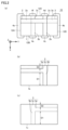
- Fig. 1 is a perspective view of a coil component 10 according to the first embodiment.
- Fig. 2 is a schematic diagram of the coil component 10 according to the first embodiment.
- Fig. 3 is a circuit diagram of a filter circuit 100 including the coil component 10 according to the first embodiment. Note that, with respect to the X-axis, Y-axis, and Z-axis defined in Fig. 1, the X-axis direction represents the front-rear direction of the coil component 10, the Y-axis direction represents the left-right direction of the coil component 10, and the Z-axis direction represents the up-down direction of the coil component 10, respectively.
- the coil component 10 is, for example, a transformer coil mounted in a filter circuit 100 used to reduce noise in a power line. As described below, the coil component 10 magnetically couples two coils to cancel the parasitic inductance of a capacitor mounted in the filter circuit 100.
- the coil component 10 is a rectangular parallelepiped chip component in which two coils are stacked in the Z direction.
- the coil component 10 is composed of an insulator 1 (housing) in which multiple insulating substrates (insulator layers) on which coil conductor patterns are formed are stacked.
- the insulating substrates are stacked in the Z direction, with the arrow pointing in the upward direction.
- the insulating substrates are made of materials such as insulating materials whose main component is borosilicate glass, or insulating resins such as alumina, zirconia, and polyimide resin.
- the interfaces between the multiple insulating substrates may not be clear due to processes such as firing and hardening.
- the insulator 1 has a pair of first and second principal surfaces 11A and 11B that face each other, and four side surfaces (first side surface 12A, second side surface 12B, third side surface 12C, and fourth side surface 12D) that connect the first principal surface 11A and the second principal surface 11B.
- the first principal surface 11A is also called the top surface
- the second principal surface 11B is also called the bottom surface.
- the coil component 10 has an external electrode 4a (first external electrode) arranged on the first side surface 12A, an external electrode 4c (second external electrode) and an external electrode 4e (fifth external electrode) arranged on the second side surface 12B, an external electrode 4d (third external electrode) and an external electrode 4f (sixth external electrode) arranged on the third side surface 12C, and an external electrode 4b (fourth external electrode) arranged on the fourth side surface 12D.
- the external electrodes 4a to 4f do not only form electrodes on the side surfaces of the insulator 1, but also form part of the electrodes on the top and bottom surfaces of the insulator 1.
- the coil component 10 includes two coils, a first conductor 2 which becomes the first coil L1, and a second conductor 3 which becomes the second coil L2, enclosed in an insulator 1, and the first coil L1 and the second coil L2 are magnetically coupled to form a transformer. Note that, in the first embodiment, an example of the coil component 10 in which the first coil L1 and the second coil L2 form a transformer is described, but the coil component 10 does not need to form a transformer as long as the first coil L1 and the second coil L2 are magnetically coupled.
- the first conductor 2 of the first coil L1 is electrically connected to the external electrode 4a on the first side 12A, and is further electrically connected to the external electrode 4c on the second side 12B and to the external electrode 4d on the third side 12C.
- the second conductor 3 of the second coil L2 is electrically connected to the external electrode 4b on the fourth side 12D, and is further electrically connected to the external electrode 4e on the second side 12B and to the external electrode 4f on the third side 12C.
- the first conductor 2 and the second conductor 3 are each formed on one of the multiple insulating substrates (for example, ceramic green sheets) that constitute the insulator 1.
- the first conductor 2 and the second conductor 3 are formed by printing, for example, a conductive paste (Ni paste) on the insulating substrate by a screen printing method.
- FIG. 2(a) is a diagram of the first conductor 2 and the second conductor 3 when viewed from the top side of the coil component 10 (when viewed from the direction of the first main surface 11A).
- FIG. 2(b) is a plan view of the first conductor 2 formed on the insulating substrate 1b, and FIG.
- the coil component 10 is formed by stacking and pressing multiple insulating substrates including the insulating substrate 1b and the insulating substrate 1c, sintering them, and then baking external electrodes on the side surfaces.
- the coil component 10 has external electrodes 4a and 4b provided on the short side surfaces (first side surface 12A, fourth side surface 12D) and external electrodes 4c to 4f provided on the long side surfaces (second side surface 12B, third side surface 12C).
- External electrodes 4a and 4b are provided so as to cover the entire short side surfaces, while external electrodes 4c to 4f are provided on only a portion of the long side surfaces.
- the position of external electrode 4e provided on second side surface 12B is at a position (first position) closer to the first side surface 12A
- the position of external electrode 4c provided on second side surface 12B is at a position (second position) closer to the fourth side surface 12D.
- the position of the external electrode 4f provided on the third side surface 12C is at a position (third position) closer to the first side surface 12A, and the position of the external electrode 4d provided on the third side surface 12C is at a position (fourth position) closer to the fourth side surface 12D.
- the distance from the fourth side surface 12D to the position of the external electrode 4c is approximately the same as the distance from the first side surface 12A to the position of the external electrode 4f
- the distance from the first side surface 12A to the position of the external electrode 4e is approximately the same as the distance from the fourth side surface 12D to the position of the external electrode 4d.
- the positions of the external electrode 4c and the external electrode 4e on the second side surface 12B and the positions of the external electrode 4d and the external electrode 4f on the third side surface 12C are in point-symmetric positions when viewed from the direction of the first main surface 11A. Therefore, the coil component 10 can be connected to the land electrode of the substrate even if it is rotated 180 degrees in a plane parallel to the substrate, as described below.
- the first conductor 2 is a T-shaped conductor pattern formed on the insulating substrate 1b, and includes a first conductor pattern 2a, a second conductor pattern 2b, and a third conductor pattern 2c.
- the first conductor pattern 2a is drawn out from the first side surface 12A side of the insulator 1 and is electrically connected to the external electrode 4a.
- the second conductor pattern 2b extends from the end of the first conductor pattern 2a in the direction of the second side surface 12B, is drawn out from the second side surface 12B, and is electrically connected to the external electrode 4c.
- the third conductor pattern 2c extends from the end of the first conductor pattern 2a in the direction of the third side surface 12C, is drawn out from the third side surface 12C, and is electrically connected to the external electrode 4d.
- the length D1 of the second conductor pattern 2b is longer than the length D2 of the third conductor pattern 2c.
- the first conductor pattern 2a is formed closer to the third side surface 12C than the second side surface 12B.
- the second conductor 3 is a T-shaped conductor pattern formed on the insulating substrate 1c as shown in FIG. 2(c), and includes a fourth conductor pattern 3a, a fifth conductor pattern 3b, and a sixth conductor pattern 3c.
- the fourth conductor pattern 3a is drawn out from the fourth side surface 12D side of the insulator 1 and is electrically connected to the external electrode 4b.
- the fifth conductor pattern 3b extends from the end of the fourth conductor pattern 3a in the direction of the second side surface 12B, is drawn out from the second side surface 12B, and is electrically connected to the external electrode 4e.
- the sixth conductor pattern 3c extends from the end of the fourth conductor pattern 3a in the direction of the third side surface 12C, is drawn out from the third side surface 12C, and is electrically connected to the external electrode 4f.
- the length D1 of the fifth conductor pattern 3b is longer than the length D2 of the sixth conductor pattern 3c.
- the fourth conductor pattern 3a is formed closer to the third side surface 12C than the second side surface 12B.
- the first conductor 2 is divided into the second conductor pattern 2b and the third conductor pattern 2c on the fourth side surface 12D side of the center of the insulating substrate 1b.
- the second conductor 3 is divided into the fifth conductor pattern 3b and the sixth conductor pattern 3c on the first side surface 12A side of the center of the insulating substrate 1c. Therefore, the second conductor pattern 2b is drawn out from a position on the second side surface 12B closer to the fourth side surface 12D than the fifth conductor pattern 3b, and the third conductor pattern 2c is drawn out from a position on the third side surface 12C closer to the fourth side surface 12D than the sixth conductor pattern 3c.
- first conductor 2a and the fourth conductor pattern 3a overlap.
- the first coil L1 (first conductor 2) and the second coil L2 (second conductor 3) are magnetically coupled by a portion of the overlapping first conductor pattern 2a and a portion of the fourth conductor pattern 3a.
- the filter circuit 100 is, for example, an EMI removal filter as shown in FIG. 3, and is a third-order T-type LC filter circuit.
- the external electrode 4a of the coil component 10 is connected to a power source (not shown), and the external electrode 4b is connected to a circuit (not shown) such as a DC/DC converter or a power supply module.
- the filter circuit 100 passes necessary components of the current flowing from the power source to the circuit, and removes unnecessary components. Specifically, a direct current is passed through the filter circuit 100, and high-frequency noise contained in the direct current is dropped to GND through the capacitor C1.
- Capacitor C1 which is a capacitance element, has its own equivalent series inductance ESL (La), which impedes the passage of high-frequency noise and degrades noise removal performance.
- This filter circuit 100 uses the negative inductance generated by the magnetic coupling of the two coils to cancel the ESL (La) of capacitor C1 and maintains high noise removal performance.
- the negative inductance generated in series with capacitor C1 is referred to as the mutual inductance M of coil component 10. As will be described later, coil component 10 can change this mutual inductance M by changing the connection path.
- the filter circuit 100 will be described using a third-order T-type LC filter circuit, but coil components of a similar configuration can also be applied to a fifth-order T-type LC filter circuit or a higher-order T-type LC filter circuit.
- the filter circuit 100 includes a capacitor C1, external electrodes 4a and 4b, an intermediate terminal T (external electrodes 4c and 4e, or external electrodes 4d and 4f), a first coil L1, and a second coil L2.
- the capacitor C1 has one end connected to the intermediate terminal T and the other end connected to the GND wiring.
- the capacitor C1 may be a multilayer ceramic capacitor mainly made of BaTiO 3 (barium titanate), a multilayer ceramic capacitor mainly made of other materials, or another type of capacitor such as an aluminum electrolytic capacitor.
- the capacitor C1 has an inductor La as a parasitic inductance (equivalent series inductance (ESL)), and is equivalent to a circuit configuration in which the inductor La is connected in series to the capacitor C1a.
- the capacitor C1 may also be equivalent to a circuit configuration in which a parasitic resistance (equivalent series resistance (ESR)) is connected in series to the inductor La and the capacitor C1a.
- the first coil L1 and the second coil L2 are connected to the intermediate terminal T.
- the first coil L1 and the second coil L2 are magnetically coupled and have a mutual inductance M.
- a negative inductance component of the same magnitude as the mutual inductance M is generated between the intermediate terminal T and the capacitor C1. This negative inductance component can be used to cancel out the parasitic inductance (inductor La) of the capacitor C1, making the parasitic inductance component of the capacitor C1 appear smaller.
- the filter circuit 100 which is composed of the capacitor C1, the first coil L1, and the second coil L2, can cancel out the parasitic inductance of the capacitor C1 with the negative inductance component due to the mutual inductance M between the first coil L1 and the second coil L2, thereby suppressing the decrease in the noise suppression effect in the high frequency band due to the parasitic inductance of the capacitor C1, and improving the noise suppression effect of the filter circuit 100.
- the value of the parasitic inductance occurring in the filter circuit 100 changes depending on the capacitor C1 and board wiring used. Therefore, in order to determine the optimal mutual inductance M for canceling out the parasitic inductance occurring in the filter circuit 100, it was necessary to prepare and test coil components with different mutual inductances M. Therefore, by adopting the configuration described above for the coil component 10, different mutual inductances M can be generated simply by changing the connection path, reducing the number of coil components required for testing.
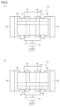
- FIG. 4 is a schematic diagram for explaining the connection path between the coil component 10 according to the first embodiment and the land electrodes 5a to 5e of the substrate.
- the coil component 10 connects the external electrode 4a to the land electrode 5a, connects the external electrode 4b to the land electrode 5b, connects the external electrodes 4c and 4e to the land electrode 5c, connects the external electrode 4d to the land electrode 5d, and connects the external electrode 4f to the land electrode 5e.
- the land electrode 5c electrically connects the external electrode 4c to the external electrode 4e
- the external electrodes 4c and 4e are electrically connected to the capacitor C1 as intermediate terminals T by electrically connecting the external electrodes 4c and 4e to the external electrode 4c.
- FIG. 4(a) shows only the land electrodes 5a to 5e, and does not show the substrate on which the land electrodes 5a to 5e are provided.
- FIG. 4(b) illustrates a connection path of the coil component 10 that is different from the connection path of the coil component 10 shown in FIG. 4(a).
- the connection path of the coil component 10 shown in FIG. 4(b) is a connection path in which the coil component 10 is rotated 180 degrees in a plane parallel to the substrate with respect to FIG. 4(a) and connected to the land electrodes 5a to 5e of the substrate. As shown in FIG.
- the coil component 10 connects the external electrode 4a to the land electrode 5b, connects the external electrode 4b to the land electrode 5a, connects the external electrodes 4d and 4f to the land electrode 5c, connects the external electrode 4e to the land electrode 5d, and connects the external electrode 4d to the land electrode 5e.
- the external electrodes 4d and 4f are electrically connected to the capacitor C1 as intermediate terminals T by electrically connecting the external electrodes 4d and 4f to the land electrode 5c.
- FIG. 4(b) only the land electrodes 5a to 5e are shown, and the substrate on which the land electrodes 5a to 5e are provided is not shown.
- the effective magnetic coupling portion K in the coil component 10 is the portion where a part of the first conductor pattern 2a overlaps a part of the fourth conductor pattern 3a.
- the path from the magnetic coupling portion K to the external electrodes 4c, 4e, which are the intermediate terminals T becomes a parasitic inductance.
- the path from the magnetic coupling portion K to the external electrodes 4d, 4f, which are the intermediate terminals T becomes a parasitic inductance.
- the length D1 of the second conductor pattern 2b and the fifth conductor pattern 3b is longer than the length D2 of the third conductor pattern 2c and the sixth conductor pattern 3c, so the parasitic inductance of the second conductor pattern 2b and the fifth conductor pattern 3b is greater than the parasitic inductance of the third conductor pattern 2c and the sixth conductor pattern 3c.
- the mutual inductance M when the coil component 10 is connected to the land electrodes 5a to 5e via the connection path shown in Figure 4(a) is greater than the mutual inductance M when the coil component 10 is connected to the land electrodes 5a to 5e via the connection path shown in Figure 4(b) (the absolute value of the mutual inductance M is smaller).
- the element size of the coil component 10 used in the simulation is 2.5 mm ⁇ 2.0 mm ⁇ 0.9 mm
- the width of each conductor pattern is 0.2 mm
- the distance between the second conductor pattern 2b and the fifth conductor pattern 3b in top view is 0.6 mm
- the length D1 is 0.5 mm
- the length D2 is 1.3 mm
- the interlayer distance between the first coil L1 and the second coil L2 is 0.21 mm.
- the mutual inductance M can be changed by 0.15 nH (about 14%) just by changing the connection path of the coil component 10.
- Figure 5 is a schematic diagram for explaining another connection path between the coil component 10 according to the first embodiment and the land electrodes of the substrate.
- the coil component 10 connects the external electrode 4a to the land electrode 5a, connects the external electrode 4b to the land electrode 5b, connects the external electrodes 4c and 4e to the land electrode 5c, and connects the external electrodes 4d and 4f to the land electrode 5f.
- the land electrode 5c electrically connects the external electrodes 4c and 4e to the external electrode 4c, electrically connecting the external electrodes 4c and 4e to the capacitor C1 as intermediate terminals T, and electrically connecting the external electrodes 4d and 4f to the land electrode 5f.
- the coil component 10 connects the external electrode 4a to the land electrode 5b, connects the external electrode 4b to the land electrode 5a, connects the external electrodes 4c and 4e to the land electrode 5f, and connects the external electrodes 4d and 4f to the land electrode 5c.
- the land electrode 5c electrically connects the external electrodes 4d and 4f to the capacitor C1 as the intermediate terminal T by electrically connecting the external electrodes 4d and 4f to the external electrode 4c
- the land electrode 5f electrically connects the external electrodes 4c and 4e.
- a path of the second conductor pattern 2b-external electrode 4c-land electrode 5f-external electrode 4e-fifth conductor pattern 3b is added to the connection path shown in FIG. 4(b).
- FIG. 6 is a schematic diagram for explaining yet another connection path between the coil component 10 according to the first embodiment and the land electrodes of the substrate.
- the coil component 10 connects the external electrode 4a to the land electrode 5a, connects the external electrode 4b to the land electrode 5b, connects the external electrodes 4c and 4e to the land electrode 5c, connects the external electrodes 4d and 4f to the land electrode 5f, and electrically connects the land electrode 5c to the land electrode 5f with the wiring 6.
- the wiring 6 electrically connects the land electrode 5c to the land electrode 5f, so that the external electrodes 4c to 4f are electrically connected to the capacitor C1 as the intermediate terminal T.
- Fig. 6(b) is a circuit diagram of a filter circuit 100a including a coil component 10 mounted on a substrate with the connection path shown in Fig. 6(a).
- the filter circuit 100a is a circuit in which a coil L1a formed by the first conductor pattern 2a and the second conductor pattern 2b, a coil L1b formed by the first conductor pattern 2a and the third conductor pattern 2c, a coil L2a formed by the fourth conductor pattern 3a and the fifth conductor pattern 3b, and a coil L2b formed by the fourth conductor pattern 3a and the sixth conductor pattern 3c are electrically connected by wiring 6.
- the wiring 6 is formed with a width of 1.1 mm, which is the same width as the land electrodes 5c and 5f, but this width may be narrower.
- the mutual inductance M can be increased by narrowing the width of the wiring 6.
- FIG. 7 is a schematic diagram of a coil component 10A according to the second embodiment. Note that in the coil component 10A shown in the second embodiment, the same components as those in the coil component 10 according to the first embodiment are designated by the same reference numerals and will not be described in detail again. Also, the coil component 10A shown in the second embodiment can be applied to the filter circuit 100 according to the first embodiment in place of the coil component 10 according to the first embodiment.
- the coil component 10A includes two coils, a first conductor 21 which becomes the first coil L1 and a second conductor 31 which becomes the second coil L2, in an insulator 1, and the first coil L1 and the second coil L2 are magnetically coupled to form a transformer.
- FIG. 7(a) is a diagram of the first conductor 21 and the second conductor 31 when viewed from the top side of the coil component 10A.
- FIG. 7(b) is a plan view of the first conductor 21 formed on the insulating substrate 1b
- FIG. 7(c) is a plan view of the second conductor 31 formed on the insulating substrate 1c.
- the coil component 10A is formed by stacking and crimping a plurality of insulating substrates including the insulating substrate 1b and the insulating substrate 1c, sintering them, and then baking external electrodes onto the side surfaces.
- the first conductor 21 is a conductor pattern formed on the insulating substrate 1b by combining a T-shape and an L-shape, as shown in FIG. 7(b), and includes a first conductor pattern 21a, a second conductor pattern 21b, and a third conductor pattern 21c.
- the first conductor pattern 21a is drawn out from the first side surface 12A side of the insulator 1 and is electrically connected to the external electrode 4a.
- the second conductor pattern 21b includes a conductor pattern 21b1 extending from the end of the first conductor pattern 21a in the direction of the second side surface 12B, a conductor pattern 21b2 extending in the direction of the first side surface 12A, and a conductor pattern 21b3 drawn out from the second side surface 12B and electrically connected to the external electrode 4e.
- the third conductor pattern 21c extends from the end of the first conductor pattern 21a in the direction of the third side surface 12C, and is drawn out from the third side surface 12C and electrically connected to the external electrode 4d.
- the first conductor 21 forms a T-shape with the first conductor pattern 21a, conductor pattern 21b1, and third conductor pattern 21c, and an L-shape with the conductor pattern 21b2 and conductor pattern 21b3.
- the first conductor 21 has a conductor pattern 21b2 that is folded back in the direction of the first side surface 12A on the second conductor pattern 21b.
- the second conductor pattern 21b is longer than the third conductor pattern 21c.
- the second conductor 31 is a conductor pattern formed on the insulating substrate 1c by combining a T-shape and an L-shape, as shown in FIG. 7(c), and includes a fourth conductor pattern 31a, a fifth conductor pattern 31b, and a sixth conductor pattern 31c.
- the fourth conductor pattern 31a is drawn out from the fourth side surface 12D side of the insulator 1 and is electrically connected to the external electrode 4b.
- the fifth conductor pattern 31b includes a conductor pattern 31b1 extending from the end of the fourth conductor pattern 31a in the direction of the second side surface 12B, a conductor pattern 31b2 extending in the direction of the fourth side surface 12D, and a conductor pattern 31b3 drawn out from the second side surface 12B and electrically connected to the external electrode 4c.
- the sixth conductor pattern 31c extends from the end of the fourth conductor pattern 31a in the direction of the third side surface 12C, and is drawn out from the third side surface 12C and electrically connected to the external electrode 4f.
- the second conductor 31 forms a T-shape with the fourth conductor pattern 31a, conductor pattern 31b1, and sixth conductor pattern 31c, and an L-shape with conductor patterns 31b2 and conductor pattern 31b3.
- the second conductor 31 has a conductor pattern 31b2 that is folded back in the direction of the fourth side surface 12D on the fifth conductor pattern 31b.
- the fifth conductor pattern 31b is longer than the sixth conductor pattern 31c.
- conductor pattern 21b2 is provided on second conductor pattern 21b that folds back in the direction of first side surface 12A
- conductor pattern 31b2 is provided on fifth conductor pattern 31b that folds back in the direction of fourth side surface 12D, so that conductor patterns 21b2 and 31b2 overlap when viewed in a plan view from the top surface.
- the connection path shown in FIG. 7(a) has a mutual inductance M that is smaller by 0.09 nH than the connection path shown in FIG. 4(a).
- the coil component 10A may be configured to have an overlapping portion between the third conductor pattern 21c and the sixth conductor pattern 31c, instead of having an overlapping portion between the second conductor pattern 21b and the fifth conductor pattern 31b.
- the third conductor pattern 21c includes a conductor pattern extending from an end of the first conductor pattern 21a in the direction of the third side surface 12C, a conductor pattern extending in the direction of the first side surface 12A, and a conductor pattern drawn from the third side surface 12C and electrically connected to the external electrode 4f.
- the sixth conductor pattern 31c includes a conductor pattern extending from an end of the fourth conductor pattern 31a in the direction of the third side surface 12C, a conductor pattern extending in the direction of the fourth side surface 12D, and a conductor pattern drawn from the third side surface 12C and electrically connected to the external electrode 4d.
- FIG. 8 is a schematic diagram of a coil component 10B according to the third embodiment. Note that in the coil component 10B shown in the third embodiment, the same reference numerals are used for the same configuration as the coil component 10 according to the first embodiment, and detailed description will not be repeated. Also, the coil component 10B shown in the third embodiment can be applied to the filter circuit 100 according to the first embodiment in place of the coil component 10 according to the first embodiment.
- the coil component 10B includes two coils, a first conductor 22 which becomes the first coil L1 and a second conductor 32 which becomes the second coil L2, in an insulator 1, and the first coil L1 and the second coil L2 are magnetically coupled to form a transformer.
- FIG. 8(a) is a diagram of the first conductor 22 and the second conductor 32 when viewed from the top side of the coil component 10B.
- FIG. 8(b) is a plan view of the first conductor 22 formed on the insulating substrate 1b
- FIG. 8(c) is a plan view of the second conductor 32 formed on the insulating substrate 1c.
- the coil component 10B is formed by stacking and crimping a plurality of insulating substrates including the insulating substrate 1b and the insulating substrate 1c, sintering them, and then baking external electrodes onto the side surfaces.
- the first conductor 22 is a conductor pattern formed by combining two L-shaped shapes formed on the insulating substrate 1b, and includes a first conductor pattern 22a, a second conductor pattern 22b, and a third conductor pattern 22c.
- the first conductor pattern 22a is drawn out from the first side surface 12A side of the insulator 1 and is electrically connected to the external electrode 4a.
- the second conductor pattern 22b extends from the end of the first conductor pattern 22a in the direction of the second side surface 12B, is drawn out from the second side surface 12B, and is electrically connected to the external electrode 4c.
- the third conductor pattern 22c extends from the middle of the first conductor pattern 22a in the direction of the third side surface 12C, is drawn out from the third side surface 12C, and is electrically connected to the external electrode 4f.
- the first conductor 22 forms an L-shape with the first conductor pattern 22a and the second conductor pattern 22b, and also forms an L-shape with the first conductor pattern 22a and the third conductor pattern 22c. Note that the second conductor pattern 22b is longer than the third conductor pattern 22c.
- the second conductor 32 is a conductor pattern that combines two L-shaped shapes formed on the insulating substrate 1c, and includes a fourth conductor pattern 32a, a fifth conductor pattern 32b, and a sixth conductor pattern 32c.
- the fourth conductor pattern 32a is drawn out from the fourth side surface 12D side of the insulator 1 and is electrically connected to the external electrode 4b.
- the fifth conductor pattern 32b extends from an end of the fourth conductor pattern 32a in the direction of the second side surface 12B, is drawn out from the second side surface 12B, and is electrically connected to the external electrode 4e.
- the sixth conductor pattern 32c extends from the middle of the fourth conductor pattern 32a in the direction of the third side surface 12C, is drawn out from the third side surface 12C, and is electrically connected to the external electrode 4d.
- the second conductor 32 forms an L-shape with the fourth conductor pattern 32a and the fifth conductor pattern 32b, and also forms an L-shape with the fourth conductor pattern 32a and the sixth conductor pattern 32c.
- the fifth conductor pattern 32b is longer than the sixth conductor pattern 32c.
- FIG. 9 is a schematic diagram for explaining the connection path between the coil component 10B according to the third embodiment and the land electrodes 5a to 5e of the substrate.
- the coil component 10B connects the external electrode 4a to the land electrode 5a, connects the external electrode 4b to the land electrode 5b, connects the external electrodes 4c and 4e to the land electrode 5c, connects the external electrode 4d to the land electrode 5d, and connects the external electrode 4f to the land electrode 5e.
- the external electrode 4c is electrically connected to the external electrode 4e by the land electrode 5c, and the external electrodes 4c and 4e are electrically connected to the capacitor C1 as intermediate terminals T.
- FIG. 9(a) shows only the land electrodes 5a to 5e, and does not show the substrate on which the land electrodes 5a to 5e are provided.
- FIG. 9(b) shows a connection path of the coil component 10B that is different from the connection path of the coil component 10B shown in FIG. 9(a).
- the connection path of the coil component 10B shown in FIG. 9(b) is a connection path that rotates the coil component 10B 180 degrees in a plane parallel to the substrate with respect to FIG. 9(a) and connects it to the land electrodes 5a to 5e of the substrate. As shown in FIG.
- the coil component 10B connects the external electrode 4a to the land electrode 5b, connects the external electrode 4b to the land electrode 5a, connects the external electrodes 4d and 4f to the land electrode 5c, connects the external electrode 4e to the land electrode 5d, and connects the external electrode 4c to the land electrode 5e.
- the external electrode 4d is electrically connected to the external electrode 4f by the land electrode 5c, and the external electrodes 4d and 4f are electrically connected to the capacitor C1 as intermediate terminals T.
- FIG. 9(b) only the land electrodes 5a to 5e are shown, and the substrate on which the land electrodes 5a to 5e are provided is not shown.
- the portion where a part of the first conductor pattern 2a overlaps a part of the fourth conductor pattern 3a does not become an effective magnetic coupling portion K, and the current only detouring flows through the path I of the sixth conductor pattern 32c-external electrode 4d-land electrode 5c-external electrode 4f-third conductor pattern 22c. Therefore, in the connection path of the coil component 10B shown in FIG. 9(b), there is no effective magnetic coupling portion K, and the value of the mutual inductance M of the coil component 10B is 0 (zero).
- coil component 10B has second conductor pattern 22b extending from the end of first conductor pattern 22a in the direction of second side surface 12B, third conductor pattern 22c extending from the middle of first conductor pattern 22a in the direction of third side surface 12C, fifth conductor pattern 32b extending from the end of fourth conductor pattern 32a in the direction of second side surface 12B, and sixth conductor pattern 32c extending from the middle of fourth conductor pattern 32a in the direction of third side surface 12C.
- the coil component 10B may have the second conductor pattern 22b extending from the middle of the first conductor pattern 22a toward the second side surface 12B, the third conductor pattern 22c extending from the end of the first conductor pattern 22a toward the third side surface 12C, the fifth conductor pattern 32b extending from the middle of the fourth conductor pattern 32a toward the second side surface 12B, and the sixth conductor pattern 32c extending from the end of the fourth conductor pattern 32a toward the third side surface 12C.
- the mutual inductance M of the path on one side it is possible to compare the noise suppression effect due to the mutual inductance M, or by forming multiple land electrodes on the substrate on which the coil component 10B is mounted, the mutual inductance M can be generated only in places where the noise suppression effect is high, and the value of the mutual inductance M can be set to zero in other parts.
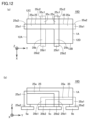
- FIG. 10 is a schematic diagram of a coil component 10C according to the fourth embodiment. Note that in the coil component 10C shown in the fourth embodiment, the same components as those in the coil component 10 according to the first embodiment are designated by the same reference numerals and will not be described in detail again. Also, the coil component 10C shown in the fourth embodiment can be applied to the filter circuit 100 according to the first embodiment in place of the coil component 10 according to the first embodiment.
- Coil component 10C includes two layers of first conductors 23 and 24 that form first coil L1, and two layers of second conductors 33 and 34 that form second coil L2, enclosed in insulator 1, with first coil L1 and second coil L2 magnetically coupling to form a transformer.
- Figure 10(a) is a diagram of first conductors 23, 24 and second conductors 33, 34 when viewed from above the top surface of coil component 10C.
- Figure 10(b) is a side view of coil component 10C.
- the first conductor 23 and the first conductor 24 are stacked in the Z direction as shown in FIG. 10(b) and are electrically connected by via conductors 51.
- the first conductor 23 includes a conductor pattern that is drawn out from the first side surface 12A of the insulator 1 and is electrically connected to the external electrode 4a, and a conductor pattern that is drawn out from the third side surface 12C and is electrically connected to the external electrode 4d.
- the first conductor 24 includes a conductor pattern that is drawn out from the second side surface 12B and is electrically connected to the external electrode 4c.
- the second conductor 33 and the second conductor 34 are stacked in the Z direction as shown in FIG. 10(b) and are electrically connected by via conductors 52.
- the second conductor 33 includes a conductor pattern that is drawn out from the fourth side surface 12D of the insulator 1 and is electrically connected to the external electrode 4b, and a conductor pattern that is drawn out from the third side surface 12C and is electrically connected to the external electrode 4f.
- the second conductor 34 includes a conductor pattern that is drawn out from the second side surface 12B and is electrically connected to the external electrode 4e.
- FIG. 11 is an exploded plan view showing the configuration of coil component 10C according to embodiment 4.
- Coil component 10C is formed by stacking multiple insulating substrates including insulating substrates 1a to 1d on which coil conductors are formed as shown in FIGS. 11(a) to 11(d) to form insulator 1.
- FIG. 11(a) is a plan view of first conductor 23 formed on insulating substrate 1a
- FIG. 11(b) is a plan view of first conductor 24 formed on insulating substrate 1b
- FIG. 11(c) is a plan view of second conductor 34 formed on insulating substrate 1c
- FIG. 11(d) is a plan view of second conductor 33 formed on insulating substrate 1d.
- Coil component 10C is formed by stacking multiple insulating substrates including insulating substrates 1a to 1d, pressing them together, firing them, and then baking external electrodes onto the sides.
- the insulating substrate 1a is provided with the conductor patterns 23a-23d of the first conductor 23 constituting the first coil L1.
- the conductor pattern 23a is drawn out from the first side surface 12A of the insulator 1 shown in FIG. 10(a) and is electrically connected to the external electrode 4a.
- the conductor pattern 23b extends from the end of the conductor pattern 23a in the direction of the second side surface 12B.
- the conductor pattern 23c extends from the end of the conductor pattern 23a in the direction of the third side surface 12C, and is drawn out from the third side surface 12C and electrically connected to the external electrode 4d.
- the conductor pattern 23d extends from the end of the conductor pattern 23b in the direction of the first side surface 12A.
- the end of the conductor pattern 23d is provided with a connection portion 23A that connects to the via conductor 51.
- conductor patterns 24a-24d of the first conductor 24 constituting the first coil L1 are formed on the insulating substrate 1b.
- the conductor pattern 24a extends in the direction of the first side surface 12A of the insulator 1 shown in FIG. 10(a).
- a connection portion 24A that connects to the via conductor 51 is provided at the end of the conductor pattern 24a.
- the conductor pattern 24b extends from the end of the conductor pattern 24a in the direction of the third side surface 12C.
- the conductor pattern 24c extends from the end of the conductor pattern 24b in the direction of the fourth side surface 12D.
- the conductor pattern 24d extends from the end of the conductor pattern 24c in the direction of the second side surface 12B, and is drawn out from the second side surface 12B to be electrically connected to the external electrode 4c.
- conductor patterns 34a-34d of the second conductor 34 constituting the second coil L2 are formed on the insulating substrate 1c.
- the conductor pattern 34a extends in the direction of the fourth side surface 12D of the insulator 1 shown in FIG. 10(a).
- a connection portion 34A that connects to the via conductor 52 is provided at the end of the conductor pattern 34a.
- the conductor pattern 34b extends from the end of the conductor pattern 34a in the direction of the third side surface 12C.
- the conductor pattern 34c extends from the end of the conductor pattern 34b in the direction of the first side surface 12A.
- the conductor pattern 34d extends from the end of the conductor pattern 34c in the direction of the second side surface 12B, and is drawn out from the second side surface 12B to be electrically connected to the external electrode 4e.
- the conductor patterns 33a to 33d of the second conductor 33 constituting the second coil L2 are formed on the insulating substrate 1d as shown in FIG. 11(d).
- the conductor pattern 33a is drawn out from the fourth side surface 12D side of the insulator 1 shown in FIG. 10(a) and is electrically connected to the external electrode 4b.
- the conductor pattern 33b extends from the end of the conductor pattern 33a in the direction of the second side surface 12B.
- the conductor pattern 33c extends from the end of the conductor pattern 33a in the direction of the third side surface 12C, and is drawn out from the third side surface 12C and electrically connected to the external electrode 4f.
- the conductor pattern 33d extends from the end of the conductor pattern 33b in the direction of the fourth side surface 12D.
- the end of the conductor pattern 33d is provided with a connection portion 33A that connects to the via conductor 52.
- coil component 10C when viewed in plan from the top surface, the area where parts of first conductors 23, 24 overlap parts of second conductors 33, 34 is greater than in coil component 10, and the effective magnetic coupling parts are therefore greater.
- the value of mutual inductance M is smaller (the absolute value of mutual inductance M is larger) due to the increased effective magnetic coupling parts.
- FIG. 12 is a schematic diagram of a coil component 10D according to the fifth embodiment. Note that in the coil component 10D shown in the fifth embodiment, the same components as those in the coil component 10 according to the first embodiment are denoted by the same reference numerals, and detailed description thereof will not be repeated. Also, the coil component 10D shown in the fifth embodiment can be applied to the filter circuit 100 according to the first embodiment in place of the coil component 10 according to the first embodiment.
- FIG. 12(a) is a diagram of the first conductor 25 and the second conductor 35 when viewed from the top surface side of the coil component 10D.
- FIG. 12(b) is a side view of the coil component 10D.
- the first conductor 25 is formed of a metal plate integrally with the first conductor pattern 25a, the second conductor pattern 25b, and the third conductor pattern 25c that form the first coil L1, and the lead wires 25a1, 25b1, and 25c1 that are drawn out from the housing 1A.
- the second conductor 35 is formed of a metal plate integrally with the fourth conductor pattern 35a, the fifth conductor pattern 35b, and the sixth conductor pattern 35c that form the second coil L2, and the lead wires 35a1, 35b1, and 35c1 that are drawn out from the housing 1A.
- Coil component 10D contains two coils in housing 1A: a part of first conductor 25 that becomes first coil L1, and a part of second conductor 35 that becomes second coil L2, and first coil L1 and second coil L2 are magnetically coupled to form a transformer.
- first coil L1 and second coil L2 which are made of conductors, are fixed with the molded resin of housing 1A at a position where they overlap, and lead wires 25a1, 25b1, 25c1, 35a1, 35b1, and 35c1 drawn from the side of housing 1A are bent along the side of housing 1A.
- the ends of the lead wires 25a1, 25b1, 25c1, 35a1, 35b1, and 35c1 are bent to the bottom surface of the housing 1A to form external electrodes 25a2, 25b2, 25c2, 35a2, 35b2, and 35c2 for electrical connection to the land electrodes 5a to 5e.
- the external electrode 25a2 corresponds to the external electrode 4a of the coil component 10
- the external electrode 25b2 corresponds to the external electrode 4c of the coil component 10
- the external electrode 25c2 corresponds to the external electrode 4d of the coil component 10
- the external electrode 35a2 corresponds to the external electrode 4b of the coil component 10
- the external electrode 35b2 corresponds to the external electrode 4e of the coil component 10
- the external electrode 35c2 corresponds to the external electrode 4f of the coil component 10.
- the housing 1A has short side surfaces (first side surface 12A, fourth side surface 12D) and long side surfaces (second side surface 12B, third side surface 12C).
- first side surface 12A fourth side surface 12D
- second side surface 12B third side surface 12C
- first position the side closer to the first side surface 12A
- fourth side surface 12D the second position
- second position the side closer to the fourth side surface 12D
- the third side surface 12C the side closer to the first side surface 12A is defined as the third position
- the side closer to the fourth side surface 12D is defined as the fourth position.
- the first conductor 25 includes a first conductor pattern 25a, a second conductor pattern 25b, and a third conductor pattern 25c, which are T-shaped conductor patterns.
- the first conductor pattern 25a is drawn out from the first side surface 12A side of the housing 1A, and leads to a lead wire 25a1 and an external electrode 25a2.
- the second conductor pattern 25b extends from an end of the first conductor pattern 25a in the direction of the second side surface 12B, and is drawn out from a second position on the second side surface 12B to lead wire 25b1 and an external electrode 25b2.
- the third conductor pattern 25c extends from an end of the first conductor pattern 25a in the direction of the third side surface 12C, and is drawn out from a fourth position on the third side surface 12C to lead wire 25c1 and an external electrode 25c2.
- the second conductor pattern 25b is longer than the third conductor pattern 25c.
- the second conductor 35 includes a fourth conductor pattern 35a, a fifth conductor pattern 35b, and a sixth conductor pattern 35c, which are T-shaped conductor patterns.
- the fourth conductor pattern 35a is drawn out from the fourth side surface 12D side of the housing 1A, and leads to a drawn-out wire 35a1 and an external electrode 35a2.
- the fifth conductor pattern 35b extends from an end of the fourth conductor pattern 35a in the direction of the second side surface 12B, and is drawn out from a first position on the second side surface 12B, and leads to a drawn-out wire 35b1 and an external electrode 35b2.
- the sixth conductor pattern 35c extends from an end of the fourth conductor pattern 35a in the direction of the third side surface 12C, and is drawn out from a third position on the third side surface 12C, and leads to a drawn-out wire 35c1 and an external electrode 35c2.
- the fifth conductor pattern 35b is longer than the sixth conductor pattern 35c.
- the first conductor 25 and the second conductor 35 are formed from a metal plate or metal wire, so that the thickness of the first conductor 25 and the second conductor 35 can be increased, thereby reducing the DC resistance and increasing the rated current.
- the first conductor 25 and the second conductor 35 are described as including a T-shaped conductor pattern, but the configurations described in the second to fourth embodiments may also be adopted.
- FIG. 12 shows an example in which the external electrodes 25a2, 25b2, etc. are linear extensions of the lead wires 25a1, 25b1, etc.
- the shapes of the external electrodes 25a2, 25b2, etc. are not limited to this, and the external electrodes 25a2, 25b2, etc. may be folded toward the underside of the housing 1A so that a part of the external electrodes 25a2, 25b2, etc. is parallel to the land electrodes 5a, 5b, etc.
- the housing of the coil components 10, 10A to 10D is made of, for example, an insulating material mainly composed of borosilicate glass, or an insulating resin such as alumina, zirconia, or polyimide resin.
- the housing of the coil components 10, 10A to 10D may be made of a magnetic material or a dielectric material.
- the housing of the coil components 10, 10A to 10D may be made of, for example, a magnetic material such as ferrite.
- the housing of the coil components 10, 10A to 10D may be made of, for example, titanium oxide or barium oxide. Insulating materials containing these magnetic materials or dielectric materials may also be used.
- the second conductor pattern 2b, 21b to 25b is longer than the third conductor pattern 2c, 21c to 25c
- the fifth conductor pattern 3b, 31b to 35b is longer than the sixth conductor pattern 3c, 31c to 35c.
- the coil components may have the second conductor pattern 2b, 21b to 25b shorter in length than the third conductor pattern 2c, 21c to 25c, and the fifth conductor pattern 3b, 31b to 35b shorter in length than the sixth conductor pattern 3c, 31c to 35c.
- the value of mutual inductance M of coil components 10, 10A-10D can be changed by changing the ratio of the length between the second conductor pattern 2b, 21b-25b and the third conductor pattern 2c, 21c-25c, and the ratio of the length between the fifth conductor pattern 3b, 31b-35b and the sixth conductor pattern 3c, 31c-35c when viewed in a plan view from the top side.
- the position of the external electrode 4c (second position) and the position of the external electrode 4e (first position) on the second side surface 12B, and the position of the external electrode 4d (fourth position) and the position of the external electrode 4f (third position) on the third side surface 12C have been described as being point-symmetrical when viewed from the direction of the first main surface 11A.
- the external electrodes 4c to 4f when the external electrodes 4c to 4f are formed on the sides of the insulator 1 as well as on the top and bottom surfaces, even if the coil components are rotated 180 degrees in a plane parallel to the substrate, they can be turned over and connected to the land electrodes of the substrate without being connected to the land electrodes of the substrate.
- a coil component includes a housing having a pair of first and second main surfaces opposed to each other and four side surfaces connecting the first and second main surfaces; A first coil disposed inside the housing; a second coil magnetically coupled to the first coil,
- the first coil is a first conductor pattern extending from a first side surface of the housing; a second conductor pattern extending from the first conductor pattern in a direction toward the second side surface; a third conductor pattern extending from the first conductor pattern in a direction toward a third side surface opposed to the second side surface,
- the second coil is a fourth conductor pattern extended from a fourth side surface of the housing opposite to the first side surface; a fifth conductor pattern extending from the second conductor pattern in a direction toward the second side surface; a sixth conductor pattern extending from the second conductor pattern in a direction toward the third side surface, the second conductor pattern is drawn out from a position on the second side face closer to the fourth side face than the fifth conductor pattern;
- the third conductor pattern is led
- the second conductor pattern has a different length from the third conductor pattern when viewed from the first principal surface;
- the fifth conductor pattern has a different length from the sixth conductor pattern when viewed from the first main surface.
- the coil component according to (2), The first conductor pattern and the fourth conductor pattern are disposed on the second side surface side when viewed from the first main surface direction.
- a side closer to the first side surface is defined as a first position, and a side closer to the fourth side surface is defined as a second position;
- a side closer to the first side surface is defined as a third position, and a side closer to the fourth side surface is defined as a fourth position;
- a second conductor pattern is extended from the second location;
- a third conductor pattern is led out from a fourth location;
- a fifth conductor pattern is extended from the first location;
- a sixth conductor pattern is extended from the third location.
- a side closer to the first side surface is defined as a first position, and a side closer to the fourth side surface is defined as a second position;
- a side closer to the first side surface is defined as a third position, and a side closer to the fourth side surface is defined as a fourth position;
- the second conductor pattern is drawn out from the first position, the third conductor pattern is drawn out from the fourth position, the fifth conductor pattern is drawn out from the second position, and the sixth conductor pattern is drawn out from the third position.
- the second conductor pattern is drawn out from the second position, the third conductor pattern is drawn out from the third position, the fifth conductor pattern is drawn out from the first position, and the sixth conductor pattern is drawn out from the fourth position.
- the coil component according to any one of (4) to (6), The first position and the second position on the second side surface and the third position and the fourth position on the third side surface are located at positions that are point-symmetric when viewed from the direction of the first main surface.
- the coil component according to any one of (1) to (7), The second conductor pattern, the third conductor pattern, the fifth conductor pattern, and the sixth conductor pattern are electrically connected by wiring.
- the coil component according to any one of (1) to (8),
- the housing is made of a dielectric material.
- the housing is an insulator in which a plurality of insulating substrates, each having a plurality of conductor patterns formed thereon, are laminated in a direction from the second principal surface to the first principal surface; a first external electrode provided on the first side surface and electrically connected to the first conductor pattern; a second external electrode on the second side surface, the second external electrode being electrically connected to the second conductor pattern; a third external electrode provided on a third side surface and electrically connected to the third conductor pattern; a fourth external electrode provided on the fourth side surface and electrically connected to the fourth conductor pattern; a fifth external electrode on the second side surface, the fifth external electrode being electrically connected to the fifth conductor pattern; A sixth external electrode is provided on the third side surface and is electrically connected to the sixth conductor pattern.
- the coil component according to (10), The first coil and the second coil are formed by electrically connecting a plurality of laminated conductor patterns inside the housing.
- the coil component according to any one of (1) to (11), The first coil and the second coil are formed from a metal plate or a metal wire, and a part of the metal plate or the metal wire is pulled out from the side surface of the housing.
- a filter circuit includes the coil component according to any one of (1) to (12), a capacitor electrically connected to the second conductor pattern and the fifth conductor pattern of the coil component, or electrically connected to the third conductor pattern and the sixth conductor pattern of the coil component.
Landscapes
- Engineering & Computer Science (AREA)
- Power Engineering (AREA)
- Microelectronics & Electronic Packaging (AREA)
- Coils Or Transformers For Communication (AREA)
Priority Applications (1)
| Application Number | Priority Date | Filing Date | Title |
|---|---|---|---|
| JP2025501147A JPWO2024172015A1 (https=) | 2023-02-16 | 2024-02-13 |
Applications Claiming Priority (2)
| Application Number | Priority Date | Filing Date | Title |
|---|---|---|---|
| JP2023022478 | 2023-02-16 | ||
| JP2023-022478 | 2023-02-16 |
Publications (1)
| Publication Number | Publication Date |
|---|---|
| WO2024172015A1 true WO2024172015A1 (ja) | 2024-08-22 |
Family
ID=92420198
Family Applications (1)
| Application Number | Title | Priority Date | Filing Date |
|---|---|---|---|
| PCT/JP2024/004775 Ceased WO2024172015A1 (ja) | 2023-02-16 | 2024-02-13 | コイル部品、これを含むフィルタ回路 |
Country Status (2)
| Country | Link |
|---|---|
| JP (1) | JPWO2024172015A1 (https=) |
| WO (1) | WO2024172015A1 (https=) |
Citations (4)
| Publication number | Priority date | Publication date | Assignee | Title |
|---|---|---|---|---|
| JPH03274815A (ja) * | 1990-03-23 | 1991-12-05 | Murata Mfg Co Ltd | 複合積層電子部品 |
| JP2012164828A (ja) * | 2011-02-07 | 2012-08-30 | Tdk Corp | チップ電子部品、チップ電子部品の実装構造、及びスイッチング電源回路 |
| WO2020121592A1 (ja) * | 2018-12-10 | 2020-06-18 | 株式会社村田製作所 | コイル部品および、これを含むフィルタ回路 |
| WO2022014432A1 (ja) * | 2020-07-13 | 2022-01-20 | 株式会社村田製作所 | フィルタ回路および、これを含む電源装置 |
-
2024
- 2024-02-13 JP JP2025501147A patent/JPWO2024172015A1/ja active Pending
- 2024-02-13 WO PCT/JP2024/004775 patent/WO2024172015A1/ja not_active Ceased
Patent Citations (4)
| Publication number | Priority date | Publication date | Assignee | Title |
|---|---|---|---|---|
| JPH03274815A (ja) * | 1990-03-23 | 1991-12-05 | Murata Mfg Co Ltd | 複合積層電子部品 |
| JP2012164828A (ja) * | 2011-02-07 | 2012-08-30 | Tdk Corp | チップ電子部品、チップ電子部品の実装構造、及びスイッチング電源回路 |
| WO2020121592A1 (ja) * | 2018-12-10 | 2020-06-18 | 株式会社村田製作所 | コイル部品および、これを含むフィルタ回路 |
| WO2022014432A1 (ja) * | 2020-07-13 | 2022-01-20 | 株式会社村田製作所 | フィルタ回路および、これを含む電源装置 |
Also Published As
| Publication number | Publication date |
|---|---|
| JPWO2024172015A1 (https=) | 2024-08-22 |
Similar Documents
| Publication | Publication Date | Title |
|---|---|---|
| JP7238937B2 (ja) | コイル部品および、これを含むフィルタ回路 | |
| JP6332200B2 (ja) | 電子部品 | |
| US12355416B2 (en) | Coil component, filter circuit including the coil component, and electronic device | |
| JP7318815B2 (ja) | フィルタ回路および、これを含む電源装置 | |
| US20220028597A1 (en) | Circuit element | |
| US20240428985A1 (en) | Circuit device and filter circuit | |
| US11870412B2 (en) | Multilayer substrate, circuit device, and filter circuit substrate | |
| US11264162B2 (en) | Coil component and filter circuit including the coil component | |
| US10284164B2 (en) | Circuit substrate, filter circuit, and capacitance element | |
| JP7553470B2 (ja) | 回路装置、およびフィルタ回路 | |
| WO2024172015A1 (ja) | コイル部品、これを含むフィルタ回路 | |
| JP7750436B2 (ja) | コイル部品、これを含むフィルタ回路 | |
| TWI848548B (zh) | 電子零件 | |
| TWI858536B (zh) | 電子零件 | |
| JP7694825B2 (ja) | コイル部品、およびこれを含むフィルタ回路 | |
| TWI848547B (zh) | 電子零件 | |
| JP2025172409A (ja) | コイル部品および、これを含むフィルタ回路 |
Legal Events
| Date | Code | Title | Description |
|---|---|---|---|
| 121 | Ep: the epo has been informed by wipo that ep was designated in this application |
Ref document number: 24756860 Country of ref document: EP Kind code of ref document: A1 |
|
| WWE | Wipo information: entry into national phase |
Ref document number: 2025501147 Country of ref document: JP |
|
| NENP | Non-entry into the national phase |
Ref country code: DE |
|
| 122 | Ep: pct application non-entry in european phase |
Ref document number: 24756860 Country of ref document: EP Kind code of ref document: A1 |