WO2024171007A1 - 半導体装置、および表示装置 - Google Patents
半導体装置、および表示装置 Download PDFInfo
- Publication number
- WO2024171007A1 WO2024171007A1 PCT/IB2024/051188 IB2024051188W WO2024171007A1 WO 2024171007 A1 WO2024171007 A1 WO 2024171007A1 IB 2024051188 W IB2024051188 W IB 2024051188W WO 2024171007 A1 WO2024171007 A1 WO 2024171007A1
- Authority
- WO
- WIPO (PCT)
- Prior art keywords
- transistor
- wiring
- potential
- semiconductor device
- electrically connected
- Prior art date
- Legal status (The legal status is an assumption and is not a legal conclusion. Google has not performed a legal analysis and makes no representation as to the accuracy of the status listed.)
- Ceased
Links
Images






































Classifications
-
- G—PHYSICS
- G09—EDUCATION; CRYPTOGRAPHY; DISPLAY; ADVERTISING; SEALS
- G09G—ARRANGEMENTS OR CIRCUITS FOR CONTROL OF INDICATING DEVICES USING STATIC MEANS TO PRESENT VARIABLE INFORMATION
- G09G3/00—Control arrangements or circuits, of interest only in connection with visual indicators other than cathode-ray tubes
- G09G3/20—Control arrangements or circuits, of interest only in connection with visual indicators other than cathode-ray tubes for presentation of an assembly of a number of characters, e.g. a page, by composing the assembly by combination of individual elements arranged in a matrix no fixed position being assigned to or needed to be assigned to the individual characters or partial characters
-
- G—PHYSICS
- G09—EDUCATION; CRYPTOGRAPHY; DISPLAY; ADVERTISING; SEALS
- G09G—ARRANGEMENTS OR CIRCUITS FOR CONTROL OF INDICATING DEVICES USING STATIC MEANS TO PRESENT VARIABLE INFORMATION
- G09G3/00—Control arrangements or circuits, of interest only in connection with visual indicators other than cathode-ray tubes
- G09G3/20—Control arrangements or circuits, of interest only in connection with visual indicators other than cathode-ray tubes for presentation of an assembly of a number of characters, e.g. a page, by composing the assembly by combination of individual elements arranged in a matrix no fixed position being assigned to or needed to be assigned to the individual characters or partial characters
- G09G3/22—Control arrangements or circuits, of interest only in connection with visual indicators other than cathode-ray tubes for presentation of an assembly of a number of characters, e.g. a page, by composing the assembly by combination of individual elements arranged in a matrix no fixed position being assigned to or needed to be assigned to the individual characters or partial characters using controlled light sources
- G09G3/30—Control arrangements or circuits, of interest only in connection with visual indicators other than cathode-ray tubes for presentation of an assembly of a number of characters, e.g. a page, by composing the assembly by combination of individual elements arranged in a matrix no fixed position being assigned to or needed to be assigned to the individual characters or partial characters using controlled light sources using electroluminescent panels
- G09G3/32—Control arrangements or circuits, of interest only in connection with visual indicators other than cathode-ray tubes for presentation of an assembly of a number of characters, e.g. a page, by composing the assembly by combination of individual elements arranged in a matrix no fixed position being assigned to or needed to be assigned to the individual characters or partial characters using controlled light sources using electroluminescent panels semiconductive, e.g. using light-emitting diodes [LED]
- G09G3/3208—Control arrangements or circuits, of interest only in connection with visual indicators other than cathode-ray tubes for presentation of an assembly of a number of characters, e.g. a page, by composing the assembly by combination of individual elements arranged in a matrix no fixed position being assigned to or needed to be assigned to the individual characters or partial characters using controlled light sources using electroluminescent panels semiconductive, e.g. using light-emitting diodes [LED] organic, e.g. using organic light-emitting diodes [OLED]
- G09G3/3225—Control arrangements or circuits, of interest only in connection with visual indicators other than cathode-ray tubes for presentation of an assembly of a number of characters, e.g. a page, by composing the assembly by combination of individual elements arranged in a matrix no fixed position being assigned to or needed to be assigned to the individual characters or partial characters using controlled light sources using electroluminescent panels semiconductive, e.g. using light-emitting diodes [LED] organic, e.g. using organic light-emitting diodes [OLED] using an active matrix
- G09G3/3233—Control arrangements or circuits, of interest only in connection with visual indicators other than cathode-ray tubes for presentation of an assembly of a number of characters, e.g. a page, by composing the assembly by combination of individual elements arranged in a matrix no fixed position being assigned to or needed to be assigned to the individual characters or partial characters using controlled light sources using electroluminescent panels semiconductive, e.g. using light-emitting diodes [LED] organic, e.g. using organic light-emitting diodes [OLED] using an active matrix with pixel circuitry controlling the current through the light-emitting element
-
- G—PHYSICS
- G09—EDUCATION; CRYPTOGRAPHY; DISPLAY; ADVERTISING; SEALS
- G09G—ARRANGEMENTS OR CIRCUITS FOR CONTROL OF INDICATING DEVICES USING STATIC MEANS TO PRESENT VARIABLE INFORMATION
- G09G3/00—Control arrangements or circuits, of interest only in connection with visual indicators other than cathode-ray tubes
- G09G3/20—Control arrangements or circuits, of interest only in connection with visual indicators other than cathode-ray tubes for presentation of an assembly of a number of characters, e.g. a page, by composing the assembly by combination of individual elements arranged in a matrix no fixed position being assigned to or needed to be assigned to the individual characters or partial characters
- G09G3/34—Control arrangements or circuits, of interest only in connection with visual indicators other than cathode-ray tubes for presentation of an assembly of a number of characters, e.g. a page, by composing the assembly by combination of individual elements arranged in a matrix no fixed position being assigned to or needed to be assigned to the individual characters or partial characters by control of light from an independent source
- G09G3/36—Control arrangements or circuits, of interest only in connection with visual indicators other than cathode-ray tubes for presentation of an assembly of a number of characters, e.g. a page, by composing the assembly by combination of individual elements arranged in a matrix no fixed position being assigned to or needed to be assigned to the individual characters or partial characters by control of light from an independent source using liquid crystals
Definitions
- One aspect of the present invention relates to a semiconductor device and a display device.
- one aspect of the present invention is not limited to the above technical fields.
- the technical field of one aspect of the invention disclosed in this specification relates to an object, a method, a driving method, or a manufacturing method.
- one aspect of the present invention relates to a process, a machine, manufacture, or a composition of matter.
- examples of the technical field of one aspect of the present invention disclosed in this specification include semiconductor devices, display devices, light-emitting devices, power storage devices, optical devices, imaging devices, lighting devices, arithmetic devices, control devices, memory devices, input devices, output devices, input/output devices, signal processing devices, arithmetic processing devices, electronic computers, electronic devices, driving methods thereof, or manufacturing methods thereof.
- Examples of display devices that can be used include liquid crystal display devices and light-emitting devices equipped with light-emitting elements such as organic electroluminescence (EL) elements (also called OLEDs (organic light-emitting diodes)) or light-emitting diodes (LEDs: light-emitting diodes).
- EL organic electroluminescence
- LEDs light-emitting diodes
- a source follower circuit is an analog circuit for outputting an output voltage according to an input voltage.
- a bias current flows in a transistor to which a bias voltage is applied, thereby obtaining an output voltage according to the input voltage (see, for example, Patent Document 1 and Patent Document 2).
- bias current flows through a transistor to which a bias voltage is applied, resulting in high power consumption.
- One embodiment of the present invention has an object to provide a high-definition semiconductor device or display device. Alternatively, one embodiment of the present invention has an object to provide a miniaturized semiconductor device or display device. Alternatively, one embodiment of the present invention has an object to provide a semiconductor device or display device with improved display quality. Alternatively, one embodiment of the present invention has an object to provide a semiconductor device or display device with increased operating speed. Alternatively, one embodiment of the present invention has an object to provide a semiconductor device or display device with reduced power consumption. Alternatively, one embodiment of the present invention has an object to provide a highly reliable semiconductor device or display device. Alternatively, one embodiment of the present invention has an object to provide a novel semiconductor device or display device.
- one embodiment of the present invention has an object to provide a method for driving a semiconductor device or a method for driving a display device that can improve display quality.
- one embodiment of the present invention has an object to provide a method for driving a semiconductor device or a display device that can increase the operating speed.
- one embodiment of the present invention has an object to provide a method for driving a semiconductor device or a display device that can reduce power consumption.
- one object of one embodiment of the present invention is to provide a method for driving a semiconductor device or a display device that can improve reliability.
- one object of one embodiment of the present invention is to provide a novel method for driving a semiconductor device or a display device.
- One aspect of the present invention is a semiconductor device having a first transistor, a first switch, a second switch, and a signal line, where the first transistor has a function of providing an output voltage to the signal line via the first switch according to an input voltage provided to the gate, the second switch has a function of performing an initialization operation to initialize the potential of the signal line, and the first switch has a function of performing a signal output operation to provide an output voltage to the signal line.
- One aspect of the present invention is a semiconductor device having a first transistor, a second transistor, a first switch, a second switch, a first power supply line, a second power supply line, and a signal line
- the first transistor has a function of providing an output voltage to the signal line via the first switch according to an input voltage provided to the gate
- one of the source and drain of the first transistor is electrically connected to the first power supply line
- one of the source and drain of the second transistor is electrically connected to the other of the source and drain of the first transistor
- the gate and the other of the source and drain of the second transistor are electrically connected to the second power supply line
- the second switch has a function of performing an initialization operation to initialize the potential of the signal line
- the first switch has a function of performing a signal output operation to provide an output voltage to the signal line following the initialization operation.
- One aspect of the present invention is a semiconductor device having a first transistor, a second transistor, a first switch, a second switch, a first power supply line, a second power supply line, and a signal line
- the first transistor has a function of providing an output voltage to the signal line via the first switch according to an input voltage provided to the gate
- one of the source and drain of the first transistor is electrically connected to the first power supply line
- one of the source and drain of the second transistor is electrically connected to the other of the source and drain of the first transistor
- the other of the source and drain of the second transistor is electrically connected to the second power supply line
- the gate of the second transistor is electrically connected to a first capacitor that holds the threshold voltage of the second transistor
- the second switch has a function of performing an initialization operation to initialize the potential of the signal line
- the first switch has a function of performing a signal output operation to provide an output voltage to the signal line following the initialization operation.
- a semiconductor device in which the gate of the first transistor is electrically connected to one electrode of a second capacitor that holds the threshold voltage of the first transistor, and the wiring that provides the input voltage is electrically connected to the other electrode of the second capacitor.
- the first transistor and the second transistor each preferably have a semiconductor layer, and the semiconductor layer preferably has an oxide semiconductor.
- a semiconductor device in which at least a portion of the semiconductor layer is provided inside an opening formed in the insulating layer is preferred.
- One aspect of the present invention is a display device having the semiconductor device of the above aspect of the present invention and a pixel, the pixel having a third transistor, and one of the source and drain of the third transistor being electrically connected to a signal line.
- the third transistor preferably has a semiconductor layer, and the semiconductor layer preferably includes an oxide semiconductor.
- a display device in which at least a portion of the semiconductor layer is provided inside an opening formed in the insulating layer is preferred.
- One embodiment of the present invention can provide a high-definition semiconductor device or display device. Alternatively, one embodiment of the present invention can provide a miniaturized semiconductor device or display device. Alternatively, one embodiment of the present invention can provide a semiconductor device or display device with improved display quality. Alternatively, one embodiment of the present invention can provide a semiconductor device or display device with increased operating speed. Alternatively, one embodiment of the present invention can provide a semiconductor device or display device with reduced power consumption. Alternatively, one embodiment of the present invention can provide a highly reliable semiconductor device or display device. Alternatively, one embodiment of the present invention can provide a novel semiconductor device or display device. Alternatively, one embodiment of the present invention can provide a method for driving a semiconductor device or a display device with improved display quality.
- one embodiment of the present invention can provide a method for driving a semiconductor device or a display device with increased operating speed.
- one embodiment of the present invention can provide a method for driving a semiconductor device or a display device with reduced power consumption.
- one embodiment of the present invention can provide a method for driving a semiconductor device or a display device with improved reliability.
- 1A to 1C are circuit diagrams illustrating a semiconductor device.
- 2A and 2B are circuit diagrams illustrating a semiconductor device.
- 3A to 3C are circuit diagrams illustrating a semiconductor device.
- 4A to 4C are circuit diagrams illustrating a semiconductor device.
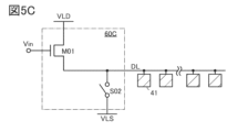
- 5A to 5C are circuit diagrams illustrating a semiconductor device.
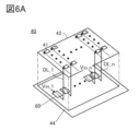
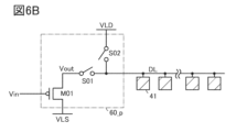
- 6A and 6B are circuit diagrams illustrating a semiconductor device.
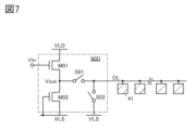
- FIG. 7 is a circuit diagram illustrating a semiconductor device.
- 8A to 8C are circuit diagrams illustrating a semiconductor device.
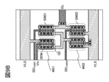
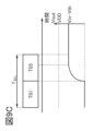
- 9A to 9C are circuit diagrams and layout diagrams illustrating a semiconductor device.
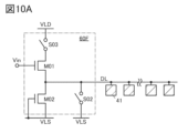
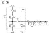
- 10A and 10B are circuit diagrams illustrating a semiconductor device.
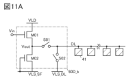
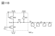
- 11A and 11B are circuit diagrams illustrating a semiconductor device.
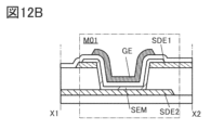
- FIG. 12A and 12B are a layout diagram and a cross-sectional view illustrating a semiconductor device.
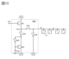
- FIG. 13 is a circuit diagram illustrating a semiconductor device.
- 14A and 14B are circuit diagrams illustrating a semiconductor device.
- 15A and 15B are circuit diagrams illustrating a semiconductor device.
- 16A and 16B are circuit diagrams illustrating a semiconductor device.
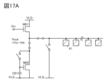
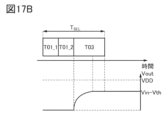
- 17A and 17B are circuit diagrams illustrating a semiconductor device.
- FIG. 18 is a layout diagram illustrating a semiconductor device.
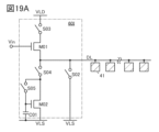
- 19A and 19B are circuit diagrams illustrating a semiconductor device.
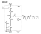
- 20A and 20B are circuit diagrams illustrating a semiconductor device.
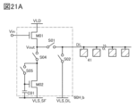
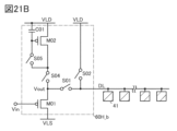
- 21A and 21B are circuit diagrams illustrating a semiconductor device.
- 22A and 22B are a layout diagram and a cross-sectional view illustrating a semiconductor device.
- FIG. 23 is a circuit diagram illustrating a semiconductor device.
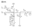
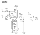
- 24A and 24B are circuit diagrams illustrating a semiconductor device.
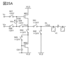
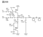
- 25A and 25B are circuit diagrams illustrating a semiconductor device.
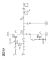
- 26A and 26B are circuit diagrams illustrating a semiconductor device.
- 27A and 27B are circuit diagrams illustrating a semiconductor device.
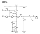
- 28A and 28B are circuit diagrams illustrating a semiconductor device.
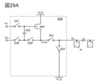
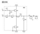
- 29A and 29B are circuit diagrams illustrating a semiconductor device.
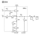
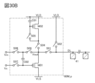
- 30A and 30B are circuit diagrams illustrating a semiconductor device.
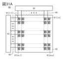
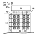
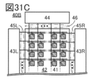
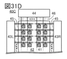
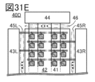
- 31A to 31E are block diagrams showing configuration examples of the display device.
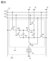
- FIG. 32 is a circuit diagram showing a configuration example of a semiconductor device.
- FIG. 33 is a timing chart showing an example of the operation of the semiconductor device.
- FIG. 32 is a circuit diagram showing a configuration example of a semiconductor device.
- FIG. 33 is a timing chart showing an example of the operation of the semiconductor device.
- FIG. 32 is a circuit diagram
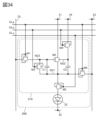
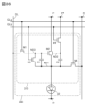
- FIG. 34 is a circuit diagram showing a configuration example of a semiconductor device.
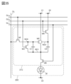
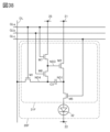
- FIG. 35 is a circuit diagram showing a configuration example of a semiconductor device.
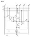
- FIG. 36 is a circuit diagram showing a configuration example of a semiconductor device.
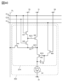
- FIG. 37 is a circuit diagram showing a configuration example of a semiconductor device.
- FIG. 38 is a circuit diagram showing a configuration example of a semiconductor device.
- FIG. 39 is a circuit diagram showing a configuration example of a semiconductor device.
- FIG. 40 is a circuit diagram showing a configuration example of a semiconductor device.
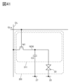
- FIG. 41 is a circuit diagram showing a configuration example of a semiconductor device.
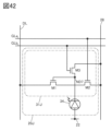
- FIG. 42 is a circuit diagram illustrating a semiconductor device.
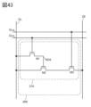
- FIG. 43 is a circuit diagram illustrating a semiconductor device.
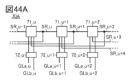
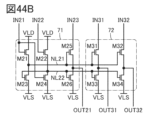
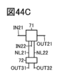
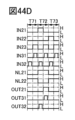
- 44A to 44C and 44E are circuit diagrams showing a configuration example of a semiconductor device, and Fig. 44D is a timing chart showing an operation example of the semiconductor device.
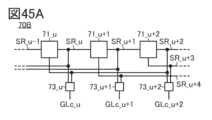
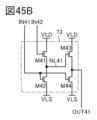
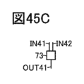
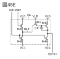
- 45A to 45C and 45E are circuit diagrams showing a configuration example of a semiconductor device, and Fig. 45D is a timing chart showing an operation example of the semiconductor device.
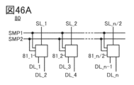
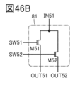
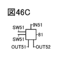
- 46A to 46C are circuit diagrams showing configuration examples of a semiconductor device.
- FIG. 47 is a circuit diagram showing a configuration example of a semiconductor device.
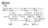
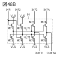
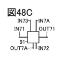
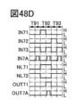
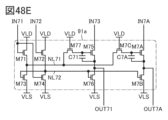
- 48A to 48C and 48E are circuit diagrams showing a configuration example of a semiconductor device, and Fig. 48D is a timing chart showing an operation example of the semiconductor device.
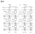
- FIG. 49 is a circuit diagram showing a configuration example of a semiconductor device.
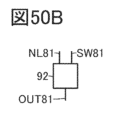
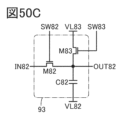
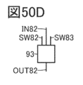
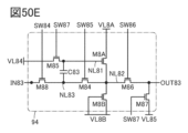
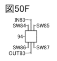
- FIG. 50A to 50F are circuit diagrams showing configuration examples of a semiconductor device.
- FIG. 51 is a timing chart showing an example of the operation of the semiconductor device.
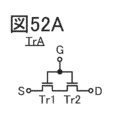
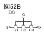
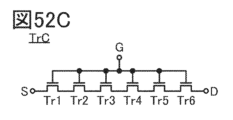
- 52A to 52C are circuit diagrams showing configuration examples of a semiconductor device.
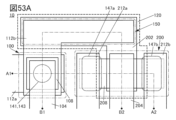
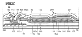
- Fig. 53A is a top view showing a configuration example of a semiconductor device, and Fig. 53B and Fig. 53C are cross-sectional views showing the configuration example of a semiconductor device.
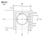
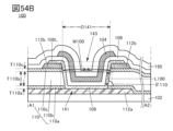
- 54A is a top view showing a configuration example of a semiconductor device, and FIG 54B is a cross-sectional view showing the configuration example of a semiconductor device.
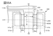
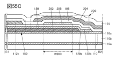
- Fig. 55A is a top view showing a configuration example of a semiconductor device, and Fig. 55B and Fig.
- FIG. 55C are cross-sectional views showing the configuration example of a semiconductor device.
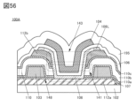
- FIG. 56 is a cross-sectional view showing a configuration example of a semiconductor device.
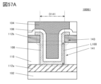
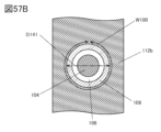
- 57A and 57B are cross-sectional views showing a configuration example of a semiconductor device.
- 58A and 58B are cross-sectional views showing a configuration example of a semiconductor device.
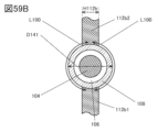
- 59A and 59B are cross-sectional views showing a configuration example of a semiconductor device.
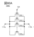
- 60A and 60B are circuit diagrams showing a configuration example of a semiconductor device
- Fig. 60C is a top view showing the configuration example of a semiconductor device.
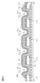
- FIG. 61 is a cross-sectional view showing a configuration example of a semiconductor device.
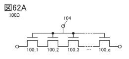
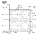
- FIG. 62A and 62B are circuit diagrams showing a configuration example of a semiconductor device, and Fig. 62C is a top view showing a configuration example of a semiconductor device.
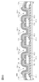
- FIG. 63 is a cross-sectional view showing a configuration example of a semiconductor device.
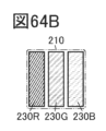
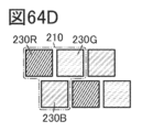
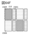
- Fig. 64A is a perspective view showing a configuration example of a display device, and Fig. 64B to Fig. 64F are top views showing an example of a pixel arrangement.
- 65A and 65B are cross-sectional views showing a configuration example of a display device.
- 66A and 66B are cross-sectional views showing a configuration example of a display device.
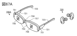
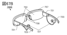
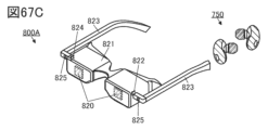
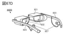
- 67A to 67D are diagrams showing an example of an electronic device.
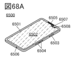
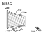
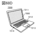
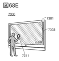
- 68A to 68F are diagrams showing an example of an electronic device.
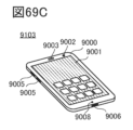
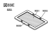
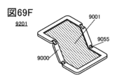
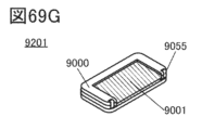
- 69A to 69G are diagrams showing an example of an electronic device.
- a semiconductor device is a device that utilizes semiconductor characteristics, such as a circuit including a semiconductor element (e.g., a transistor or a diode) or a device having such a circuit. It also refers to any device that can function by utilizing semiconductor characteristics.
- a semiconductor element e.g., a transistor or a diode
- an integrated circuit including a semiconductor element, a chip equipped with an integrated circuit, an electronic component in which a chip is housed in a package, or an electronic device equipped with an electronic component are examples of semiconductor devices.
- display devices for example, display devices, light-emitting devices, power storage devices, optical devices, imaging devices, lighting devices, arithmetic devices, control devices, memory devices, input devices, output devices, input/output devices, signal processing devices, electronic computers, or electronic devices may themselves be semiconductor devices and may have semiconductor devices.
- the size, layer thickness, or area may be exaggerated for clarity.
- the drawings are not limited to, for example, their size or aspect ratio.
- the drawings are schematic representations of ideal examples, and are not limited to, for example, the shapes or values shown in the drawings.
- layers or resist masks may be unintentionally thinned by processes such as etching, but this may not be reflected in the drawings to facilitate understanding.
- variations in voltage or current may occur due to noise or timing deviations, but this may not be reflected in the drawings to facilitate understanding.
- the components of the present invention may be classified by function and shown as independent elements.
- the elements shown in this specification and drawings, etc. are not limited to the explanations therein, and may be rephrased appropriately depending on the situation.
- an identifying symbol such as "A”, “b”, “_1”, “[n]”, or “[m, n]” may be added to the reference numeral.
- the identifying symbol may not be added.
- the "conductive state” or “on state” of a transistor refers to, for example, a state in which the source and drain of the transistor can be regarded as being electrically short-circuited, or a state in which a current can flow between the source and drain.
- a state in which the voltage between the gate and source of an n-channel transistor is higher than the threshold voltage, or a state in which the voltage between the gate and source of a p-channel transistor is lower than the threshold voltage may be referred to as the "conductive state” or "on state”.
- non-conductive state refers to a state in which the source and drain of the transistor can be regarded as being electrically cut off.
- a state in which the voltage between the gate and source of an n-channel transistor is lower than the threshold voltage, or a state in which the voltage between the gate and source of a p-channel transistor is higher than the threshold voltage may be referred to as the "non-conductive state", “cut-off state”, or "off state”.
- the voltage between the gate and source may be referred to as the "gate voltage”
- the voltage between the drain and source may be referred to as the “drain voltage”
- the voltage between the backgate and source may be referred to as the “backgate voltage”.
- the current flowing from the drain to the source may be referred to as the "drain current”.
- the "off current" of a transistor refers to the drain current when the transistor is in an off state. Note that in this specification, the off current and the current flowing from the gate to the source and drain (also referred to as gate leakage current) may be referred to as leakage current.
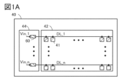
- FIG. 1A is a block diagram illustrating a configuration example of a display device including a semiconductor device.
- a display device 40 shown in FIG. 1A includes a display portion 42 and a driver circuit portion 44.
- the display portion 42 includes a plurality of pixels 41 electrically connected to wirings DL (wirings DL_1 to DL_n (n is an integer of 2 or more)).
- the driver circuit portion 44 includes a semiconductor device 60. Note that the wirings DL may be referred to as signal lines.
- a data potential is applied from the drive circuit unit 44 to the pixels 41 via the wiring DL, whereby light emission according to the data potential is controlled and an image is displayed on the display unit 42.
- the drive circuit unit 44, the display device 40, and the pixels 41 will be described later.
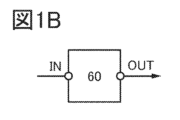
- the semiconductor device 60 is an analog circuit for outputting an output voltage according to an input voltage Vin (Vin_1 to Vin_n) to the wirings DL_1 to DL_n of each row (or each column). As shown in FIG. 1B, the semiconductor device 60 can be represented as a circuit block that outputs an input voltage applied to an input terminal IN from an output terminal OUT.
- FIG. 1C is a circuit diagram illustrating an example configuration of semiconductor device 60.
- Semiconductor device 60 has a transistor M01, a switch S01, and a switch S02.
- the gate of the transistor M01 is electrically connected to a wiring that provides an input voltage Vin to the input terminal IN.
- One of the source and drain of the transistor M01 is electrically connected to a wiring VLD.
- the other of the source and drain of the transistor M01 is electrically connected to a first terminal of the switch S01.
- the second terminal of the switch S01 is electrically connected to a first terminal of the switch S02 and a wiring DL.
- the second terminal of the switch S02 is electrically connected to a wiring VLS.
- the wiring VLD is a wiring that supplies a potential VDD (potential H) to an element such as a transistor.
- the wiring VLD is also called a first power supply line.
- the wiring VLS is a wiring that supplies a potential VSS (potential L) to an element such as a transistor.
- the wiring VLS is also called a second power supply line. The following description assumes that the potential VDD is a potential that is sufficiently higher than the potential VSS and is higher than the threshold voltage of the transistor in the semiconductor device 60.
- Transistor M01 has a function of providing an output voltage Vout corresponding to an input voltage Vin applied to its gate to wiring DL via switch S01.
- Transistor M01 functions as a source follower circuit in which the gate of transistor M01 is the input and the source of transistor M01 is the output. Note that in this specification, a transistor having a function similar to that of transistor M01 may be referred to as a "drive transistor.”
- the semiconductor device 60 having the transistor M01 can reduce the output impedance, thereby shortening the time it takes for the potential of the wiring DL to change in response to changes in the potential of the input voltage Vin, even when the load (parasitic capacitance) of the wiring DL is large. In other words, the semiconductor device 60 has an impedance conversion function.
- Switches S01 and S02 can be transistors, similar to transistor M01. By using transistors as switches S01 and S02, switches S01 and S02 can be manufactured through the same process as transistor M01. Note that switches other than switches S01 and S02 may also be transistors.
- the transistors (e.g., transistor M01) constituting the semiconductor device 60 are enhancement type (normally off type) n-channel transistors unless otherwise specified. Therefore, their threshold voltages are greater than 0 V.
- the semiconductor device 60 can be configured using various transistors.
- some or all of the transistors constituting the semiconductor device 60 may be p-channel transistors.
- transistors constituting the semiconductor device 60 transistors containing various semiconductors can be used.
- a transistor containing a single crystal semiconductor, a polycrystalline semiconductor, a microcrystalline semiconductor, or an amorphous semiconductor in a channel formation region can be used.
- the semiconductor is not limited to a single semiconductor whose main component is composed of a single element (such as silicon or germanium), but can be, for example, a compound semiconductor (such as silicon germanium or gallium arsenide), an oxide semiconductor, or the like.
- transistors that make up the semiconductor device 60 can be used as the transistors that make up the semiconductor device 60.
- MOS type field effect transistors can be used.
- transistors constituting the semiconductor device 60 transistors of various structures can be used.
- transistors of various structures such as planar type, staggered type, FIN type, TRI-GATE type, top gate type, bottom gate type, or dual gate type (structure in which gates are arranged on both sides (e.g., above and below) of a channel formation region) can be used.
- transistors constituting the semiconductor device 60 it is preferable to use vertical transistors (transistors in which at least a part of a semiconductor layer including a channel formation region is provided along the side of an insulating layer in an opening formed in the insulating layer).
- the source electrode and drain electrode are located at different heights, so current flows in the height direction (vertical direction) in the channel formation region of the semiconductor layer.
- the channel length direction has a height direction (vertical direction) component. Therefore, the above-mentioned vertical transistor can also be called a VFET (Vertical Field Effect Transistor), vertical channel transistor, vertical channel transistor, or vertical transistor.
- VFET Vertical Field Effect Transistor
- Vertical transistors have a structure in which the source region, the channel formation region, and the drain region can at least partially overlap when viewed from above, so that the area they occupy (also called the footprint) can be made small.
- the structure allows the channel length to be small and the channel width to be large, the on-resistance can be made small (the on-current can be made large).
- the source electrode and the drain electrode can be located at the same height, and current can flow in the circumferential (horizontal) direction in the channel formation region of the semiconductor layer.
- the channel width direction can have a height (vertical) component.
- a transistor with such a configuration can be called a VLFET (Vertical Lateral Field Effect Transistor). Since the VLFET has a structure that can reduce the occupied area while increasing the channel length, it can reduce short channel effects such as drain induced barrier lowering (DIBL).
- DIBL drain induced barrier lowering
- vertical transistors are preferably used as some or all of the transistors constituting the semiconductor device 60.
- vertical transistors are preferably used as transistors that function as switches (e.g., switches S01 and S02).
- a transistor with high saturation should be used as the drive transistor (e.g., transistor M01).
- the drive transistor e.g., transistor M01
- a transistor with a long channel length should be used.
- the above-mentioned VLFET may be used.
- an OS transistor (a transistor that includes an oxide semiconductor in a channel formation region) may be used as a transistor that constitutes the semiconductor device 60.
- the OS transistor has a characteristic of having an extremely low off-state current because the band gap of the oxide semiconductor in which the channel is formed is 2 eV or more.
- the off-state current value of the OS transistor per 1 ⁇ m of channel width at room temperature can be 1 aA (1 ⁇ 10 ⁇ 18 A) or less, 1 zA (1 ⁇ 10 ⁇ 21 A) or less, or 1 yA (1 ⁇ 10 ⁇ 24 A) or less.
- the off-state current value of a Si transistor (a transistor containing silicon in a channel formation region) per 1 ⁇ m of channel width at room temperature is 1 fA (1 ⁇ 10 ⁇ 15 A) or more and 1 pA (1 ⁇ 10 ⁇ 12 A) or less. Therefore, it can be said that the off-state current of an OS transistor is about 10 orders of magnitude lower than that of a Si transistor.
- the charge accumulated in a capacitor and a wiring having a parasitic capacitor can be held for a long period of time.
- the potential of the wiring DL can be held for a long period of time. Therefore, the power consumption of the semiconductor device can be reduced.
- the off-current of an OS transistor hardly increases even in a high-temperature environment. Specifically, the off-current hardly increases even in an environment of room temperature or higher and 200° C. or lower. Furthermore, the on-current of an OS transistor is unlikely to decrease even in a high-temperature environment.
- the on-current of a Si transistor decreases in a high-temperature environment. That is, the on-current of an OS transistor is higher than that of a Si transistor in a high-temperature environment.
- an OS transistor can perform a good switching operation even in an environment of 125° C. or higher and 150° C. or lower because the ratio of the on-current to the off-current is large. Therefore, a semiconductor device using an OS transistor can operate stably and with high reliability even in a high-temperature environment. That is, by using an OS transistor as a transistor constituting the semiconductor device 60, the reliability of the semiconductor device can be improved.
- OS transistors have a high withstand voltage between the source and drain (also referred to as drain withstand voltage). Therefore, a semiconductor device using an OS transistor can operate stably even when driven at a high voltage, and can achieve high reliability. That is, for example, by using an OS transistor as transistor M01 among the transistors constituting the semiconductor device 60, the operation of the semiconductor device 60 can be stabilized even when the potential difference (voltage) between the potential VDD and the potential VSS is large. Therefore, the reliability of the semiconductor device can be improved.
- one embodiment of the present invention is not limited to a configuration in which an OS transistor is used as the semiconductor device 60, and may be a configuration in which multiple types of transistors containing different semiconductor materials are used.
- the semiconductor device 60 may be configured with a transistor (LTPS transistor) containing low temperature polysilicon (LTPS) in the channel formation region, and an OS transistor.
- the LTPS transistor has high field-effect mobility and good frequency characteristics.
- a configuration in which an LTPS transistor and an OS transistor are combined may be referred to as LTPO.
- OS transistors can be used for the transistors functioning as switches S01 and S02
- an LTPS transistor can be used for the driving transistor (transistor M01).
- the transistors may be provided in different layers for each type of transistor.
- the semiconductor device 60 is configured with Si transistors and OS transistors
- a layer containing the Si transistors and a layer containing the OS transistors may be stacked. With such a configuration, the area occupied by the semiconductor device 60 can be reduced.
- vertical OS transistors may be used as the transistors functioning as switches S01 and S02, and a dual-gate OS transistor may be used as the driver transistor (transistor M01).
- a driver transistor transistor M01
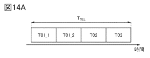
- the semiconductor device 60 performs an initialization operation T01, an initialization ending operation T02, and a signal output operation T03 during a period TSEL during which the semiconductor device 60 outputs an output voltage corresponding to the input voltage Vin.
- the semiconductor device 60 may omit the initialization ending operation T02 as shown in Fig. 2B.
- the time required for the initialization operation T01 and the signal output operation T03 can be set long, and therefore a stable output voltage can be obtained.
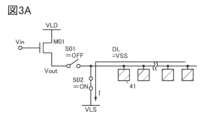
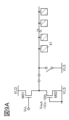
- FIG. 3A is a circuit diagram for explaining the initialization operation T01.
- the initialization operation T01 the potential of the wiring DL is initialized.
- the initialization operation T01 is performed with the switch S01 in a non-conducting state (OFF) and the switch S02 in a conducting state (ON).
- the switch S02 has a function of performing the initialization operation to initialize the potential of the wiring DL by being in a conducting state.
- the switch S01 is in a non-conducting state, so the output voltage Vout (the voltage on the first terminal side of the switch S01) corresponding to the input voltage Vin does not change.
- the switch S02 is turned on, so that the potential of the wiring DL can be set to the potential VSS.
- the initialization operation T01 will be described as an operation for discharging the charge of the wiring DL. Note that the initialization operation is sometimes called a discharging operation.
- the potential of the wiring DL changes depending on the current I that flows through the switch S02.
- a transistor can be used for the switch S02, similar to the transistor M01. The same applies to the switch S01.
- switch S02 is a transistor
- a bias voltage may be applied to the gate of the transistor so that a bias current flows.
- the transistor may be operated by switching between allowing or not allowing a bias current to flow, depending on whether or not a bias voltage is applied.
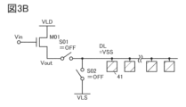
- FIG. 3B is a circuit diagram for explaining the initialization end operation T02.
- both switches S01 and S02 are in a non-conducting state (OFF).
- the potential VSS of the wiring DL set in the initialization operation T01 is maintained.
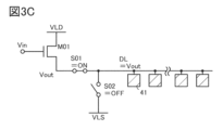
- FIG. 3C is a circuit diagram for explaining the signal output operation T03.
- a current flows through the transistor M01 by turning the switch S01 on (ON).
- the wiring DL becomes the output voltage Vout.
- the switch S01 When the switch S01 is turned on, it has the function of performing a signal output operation that provides the output voltage Vout to the wiring DL.
- Vout When the output voltage Vout becomes Vin-Vth, a voltage equal to or lower than Vth, which corresponds to the threshold voltage of transistor M01, is applied between the gate and source of transistor M01, causing a subthreshold current to flow between the source and drain.
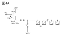
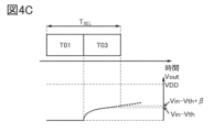
- the period TSEL during which the output voltage according to the input voltage Vin is output may end before the output voltage Vout increases to Vin-Vth (see FIG. 4B). In this case, the output voltage Vout becomes Vin-Vth- ⁇ ( ⁇ >0), which is smaller than Vin-Vth.
- the output voltage Vout can rise to Vin-Vth. Since a voltage equal to or lower than Vth, which corresponds to the threshold voltage of the transistor M01, is applied between the gate and source of the transistor M01, a subthreshold current flows between the source and drain. Since a subthreshold current flows through the transistor M01, the output voltage Vout may continue to rise until the end of the period TSEL (see FIG. 4C). In this case, the output voltage Vout becomes Vin-Vth+ ⁇ ( ⁇ >0), which is larger than Vin-Vth.
- One aspect of the present invention reduces power consumption by blocking or reducing the bias current flowing through a source follower circuit. Specifically, the number of transistors to which a bias voltage is applied is reduced, and the steady flow of bias current is suppressed, thereby reducing power consumption. If the bias current does not flow steadily, it may take some time (also called the settling time) until the output voltage according to the input voltage stabilizes. In particular, the settling time may be long when changing the voltage of the signal line in a decreasing direction.
- the conductive state of the switch is changed over to perform an initialization operation and then a signal output operation.
- charging to a desired voltage by the signal output operation can be performed in a state where the voltage of the signal line is lowered before the signal output operation is performed. Therefore, when inputting an input voltage, even if the voltage of the signal line is changed in a lowering direction, it can be changed to a desired voltage.
- a vertical transistor in order to reduce the settling time, it is preferable to use a vertical transistor as the driving transistor.
- the footprint of the driving transistor can be reduced, and the channel length and channel width can be increased.
- a vertical driving transistor can reduce the on-resistance (increase the on-current), but consumes more power. Therefore, by combining it with the above-described configuration in which a signal output operation is performed after the initialization operation, it is possible to improve the operating speed of a display device having a semiconductor device while suppressing increases in the area occupied by the semiconductor device and power consumption.
- one aspect of the present invention is not limited to the configuration example of the semiconductor device 60 described above.
- Figs. 5A to 5C modified examples of the semiconductor device 60 described above are described.
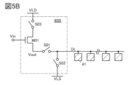
- the switch S01 may be located in the path between the wiring VLD and the wiring DL.
- a switch having the function of the switch S01 may be provided between the drain side of the transistor M01 and the wiring VLD.
- the switch S01 in the semiconductor device 60 shown in FIG. 1C may be omitted in cases where the period required for the initialization operation is short.
- the semiconductor device 60A shown in FIG. 5A is a modified example of the semiconductor device 60 shown in FIG. 1C in which the switch S01 in the semiconductor device 60 shown in FIG. 1C is omitted and a new switch S03 is added.
- the semiconductor device 60B shown in FIG. 5B is a modified example of the semiconductor device 60 shown in FIG. 1C in which a switch S03 is added to the semiconductor device 60 shown in FIG. 1C.
- the semiconductor device 60C shown in FIG. 5C is a modified example of the semiconductor device 60 shown in FIG. 1C in which the switch S01 in the semiconductor device 60 shown in FIG. 1C is omitted.
- the arrangement of switch S01 and the number of switches having the function of switch S01 can be changed as appropriate.
- the arrangement of switch S01 it is possible to increase the degree of freedom in design.
- by increasing the number of switches it is possible to further reduce the current flowing through transistor M01 during the initialization operation.
- the display section 42 and the drive circuit section 44 may be arranged so as to overlap each other.
- the display section 42 having the pixels 41 may be provided on a layer above the layer on which the drive circuit section 44 having the semiconductor device 60 is provided.
- the transistors in the display unit 42 and the transistors in the drive circuit unit 44 can be arranged in different layers. Therefore, transistors with different structures can be applied to the transistors in the display unit 42 or the transistors in the drive circuit unit 44.
- connection distance (wiring length) between the pixels 41 of the display section 42 and the semiconductor device 60 of the drive circuit section 44 can be made extremely short.
- the wiring resistance and parasitic capacitance of the wiring DL are reduced, so the time required for charging and discharging is shortened, and high-speed driving can be achieved. Also, power consumption can be reduced. Also, miniaturization and weight reduction can be achieved.
- FIG. 6B shows a configuration example of a semiconductor device 60_p in which a p-channel transistor is used for the transistor M01.
- the potential of each wiring may be set so that the high and low potentials are inverted.
- the wiring DL that is discharged via the switch S02 in FIG. 1C may be configured to be charged by the wiring VLD in FIG. 6B.
- FIG. 7 is a circuit diagram illustrating an example of the configuration of semiconductor device 60D.
- Semiconductor device 60D has transistor M02 in addition to transistor M01, switch S01, and switch S02. Note that the explanations of transistor M01, switch S01, and switch S02 in semiconductor device 60D overlap with the explanation of semiconductor device 60 described above, and therefore may be omitted.
- the gate of the transistor M02 is electrically connected to the wiring VLS.
- One of the source and drain of the transistor M02 is electrically connected to the other of the source and drain of the transistor M01 and the first terminal of the switch S01.
- the other of the source and drain of the transistor M02 is electrically connected to the wiring VLS.
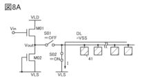
- transistor M02 Because the gate and source voltages of transistor M02 are equipotential, that is, 0 V is applied as the gate-source voltage Vgs, a subthreshold current flows between the source and drain. Transistor M02 functions as a current source that passes subthreshold current. The subthreshold current that flows through transistor M02 is much smaller than the current that flows through transistor M01 when charging line DL.
- a transistor that functions like transistor M02 may be called a "load transistor.” Note that transistor M02 that functions as a load transistor may be replaced with, for example, a resistive element.
- the description of the drive transistor can be referred to as an example of the configuration of the load transistor (transistor M02).
- a transistor with high saturation and a large channel length may be used as the load transistor.
- the semiconductor device 60D performs an initialization operation T01, an initialization ending operation T02, and a signal output operation T03 during a period TSEL during which an output voltage corresponding to an input voltage Vin is output, similar to the semiconductor device 60 described above. Note that the semiconductor device 60D may omit the initialization ending operation T02 as illustrated in FIG. 2B.
- FIG. 8A is a circuit diagram for explaining the initialization operation T01 in a schematic manner.
- the explanation of the initialization operation T01 in FIG. 8A is the same as that in FIG. 3A.
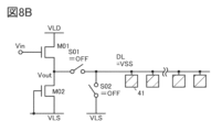
- FIG. 8B is a circuit diagram for illustrating the initialization end operation T02.
- the explanation of the initialization end operation T02 in FIG. 8B is the same as that in FIG. 3B.
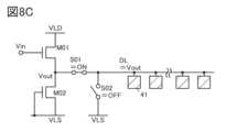
- FIG. 8C is a circuit diagram for illustrating signal output operation T03.
- the explanation of signal output operation T03 in FIG. 8C is the same as that in FIG. 3C.
- Vout When the output voltage Vout becomes Vin-Vth, a voltage equal to or lower than Vth, which corresponds to the threshold voltage of transistor M01, is applied between the gate and source of transistor M01, causing a subthreshold current to flow between the source and drain.
- Semiconductor device 60D has a configuration including transistor M02. Therefore, during signal output operation T03, a subthreshold current also flows through transistor M02.
- the subthreshold current flowing through transistor M02 is preferably designed to be the same in magnitude as the subthreshold current flowing through transistor M01. For example, as shown in the layout diagram of FIG. 9B, it is preferable that the areas of the overlapping regions between the semiconductor layer SEM and the wiring GE functioning as the gate electrode in transistors M01 and M02 are approximately the same. With this configuration, the subthreshold current flowing through transistor M02 can be made close to the same in magnitude as the subthreshold current flowing through transistor M01.
- signals SEL SW01 and SEL SW02 are shown as signals for controlling the conductive states of switches S01 and S02.
- the signals SEL SW01 and SEL SW02 are signals provided to the gates of transistors functioning as switches.
- one aspect of the present invention is not limited to the configuration example of the semiconductor device 60D described above.
- Figs. 10A and 12B a modified example of the semiconductor device 60D described above is described.
- the switch S01 may be located in the path between the wiring VLD and the wiring DL.
- a switch having the function of the switch S01 may be provided between the drain side of the transistor M01 and the wiring VLD.
- the switch S01 in the semiconductor device 60D shown in FIG. 7 can be omitted in cases where the period required for the initialization operation is short.
- the semiconductor device 60F shown in FIG. 10A is a modified example of the semiconductor device 60D shown in FIG. 7, in which the switch S01 in the semiconductor device 60D shown in FIG. 7 is omitted and a new switch S03 is provided.
- the semiconductor device 60G shown in FIG. 10B is a modified example of the semiconductor device 60D shown in FIG. 7, in which the switch S03 is added to the semiconductor device 60D shown in FIG. 7.
- the arrangement of switch S01 and the number of switches having the function of switch S01 can be changed as appropriate. Being able to change the arrangement of switch S01 as appropriate increases the degree of freedom in design. Also, by increasing the number of switches, the current flowing through transistor M01 during the initialization operation can be made smaller.
- the wiring VLS electrically connected to the other of the source and drain of the transistor M02 and the wiring VLS electrically connected to the second terminal of the switch S02 may be different wirings.
- FIG. 11A shows a configuration example of a semiconductor device 60D_b in which the wiring electrically connected to the other of the source and drain of the transistor M02 is wiring VLS_SF and the wiring electrically connected to the second terminal of the switch S02 is wiring VLS_DL.
- the potentials of the wirings VLS_SF and VLS_D may be the same potential VSS or different potentials.
- FIG. 11B shows a configuration example of a semiconductor device 60D_p in which p-channel transistors are used for the transistors M01 and M02.
- the potential of each wiring may be set so that the high and low potentials are inverted.
- the wiring DL that is discharged via the switch S02 in FIG. 7 may be configured to be charged by the wiring VLD in FIG. 11B.
- FIG. 12A shows a modified version of the layout diagram shown in FIG. 9B.
- VFETs are used for the transistors M01 and M02 and the transistors that function as switches S01 and S02.
- a VFET can have at least a portion of the source region, the channel formation region, and the drain region overlap.
- FIG. 12B shows a cross-sectional view between the dashed lines X1-X2 in FIG. 12A.
- a VFET has a configuration in which the electrodes SDE1 and SDE2 that contact the source region or drain region, the semiconductor layer SEM having the channel formation region, and the wiring GE that becomes the gate electrode overlap.
- This allows the occupied area (also called the footprint) to be small.
- the on-resistance can be small (the on-current can be large).
- a VLFET can be applied to FIG. 12A as a modified version of the above-mentioned vertical transistor.
- FIG. 13 is a circuit diagram illustrating an example configuration of semiconductor device 60H.
- semiconductor device 60H has switches S04, S05, and a capacitor C01. Note that the explanations of transistors M01, M02, switches S01, and S02 in semiconductor device 60H may be omitted because they overlap with the explanations of semiconductor devices 60 and 60D described above.
- the first terminal of the switch S04 is electrically connected to the other of the source and drain of the transistor M01 and the first terminal of the switch S01.
- the second terminal of the switch S04 is electrically connected to one of the source and drain of the transistor M02 and the first terminal of the switch S05.
- the second terminal of the switch S05 is electrically connected to the gate of the transistor M02 and the first electrode of the capacitor C01.
- the wiring VLS is electrically connected to the other of the source and drain of the transistor M02 and the second electrode of the capacitor C01.
- Switches S04 and S05 have the function of controlling the charging or discharging of capacitor C01 by controlling the conductive state.
- Capacitor C01 has the function of holding the gate-source voltage of transistor M02. The charge stored in capacitor C01 can be discharged through the source and drain of transistor M02 to hold the threshold voltage of transistor M02.
- the threshold voltage of transistor M02 is applied as a bias voltage to transistor M02, and transistor M02 has the function of passing a bias current corresponding to the threshold voltage.
- Transistor M02 has the function of a current source that passes a bias current corresponding to the threshold voltage. The bias current flowing through transistor M02 according to the threshold voltage is much smaller than the current flowing through transistor M01 when charging line DL.
- the threshold voltage of transistor M02 is described as being Vth, the same as the threshold voltage of transistor M01, but it may be a different value.
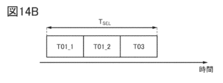
- the semiconductor device 60H performs a first initialization operation T01_1, a second initialization operation T01_2, an initialization ending operation T02, and a signal output operation T03 during a period TSEL during which the semiconductor device 60H outputs an output voltage corresponding to the input voltage Vin.
- the semiconductor device 60H may omit the initialization ending operation T02 as shown in Fig. 14B.
- the times required for the first initialization operation T01_1, the second initialization operation T01_2, and the signal output operation T03 can be set long, and therefore a stable output voltage can be obtained.
- FIG. 15A is a circuit diagram for illustrating a schematic of the first initialization operation T01_1.
- the potential of the wiring DL is initialized and the capacitor C01 is charged.
- the first initialization operation T01_1 is performed with the switch S01 in a non-conductive state (OFF) and the switches S02, S04, and S05 in a conductive state (ON).
- the switches S04 and S05 have the function of charging the capacitor C01 by being in a conductive state.
- the switches S04 and S05 are in a conductive state, so a current I1 flows according to the input voltage Vin.
- a voltage for passing the current I1 is held in the capacitor C01 as the gate-source voltage of the transistor M02.
- the input voltage Vin is set to a voltage at which the current I1 flows through the transistors M01 and M02 during the first initialization operation T01_1.
- the switch S02 is in a conductive state, so the potential of the line DL changes to the potential VSS due to the current I2 flowing through the switch S02.
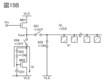
- FIG. 15B is a circuit diagram for illustrating the second initialization operation T01_2.
- the capacitor C01 is discharged.
- the second initialization operation T01_2 is performed with the switches S01 and S04 in a non-conductive state (OFF) and the switches S02 and S05 in a conductive state (ON).
- the switches S04 and S05 have the function of discharging the capacitor C01 by putting the switch S04 in a non-conductive state and the switch S05 in a conductive state.
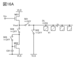
- FIG. 16A is a circuit diagram for explaining the initialization end operation T02.
- the switches S01, S02, S04, and S05 are all in a non-conducting state (OFF).
- the potential VSS of the wiring DL set in the initialization operation T01_2 and the threshold voltage of the transistor M02 are held in the capacitor C01.
- FIG. 16B is a circuit diagram for explaining the signal output operation T03.
- a current flows through the transistor M01 by turning the switch S01 on (ON).
- the wiring DL becomes the output voltage Vout.
- the switch S01 When the switch S01 is turned on, it has the function of performing a signal output operation that provides the output voltage Vout to the wiring DL.
- a current flows through transistor M02 by turning switch S04 conductive (ON).
- the current flowing through transistor M02 is a current at the threshold voltage of transistor M02.
- a subthreshold current flows between the gate and source of transistor M02.
- Switches S04 and S05 have the function of passing a subthreshold current through transistor M02 by turning switch S04 conductive and switch S05 non-conductive.
- the subthreshold current flowing through transistor M02 is a current that corresponds to the threshold voltage held between the gate and source of transistor M02. Therefore, even if the transistor characteristics fluctuate in response to fluctuations in the threshold voltage, a small, constant current can flow.
- Vout When the output voltage Vout becomes Vin-Vth, a voltage equal to or lower than Vth, which corresponds to the threshold voltage of transistor M01, is applied between the gate and source of transistor M01, causing a subthreshold current to flow between the source and drain.
- Semiconductor device 60H has a configuration including transistor M02. Therefore, during signal output operation T03, a subthreshold current also flows through transistor M02.
- the subthreshold current flowing through transistor M02 is preferably designed to be the same in magnitude as the subthreshold current flowing through transistor M01. For example, as shown in the layout diagram of FIG. 18, it is preferable that the areas of the overlapping regions between the semiconductor layer SEM and the wiring GE functioning as the gate electrode in transistors M01 and M02 are approximately the same. With this configuration, the subthreshold current flowing through transistor M02 can be made close to the same in magnitude as the subthreshold current flowing through transistor M01.
- signals SEL SW04 and SEL SW05 are shown as signals for controlling the conductive states of switches S04 and S05.
- the signals SEL SW04 and SEL SW05 are signals given to the gates of transistors functioning as switches.
- One aspect of the present invention reduces power consumption by blocking or reducing the bias current flowing through a source follower circuit.
- a transistor to which a bias voltage is applied is designed to have a gate and source connected so that a subthreshold current flows, and power consumption can be reduced by preventing the bias current from flowing steadily. If the bias current does not flow steadily, it may take some time (also called the settling time) for the output voltage according to the input voltage to stabilize. In particular, the settling time may be long when changing the voltage of the signal line in a downward direction.
- the conductive state of the switch is changed over to perform an initialization operation and then a signal output operation.
- charging to a desired voltage by the signal output operation can be performed in a state where the voltage of the signal line is lowered before the signal output operation is performed. Therefore, when inputting an input voltage, even if the voltage of the signal line is changed in a lowering direction, it can be changed to a desired voltage.
- a vertical transistor in order to reduce the settling time, it is preferable to use a vertical transistor as the driving transistor.
- the footprint of the driving transistor can be reduced, and the channel length and channel width can be increased.
- a vertical driving transistor can reduce the on-resistance (increase the on-current), but consumes more power. Therefore, by combining it with the above-described configuration in which a signal output operation is performed after the initialization operation, it is possible to improve the operating speed of a display device having a semiconductor device while suppressing increases in the area occupied by the semiconductor device and power consumption.
- one embodiment of the present invention is not limited to the configuration example of the semiconductor device 60H described above. Modifications of the semiconductor device 60H described above are described in Figures 19A to 22B.
- the switch S01 may be located in the path between the wiring VLD and the wiring DL.
- a switch having the function of the switch S01 may be provided between the drain side of the transistor M01 and the wiring VLD.
- the switch S01 in the semiconductor device 60H shown in FIG. 13 may be omitted in cases where the period required for the initialization operation is short.
- Semiconductor device 60I shown in FIG. 19A is a modified example of semiconductor device 60H shown in FIG. 13, in which switch S01 in semiconductor device 60H shown in FIG. 13 is omitted and a new switch S03 is provided.
- Semiconductor device 60J shown in FIG. 19B is a modified example of semiconductor device 60H shown in FIG. 13, in which switch S03 is added to semiconductor device 60H shown in FIG. 13.
- the switch S04 may be located in the path between the wiring VLD and the transistor M02.
- a switch having the function of the switch S04 may be provided between the source side of the transistor M01 and the switch S01.
- the semiconductor device 60K shown in FIG. 20A is a modified example of the semiconductor device 60H shown in FIG. 13, in which the switch S04 in the semiconductor device 60H shown in FIG. 13 is omitted and a new switch S06 is provided.
- the semiconductor device 60L shown in FIG. 20B is a modified example of the semiconductor device 60H shown in FIG. 13, in which a switch S06 is added to the semiconductor device 60H shown in FIG. 13.
- the arrangement of switch S01 or switch S04 and the number of switches having the functions of switch S01 or switch S04 can be changed as appropriate.
- the arrangement of switch S01 or switch S04 it is possible to increase the degree of freedom in design. Also, by increasing the number of switches, it is possible to further reduce the current flowing through transistor M01 or switch S04 during the initialization operation.
- the wiring VLS electrically connected to the other of the source and drain of the transistor M02 and the wiring VLS electrically connected to the second terminal of the switch S02 may be different wirings.
- FIG. 21A shows a configuration example of a semiconductor device 60H_b in which the wiring electrically connected to the other of the source and drain of the transistor M02 is wiring VLS_SF and the wiring electrically connected to the second terminal of the switch S02 is wiring VLS_DL.
- the potentials of the wirings VLS_SF and VLS_D may be the same potential VSS or different potentials.
- FIG. 21B shows a configuration example of a semiconductor device 60H_p in which p-channel transistors are used for the transistors M01 and M02.
- the potential of each wiring may be set so that the high and low potentials are inverted.
- the wiring DL that is discharged via the switch S02 in FIG. 13 may be configured to be charged by the wiring VLD in FIG. 21B.
- FIG. 22A shows a modified version of the layout diagram shown in FIG. 18.
- VFETs are used as the transistors M01 and M02 and the transistors that function as the switches S01, S02, S04, and S05.
- a VFET can have at least a portion of the source region, the channel formation region, and the drain region overlap.
- FIG. 22B shows a cross-sectional view between the dashed lines X1-X2 in FIG. 22A.
- a VFET has a configuration in which the electrodes SDE1 and SDE2 in contact with the region that will become the source region or the drain region, the semiconductor layer SEM having the channel formation region, and the wiring GE that will become the gate electrode overlap. This allows the occupied area (also called the footprint) to be reduced.
- a VLFET can also be applied to FIG. 22A as a modified version of the above-mentioned vertical transistor.
- FIG. 23 is a circuit diagram illustrating an example of the configuration of semiconductor device 60M.
- semiconductor device 60M also has switches S07 to S09 and capacitor C02. Note that the explanations of transistor M01, transistor M02, switch S01, switch S02, switch S04, switch S05, and capacitor C01 in semiconductor device 60M may be omitted because they overlap with the explanations of semiconductor devices 60, 60D, and 60H described above.
- the first terminal of the switch S07 is electrically connected to a terminal that provides a potential Vx.
- the second terminal of the switch S07 is electrically connected to a first electrode of the capacitor C02 and the gate of the transistor M01.
- the first terminal of the switch S08 is electrically connected to a terminal that provides an input voltage Vin.
- the second terminal of the switch S08 is electrically connected to a second electrode of the capacitor C02 and a first terminal of the switch S09.
- the second terminal of the switch S09 is electrically connected to a first terminal of the switch S04, the other of the source and drain of the transistor M01, and the first terminal of the switch S01.
- the potential Vx is a voltage for making the transistor M01 conductive during the first initialization operation.
- the potential Vx may be the potential VDD.
- the switch S07 has a function of controlling whether or not the potential Vx is applied to the gate of the transistor M01 by controlling the conductive state.
- the switch S08 has a function of controlling whether or not the input voltage Vin is applied to the second electrode of the capacitor C02 by controlling the conductive state.
- the switch S09 has a function of controlling the conductive state to control the retention of the threshold voltage of the transistor M01 in the capacitor C02 by charging and discharging the capacitor C02.
- Capacitor C02 has the function of holding a voltage for turning on transistor M01 during the first initialization operation.
- Capacitor C02 which has been charged with a voltage for turning on transistor M01 during the first initialization operation, holds the threshold voltage of transistor M02 by the current flowing through the source and drain of transistor M01 during the second initialization operation.
- the threshold voltage of transistor M01 held in capacitor C02 is held during the second initialization operation, the initialization end operation, and the signal output operation.
- Vth threshold voltage
- the semiconductor device 60M performs a first initialization operation T01_1, a second initialization operation T01_2, an initialization ending operation T02, and a signal output operation T03 during a period TSEL during which an output voltage corresponding to an input voltage Vin is output. Note that the semiconductor device 60M may omit the initialization ending operation T02 as illustrated in FIG. 14B.
- FIG. 24A is a circuit diagram for explaining the first initialization operation T01_1.
- the potential of the wiring DL is initialized and the capacitor C01 is charged.
- the first initialization operation T01_1 is performed with the switches S01, S08, and S09 in a non-conductive state (OFF) and the switches S02, S04, S05, and S07 in a conductive state (ON).
- the switch S07 By making the switch S07 conductive, the potential Vx is held in the capacitor C02 and a current I1 flows through the transistor M01.
- the potential Vx is set to a voltage at which the current I1 flows through the transistors M01 and M02 during the first initialization operation T01_1.
- the switches S04 and S05 are in a conductive state, so a current I1 corresponding to the potential Vx flows.
- a voltage for passing the current I1 is held in the capacitor C01 as the gate-source voltage of the transistor M02.
- the switch S02 is in a conductive state, so the potential of the line DL changes to the potential VSS due to the current I2 flowing through the switch S02.
- FIG. 24B is a circuit diagram for illustrating the second initialization operation T01_2.
- the second initialization operation T01_2 is performed with switches S01, S04, and S08 in a non-conductive state (OFF), and switches S02, S05, S07, and S09 in a conductive state (ON).
- Switches S04 and S05 have the function of discharging capacitor C01 by setting switch S04 in a non-conductive state and switch S05 in a conductive state.
- Switches S07, S08, and S09 have the function of discharging capacitor C02 by setting switch S08 in a non-conductive state and switches S07 and S09 in a conductive state.
- capacitor C2 When capacitor C2 is discharged, a current I4 flows, and the current I4 becomes small when the gate-source voltage of transistor M01 becomes the threshold voltage of transistor M01. In other words, when capacitor C02 is discharged, the threshold voltage of transistor M01 is held in capacitor C02.
- FIG. 25A is a circuit diagram for illustrating the initialization end operation T02.
- switches S01, S02, S04, S05, S07, S08, and S09 are all in a non-conducting state (OFF).
- the potential VSS of the wiring DL set in the initialization operation T01_2 is held, and the threshold voltage of the transistor M02 is held in the capacitor C01.
- the threshold voltage of the transistor M01 is held in the capacitor C02.
- FIG. 25B is a circuit diagram for explaining the signal output operation T03.
- a current flows through the transistor M01 by turning the switch S01 on (ON).
- the wiring DL becomes the output voltage Vout.
- the switch S01 When the switch S01 is turned on, it has the function of performing a signal output operation that provides the output voltage Vout to the wiring DL.
- switch S07 is turned off (OFF) to put the first electrode side of capacitor C02, i.e., the gate of transistor M01, into an electrically floating state (floating), and switch S08 is turned on (ON). Therefore, with a voltage corresponding to the threshold voltage (Vth) of transistor M01 held across capacitor C02, the potential of the second electrode side of capacitor C02 becomes the input voltage Vin. Therefore, due to the capacitive coupling of capacitor C02, the potential of the first electrode side of capacitor C02, i.e., the gate of transistor M01, becomes Vin+Vth.
- Vth threshold voltage
- the potential of the gate of transistor M01 is set to Vin+Vth, and the switch S01 is turned on (ON), so that the current flowing through transistor M01 is reduced by the gate-source voltage of transistor M01 being equal to or lower than Vth.
- the output voltage Vout can be a voltage with the threshold voltage Vth corrected.
- a current flows through transistor M02 by turning switch S04 conductive (ON).
- the current flowing through transistor M02 is a current at the threshold voltage of transistor M02.
- a subthreshold current flows between the gate and source of transistor M02.
- Switches S04 and S05 have the function of passing a subthreshold current through transistor M02 by turning switch S04 conductive and switch S05 non-conductive.
- the subthreshold current flowing through transistor M02 is a current that corresponds to the threshold voltage held between the gate and source of transistor M02. Therefore, even if the transistor characteristics fluctuate in response to fluctuations in the threshold voltage, a small, constant current can flow.
- Vout When the output voltage Vout becomes Vin, a voltage equal to or lower than Vth, which corresponds to the threshold voltage of transistor M01, is applied between the gate and source of transistor M01, causing a subthreshold current to flow between the source and drain.
- Semiconductor device 60M has a configuration including transistor M02. Therefore, during signal output operation T03, a subthreshold current also flows through transistor M02.
- the subthreshold current flowing through the transistor M02 is the same as the subthreshold current flowing through the transistor M01.
- the area of the region where the semiconductor layer SEM and the wiring GE functioning as the gate electrode overlap in the transistor M01 and the transistor M02 is preferable to make the area of the region where the semiconductor layer SEM and the wiring GE functioning as the gate electrode overlap in the transistor M01 and the transistor M02 approximately the same.
- the subthreshold current (I st ) flowing through the transistor M02 shown in FIG. 26A can be made to approach the same magnitude as the subthreshold current (I st ) flowing through the transistor M01.
- one aspect of the present invention is not limited to the configuration example of the semiconductor device 60M described above. Modifications of the semiconductor device 60M described above are described in Figures 27A to 30B.
- the switch S01 may be located in the path between the wiring VLD and the wiring DL.
- a switch having the function of the switch S01 may be provided between the drain side of the transistor M01 and the wiring VLD.
- the switch S01 in the semiconductor device 60M shown in FIG. 23 may be omitted in cases where the period required for the initialization operation is short.
- the potential Vx may be the potential VDD.
- the semiconductor device 60N shown in FIG. 27A is a modified example of the semiconductor device 60M shown in FIG. 23, in which the switch S01 in the semiconductor device 60M shown in FIG. 23 is omitted and a new switch S03 is provided.
- the semiconductor device 60O shown in FIG. 27B is a modified example of the semiconductor device 60M shown in FIG. 23, in which the terminal for applying the potential Vx in the semiconductor device 60M shown in FIG. 23 is connected to the wiring VLD.
- the switch S04 may be located in the path between the wiring VLD and the transistor M02.
- a switch having the function of the switch S04 may be provided between the drain side of the transistor M01 and the switch S01.
- the semiconductor device 60P shown in FIG. 28A is a modified example of the semiconductor device 60M shown in FIG. 23, in which the switch S04 in the semiconductor device 60M shown in FIG. 23 is omitted and a new switch S06 is provided.
- the semiconductor device 60Q shown in FIG. 28B is a modified example of the semiconductor device 60M shown in FIG. 23, in which the switches S03 and S06 are added to the semiconductor device 60M shown in FIG. 23.
- the switches S04, S05, and the transistor M02 can be omitted, as in FIG. 1C described above. Also, in the configuration example of the semiconductor device 60M shown in FIG. 23, the switches S04, S05, and the transistor M02 can be replaced with the configuration of the transistor M02 described in FIG. 7 described above.
- the semiconductor device 60R shown in FIG. 29A is a modified example of the semiconductor device 60M shown in FIG. 23 in which the switches S04, S05, and transistor M02 in the semiconductor device 60M shown in FIG. 23 are omitted.
- the semiconductor device 60S shown in FIG. 29B is a modified example of the semiconductor device 60M shown in FIG. 23 in which the switches S04, S05, and transistor M02 in the semiconductor device 60M shown in FIG. 23 are replaced with the configuration of the transistor M02 described in FIG. 7 above.
- the wiring VLS electrically connected to the other of the source and drain of the transistor M02 and the wiring VLS electrically connected to the second terminal of the switch S02 may be different wirings.
- FIG. 30A shows a configuration example of a semiconductor device 60M_b in which the wiring electrically connected to the other of the source and drain of the transistor M02 is wiring VLS_SF and the wiring electrically connected to the second terminal of the switch S02 is wiring VLS_DL.
- the potentials of the wirings VLS_SF and VLS_D may be the same potential VSS or different potentials.
- FIG. 30B shows a configuration example of a semiconductor device 60M_p in which p-channel transistors are used for the transistors M01 and M02.
- the potential of each wiring may be set so that the high and low potentials are inverted.
- the wiring DL that is discharged via the switch S02 in FIG. 23 may be configured to be charged by the wiring VLD in FIG. 30B.
- the arrangement of the switches and the number of switches can be changed as appropriate.
- the arrangement of the switches it is possible to increase the degree of freedom in design.
- the number of switches it is possible to further reduce the current flowing through transistor M01 during the initialization operation.
- 31A to 31E are block diagrams illustrating configuration examples of a display device according to one embodiment of the present invention.
- the display device 40 has a display unit 42, a drive circuit unit 43, and a drive circuit unit 44.
- the display unit 42 has a plurality of pixels 41 arranged in a matrix of, for example, m rows and n columns (m and n are each an integer of 2 or more).
- the pixel 41 arranged in the first row and first column is indicated as pixel 41[1,1]
- the pixel 41 arranged in the first row and n column is indicated as pixel 41[1,n]
- the pixel 41 arranged in the mth row and first column is indicated as pixel 41[m,1]
- the pixel 41 arranged in the mth row and nth column is indicated as pixel 41[m,n].
- the pixel 41 arranged in the uth row and vth column (u is an integer of 1 to m, v is an integer of 1 to n) may be indicated as pixel 41[u,v].
- the display device 40 also has m wirings 45 that are arranged in parallel or approximately parallel and whose potential is controlled by a circuit included in the drive circuit section 43.
- the potential of one wiring 45 is provided to n pixels 41 arranged in the row direction. Note that a configuration in which multiple wirings are included per wiring 45 may be used in accordance with the configuration of the pixel 41.
- the display device 40A shown in FIG. 31B shows an example configuration in which one wiring 45 includes two wirings.
- the display device 40 also has n wirings 46 that are arranged in parallel or approximately parallel and whose potential is controlled by a circuit included in the drive circuit unit 44.
- the potential of one wiring 46 is applied to m pixels 41 arranged in the column direction. Note that a configuration in which multiple wirings are included per wiring 46 may be used in accordance with the configuration of the pixels 41.
- the pixel 41 has a function of causing a light-emitting element to emit light with an emission intensity according to a data potential written via the wiring 46 to a pixel circuit selected by the potential of the wiring 45, for example.
- a specific configuration example of the pixel 41 will be described later.
- the circuit included in the drive circuit unit 43 functions, for example, as a scanning line drive circuit (sometimes called a gate line drive circuit, gate driver, scan driver, or row driver).
- a scanning line drive circuit sometimes called a gate line drive circuit, gate driver, scan driver, or row driver.
- the circuit included in the drive circuit unit 44 functions, for example, as a signal line drive circuit (which may also be called a source line drive circuit, source driver, data driver, or column driver). It may also have a function of converting, for example, the data of an image (image data) displayed on the display device 40 into a data potential (digital-analog conversion).
- a signal line drive circuit which may also be called a source line drive circuit, source driver, data driver, or column driver. It may also have a function of converting, for example, the data of an image (image data) displayed on the display device 40 into a data potential (digital-analog conversion).
- a configuration can be used in which a current to be passed through the light-emitting element is output to a monitor line.
- the current output to the monitor line can be converted to an analog voltage (current-voltage conversion) or a digital signal (analog-digital conversion) in the drive circuit unit 44, for example, and output to the outside of the display device 40.
- analog voltage or digital signal for example, correction of image data (also called external correction) can be performed outside the display device.
- drive circuit unit 43 and drive circuit unit 44 may be collectively referred to as the "peripheral drive circuit.”
- the peripheral drive circuit can be configured using various element circuits.
- the element circuits include a shift register circuit, a flip-flop circuit, a latch circuit, a buffer circuit, an inverter circuit, and a level shifter circuit.
- the element circuits include a multiplexer circuit, a demultiplexer circuit, a source follower circuit, a source-grounded amplifier circuit, a sample-and-hold circuit, and a switch circuit (e.g., a transmission gate, an analog switch, etc.).
- Examples of the element circuits include a current-voltage conversion circuit, an analog-digital conversion circuit, a digital-analog conversion circuit, an operational amplifier circuit, a comparator circuit, a pass-transistor logic circuit, an encoder circuit, a decoder circuit, and a gate circuit (e.g., an AND circuit, an OR circuit, and a NOT circuit, etc.).
- Examples of the element circuits include a combination of these circuits. Note that these element circuits can be configured using, for example, transistors, capacitors, etc.
- the semiconductor device 60 described above can also be used as at least a part of the peripheral drive circuit.
- various transistors can be used as transistors constituting the peripheral driver circuit, similar to the semiconductor device 60 described above.
- vertical transistors can be used as some or all of the transistors constituting the peripheral driver circuit.
- Si transistors may be used as some or all of the transistors constituting the peripheral driver circuit.
- OS transistors and Si transistors may be used.
- Si transistors have a faster operating speed than OS transistors.
- a CMOS circuit for example, a circuit that operates complementarily, a CMOS logic gate, or a CMOS logic circuit
- the peripheral driver circuit can be configured using Si transistors as appropriate depending on the specifications of the display device.
- various configurations can be used as modified examples of the display device 40.
- a configuration can be used in which a driver circuit unit 43L and a driver circuit unit 43R are disposed to face each other with a display unit 42 interposed therebetween.
- the display device 40B shown in FIG. 31C shows an example configuration having m wirings 45L whose potentials are controlled by a circuit included in the drive circuit unit 43L, and m wirings 45R whose potentials are controlled by a circuit included in the drive circuit unit 43R.
- the potentials of one wiring 45L and one wiring 45R are respectively provided to n pixels 41 arranged in the row direction.
- the display device 40C shown in FIG. 31D shows an example configuration having m wirings 45 whose potential is controlled by both a circuit included in a drive circuit unit 43L and a circuit included in a drive circuit unit 43R.
- the potential of one wiring 45 is provided to n pixels 41 arranged in the row direction.
- the effective wiring load parasititic capacitance and parasitic resistance
- the display device 40D shown in FIG. 31E shows an example configuration having m/2 wirings 45L whose potentials are controlled by a circuit included in a drive circuit unit 43L, and m/2 wirings 45R whose potentials are controlled by a circuit included in a drive circuit unit 43R.
- the potential of one wiring 45L is provided to n pixels 41 arranged in the row direction in odd-numbered rows.
- the potential of one wiring 45R is provided to n pixels 41 arranged in the row direction in even-numbered rows.
- two drive circuit units 44 may be arranged facing each other with the display unit 42 in between.
- one embodiment of the present invention may be a display device 40 having various configurations as described above, and may also be configured to have a sensor unit that overlaps with the display unit 42 when viewed from above.
- the sensor unit may have the function of, for example, a touch sensor, a near-touch sensor, or a fingerprint sensor. These sensors may be, for example, capacitive or optical.
- the drive circuit unit 43 (or the drive circuit unit 43L and the drive circuit unit 43R) can include, for example, a circuit having a function of driving the sensor unit.
- the drive circuit unit 44 can include, for example, a circuit having a function of outputting a signal detected by the sensor unit to the outside of the display device.
- FIG. 32 is a circuit diagram illustrating a configuration example of a semiconductor device that can be used for the pixel 41. As shown in FIG. 32
- the semiconductor device 20A has a pixel circuit 31A and a light-emitting element 32.
- the pixel circuit 31A has a transistor M1, a transistor M2, a transistor M3, a transistor M4, a transistor M5, a transistor M6, a capacitor C1, and a capacitor C2.
- the gate of transistor M1 is electrically connected to wiring GLa.
- One of the source and drain of transistor M1 is electrically connected to the gate of transistor M2.
- the other of the source and drain of transistor M1 is electrically connected to wiring DL.
- Transistor M1 has a function (function as a switch) of bringing the gate of transistor M2 and wiring DL into a conductive or non-conductive state.
- transistor M2 The gate of transistor M2 is electrically connected to one terminal of capacitor C1.
- One of the source and drain of transistor M2 is electrically connected to the other terminal of capacitor C1.
- the other of the source and drain of transistor M2 is electrically connected to wiring 21.
- Transistor M2 also has a backgate. The backgate of transistor M2 is electrically connected to one terminal of capacitor C2. The other terminal of capacitor C2 is electrically connected to one of the source and drain of transistor M2.
- the gate of transistor M3 is electrically connected to wiring GLb.
- One of the source and drain of transistor M3 is electrically connected to one terminal of capacitor C1.
- the other of the source and drain of transistor M3 is electrically connected to the other terminal of capacitor C1.
- Transistor M3 has a function (function as a switch) of establishing a conductive state or a non-conductive state between the gate of transistor M2 and one of the source and drain of transistor M2.
- Transistor M4 has a function (function as a switch) of establishing a conductive state or a non-conductive state between one terminal of capacitor C2 and wiring 24.
- the gate of transistor M5 is electrically connected to wiring GLc.
- One of the source and drain of transistor M5 is electrically connected to one of the source and drain of transistor M2.
- the other of the source and drain of transistor M5 is electrically connected to one terminal (e.g., the anode terminal) of light-emitting element 32.
- Transistor M5 has a function (function as a switch) of establishing a conductive state or a non-conductive state between one of the source and drain of transistor M2 and one terminal of light-emitting element 32.
- Transistor M6 has a function (function as a switch) of establishing a conductive state or a non-conductive state between one of the source and drain of transistor M2 and wiring 23.
- the other terminal (e.g., the cathode terminal) of the light-emitting element 32 is electrically connected to the wiring 22.
- the light-emitting element 32 emits light with a light emission intensity according to the amount of current flowing through the light-emitting element 32.
- various elements such as, for example, an EL (Electro Luminescence) element (an EL element including organic and inorganic materials, an organic EL element, or an inorganic EL element), a light-emitting diode (LED: Light Emitting Diode), a micro LED (for example, an LED having an area of a light-emitting region of 10000 ⁇ m 2 or less), an OLED (Organic Light Emitting Diode), a QLED (Quantum-dot Light Emitting Diode), or an electron emission element can be used.
- an EL Electro Luminescence
- LED Light Emitting Diode
- micro LED for example, an LED having an area of a light-emitting region of 10000 ⁇ m 2 or less
- OLED Organic Light Emitting Diode
- QLED Quadantum-dot Light
- Transistor M2 can change its drain current depending on the potential applied to its gate.
- transistor M2 has the function of controlling the amount of current flowing through light-emitting element 32.
- transistor M2 has the function of controlling the light-emitting intensity of light-emitting element 32.
- a transistor having a function similar to that of transistor M2 may be referred to as a "drive transistor.”
- transistor M2 can change its threshold voltage depending on the potential applied to its back gate.
- pixel circuit 31A can correct the threshold voltage of transistor M2 by the potential applied to the back gate (node ND2) of transistor M2. That is, in a display device using pixel circuit 31A, it is possible to correct the variation in the threshold voltage of transistor M2 for each pixel circuit 31A.
- a pixel circuit that can correct the threshold voltage of the drive transistor (transistor M2), such as pixel circuit 31A is also referred to as a pixel circuit equipped with an "internal correction circuit.” By incorporating an internal correction circuit, it is possible to improve the display quality of the display device.
- node ND1 The region where one of the source and drain of transistor M2, the other of the source and drain of transistor M3, one of the source and drain of transistor M5, one of the source and drain of transistor M6, the other terminal of capacitor C1, and the other terminal of capacitor C2 are electrically connected to each other is sometimes referred to as node ND1.
- node ND2 The region where the backgate of transistor M2, one of the source and drain of transistor M4, and one terminal of capacitor C2 are electrically connected to each other is sometimes referred to as node ND2.
- node ND3 The region where the gate of transistor M2, one of the source and drain of transistor M1, one of the source and drain of transistor M3, and one terminal of capacitor C1 are electrically connected to each other is sometimes referred to as node ND3.
- Capacitor C1 has the function of maintaining the potential difference (voltage) between one of the source and drain of transistor M2 and the gate of transistor M2, for example, when node ND3 is in a floating state.
- Capacitor C2 has the function of holding the potential difference (voltage) between one of the source and drain of transistor M2 and the backgate of transistor M2, for example, when node ND2 is in a floating state.
- the lines GLa, GLb, and GLc may be referred to as gate lines, scan lines, or selection lines, for example.
- the lines DL may be referred to as source lines, data lines, or signal lines, for example.
- the transistors (transistors M1 to M6) constituting pixel circuit 31A are enhancement type (normally off type) n-channel transistors unless otherwise specified. Therefore, their threshold voltage is greater than 0V.
- the pixel circuit 31A can be configured using various transistors, similar to the semiconductor device 60 described above.
- some or all of the transistors that make up pixel circuit 31A may be p-channel transistors.
- vertical transistors may be used as the transistors that make up pixel circuit 31A.
- the pixel arrangement can be changed from a pentile arrangement to a stripe arrangement without lowering the resolution of the display device.
- vertical transistors are preferably used as some or all of the transistors constituting the pixel circuit 31A.
- vertical transistors are preferably used as the transistors that function as switches (transistor M1 and transistors M3 to M6).
- transistor M2 it is advisable to use a transistor with high saturation as the drive transistor (transistor M2).
- a transistor with a long channel length may be used.
- the above-mentioned VLFET may be used.
- an OS transistor with extremely low off-state current may be used as a transistor included in the pixel circuit 31A.
- the charge stored in capacitor C1 and capacitor C2 can be held for a long period of time.
- the drive method of stopping the operation of the peripheral drive circuit while displaying a still image is also called "idling stop drive.” By performing idling stop drive, it is possible to reduce the power consumption of the display device.
- the potential applied to the back gate of the drive transistor can be maintained for a long period of time. Therefore, even if the operation to correct the threshold voltage of the drive transistor is performed not every frame but, for example, once every few frames or once every few seconds, the display quality of the display device can be improved.
- one embodiment of the present invention is not limited to a configuration in which OS transistors are used as pixel circuit 31A, and may be a configuration in which multiple types of transistors containing different semiconductor materials are used.
- pixel circuit 31A may be configured with LTPO (i.e., both LTPS transistors and OS transistors).
- OS transistors can be used for the transistors that function as switches (transistor M1 and transistors M3 to M6), and an LTPS transistor can be used for the driving transistor (transistor M2).
- the transistors may be provided in different layers for each type of transistor.
- a layer containing Si transistors and a layer containing OS transistors may be provided in an overlapping manner. With such a configuration, the area occupied by pixel circuit 31A can be reduced.
- One embodiment of the present invention is a semiconductor device 20A in which vertical OS transistors are used as the transistors that function as switches (transistor M1 and transistors M3 to M6) among the transistors that constitute pixel circuit 31A, and a dual-gate OS transistor is used as the driving transistor (transistor M2).
- vertical OS transistors are used as the transistors that function as switches (transistor M1 and transistors M3 to M6) among the transistors that constitute pixel circuit 31A
- a dual-gate OS transistor is used as the driving transistor (transistor M2).
- FIG. 33 is a timing chart illustrating an example of the operation of semiconductor device 20A.
- a data potential Vdata is applied to the wiring DL.
- a potential Va is applied to the wiring 21
- a potential Vc is applied to the wiring 22
- a potential V0 is applied to the wiring 23
- a potential V1 is applied to the wiring 24.
- a potential H e.g., high level, H, or High
- a potential L e.g., low level, L, or Low
- the potential H is higher than the potential L.
- the potential H is at least higher than the threshold voltage of the transistor with respect to the potential L.
- the potential H is a potential that is input to the gate of a transistor constituting the semiconductor device 20A to turn the transistor on (conductive state).
- the potential L is a potential that is input to the gate of a transistor constituting the semiconductor device 20A to turn the transistor off (non-conductive state).
- the potential Va is an anode potential
- the potential Vc is a cathode potential
- the potential V0 may be, for example, a potential that can be applied to the gate of the transistor M2 to turn off the transistor M2.
- the potential V1 may be, for example, a potential that can be applied to the backgate of the transistor M2 to lower (also referred to as negatively shift) the threshold voltage until the transistor M2 is normally on.
- the potential V0 is, for example, 0 V or a potential L.
- the potential V1 is, for example, a potential higher than the potential V0 and lower than the potential H.
- the light emission intensity of the light emitting element 32 is controlled by the magnitude of the current Ie flowing through the light emitting element 32.
- the pixel circuit 31A has a function of controlling the magnitude of the current Ie according to the data potential Vdata provided from the wiring DL.
- the timing chart in FIG. 33 shows the potential (potential H or potential L) applied to each of the wirings GLa, GLb, and GLc during each operation period (periods T11 to T16). It also shows changes in the potentials of the nodes ND1, ND2, and ND3.
- each period may be shown to have the same length, but the length of each period may be different.
- each period (period T11 to period T16) is shown to have the same length for ease of explanation, but the length of each period may be different.
- the length of each period can be set appropriately according to the specifications of the display device using the semiconductor device 20A.
- the current Ie flowing through the light-emitting element 32 is determined mainly by the data potential Vdata and the threshold voltage of the transistor M2. Therefore, in a display device having multiple pixel circuits 31A, even if the same data potential Vdata is applied to each pixel circuit 31A, if the threshold voltage of the transistor M2 in each pixel circuit 31A is different, a different current Ie will flow through each pixel circuit 31A. Therefore, the variation in the threshold voltage of the transistor M2 is one of the factors that causes a decrease in the display quality of the display device.
- a potential L is applied to the wirings GLa and GLb, and a potential H is applied to the wiring GLc. Therefore, the transistors M1, M3, M4, and M6 are in an off state, and the transistor M5 is in an on state.
- the potential of each wiring is assumed to be maintained at the potential of the previous period.
- period T11 a reset (initialization) operation is performed. Specifically, a potential H is applied to wiring GLb. Then, transistors M3 and M4 are turned on.
- the potential of node ND1 becomes potential Ve0. Furthermore, via transistor M3, the potential of node ND3 also becomes potential Ve0.
- potential Ve0 is a potential that is higher than potential Vc by the amount of the voltage drop in light-emitting element 32.
- potential V1 is applied to node ND2 via transistor M4. It is assumed that transistor M2 is normally on when "potential V1-potential Ve0" is applied as the backgate voltage of transistor M2.
- the backgate voltage of the transistor M2 is "potential V1-potential Ve0", so the transistor M2 is normally on. Therefore, charge is supplied to the node ND1 from the wiring 21 via the transistor M2. As a result, the potential of the node ND1 rises over time. Also, because the transistor M3 is on, the potential of the node ND3 similarly rises. Here, as the potential of the node ND1 gradually rises, the backgate voltage of the transistor M2 gradually decreases. In other words, the threshold voltage of the transistor M2 gradually rises (also called a plus shift).
- the transistor M2 turns off and the rise in the potential of the node ND1 stops.
- the backgate voltage at which the threshold voltage of the transistor M2 becomes 0V is set to the correction voltage Vb.
- the potential of the node ND1 becomes "potential V1-correction voltage Vb".
- nodes ND2 and ND3 are in a floating state, and the charges of the respective nodes are retained. In other words, the state in which the correction voltage Vb obtained during period T12 is applied as the backgate voltage of transistor M2 is maintained.
- a potential H is applied to the wiring GLa. This causes the transistors M1 and M6 to turn on.
- the data potential Vdata is applied to node ND3, and the potential V0 is applied to node ND1.
- data potential Vdata - potential V0 is applied as the gate voltage of transistor M2.
- node ND2 is in a floating state, and nodes ND1 and ND2 are capacitively coupled via capacitor C2. Therefore, when the potential of node ND1 changes to potential V0, the potential of node ND2 also changes to "potential V0 + correction voltage Vb." In other words, correction voltage Vb is applied as the backgate voltage of transistor M2, and data potential Vdata can be written while maintaining the state in which the threshold voltage of transistor M2 is corrected to 0V.
- a potential L is applied to the wiring GLa. This turns off the transistors M1 and M6.
- node ND3 is in a floating state, and the charge at node ND3 is retained.
- charge is supplied to node ND1 from wiring 21 via transistor M2, so that the potential at node ND1 gradually increases.
- node ND3 is floating, and nodes ND1 and ND3 are capacitively coupled via capacitor C1. Therefore, the potential of node ND3 also rises following the rise in the potential of node ND1. In other words, a state in which "data potential Vdata-potential V0" is applied as the gate voltage of transistor M2 is maintained.
- node ND2 is floating, and nodes ND1 and ND2 are capacitively coupled via capacitor C2. Therefore, the potential of node ND2 also rises following the rise in the potential of node ND1. In other words, a state in which correction voltage Vb is applied as the backgate voltage of transistor M2 is maintained.
- a current flows from wiring 21 to wiring 22 via transistor M2, transistor M5, and light-emitting element 32. That is, current Ie flows through light-emitting element 32, and light-emitting element 32 emits light with a light intensity according to current Ie.
- the operation of the period T16 may be performed at the same timing as the operation of the period T15.
- the timing at which the potential L is applied to the wiring GLa and the timing at which the potential H is applied to the wiring GLc may be the same.
- the threshold voltage of the transistor M2 can be corrected to 0 V by performing the above-described threshold voltage correction operation (periods T11 to T13).
- the state in which the threshold voltage of the transistor M2 is corrected to 0 V i.e., the state in which the correction voltage Vb is applied as the backgate voltage of the transistor M2 can be maintained for a long period of time.
- the current Ie flowing through the light-emitting element 32 is proportional to the square of "gate voltage of transistor M2-threshold voltage of transistor M2". Therefore, by correcting the threshold voltage of transistor M2 to 0V, the current Ie is proportional to the square of "data potential Vdata-potential V0". In other words, the current Ie is independent of the threshold voltage of transistor M2. Therefore, the state in which the current Ie flows independent of the threshold voltage of transistor M2 can be maintained for a long period of time.
- the frequency of performing the above-described threshold voltage correction operation (periods T11 to T13) can be made lower than the frequency of performing the data writing operation and the light-emitting operation (periods T14 to T16).
- the threshold voltage of the transistor M2 can be maintained in a state where it is corrected to 0 V. Therefore, in a display device using the semiconductor device, it is possible to improve the display quality and reduce power consumption.
- FIG. 34 is a circuit diagram illustrating a semiconductor device 20B, which is a modified example of the semiconductor device 20A.
- the semiconductor device 20B has a pixel circuit 31B instead of the pixel circuit 31A.
- the pixel circuit 31B differs from the pixel circuit 31A in that the transistor M1 and the transistors M3 to M6 each have a backgate.
- the backgate of the transistor is electrically connected to the gate of the transistor. In this way, in a transistor having a backgate, the on-resistance can be reduced by applying the same potential to the backgate as to the gate.
- the potential that can be applied to the back gate is not limited to the same potential as that of the gate.
- the threshold voltage can be changed by applying an arbitrary potential to the back gate.
- the potential applied to the back gate is not limited to a fixed potential.
- the potential applied to the back gate may be the same or different for each transistor.
- FIG. 35 is a circuit diagram illustrating a semiconductor device 20C, which is a modified example of the semiconductor device 20A.
- the semiconductor device 20C has a pixel circuit 31C instead of the pixel circuit 31A.
- the pixel circuit 31C differs from the pixel circuit 31A in that it does not have a transistor M6.
- the transistor M5 is turned on so that the potential of the node ND1 becomes a potential that is higher by an amount corresponding to the voltage drop in the light-emitting element 32.
- the semiconductor device 20C further does not need to have the wiring 23. This makes it possible to reduce the area occupied by the pixel circuit 31C.
- FIG. 36 is a circuit diagram illustrating a semiconductor device 20D, which is a modified example of the semiconductor device 20A.
- the semiconductor device 20D has a pixel circuit 31D instead of the pixel circuit 31A.
- the pixel circuit 31D differs from the pixel circuit 31A in that it does not have a transistor M5. Therefore, one of the source and drain of the transistor M2 is electrically connected to one terminal of the light-emitting element 32.
- a potential Va may be applied to the wiring 22 to prevent current from flowing through the light-emitting element 32.
- the semiconductor device 20D does not further have to have the wiring GLc. Therefore, the area occupied by the pixel circuit 31D can be reduced.
- FIG. 37 is a circuit diagram illustrating a semiconductor device 20E, which is a modified example of the semiconductor device 20D.
- the semiconductor device 20E has a pixel circuit 31E instead of the pixel circuit 31D.
- the pixel circuit 31E differs from the pixel circuit 31D in that it does not have the transistor M3, the transistor M4, or the capacitor C2.
- the transistor M2 does not have to have a back gate.
- the pixel circuit 31E does not have an internal correction circuit.
- the semiconductor device 20E further does not have to have the wiring GLb and the wiring 24. This makes it possible to reduce the area occupied by the pixel circuit 31E.
- FIG. 38 is a circuit diagram illustrating a semiconductor device 20F, which is a modified example of semiconductor device 20A.
- Semiconductor device 20F has pixel circuit 31F instead of pixel circuit 31A.
- Pixel circuit 31F differs from pixel circuit 31A in that it has transistors M7, M8, and capacitor C3 instead of transistors M3, M4, M6, capacitors C1, and C2.
- transistor M2 does not need to have a backgate.
- Pixel circuit 31F has an internal correction circuit different from that of pixel circuit 31A.
- One of the source and drain of transistor M1 is electrically connected to one terminal of capacitor C3.
- the gate of transistor M2 is electrically connected to one of the source and drain of transistor M7.
- One of the source and drain of transistor M2 is electrically connected to the other terminal of capacitor C3.
- the gate of transistor M7 is electrically connected to wiring GLa.
- the other of the source and drain of transistor M7 is electrically connected to wiring 25.
- Transistor M7 has a function of bringing the gate of transistor M2 and wiring 25 into a conductive or non-conductive state (functions as a switch).
- the gate of transistor M8 is electrically connected to wiring GLb.
- One of the source and drain of transistor M8 is electrically connected to the gate of transistor M2.
- the other of the source and drain of transistor M8 is electrically connected to one terminal of capacitor C3.
- Transistor M8 has a function (function as a switch) of establishing a conductive state or a non-conductive state between the gate of transistor M2 and one terminal of capacitor C3.
- node ND3 The region where the gate of transistor M2, one of the source and drain of transistor M7, and one of the source and drain of transistor M8 are electrically connected to each other is sometimes referred to as node ND3.
- node ND4 The region where one of the source and drain of transistor M1, the other of the source and drain of transistor M8, and one terminal of capacitor C3 are electrically connected to each other is sometimes referred to as node ND4.
- Capacitor C3 has the function of maintaining the potential difference (voltage) between one of the source and drain of transistor M2 and one of the source and drain of transistor M1, for example, when node ND4 is in a floating state.
- a potential L is applied to the wiring GLa and wiring GLb, and a potential H is applied to the wiring GLc. Then, a potential H is applied to the wiring GLa. Then, a potential L is applied to the wiring GLc. Then, a potential L is applied to the wiring GLa. Then, a potential H is applied to the wiring GLb and wiring GLc.
- FIG. 39 is a circuit diagram illustrating a semiconductor device 20G, which is a modified example of the semiconductor device 20A.
- the semiconductor device 20G has a pixel circuit 31G instead of the pixel circuit 31A.
- the pixel circuit 31G further has a transistor M9 and a capacitor C4.
- the gate of transistor M5 is electrically connected to one terminal of capacitor C4.
- the other of the source and drain of transistor M5 is electrically connected to the other terminal of capacitor C4.
- the gate of transistor M9 is electrically connected to wiring 26.
- One of the source and drain of transistor M9 is electrically connected to the gate of transistor M5.
- the other of the source and drain of transistor M9 is electrically connected to wiring GLc.
- node ND5 The region where the gate of transistor M5, one of the source and drain of transistor M9, and one terminal of capacitor C4 are electrically connected to each other is sometimes referred to as node ND5.
- Capacitor C4 has the function of holding the potential difference (voltage) between the other of the source and drain of transistor M5 and the gate of transistor M5, for example, when node ND5 is in a floating state.
- the transistor M5 when the potential of one terminal of the light-emitting element 32 (i.e., the other of the source and drain of the transistor M5) rises during light-emitting operation, the potential of the node ND5 (i.e., the gate of the transistor M5) also rises accordingly due to capacitive coupling via the capacitor C4. Therefore, the transistor M5 can be reliably turned on during light-emitting operation. This allows a stable current to be supplied to the light-emitting element 32.
- the capacitor C4 is sometimes called a bootstrap capacitance.
- FIG. 40 is a circuit diagram illustrating semiconductor device 20H, which is a modified example of semiconductor device 20F.
- Semiconductor device 20H has pixel circuit 31H instead of pixel circuit 31F.
- pixel circuit 31H further has transistor M9 and capacitor C4.
- pixel circuit 31H is configured by combining the internal correction circuit of pixel circuit 31F and the bootstrap capacitance of pixel circuit 31G.
- FIG. 41 is a circuit diagram illustrating the semiconductor device 20I.
- the semiconductor device 20I has a pixel circuit 31I and a liquid crystal element 33.
- the pixel circuit 31I has a transistor M1 and a capacitor C5.
- the pixel circuit 31I has a transistor M1 and a capacitor C5.
- Transistor M1 has a function (function as a switch) of establishing a conductive state or a non-conductive state between one terminal of capacitor C5 and wiring DL.
- the other terminal of the liquid crystal element 33 is electrically connected to the wiring 22.
- the light transmittance of the liquid crystal element 33 changes according to the potential difference (voltage) between a pair of terminals (between one terminal and the other terminal).
- capacitor C5 One terminal of capacitor C5 is electrically connected to one of the source and drain of transistor M1. The other terminal of capacitor C5 is electrically connected to wiring 27.
- node ND6 The region where one of the source and drain of transistor M1, one terminal of capacitor C5, and one terminal of liquid crystal element 33 are electrically connected to each other is sometimes referred to as node ND6.
- Capacitor C5 has the function of maintaining the potential difference between a pair of terminals of liquid crystal element 33, for example, when node ND6 is in a floating state.
- the semiconductor device 20 can be applied to a pixel circuit such as an image sensor.
- FIG. 42 is a circuit diagram illustrating the semiconductor device 20J.
- the semiconductor device 20J has a pixel circuit 31J and a light receiving element 34.
- the pixel circuit 31J has transistors M1 to M3.
- the gate of transistor M1 is electrically connected to one terminal of the light receiving element 34.
- One of the source and drain of transistor M1 is electrically connected to wiring DL.
- the other of the source and drain of transistor M1 is electrically connected to one of the source and drain of transistor M2.
- the other of the source and drain of transistor M2 is electrically connected to wiring 28.
- the gate of transistor M2 is electrically connected to wiring GLa.
- One of the source and drain of transistor M3 is electrically connected to one terminal of the light receiving element 34.
- the other of the source and drain of transistor M3 is electrically connected to wiring 28.
- the gate of transistor M3 is electrically connected to wiring GLb.
- the other terminal of the light receiving element 34 is electrically connected to wiring 22.
- Transistor M3 is a reset transistor. In response to control of line GLb, it performs a reset operation to make the potential of one terminal of light receiving element 34 (potential of node ND7) equal to the potential of line 28.
- Transistor M1 is a drive transistor for passing a current corresponding to the potential of node ND7.
- Transistor M2 is a read control transistor. In response to control of line GLa, it controls whether or not a current corresponding to the potential of node ND7 is passed to line DL.
- the transistor M1 can function as a source follower circuit. Therefore, by providing the switches S01 and S02 of the semiconductor device 60 of one embodiment of the present invention in the wiring DL, an output voltage according to the potential of the node ND7 can be output through the wiring DL.
- FIG. 43 is a circuit diagram illustrating the semiconductor device 20K.
- the semiconductor device 20K has a memory cell 31K.
- the memory cell 31K has transistors M1 to M3.
- the gate of transistor M1 is electrically connected to one terminal of wiring GLb.
- One of the source and drain of transistor M1 is electrically connected to wiring DL.
- the other of the source and drain of transistor M1 is electrically connected to the gate of transistor M2.
- One of the source and drain of transistor M2 is electrically connected to wiring DL.
- the other of the source and drain of transistor M2 is electrically connected to one of the source and drain of transistor M.
- the other of the source and drain of transistor M3 is electrically connected to wiring 28.
- Transistor M1 is a charge retention transistor. In response to control of line GLb, it retains a charge in the gate of transistor M2 that corresponds to the potential of line DL. The potential of the gate of transistor M2 (the potential of node ND8) is retained by making transistor M1 non-conductive. Transistor M2 is a drive transistor for passing a current that corresponds to the potential of node ND8. Transistor M3 is a read control transistor. In response to control of line GLa, it controls whether or not a current that corresponds to the potential of node ND8 is passed to line DL.
- the transistor M1 can function as a source follower circuit. Therefore, by providing the switches S01 and S02 of the semiconductor device 60 of one embodiment of the present invention in the wiring DL, the potential of one terminal of the light-receiving element 34 can be output through the wiring DL.
- [Shift Register] 44A to 44E and 45A to 45E are circuit diagrams illustrating examples of the configuration of a semiconductor device that can be used in a peripheral driving circuit.
- the semiconductor device can be used, for example, as a part of a gate driver. Also, for example, the semiconductor device can be used as a part of a shift register.
- the semiconductor device 70A shown in FIG. 44A has m register units 71 and m buffer units 72.
- the semiconductor device 70A is electrically connected to m wirings GLa and m wirings GLb.
- the m register units 71 are electrically connected to each other via m wirings SR.
- FIG. 44A a part of the semiconductor device 70A is excerpted, and the register units 71_u to 71_u+2, the buffer units 72_u to 72_u+2, the wirings SR_u-1 to SR_u+4, the wirings GLa_u to GLa_u+2, and the wirings GLb_u to GLb_u+2 are illustrated.
- m is an integer of 2 or more, and corresponds to the number m of rows of the pixels 41 arranged in a matrix in the display device 40 described above.
- u is an integer of 1 to m.
- Figure 44B is a circuit diagram explaining an example configuration of the register unit 71 and the buffer unit 72.
- Figure 44C is a circuit block corresponding to the register unit 71 and the buffer unit 72.
- the register unit 71 can be applied to each of the register units 71_1 to 71_m.
- the buffer unit 72 can be applied to each of the buffer units 72_1 to 72_m. That is, for example, in the register unit 71_u, the wiring IN21 is electrically connected to the wiring SR_u-1, the wiring IN22 is electrically connected to the wiring SR_u+2, and the wiring OUT21 is electrically connected to the wiring SR_u.
- the wiring OUT31 is electrically connected to the wiring GLa_u
- the wiring OUT32 is electrically connected to the wiring GLb_u. 44A and 44C, wirings IN21, IN31, IN32, VLD, and VLS are not shown.
- register units 71_1 to 71_u-1 and register units 71_u+1 to 71_m are not shown.
- the wiring OUT21 in the register portion 71_u-1 is electrically connected to the wiring IN21 in the register portion 71_u through the wiring SR_u-1
- the wiring OUT21 in the register portion 71_u is electrically connected to the wiring IN21 in the register portion 71_u+1 through the wiring SR_u.
- each of the register portions 71_1 to 71_m is sequentially selected, and a desired potential can be applied to each of the wirings GLa_u and GLb_u in the buffer portion 72_u electrically connected to the selected register portion 71_u.
- the potential of the wiring VLS is applied to each of the wirings GLa_u and GLb_u in the buffer portion 72_u electrically connected to the unselected register portion 71_u.
- the register unit 71 shown in FIG. 44B includes transistors M21, M22, M23, M24, M25, and M26.
- Transistor M21 has a function of bringing the wiring VLD and wiring NL21 into a conductive state or a non-conductive state depending on the potential of wiring IN21.
- Transistor M22 has a function of bringing the wiring VLD and wiring NL22 into a conductive state or a non-conductive state depending on the potential of wiring IN22.
- Transistor M23 has a function of bringing the wiring VLS and wiring NL21 into a conductive state or a non-conductive state depending on the potential of wiring NL22.
- Transistor M24 has a function of bringing the wiring VLS and wiring NL22 into a conductive state or a non-conductive state depending on the potential of wiring IN21.
- the transistor M25 has a function of bringing the wiring IN23 and the wiring OUT21 into a conductive state or a non-conductive state depending on the potential of the wiring NL21.
- the transistor M26 has a function of bringing the wiring VLS and the wiring OUT21 into a conductive state or a non-conductive state depending on the potential of the wiring NL22.
- the buffer unit 72 shown in FIG. 44B includes transistors M31, M32, M33, and M34.
- Transistor M31 has a function of bringing wiring IN31 and wiring OUT31 into a conductive state or a non-conductive state depending on the potential of wiring NL21.
- Transistor M32 has a function of bringing wiring IN32 and wiring OUT32 into a conductive state or a non-conductive state depending on the potential of wiring NL21.
- Transistor M33 has a function of bringing wiring VLS and wiring OUT31 into a conductive state or a non-conductive state depending on the potential of wiring NL22.
- Transistor M34 has a function of bringing wiring VLS and wiring OUT32 into a conductive state or a non-conductive state depending on the potential of wiring NL22.
- FIG. 44D is a timing chart illustrating an example of the operation of the register unit 71 and the buffer unit 72 shown in FIG. 44B.
- a potential H is applied to the wiring VLD and a potential L is applied to the wiring VLS. It is also assumed that either a potential H or a potential L is applied to each of the wirings IN21, IN22, IN23, IN31, and IN32.
- the timing chart shown in FIG. 44D shows the potential (potential H or potential L) applied to each of wirings IN21, IN22, IN23, IN31, and IN32 during each operation period (periods T71 to T73). It also shows the change in the potential of each of wirings NL21, NL22, OUT21, OUT31, and OUT32.
- potential H is applied to wiring IN21, so that the potential of wiring NL22 becomes potential L and the potential of wiring NL21 becomes potential H. Then, transistors M25, M31, and M32 are each turned on, and transistors M26, M33, and M34 are each turned off. Thus, the potentials (potential H or potential L) of wiring IN23, wiring IN31, and wiring IN32 are applied to wiring OUT21, wiring OUT31, and wiring OUT32, respectively, via transistors M25, M31, and M32, respectively. Note that even if potential L is applied to wiring IN21 after that, the potentials of wiring NL22 and wiring NL21 are maintained.
- potential H is applied to wiring IN22, so that the potential of wiring NL22 becomes potential H and the potential of wiring NL21 becomes potential L. Then, transistors M25, M31, and M32 are each turned off, and transistors M26, M33, and M34 are each turned on. Therefore, regardless of the potentials (potential H or potential L) of wiring IN23, wiring IN31, and wiring IN32, potential L is applied to wiring OUT21, wiring OUT31, and wiring OUT32. Note that even if potential L is applied to wiring IN22 after that, the potentials of wiring NL22 and wiring NL21 are maintained.
- FIG. 44E is a circuit diagram illustrating a modified example of the register unit 71 and the buffer unit 72.
- the register unit 71a and the buffer unit 72a shown in FIG. 44E differ from the register unit 71 and the buffer unit 72 in that they have a bootstrap circuit. That is, the register unit 71a has a transistor M27 and a capacitor C21 in addition to the register unit 71, and the buffer unit 72a has a transistor M35, a transistor M36, a capacitor C31, and a capacitor C32 in addition to the buffer unit 72. Note that the capacitors C21, C31, and C32 are sometimes referred to as bootstrap capacitances.
- the gate of transistor M27 is electrically connected to the wiring VLD.
- the gate of transistor M25 is electrically connected to the wiring NL21 via the source and drain of transistor M27.
- the gate of transistor M25 is electrically connected to the wiring OUT21 via capacitor C21.
- the gate of transistor M35 is electrically connected to the wiring VLD.
- the gate of transistor M31 is electrically connected to the wiring NL21 via the source and drain of transistor M35.
- the gate of transistor M31 is electrically connected to the wiring OUT31 via capacitor C31.
- the gate of transistor M36 is electrically connected to the wiring VLD.
- the gate of transistor M32 is electrically connected to the wiring NL21 via the source and drain of transistor M36.
- the gate of transistor M32 is electrically connected to the wiring OUT32 via capacitor C32.
- the transistor M25 when the transistor M25 transmits the potential H from the wiring IN23 to the wiring OUT21, a drop in potential occurs due to the threshold voltage. Therefore, by adopting a bootstrap circuit as in the register unit 71a, the transistor M25 can maintain the on state due to capacitive coupling by the bootstrap capacitance. Therefore, the potential H can be transmitted to the wiring OUT21 without a drop in potential due to the threshold voltage.
- the buffer unit 72 when the transistor M31 transmits the potential H from the wiring IN31 to the wiring OUT31, a potential drop occurs due to the threshold voltage, and when the transistor M32 transmits the potential H from the wiring IN32 to the wiring OUT32, a potential drop occurs due to the threshold voltage. Therefore, by employing a bootstrap circuit as in the buffer unit 72a, the on state can be maintained in each of the transistors M31 and M32 by capacitive coupling due to the bootstrap capacitance. Therefore, the potential H can be transmitted to each of the wiring OUT31 and the wiring OUT32 without a potential drop due to the threshold voltage.
- the semiconductor device 70B shown in FIG. 45A has m register units 71 and m inverter units 73.
- the semiconductor device 70B is electrically connected to m wirings GLc.
- the m register units 71 are electrically connected to each other via m wirings SR.
- FIG. 45A illustrates a portion of the semiconductor device 70B, and shows register units 71_u to 71_u+2, inverter units 73_u to 73_u+2, wirings SR_u-1 to SR_u+4, and wirings GLc_u to GLc_u+2.
- FIG. 45B is a circuit diagram for explaining a configuration example of the inverter unit 73.
- FIG. 45C is a circuit block corresponding to the inverter unit 73.
- the inverter unit 73 can be applied to each of the inverter units 73_1 to 73_m. That is, for example, in the inverter unit 73_u, the wiring IN41 is electrically connected to the wiring SR_u, the wiring IN42 is electrically connected to the wiring SR_u+2, and the wiring OUT41 is electrically connected to the wiring GLc_u. Note that the wiring VLD and the wiring VLS are omitted from the illustration in FIG. 45A and FIG. 45C. Note that the same is true for the inverter units 73_1 to 73_u-1 and the inverter units 73_u+1 to 73_m.
- each of the register units 71_1 to 71_m is selected in sequence, and a desired potential can be applied to the wiring GLc_u in the inverter unit 73_u electrically connected to the selected register unit 71_u.
- the potential of the wiring VLD is applied to the wiring GLc_u in the inverter unit 73_u electrically connected to the unselected register unit 71_u.
- the inverter unit 73 shown in FIG. 45B includes transistors M41, M42, M43, and M44.
- Transistor M41 has a function of bringing the wiring VLD and wiring NL41 into a conductive state or a non-conductive state depending on the potential of wiring IN42.
- Transistor M42 has a function of bringing the wiring VLS and wiring NL41 into a conductive state or a non-conductive state depending on the potential of wiring IN41.
- Transistor M43 has a function of bringing the wiring VLD and wiring OUT41 into a conductive state or a non-conductive state depending on the potential of wiring NL41.
- Transistor M44 has a function of bringing the wiring VLS and wiring OUT41 into a conductive state or a non-conductive state depending on the potential of wiring IN41.
- FIG. 45D is a timing chart illustrating an example of the operation of the inverter unit 73 shown in FIG. 45B.
- the timing chart shown in FIG. 45D shows the potential (potential H or potential L) applied to each of the wirings IN41 and IN42 during each operation period (periods T74 to T76). It also shows the change in the potential of each of the wirings NL41 and OUT41.
- a potential L is applied to wiring IN41 and wiring IN42.
- the potential of wiring NL41 is also assumed to be a potential H.
- transistor M43 is on (conductive), and transistor M44 is off (non-conductive).
- a potential H is applied to wiring OUT41. Note that in the following description of the operation, unless otherwise specified, the potential of each wiring is assumed to be maintained at the potential of the previous period.
- a potential H is applied to wiring IN41, causing the potential of wiring NL41 to become a potential L.
- This causes transistor M43 to be turned off and transistor M44 to be turned on.
- potential L is applied to wiring OUT41.
- potential L is applied to wiring IN41, causing transistor M44 to be turned off.
- the potentials of wiring NL41 and wiring OUT41 are maintained.
- FIG. 45E is a circuit diagram illustrating a modified example of inverter unit 73.
- Inverter unit 73a shown in FIG. 45E differs from inverter unit 73 in that it has a bootstrap circuit. That is, inverter unit 73a has, in addition to inverter unit 73, transistor M45 and capacitor C41. Note that capacitor C41 is sometimes referred to as a bootstrap capacitance.
- the gate of transistor M45 is electrically connected to the wiring VLD.
- the gate of transistor M43 is electrically connected to the wiring NL41 via the source and drain of transistor M45.
- the gate of transistor M43 is electrically connected to the wiring OUT41 via capacitor C41.
- the transistor M43 when the transistor M43 transmits the potential H from the wiring VLD to the wiring OUT41, a drop in potential occurs due to the threshold voltage. Therefore, by adopting a bootstrap circuit as in the inverter unit 73a, the transistor M43 can maintain the on state due to capacitive coupling by the bootstrap capacitance. Therefore, the potential H can be transmitted to the wiring OUT41 without a drop in potential due to the threshold voltage.
- the semiconductor device 70A and the semiconductor device 70B can be used in the display device 40.
- the semiconductor device 70A and the semiconductor device 70B can be used as part of a gate driver in the display device 40.
- the wirings GLa_1 to GLa_m correspond to the wiring GLa in the case where the semiconductor device 20A is used for the pixel 41 in each of the pixels 41 arranged in the mth row.
- the wirings GLb_1 to GLb_m correspond to the wiring GLb
- the wirings GLc_1 to GLc_m correspond to the wiring GLc.
- one aspect of the present invention is not limited to the configurations of the semiconductor device 70A and the semiconductor device 70B described above, and the configurations may be changed as appropriate within the scope in which the display device described above can be realized.
- [Demultiplexer] 46A to 46C are circuit diagrams illustrating an example of the configuration of a semiconductor device that can be used in a peripheral driving circuit.
- the semiconductor device can be used, for example, as a part of a source driver. Also, for example, the semiconductor device can be used, for example, as a part of a demultiplexer.
- the semiconductor device 80 shown in FIG. 46A has n/2 selector units 81.
- the semiconductor device 80 is electrically connected to a wiring SMP1, a wiring SMP2, n/2 wirings SL, and n wirings DL.
- FIG. 46 a part of the semiconductor device 80 is excerpted, and selector units 81_1 and 81_2, selector units 81_n/2, wirings SMP1, SMP2, wirings SL_1 and SL_2, wirings SL_n/2, wirings DL_1 to DL_4, and wirings DL_n-1 and DL_n are illustrated.
- n is an integer of 2 or more, and corresponds to the number of columns n of the pixels 41 arranged in a matrix in the display device 40 described above.
- 46B and 46C are a circuit diagram and a block diagram, respectively, explaining a configuration example of the selector unit 81.
- the selector unit 81 can be applied to each of the selector units 81_1 to 81_n/2. That is, for example, in the selector unit 81_1, the wiring IN51 is electrically connected to the wiring SL_1, the wiring SW51 is electrically connected to the wiring SMP1, the wiring SW52 is electrically connected to the wiring SMP2, the wiring OUT51 is electrically connected to the wiring DL_1, and the wiring OUT52 is electrically connected to the wiring DL_2.
- the wiring IN51 is electrically connected to the wiring SL_n/2
- the wiring SW51 is electrically connected to the wiring SMP1
- the wiring SW52 is electrically connected to the wiring SMP2
- the wiring OUT51 is electrically connected to the wiring DL_n-1
- the wiring OUT52 is electrically connected to the wiring DL_n.
- selector unit 81_2 through selector unit 81_n/2-1.
- the selector unit 81 shown in FIG. 46B includes a transistor M51 and a transistor M52.
- the transistor M51 has a function of bringing the wiring IN51 and the wiring OUT51 into a conductive state or a non-conductive state depending on the potential of the wiring SW51.
- the transistor M52 has a function of bringing the wiring IN51 and the wiring OUT52 into a conductive state or a non-conductive state depending on the potential of the wiring SW52.
- the selector unit 81 has a function of transmitting the potential of the wiring IN51 to either the wiring OUT51 or the wiring OUT52 depending on the potential of the wiring SW51 and the potential of the wiring SW52.
- the selector unit 81 can be said to have one input (wiring IN51) and two outputs (wiring OUT51 and wiring OUT52).
- the semiconductor device 80 can be used in the display device 40.
- the semiconductor device 80 can be used as part of a source driver in the display device 40.
- the wirings DL_1 to DL_n correspond to the wirings DL in the case where the semiconductor device 20A is used in each of the pixels 41 arranged in n columns.
- the semiconductor device 80 in the display device 40 it is possible to use a source driver with a number of outputs smaller than the number of columns n of the pixels 41.
- a source driver with a number of outputs n/2 can be used. This makes it possible to, for example, reduce the size and cost of the display device. It can also be said that it is possible to drive a display device having a number of columns of pixels greater than the number of outputs of the source driver. This makes it possible to, for example, increase the resolution of the display device.
- the selector unit 81 of the semiconductor device 80 has been shown here as having two outputs, the present invention is not limited to this and may have three or more outputs.
- a source driver with n/3 outputs can be used.
- [Source Driver] 47 to 50F are circuit diagrams for explaining a configuration example of a semiconductor device that can be used in a peripheral driver circuit.
- Fig. 51 is a timing chart for explaining an operation example of the semiconductor device.
- the semiconductor device can be used, for example, as a part of a source driver.
- the semiconductor device 90 shown in FIG. 47 has a shift register section 90A, a latch section 90B, a latch section 90C, and a source follower section 90D.
- the shift register unit 90A is electrically connected to a plurality of wirings CLK, a plurality of wirings PWC, and a wiring SP.
- the shift register unit 90A is also electrically connected to the latch unit 90B via n/h wirings SMP (sometimes referred to as wirings SMP[1:n/h]).
- the latch unit 90B is electrically connected to h wirings DAT (sometimes referred to as wirings DAT[1:h]).
- the latch unit 90B is also electrically connected to the latch unit 90C via n wirings LAT1 (sometimes referred to as wirings LAT1[1:n]).
- the latch unit 90C is electrically connected to wirings SW1 and SW2.
- the latch unit 90C is also electrically connected to the source follower unit 90D via n wirings LAT2 (sometimes referred to as wirings LAT2[1:n]).
- the source follower unit 90D is electrically connected to the wiring SW3, the wiring SW4, the wiring SW5, and the wiring SW6.
- the source follower unit is also electrically connected to n wirings DL (sometimes referred to as wirings DL[1:n]).
- n is an integer of 2 or more, and corresponds to, for example, the number of columns n of pixels 41 arranged in a matrix in the display device 40 described above.
- h is an integer of 1 or more, and corresponds to, for example, the number of data lanes input to the drive circuit unit 44 from outside the display device 40 in the display device 40 described above.
- the shift register unit 90A has the function of sequentially outputting signals to the wiring SMP[1:n/h] in response to signals input via each of the multiple wirings CLK, the multiple wirings PWC, and the wiring SP.
- the multiple wirings CLK are each provided with a clock signal whose potential changes periodically with different phases.
- the multiple wirings PWC are each provided with a clock signal whose potential changes periodically with different phases.
- the wiring SP is provided with a start pulse signal that serves as a trigger to start the operation of sequentially outputting signals.
- the latch unit 90B has a function of storing and holding the potential input via the wiring DAT[1:h], triggered by a signal output sequentially to the wiring SMP[1:n/h], and outputting the potential to the wiring LAT1[1:n].
- the latch unit 90B has the function of a sample and hold circuit.
- the wiring DAT[1:h] is a wiring to which a data potential corresponding to the image data displayed on the display device 40 is applied.
- the latch unit 90C has a function of storing and holding the potential of the wiring LAT1[1:n], triggered by a signal input via the wiring SW1, and outputting the potential to the wiring LAT2[1:n]. In other words, the latch unit 90C has a function of a sample-and-hold circuit. Note that the latch unit 90C may also have a function of resetting (initializing) the potential of the wiring LAT2[1:n] in response to a signal input via the wiring SW2, for example.
- the source follower unit 90D has a function of outputting a potential corresponding to the potential of the wiring LAT2[1:n] to the wiring DL[1:n]. By lowering the output impedance, the source follower unit 90D can shorten the time during which the potential of the wiring DL[1:n] changes in response to a change in the potential of the wiring LAT2[1:n] even when the load (parasitic capacitance) of the wiring DL[1:n] is large. In other words, the source follower unit 90D has an impedance conversion function.
- the source follower unit 90D may have a function of controlling the input from the wiring LAT2[1:n] in response to signals input via each of the wiring SW3 and the wiring SW4.
- it may have a function of correcting the potential input from the wiring LAT2[1:n]. It may also have a function of controlling the output to the wiring DL[1:n] in response to signals input via each of the wiring SW5 and the wiring SW6. For example, it may have a function of precharging the wiring DL[1:n] to an arbitrary potential.
- FIG. 48A is a circuit diagram for explaining a configuration example of the shift register unit 90A.
- the shift register unit 90A has n/h register units 91.
- the shift register unit 90A is electrically connected to n/h wirings SMP, a plurality of wirings CLK, a plurality of wirings PWC, and a wiring SP.
- the n/h register units 91 are electrically connected to each other via the n/h wirings SR.
- 48A illustrates a part of the shift register unit 90A, and shows register units 91_1, 91_w, and 91_w+1, wirings SR_1, SR_2, wirings SR_w-1 to SR_w+2, wirings SMP_1, SMP_w, and wirings SMP_w+1.
- w is an integer between 1 and n/h.
- FIG. 48B is a circuit diagram for explaining a configuration example of the register unit 91.
- FIG. 48C is a circuit block corresponding to the register unit 91.
- the register unit 91 can be applied to each of the register units 91_1 to 91_n/h. That is, for example, in the register unit 91_w, the wiring IN71 is electrically connected to the wiring SR_w-1, the wiring IN72 is electrically connected to the wiring SR_w+1, the wiring IN73 is electrically connected to one of the multiple wirings CLK, and the wiring OUT71 is electrically connected to the wiring SR_w. Furthermore, the wiring IN7A is electrically connected to one of the multiple wirings PWC, and the wiring OUT7A is electrically connected to the wiring SMP_w.
- the wiring IN71 is electrically connected to the wiring SP.
- the wiring VLD and the wiring VLS are omitted from the illustration in FIG. 48A and FIG. 48C. The same applies to register units 91_2 through 91_w-1 and register units 91_w+2 through 91_n/h.
- the wiring OUT71 in the register unit 91_w-1 is electrically connected to the wiring IN71 in the register unit 91_w via the wiring SR_w-1
- the wiring OUT71 in the register unit 91_w is electrically connected to the wiring IN71 in the register unit 91_w+1 via the wiring SR_w.
- each of the register units 91_1 to 91_n/h is sequentially selected, and a desired potential can be applied to the wiring SMP_w electrically connected to the selected register unit 91_w.
- the potential of the wiring VLS is applied to the wiring SMP_w electrically connected to the unselected register unit 91_w.
- the register unit 91 shown in FIG. 48B includes transistors M71, M72, M73, M74, M75, and M76.
- Transistor M71 has a function of bringing the wiring VLD and wiring NL71 into a conductive state or a non-conductive state depending on the potential of wiring IN71.
- Transistor M72 has a function of bringing the wiring VLD and wiring NL72 into a conductive state or a non-conductive state depending on the potential of wiring IN72.
- Transistor M73 has a function of bringing the wiring VLS and wiring NL71 into a conductive state or a non-conductive state depending on the potential of wiring NL72.
- Transistor M74 has a function of bringing the wiring VLS and wiring NL72 into a conductive state or a non-conductive state depending on the potential of wiring IN71.
- the transistor M75 has a function of bringing the wiring IN73 and the wiring OUT71 into a conductive state or a non-conductive state depending on the potential of the wiring NL71.
- the transistor M76 has a function of bringing the wiring VLS and the wiring OUT71 into a conductive state or a non-conductive state depending on the potential of the wiring NL72.
- the register unit 91 also includes a transistor M7A and a transistor M7B.
- the transistor M7A has a function of bringing the wiring IN7A and the wiring OUT7A into a conductive state or a non-conductive state depending on the potential of the wiring NL71.
- the transistor M7B has a function of bringing the wiring VLS and the wiring OUT7A into a conductive state or a non-conductive state depending on the potential of the wiring NL72.
- FIG. 48D is a timing chart illustrating an example of the operation of the register unit 91 shown in FIG. 48B.
- a potential H is applied to the wiring VLD and a potential L is applied to the wiring VLS. It is also assumed that either a potential H or a potential L is applied to each of the wirings IN71, IN72, IN73, and IN7A.
- the timing chart shown in FIG. 48D shows the potential (potential H or potential L) applied to each of the wirings IN71, IN72, IN73, and IN7A during each operation period (periods T91 to T93). It also shows the change in the potential of each of the wirings NL71, NL72, OUT71, and OUT7A.
- a potential L is applied to wiring IN71 and wiring IN72.
- the potential of wiring NL72 is also assumed to be potential H. Therefore, a potential L is applied to wiring NL71.
- transistors M75 and M7A are each in an off state (non-conductive state), and transistors M76 and M7B are each in an on state (conductive state). Therefore, regardless of the potentials (potential H or potential L) of wirings IN73 and wiring IN7A, a potential L is applied to wirings OUT71 and OUT7A. Note that in the following explanation of the operation, unless otherwise specified, the potential of each wiring is assumed to be maintained at the potential of the previous period.
- a potential H is applied to wiring IN72, so that the potential of wiring NL72 becomes potential H and the potential of wiring NL71 becomes potential L. Then, transistors M75 and M7A are each turned off, and transistors M76 and M7B are each turned on. Therefore, regardless of the potentials (potential H or potential L) of wiring IN73 and wiring IN7A, potential L is applied to wiring OUT71 and wiring OUT7A. Note that even if potential L is applied to wiring IN72 after that, the potentials of wiring NL72 and wiring NL71 are maintained.
- FIG. 48E is a circuit diagram illustrating a modified example of the register unit 91.
- the register unit 91a shown in FIG. 48E differs from the register unit 91 in that it has a bootstrap circuit. That is, in addition to the register unit 91, the register unit 91a has a transistor M77 and a capacitor C71, as well as a transistor M7C and a capacitor C7A. Note that the capacitor C71 and the capacitor C7A are sometimes referred to as bootstrap capacitances.
- the gate of transistor M77 is electrically connected to wiring VLD.
- the gate of transistor M75 is electrically connected to wiring NL71 via the source and drain of transistor M77.
- the gate of transistor M75 is electrically connected to wiring OUT71 via capacitor C71.
- the gate of transistor M7C is electrically connected to the wiring VLD.
- the gate of transistor M7A is electrically connected to the wiring NL71 via the source and drain of transistor M7C.
- the gate of transistor M7A is electrically connected to the wiring OUT7A via capacitor C7A.
- the transistor M75 when the transistor M75 transmits the potential H from the wiring IN73 to the wiring OUT71, a drop in potential occurs due to the threshold voltage. Therefore, by employing a bootstrap circuit as in the register unit 91a, the transistor M75 can maintain the on state due to capacitive coupling by the bootstrap capacitance. Therefore, the potential H can be transmitted to the wiring OUT71 without a drop in potential due to the threshold voltage.
- the transistor M7A when the transistor M7A transmits the potential H from the wiring IN7A to the wiring OUT7A, a drop in potential occurs due to the threshold voltage. Therefore, by employing a bootstrap circuit as in the register unit 91a, the transistor M7A can be maintained in the on state by capacitive coupling due to the bootstrap capacitance. Therefore, the potential H can be transmitted to the wiring OUT7A without a drop in potential due to the threshold voltage.
- FIG. 49 is a circuit diagram for explaining an example configuration of latch section 90B, latch section 90C, and source follower section 90D.
- Latch section 90B has n latch unit sections 92.
- Latch section 90C has n latch unit sections 93.
- Source follower section 90D has n source follower unit sections 94.
- a part of latch section 90B is excerpted to show latch unit section 92_1, latch unit section 92_h, latch unit section 92_n-h+1, and latch unit section 92_n.
- a part of latch section 90C is excerpted to show latch unit section 93_1, latch unit section 93_h, latch unit section 93_n-h+1, and latch unit section 93_n.
- a part of the source follower section 90D is excerpted to show the source follower unit section 94_1, the source follower unit section 94_h, the source follower unit section 94_n-h+1, and the source follower unit section 94_n.
- a part of the wiring SMP[1:n/h] is excerpted to show the wiring SMP_1 and the wiring SMP_n/h.
- a part of the wiring DAT[1:h] is excerpted to show the wiring DAT_1 and the wiring DAT_h.
- a part of the wiring LAT1[1:n] is excerpted to show the wiring LAT1_1, the wiring LAT1_h, the wiring LAT1_n-h+1, and the wiring LAT1_n.
- a part of the wiring LAT2[1:n] is excerpted to show the wiring LAT2_1, the wiring LAT2_h, the wiring LAT2_n-h+1, and the wiring LAT2_n.
- a part of the wiring DL[1:n] is excerpted to show the wiring DL_1, the wiring DL_h, the wiring DL_n-h+1, and the wiring DL_n.
- the n latch unit sections 92 are each electrically connected to n wirings LAT1. Also, the h latch unit sections 92 are electrically connected together to any one of the n/h wirings SMP. Also, each of the h latch unit sections 92 is electrically connected to h wirings DAT.
- the latch unit section 92_1 is electrically connected to the wiring LAT1_1
- the latch unit section 92_h is electrically connected to the wiring LAT1_h
- the latch unit section 92_n-h+1 is electrically connected to the wiring LAT1_n-h+1
- the latch unit section 92_n is electrically connected to the wiring LAT1_n.
- latch unit section 92_1 and the latch unit section 92_h are electrically connected to the wiring SMP_1, and the latch unit section 92_n-h+1 and the latch unit section 92_n are electrically connected to the wiring SMP_n/h.
- latch unit portion 92_1 and latch unit portion 92_n-h+1 are electrically connected to wiring DAT_1
- latch unit portion 92_h and latch unit portion 92_n are electrically connected to wiring DAT_h.
- the n latch unit sections 93 are each electrically connected to n wirings LAT1 and n wirings LAT2. They are also electrically connected to wirings SW1 and SW2.
- the latch unit section 93_1 is electrically connected to wirings LAT1_1, LAT2_1, SW1, and SW2
- the latch unit section 93_h is electrically connected to wirings LAT1_h, LAT2_h, SW1, and SW2
- the latch unit section 93_n-h+1 is electrically connected to wirings LAT1_n-h+1, LAT2_n-h+1, SW1, and SW2
- the latch unit section 93_n is electrically connected to wirings LAT1_n, LAT2_n, SW1, and SW2.
- the n source follower unit parts 94 are each electrically connected to the n wirings LAT2 and the n wirings DL. They are also electrically connected to wirings SW3, SW4, SW5, and SW6.
- the source follower unit section 94_1 is electrically connected to the wiring LAT2_1, the wiring DL_1, the wiring SW3, the wiring SW4, the wiring SW5, and the wiring SW6,
- the source follower unit section 94_h is electrically connected to the wiring LAT2_h, the wiring DL_h, the wiring SW3, the wiring SW4, the wiring SW5, and the wiring SW6,
- the source follower unit section 94_n-h+1 is electrically connected to the wiring LAT2_n-h+1, the wiring DL_n-h+1, the wiring SW3, the wiring SW4, the wiring SW5, and the wiring SW6, and the source follower unit section 94_n is electrically connected to the wiring LAT2_n, the wiring DL_n, the wiring SW3, the wiring SW4, the wiring SW5, and the wiring SW6,
- FIG. 50A is a circuit diagram for explaining a configuration example of the latch unit section 92.
- FIG. 50B is a circuit block corresponding to the latch unit section 92.
- the latch unit section 92 can be applied to each of the latch unit sections 92_1 to 92_n. That is, for example, in the latch unit section 92_1, the wiring IN81 is electrically connected to the wiring DAT_1, the wiring SW81 is electrically connected to the wiring SMP_1, and the wiring OUT81 is electrically connected to the wiring LAT1_1.
- the wiring IN81 is electrically connected to the wiring DAT_h
- the wiring SW81 is electrically connected to the wiring SMP_n/h
- the wiring OUT81 is electrically connected to the wiring LAT1_n.
- the wiring VL81 is omitted from the illustration in FIG. 49 and FIG. 50B. Note that the same is true for the latch unit sections 92_2 to 92_n-1.
- the latch unit section 92 shown in FIG. 50A has a transistor M81 and a capacitor C81.
- the transistor M81 has a function of making the wiring IN81 and the wiring OUT81 conductive or non-conductive depending on the potential of the wiring SW81.
- the capacitor C81 has a function of holding the potential difference (voltage) between the wiring OUT81 and the wiring VL81, for example, when the wiring OUT81 is in a floating state.
- the latch unit section 92 has a function of storing the potential of the wiring IN81 in the wiring OUT81 according to the potential of the wiring SW81, and a function of holding the potential of the wiring OUT81. In other words, the latch unit section 92 has the function of a sample-and-hold circuit.
- FIG. 50C is a circuit diagram for explaining a configuration example of the latch unit section 93.
- FIG. 50D is a circuit block corresponding to the latch unit section 93.
- the latch unit section 93 can be applied to each of the latch unit sections 93_1 to 93_n. That is, for example, in the latch unit section 93_1, the wiring IN82 is electrically connected to the wiring LAT1_1, the wiring SW82 is electrically connected to the wiring SW1, the wiring SW83 is electrically connected to the wiring SW2, and the wiring OUT82 is electrically connected to the wiring LAT2_1.
- the wiring IN82 is electrically connected to the wiring LAT1_n
- the wiring SW82 is electrically connected to the wiring SW1
- the wiring SW83 is electrically connected to the wiring SW2
- the wiring OUT82 is electrically connected to the wiring LAT2_n.
- FIG. 49 and FIG. 50D the wiring VL82 and the wiring VL83 are omitted from illustration. The same applies to latch unit section 93_2 through latch unit section 93_n-1.
- the latch unit section 93 shown in FIG. 50C includes a transistor M82, a transistor M83, and a capacitor C82.
- the transistor M82 has a function of bringing the wiring IN82 and the wiring OUT82 into a conductive state or a non-conductive state depending on the potential of the wiring SW82.
- the transistor M83 has a function of bringing the wiring VL83 and the wiring OUT82 into a conductive state or a non-conductive state depending on the potential of the wiring SW83.
- the capacitor C82 has a function of holding the potential difference (voltage) between the wiring OUT82 and the wiring VL82 when, for example, the wiring OUT82 is in a floating state.
- the latch unit section 93 has a function of storing the potential of the wiring IN82 in the wiring OUT82 according to the potential of the wiring SW82, and a function of holding the potential of the wiring OUT82. In other words, the latch unit section 93 has the function of a sample-and-hold circuit.
- Figure 50E is a circuit diagram explaining an example of the configuration of the source follower unit section 94.
- Figure 50F is a circuit block corresponding to the source follower unit section 94.
- the source follower unit section 94 can be applied to each of the source follower unit sections 94_1 to 94_n. That is, for example, in the source follower unit section 94_1, the wiring IN83 is electrically connected to the wiring LAT2_1, the wiring SW84 is electrically connected to the wiring SW3, the wiring SW85 is electrically connected to the wiring SW4, the wiring SW86 is electrically connected to the wiring SW5, the wiring SW87 is electrically connected to the wiring SW6, and the wiring OUT83 is electrically connected to the wiring DL_1.
- the wiring IN83 is electrically connected to the wiring LAT2_n
- the wiring SW84 is electrically connected to the wiring SW3
- the wiring SW85 is electrically connected to the wiring SW4
- the wiring SW86 is electrically connected to the wiring SW5
- the wiring SW87 is electrically connected to the wiring SW6, and the wiring OUT83 is electrically connected to the wiring DL_n.
- the wirings VL8A, VL8B, VL84, and VL85 are omitted from the illustration in FIG. 49 and FIG. 50F. Note that the same is true for the source follower unit portions 94_2 to 94_n-1.
- the source follower unit portion 94 shown in FIG. 50E includes transistors M8A, M8B, M84, M85, M86, M87, M88, and a capacitor C83.
- the gate of transistor M8A is electrically connected to wiring NL81.
- One of the source and drain of transistor M8A is electrically connected to one of the source and drain of transistor M8B and wiring NL82, and the other of the source and drain of transistor M8A is electrically connected to wiring VL8A.
- the other of the source and drain of transistor M8B and the gate of transistor M8B are electrically connected to wiring VL8B.
- the configuration of transistors M8A and M8B has a source follower function, with the gate of transistor M8A as an input terminal and one of the source and drain of transistor M8A as an output terminal.
- each switch in the configuration of the semiconductor device 60S described in FIG. 29B is a transistor.
- the wiring VL8A, wiring VL8B, wiring VL84, and wiring VL85 correspond to wirings that provide potentials such as VDD (potential H), VSS (potential L), and Vx.
- the transistor M8A corresponds to the transistor M01 of the semiconductor device 60S described in FIG. 29B.
- the transistor M8B corresponds to the transistor M02 of the semiconductor device 60S described in FIG. 29B.
- the transistor M86 corresponds to the switch S01 of the semiconductor device 60S described in FIG. 29B.
- the transistor M87 corresponds to the switch S02 of the semiconductor device 60S described in FIG. 29B.
- the transistor M85 corresponds to the switch S07 of the semiconductor device 60S described in FIG. 29B.
- the transistor M88 corresponds to the switch S08 of the semiconductor device 60S described in FIG. 29B.
- the transistor M84 corresponds to the switch S09 of the semiconductor device 60S described in FIG. 29B.
- the capacitor C83 corresponds to the capacitor C02 of the semiconductor device 60S described in FIG. 29B. Note that, in addition to the semiconductor device 60S, the semiconductor devices 60A to 60R can also be used as the source follower unit portion 94.
- Transistor M84 has a function of bringing wiring NL82 and wiring IN83 into a conductive state or a non-conductive state depending on the potential of wiring SW85.
- Transistor M85 has a function of bringing wiring VL84 and wiring NL81 into a conductive state or a non-conductive state depending on the potential of wiring SW87.
- Transistor M88 has a function of bringing wiring IN83 and wiring NL83 into a conductive state or a non-conductive state depending on the potential of wiring SW84.
- Capacitor C83 has a function of holding the potential difference (voltage) between wiring NL81 and wiring NL83, for example, when wiring NL81 is in a floating state.
- Transistor M86 has a function of bringing the wiring NL82 and the wiring OUT83 into a conductive state or a non-conductive state depending on the potential of wiring SW86.
- Transistor M87 has a function of bringing the wiring VL85 and the wiring OUT83 into a conductive state or a non-conductive state depending on the potential of wiring SW87.
- FIG. 51 is a timing chart illustrating an example of the operation of the semiconductor device 90.
- the multiple wirings CLK are four wirings, CLK_1, CLK_2, CLK_3, and CLK_4 (i.e., a four-phase clock signal is applied)
- the multiple wirings PWC are four wirings, PWC_1, PWC_2, PWC_3, and PWC_4 (i.e., a four-phase clock signal is applied).
- Either a potential H or a potential L is applied to each of the wirings CLK_1 to CLK_4, the wirings PWC_1 to PWC_4, and the wiring SP.
- a potential H or a potential L is applied to each of the wirings SW1, SW2, SW3, SW4, SW5, and SW6.
- a potential H is applied to the wiring VLD, and a potential L is applied to the wiring VLS.
- a constant potential (for example, a potential between potential H and potential L) is applied to each of the wirings VL81, VL82, VL83, VL84, and VL85.
- a constant potential (a potential for causing the source follower unit portion 94 to function as a source follower) is applied to each of the wirings VL8A and VL8B.
- the timing chart shown in Figure 51 shows the potential (potential H or potential L) applied to each of wirings CLK_1 to CLK_4, wirings PWC_1 to PWC_4, and wiring SP during each operation period (period T9A and period T9B). It also shows the changes in the potential of each of wirings SMP[1] and wiring SMP[n/h]. It also shows the data potential Vd applied to wiring DAT[1:h]. It also shows the changes in the potential of each of wirings LAT1[1:h] and wiring LAT1[n-h+1:n]. It also shows the potential (potential H or potential L) applied to each of wirings SW1, wiring SW2, wiring SW3, wiring SW4, wiring SW5, and wiring SW6. Also shown is the change in potential of each of the wiring LAT2[1:h], the wiring LAT2[n-h+1:n], the wiring DL[1:h], and the wiring DL[n-h+1:n].
- any one wire among n/h wires expressed by adding "[1:n/h]” may be added. That is, for example, when “[1]” is added, it represents the first wire, and when “[n/h]” is added, it represents the n/hth wire. That is, for example, the description “[1]” is equivalent to the description "[_1]”, and the description "[n/h]” is equivalent to the description "[_n/h]”.
- period T9A signals are sequentially output to the wirings SMP[1] to SMP[n/h] by the shift register unit 90A. Then, the latch unit 90B uses the signals sequentially output to the wirings SMP[1] to SMP[n/h] as a trigger to store and hold the potential input via the wiring DAT[1:h], and outputs the potential to the wiring LAT1[1:n].
- FIG. 51 shows how, in the period T9A, the signal output to the wiring SMP[1] is used as a trigger to store and hold the data potential Vd_1 input via the wiring DAT[1:h] and output to the wiring LAT1[1:h], and how, in the period T9A, the signal output to the wiring SMP[n/h] is used as a trigger to store and hold the data potential Vd_n/h input via the wiring DAT[1:h] and output to the wiring LAT1[n-h+1:n].
- a potential L is applied to wiring SW1, wiring SW2, wiring SW3, wiring SW4, and wiring SW6, and a potential H is applied to wiring SW5.
- period T9B first, a potential L is applied to the wiring SW5, and a potential H is applied to the wiring SW6. Then, the source follower unit 90D discharges the wiring DL[1:n] to the potential of the wiring VL85 (corresponding to the initialization operation 1 in FIG. 14A).
- a potential H is applied to the wiring SW2, and after a certain period of time, a potential L is applied. During this period, the potential of the wiring LAT2[1:n] is reset (initialized) to the potential of the wiring VL83 by the latch unit 90C.
- potential H is applied to wiring SW4, and after a certain period of time, potential L is applied.
- the source follower unit 90D performs an operation to correct the potential input from wiring LAT2[1:n] (corresponding to initialization operation 2 in FIG. 14A).
- a potential H is applied to the wiring SW1, and after a certain period of time, a potential L is applied. A potential L is also applied to the wiring SW6.
- the latch unit 90C stores and holds the potentials of the wirings LAT1_1 to LAT1_n, and outputs the potentials to the wirings LAT2_1 to LAT2_n (corresponding to the initialization end operation in FIG. 14A).
- a potential H is applied to the wiring SW3 and the wiring SW5.
- the source follower unit 90D outputs a potential corresponding to the potential of the wirings LAT2_1 to LAT2_n to the wirings DL_1 to DL_n (corresponding to the signal output operation in FIG. 14A).
- the semiconductor device 90 can be used in the display device 40.
- the semiconductor device 90 can be used as part of a source driver in the display device 40.
- the wirings DL_1 to DL_n correspond to the wirings DL in the case where the semiconductor device 20A is used in each of the pixels 41 arranged in n columns.
- the number of data lanes input from outside the display device 40 can be made smaller than the number of columns n of the pixels 41. This makes it possible to reduce the size and cost of the display device, for example.
- one aspect of the present invention is not limited to the configuration of the semiconductor device 90 described above, and the configuration may be changed as appropriate within the scope in which the display device described above can be realized.
- [Series connection of transistors] 52A to 52C are circuit diagrams illustrating a series connection of transistors.
- the transistors constituting the pixel circuit and the peripheral driver circuit may be single-gate transistors having one gate between the source and drain, or double-gate transistors.
- Figure 52A shows an example of a circuit symbol for a double-gate transistor TrA.
- Transistor TrA has a configuration in which transistors Tr1 and Tr2 are connected in series.
- transistor TrA shown in FIG. 52A one of the source and drain of transistor Tr1 is electrically connected to terminal S.
- the other of the source and drain of transistor Tr1 is electrically connected to one of the source and drain of transistor Tr2.
- the other of the source and drain of transistor Tr2 is electrically connected to terminal D.
- the gates of transistors Tr1 and Tr2 are electrically connected, and are also electrically connected to terminal G.
- the transistor TrA shown in FIG. 52A has the function of switching the conductive or non-conductive state between terminals S and D by changing the potential of terminal G.
- the transistor TrA which is a double-gate transistor, includes transistors Tr1 and Tr2 and functions as one transistor. That is, in FIG. 52A, one of the source and drain of the transistor TrA is electrically connected to terminal S, the other of the source and drain is electrically connected to terminal D, and the gate is electrically connected to terminal G.
- the transistors constituting the pixel circuit and the peripheral drive circuit may be triple-gate transistors.
- Figure 52B shows an example of a circuit symbol for a triple-gate transistor TrB.
- Transistor TrB has a configuration in which transistors Tr1, Tr2, and Tr3 are connected in series.
- transistor TrB shown in FIG. 52B one of the source and drain of transistor Tr1 is electrically connected to terminal S.
- the other of the source and drain of transistor Tr1 is electrically connected to one of the source and drain of transistor Tr2.
- the other of the source and drain of transistor Tr2 is electrically connected to one of the source and drain of transistor Tr3.
- the other of the source and drain of transistor Tr3 is electrically connected to terminal D.
- the gates of transistors Tr1, Tr2, and Tr3 are electrically connected, and are also electrically connected to terminal G.
- the transistor TrB shown in FIG. 52B has a function of switching the conductive state or non-conductive state between the terminals S and D by changing the potential of the terminal G.
- the transistor TrB which is a triple-gate transistor, includes the transistors Tr1, Tr2, and Tr3 and functions as one transistor. That is, in FIG. 52B, one of the source and drain of the transistor TrB is electrically connected to the terminal S, the other of the source and drain is electrically connected to the terminal D, and the gate is electrically connected to the terminal G.
- the transistors constituting the pixel circuit and the peripheral drive circuit may be configured with four or more transistors connected in series.
- the transistor TrC shown in FIG. 52C has a configuration in which six transistors (transistors Tr1 to Tr6) are connected in series. In the transistor TrC shown in FIG. 52C, the gates of the six transistors are electrically connected to each other and are also electrically connected to the terminal G.
- the transistor TrC shown in FIG. 52C has the function of switching the conductive or non-conductive state between terminals S and D by changing the potential of terminal G.
- the transistor TrC includes transistors Tr1 to Tr6 and functions as one transistor. That is, in FIG. 52C, one of the source and drain of the transistor TrC is electrically connected to terminal S, the other of the source and drain is electrically connected to terminal D, and the gate is electrically connected to terminal G.
- Transistors that have multiple gates and are electrically connected are sometimes called “multi-gate transistors” or “multi-gate transistors.”
- a transistor with a substantially long channel length can be realized. This makes it possible to reduce the off-state current and improve the drain withstand voltage (i.e., improve reliability).
- high saturation characteristics can be obtained.
- an ideal current source circuit and an active load with a very high resistance value can be realized. This makes it possible to realize, for example, a differential circuit and a current mirror circuit with good characteristics.
- vertical OS transistors can be used as transistors constituting the various element circuits as described above.
- the area occupied by the circuit can be reduced. This makes it possible to achieve, for example, a narrower frame, higher resolution, and higher definition for the display device.
- the semiconductor device and display device according to one embodiment of the present invention are not limited to the semiconductor device and display device described in this embodiment. At least a part of the configuration examples and operation examples exemplified in this embodiment and the drawings corresponding thereto can be appropriately combined with other configuration examples, other operation examples, other drawings, and other embodiments described in this specification, etc.
- One aspect of the present invention is a semiconductor device having a transistor and a first insulating layer.
- the transistor has a first conductive layer, a second conductive layer having a region overlapping with the first conductive layer via the first insulating layer, a semiconductor layer, a gate insulating layer, and a gate electrode.
- the second conductive layer has a first opening in a region overlapping with the first conductive layer.
- the first insulating layer has a second opening that reaches the first conductive layer in a region overlapping with the first opening.
- the semiconductor layer is in contact with the top surface of the first conductive layer, the side surface of the first insulating layer, and the side surface of the second conductive layer in the first opening and the second opening.
- a gate insulating layer is provided on the semiconductor layer, and a gate electrode is provided on the gate insulating layer.
- the first conductive layer functions as one of a source electrode and a drain electrode
- the second conductive layer functions as the other. Since the source electrode, the layer having a channel formation region, and the drain electrode can be provided in an overlapping manner, the occupied area can be reduced.
- the region of the semiconductor layer in contact with the first insulating layer functions as a channel formation region. This allows the channel length of the transistor to be made smaller than the limit resolution of the exposure device, resulting in a transistor with a large on-state current.
- the semiconductor layer preferably contains a metal oxide.
- the first insulating layer preferably uses a material that releases oxygen. This allows oxygen to be supplied from the first insulating layer to the semiconductor layer (particularly, the channel formation region), and reduces oxygen vacancies ( VO ) in the semiconductor layer.
- the amount of oxygen supplied from the first insulating layer to the semiconductor layer is larger.
- the first insulating layer has a large oxygen diffusion coefficient.
- the first insulating layer has an oxygen diffusion coefficient of 5 ⁇ 10 ⁇ 12 cm 2 /sec or more at 350° C. This increases the diffusion rate of oxygen in the first insulating layer, and oxygen can be effectively supplied to the semiconductor layer. Therefore, even in a transistor having a short channel length, it is possible to achieve both good electrical characteristics and high reliability.
- FIG. 53A A top view (also referred to as a plan view) of a semiconductor device 10 is shown in FIG. 53A.
- FIG. 53B A cross-sectional view of a cut surface taken along dashed line A1-A2 in FIG. 53A is shown in FIG. 53B, and a cross-sectional view of a cut surface taken along dashed line B1-B2 in FIG. 53C is shown.
- FIG. 53A some of the components are omitted in the top views of the semiconductor device in the following drawings.
- the semiconductor device 10 has a transistor 100, a transistor 200, a capacitor 150, and an insulating layer 110.
- the transistor 100, the transistor 200, and the capacitor 150 are provided on a substrate 102.
- the transistor 100 and the transistor 200 have different structures.
- the transistor 100, the transistor 200, and the capacitor 150 can be formed by sharing some of the processes.
- the transistor 100 has a conductive layer 104, an insulating layer 106, a semiconductor layer 108, a conductive layer 112a, and a conductive layer 112b.
- the conductive layer 104 functions as a gate electrode (also referred to as a first gate electrode), and a part of the insulating layer 106 functions as a gate insulating layer (also referred to as a first gate insulating layer).
- the conductive layer 112a functions as one of a source electrode and a drain electrode, and the conductive layer 112b functions as the other.
- Each layer constituting the transistor 100 may have a single-layer structure or a stacked structure.
- a conductive layer 112a is provided on the substrate 102, and an insulating layer 110 is provided on the conductive layer 112a.
- the insulating layer 110 is provided so as to cover the upper and side surfaces of the conductive layer 112a.
- the insulating layer 110 has an opening 141 that reaches the conductive layer 112a in the area where it overlaps with the conductive layer 112a. It can also be said that the conductive layer 112a is exposed in the opening 141.
- a conductive layer 112b is provided on the insulating layer 110.
- the conductive layer 112b has an area that overlaps with the conductive layer 112a via the insulating layer 110.
- the conductive layer 112b has an opening 143 in the area that overlaps with the conductive layer 112a.
- the opening 143 is provided in the area that overlaps with the opening 141.
- Openings 141 and 143 have a cylindrical shape with a circular or roughly circular upper surface. This configuration can, for example, achieve finer design, higher integration, higher density, and smaller size of the semiconductor device. Note that the side surfaces of openings 141 and 143 are preferably perpendicular or roughly perpendicular to the upper surface of conductive layer 112a.
- the semiconductor layer 108 is provided so as to cover the opening 141 and the opening 143.
- the semiconductor layer 108 has a region in contact with the upper surface and side surface of the conductive layer 112b, the side surface of the insulating layer 110, and the upper surface of the conductive layer 112a.
- the semiconductor layer 108 is electrically connected to the conductive layer 112a through the opening 141 and the opening 143.
- the semiconductor layer 108 has a shape that conforms to the shapes of the upper surface and side surface of the conductive layer 112b, the side surface of the insulating layer 110, and the upper surface of the conductive layer 112a.
- the semiconductor layer 108 has a region that overlaps with the conductive layer 112a through the insulating layer 110.
- the insulating layer 110 has a region sandwiched between the conductive layer 112a and the semiconductor layer 108. In other words, it can also be said that a portion of the semiconductor layer 108 is provided inside the opening 141 and the opening 143.
- the region of the semiconductor layer 108 in contact with the conductive layer 112a functions as one of the source region and the drain region, and the region in contact with the conductive layer 112b functions as the other.
- a channel formation region is provided between the source region and the drain region.
- the insulating layer 106 is provided to cover the openings 141 and 143.
- the insulating layer 106 is provided on the semiconductor layer 108, the conductive layer 112b, and the insulating layer 110.
- the insulating layer 106 has an area that contacts the upper surface and side surfaces of the semiconductor layer 108, the upper surface and side surfaces of the conductive layer 112b, and the upper surface of the insulating layer 110.
- the insulating layer 106 has a shape that follows the shapes of the upper surface and side surfaces of the semiconductor layer 108, the upper surface and side surfaces of the conductive layer 112b, and the upper surface of the insulating layer 110.
- the conductive layer 104 is provided on the insulating layer 106 and has a region in contact with the upper surface of the insulating layer 106.
- the conductive layer 104 has a region that overlaps with the semiconductor layer 108 via the insulating layer 106.
- the conductive layer 104 has a shape that matches the shape of the upper surface of the insulating layer 106. Note that the conductive layer 104 may be configured to fill the openings 141 and 143.
- the transistor 100 is a so-called top-gate transistor having a gate electrode above the semiconductor layer 108. Furthermore, since the bottom surface of the semiconductor layer 108 is in contact with the conductive layer 112a and the conductive layer 112b, which function as a source electrode and a drain electrode, the transistor 100 can be called a TGBC (Top Gate Bottom Contact) type transistor.
- the source electrode and the drain electrode of the transistor 100 are located at different heights with respect to the surface of the substrate 102, which is the surface on which the transistor 100 is formed, and a drain current flows in a direction perpendicular or approximately perpendicular to the surface of the substrate 102. It can also be said that the drain current flows in the vertical direction or approximately vertical direction in the transistor 100. Therefore, the transistor that is one embodiment of the present invention can be called, for example, a vertical transistor, a vertical channel transistor, a vertical channel transistor, or a VFET (Vertical Field Effect Transistor).
- the channel length of the transistor 100 can be controlled by the thickness of the insulating layer 110 (specifically, the insulating layer 110b) provided between the conductive layer 112a and the conductive layer 112b. Therefore, a transistor having a channel length smaller than the limit resolution of the exposure device used to manufacture the transistor can be manufactured with high precision.
- the characteristic variation between multiple transistors 100 is also reduced. This makes it possible to stabilize the operation of a semiconductor device including the transistor 100 and to increase its reliability. Furthermore, the reduced characteristic variation increases the degree of freedom in the circuit design of the semiconductor device, and the operating voltage can be reduced. This allows the power consumption of the semiconductor device to be reduced.
- the transistor 100 can have a source electrode, a layer having a channel formation region, and a drain electrode that are stacked, so the area it occupies can be significantly reduced compared to a so-called planar type transistor in which the layer having the channel formation region is arranged in a planar shape.
- the conductive layer 112a, the conductive layer 112b, and the conductive layer 104 can each function as wiring, and the transistor 100 can be provided in a region where these wirings overlap. That is, in a circuit having the transistor 100 and the wiring, the area occupied by the transistor 100 and the wiring can be reduced. Therefore, the area occupied by the circuit can be reduced, and a small-sized semiconductor device can be obtained.
- the transistor 200 includes a conductive layer 204, a conductive layer 212a, a conductive layer 212b, an insulating layer 106, a semiconductor layer 208, an insulating layer 120, and a conductive layer 202.
- the conductive layer 204 functions as a gate electrode (also referred to as a first gate electrode), and a part of the insulating layer 106 functions as a gate insulating layer (also referred to as a first gate insulating layer).
- the conductive layer 202 functions as a back gate electrode (also referred to as a second gate electrode), and a part of the insulating layer 120 functions as a back gate insulating layer (also referred to as a second gate insulating layer).
- the conductive layer 212a functions as one of a source electrode and a drain electrode, and the conductive layer 212b functions as the other.
- Each layer constituting the transistor 200 may have a single-layer structure or a stacked structure. Note that the transistor 200 does not necessarily have the conductive layer 202.
- the entire region of the semiconductor layer 208 that overlaps with the gate electrode via the gate insulating layer between the source electrode and drain electrode functions as a channel formation region.
- the semiconductor layer 208 has a pair of regions 208L that sandwich the channel formation region, and a pair of regions 208D on the outside of the pair.
- Region 208L and region 208D are regions containing impurity elements.
- the impurity elements may be one or more of hydrogen, boron, carbon, nitrogen, fluorine, phosphorus, sulfur, arsenic, aluminum, magnesium, silicon, and noble gases.
- noble gases include helium, neon, argon, krypton, and xenon. It is particularly preferable to use one or more of boron, phosphorus, aluminum, magnesium, and silicon as the impurity elements.
- an impurity element is supplied (also referred to as added or injected) to the semiconductor layer 208.
- a region 208D is formed in a region of the semiconductor layer 208 that does not overlap with any of the conductive layer 204, the conductive layer 212a, the conductive layer 212b, and the insulating layer 106
- a region 208L is formed in a region that does not overlap with any of the conductive layer 204, the conductive layer 212a, and the conductive layer 212b and overlaps with the insulating layer 106.
- the region of the semiconductor layer 208 that contacts the conductive layer 212a and the region 208D adjacent to this region function as one of the source region and the drain region.
- the region of the semiconductor layer 208 that contacts the conductive layer 212b and the region 208D adjacent to this region function as the other of the source region and the drain region.
- a conductive layer 202 is provided on the insulating layer 110, and an insulating layer 120 is provided on the conductive layer 202.
- the insulating layer 120 is provided so as to cover the upper and side surfaces of the conductive layer 202.
- the insulating layer 120 has a portion that protrudes beyond the end of the conductive layer 202. The end of the insulating layer 120 contacts the upper surface of the insulating layer 110.
- the semiconductor layer 208 is provided on the insulating layer 120.
- the semiconductor layer 208 has a region that overlaps with the conductive layer 202 via the insulating layer 120.
- the same material as the semiconductor layer 108 can be used for the semiconductor layer 208.
- the semiconductor layer 208 can be formed in the same process as the semiconductor layer 108.
- the semiconductor layer 108 and the semiconductor layer 208 can be formed by forming a film that will become the semiconductor layer 108 and the semiconductor layer 208 and processing the film.
- An insulating layer 106 is provided on the semiconductor layer 208.
- a part of the insulating layer 106 functions as a gate insulating layer for the transistor 100, and another part functions as a gate insulating layer for the transistor 200.
- the insulating layer 106 has an opening 147a and an opening 147b in the area overlapping with the semiconductor layer 208.
- the conductive layer 204, the conductive layer 212a, and the conductive layer 212b are provided on the insulating layer 106.
- the conductive layer 204 has a region that overlaps with the semiconductor layer 208 through the insulating layer 106.
- the conductive layer 204 also has a region that overlaps with the conductive layer 202 through the semiconductor layer 208.
- the conductive layer 212a and the conductive layer 212b are provided so as to cover the opening 147a and the opening 147b.
- the conductive layer 212a is electrically connected to the semiconductor layer 208 through the opening 147a
- the conductive layer 212b is electrically connected to the semiconductor layer 208 through the opening 147b.
- the conductive layer 204, the conductive layer 212a, and the conductive layer 212b can be made of the same material as the conductive layer 104.
- the conductive layer 204, the conductive layer 212a, and the conductive layer 212b can be formed in the same process as the conductive layer 104.
- a film that will become the conductive layer 104, the conductive layer 204, the conductive layer 212a, and the conductive layer 212b can be formed by forming the film and processing the film to form the conductive layer 104, the conductive layer 204, the conductive layer 212a, and the conductive layer 212b.
- Transistor 200 is a planar type transistor in which semiconductor layer 208 is arranged in a plane. It is also a so-called top-gate type transistor that has a gate electrode above semiconductor layer 208. For example, by adding an impurity element to semiconductor layer 208 using conductive layer 204, which functions as a gate electrode, as a mask, it is possible to form regions 208D that function as source and drain regions in a self-aligned manner. Transistor 200 can be said to be a TGSA (Top Gate Self-Aligned) type transistor.
- TGSA Top Gate Self-Aligned
- the channel length of the transistor 200 can be controlled by the length of the conductive layer 204. Therefore, the channel length of the transistor 200 is equal to or greater than the resolution limit of an exposure device used to fabricate the transistor. In other words, the channel length of the transistor 200 can be made longer than the channel length of the transistor 100. By making the channel length longer, a transistor with high saturation properties can be obtained.
- the transistor 100 with a short channel length and the transistor 200 with a long channel length can be formed on the same substrate by sharing some of the processes.
- a high-performance semiconductor device can be obtained by applying the transistor 100 to a transistor that requires a large on-state current and the transistor 200 to a transistor that requires high saturation.
- a semiconductor device of one embodiment of the present invention when a semiconductor device of one embodiment of the present invention is applied to a pixel circuit of a display device, the area occupied by the pixel circuit can be reduced, and a high-definition display device can be obtained.
- a semiconductor device of one embodiment of the present invention when a semiconductor device of one embodiment of the present invention is applied to a driver circuit of a display device (e.g., one or both of a gate line driver circuit and a source line driver circuit), the area occupied by the driver circuit can be reduced, and a display device with a narrow frame can be obtained.
- the capacitor 150 has a conductive layer 112b and a conductive layer 202 that function as a pair of electrodes, and an insulating layer 120.
- the conductive layer 112b functions as the other of the source electrode and drain electrode of the transistor 100 and functions as one of the pair of electrodes of the capacitor 150.
- the conductive layer 202 functions as the back gate electrode of the transistor 200 and functions as the other of the pair of electrodes of the capacitor 150.
- the region of the insulating layer 120 sandwiched between the conductive layer 112b and the conductive layer 202 functions as a dielectric of the capacitor 150.
- 53A and other drawings show an example in which the capacitor 150 is composed of the conductive layer 112b, the conductive layer 202, and the insulating layer 120, but the configuration of the capacitor 150 is not particularly limited.
- Other configurations of the capacitor 150 include, for example, an example in which the capacitor is composed of the conductive layer 212a (or the conductive layer 212b), the conductive layer 112b, and the insulating layer 106.
- Another example is an example in which the capacitor is composed of the conductive layer 202, the conductive layer 112a, and the insulating layer 110.
- the semiconductor device 10 does not need to have the capacitor 150.
- the capacitor 150 composed of the conductive layer 112b, the conductive layer 202, and the insulating layer 120 is not provided, the conductive layer 112b and the conductive layer 202 may be formed in the same process.
- the other of the source electrode and drain electrode of transistor 100 is electrically connected to one of the pair of electrodes of capacitor 150, and one of the source electrode and drain electrode of transistor 200 is electrically connected to the other of the pair of electrodes of capacitor 150, but the electrical connection relationship between transistor 100, transistor 200, and capacitor 150 is not particularly limited.
- An insulating layer 195 is provided to cover the transistor 100, the transistor 200, and the capacitor 150.
- the insulating layer 195 functions as a protective layer for the transistor 100, the transistor 200, and the capacitor 150.
- the semiconductor material used for the semiconductor layer 108 and the semiconductor layer 208 is not particularly limited.
- a semiconductor made of a single element or a compound semiconductor can be used.
- semiconductors made of a single element include silicon and germanium.
- compound semiconductors include gallium arsenide and silicon germanium.
- Other examples of compound semiconductors include organic semiconductors, nitride semiconductors, and oxide semiconductors. Note that these semiconductor materials may contain impurities as dopants.
- the crystallinity of the semiconductor material used for the semiconductor layer 108 and the semiconductor layer 208 is not particularly limited, and any of an amorphous semiconductor, a single crystalline semiconductor, and a semiconductor having crystallinity other than single crystal (a microcrystalline semiconductor, a polycrystalline semiconductor, or a semiconductor having a crystalline region in part) may be used.
- the use of a single crystalline semiconductor or a semiconductor having crystallinity is preferable because it can suppress deterioration of the transistor characteristics.
- the semiconductor layer 108 and the semiconductor layer 208 can each be made of silicon.
- silicon examples include single crystal silicon, polycrystalline silicon, microcrystalline silicon, and amorphous silicon.
- polycrystalline silicon examples include low temperature polysilicon (LTPS).
- LTPS low temperature polysilicon
- a transistor using amorphous silicon in the channel formation region can be formed on a large glass substrate and can be manufactured at low cost.
- a transistor using polycrystalline silicon in the channel formation region has high field effect mobility and can operate at high speed.
- a transistor using microcrystalline silicon in the channel formation region has higher field effect mobility and can operate at high speed than a transistor using amorphous silicon.
- the semiconductor layer 108 and the semiconductor layer 208 each preferably contain a metal oxide (also called an oxide semiconductor) that exhibits semiconductor properties.
- a metal oxide also called an oxide semiconductor
- the band gap of the metal oxide used in the semiconductor layer 108 and the semiconductor layer 208 is preferably 2.0 eV or more, and more preferably 2.5 eV or more.
- OS transistors have extremely high field-effect mobility compared to transistors using amorphous silicon.
- OS transistors have an extremely small off-state current and can retain charge accumulated in a capacitor connected in series with the transistor for a long period of time.
- the use of OS transistors can reduce the power consumption of a semiconductor device.
- Transistor 100 53A to 53C, 54A, and 54B will be used to describe a detailed structure of the transistor 100.
- FIGs. 54A and 54B are enlarged views of the transistor 100 shown in FIGs.
- the insulating layer 110 preferably has one or more inorganic insulating films.
- materials that can be used for the inorganic insulating film include oxides, nitrides, oxynitrides, and nitride oxides.
- oxides include silicon oxide, aluminum oxide, magnesium oxide, gallium oxide, germanium oxide, yttrium oxide, zirconium oxide, lanthanum oxide, neodymium oxide, hafnium oxide, tantalum oxide, cerium oxide, gallium zinc oxide, and hafnium aluminate.
- nitrides include silicon nitride and aluminum nitride.
- Examples of oxynitrides include silicon oxynitride, aluminum oxynitride, gallium oxynitride, yttrium oxynitride, and hafnium oxynitride.
- Examples of nitride oxides include silicon nitride oxide and aluminum nitride oxide.
- an oxynitride refers to a material whose composition contains more oxygen than nitrogen.
- An oxynitride refers to a material whose composition contains more nitrogen than oxygen.
- the insulating layer 110 has a region in contact with the semiconductor layer 108.
- a metal oxide is used for the semiconductor layer 108
- the region of the insulating layer 110 in contact with the channel formation region of the semiconductor layer 108 contains oxygen.
- One or more of an oxide and an oxynitride can be used for the region of the insulating layer 110 in contact with the channel formation region of the semiconductor layer 108.
- the insulating layer 110 preferably has a laminated structure.
- Figure 53B etc. shows an example in which the insulating layer 110 has an insulating layer 110a, an insulating layer 110b on insulating layer 110a, and an insulating layer 110c on insulating layer 110b.
- the region of the semiconductor layer 108 in contact with the insulating layer 110b functions as a channel formation region.
- the insulating layer 110b preferably contains oxygen, and preferably uses one or more of the oxides and oxynitrides described above. Specifically, the insulating layer 110b can use one or both of silicon oxide and silicon oxynitride.
- oxygen can be supplied to the semiconductor layer 108.
- oxygen vacancies (V O ) are repaired and the oxygen vacancies (V O ) can be reduced. Therefore, a transistor having good electrical characteristics and high reliability can be obtained.
- oxygen can be supplied to the insulating layer 110b by performing heat treatment in an oxygen-containing atmosphere or plasma treatment in an oxygen-containing atmosphere.
- oxygen can be supplied to the insulating layer 110b by forming an oxide film on the upper surface of the insulating layer 110b by a sputtering method in an oxygen-containing atmosphere. The oxide film can then be removed.
- the insulating layer 110b is preferably formed by a deposition method such as a sputtering method or a plasma enhanced chemical vapor deposition (PECVD) method.
- a deposition method such as a sputtering method or a plasma enhanced chemical vapor deposition (PECVD) method.
- PECVD plasma enhanced chemical vapor deposition
- the substance diffuses easily in the insulating layer 110b. It can also be said that it is preferable that the diffusion coefficient of the substance in the insulating layer 110b is large. In particular, it is preferable that oxygen diffuses easily in the insulating layer 110b. In other words, it is preferable that the diffusion coefficient of oxygen in the insulating layer 110b is large.
- the oxygen contained in the insulating layer 110b diffuses in the insulating layer 110b and is supplied to the semiconductor layer 108 via the interface between the insulating layer 110b and the semiconductor layer 108. By making the insulating layer 110b into which oxygen diffuses easily, the oxygen contained in the insulating layer 110b can be efficiently supplied to the semiconductor layer 108 (particularly the channel formation region).
- the oxygen diffusion coefficient of the insulating layer 110b at 350° C. is preferably 5 ⁇ 10 ⁇ 12 cm 2 /sec or more, more preferably 1 ⁇ 10 ⁇ 11 cm 2 /sec or more, further preferably 5 ⁇ 10 ⁇ 11 cm 2 /sec or more, and further preferably 1 ⁇ 10 ⁇ 10 cm 2 /sec or more.
- the diffusion coefficient can be calculated by, for example, thermal desorption spectroscopy (TDS). Alternatively, secondary ion mass spectrometry (SIMS) may be used.
- the threshold voltage of the transistor shifts, and the drain current (hereinafter also referred to as cutoff current) that flows when the gate voltage is 0 V may become large.
- cutoff current the drain current that flows when the gate voltage is 0 V may become large.
- the threshold voltage may shift to the negative side, and the cutoff current may become large.
- oxygen is supplied to at least the region of the semiconductor layer 108 that is in contact with the insulating layer 110b, that is, the channel formation region, and the oxygen vacancies (V O ) in the channel formation region can be reduced.
- the shift in the threshold voltage is suppressed, and a transistor with both a small cutoff current and a large on-current can be obtained. Therefore, a semiconductor device with both low power consumption and high performance can be obtained.
- the region of the semiconductor layer 108 in contact with the conductive layer 112a functions as one of the source and drain regions of the transistor 100, and the region in contact with the conductive layer 112b functions as the other.
- the source and drain regions are regions with lower electrical resistance than the channel formation region.
- the source and drain regions can also be said to be regions with a higher carrier concentration or a higher oxygen defect density than the channel formation region.
- the insulating layer 110a is provided between the insulating layer 110b and the conductive layer 112a.
- the insulating layer 110c is provided between the insulating layer 110b and the conductive layer 112b. It is preferable that the insulating layer 110a and the insulating layer 110c each emit little impurities (e.g., hydrogen and water) from themselves and are difficult for impurities to penetrate. This can prevent the impurities contained in the insulating layer 110a and the insulating layer 110c from diffusing into the channel formation region. Therefore, it is possible to obtain a transistor that exhibits good electrical characteristics and is highly reliable.
- impurities e.g., hydrogen and water
- the insulating layer 110a and the insulating layer 110c are preferably made of a film through which oxygen does not easily permeate. This can suppress the oxygen contained in the insulating layer 110b from diffusing to the conductive layer 112a through the insulating layer 110a. Similarly, the oxygen contained in the insulating layer 110b can be suppressed from diffusing to the conductive layer 112b through the insulating layer 110c. This can suppress the electrical resistance of the conductive layer 112a and the conductive layer 112b from increasing.
- the oxygen contained in the insulating layer 110b is suppressed from diffusing to the insulating layer 110a side and the insulating layer 110c side, so that the amount of oxygen supplied from the insulating layer 110b to the channel formation region is increased, and oxygen vacancies (V O ) and V O H in the channel formation region can be reduced.
- oxygen can be effectively supplied from the insulating layer 110b to the channel formation region. Note that a configuration in which one or both of the insulating layers 110a and 110c are not provided may also be used.
- the insulating layer 110a and the insulating layer 110c each preferably contain nitrogen, and preferably use one or more of the above-mentioned nitrides and nitride oxides.
- the insulating layer 110a and the insulating layer 110c each may use, for example, silicon nitride or silicon nitride oxide.
- one or both of the insulating layer 110a and the insulating layer 110c may use one or more of an oxide and an oxynitride.
- the insulating layer 110a and the insulating layer 110c each may use, for example, aluminum oxide. Note that the insulating layer 110a may use the same material as the insulating layer 110c, or a different material.
- different materials refer to materials in which some or all of the constituent elements are different, or materials in which the constituent elements are the same but the composition is different.
- the thickness T110a of the insulating layer 110a can be, for example, 3 nm or more, 5 nm or more, 10 nm or more, 20 nm or more, 50 nm or more, or 70 nm or more, and can be less than 1 ⁇ m, 500 nm or less, 400 nm or less, 300 nm or less, 200 nm or less, 150 nm or less, or 120 nm or less. As shown in FIG. 54B, the thickness T110a can be the shortest distance between the surface on which the insulating layer 110a is formed (here, the upper surface of the conductive layer 112a) and the lower surface of the insulating layer 110b in a cross-sectional view.
- the thickness T110a of the insulating layer 110a When the thickness T110a of the insulating layer 110a is large, the amount of impurities released from the insulating layer 110a increases, and the amount of impurities diffusing into the channel formation region may increase. On the other hand, when the thickness T110a is small, oxygen contained in the insulating layer 110b may diffuse to the conductive layer 112a side through the insulating layer 110a, and the amount of oxygen supplied to the channel formation region may decrease. By setting the thickness T110a within the above range, oxygen vacancies (V O ) and V O H in the channel formation region can be reduced. In addition, the conductive layer 112a is oxidized by the oxygen contained in the insulating layer 110b, and the electrical resistance of the conductive layer 112a can be prevented from increasing.
- the thickness T110c of the insulating layer 110c can be, for example, 3 nm or more, 5 nm or more, 10 nm or more, 15 nm or more, or 20 nm or more, and can be 1 ⁇ m or less, 500 nm or less, 300 nm or less, 200 nm or less, 150 nm or less, 120 nm or less, or 100 nm or less. As shown in FIG. 54B, the thickness T110c can be the shortest distance between the surface on which the insulating layer 110c is formed (here, the upper surface of the insulating layer 110b) and the lower surface of the conductive layer 112b in a cross-sectional view.
- the thickness T110c of the insulating layer 110c When the thickness T110c of the insulating layer 110c is large, the amount of impurities released from the insulating layer 110c increases, and the amount of impurities diffusing into the channel formation region may increase. On the other hand, when the thickness T110c is small, oxygen contained in the insulating layer 110b may diffuse to the conductive layer 112b side through the insulating layer 110c, and the amount of oxygen supplied to the channel formation region may decrease. By setting the thickness T110c within the above range, oxygen vacancies (V O ) and V O H in the channel formation region can be reduced. In addition, the conductive layer 112b is oxidized by the oxygen contained in the insulating layer 110b, and the electrical resistance of the conductive layer 112b can be prevented from increasing.
- At least one of the region of the semiconductor layer 108 in contact with the insulating layer 110a and the region in contact with the insulating layer 110c may be a region having a lower electrical resistance than the channel formation region (hereinafter also referred to as a low-resistance region).
- the region may be a region having a higher carrier concentration or a higher oxygen defect density than the channel formation region.
- impurities e.g., water and hydrogen
- the semiconductor layer 108 can be configured to have a low-resistance region between the region in contact with the conductive layer 112a (one of the source region and the drain region) and the channel formation region. Similarly, by using a material that releases impurities in the insulating layer 110c, the region in contact with the insulating layer 110c can be a low-resistance region.
- the semiconductor layer 108 can be configured to have a low-resistance region between the region in contact with the conductive layer 112b (the other of the source region and the drain region) and the channel formation region.
- the low resistance regions can function as buffer regions to reduce the drain electric field. These low resistance regions may also function as source or drain regions.
- the conductive layer 112a functions as a drain electrode and the conductive layer 112b functions as a source electrode, by making the region of the semiconductor layer 108 in contact with the insulating layer 110a into a low resistance region, a high electric field is unlikely to occur near the drain region, the generation of hot carriers is suppressed, and deterioration of the transistor can be suppressed.
- the conductive layer 112a functions as a source electrode and the conductive layer 112b functions as a drain electrode, by making the region of the semiconductor layer 108 in contact with the insulating layer 110c into a low resistance region, a high electric field is unlikely to occur near the drain region, the generation of hot carriers is suppressed, and deterioration of the transistor can be suppressed.
- the amount of impurities released from the insulating layers 110a and 110c is too large, the impurities may diffuse into the channel formation region. Even if a material that releases impurities is used for the insulating layers 110a and 110c, it is preferable that the amount of released impurities is small.
- the insulating layer 110 has at least the insulating layer 110b.
- the insulating layer 110 may have a structure that does not have either or both of the insulating layer 110a and the insulating layer 110c.
- the insulating layer 110 may have a stacked structure of two layers, four or more layers, or a single layer structure.
- the top surface shape of the openings 141 and 143 is not limited, and may be, for example, a circle, an ellipse, a triangle, a quadrangle (including a rectangle, a diamond, and a square), a pentagon, or other polygon, or a shape with rounded corners of these polygons.
- the polygon may be either a concave polygon (a polygon with at least one interior angle exceeding 180 degrees) or a convex polygon (a polygon with all interior angles less than 180 degrees).
- it is preferable that the top surface shape of the openings 141 and 143 is a circle.
- the semiconductor layer 108, the insulating layer 106, and the conductive layer 104 are arranged concentrically. This makes the distance between the conductive layer 104 and the semiconductor layer 108 uniform or approximately uniform, so that a gate electric field can be applied uniformly or approximately uniformly to the semiconductor layer 108.
- the top shape of the opening 141 refers to the shape of the top end of the insulating layer 110 on the opening 141 side.
- the top shape of the opening 143 refers to the shape of the bottom end of the conductive layer 112b on the opening 143 side.
- the top surface shapes of openings 141 and 143 can be made to match or roughly match each other.
- the bottom surface of conductive layer 112b refers to the surface on the insulating layer 110 side.
- the top surface of insulating layer 110 refers to the surface on the conductive layer 112b side.
- openings 141 and 143 do not have to be the same. Furthermore, when the top surface shapes of openings 141 and 143 are circular, openings 141 and 143 may or may not be concentric.
- Figures 54A and 54B are enlarged views of the transistor 100 shown in Figures 53A and 53B.
- the channel length L100 of the transistor 100 is indicated by a double-headed dashed arrow.
- the channel length L100 of the transistor 100 corresponds to the length of the side of the insulating layer 110b on the opening 141 side in a cross-sectional view.
- the channel length L100 is determined by the thickness T110b of the insulating layer 110b and the angle ⁇ 110 between the side of the insulating layer 110b on the opening 141 side and the surface on which the insulating layer 110b is to be formed (here, the upper surface of the insulating layer 110a). Therefore, the channel length L100 can be set to a value smaller than the limit resolution of the exposure device, and a transistor of a fine size can be realized.
- a transistor with an extremely small channel length that is difficult to realize with a conventional exposure device for mass production of flat panel displays for example, a minimum line width of about 2 ⁇ m or 1.5 ⁇ m.
- a transistor with a channel length of less than 10 nm without using an extremely expensive exposure device used in cutting-edge LSI technology.
- the channel length L100 can be, for example, 1 nm or more, 5 nm or more, 7 nm or more, or 10 nm or more, and less than 3 ⁇ m, 2.5 ⁇ m or less, 2 ⁇ m or less, 1.5 ⁇ m or less, 1.2 ⁇ m or less, 1 ⁇ m or less, 500 nm or less, 300 nm or less, 200 nm or less, 100 nm or less, 60 nm or less, 50 nm or less, 40 nm or less, 30 nm or less, 20 nm or less, or 10 nm or less.
- the channel length L100 can be 100 nm or more and 1 ⁇ m or less.
- the on-state current of the transistor 100 can be increased.
- the transistor 100 By using the transistor 100, a circuit capable of high-speed operation can be manufactured. Furthermore, the area occupied by the circuit can be reduced. Therefore, a small-sized semiconductor device can be obtained. For example, when the semiconductor device of one embodiment of the present invention is applied to a large display device or a high-definition display device, even if the number of wirings is increased, signal delay in each wiring can be reduced and display unevenness can be suppressed. Furthermore, since the area occupied by the circuit can be reduced, the frame of the display device can be narrowed.
- the channel length L100 can be controlled by adjusting the thickness T110b and angle ⁇ 110 of the insulating layer 110b. Note that in FIG. 54B, the thickness T110b of the insulating layer 110b is indicated by a double-headed arrow with a dashed line.
- the thickness T110b of the insulating layer 110b can be, for example, 1 nm or more, 5 nm or more, 7 nm or more, or 10 nm or more, and can be less than 3 ⁇ m, 2.5 ⁇ m or less, 2 ⁇ m or less, 1.5 ⁇ m or less, 1.2 ⁇ m or less, 1 ⁇ m or less, 500 nm or less, 300 nm or less, 200 nm or less, 100 nm or less, 60 nm or less, 50 nm or less, 40 nm or less, 30 nm or less, 20 nm or less, or 10 nm or less.
- the side of the insulating layer 110 on the opening 141 side is preferably vertical or tapered.
- the angle ⁇ 110 is preferably 90 degrees or less. By reducing the angle ⁇ 110, the coverage of the layer (e.g., the semiconductor layer 108) formed on the insulating layer 110 can be improved. Furthermore, the smaller the angle ⁇ 110, the larger the channel length L100 can be, and the larger the angle ⁇ 110, the smaller the channel length L100 can be.
- the angle ⁇ 110 can be, for example, 30 degrees or more, 35 degrees or more, 40 degrees or more, 45 degrees or more, 50 degrees or more, 55 degrees or more, 60 degrees or more, 65 degrees or more, or 70 degrees or more, and 90 degrees or less, 85 degrees or less, or 80 degrees or less.
- the angle ⁇ 110 may also be 75 degrees or less, 70 degrees or less, 65 degrees or less, or 60 degrees or less.
- the shape of the side of the insulating layer 110 on the opening 141 side is shown as straight lines in cross section, but this is not a limitation of one embodiment of the present invention. In cross section, the shape of the side of the insulating layer 110 on the opening 141 side may be curved, or the side may have both straight and curved areas.
- the conductive layer 112b is not provided inside the opening 141. Specifically, it is preferable that the conductive layer 112b does not have a region that contacts the side of the insulating layer 110 on the opening 141 side. If the conductive layer 112b is also provided inside the opening 141, the channel length L100 of the transistor 100 becomes shorter than the length of the side of the insulating layer 110b, which may make it difficult to control the channel length L100. Therefore, it is preferable that the top shape of the opening 143 matches the top shape of the opening 141, or that the opening 143 encompasses the opening 141 when viewed from above.
- the width D141 of the opening 141 is indicated by a double-headed arrow with a dashed two-dot line.
- Figure 54A shows an example in which the top surface shape of the opening 141 is circular.
- the width D141 corresponds to the diameter of the circle
- the channel width W100 of the transistor 100 is the length of the circumference of the circle.
- the channel width W100 is ⁇ x D141. In this way, when the top surface shape of the opening 141 is circular, a transistor with a smaller channel width W100 can be realized compared to other shapes.
- the maximum width of the top surface shape may be set as width D141.
- the width D141 of the opening 141 may vary in the depth direction.
- the average value of the diameter at the highest point of the insulating layer 110b (or insulating layer 110) in a cross-sectional view, the diameter at the lowest point, and the diameter at the midpoint between these three diameters may be used as the width D141 of the opening 141.
- the diameter of the opening 141 may be any one of the diameters at the highest point of the insulating layer 110b (or insulating layer 110) in a cross-sectional view, the diameter at the lowest point, and the diameter at the midpoint between these two diameters.
- the width D141 of the opening 141 is equal to or greater than the limit resolution of the exposure device.
- the width D141 can be, for example, 200 nm or more, 300 nm or more, 400 nm or more, or 500 nm or more, and less than 5 ⁇ m, 4.5 ⁇ m or less, 4 ⁇ m or less, 3.5 ⁇ m or less, 3 ⁇ m or less, 2.5 ⁇ m or less, 2 ⁇ m or less, 1.5 ⁇ m or less, or 1 ⁇ m or less.
- the width D141 can be, for example, 5 nm or more, 10 nm or more, or 20 nm or more, and 100 nm or less, 60 nm or less, 50 nm or less, 40 nm or less, or 30 nm or less.
- the channel length L100 of the transistor 100 is preferably at least smaller than the channel width W100 of the transistor 100.
- the channel length L100 of the transistor 100 is 0.1 times or more and 0.99 times or less, preferably 0.5 times or more and 0.8 times or less, of the channel width W100 of the transistor 100.
- the insulating layers 110a and 110c are made of a material that releases less hydrogen.
- the insulating layers 110a and 110c are made of a material that releases even a small amount of hydrogen, it is preferable that the thicknesses of these layers are thin.
- the thickness T110a of the insulating layer 110a and the thickness T110c of the insulating layer 110c are 1 nm or more, 3 nm or more, or 5 nm or more, and preferably 50 nm or less, 40 nm or less, 30 nm or less, 20 nm or less, 15 nm or less, or 10 nm or less. This makes it possible to reduce the amount of impurities that diffuse into the channel formation region, and to provide a transistor that exhibits good electrical characteristics and is highly reliable even when the channel length L100 is short.
- the region of the semiconductor layer 108 in contact with the insulating layer 110b functions as a channel formation region
- one embodiment of the present invention is not limited to this.
- the region of the semiconductor layer 108 in contact with the insulating layer 110a may also function as a channel formation region.
- the region in contact with the insulating layer 110c may also function as a channel formation region.
- a step may be formed between the insulating layer 110 and the conductive layer 112a, and the semiconductor layer 108, the insulating layer 106, and the conductive layer 104 may be provided along the step.
- Transistor 200 Next, a detailed structure of the transistor 200 will be described with reference to Figures 55A to 55C.
- Figures 55A to 55C are enlarged views of the transistor 200 shown in Figures 53A to 53C.
- the channel length of the transistor 200 is the length of the region where the semiconductor layer 208 and the conductive layer 204 overlap between a pair of regions 208D.
- the channel length L200 of the transistor 200 is indicated by a dashed double-headed arrow.
- the channel length L200 of the transistor 200 is determined by the length of the conductive layer 204, and is equal to or greater than the limit resolution of the exposure device used to fabricate the transistor.
- the channel length L200 can be 1.5 ⁇ m or greater.
- the conductive layer 202 which functions as the backgate electrode of the transistor 200, preferably extends beyond the end of the channel formation region.
- the size of the conductive layer 202 is preferably larger than the size of the channel formation region.
- the conductive layer 202 preferably has a portion that protrudes beyond the end of the conductive layer 204 in the channel length direction.
- the portion of the semiconductor layer 208 that overlaps with the conductive layer 204 is described as a channel formation region, but in reality, a channel can also be formed in the portion that overlaps with the conductive layer 202 without overlapping with the conductive layer 204.
- the channel width of the transistor 200 is the width of the region where the semiconductor layer 208 and the conductive layer 204 overlap in a direction perpendicular to the channel length direction.
- the channel width W200 of the transistor 200 is indicated by a dashed double-headed arrow.
- the channel length L100 of the transistor 100 can be set to a value smaller than the limit resolution of the exposure device, and the channel length L200 of the transistor 200 can be set to a value equal to or greater than the limit resolution of the exposure device.
- the transistors 100 and 200 can be formed by sharing some of the steps. Specifically, the semiconductor layer 108 and the semiconductor layer 208 can be formed in the same step.
- a part of the insulating layer 106 functions as a gate insulating layer of the transistor 100, and another part of the insulating layer 106 functions as a gate insulating layer of the transistor 200.
- the conductive layer 104, the conductive layer 204, the conductive layer 212a, and the conductive layer 212b can be formed in the same step. Therefore, the productivity of the semiconductor device 10 can be increased and the manufacturing cost can be reduced.
- the conductive layer 204 and the conductive layer 202 preferably protrude outward beyond the end of the semiconductor layer 208.
- the entire channel width direction of the semiconductor layer 208 is covered by the conductive layer 204 and the conductive layer 202 via the insulating layer 106 and the insulating layer 120.
- the semiconductor layer 208 can be electrically surrounded by an electric field generated by a pair of gate electrodes.
- FIGS. 55A and 55C show a configuration in which conductive layer 204 and conductive layer 202 are not electrically connected.
- a constant potential may be applied to one of the pair of gate electrodes, and a signal for driving transistor 200 may be applied to the other.
- transistor 200 when transistor 200 is driven by a signal applied to the other gate electrode, the threshold voltage can be controlled by the potential applied to one gate electrode.
- the conductive layer 204 and the conductive layer 202 may be electrically connected.
- an electric field for inducing a channel in the semiconductor layer 208 can be effectively applied, and the on-current of the transistor 200 can be increased.
- This also makes it possible to miniaturize the transistor 200.
- an opening reaching the conductive layer 202 can be provided in the insulating layer 106 and the insulating layer 120, and the conductive layer 204 can be formed to cover the opening.
- the conductive layer 202 may be electrically connected to the conductive layer 212a or the conductive layer 212b.
- an opening reaching the conductive layer 202 may be provided in the insulating layer 120, and the conductive layer 212a or the conductive layer 212b may be formed to cover the opening.
- the insulating layer 120 which is provided in contact with the upper and side surfaces of the conductive layer 202, can be made of a material that can be used for the insulating layer 110.
- the insulating layer 120 preferably has a laminated structure.
- FIG. 55B and other figures show that the insulating layer 120 has a laminated structure of an insulating layer 120a and an insulating layer 120b on the insulating layer 120a.
- the insulating layers 120a and 120b can each be made of a material that can be used for the insulating layer 110.
- oxygen can be supplied to the semiconductor layer 208, particularly to the channel formation region of the semiconductor layer 208.
- the oxygen contained in the insulating layer 120b diffuses in the insulating layer 120b and is supplied to the semiconductor layer 208 through the interface between the insulating layer 120b and the semiconductor layer 208.
- oxygen vacancies (V O ) are repaired and the oxygen vacancies (V O ) can be reduced. Therefore, a transistor exhibiting good electrical characteristics and high reliability can be obtained.
- the oxygen diffusion coefficient of the insulating layer 120b at 350° C. is preferably 1 ⁇ 10 ⁇ 12 cm 2 /sec or more, and more preferably 5 ⁇ 10 ⁇ 12 cm 2 /sec or more.
- the insulating layer 120b can be made of a material that can be used for the insulating layer 110b.
- the insulating layer 120b preferably contains oxygen, and can be made of one or more of an oxide and an oxynitride.
- the insulating layer 120b can be made of, for example, silicon oxide or silicon oxynitride.
- the amount of oxygen supplied from the insulating layer 120b to the semiconductor layer 208 may be smaller than the amount of oxygen supplied from the insulating layer 110b to the semiconductor layer 108.
- the amount of oxygen released from the insulating layer 120b may be smaller than the amount of oxygen released from the insulating layer 110b.
- the diffusion coefficient of the substance in the insulating layer 110b is larger than that in the insulating layer 120b.
- the diffusion coefficient of oxygen in the insulating layer 110b is larger than that in the insulating layer 120b. This allows the transistor 100, even with a short channel length, to exhibit good electrical characteristics and be a highly reliable transistor.
- the insulating layer 120a in contact with the conductive layer 202 is preferably made of a material that does not easily diffuse the metal elements contained in the conductive layer 202. This makes it possible to prevent the metal elements contained in the conductive layer 202 from diffusing into the channel formation region of the semiconductor layer 208 via the insulating layer 120.
- the insulating layer 120a is preferably made of a material that can be used for the insulating layer 110a and the insulating layer 110c.
- the insulating layer 120a preferably contains nitrogen, and one or more of a nitride and a nitride oxide can be used.
- the insulating layer 120a can be made of, for example, silicon nitride.
- the insulating layer 120a may be made of one or more of an oxide and an oxynitride.
- the insulating layer 120a can be made of, for example, aluminum oxide. Note that the insulating layer 120a, the insulating layer 110a, and the insulating layer 110c may be made of the same material or different materials.
- the insulating layer 120a releases little impurities (e.g., water and hydrogen) from itself. This makes it possible to prevent impurities contained in the insulating layer 120a from diffusing into the channel formation region of the semiconductor layer 208 via the insulating layer 120b, resulting in a transistor that exhibits good electrical characteristics and is highly reliable.
- impurities e.g., water and hydrogen
- the insulating layer 120 is shown here as having a two-layer stacked structure, one embodiment of the present invention is not limited to this.
- the insulating layer 120 may have a three or more layer stacked structure, or a single layer structure.
- the insulating layer 120 is preferably provided in at least a region in contact with the channel formation region of the semiconductor layer 208 and is provided so as to cover the upper surface and side surfaces of the conductive layer 202.
- FIG. 55B and other figures show a configuration in which the semiconductor layer 208 has a portion protruding from the end of the insulating layer 120.
- the semiconductor layer 208 has a region in contact with the side surface of the insulating layer 120. A portion of the end of the semiconductor layer 208 is in contact with the upper surface of the insulating layer 120, and another portion is in contact with the upper surface of the insulating layer 110.
- the insulating layer 120 may be provided in the region in which the semiconductor layer 208 is provided, and the entire lower surface of the semiconductor layer 208 is in contact with the upper surface of the insulating layer 120.
- the thickness of the semiconductor layer 208 is uniform regardless of location, but one embodiment of the present invention is not limited to this.
- the thickness may be different between the region of the semiconductor layer 208 that overlaps with the insulating layer 106 and the region that does not overlap. For example, when forming the openings 147a and 147b, a part of the semiconductor layer 208 is removed, and the thickness of the region of the semiconductor layer 208 that does not overlap with the insulating layer 106 may be thinner than the thickness of the overlapping region.
- the thickness may be different between the region of the semiconductor layer 208 that overlaps with any of the insulating layer 106, the conductive layer 212a, and the conductive layer 212b and the region that does not overlap with any of these.
- the conductive layer 212a and the conductive layer 212b are formed, a part of the semiconductor layer 208 is removed, and the thickness of the region of the semiconductor layer 208 that does not overlap with any of the insulating layer 106, the conductive layer 212a, and the conductive layer 212b may be thinner than the thickness of the region that overlaps with any of them.
- the thickness of the region of the semiconductor layer 208 that overlaps with the insulating layer 106, the region that overlaps with any of the insulating layer 106, the conductive layer 212a, and the conductive layer 212b, and the region that does not overlap with any of them may be different.
- the region 208D has a lower electrical resistance than the channel formation region.
- the region 208D can also be said to have a higher carrier concentration, a higher oxygen defect density, or a higher impurity concentration than the channel formation region.
- Region 208L has the same or lower electrical resistance as the channel formation region. Region 208L can also be said to have the same or higher carrier concentration, the same or higher oxygen defect density, or the same or higher impurity concentration as the channel formation region. Furthermore, region 208L has the same or higher electrical resistance as region 208D. Region 208L can also be said to have the same or lower carrier concentration, the same or lower oxygen defect density, or the same or lower impurity concentration as region 208D.
- Region 208L functions as a buffer region for alleviating the drain electric field.
- Region 208L does not overlap with conductive layer 204, and therefore is a region in which a channel is hardly formed even when a gate voltage is applied to conductive layer 204.
- Region 208L preferably has a higher carrier concentration than the channel formation region. This allows region 208L to function as an LDD (Lightly Doped Drain) region.
- LDD Lightly Doped Drain
- the carrier concentration in the semiconductor layer 208 is preferably distributed so that it is lowest in the channel formation region, and then increases in the order of region 208L and region 208D.
- region 208L between the channel formation region and region 208D, the carrier concentration in the channel formation region can be kept extremely low, even if impurities such as hydrogen diffuse from region 208D during the manufacturing process.
- the carrier concentration in region 208L does not have to be uniform, and may have a gradient in which the carrier concentration decreases from region 208D toward the channel formation region.
- either or both of the hydrogen concentration and oxygen vacancy concentration in region 208L may have a gradient in which the concentration decreases from region 208D toward the channel formation region.
- the impurity element When the impurity element is added to the semiconductor layer 208 to form the regions 208L and 208D, the impurity element may be supplied to the semiconductor layer 108 through the insulating layer 106 using the conductive layer 104 as a mask. As a result, the region 108L is formed in a region of the semiconductor layer 108 that does not overlap with the conductive layer 104. Note that in the transistor 100, a region of the semiconductor layer 108 that is in contact with the conductive layer 112b functions as a source region or a drain region. The region 108L is formed in a part of the source region or the drain region. Note that the concentration of the impurity element in the region 108L may be different from the concentration of the impurity element in the region 208L.
- the region 108L may not be formed.
- the conductive layer 104 extends to cover the end of the semiconductor layer 108, the entire semiconductor layer 108 is masked by the conductive layer 104, so that the impurity element is not supplied to the semiconductor layer 108 and the region 108L is not formed.
- a portion of the end of conductive layer 212a and conductive layer 212b is located inside opening 147a and opening 147b.
- a portion of the end of conductive layer 212a and conductive layer 212b contacts semiconductor layer 208 in opening 147a and opening 147b. This makes it possible to make the region in contact with conductive layer 212a adjacent to one of the pair of regions 208D, and similarly, to make the region in contact with conductive layer 212b adjacent to the other of the pair of regions 208D.
- top surface shapes of openings 147a and 147b are not particularly limited.
- the top surface shapes of openings 147a and 147b can be shapes that can be applied to openings 141 and 143.
- the top surface shapes of openings 147a and 147b are shown as being rectangular with rounded corners, which is different from the top surface shapes of openings 141 and 143, but one aspect of the present invention is not limited to this.
- the top surface shapes of openings 147a and 147b may be the same as the top surface shapes of openings 141 and 143.
- the conductive layer 212a and the conductive layer 212b may be formed in a process different from that of the conductive layer 204.
- the conductive layer 104 and the conductive layer 204 are formed over the insulating layer 106, and an impurity element is supplied to the semiconductor layer 208 using the conductive layer 204 as a mask to form a source region and a drain region.
- An insulating layer 195 is formed over the conductive layer 104 and the conductive layer 204, and an opening reaching the source region and an opening reaching the drain region are formed in the insulating layer 106 and the insulating layer 195, and the conductive layer 212a and the conductive layer 212b can be formed so as to cover these openings.
- Metal oxides that can be used for the semiconductor layer 108 and the semiconductor layer 208 will be specifically described.
- metal oxides include indium oxide, gallium oxide, and zinc oxide.
- the metal oxide preferably contains at least indium or zinc.
- the metal oxide preferably contains two or three elements selected from indium, element M, and zinc.
- the element M is a metal element or a metalloid element having a high bond energy with oxygen, for example, a metal element or a metalloid element having a bond energy with oxygen higher than that of indium.
- the element M include aluminum, gallium, tin, yttrium, titanium, vanadium, chromium, manganese, iron, cobalt, nickel, zirconium, molybdenum, hafnium, tantalum, tungsten, lanthanum, cerium, neodymium, magnesium, calcium, strontium, barium, boron, silicon, germanium, and antimony.
- the element M of the metal oxide is preferably one or more of the above elements, more preferably one or more selected from aluminum, gallium, tin, and yttrium, and even more preferably one or more of gallium and tin.
- metal elements and metalloid elements may be collectively referred to as "metal elements", and the "metal element" described in this specification may include metalloid elements.
- the semiconductor layer 108 and the semiconductor layer 208 may each be made of, for example, indium oxide (In oxide), indium zinc oxide (In-Zn oxide), indium tin oxide (In-Sn oxide, or ITO), indium titanium oxide (In-Ti oxide), indium gallium oxide (In-Ga oxide), indium tungsten oxide (In-W oxide, or IWO), indium gallium aluminum oxide (In-Ga-Al oxide), indium gallium tin oxide (In-Ga-Sn oxide), gallium zinc oxide (Ga-Zn oxide, or GZO), aluminum zinc oxide (Al-Zn oxide), or , or AZO), indium aluminum zinc oxide (In-Al-Zn oxide, or IAZO), indium tin zinc oxide (In-Sn-Zn oxide, or ITZO (registered trademark)), indium titanium zinc oxide (In-Ti-Zn oxide), indium gallium zinc oxide (In-Ga-Zn oxide, or IGZO), indium gallium
- indium tin oxide containing silicon also written as ITSO
- gallium tin oxide Ga-Sn oxide
- aluminum tin oxide Al-Sn oxide
- materials not containing Zn such as indium oxide, are suitable because they have high affinity with Si processes.
- materials containing Zn are suitable because they can improve crystallinity.
- the field effect mobility of the transistor can be increased.
- a transistor with a large on-current can be realized.
- the metal oxide may have one or more metal elements with a large periodic number instead of or in addition to indium.
- metal elements with a large periodic number include metal elements belonging to the fifth period and metal elements belonging to the sixth period. Specific examples of such metal elements include yttrium, zirconium, silver, cadmium, tin, antimony, barium, lead, bismuth, lanthanum, cerium, praseodymium, neodymium, promethium, samarium, and europium. Note that lanthanum, cerium, praseodymium, neodymium, promethium, samarium, and europium are called light rare earth elements.
- the metal oxide may contain one or more nonmetallic elements.
- the carrier concentration increases, the band gap decreases, etc., and the field effect mobility of the transistor may be increased.
- nonmetallic elements include carbon, nitrogen, phosphorus, sulfur, selenium, fluorine, chlorine, bromine, and hydrogen.
- the metal oxide becomes highly crystalline and the diffusion of impurities in the metal oxide can be suppressed. This suppresses fluctuations in the electrical characteristics of the transistor and increases its reliability.
- the electrical characteristics and reliability of the transistors vary depending on the composition of the metal oxide applied to the semiconductor layer 108 and the semiconductor layer 208. Therefore, by varying the composition of the metal oxide depending on the electrical characteristics and reliability required of the transistor, a semiconductor device that combines excellent electrical characteristics and high reliability can be obtained.
- the metal oxide is an In-M-Zn oxide
- the atomic ratio of In in the In-M-Zn oxide is equal to or greater than the atomic ratio of M.
- the atomic ratio of In in the In-M-Zn oxide may be less than the atomic ratio of M.
- element M contains multiple metal elements
- the total proportion of the atomic numbers of the metal elements can be regarded as the proportion of the atomic number of element M.
- the ratio of the number of indium atoms to the sum of the numbers of atoms of all metal elements contained may be referred to as the indium content. The same applies to other metal elements.
- the on-state current or the field effect mobility of the transistor can be increased. Furthermore, by having the element M, the generation of oxygen vacancies (V 2 O 3 ) can be suppressed.
- the element M is preferably one or more of the above elements, and more preferably one or more selected from aluminum, gallium, tin, and yttrium.
- a metal oxide having a polycrystalline structure is used for the semiconductor layer 108 and the semiconductor layer 208, the grain boundaries become the recombination centers, and carriers are captured, which may reduce the on-current of the transistor.
- a metal oxide having a composition that is likely to form a polycrystalline structure it is preferable to include an element that inhibits crystallization.
- ITO indium tin oxide
- ITSO indium tin oxide containing silicon
- the silicon content (the ratio of the number of silicon atoms to the sum of the number of atoms of all metal elements contained) is preferably 1% or more and 20% or less, more preferably 3% or more and 20% or less, even more preferably 3% or more and 15% or less, and even more preferably 5% or more and 15% or less.
- the composition of the semiconductor layer 108 and the semiconductor layer 208 can be analyzed using, for example, energy dispersive X-ray spectrometry (EDX), X-ray photoelectron spectrometry (XPS), inductively coupled plasma mass spectrometry (ICP-MS), or inductively coupled plasma-atomic emission spectrometry (ICP-AES).
- EDX energy dispersive X-ray spectrometry
- XPS X-ray photoelectron spectrometry
- ICP-MS inductively coupled plasma mass spectrometry
- ICP-AES inductively coupled plasma-atomic emission spectrometry
- a combination of these techniques may be used for the analysis.
- the actual content may differ from the content obtained by analysis due to the influence of analytical accuracy. For example, if the content of element M is low, the content of element M obtained by analysis may be lower than the actual content.
- the metal oxide can be formed by sputtering or atomic layer deposition (ALD).
- ALD atomic layer deposition
- the composition of the formed metal oxide may differ from the composition of the sputtering target.
- the zinc content in the formed metal oxide may decrease to about 50% compared to the sputtering target.
- the semiconductor layer 108 and the semiconductor layer 208 may each have a stacked structure having two or more metal oxide layers.
- the two or more metal oxide layers in the semiconductor layer 108 and the semiconductor layer 208 may each have the same or approximately the same composition.
- a stacked structure of metal oxide layers with the same composition for example, they can be formed using the same sputtering target, thereby reducing manufacturing costs.
- the two or more metal oxide layers in each of the semiconductor layer 108 and the semiconductor layer 208 may have different compositions.
- gallium, aluminum, or tin it is particularly preferable to use gallium, aluminum, or tin as the element M.
- the element M in the first metal oxide layer and the second metal oxide layer may be the same or different from each other.
- the first metal oxide layer and the second metal oxide layer may be IGZO layers having different compositions from each other.
- a laminated structure of any one selected from indium oxide, indium gallium oxide, and IGZO and any one selected from IAZO, IAGZO, and ITZO (registered trademark) may be used.
- first metal oxide layer having a first metal oxide and a second metal oxide layer having a second metal oxide when a laminate structure is formed of a first metal oxide layer having a first metal oxide and a second metal oxide layer having a second metal oxide, and the composition of the first metal oxide and the composition of the second metal oxide are the same or approximately the same, it may be difficult to clearly identify the boundary (interface) between the first metal oxide layer and the second metal oxide layer.
- the semiconductor layer 108 and the semiconductor layer 208 are preferably made of a crystalline metal oxide.
- Examples of the structure of a crystalline metal oxide include a CAAC (c-axis aligned crystal) structure, a polycrystalline structure, and a nano-crystalline (nc: nano-crystal) structure.
- the density of defect states in the channel formation region can be reduced.
- a metal oxide with low crystallinity a transistor capable of passing a large current can be realized.
- the higher the substrate temperature during formation the more crystalline the metal oxide can be formed.
- the substrate temperature during formation can be adjusted, for example, by the temperature of the stage on which the substrate is placed during formation.
- the higher the ratio of the flow rate of oxygen gas to the total film formation gas used in formation (hereinafter also referred to as the oxygen flow rate ratio) or the higher the oxygen partial pressure in the processing chamber the more crystalline the metal oxide can be formed.
- the crystallinity of the semiconductor layer 108 and the semiconductor layer 208 can be analyzed, for example, by an X-ray diffraction (XRD) pattern, a transmission electron microscope (TEM) image, or an electron diffraction (ED) pattern. Alternatively, the analysis may be performed by combining a plurality of these methods.
- XRD X-ray diffraction
- TEM transmission electron microscope
- ED electron diffraction
- V O H When a metal oxide is used for the semiconductor layer 108 and the semiconductor layer 208, it is preferable to reduce V O H in the channel formation region as much as possible to make it highly pure or substantially highly pure.
- it is important to remove impurities such as water and hydrogen in the metal oxide (sometimes referred to as dehydration or dehydrogenation treatment) and to supply oxygen to the metal oxide to repair oxygen vacancies (V O ).
- impurities such as water and hydrogen in the metal oxide
- V O repair oxygen vacancies
- supplying oxygen to a metal oxide to repair oxygen vacancies (V O ) may be referred to as oxygen addition treatment.
- the carrier concentration of the channel formation region is preferably 1 ⁇ 10 18 cm ⁇ 3 or less, more preferably less than 1 ⁇ 10 17 cm ⁇ 3 , further preferably less than 1 ⁇ 10 16 cm ⁇ 3 , further preferably less than 1 ⁇ 10 13 cm ⁇ 3 , and further preferably less than 1 ⁇ 10 12 cm ⁇ 3 .
- the carrier concentration of the channel formation region can be, for example, 1 ⁇ 10 ⁇ 9 cm ⁇ 3 .
- OS transistors have small variations in electrical characteristics due to radiation exposure, i.e., they have high resistance to radiation, and can therefore be used in environments where radiation may be present. It can also be said that OS transistors have high reliability against radiation.
- OS transistors can be used in pixel circuits of X-ray flat panel detectors.
- OS transistors can also be used in semiconductor devices used in outer space. Examples of radiation include electromagnetic radiation (e.g., X-rays and gamma rays) and particle radiation (e.g., alpha rays, beta rays, proton rays, and neutron rays).
- the semiconductor layer 108 and the semiconductor layer 208 may each have a layered material that functions as a semiconductor.
- a layered material is a general term for a group of materials that have a layered crystal structure.
- a layered crystal structure is a structure in which layers formed by covalent bonds or ionic bonds are stacked via bonds weaker than covalent bonds or ionic bonds, such as van der Waals bonds.
- a layered material has high electrical conductivity within a unit layer, that is, high two-dimensional electrical conductivity.
- Examples of the layered material include graphene, silicene, and chalcogenides.
- Chalcogenides are compounds containing chalcogen (an element belonging to Group 16).
- Examples of the chalcogenides include transition metal chalcogenides and Group 13 chalcogenides.
- MoS 2 molybdenum sulfide
- MoSe 2 molybdenum selenide
- MoTe 2 moly MoTe 2
- tungsten sulfide typically WS 2
- Each of the conductive layer 112a, the conductive layer 112b, the conductive layer 104, the conductive layer 204, the conductive layer 212a, conductive layer 212b, and the conductive layer 202 may have a single-layer structure or a stacked structure of two or more layers.
- Examples of materials that can be used for the conductive layer 112a, the conductive layer 112b, the conductive layer 104, the conductive layer 204, the conductive layer 212a, the conductive layer 212b, and the conductive layer 202 include chromium, copper, aluminum, gold, silver, and the like. Examples include one or more of zinc, tantalum, titanium, tungsten, manganese, nickel, iron, cobalt, molybdenum, and niobium, as well as alloys containing one or more of the aforementioned metals.
- the conductive layer 112a, the conductive layer 112b, the conductive layer 104, the conductive layer 204, the conductive layer 212a, the conductive layer 212b, and the conductive layer 202 each contain one or more of copper, silver, gold, and aluminum.
- a conductive material having a low resistance can be used, and in particular, copper or aluminum is preferable because of its excellent mass productivity.
- the conductive layer 112a, the conductive layer 112b, the conductive layer 104, the conductive layer 204, the conductive layer 212a, the conductive layer 212b, and the conductive layer 202 can each be made of a metal oxide (oxide conductor) having electrical conductivity.
- oxide conductors include indium oxide, zinc oxide, In-Sn oxide (ITO), In-Zn oxide, In-W oxide, In-W-Zn oxide, In-Ti oxide, In-Ti-Sn oxide, In-Sn-Si oxide (also called ITO containing silicon, or ITSO), zinc oxide with added gallium, and In-Ga-Zn oxide.
- ITO In-Sn oxide
- ITO In-Zn oxide
- In-W oxide In-W-Zn oxide
- In-Ti oxide In-Ti-Sn oxide
- In-Sn-Si oxide also called ITO containing silicon, or ITSO
- zinc oxide with added gallium and In-Ga-Zn oxide.
- a metal oxide that has become a conductor can be called an oxide conductor.
- the conductive layer 112a, the conductive layer 112b, the conductive layer 104, the conductive layer 204, the conductive layer 212a, the conductive layer 212b, and the conductive layer 202 may each have a stacked structure of a conductive film containing the oxide conductor (metal oxide) described above and a conductive film containing a metal or an alloy. By using a conductive film containing a metal or an alloy, the wiring resistance can be reduced.
- the conductive layers 112a, 112b, 104, 204, 212a, 212b, and 202 may each be a Cu-X alloy film (X is Mn, Ni, Cr, Fe, Co, Mo, Ta, or Ti).
- X is Mn, Ni, Cr, Fe, Co, Mo, Ta, or Ti.
- the conductive layer 112a, the conductive layer 112b, the conductive layer 104, the conductive layer 204, the conductive layer 212a, the conductive layer 212b, and the conductive layer 202 may be made of the same material or different materials.
- the conductive layer 112a and the conductive layer 112b have a region in contact with the semiconductor layer 108.
- a metal oxide is used as the semiconductor layer 108
- an insulating oxide e.g., aluminum oxide
- the conductive layer 112a and the conductive layer 112b are preferably made of, for example, titanium, tantalum nitride, titanium nitride, a nitride containing titanium and aluminum, a nitride containing tantalum and aluminum, ruthenium, ruthenium oxide, ruthenium nitride, an oxide containing strontium and ruthenium, or an oxide containing lanthanum and nickel. These are preferable because they are conductive materials that are difficult to oxidize, or materials that maintain low electrical resistance even when oxidized. Note that when the conductive layer 112a has a stacked structure, it is preferable to use a conductive material that is difficult to oxidize at least for the layer in contact with the semiconductor layer 108.
- the conductive layer 112a and the conductive layer 112b can each be made of the oxide conductors described above. Specifically, conductive oxides such as indium oxide, zinc oxide, ITO, In-Zn oxide, In-W oxide, In-W-Zn oxide, In-Ti oxide, In-Ti-Sn oxide, In-Sn oxide containing silicon, or zinc oxide doped with gallium can be used.
- conductive oxides such as indium oxide, zinc oxide, ITO, In-Zn oxide, In-W oxide, In-W-Zn oxide, In-Ti oxide, In-Ti-Sn oxide, In-Sn oxide containing silicon, or zinc oxide doped with gallium can be used.
- the conductive layers 112a and 112b may each be made of a nitride conductor.
- nitride conductors include tantalum nitride and titanium nitride.
- the conductive layer 112b is provided on the insulating layer 120b.
- a conductive material that is not easily oxidized it is preferable to use a conductive material that is not easily oxidized, a conductive material that maintains low electrical resistance even when oxidized, or an oxide conductive material for the conductive layer 112b.
- the amount of oxygen released from the insulating layer 120b is smaller than the amount of oxygen released from the insulating layer 110b. Therefore, there is little risk that the conductive layer 112b having an area in contact with the insulating layer 120b will be oxidized, and the electrical resistance of the conductive layer 112b will increase.
- the conductive layer 112a, the conductive layer 112b, and the conductive layer 104 may each have a laminated structure.
- the conductive layer 112a may have a two-layer structure. That is, the conductive layer 112a may have a laminated structure of, for example, a conductive layer 112a_1 (not shown) and a conductive layer 112a_2 (not shown) on the conductive layer 112a_1.
- a conductive material that is not easily oxidized, a conductive material that maintains low electrical resistance even when oxidized, or an oxide conductive material is preferably used.
- materials that can be used for the conductive layer 112a_2 see the description of the conductive layer 112a.
- the material used is not particularly limited. For example, it is preferable to use a material having a lower electrical resistivity than the conductive layer 112a_2 for the conductive layer 112a_1. This can reduce the electrical resistance of the conductive layer 112a.
- In-Sn-Si oxide (ITSO) can be used for the conductive layer 112a_2, and copper or tungsten can be used for the conductive layer 112a_1.
- the thickness of the conductive layer 112a_1 and the thickness of the conductive layer 112a_2 may be the same or approximately the same, or may be different.
- a material having a lower electrical resistivity than the conductive layer 112a_2 may be used for the conductive layer 112a_1, and the thickness of the conductive layer 112a_1 may be made thicker than the thickness of the conductive layer 112a_2. This can reduce the electrical resistance of the conductive layer 112a.
- the end of the conductive layer 112a_2 may or may not coincide with the end of the conductive layer 112a_1.
- the conductive layer 112a_2 can be provided so as to cover the conductive layer 112a_1. That is, the conductive layer 112a_2 contacts the top surface and side surface of the conductive layer 112a_1. It can also be said that the conductive layer 112a_2 has a portion that protrudes beyond the end of the conductive layer 112a_1.
- the configuration of the conductive layer 112a described above can also be applied to other configuration examples.
- the insulating layer 106 may have a single-layer structure or a stacked structure of two or more layers.
- the insulating layer 106 preferably has one or more inorganic insulating films. Examples of materials that can be used for the inorganic insulating film include oxides, nitrides, oxynitrides, and nitride oxides.
- the insulating layer 106 can be made of any of the materials that can be used for the insulating layer 110.
- the insulating layer 106 has a region in contact with the semiconductor layer 108 and the semiconductor layer 208.
- a metal oxide is used for the semiconductor layer 108 and the semiconductor layer 208, it is preferable to use either the oxide or the oxynitride described above for at least the film that is in contact with the semiconductor layer 108 and the semiconductor layer 208 among the films that constitute the insulating layer 106. It is more preferable to use a film that releases oxygen when heated for the insulating layer 106.
- the insulating layer 106 has a single-layer structure, it is preferable to use an oxide or an oxynitride for the insulating layer 106.
- the insulating layer 106 can be made of silicon oxide or silicon oxynitride.
- the insulating film in contact with the semiconductor layer 108 and the semiconductor layer 208 has an oxide or an oxynitride
- the insulating film in contact with the conductive layer 104 and the conductive layer 204 has a nitride or a nitride oxide.
- the oxide or oxynitride for example, silicon oxide or silicon oxynitride can be used.
- silicon nitride or silicon nitride oxide silicon nitride or silicon nitride oxide can be used.
- Silicon nitride and silicon nitride oxide have the characteristics of releasing little impurities (e.g., water and hydrogen) from themselves and being difficult for oxygen and hydrogen to permeate, and therefore can be used as the insulating layer 106.
- impurities e.g., water and hydrogen
- the electrical characteristics of the transistor can be improved and the reliability can be increased.
- the thickness of the gate insulating layer becomes thin, the leakage current may become large.
- a material with a high relative dielectric constant also called a high-k material
- high-k materials that can be used for the insulating layer 106 include gallium oxide, hafnium oxide, zirconium oxide, oxides containing aluminum and hafnium, oxynitrides containing aluminum and hafnium, oxides containing silicon and hafnium, oxynitrides containing silicon and hafnium, and nitrides containing silicon and hafnium.
- the insulating layer 195 which functions as a protective layer for the transistor 100, the transistor 200, and the capacitor 150, is preferably made of a material that is difficult for impurities to diffuse into. By providing the insulating layer 195, it is possible to effectively prevent impurities from diffusing into the transistor from the outside, thereby improving the reliability of the semiconductor device. Examples of impurities include water and hydrogen.
- the insulating layer 195 can be an insulating layer having an inorganic material or an insulating layer having an organic material.
- an inorganic material such as oxide, oxynitride, nitride oxide, or nitride can be used for the insulating layer 195.
- silicon nitride, silicon nitride oxide, silicon oxynitride, aluminum oxide, aluminum oxynitride, aluminum nitride, hafnium oxide, and hafnium aluminate can be used.
- one or more of acrylic resin and polyimide resin can be used as the organic material.
- a photosensitive material may be used as the organic material. Two or more of the insulating films described above may be stacked.
- the insulating layer 195 may have a stacked structure of an insulating layer having an inorganic material and an insulating layer having an organic material.
- Substrate 102 There is no significant limitation on the material of the substrate 102, but it is necessary that the material has at least a heat resistance sufficient to withstand subsequent heat treatment.
- the substrate 102 for example, a single crystal semiconductor substrate made of silicon or silicon carbide, a polycrystalline semiconductor substrate, a compound semiconductor substrate made of silicon germanium or the like, an SOI substrate, a glass substrate, a quartz substrate, a sapphire substrate, a ceramic substrate, or an organic resin substrate may be used.
- a semiconductor element may be provided on the substrate 102.
- the shape of the semiconductor substrate and the insulating substrate may be circular or rectangular.
- a flexible substrate may be used as the substrate 102, and the transistor 100 and the like may be formed directly on the flexible substrate.
- a peeling layer may be provided between the substrate 102 and the transistor 100 and the like. By providing a peeling layer, after a semiconductor device is partially or entirely completed on the substrate, it can be separated from the substrate 102 and transferred to another substrate. In this case, the transistor 100 and the like can also be transferred to a substrate with poor heat resistance or a flexible substrate.
- transistor 100 for at least one of the transistors constituting the semiconductor device 60.
- transistor 200 may be used as the drive transistor and load transistor (transistor M01 and transistor M02), and capacitor 150 may be used as capacitor C01.
- ⁇ Configuration Example 2> 56 is a cross-sectional view of a transistor 100A that can be used in a semiconductor device of one embodiment of the present invention.
- the transistor 100A is different from the transistor 100 shown in FIG. 53B and the like mainly in that it has a back gate. Note that the above description of the transistor 100 can be referred to, and detailed description thereof will be omitted.
- Transistor 100A has conductive layer 112a, conductive layer 103, insulating layer 107, insulating layer 110, semiconductor layer 108, conductive layer 112b, insulating layer 106, and conductive layer 104. Each layer constituting transistor 100A may have a single-layer structure or a multilayer structure.
- the conductive layer 112a is provided on the substrate 102.
- the conductive layer 112a functions as one of the source electrode and drain electrode of the transistor 100A.
- the insulating layer 107 is located on the conductive layer 112a.
- the insulating layer 107 is provided so as to cover the upper and side surfaces of the conductive layer 112a.
- the conductive layer 103 is located on the insulating layer 107.
- the conductive layer 112a and the conductive layer 103 are electrically insulated from each other by the insulating layer 107.
- the conductive layer 103 has an opening 148 that reaches the insulating layer 107 in the area that overlaps with the conductive layer 112a.
- the insulating layer 110 is provided on the insulating layer 107 and the conductive layer 103.
- the insulating layer 110 is provided so as to cover the upper and side surfaces of the conductive layer 103 and the upper surface of the insulating layer 107.
- the insulating layer 110 preferably has a laminated structure.
- Figure 56 shows an example in which the insulating layer 110 has a laminated structure of an insulating layer 110a, an insulating layer 110b on insulating layer 110a, and an insulating layer 110c on insulating layer 110b.
- the insulating layer 110a is located on the insulating layer 107 and the conductive layer 103.
- the insulating layer 110a is provided so as to cover the upper and side surfaces of the conductive layer 103.
- the insulating layer 110a is also provided so as to cover a portion of the opening 148.
- the insulating layer 110a contacts the insulating layer 107 through the opening 148.
- Insulating layer 110b is provided on insulating layer 110a, and insulating layer 110c is provided on insulating layer 110b.
- An opening 141 is provided in insulating layer 107 and insulating layer 110, reaching conductive layer 112a.
- the conductive layer 112b is located on the insulating layer 110c.
- the conductive layer 112b has an opening 143 that overlaps with the opening 141.
- the conductive layer 112b functions as the other of the source electrode and drain electrode of the transistor 100A.
- the conductive layer 112b has a region that overlaps with the conductive layer 112a via the insulating layer 107 and the insulating layer 110.
- the top surface shape of opening 148 refers to the shape of the top surface end portion on the opening 148 side of conductive layer 103, or the shape of the bottom surface end portion. Note that, like openings 141 and 143, there are no limitations on the top surface shape of opening 148.
- opening 141 and opening 148 are preferably concentric. This allows the shortest distance between semiconductor layer 108 and conductive layer 103 in a cross-sectional view to be equal on the left and right sides of opening 141. Also, opening 141 and opening 148 may not be concentric.
- the semiconductor layer 108 contacts the top surface of the conductive layer 112a, the side surface of the insulating layer 107, the side surface of the insulating layer 110, and the top surface and side surface of the conductive layer 112b.
- the semiconductor layer 108 is provided so as to cover the opening 141 and the opening 143.
- the semiconductor layer 108 is provided in contact with the insulating layer 107 and the side surface of the insulating layer 110 on the opening 141 side, and the end portion of the conductive layer 112b on the opening 143 side (which can also be said to be a part of the top surface and the side surface on the opening 143 side).
- the semiconductor layer 108 contacts the conductive layer 112a through the opening 141 and the opening 143.
- FIG. 56 an example is shown in which the end of the semiconductor layer 108 is in contact with the top surface of the conductive layer 112b, but one embodiment of the present invention is not limited to this.
- the semiconductor layer 108 may cover the end of the conductive layer 112b, and the end of the semiconductor layer 108 may be in contact with the top surface of the insulating layer 110c.
- the insulating layer 106 is located on the insulating layer 110c, the semiconductor layer 108, and the conductive layer 112b.
- the insulating layer 106 is provided so as to cover the openings 141 and 143 via the semiconductor layer 108.
- a portion of the insulating layer 106 functions as a gate insulating layer for the transistor 100A.
- the conductive layer 104 is located on the insulating layer 106.
- the conductive layer 104 overlaps with the semiconductor layer 108 via the insulating layer 106.
- the conductive layer 104 functions as a gate electrode of the transistor.
- transistor 100A there is a region in semiconductor layer 108 that overlaps with conductive layer 104 via insulating layer 106, and overlaps with conductive layer 103 via a portion of insulating layer 110 (particularly, insulating layer 110a and insulating layer 110b). In other words, there is a region in semiconductor layer 108 that is sandwiched between conductive layer 104 via insulating layer 106, and between conductive layer 103 via a portion of insulating layer 110 (particularly, insulating layer 110a and insulating layer 110b).
- the conductive layer 103 functions as a back gate electrode of the transistor 100A.
- a portion of the insulating layer 110 functions as a back gate insulating layer of the transistor 100A.
- the potential on the back channel side of the semiconductor layer 108 is fixed, and the saturation of the transistor 100A can be increased.
- the transistor 100A has a back gate electrode, the potential on the back channel side of the semiconductor layer 108 can be fixed, and a shift in the threshold voltage can be suppressed.
- the threshold voltage of the transistor shifts, the drain current (hereinafter also referred to as the cutoff current) that flows when the gate voltage is 0 V may become large.
- the cutoff current By suppressing the shift in the threshold voltage of the transistor 100A, a transistor with a small cutoff current can be obtained. Note that a small cutoff current may be referred to as normally off.
- a step may be formed by the insulating layer 107, the insulating layer 110, and the conductive layer 112b, and the conductive layer 112a, and the semiconductor layer 108, the insulating layer 106, and the conductive layer 104 may be provided along the step.
- 57A shows a vertical cross-sectional view of a transistor 100B1 that can be used in a semiconductor device of one embodiment of the present invention, the vertical cross-sectional view passing through the center of an opening 141.
- FIG. 57B shows a cross-sectional view of the transistor 100B1, including the conductive layer 112b in an opening 143, as viewed from the top.
- the transistor 100B1 differs from the transistor 100 shown in FIG. 53B etc. mainly in that the side of the insulating layer 110 on the opening 141 side is vertical. That is, the transistor 100B1 has a configuration in which the angle ⁇ 110 in FIG. 54B is 90 degrees.
- the transistor 100B1 also differs from the transistor 100 shown in FIG. 53B etc. mainly in that the insulating layer 110 is a single layer, the conductive layer 104 is provided so as to fill the openings 141 and 143, and the conductive layer 104 extends to and covers the end of the semiconductor layer 108 (i.e., the region 108L is not formed). Note that the above description of the transistor 100 can be referred to, and detailed description will be omitted.
- ⁇ Configuration Example 4> 58A shows a vertical cross-sectional view of a transistor 100B2 that can be used in a semiconductor device according to one embodiment of the present invention, the vertical cross-sectional view passing through the center of an opening 141 and including a conductive layer 112b.
- FIG. 58B shows a cross-sectional view of a transverse cross-section of the transistor 100B2 including the conductive layer 112b in an opening 143 as viewed from the top side.
- the transistor 100B2 is different from the transistor 100B1 mainly in that it does not include a conductive layer 112a, is provided over an insulating layer 105, includes conductive layers 112b1 and 112b2 instead of the conductive layer 112b, and has a different shape of the semiconductor layer 108.
- the conductive layer 112b1 functions as one of a source electrode and a drain electrode, and the conductive layer 112b2 functions as the other.
- the semiconductor layer 108 has a ring-shaped shape. Specifically, in the opening 141 and the opening 143, there is a region in contact with the side surface of the conductive layer 112b1, a region in contact with the side surface of the conductive layer 112b2, and a region in contact with the side surface of the insulating layer 110.
- the semiconductor layer 108 is configured not to be in contact with the top surfaces of the conductive layer 112b1 and the conductive layer 112b2.
- the semiconductor layer 108 having such a shape can be formed by processing, for example, by anisotropic etching.
- the width H112b of the conductive layers 112b1 and 112b2 is smaller than the width D141 of the openings 141 and 143.
- the circumferential direction of the openings 141 and 143 corresponds to the channel length direction of the transistor 100B2.
- the semiconductor layer 108 since the semiconductor layer 108 has an annular shape, there are two current paths (i.e., channels) from the conductive layer 112b1 to the conductive layer 112b2. Note that the semiconductor layer 108 does not necessarily have to have an annular shape as long as it is configured to be in contact with both the conductive layers 112b1 and 112b2.
- the channel length can be controlled by the shape and size of the opening 141 and the opening 143. For example, if the channel length is to be increased, the perimeter of the opening 141 and the opening 143 may be increased.
- the opening 141 and the opening 143 are circular in the top view has been shown, one embodiment of the present invention is not limited to this.
- the opening 141 and the opening 143 in the top view can be, for example, an ellipse or a rectangle with rounded corners.
- a regular polygon such as an equilateral triangle, a square, or a regular pentagon, or a polygon other than a regular polygon, may also be used.
- a concave polygon such as a star-shaped polygon, which is a polygon with at least one interior angle exceeding 180 degrees, can increase the channel width.
- an ellipse, a polygon with rounded corners, or a closed curve combining straight lines and curves can be used.
- the maximum width of the openings 141 and 143 may be calculated appropriately according to the shape of the top of the openings 141 and 143. For example, if the openings are square or rectangular when viewed from above, the maximum width of the openings 141 and 143 may be the length of the diagonal of the top of the openings 141 and 143.
- the height of the semiconductor layer 108 is the channel width W100 of the transistor 100B2. Therefore, the channel width W100 of the transistor 100B2 can be controlled by the thickness of the insulating layer 110. Therefore, the channel width of the transistor 100B2 can be made to be a very fine structure below the exposure limit of photolithography (for example, 1 nm or more, 5 nm or more, 7 nm or more, or 10 nm or more, and less than 3 ⁇ m, 2.5 ⁇ m or less, 2 ⁇ m or less, 1.5 ⁇ m or less, 1.2 ⁇ m or less, 1 ⁇ m or less, 500 nm or less, 300 nm or less, 200 nm or less, 100 nm or less, 60 nm or less, 50 nm or less, 40 nm or less, 30 nm or less, 20 nm or less, or 10 nm or less).
- the exposure limit of photolithography for example, 1 nm or more, 5 nm or more, 7 nm
- the source electrode and drain electrode are located at the same height relative to the surface of the substrate 102 on which the transistor 100B2 is formed, and a drain current flows parallel or approximately parallel to the surface of the substrate 102. It can also be said that the drain current flows laterally or approximately laterally in the transistor 100B2. Therefore, the transistor 100B2, which is one embodiment of the present invention, can be called, for example, a VLFET (Vertical Lateral Field Effect Transistor).
- VLFET Very Lateral Field Effect Transistor
- Transistor 100B1 is a transistor that can achieve a very small channel length and a large channel width. Therefore, a high on-current can be realized.
- transistor 100B2 is a transistor that can achieve a very small channel width and a large channel length. Therefore, for example, a moderate on-current can be realized, and in the saturation region, it becomes easy to finely control the drain current according to the gate voltage. In addition, for example, short channel effects such as drain induced barrier lowering (DIBL) can be reduced.
- Transistor 100B1 and transistor 100B2 can share a part of the manufacturing process and can be separately manufactured on the same substrate. For example, in a display device, transistor 100B2 can be applied as a drive transistor for controlling the current flowing to a light-emitting element, and transistor 100B1 can be applied as a transistor that functions as a switch.
- transistor 100B1 can be used as a transistor that functions as a switch
- transistor 100B2 can be used as a driver transistor (transistor M01) and a load transistor (transistor M02).
- the transistor 100B1 can be used as the transistor that functions as a switch, and the transistor 100B2 can be used as the drive transistor (transistor M01).
- transistor 100B3 By configuring transistor 100B3 as shown in Figures 59A and 59B, not only the portion having a channel length according to the perimeter of opening 141 and opening 143, but also the semiconductor layer in the region in contact with insulating layer 105 can be used as the channel formation region. This allows the area occupied by the transistor to be further reduced.
- 60A illustrates an equivalent circuit diagram of a transistor 100C that can be used in a semiconductor device of one embodiment of the present invention.
- the transistor 100C is a group of transistors including transistors 100_1 to 100_p (p is an integer of 2 or more).
- the transistors 100_1 to 100_p are connected in parallel, and the transistor 100C can be regarded as one transistor.
- the gate electrodes of transistors 100_1 to 100_p are electrically connected to each other.
- the source electrodes of transistors 100_1 to 100_p are electrically connected to each other.
- the drain electrodes of transistors 100_1 to 100_p are electrically connected to each other.
- FIG. 60A illustrates the transistors 100_1 to 100_p as n-channel transistors, one embodiment of the present invention is not limited to this.
- the transistors 100_1 to 100_p may be p-channel transistors.
- FIG. 60B shows an equivalent circuit diagram of a transistor 100C according to one embodiment of the present invention.
- FIG. 60C shows a top view of the transistor 100C.
- FIG. 61 shows a cross-sectional view of the cut surface taken along dashed line A3-A4 in FIG. 60C.
- Transistor 100C includes transistors 100_1 to 100_4.
- the structure of the transistor 100 described above can be applied to each of transistors 100_1 to 100_4. Note that although the transistor 100 is described here as an example, one embodiment of the present invention is not limited thereto. Any of transistors 100A, 100B1, and 100B2 may be applied to transistors 100_1 to 100_4.
- the transistors 100_1 to 100_4 are arranged in two rows and two columns, but the arrangement of the transistors is not particularly limited.
- the transistors 100_1 to 100_4 may be arranged in one row and four columns.
- the transistors may or may not be arranged in a matrix.
- Transistors 100_1 to 100_4 each have a conductive layer 104, an insulating layer 106, a semiconductor layer 108, a conductive layer 112a, and a conductive layer 112b.
- the conductive layer 104 functions as the gate electrodes of transistors 100_1 to 100_4.
- a part of the insulating layer 106 functions as the gate insulating layer of transistors 100_1 to 100_4.
- the conductive layer 112a functions as the other of the source and drain electrodes of transistors 100_1 to 100_4, and the conductive layer 112b functions as one of the source and drain electrodes.
- openings 141_1 to 141_4 and openings 143_1 to 143_4 of transistors 100_1 to 100_4 can be referred to for openings 141 and 143, respectively, and will not be repeated.
- the channel width of the transistor is the sum of the channel widths of the transistors 100_1 to 100_4.
- the transistor 100C can be regarded as a transistor having a channel width of "D141 x ⁇ x 4" (see Figures 54A and 54B).
- the transistor 100C which is composed of p transistors, can be regarded as a transistor having a channel width of "D141 x ⁇ x p". Note that the transistor 100C can be regarded as a transistor having a channel length L100 (see Figure 54B).
- the channel width can be increased, and the on-current can be increased.
- the channel width can be varied by adjusting the number (p) of transistors connected in parallel. Simply determine the number of transistors (p) to be connected in parallel to achieve the desired on-current.
- 60C and other figures show a structure in which the transistors 100_1 to 100_4 share the semiconductor layer 108, but one embodiment of the present invention is not limited to this.
- a structure in which the semiconductor layer 108 is separate for each of the transistors 100_1 to 100_4 may also be used.
- the configuration of the transistor 100C shown in configuration example 5 can also be applied to other configuration examples.
- the transistor 100C may be applied to one or more of the transistors included in the semiconductor device shown in Figures 53 to 58.
- ⁇ Configuration Example 6> 62A illustrates an equivalent circuit diagram of a transistor 100D that can be used in a semiconductor device of one embodiment of the present invention.
- the transistor 100D is a group of transistors including transistors 100_1 to 100_q (q is an integer of 2 or more).
- the transistors 100_1 to 100_q are connected in series, and the transistor 100D can be regarded as one transistor.
- FIG. 62A illustrates the transistors 100_1 to 100_q as n-channel transistors, one embodiment of the present invention is not limited to this.
- the transistors 100_1 to 100_q may be p-channel transistors.
- FIG. 62B shows an equivalent circuit diagram of a transistor 100D of one embodiment of the present invention.
- FIG. 62C shows a top view of the transistor 100D.
- FIG. 63 shows a cross-sectional view of the cut surface taken along dashed line A5-A6 in FIG. 62C.
- Transistor 100D includes transistors 100_1 to 100_4.
- the structure of the transistor 100 described above can be applied to each of transistors 100_1 to 100_4. Note that although the transistor 100 is described here as an example, one embodiment of the present invention is not limited thereto. Any of transistors 100A, 100B1, and 100B2 may be applied to transistors 100_1 to 100_4.
- the transistors 100_1 to 100_4 are arranged in two rows and two columns, but the arrangement of the transistors is not particularly limited.
- the transistors 100_1 to 100_4 may be arranged in one row and four columns.
- the transistors may or may not be arranged in a matrix.
- Transistor 100_1 has a conductive layer 104, an insulating layer 106, a semiconductor layer 108_1, a conductive layer 112a, and a conductive layer 112b.
- the conductive layer 112a functions as one of the source electrode and drain electrode of transistor 100_1, and the conductive layer 112b functions as the other.
- Transistor 100_2 has a conductive layer 104, an insulating layer 106, a semiconductor layer 108_2, a conductive layer 112a, and a conductive layer 112c.
- the conductive layer 112a functions as one of a source electrode and a drain electrode of transistor 100_2, and the conductive layer 112c functions as the other.
- the conductive layer 112a is shared between transistor 100_1 and transistor 100_2.
- Transistor 100_3 has a conductive layer 104, an insulating layer 106, a semiconductor layer 108_3, a conductive layer 112c, and a conductive layer 112d.
- the conductive layer 112c functions as one of a source electrode and a drain electrode of transistor 100_3, and the conductive layer 112d functions as the other.
- the conductive layer 112c is shared between transistor 100_2 and transistor 100_3.
- Transistor 100_4 has a conductive layer 104, an insulating layer 106, a semiconductor layer 108_4, a conductive layer 112d, and a conductive layer 112e.
- the conductive layer 112d functions as one of a source electrode and a drain electrode of transistor 100_4, and the conductive layer 112e functions as the other.
- the conductive layer 112d is shared between transistor 100_3 and transistor 100_4.
- openings 141_1 to 141_4 and openings 143_1 to 143_4 of transistors 100_1 to 100_4 can be referred to for openings 141 and 143, respectively, and will not be repeated.
- One of the source electrode and drain electrode of transistor 100_1 is electrically connected to one of the source electrode and drain electrode of transistor 100_2.
- the other of the source electrode and drain electrode of transistor 100_2 is electrically connected to one of the source electrode and drain electrode of transistor 100_3.
- the other of the source electrode and drain electrode of transistor 100_3 is electrically connected to one of the source electrode and drain electrode of transistor 100_4.
- the channel length of the transistor is the sum of the channel lengths of the transistors 100_1 to 100_4.
- the transistor 100D can be regarded as a transistor having a channel length of "L100 x 4" (see FIG. 54B).
- the transistor 100D which is composed of q transistors, can be regarded as a transistor having a channel length of "L100 x q".
- the transistor 100D can be regarded as a transistor having a channel width W100 (see FIGS. 54A and 54B).
- the channel length can be made different by adjusting the number (q) of transistors connected in series.
- the number (q) of transistors connected in series can be determined so as to achieve the desired saturation.
- the configuration of the transistor 100D shown in configuration example 6 can also be applied to other configuration examples.
- the transistor 100D may be applied to one or more of the transistors included in the semiconductor device shown in Figures 53 to 58.
- Transistor 100D may also be applied to each transistor in transistor 100C. That is, a configuration may be created in which a group of transistors connected in parallel are further connected in series (hereinafter also referred to as a series-parallel connection). Alternatively, transistor 100C may also be applied to each transistor in transistor 100D. That is, a configuration may be created in which a group of transistors connected in series are further connected in parallel (hereinafter also referred to as a parallel-series connection).
- one or both of the transistors 100C and 100D can be used as transistors that form a peripheral driver circuit.
- the display device according to this embodiment can be, for example, a high-resolution display device or a large-sized display device.
- the display device according to this embodiment can be, for example, a high-definition display device.
- the semiconductor device of one embodiment of the present invention can be used in a display device or a module having the display device.
- the module having the display device include a module in which a connector such as a flexible printed circuit (FPC) or a tape carrier package (TCP) is attached to the display device, or a module in which an integrated circuit (IC) is mounted by a chip on glass (COG) method, a chip on film (COF) method, or the like.
- the display device of this embodiment may have a function as a touch panel.
- various detection elements also called sensor elements
- various detection elements that can detect the proximity or contact of a detectable object such as a finger can be applied to the display device.
- Sensor types include, for example, capacitance type, resistive film type, surface acoustic wave type, infrared type, optical type, and pressure sensitive type.
- Examples of the capacitance type include the surface capacitance type and the projected capacitance type.
- Examples of the projected capacitance type include the self-capacitance type and the mutual capacitance type.
- the mutual capacitance type is preferable because it allows simultaneous multi-point detection.
- touch panels examples include out-cell, on-cell, and in-cell types.
- an in-cell touch panel is one in which electrodes constituting a sensing element are provided on one or both of the substrate supporting the display element (also called a display device) and the opposing substrate.
- FIG. 64A shows a perspective view of a display device 50A.
- Display device 50A has a configuration in which substrate 152 and substrate 151 are bonded together.
- substrate 152 is indicated by a dashed line.
- the display device 50A has a display unit 162, a connection unit 140, a circuit unit 164, a circuit unit 163, and a conductive layer 165.
- FIG. 64A shows an example in which an FPC 172 is mounted on the display device 50A. Therefore, the configuration shown in FIG. 64A can also be said to be a display module having the display device 50A, an IC, and an FPC.
- connection portion 140 is provided on the outside of the display portion 162.
- the connection portion 140 can be provided along one or more sides of the display portion 162. There may be one or more connection portions 140.
- Figure 64A shows an example in which the connection portion 140 is provided so as to surround the four sides of the display portion.
- the connection portion 140 electrically connects the common electrode of the display element and the conductive layer, and can supply a potential to the common electrode.
- the circuit unit 164 has, for example, a scanning line driver circuit (also called a gate driver or a scan driver).
- the circuit unit 163 has, for example, a signal line driver circuit (also called a source driver or a data driver).
- the conductive layer 165 has the function of supplying signals and power to the display portion 162, the circuit portion 164, and the circuit portion 163.
- the signals and power are input to the conductive layer 165 from outside the display device 50A via the FPC 172.
- the semiconductor device of one embodiment of the present invention can be used, for example, in at least one of the display portion 162, the circuit portion 164, and the circuit portion 163 of the display device 50A.
- a semiconductor device when a semiconductor device according to one embodiment of the present invention is applied to a pixel circuit of a display device, the area occupied by the pixel circuit can be reduced, and a high-definition display device can be obtained.
- a display device with a resolution of 300 ppi or more, 500 ppi or more, 1000 ppi or more, 2000 ppi or more, or 3000 ppi or more can be realized.
- a semiconductor device of one embodiment of the present invention when applied to a driver circuit of a display device (for example, one or both of a scanning line driver circuit and a signal line driver circuit), the area occupied by the driver circuit can be reduced, and a display device with a narrow frame can be obtained.
- a driver circuit of a display device for example, one or both of a scanning line driver circuit and a signal line driver circuit
- the semiconductor device of one embodiment of the present invention has good electrical characteristics, and therefore, when used in a display device, the reliability of the display device can be improved.
- the display device 40 described in embodiment 1 can be applied to the display device 50A.
- the display unit 162 corresponds to the display unit 42
- the circuit unit 164 corresponds to the driver circuit unit 43
- the circuit unit 163 corresponds to the driver circuit unit 44.
- elements related to red light may be given the identification code "R”
- elements related to green light may be given the identification code "G”
- elements related to blue light may be given the identification code "B” to explain each of the different matters.
- common matters may be explained without using the identification codes.
- pixel 230R, pixel 230G, or pixel 230B when it is necessary to distinguish between multiple pixels 230, they may be referred to as pixel 230R, pixel 230G, or pixel 230B.
- pixel 230 when it is necessary to distinguish between pixel 230R, pixel 230G, and pixel 230B, they may be simply referred to as pixel 230.
- Pixel 230R, pixel 230G, and pixel 230B each have a display element and a circuit (pixel circuit) that controls the driving of the display element.
- examples of the top surface shape of each subpixel include polygons such as triangles, quadrangles (including rectangles and squares), and pentagons, shapes with rounded corners of these polygons, ellipses, and circles.
- the top surface shape of each subpixel corresponds to the top surface shape of the display area of the display element that each subpixel has.
- the top surface shape and size of each subpixel can be determined independently.
- the arrangements of pixels 230R, 230G, and 230B may be interchanged as appropriate.
- the display elements and pixel circuits may have the same arrangement or different arrangements.
- the pentile arrangement is a special pixel arrangement that artificially increases the resolution. For this reason, it is preferable to employ, for example, a stripe arrangement in a display device.
- the area occupied by a pixel circuit can be reduced by applying, for example, the configuration of the transistor 100 described in embodiment 2 to some or all of the transistors that constitute the pixel circuit. Therefore, the pixel arrangement can be changed from the pentile arrangement to, for example, a stripe arrangement without reducing the resolution of the display device.
- Various elements can be used as display elements, including liquid crystal elements and light-emitting elements.
- Other elements that can be used include shutter-type or optical interference-type MEMS (Micro Electro Mechanical Systems) elements, or display elements that use microcapsule, electrophoresis, electrowetting, or electronic liquid powder (registered trademark) methods.
- QLED Quantum-dot LED
- QLED Quantum-dot LED
- Display devices using liquid crystal elements include, for example, transmissive liquid crystal display devices, reflective liquid crystal display devices, and semi-transmissive liquid crystal display devices.
- Modes that can be used in displays using liquid crystal elements include, for example, vertical alignment (VA) mode, FFS (Fringe Field Switching) mode, IPS (In-Plane Switching) mode, TN (Twisted Nematic) mode, and ASM (Axially Symmetrically aligned Micro-cell) mode.
- VA mode include the MVA (Multi-Domain Vertical Alignment) mode, the PVA (Patterned Vertical Alignment) mode, and the ASV (Advanced Super View) mode.
- Liquid crystal materials that can be used in liquid crystal elements include, for example, thermotropic liquid crystal, low molecular weight liquid crystal, polymer liquid crystal, polymer dispersed liquid crystal (PDLC: Polymer Dispersed Liquid Crystal), polymer network liquid crystal (PNLC: Polymer Network Liquid Crystal), ferroelectric liquid crystal, and antiferroelectric liquid crystal.
- thermotropic liquid crystal low molecular weight liquid crystal
- polymer liquid crystal polymer dispersed liquid crystal
- PDLC Polymer Dispersed Liquid Crystal
- PNLC Polymer Network Liquid Crystal
- ferroelectric liquid crystal and antiferroelectric liquid crystal.
- these liquid crystal materials exhibit a cholesteric phase, smectic phase, cubic phase, chiral nematic phase, isotropic phase, or blue phase.
- either positive type liquid crystal or negative type liquid crystal may be used as the liquid crystal material, and can be selected according to the mode or design to be applied.
- Light-emitting elements include, for example, self-emitting light-emitting elements such as LEDs (Light Emitting Diodes), organic EL (Electro Luminescence) elements (also called OLEDs (Organic LEDs)), and semiconductor lasers. LEDs can be, for example, mini LEDs or micro LEDs.
- Light-emitting materials that light-emitting elements have include, for example, materials that emit fluorescence (fluorescent materials), materials that emit phosphorescence (phosphorescent materials), materials that exhibit thermally activated delayed fluorescence (thermally activated delayed fluorescence (TADF) materials), and inorganic compounds (such as quantum dot materials).
- fluorescent materials materials that emit fluorescence
- phosphorescent materials materials that emit phosphorescence
- TADF thermally activated delayed fluorescence
- inorganic compounds such as quantum dot materials
- the light-emitting element can emit light of infrared, red, green, blue, cyan, magenta, yellow, or white.
- the color purity can be increased by providing the light-emitting element with a microcavity structure.
- one electrode functions as an anode (also called an anode electrode) and the other electrode functions as a cathode (also called a cathode electrode).
- one embodiment of the present invention is a display device using an organic EL element.
- the display device of one embodiment of the present invention may be a top-emission type that emits light in a direction opposite to the substrate on which the light-emitting elements are formed, a bottom-emission type that emits light toward the substrate on which the light-emitting elements are formed, or a dual-emission type that emits light on both sides.
- the semiconductor device can reduce the area occupied by the device, and therefore can increase the aperture ratio of pixels in a display device having a bottom emission structure.
- a display device having an aperture ratio of 50% or more, 55% or more, or 60% or more can be realized.
- aperture ratio refers to the ratio of the area through which light is emitted to the area of the pixel.
- ⁇ Configuration Example 2 of Display Device> 65A shows an example of a cross section of the display device 50A when a part of a region including the FPC 172, a part of the circuit portion 164, a part of the display portion 162, a part of the connection portion 140, and a part of a region including an end portion are cut away. Note that the description of the circuit portion 164 can be referred to for the circuit portion 163.
- the display device 50A shown in FIG. 65A has transistors 205D, 205R, 205G, 207G, 207B, light-emitting elements 130R, 130G, and 130B between substrate 151 and substrate 152.
- Light-emitting element 130R is a display element in pixel 230R that emits red light
- light-emitting element 130G is a display element in pixel 230G that emits green light
- light-emitting element 130B is a display element in pixel 230B that emits blue light. Note that when describing matters common to light-emitting element 130R, light-emitting element 130G, and light-emitting element 130B, they may be simply referred to as light-emitting element 130.
- the display device 50A uses the SBS (Side By Side) structure.
- SBS System By Side
- the SBS structure allows the material and configuration to be optimized for each light-emitting element, which increases the freedom of material and configuration selection and makes it easier to improve the light emission intensity and reliability.
- the display device 50A is a top emission type.
- transistors and other components can be arranged so as to overlap the light-emitting region of the light-emitting element, which allows for a higher pixel aperture ratio than in a bottom emission type.
- Transistors 205D, 205R, 205G, 207G, and 207B are all formed on substrate 151. These transistors can be manufactured using some of the same processes.
- One or more of the above-mentioned transistors 100, 100A, 100B1, 100B2, 100C, 100D, and 200 can be applied to any one or more of transistors 205D, 205R, 205G, 207G, and 207B.
- Figure 65A shows a configuration example in which the above-mentioned transistor 100 is applied to transistors 205D, 205R, and 205G, and the above-mentioned transistor 200 is applied to transistors 207G and 207B.
- a high-definition display device can be obtained by using one or more of the above-mentioned transistors 100, 100A, 100B1, 100B2, 100C, and 100D as the transistors provided in the display portion 162.
- the highly saturable transistor 200 can be used as the driving transistor of the light-emitting element 130. This allows the display device to be highly reliable.
- the circuit portion 164 By using one or more of the above-mentioned transistors 100, 100A, 100B1, 100B2, 100C, and 100D in the circuit portion 164, a display device that operates at high speed can be obtained. Compared to the transistors provided in the display portion 162, the transistors provided in the circuit portion 164 may require a large on-state current. It is preferable to use a transistor with a short channel length in the circuit portion 164.
- the circuit portion 164 can use one or more of the above-mentioned transistors 100, 100A, 100B1, 100B2, 100C, and 100D.
- the occupied area can be reduced, and a display device with a narrow frame can be obtained.
- a transistor 200 may be used in the circuit section 164.
- the transistors included in the display device of this embodiment are not limited to only the transistors included in the semiconductor device of one embodiment of the present invention.
- a transistor included in the semiconductor device of one embodiment of the present invention may be combined with a transistor having another structure.
- the display device of this embodiment may include, for example, one or more of a planar transistor, a staggered transistor, and an inverted staggered transistor.
- the transistors included in the display device of this embodiment may be either a top-gate type or a bottom-gate type.
- gates may be provided above and below a semiconductor layer in which a channel is formed.
- Transistor 205D, transistor 205R, transistor 205G, transistor 207G, and transistor 207B can be OS transistors.
- the display device of this embodiment may have a Si transistor.
- an OS transistor When a transistor operates in the saturation region, an OS transistor can reduce the change in current flowing from the drain to the source in response to a change in the gate-source voltage compared to a Si transistor. Therefore, by using an OS transistor as a driving transistor included in a pixel circuit, the current flowing from the drain to the source can be precisely determined by changing the gate-source voltage, and the amount of current flowing to the light-emitting element can be controlled. This makes it possible to increase the number of gray levels in the pixel circuit.
- an OS transistor can pass a more stable current (saturation current) than a Si transistor, even when the drain-source voltage gradually increases. Therefore, by using an OS transistor as a driving transistor, a stable current can be passed to the light-emitting element, for example, even when there is variation in the current-voltage characteristics of the light-emitting element. In other words, when an OS transistor operates in the saturation region, the current that flows from the drain to the source hardly changes even when the drain-source voltage is changed, so the light-emitting intensity of the light-emitting element can be stabilized.
- the transistors in the circuit portion 164 and the transistors in the display portion 162 may have the same structure or different structures.
- the transistors in the circuit portion 164 may all have the same structure or may have two or more types.
- the transistors in the display portion 162 may all have the same structure or may have two or more types.
- All of the transistors in the display portion 162 may be OS transistors, all of the transistors in the display portion 162 may be Si transistors, or some of the transistors in the display portion 162 may be OS transistors and the rest may be Si transistors.
- a display device with low power consumption and high driving capability can be realized.
- a configuration in which an OS transistor is used as a transistor that functions as a switch for controlling the conduction or non-conduction between wirings, and an LTPS transistor is used as a transistor for controlling current can be given.
- one of the transistors in the display unit 162 functions as a transistor for controlling the current flowing to the light-emitting element, and can also be called a drive transistor.
- One of the source and drain of the drive transistor is electrically connected to the pixel electrode of the light-emitting element.
- An LTPS transistor can be used for the drive transistor. This makes it possible to increase the current flowing to the light-emitting element in the pixel circuit.
- the other one of the transistors in the display unit 162 functions as a switch for controlling the selection or non-selection of a pixel, and can also be called a selection transistor.
- the gate of the selection transistor is electrically connected to a gate line (scanning line), and one of the source and drain is electrically connected to a source line (signal line).
- an OS transistor as the selection transistor. This makes it possible to maintain the gradation of the pixel even if the refresh rate is significantly reduced (for example, 1 Hz or less), and therefore power consumption can be reduced by stopping the driver (drive circuit) when displaying a still image.
- An insulating layer 195 is provided to cover transistors 205D, 205R, 205G, 207G, and 207B, and an insulating layer 235 is provided on insulating layer 195.
- the light-emitting element 130R has a pixel electrode 111R on the insulating layer 235, an EL layer 113R on the pixel electrode 111R, and a common electrode 115 on the EL layer 113R.
- the light-emitting element 130R shown in FIG. 65A emits red (R) light.
- the EL layer 113R has a light-emitting layer that emits red light.
- the light-emitting element 130G has a pixel electrode 111G on the insulating layer 235, an EL layer 113G on the pixel electrode 111G, and a common electrode 115 on the EL layer 113G.
- the light-emitting element 130G shown in FIG. 65A emits green (G) light.
- the EL layer 113G has a light-emitting layer that emits green light.
- the light-emitting element 130B has a pixel electrode 111B on the insulating layer 235, an EL layer 113B on the pixel electrode 111B, and a common electrode 115 on the EL layer 113B.
- the light-emitting element 130B shown in FIG. 65A emits blue (B) light.
- the EL layer 113B has a light-emitting layer that emits blue light.
- FIG. 65A shows EL layers 113R, 113G, and EL layers 113B all having the same thickness, this is not limited to the above.
- EL layers 113R, 113G, and EL layers 113B may each have a different thickness.
- the pixel electrode 111R is electrically connected to the conductive layer 112b of the transistor 205R through openings provided in the insulating layer 106, the insulating layer 195, and the insulating layer 235.
- the pixel electrode 111G is electrically connected to the conductive layer 112b of the transistor 205G
- the pixel electrode 111B is electrically connected to the conductive layer 112b of the transistor 205B (not shown).
- the ends of the pixel electrodes 111R, 111G, and 111B are covered with an insulating layer 237.
- the insulating layer 237 functions as a partition wall.
- the insulating layer 237 can be formed in a single layer structure or a multilayer structure using one or both of an inorganic insulating material and an organic insulating material.
- the material that can be used for the insulating layer 195 and the material that can be used for the insulating layer 235 can be used for the insulating layer 237.
- the insulating layer 237 can electrically insulate the pixel electrode and the common electrode. Furthermore, the insulating layer 237 can electrically insulate adjacent light-emitting elements from each other.
- the insulating layer 237 is provided at least in the display section 162.
- the insulating layer 237 may be provided not only in the display section 162, but also in the connection section 140 and the circuit section 164.
- the insulating layer 237 may also be provided up to the edge of the display device 50A.
- the common electrode 115 is a continuous film that is provided in common to the light-emitting elements 130R, 130G, and 130B.
- the common electrode 115 that is shared by the multiple light-emitting elements is electrically connected to a conductive layer 123 provided in the connection portion 140.
- a conductive layer 123 it is preferable to use a conductive layer that is made of the same material and formed in the same process as the pixel electrodes 111R, 111G, and 111B.
- a conductive film that transmits visible light for the electrode from which light is extracted between the pixel electrode and the common electrode. It is also preferable to use a conductive film that reflects visible light for the electrode from which light is not extracted.
- a conductive film that transmits visible light may also be used for the electrode on the side from which light is not extracted.
- the light emitted from the EL layer may be reflected by the reflective layer and extracted from the display device.
- metals, alloys, electrically conductive compounds, and mixtures thereof can be appropriately used.
- the material include metals such as aluminum, magnesium, titanium, chromium, manganese, iron, cobalt, nickel, copper, gallium, zinc, indium, tin, molybdenum, tantalum, tungsten, palladium, gold, platinum, silver, yttrium, and neodymium, as well as alloys containing these in appropriate combinations.
- Examples of the material include indium tin oxide (In-Sn oxide, or ITO), In-Si-Sn oxide (ITSO), indium zinc oxide (In-Zn oxide), and In-W-Zn oxide.
- Examples of the material include alloys containing aluminum (aluminum alloys), such as an alloy of aluminum, nickel, and lanthanum (Al-Ni-La), and alloys containing silver, such as an alloy of silver, magnesium, and an alloy of silver, palladium, and copper (Ag-Pd-Cu, or APC).
- Such materials include elements belonging to Group 1 or 2 of the periodic table (e.g., lithium, cesium, calcium, and strontium) not listed above, rare earth metals such as europium and ytterbium, alloys containing appropriate combinations of these, and graphene.
- elements belonging to Group 1 or 2 of the periodic table e.g., lithium, cesium, calcium, and strontium
- rare earth metals such as europium and ytterbium
- alloys containing appropriate combinations of these e.
- the light-emitting element preferably has a micro-optical resonator (microcavity) structure. Therefore, one of the pair of electrodes of the light-emitting element is preferably an electrode that is transparent and reflective to visible light (semi-transparent and semi-reflective electrode), and the other is preferably an electrode that is reflective to visible light (reflective electrode).
- the light-emitting element have a microcavity structure, the light emitted from the light-emitting layer can be resonated between both electrodes, thereby intensifying the light emitted from the light-emitting element.
- the light transmittance of the transparent electrode is 40% or more.
- the visible light reflectance of the semi-transmissive/semi-reflective electrode is 10% or more and 95% or less, preferably 30% or more and 80% or less.
- the visible light reflectance of the reflective electrode is 40% or more and less than 100%, preferably 70% or more and less than 100%.
- the resistivity of these electrodes is preferably 1 ⁇ 10 ⁇ 2 ⁇ cm or less.
- EL layer 113R, EL layer 113G, and EL layer 113B are each provided in an island shape.
- the ends of adjacent EL layers 113R and 113G overlap, the ends of adjacent EL layers 113G and 113B overlap, and the ends of adjacent EL layers 113R and 113B overlap.
- the ends of adjacent EL layers may overlap as shown in FIG. 65A, but this is not limited to this. In other words, adjacent EL layers may not overlap and may be separated from each other.
- EL layer 113R, EL layer 113G, and EL layer 113B each have at least a light-emitting layer.
- the light-emitting layer has one or more types of light-emitting material.
- a material that emits light of a color such as blue, purple, blue-purple, green, yellow-green, yellow, orange, or red is appropriately used.
- a material that emits near-infrared light can also be used as the light-emitting material.
- Light-emitting materials include fluorescent materials, phosphorescent materials, TADF materials, and quantum dot materials.
- the light-emitting layer may have one or more organic compounds (such as a host material and an assist material) in addition to the light-emitting substance (guest material).
- one or more organic compounds such as a host material and an assist material
- one or both of a substance with high hole transport properties (hole transport material) and a substance with high electron transport properties (electron transport material) may be used.
- a bipolar substance a substance with high electron transport properties and hole transport properties
- TADF material may be used as the one or more organic compounds.
- the light-emitting layer preferably contains, for example, a phosphorescent material and a hole-transporting material and an electron-transporting material, which are a combination that easily forms an exciplex.
- ExTET Exciplex-Triple Energy Transfer
- the energy transfer becomes smooth and light emission can be efficiently obtained.
- the EL layer may have one or more of a layer containing a substance with high hole injection properties (hole injection layer), a layer containing a material with hole transport properties (hole transport layer), a layer containing a substance with high electron blocking properties (electron blocking layer), a layer containing a substance with high electron injection properties (electron injection layer), a layer containing a material with electron transport properties (electron transport layer), and a layer containing a substance with high hole blocking properties (hole blocking layer).
- the EL layer may contain one or both of a bipolar substance and a TADF material.
- Either low molecular weight compounds or high molecular weight compounds can be used for the light emitting element, and it may contain an inorganic compound.
- the layers constituting the light emitting element can be formed by a method such as a deposition method (including a vacuum deposition method), a transfer method, a printing method, an inkjet method, or a coating method.
- the light-emitting element may have a single structure (a structure having only one light-emitting unit) or a tandem structure (a structure having multiple light-emitting units).
- the light-emitting unit has at least one light-emitting layer.
- the tandem structure is a structure in which multiple light-emitting units are connected in series via a charge-generating layer. When a voltage is applied between a pair of electrodes, the charge-generating layer has the function of injecting electrons into one of the two light-emitting units and injecting holes into the other.
- the tandem structure makes it possible to obtain a light-emitting element that can emit light with high luminous intensity. Furthermore, the tandem structure can reduce the current required to obtain the same luminous intensity compared to the single structure, thereby improving reliability.
- the tandem structure may also be called a stack structure.
- EL layer 113R has a structure having multiple light-emitting units that emit red light
- EL layer 113G has a structure having multiple light-emitting units that emit green light
- EL layer 113B has a structure having multiple light-emitting units that emit blue light.
- a protective layer 131 is provided on the light-emitting elements 130R, 130G, and 130B.
- the protective layer 131 and the substrate 152 are bonded via an adhesive layer 142.
- the substrate 152 is provided with a light-shielding layer 117.
- a solid sealing structure or a hollow sealing structure can be applied to seal the light-emitting elements.
- the space between the substrates 152 and 151 is filled with the adhesive layer 142, and a solid sealing structure is applied.
- a hollow sealing structure in which the space is filled with an inert gas (such as nitrogen or argon) may be applied.
- the adhesive layer 142 may be provided so as not to overlap with the light-emitting elements.
- the space may also be filled with a resin different from the adhesive layer 142 provided in a frame shape.
- the protective layer 131 is provided at least on the display section 162, and is preferably provided so as to cover the entire display section 162.
- the protective layer 131 is preferably provided so as to cover not only the display section 162, but also the connection section 140 and the circuit section 164.
- the protective layer 131 is also preferably provided up to the end of the display device 50A.
- the connection section 197 has a portion where the protective layer 131 is not provided in order to electrically connect the FPC 172 and the conductive layer 166.
- the reliability of the light-emitting elements can be improved.
- the protective layer 131 may have a single layer structure or a laminated structure of two or more layers.
- the conductivity of the protective layer 131 does not matter.
- At least one of an insulating film, a semiconductor film, and a conductive film can be used as the protective layer 131.
- the protective layer 131 has an inorganic film, which prevents oxidation of the common electrode 115 and prevents impurities (such as moisture and oxygen) from entering the light-emitting element, thereby suppressing deterioration of the light-emitting element and improving the reliability of the display device.
- An inorganic insulating film can be used for the protective layer 131.
- materials that can be used for the inorganic insulating film include oxides, nitrides, oxynitrides, and nitride oxides. Specific examples of these inorganic insulating films are as described above.
- the protective layer 131 preferably contains a nitride or a nitride oxide, and more preferably contains a nitride.
- the protective layer 131 may be an inorganic film containing ITO, In-Zn oxide, Ga-Zn oxide, Al-Zn oxide, IGZO, or the like.
- the inorganic film preferably has a high resistance, specifically, a higher resistance than the common electrode 115.
- the inorganic film may further contain nitrogen.
- the protective layer 131 has high transparency to visible light.
- ITO, IGZO, and aluminum oxide are preferable because they are inorganic materials that have high transparency to visible light.
- the protective layer 131 may be, for example, a laminated structure of an aluminum oxide film and a silicon nitride film on the aluminum oxide film, or a laminated structure of an aluminum oxide film and an IGZO film on the aluminum oxide film. By using such a laminated structure, it is possible to prevent impurities (such as water and oxygen) from entering the EL layer.
- the protective layer 131 may have an organic film.
- the protective layer 131 may have both an organic film and an inorganic film.
- An example of an organic film that can be used for the protective layer 131 is an organic insulating film that can be used for the insulating layer 235.
- connection portion 197 is provided in an area of the substrate 151 that does not overlap with the substrate 152.
- the conductive layer 165 is electrically connected to the FPC 172 via the conductive layer 166 and the connection layer 242.
- the conductive layer 165 is an example of a single-layer structure of a conductive layer obtained by processing the same conductive film as the conductive layer 112b.
- the conductive layer 166 is an example of a single-layer structure of a conductive layer obtained by processing the same conductive film as the pixel electrodes 111R, 111G, and 111B.
- the conductive layer 166 is exposed on the upper surface of the connection portion 197. This allows the connection portion 197 and the FPC 172 to be electrically connected via the connection layer 242.
- the display device 50A is a top emission type. Light emitted by the light emitting elements is emitted towards the substrate 152. It is preferable to use a material that is highly transparent to visible light for the substrate 152.
- the pixel electrodes 111R, 111G, and 111B contain a material that reflects visible light, and the counter electrode (common electrode 115) contains a material that transmits visible light.
- the light-shielding layer 117 can be provided between adjacent light-emitting elements, in the connection section 140, in the circuit section 164, etc.
- a colored layer such as a color filter may be provided on the surface of substrate 152 facing substrate 151 or on protective layer 131. By providing a color filter over the light-emitting element, the color purity of the light emitted from the pixel can be increased.
- a glass layer or a silica layer As the surface protection layer, it is possible to suppress the occurrence of surface contamination and scratches, which is preferable.
- DLC diamond-like carbon
- AlO x aluminum oxide
- a polyester-based material a polycarbonate-based material, or the like
- the substrates 151 and 152 may each be made of polyester resins such as polyethylene terephthalate (PET) and polyethylene naphthalate (PEN), polyacrylonitrile resin, acrylic resin, polyimide resin, polymethyl methacrylate resin, polycarbonate (PC) resin, polyethersulfone (PES) resin, polyamide resin (nylon, aramid, etc.), polysiloxane resin, cycloolefin resin, polystyrene resin, polyamideimide resin, polyurethane resin, polyvinyl chloride resin, polyvinylidene chloride resin, polypropylene resin, polytetrafluoroethylene (PTFE) resin, ABS resin, and cellulose nanofiber. At least one of the substrates 151 and 152 may be made of glass having a thickness sufficient to provide flexibility.
- PET polyethylene terephthalate
- PEN polyethylene naphthalate
- polyacrylonitrile resin acrylic resin
- polyimide resin polymethyl methacrylate resin
- PC
- a substrate with high optical isotropy has small birefringence (it can also be said that the amount of birefringence is small).
- films with high optical isotropy include triacetyl cellulose (TAC, also known as cellulose triacetate) film, cycloolefin polymer (COP) film, cycloolefin copolymer (COC) film, and acrylic film.
- curing adhesives such as photo-curing adhesives such as ultraviolet curing adhesives, reactive curing adhesives, heat curing adhesives, and anaerobic adhesives.
- photo-curing adhesives such as ultraviolet curing adhesives, reactive curing adhesives, heat curing adhesives, and anaerobic adhesives.
- These adhesives include epoxy resin, acrylic resin, silicone resin, phenolic resin, polyimide resin, imide resin, PVC (polyvinyl chloride) resin, PVB (polyvinyl butyral) resin, and EVA (ethylene vinyl acetate) resin.
- materials with low moisture permeability such as epoxy resin are preferable.
- Two-part mixed resins may also be used.
- Adhesive sheets, etc. may also be used.
- connection layer 242 an anisotropic conductive film (ACF) and an anisotropic conductive paste (ACP) can be used.
- ACF anisotropic conductive film
- ACP anisotropic conductive paste
- FIG. 65B shows an example of a cross section of the display unit 162 of the display device 50B.
- the display device 50B is mainly different from the display device 50A in that a light-emitting element having a common EL layer 113 and a colored layer (such as a color filter) are used in each subpixel of each color.
- the configuration shown in FIG. 65B can be combined with the region including the FPC 172, the circuit portion 164, the laminated structure from the substrate 151 to the insulating layer 235 of the display unit 162, the connection portion 140, and the configuration of the end portion shown in FIG. 65A. Note that in the following description of the display device, the description of the same parts as those of the display device described above may be omitted.
- the display device 50B shown in FIG. 65B has a light-emitting element 130R, a light-emitting element 130G, a light-emitting element 130B, a colored layer 132R that transmits red light, a colored layer 132G that transmits green light, and a colored layer 132B that transmits blue light.
- the light-emitting element 130R has a pixel electrode 111R, an EL layer 113 on the pixel electrode 111R, and a common electrode 115 on the EL layer 113.
- the light emitted by the light-emitting element 130R is extracted as red light to the outside of the display device 50B via the colored layer 132R.
- the light-emitting element 130G has a pixel electrode 111G, an EL layer 113 on the pixel electrode 111G, and a common electrode 115 on the EL layer 113.
- the light emitted by the light-emitting element 130G is extracted as green light to the outside of the display device 50B via the colored layer 132G.
- the light-emitting element 130B has a pixel electrode 111B, an EL layer 113 on the pixel electrode 111B, and a common electrode 115 on the EL layer 113.
- the light emitted by the light-emitting element 130B is extracted as blue light to the outside of the display device 50B via the colored layer 132B.
- Light-emitting element 130R, light-emitting element 130G, and light-emitting element 130B each share EL layer 113 and common electrode 115.
- a configuration in which a common EL layer 113 is provided for subpixels of each color can reduce the number of manufacturing steps compared to a configuration in which a different EL layer is provided for each subpixel of each color.
- the light-emitting elements 130R, 130G, and 130B shown in FIG. 65B emit white light.
- the white light emitted by the light-emitting elements 130R, 130G, and 130B passes through the colored layers 132R, 132G, and 132B, thereby obtaining light of the desired color.
- a light-emitting element that emits white light preferably includes two or more light-emitting layers.
- the emission colors of the two light-emitting layers are complementary to each other.
- the emission colors of the three or more light-emitting layers are combined to emit white light from the light-emitting element as a whole.
- the EL layer 113 preferably has, for example, a light-emitting layer having a light-emitting material that emits blue light, and a light-emitting layer having a light-emitting material that emits visible light with a longer wavelength than blue.
- the EL layer 113 preferably has, for example, a light-emitting layer that emits yellow light, and a light-emitting layer that emits blue light.
- the EL layer 113 preferably has, for example, a light-emitting layer that emits red light, a light-emitting layer that emits green light, and a light-emitting layer that emits blue light.
- a tandem structure For light-emitting elements that emit white light, it is preferable to use a tandem structure. Specifically, a two-stage tandem structure having a light-emitting unit that emits yellow (Y) light and a light-emitting unit that emits blue (B) light, a two-stage tandem structure having a light-emitting unit that emits red (R) light and green (G) light and a light-emitting unit that emits blue light, a three-stage tandem structure having, in this order, a light-emitting unit that emits blue light, a light-emitting unit that emits yellow, yellow-green, or green light, and a light-emitting unit that emits blue light, or a three-stage tandem structure having, in this order, a light-emitting unit that emits blue light, a light-emitting unit that emits yellow, yellow-green, or green light and red light, and a light-emitting unit that emits blue light, etc.
- examples of the number of layers and color order of the light-emitting units include, from the anode side, a two-layer structure of B and Y, a two-layer structure of B and X (light-emitting unit X), a three-layer structure of B, Y, and B, and a three-layer structure of B, X, and B.
- Examples of the number of layers and color order of the light-emitting layers in light-emitting unit X include, from the anode side, a two-layer structure of R and Y, a two-layer structure of R and G, a two-layer structure of G and R, a three-layer structure of G, R, and G, and a three-layer structure of R, G, and R.
- another layer may be provided between the two light-emitting layers.
- a light-emitting element configured to emit white light may emit light of a specific wavelength, such as red, green, or blue, with the light being enhanced.
- the light emitting element 130R, the light emitting element 130G, and the light emitting element 130B shown in FIG. 65B emit blue light.
- the EL layer 113 has one or more light emitting layers that emit blue light.
- the blue light emitted by the light emitting element 130B can be extracted.
- a color conversion layer is provided between the light emitting element 130R or the light emitting element 130G and the substrate 152, so that the blue light emitted by the light emitting element 130R or the light emitting element 130G can be converted into light with a longer wavelength, and red or green light can be extracted.
- the display device 50E shown in Fig. 66A is an example of a display device to which the MML (metal maskless) structure is applied. That is, the display device 50E has a light-emitting element manufactured without using a metal mask (or a fine metal mask). Note that the laminated structure from the substrate 151 to the insulating layer 235 and the laminated structure from the protective layer 131 to the substrate 152 are similar to those of the display device 50A, and therefore the description thereof will be omitted.
- light-emitting elements with an MML (metal maskless) structure can be manufactured without using a metal mask. This makes it possible to realize a display device that exceeds the upper limit of resolution caused by the alignment accuracy of the metal mask. In addition, it is possible to eliminate the need for equipment related to the manufacture of metal masks and the process of cleaning the metal masks. In addition, it is possible to mass-produce display devices.
- MML metal maskless
- MML metal maskless
- a display device that integrates minute light-emitting elements. Therefore, for example, without artificially increasing the resolution by applying a special pixel arrangement such as a pentile arrangement, it is possible to realize a display device that applies a so-called stripe arrangement in which R, G, and B are each arranged in one direction, and has a resolution of 500 ppi or more, 1000 ppi or more, 2000 ppi or more, 3000 ppi or more, or 5000 ppi or more.
- light-emitting elements 130R, 130G, and 130B are provided on insulating layer 235.
- the light-emitting element 130R has a conductive layer 124R on the insulating layer 235, a conductive layer 126R on the conductive layer 124R, a layer 133R on the conductive layer 126R, a common layer 114 on the layer 133R, and a common electrode 115 on the common layer 114.
- the light-emitting element 130R shown in FIG. 66A emits red (R) light.
- the layer 133R has a light-emitting layer that emits red light.
- the layer 133R and the common layer 114 can be collectively referred to as an EL layer.
- one or both of the conductive layers 124R and 126R can be referred to as a pixel electrode.
- the light-emitting element 130G has a conductive layer 124G on the insulating layer 235, a conductive layer 126G on the conductive layer 124G, a layer 133G on the conductive layer 126G, a common layer 114 on the layer 133G, and a common electrode 115 on the common layer 114.
- the light-emitting element 130G shown in FIG. 66A emits green (G) light.
- the layer 133G has a light-emitting layer that emits green light.
- the layer 133G and the common layer 114 can be collectively referred to as an EL layer.
- one or both of the conductive layers 124G and 126G can be referred to as a pixel electrode.
- the light-emitting element 130B has a conductive layer 124B on the insulating layer 235, a conductive layer 126B on the conductive layer 124B, a layer 133B on the conductive layer 126B, a common layer 114 on the layer 133B, and a common electrode 115 on the common layer 114.
- the light-emitting element 130B shown in FIG. 66A emits blue (B) light.
- the layer 133B has a light-emitting layer that emits blue light.
- the layer 133B and the common layer 114 can be collectively referred to as an EL layer.
- one or both of the conductive layers 124B and 126B can be referred to as a pixel electrode.
- layers provided in an island shape for each light-emitting element are indicated as layer 133B, layer 133G, or layer 133R, and a layer shared by a plurality of light-emitting elements is indicated as common layer 114.
- layers 133R, 133G, and 133B may be referred to as island-shaped EL layers or EL layers formed in an island shape, without including common layer 114.
- Layer 133R, layer 133G, and layer 133B are separated from each other.
- the EL layer in an island shape for each light-emitting element, it is possible to suppress leakage current between adjacent light-emitting elements. This makes it possible to prevent unintended light emission caused by crosstalk, and to realize a display device with extremely high contrast.
- layers 133R, 133G, and 133B are all shown to have the same thickness, but this is not limited to this. Layers 133R, 133G, and 133B may each have a different thickness.
- the conductive layer 124R is electrically connected to the conductive layer 112b of the transistor 205R through openings provided in the insulating layer 106, the insulating layer 195, and the insulating layer 235.
- the conductive layer 124G is electrically connected to the conductive layer 112b of the transistor 205G
- the conductive layer 124B is electrically connected to the conductive layer 112b of the transistor 205B.
- the conductive layers 124R, 124G, and 124B are formed to cover the openings provided in the insulating layer 235.
- Layer 128 is embedded in the recesses of the conductive layers 124R, 124G, and 124B, respectively.
- Layer 128 has the function of planarizing the recesses of conductive layer 124R, conductive layer 124G, and conductive layer 124B.
- Conductive layer 126R, conductive layer 126G, and conductive layer 126B are provided on conductive layer 124R, conductive layer 124G, and conductive layer 124B, and layer 128, and are electrically connected to conductive layer 124R, conductive layer 124G, and conductive layer 124B. Therefore, the regions overlapping with the recesses of conductive layer 124R, conductive layer 124G, and conductive layer 124B can also be used as light-emitting regions, and the aperture ratio of the pixel can be increased. It is preferable to use a conductive layer that functions as a reflective electrode for conductive layer 124R and conductive layer 126R.
- Layer 128 may be an insulating layer or a conductive layer.
- Various inorganic insulating materials, organic insulating materials, and conductive materials can be used as appropriate for layer 128.
- layer 128 is preferably formed using an insulating material, and is particularly preferably formed using an organic insulating material.
- the organic insulating material that can be used for insulating layer 237 described above can be applied to layer 128.
- FIG. 66A shows an example in which the top surface of layer 128 has a flat portion, but the shape of layer 128 is not particularly limited.
- the top surface of layer 128 can have at least one of a convex curved surface, a concave curved surface, and a flat surface.
- the height of the upper surface of layer 128 and the height of the upper surface of conductive layer 124R may be the same or approximately the same, or may be different from each other.
- the height of the upper surface of layer 128 may be lower or higher than the height of the upper surface of conductive layer 124R.
- the end of the conductive layer 126R may be aligned with the end of the conductive layer 124R, or may cover the side of the end of the conductive layer 124R.
- the ends of the conductive layer 124R and the conductive layer 126R preferably have a tapered shape.
- the ends of the conductive layer 124R and the conductive layer 126R preferably have a tapered shape with a taper angle greater than 0 degrees and less than 90 degrees.
- the layer 133R provided along the side of the pixel electrode has an inclined portion.
- the conductive layers 124G and 126G, as well as the conductive layers 124B and 126B, are similar to the conductive layers 124R and 126R, and therefore will not be described in detail.
- conductive layer 126R The upper and side surfaces of conductive layer 126R are covered by layer 133R. Similarly, the upper and side surfaces of conductive layer 126G are covered by layer 133G, and the upper and side surfaces of conductive layer 126B are covered by layer 133B. Therefore, the entire area in which conductive layer 126R, conductive layer 126G, and conductive layer 126B are provided can be used as the light-emitting area of light-emitting element 130R, light-emitting element 130G, and light-emitting element 130B, thereby increasing the aperture ratio of the pixel.
- a portion of the top surface and the side surfaces of each of layers 133R, 133G, and 133B are covered with insulating layers 125 and 127.
- a common layer 114 is provided on layers 133R, 133G, and 133B, as well as insulating layers 125 and 127, and a common electrode 115 is provided on common layer 114.
- Common layer 114 and common electrode 115 are each a continuous film provided in common to multiple light-emitting elements.
- the insulating layer 237 shown in FIG. 65A and the like is not provided between the conductive layer 126R and the layer 133R.
- the display device 50E does not have an insulating layer (also called a partition, bank, spacer, etc.) that contacts the pixel electrode and covers the upper end of the pixel electrode. This allows the distance between adjacent light-emitting elements to be extremely narrow. This allows a high-definition, high-resolution display device to be obtained.
- a mask e.g., a photomask
- a photomask for forming the insulating layer is not required, which reduces the manufacturing cost of the display device.
- each of the layers 133R, 133G, and 133B has a light-emitting layer.
- Each of the layers 133R, 133G, and 133B preferably has a light-emitting layer and a carrier transport layer (electron transport layer or hole transport layer) on the light-emitting layer.
- each of the layers 133R, 133G, and 133B preferably has a light-emitting layer and a carrier block layer (hole block layer or electron block layer) on the light-emitting layer.
- each of the layers 133R, 133G, and 133B preferably has a light-emitting layer, a carrier block layer on the light-emitting layer, and a carrier transport layer on the carrier block layer. Since the surfaces of the layers 133R, 133G, and 133B are exposed during the manufacturing process of the display device, by providing one or both of the carrier transport layer and the carrier block layer on the light-emitting layer, it is possible to suppress exposure of the light-emitting layer to the outermost surface and reduce damage to the light-emitting layer. This can improve the reliability of the light-emitting element.
- the common layer 114 has, for example, an electron injection layer or a hole injection layer. Alternatively, the common layer 114 may have an electron transport layer and an electron injection layer stacked together, or may have a hole transport layer and a hole injection layer stacked together.
- the common layer 114 is shared by the light-emitting element 130R, the light-emitting element 130G, and the light-emitting element 130B.
- Insulating layer 125 covers the sides of layers 133R, 133G, and 133B via insulating layer 125.
- the insulating layer 127 is provided on the insulating layer 125 so as to fill the recesses in the insulating layer 125. It is preferable that the insulating layer 127 covers at least a portion of the side surface of the insulating layer 125.
- the gap between adjacent island-shaped layers can be filled, reducing the large unevenness of the surface on which layers (e.g., the carrier injection layer and the common electrode) are formed on the island-shaped layers, making it possible to make the surface flatter. This improves the coverage of the carrier injection layer, the common electrode, etc.
- layers e.g., the carrier injection layer and the common electrode
- the common layer 114 and the common electrode 115 are provided on the layers 133R, 133G, 133B, the insulating layer 125, and the insulating layer 127. Before the insulating layer 125 and the insulating layer 127 are provided, there is a step between the region where the pixel electrode and the island-shaped EL layer are provided and the region (region between the light-emitting elements) where the pixel electrode and the island-shaped EL layer are not provided.
- the display device of one embodiment of the present invention has the insulating layer 125 and the insulating layer 127, so that the step can be flattened, and the coverage of the common layer 114 and the common electrode 115 can be improved. Therefore, poor connection due to step disconnection can be suppressed. In addition, the step can be suppressed from locally thinning the common electrode 115 and increasing the electrical resistance.
- the upper surface of the insulating layer 127 preferably has a shape with high flatness.
- the upper surface of the insulating layer 127 may have at least one of a flat surface, a convex curved surface, and a concave curved surface.
- the upper surface of the insulating layer 127 preferably has a convex curved shape with a large radius of curvature.
- An inorganic insulating film can be used for the insulating layer 125.
- materials that can be used for the inorganic insulating film include oxides, nitrides, oxynitrides, and nitride oxides. Specific examples of these inorganic insulating films are as described above.
- the insulating layer 125 may have a single-layer structure or a laminated structure. In particular, aluminum oxide is preferable because it has a high selectivity with respect to the EL layer in etching and has a function of protecting the EL layer in the formation of the insulating layer 127 described later.
- the insulating layer 125 may have a laminated structure of a film formed by the ALD method and a film formed by the sputtering method.
- the insulating layer 125 may have a laminated structure of, for example, an aluminum oxide film formed by the ALD method and a silicon nitride film formed by the sputtering method.
- the insulating layer 125 preferably has a function as a barrier insulating layer against at least one of water and oxygen.
- the insulating layer 125 preferably has a function of suppressing the diffusion of at least one of water and oxygen.
- the insulating layer 125 preferably has a function of capturing or fixing (also called gettering) at least one of water and oxygen.
- the insulating layer 125 preferably has a low impurity concentration. This can prevent impurities from entering the EL layer from the insulating layer 125 and causing deterioration of the EL layer. In addition, by lowering the impurity concentration in the insulating layer 125, the barrier properties against at least one of water and oxygen can be improved. For example, it is desirable that the insulating layer 125 has a sufficiently low hydrogen concentration or carbon concentration, or preferably both.
- the insulating layer 127 provided on the insulating layer 125 has the function of flattening the unevenness of the insulating layer 125 formed between adjacent light-emitting elements. In other words, the presence of the insulating layer 127 has the effect of improving the flatness of the surface on which the common electrode 115 is formed.
- an insulating layer containing an organic material can be used as the insulating layer 127.
- an organic material it is preferable to use a photosensitive organic resin, for example, a photosensitive resin composition containing an acrylic resin.
- acrylic resin does not only refer to polymethacrylic acid ester or methacrylic resin, but may refer to acrylic polymers in a broad sense.
- the insulating layer 127 may be made of acrylic resin, polyimide resin, epoxy resin, imide resin, polyamide resin, polyimideamide resin, silicone resin, siloxane resin, benzocyclobutene resin, phenol resin, or precursors of these resins.
- the insulating layer 127 may be made of organic materials such as polyvinyl alcohol (PVA), polyvinyl butyral, polyvinylpyrrolidone, polyethylene glycol, polyglycerin, pullulan, water-soluble cellulose, and alcohol-soluble polyamide resin.
- PVA polyvinyl alcohol
- the photosensitive resin may be a photoresist.
- the photosensitive organic resin may be either a positive-type material or a negative-type material.
- the insulating layer 127 may be made of a material that absorbs visible light. By having the insulating layer 127 absorb the light emitted from the light-emitting element, it is possible to suppress leakage of light from the light-emitting element to an adjacent light-emitting element through the insulating layer 127 (stray light). This can improve the display quality of the display device. In addition, since the display quality can be improved without using a polarizing plate in the display device, it is possible to reduce the weight and thickness of the display device.
- Materials that absorb visible light include materials containing pigments such as black, materials containing dyes, resin materials with light absorbing properties (such as polyimide), and resin materials that can be used in color filters (color filter materials).
- resin materials that can be used in color filters color filter materials.
- by mixing color filter materials of three or more colors it is possible to create a resin layer that is black or close to black.
- Fig. 66B shows an example of a cross section of the display unit 162 of the display device 50F.
- the display device 50F is mainly different from the display device 50E in that a light-emitting element having a layer 133R, a layer 133G, and a layer 133B, and a colored layer (such as a color filter) are used in each subpixel of each color.
- the configuration shown in Fig. 66B can be combined with the region including the FPC 172, the circuit portion 164, the laminated structure from the substrate 151 to the insulating layer 235 of the display unit 162, the connection portion 140, and the configuration of the end portion shown in Fig. 66A.
- the display device 50F shown in FIG. 66B has a light-emitting element 130R, a light-emitting element 130G, a light-emitting element 130B, a colored layer 132R that transmits red light, a colored layer 132G that transmits green light, and a colored layer 132B that transmits blue light.
- the light emitted by the light-emitting element 130R is extracted as red light to the outside of the display device 50F via the colored layer 132R.
- the light emitted by the light-emitting element 130G is extracted as green light to the outside of the display device 50F via the colored layer 132G.
- the light emitted by the light-emitting element 130B is extracted as blue light to the outside of the display device 50F via the colored layer 132B.
- Light-emitting element 130R, light-emitting element 130G, and light-emitting element 130B each have layer 133R, layer 133G, and layer 133B.
- Layer 133R, layer 133G, and layer 133B are formed using the same material and in the same process.
- Layer 133R, layer 133G, and layer 133B are separated from each other.
- the light-emitting elements 130R, 130G, and 130B shown in FIG. 66B emit white light.
- the white light emitted by the light-emitting elements 130R, 130G, and 130B passes through the colored layers 132R, 132G, and 132B, thereby obtaining light of the desired color.
- the light-emitting element 130R, the light-emitting element 130G, and the light-emitting element 130B shown in FIG. 66B emit blue light.
- the layer 133R, the layer 133G, and the layer 133B have one or more light-emitting layers that emit blue light.
- the blue light emitted by the light-emitting element 130B can be extracted.
- a color conversion layer is provided between the light-emitting element 130R or the light-emitting element 130G and the substrate 152, so that the blue light emitted by the light-emitting element 130R or the light-emitting element 130G can be converted into light with a longer wavelength, and red or green light can be extracted.
- the carrier concentration of a channel formation region of the oxide semiconductor is 1 ⁇ 10 18 cm ⁇ 3 or less, preferably less than 1 ⁇ 10 17 cm ⁇ 3 , more preferably less than 1 ⁇ 10 16 cm ⁇ 3 , further preferably less than 1 ⁇ 10 13 cm ⁇ 3 , and further preferably less than 1 ⁇ 10 10 cm ⁇ 3 and 1 ⁇ 10 ⁇ 9 cm ⁇ 3 or more.
- the density of defect states in the oxide semiconductor may be reduced by reducing the impurity concentration in the oxide semiconductor.
- a semiconductor having a low impurity concentration and a low density of defect states is referred to as a high-purity intrinsic or substantially high-purity intrinsic oxide semiconductor.
- a high-purity intrinsic or substantially high-purity intrinsic oxide semiconductor an oxide semiconductor with a low carrier concentration may be referred to as a high-purity intrinsic or substantially high-purity intrinsic oxide semiconductor.
- a high-purity intrinsic or substantially high-purity intrinsic oxide semiconductor may have a low density of trap states due to a low density of defect states. Furthermore, charges captured in the trap states of the oxide semiconductor take a long time to disappear and may behave as if they were fixed charges. Therefore, a transistor in which a channel formation region is formed in an oxide semiconductor with a high density of trap states may have unstable electrical characteristics.
- impurities in an oxide semiconductor refer to, for example, anything other than the main component that constitutes the oxide semiconductor.
- an element with a concentration of less than 0.1 atomic % can be considered an impurity.
- an OS transistor may form a defect (hereinafter sometimes referred to as VOH ) in which hydrogen is introduced into an oxygen vacancy in an oxide semiconductor, and generate electrons that serve as carriers.
- VOH a defect
- the donor concentration in the channel formation region may increase.
- the threshold voltage of an OS transistor may vary as the donor concentration in the channel formation region increases. For this reason, when an oxygen vacancy is present in a channel formation region of an oxide semiconductor, an OS transistor is likely to have normally-on characteristics (a drain current flows when a gate voltage is 0 V). Therefore, impurities, oxygen vacancies, and VOH are preferably reduced as much as possible in a channel formation region of an oxide semiconductor.
- the band gap of the oxide semiconductor is preferably larger than that of silicon (typically 1.1 eV), and is preferably 2 eV or more, more preferably 2.5 eV or more, and further preferably 3.0 eV or more.
- the off-current (also referred to as Ioff) of the transistor can be reduced.
- OS transistors use oxide semiconductors, which are semiconductor materials with a wide band gap, and therefore the short channel effect can be suppressed. In other words, OS transistors are transistors that do not have the short channel effect or have an extremely small short channel effect.
- the short channel effect is a degradation of electrical characteristics that becomes evident as transistors are miniaturized (reduced channel length).
- Specific examples of short channel effects include a decrease in threshold voltage, an increase in subthreshold swing value (sometimes written as S value), and an increase in leakage current.
- the S value refers to the amount of change in gate voltage when the drain current is changed by one order of magnitude while the drain voltage is constant in the subthreshold region.
- Characteristic length is widely used as an index of resistance to short channel effects.
- Characteristic length is an index of how easily the potential of the channel formation region bends. The smaller the characteristic length, the steeper the potential rises, and therefore the more resistant it is to short channel effects.
- OS transistors are accumulation-type transistors, while Si transistors are inversion-type transistors. Therefore, compared to Si transistors, OS transistors have smaller characteristic lengths between the source region and the channel-forming region and between the drain region and the channel-forming region. Therefore, OS transistors are more resistant to the short-channel effect than Si transistors. In other words, when it is desired to manufacture a transistor with a short channel length, OS transistors are more suitable than Si transistors.
- the conduction band bottom of the channel formation region is lowered due to the Conduction-Band-Lowering (CBL) effect, so that the energy difference between the conduction band bottom between the source region or drain region and the channel formation region can be reduced to 0.1 eV to 0.2 eV.
- CBL Conduction-Band-Lowering
- the OS transistor can also be considered to have an n + / n ⁇ /n + accumulation-type junction-less transistor structure or an n + /n ⁇ /n + accumulation-type non- junction transistor structure in which the channel formation region is an n ⁇ type region and the source region and the drain region are each an n + type region .
- the OS transistor can have good electrical characteristics even when miniaturized or highly integrated.
- the OS transistor can have good electrical characteristics even when the gate length is 20 nm or less, 15 nm or less, 10 nm or less, 7 nm or less, or 6 nm or less and 1 nm or more, 3 nm or more, or 5 nm or more.
- the OS transistor can be used as a transistor with a shorter channel length than the Si transistor.
- the gate length is the length of the gate electrode in the direction in which carriers move inside the channel formation region when the transistor is operating, and refers to the width of the bottom surface of the gate electrode in a plan view of the transistor.
- the cutoff frequency of the transistor can be improved.
- the cutoff frequency of the transistor can be set to, for example, 50 GHz or more, preferably 100 GHz or more, and more preferably 150 GHz or more in a room temperature environment.
- OS transistors have the excellent advantages of having a smaller off-state current than Si transistors and being capable of producing transistors with a short channel length.
- the electronic device of this embodiment has a display device using a display device according to one embodiment of the present invention or a display device using a semiconductor device according to one embodiment of the present invention in a display portion.
- the display device according to one embodiment of the present invention can easily achieve high definition and high resolution. Therefore, the display device can be used in the display portion of various electronic devices.
- the semiconductor device of one embodiment of the present invention can be applied to portions other than the display portion of an electronic device.
- the semiconductor device of one embodiment of the present invention in a control portion of an electronic device, it is possible to reduce power consumption, which is preferable.
- Electronic devices include, for example, electronic devices with relatively large screens such as television sets, desktop or notebook personal computers, computer monitors, digital signage, and large game machines such as pachinko machines, as well as digital cameras, digital video cameras, digital photo frames, mobile phones, portable game machines, personal digital assistants, and audio playback devices.
- electronic devices with relatively large screens such as television sets, desktop or notebook personal computers, computer monitors, digital signage, and large game machines such as pachinko machines, as well as digital cameras, digital video cameras, digital photo frames, mobile phones, portable game machines, personal digital assistants, and audio playback devices.
- the display device of one embodiment of the present invention can be used in electronic devices having a relatively small display area because it can increase the resolution.
- electronic devices include wearable devices that can be worn on the wrist, such as wristwatch-type information terminals and bracelet-type information terminals, as well as wearable devices that can be worn on the head, such as VR devices such as head-mounted displays, glasses-type AR devices, SR (Substitutional Reality) devices, and MR (Mixed Reality) devices.
- the display device of one embodiment of the present invention preferably has an extremely high resolution such as HD (1280 x 720 pixels), FHD (1920 x 1080 pixels), WQHD (2560 x 1440 pixels), WQXGA (2560 x 1600 pixels), 4K (3840 x 2160 pixels), or 8K (7680 x 4320 pixels).
- an extremely high resolution such as HD (1280 x 720 pixels), FHD (1920 x 1080 pixels), WQHD (2560 x 1440 pixels), WQXGA (2560 x 1600 pixels), 4K (3840 x 2160 pixels), or 8K (7680 x 4320 pixels).
- HD 1280 x 720 pixels
- FHD (1920 x 1080 pixels
- WQHD 2560 x 1440 pixels
- WQXGA 2560 x 1600 pixels
- 4K 3840 x 2160 pixels
- 8K 8K
- the pixel density (definition) of the display device of one embodiment of the present invention is preferably 100 ppi or more, preferably 300 ppi or more, more preferably 500 ppi or more, more preferably 1000 ppi or more, more preferably 2000 ppi or more, more preferably 3000 ppi or more, more preferably 5000 ppi or more, and even more preferably 7000 ppi or more.
- the display device can support various screen ratios such as 1:1 (square), 4:3, 16:9, or 16:10.
- the electronic device of this embodiment may have a sensor (including the function of sensing, detecting, or measuring force, displacement, position, velocity, acceleration, angular velocity, rotation speed, distance, light, liquid, magnetism, temperature, chemicals, sound, time, hardness, electric field, current, voltage, power, radiation, flow rate, humidity, gradient, vibration, odor, or infrared light).
- a sensor including the function of sensing, detecting, or measuring force, displacement, position, velocity, acceleration, angular velocity, rotation speed, distance, light, liquid, magnetism, temperature, chemicals, sound, time, hardness, electric field, current, voltage, power, radiation, flow rate, humidity, gradient, vibration, odor, or infrared light).
- the electronic device of this embodiment can have various functions. For example, it can have a function to display various information (still images, videos, text images, etc.) on the display unit, a touch panel function, a function to display a calendar, date, or time, a function to execute various software (programs), a wireless communication function, and a function to read out programs or data recorded on a recording medium.
- FIG. 67A to 67D An example of a wearable device that can be worn on the head will be described using Figures 67A to 67D.
- These wearable devices have at least one of the following functions: a function to display AR content, a function to display VR content, a function to display SR content, and a function to display MR content.
- a function to display AR content a function to display AR content
- VR content a function to display VR content
- SR content a function to display SR content
- MR content a function to display MR content
- Electronic device 700A shown in FIG. 67A and electronic device 700B shown in FIG. 67B each have a pair of display panels 751, a pair of housings 721, a communication unit (not shown), a pair of mounting units 723, a control unit (not shown), an imaging unit (not shown), a pair of optical members 753, a frame 757, and a pair of nose pads 758.
- a display device can be applied to the display panel 751. Therefore, the electronic device can display images with extremely high resolution.
- Electronic device 700A and electronic device 700B can each project an image displayed on display panel 751 onto display area 756 of optical member 753. Because optical member 753 is translucent, the user can see the image displayed in the display area superimposed on the transmitted image visible through optical member 753. Therefore, electronic device 700A and electronic device 700B are each electronic devices capable of AR display.
- Electronic device 700A and electronic device 700B may be provided with a camera capable of capturing an image of the front as an imaging unit. Furthermore, electronic device 700A and electronic device 700B may each be provided with an acceleration sensor such as a gyro sensor, thereby detecting the orientation of the user's head and displaying an image corresponding to that orientation in display area 756.
- an acceleration sensor such as a gyro sensor
- the communication unit has a wireless communication device, and can supply video signals and the like via the wireless communication device.
- a connector may be provided to which a cable through which a video signal and power supply potential can be connected.
- Electronic device 700A and electronic device 700B are provided with batteries and can be charged wirelessly, wired, or both.
- the housing 721 may be provided with a touch sensor module.
- the touch sensor module has a function of detecting that the outer surface of the housing 721 is touched.
- the touch sensor module can detect a tap operation or a slide operation by the user and execute various processes. For example, a tap operation can execute processes such as pausing or resuming a video, and a slide operation can execute processes such as fast-forwarding or rewinding. Furthermore, by providing a touch sensor module on each of the two housings 721, the range of operations can be expanded.
- Various touch sensors can be applied as the touch sensor module.
- various types can be adopted, such as a capacitance type, a resistive film type, an infrared type, an electromagnetic induction type, a surface acoustic wave type, or an optical type.
- a capacitance type or an optical type sensor it is preferable to apply to the touch sensor module.
- a photoelectric conversion element When using an optical touch sensor, a photoelectric conversion element can be used as the light receiving element.
- the active layer of the photoelectric conversion element can be made of either or both of an inorganic semiconductor and an organic semiconductor.
- Electronic device 800A shown in FIG. 67C and electronic device 800B shown in FIG. 67D each have a pair of display units 820, a housing 821, a communication unit 822, a pair of mounting units 823, a control unit 824, a pair of imaging units 825, and a pair of lenses 832.
- a display device can be applied to the display portion 820. Therefore, the electronic device can display images with extremely high resolution. This allows the user to feel a high sense of immersion.
- the display unit 820 is provided inside the housing 821 at a position that can be seen through the lens 832. In addition, by displaying different images on the pair of display units 820, it is also possible to perform a three-dimensional display using parallax.
- the electronic device 800A and the electronic device 800B can each be considered electronic devices for VR.
- a user wearing the electronic device 800A or the electronic device 800B can view the image displayed on the display unit 820 through the lens 832.
- Electric device 800A and electronic device 800B each preferably have a mechanism that can adjust the left-right positions of lens 832 and display unit 820 so that they are optimally positioned according to the position of the user's eyes. It is also preferable that they have a mechanism that can adjust the focus by changing the distance between lens 832 and display unit 820.
- the attachment unit 823 allows the user to attach the electronic device 800A or electronic device 800B to the head. Note that in FIG. 67C etc., an example is shown in which the attachment unit has a shape similar to the temples of glasses, but this is not limited thereto.
- the attachment unit 823 only needs to be wearable by the user, and may be, for example, in the shape of a helmet or band.
- the imaging unit 825 has a function of acquiring external information.
- the data acquired by the imaging unit 825 can be output to the display unit 820.
- An image sensor can be used for the imaging unit 825.
- multiple cameras may be provided to support multiple angles of view, such as telephoto and wide angle.
- a distance measuring sensor capable of measuring the distance to an object
- the imaging unit 825 is one aspect of the detection unit.
- the detection unit for example, an image sensor or a distance image sensor such as a LIDAR (Light Detection and Ranging) can be used.
- LIDAR Light Detection and Ranging
- the electronic device 800A may have a vibration mechanism that functions as a bone conduction earphone.
- a configuration having the vibration mechanism can be applied to one or more of the display unit 820, the housing 821, and the wearing unit 823. This makes it possible to enjoy video and audio simply by wearing the electronic device 800A without the need for separate audio equipment such as headphones, earphones, or speakers.
- Each of the electronic devices 800A and 800B may have an input terminal.
- the input terminal can be connected to a cable that supplies a video signal from a video output device, power for charging a battery provided in the electronic device, and the like.
- the electronic device of one embodiment of the present invention may have a function of wireless communication with the earphone 750.
- the earphone 750 has a communication unit (not shown) and has a wireless communication function.
- the earphone 750 can receive information (e.g., audio data) from the electronic device through the wireless communication function.
- the electronic device 700A shown in FIG. 67A has a function of transmitting information to the earphone 750 through the wireless communication function.
- the electronic device 800A shown in FIG. 67C has a function of transmitting information to the earphone 750 through the wireless communication function.
- the electronic device may have an earphone unit.
- the electronic device 700B shown in FIG. 67B has an earphone unit 727.
- the earphone unit 727 and the control unit may be configured to be connected to each other by wire.
- Part of the wiring connecting the earphone unit 727 and the control unit may be disposed inside the housing 721 or the attachment unit 723.
- electronic device 800B shown in FIG. 67D has earphone unit 827.
- earphone unit 827 and control unit 824 can be configured to be connected to each other by wire.
- Part of the wiring connecting earphone unit 827 and control unit 824 may be disposed inside housing 821 or mounting unit 823.
- earphone unit 827 and mounting unit 823 may have magnets. This allows earphone unit 827 to be fixed to mounting unit 823 by magnetic force, which is preferable as it makes storage easier.
- the electronic device may have an audio output terminal to which earphones or headphones can be connected.
- the electronic device may also have one or both of an audio input terminal and an audio input mechanism.
- a sound collection device such as a microphone can be used as the audio input mechanism.
- the electronic device may be endowed with the functionality of a so-called headset.
- electronic devices according to one aspect of the present invention are suitable for both glasses-type devices (such as electronic device 700A and electronic device 700B) and goggle-type devices (such as electronic device 800A and electronic device 800B).
- the electronic device of one embodiment of the present invention can transmit information to the earphones via wire or wirelessly.
- the electronic device 6500 shown in FIG. 68A is a portable information terminal that can be used as a smartphone.
- the electronic device 6500 includes a housing 6501, a display portion 6502, a power button 6503, a button 6504, a speaker 6505, a microphone 6506, a camera 6507, and a light source 6508.
- the display portion 6502 has a touch panel function.
- the display device of one embodiment of the present invention can be applied to the display portion 6502.
- FIG. 68B is a schematic cross-sectional view including the end of the housing 6501 on the microphone 6506 side.
- a translucent protective member 6510 is provided on the display surface side of the housing 6501, and a display panel 6511, optical members 6512, a touch sensor panel 6513, a printed circuit board 6517, a battery 6518, etc. are arranged in the space surrounded by the housing 6501 and the protective member 6510.
- the display panel 6511, the optical member 6512, and the touch sensor panel 6513 are fixed to the protective member 6510 by an adhesive layer (not shown).
- a part of the display panel 6511 is folded back in the area outside the display unit 6502, and the FPC 6515 is connected to the folded back part.
- An IC 6516 is mounted on the FPC 6515.
- the FPC 6515 is connected to a terminal provided on a printed circuit board 6517.
- the flexible display of one embodiment of the present invention can be applied to the display panel 6511. Therefore, an extremely lightweight electronic device can be realized.
- the display panel 6511 is extremely thin, a large-capacity battery 6518 can be mounted thereon while keeping the thickness of the electronic device small.
- a connection portion with the FPC 6515 on the back side of the pixel portion, an electronic device with a narrow frame can be realized.
- FIG 68C shows an example of a television device.
- a display unit 7000 is built into a housing 7101.
- the housing 7101 is supported by a stand 7103.
- a display device can be applied to the display portion 7000.
- the television set 7100 shown in FIG. 68C can be operated using operation switches provided on the housing 7101 and a separate remote control 7111.
- the display unit 7000 may be provided with a touch sensor, and the television set 7100 may be operated by touching the display unit 7000 with a finger or the like.
- the remote control 7111 may have a display unit that displays information output from the remote control 7111.
- the channel and volume can be operated using operation keys or a touch panel provided on the remote control 7111, and the image displayed on the display unit 7000 can be operated.
- the television device 7100 is configured to include a receiver and a modem.
- the receiver can receive general television broadcasts.
- by connecting to a wired or wireless communication network via a modem it is also possible to perform one-way (only from sender to receiver) or two-way (between sender and receiver, or between receivers, etc.) information communication.
- FIG. 68D shows an example of a notebook personal computer.
- the notebook personal computer 7200 has a housing 7211, a keyboard 7212, a pointing device 7213, and an external connection port 7214.
- the display unit 7000 is built into the housing 7211.
- a display device can be applied to the display portion 7000.
- Figures 68E and 68F show an example of digital signage.
- the digital signage 7300 shown in FIG. 68E includes a housing 7301, a display unit 7000, and a speaker 7303. It can also include LED lamps, operation keys (including a power switch or an operation switch), connection terminals, various sensors, a microphone, and the like.
- Figure 68F shows digital signage 7400 attached to a cylindrical pole 7401.
- Digital signage 7400 has a display unit 7000 that is provided along the curved surface of pole 7401.
- a display device according to one embodiment of the present invention can be applied to the display portion 7000.
- the larger the display unit 7000 the more information can be provided at one time. Also, the larger the display unit 7000, the more easily it catches people's attention, which can increase the advertising effectiveness of an advertisement, for example.
- a touch panel By applying a touch panel to the display unit 7000, not only can images or videos be displayed on the display unit 7000, but the user can also intuitively operate it, which is preferable. Furthermore, when used to provide information such as route information or traffic information, the intuitive operation can improve usability.
- the digital signage 7300 or the digital signage 7400 can be linked via wireless communication with an information terminal 7311 or an information terminal 7411, such as a smartphone carried by a user.
- advertising information displayed on the display unit 7000 can be displayed on the screen of the information terminal 7311 or the information terminal 7411.
- the display on the display unit 7000 can be switched by operating the information terminal 7311 or the information terminal 7411.
- the digital signage 7300 or the digital signage 7400 can also be made to run a game using the screen of the information terminal 7311 or the information terminal 7411 as an operating means (controller). This allows an unspecified number of users to participate in and enjoy the game at the same time.
- the electronic device shown in Figures 69A to 69G has a housing 9000, a display unit 9001, a speaker 9003, operation keys 9005 (including a power switch or an operation switch), a connection terminal 9006, a sensor 9007 (including a function to sense, detect, or measure force, displacement, position, speed, acceleration, angular velocity, rotation speed, distance, light, liquid, magnetism, temperature, chemical substance, sound, time, hardness, electric field, current, voltage, power, radiation, flow rate, humidity, gradient, vibration, odor, or infrared), and a microphone 9008.
- operation keys 9005 including a power switch or an operation switch
- connection terminal 9006 includes a sensor 9007 (including a function to sense, detect, or measure force, displacement, position, speed, acceleration, angular velocity, rotation speed, distance, light, liquid, magnetism, temperature, chemical substance, sound, time, hardness, electric field, current, voltage, power, radiation, flow rate, humidity, gradient, vibration, odor, or infrare
- a display device of one embodiment of the present invention can be applied to the display portion 9001.
- the electronic devices shown in Figures 69A to 69G have various functions. For example, they can have a function to display various information (still images, videos, text images, etc.) on the display unit, a touch panel function, a function to display a calendar, date, or time, a function to control processing by various software (programs), a wireless communication function, and a function to read and process programs or data recorded on a recording medium.
- the functions of the electronic devices are not limited to these, and they can have various functions.
- the electronic devices may have multiple display units.
- the electronic devices may have a camera or the like to capture still images or videos and store them on a recording medium (external or built into the camera), and a function to display the captured images on the display unit.
- FIG. 69A is a perspective view showing a mobile information terminal 9101.
- the mobile information terminal 9101 can be used as a smartphone, for example.
- the mobile information terminal 9101 may be provided with a speaker 9003, a connection terminal 9006, a sensor 9007, and the like.
- the mobile information terminal 9101 can display text and image information on multiple surfaces.
- FIG. 69A shows an example in which three icons 9050 are displayed.
- Information 9051 shown in a dashed rectangle can also be displayed on another surface of the display unit 9001. Examples of the information 9051 include notifications of incoming e-mail, SNS, or telephone calls, as well as the title, sender name, and date and time of e-mail or SNS. Other examples include the time, remaining battery power, and radio wave strength.
- an icon 9050 or the like may be displayed at the position where the information 9051 is displayed.
- Figure 69B is a perspective view showing a mobile information terminal 9102.
- the mobile information terminal 9102 has a function of displaying information on three or more sides of the display unit 9001.
- information 9052, information 9053, and information 9054 are each displayed on different sides.
- a user can check information 9053 displayed in a position that can be observed from above the mobile information terminal 9102 while the mobile information terminal 9102 is stored in a breast pocket of clothes.
- a user can check the display without taking the mobile information terminal 9102 out of the pocket and decide whether or not to answer a call.
- FIG. 69C is a perspective view showing a tablet terminal 9103.
- the tablet terminal 9103 is capable of executing various applications such as mobile phone calls, e-mail, text browsing and creation, music playback, Internet communication, and computer games, for example.
- the tablet terminal 9103 has a display unit 9001, a camera 9002, a microphone 9008, and a speaker 9003 on the front side of the housing 9000, operation keys 9005 as operation buttons on the left side of the housing 9000, and a connection terminal 9006 on the bottom of the housing 9000.
- FIG. 69D is a perspective view showing a wristwatch-type mobile information terminal 9200.
- the mobile information terminal 9200 can be used, for example, as a smart watch (registered trademark).
- the display surface of the display unit 9001 is curved, and display can be performed along the curved display surface.
- the mobile information terminal 9200 can also make hands-free calls by communicating with, for example, a headset capable of wireless communication.
- the mobile information terminal 9200 can also transmit data to and from other information terminals and charge itself via a connection terminal 9006. Charging may be performed by wireless power supply.
- FIG. 69E to 69G are perspective views showing a foldable mobile information terminal 9201.
- FIG. 69E is a perspective view of the mobile information terminal 9201 in an unfolded state
- FIG. 69G is a perspective view of the mobile information terminal 9201 in a folded state
- FIG. 69F is a perspective view of a state in the middle of changing from one of FIG. 69E and FIG. 69G to the other.
- the mobile information terminal 9201 is highly portable when folded, and has a seamless, wide display area when unfolded, providing excellent viewability of the display.
- the display unit 9001 of the mobile information terminal 9201 is supported by three housings 9000 connected by hinges 9055.
- the display unit 9001 can be bent with a radius of curvature of 0.1 mm or more and 150 mm or less.
- the content described in one embodiment can be applied to, combined with, or replaced with another content described in that embodiment (or even a part of the content) and/or the content described in one or more other embodiments (or even a part of the content).
- a figure (or a part of it) described in one embodiment can be combined with another part of that figure, with another figure (or a part of it) described in that embodiment, and/or with one or more figures (or a part of it) described in another embodiment to form even more figures.
- the components in the block diagrams are classified by function and shown as independent blocks.
- it is difficult to separate components by function and there may be cases where one circuit is involved in multiple functions, or where one function is involved across multiple circuits.
- the blocks in the block diagrams are not limited to the components described in the specification and may be rephrased appropriately depending on the situation.
- the terms "one of the source or drain” (or first electrode or first terminal) and “the other of the source or drain” (or second electrode or second terminal) are used. This is because the source and drain of a transistor vary depending on the structure or operating conditions of the transistor. Note that the source and drain of a transistor can be appropriately referred to as source (drain) terminal, source (drain) electrode, or the like depending on the situation.
- electrode and “wiring” used in this specification and elsewhere do not limit the functionality of these components.
- an “electrode” may be used as part of a “wiring”, and vice versa.
- the terms “electrode” and “wiring” also include cases where multiple “electrodes” or “wirings” are formed as a single unit.
- Voltage refers to the potential difference from a reference potential, and if the reference potential is a ground voltage (earth voltage), for example, voltage can be interchanged with potential. Ground potential does not necessarily mean 0V. Note that potential is relative, and the potential applied to wiring, etc. may change depending on the reference potential.
- film and “layer” may be interchangeable depending on the circumstances.
- conductive layer may be changed to the term “conductive film.”
- insulating film may be changed to the term “insulating layer.”
- a switch refers to a device that has the function of being in a conductive state (on state) or a non-conductive state (off state) and controlling whether or not a current flows.
- a switch refers to a device that has the function of selecting and switching the path through which a current flows.
- the channel length refers to, for example, the distance between the source and drain in the region where the semiconductor (or the portion of the semiconductor through which current flows when the transistor is on) and the gate overlap in a top view of the transistor, or in the region where the channel is formed.
- the channel width refers to, for example, the length of the area where the semiconductor (or the part of the semiconductor through which current flows when the transistor is on) and the gate electrode overlap, or the length of the part where the source and drain face each other in the area where the channel is formed.
- a and B are connected includes A and B being electrically connected.
- a and B are electrically connected refers to a connection that allows transmission of an electrical signal between A and B. Therefore, it also includes the case where A and B are connected in a state where electrical signals can be transmitted through one or more objects.
- Object refers to an element such as a switch or transistor, or a circuit including such an element.
- a and B are electrically connected indicates that a transmission path of an electrical signal can be formed between A and B. Therefore, when "A and B are electrically connected,” it is not necessary to consider the operating state of the object between A and B.
- a and B can be in a conductive state when the switch is in an on state, it is considered that "A and B are electrically connected" regardless of whether the switch is in an on state or an off state.
- a and B are electrically connected includes A and B being directly connected.
- a and B are directly connected refers to a state in which electrical signals can be transmitted between A and B via wiring (or electrodes) etc., without going through the above-mentioned object.
Landscapes
- Engineering & Computer Science (AREA)
- Physics & Mathematics (AREA)
- Computer Hardware Design (AREA)
- General Physics & Mathematics (AREA)
- Theoretical Computer Science (AREA)
- Chemical & Material Sciences (AREA)
- Crystallography & Structural Chemistry (AREA)
- Thin Film Transistor (AREA)
- Control Of Indicators Other Than Cathode Ray Tubes (AREA)
Abstract
新規な半導体装置を提供する。 第1トランジスタは、ゲートに与えられた入力電圧に応じた出力電圧を第1スイッチを介して信号線に与える機能を有する。第1トランジスタのソースおよびドレインの一方は、第1電源線に電気的に接続される。第2トランジスタのソースおよびドレインの一方は、第1トランジスタのソースおよびドレインの他方に電気的に接続される。第2トランジスタのソースおよびドレインの他方は、第2電源線に電気的に接続される。第2トランジスタのゲートは、第2トランジスタのしきい値電圧を保持する第1キャパシタに電気的に接続される。第2スイッチは、信号線の電位を初期化する初期化動作を行う機能を有する。第1スイッチは、初期化動作に続いて出力電圧を信号線に与える信号出力動作を行う機能を有する。
Description
本発明の一態様は、半導体装置、および表示装置に関する。
なお、本発明の一態様は、上記の技術分野に限定されない。本明細書等で開示する発明の一態様の技術分野は、物、方法、駆動方法、または、製造方法に関するものである。または、本発明の一態様は、プロセス、マシン、マニュファクチャ、または、組成物(コンポジション・オブ・マター)に関するものである。より具体的には、本明細書等で開示する本発明の一態様の技術分野としては、半導体装置、表示装置、発光装置、蓄電装置、光学装置、撮像装置、照明装置、演算装置、制御装置、記憶装置、入力装置、出力装置、入出力装置、信号処理装置、演算処理装置、電子計算機、電子機器、それらの駆動方法、または、それらの製造方法、を一例として挙げることができる。
VR(Virtual Reality、仮想現実)、またはAR(Augmented Reality、拡張現実)などのXR(Extended Reality、クロスリアリティ)向けに適用可能な表示装置が求められている。具体的には、現実感、及び没入感を高めるために、当該表示装置として、例えば、精細度の高いこと、及び色再現性の高いことなどが望まれている。
当該表示装置に適用可能なものとしては、例えば、液晶表示装置、および、有機EL(Electro Luminescence)素子(OLED(Organic Light Emitting Diode)ともいう)、または発光ダイオード(LED:Light Emitting Diode)などの発光素子を備える発光装置、などが挙げられる。
発光装置において、入力電圧に応じた出力電圧を出力するためのアナログ回路として、ソースフォロワ回路がある。ソースフォロワ回路では、バイアス電圧が加えられたトランジスタにおいてバイアス電流が流れることで、入力電圧に応じた出力電圧が得られる(例えば特許文献1、特許文献2を参照)。
ソースフォロワ回路では、バイアス電圧が加えられたトランジスタをバイアス電流が流れるため、消費電力が高くなっている。
本発明の一態様は、高精細な半導体装置または表示装置を提供することを課題の一とする。または、本発明の一態様は、小型化された半導体装置または表示装置を提供することを課題の一とする。または、本発明の一態様は、表示品位を高めた半導体装置または表示装置を提供することを課題の一とする。または、本発明の一態様は、動作速度を速めた半導体装置または表示装置を提供することを課題の一とする。または、本発明の一態様は、消費電力が低減された半導体装置または表示装置を提供することを課題の一とする。または、本発明の一態様は、信頼性の高い半導体装置または表示装置を提供することを課題の一とする。または、本発明の一態様は、新規な半導体装置または表示装置を提供することを課題の一とする。または、本発明の一態様は、表示品位を高めることができる半導体装置の駆動方法または表示装置の駆動方法を提供することを課題の一とする。または、本発明の一態様は、動作速度を速めることができる半導体装置の駆動方法または表示装置の駆動方法を提供することを課題の一とする。または、本発明の一態様は、消費電力を低減することができる半導体装置の駆動方法または表示装置の駆動方法を提供することを課題の一とする。または、本発明の一態様は、信頼性の高めることができる半導体装置または表示装置の駆動方法を提供することを課題の一とする。または、本発明の一態様は、新規な半導体装置の駆動方法または表示装置の駆動方法を提供することを課題の一とする。
なお、上記列挙した課題は、他の課題の存在を妨げるものではない。なお、本発明の一態様は、上記列挙した課題の全てを解決する必要はないものとする。なお、上記列挙した課題以外の他の課題は、本明細書、図面、または特許請求の範囲等の記載から、自ずと明らかとなるものであり、本明細書、図面、または特許請求の範囲等の記載から、上記列挙した課題以外の他の課題を抽出することが可能である。
本発明の一態様は、第1トランジスタ、第1スイッチ、第2スイッチ、および信号線を有し、第1トランジスタは、ゲートに与えられた入力電圧に応じた出力電圧を第1スイッチを介して信号線に与える機能を有し、第2スイッチは、信号線の電位を初期化する初期化動作を行う機能を有し、第1スイッチは、出力電圧を信号線に与える信号出力動作を行う機能を有する、半導体装置である。
本発明の一態様は、第1トランジスタ、第2トランジスタ、第1スイッチ、第2スイッチ、第1電源線、第2電源線、および信号線を有し、第1トランジスタは、ゲートに与えられた入力電圧に応じた出力電圧を第1スイッチを介して信号線に与える機能を有し、第1トランジスタのソースおよびドレインの一方は、第1電源線に電気的に接続され、第2トランジスタのソースおよびドレインの一方は、第1トランジスタのソースおよびドレインの他方に電気的に接続され、第2トランジスタのゲート、およびソースおよびドレインの他方は、第2電源線に電気的に接続され、第2スイッチは、信号線の電位を初期化する初期化動作を行う機能を有し、第1スイッチは、初期化動作に続いて出力電圧を信号線に与える信号出力動作を行う機能を有する、半導体装置である。
本発明の一態様は、第1トランジスタ、第2トランジスタ、第1スイッチ、第2スイッチ、第1電源線、第2電源線、および信号線を有し、第1トランジスタは、ゲートに与えられた入力電圧に応じた出力電圧を第1スイッチを介して信号線に与える機能を有し、第1トランジスタのソースおよびドレインの一方は、第1電源線に電気的に接続され、第2トランジスタのソースおよびドレインの一方は、第1トランジスタのソースおよびドレインの他方に電気的に接続され、第2トランジスタのソースおよびドレインの他方は、第2電源線に電気的に接続され、第2トランジスタのゲートは、第2トランジスタのしきい値電圧を保持する第1キャパシタに電気的に接続され、第2スイッチは、信号線の電位を初期化する初期化動作を行う機能を有し、第1スイッチは、初期化動作に続いて出力電圧を信号線に与える信号出力動作を行う機能を有する、半導体装置である。
本発明の一態様において、第1トランジスタのゲートは、第1トランジスタのしきい値電圧を保持する第2キャパシタの一方の電極に電気的に接続され、入力電圧を与える配線は、第2キャパシタの他方の電極に電気的に接続される、半導体装置が好ましい。
本発明の一態様において、第1トランジスタおよび第2トランジスタはそれぞれ、半導体層を有し、半導体層は、酸化物半導体を有する、半導体装置が好ましい。
本発明の一態様において、半導体層の少なくとも一部は、絶縁層に形成された開口の内部に設けられる、半導体装置が好ましい。
本発明の一態様は、上記本発明の一態様の半導体装置と、画素と、を有し、画素は、第3トランジスタを有し、第3トランジスタのソースおよびドレインの一方は、信号線に電気的に接続される、表示装置である。
本発明の一態様において、第3トランジスタは、半導体層を有し、半導体層は、酸化物半導体を含む、表示装置が好ましい。
本発明の一態様において、半導体層の少なくとも一部は、絶縁層に形成された開口の内部に設けられる、表示装置が好ましい。
本発明の一態様は、高精細な半導体装置または表示装置を提供することができる。または、本発明の一態様は、小型化された半導体装置または表示装置を提供することができる。または、本発明の一態様は、表示品位を高めた半導体装置または表示装置を提供することができる。または、本発明の一態様は、動作速度を速めた半導体装置または表示装置を提供することができる。または、本発明の一態様は、消費電力が低減された半導体装置または表示装置を提供することができる。または、本発明の一態様は、信頼性の高い半導体装置または表示装置を提供することができる。または、本発明の一態様は、新規な半導体装置または表示装置を提供することができる。または、本発明の一態様は、表示品位を高めることができる半導体装置の駆動方法または表示装置の駆動方法を提供することができる。または、本発明の一態様は、動作速度を速めることができる半導体装置の駆動方法または表示装置の駆動方法を提供することができる。または、本発明の一態様は、消費電力を低減することができる半導体装置の駆動方法または表示装置の駆動方法を提供することができる。または、本発明の一態様は、信頼性の高めることができる半導体装置または表示装置の駆動方法を提供することができる。または、本発明の一態様は、新規な半導体装置の駆動方法または表示装置の駆動方法を提供することができる。
なお、上記列挙した効果は、他の効果の存在を妨げるものではない。なお、本発明の一態様は、上記列挙した効果の全てを有する必要はない。なお、上記列挙した効果以外の他の効果は、本明細書、図面、または特許請求の範囲等の記載から、自ずと明らかとなるものであり、本明細書、図面、または特許請求の範囲等の記載から、上記列挙した効果以外の他の効果を抽出することが可能である。
図1A乃至図1Cは、半導体装置を説明する回路図である。
図2Aおよび図2Bは、半導体装置を説明する回路図である。
図3A乃至図3Cは、半導体装置を説明する回路図である。
図4A乃至図4Cは、半導体装置を説明する回路図である。
図5A乃至図5Cは、半導体装置を説明する回路図である。
図6Aおよび図6Bは、半導体装置を説明する回路図である。
図7は、半導体装置を説明する回路図である。
図8A乃至図8Cは、半導体装置を説明する回路図である。
図9A乃至図9Cは、半導体装置を説明する回路図およびレイアウト図である。
図10Aおよび図10Bは、半導体装置を説明する回路図である。
図11Aおよび図11Bは、半導体装置を説明する回路図である。
図12Aおよび図12Bは、半導体装置を説明するレイアウト図および断面図である。
図13は、半導体装置を説明する回路図である。
図14Aおよび図14Bは、半導体装置を説明する回路図である。
図15Aおよび図15Bは、半導体装置を説明する回路図である。
図16Aおよび図16Bは、半導体装置を説明する回路図である。
図17Aおよび図17Bは、半導体装置を説明する回路図である。
図18は、半導体装置を説明するレイアウト図である。
図19Aおよび図19Bは、半導体装置を説明する回路図である。
図20Aおよび図20Bは、半導体装置を説明する回路図である。
図21Aおよび図21Bは、半導体装置を説明する回路図である。
図22Aおよび図22Bは、半導体装置を説明するレイアウト図および断面図である。
図23は、半導体装置を説明する回路図である。
図24Aおよび図24Bは、半導体装置を説明する回路図である。
図25Aおよび図25Bは、半導体装置を説明する回路図である。
図26Aおよび図26Bは、半導体装置を説明する回路図である。
図27Aおよび図27Bは、半導体装置を説明する回路図である。
図28Aおよび図28Bは、半導体装置を説明する回路図である。
図29Aおよび図29Bは、半導体装置を説明する回路図である。
図30Aおよび図30Bは、半導体装置を説明する回路図である。
図31A乃至図31Eは、表示装置の構成例を示すブロック図である。
図32は、半導体装置の構成例を示す回路図である。
図33は、半導体装置の動作例を示すタイミングチャートである。
図34は、半導体装置の構成例を示す回路図である。
図35は、半導体装置の構成例を示す回路図である。
図36は、半導体装置の構成例を示す回路図である。
図37は、半導体装置の構成例を示す回路図である。
図38は、半導体装置の構成例を示す回路図である。
図39は、半導体装置の構成例を示す回路図である。
図40は、半導体装置の構成例を示す回路図である。
図41は、半導体装置の構成例を示す回路図である。
図42は、半導体装置を説明する回路図である。
図43は、半導体装置を説明する回路図である。
図44A乃至図44C、及び図44Eは、半導体装置の構成例を示す回路図である。図44Dは、半導体装置の動作例を示すタイミングチャートである。
図45A乃至図45C、及び図45Eは、半導体装置の構成例を示す回路図である。図45Dは、半導体装置の動作例を示すタイミングチャートである。
図46A乃至図46Cは、半導体装置の構成例を示す回路図である。
図47は、半導体装置の構成例を示す回路図である。
図48A乃至図48C、及び図48Eは、半導体装置の構成例を示す回路図である。図48Dは、半導体装置の動作例を示すタイミングチャートである。
図49は、半導体装置の構成例を示す回路図である。
図50A乃至図50Fは、半導体装置の構成例を示す回路図である。
図51は、半導体装置の動作例を示すタイミングチャートである。
図52A乃至図52Cは、半導体装置の構成例を示す回路図である。
図53Aは、半導体装置の構成例を示す上面図である。図53B及び図53Cは、半導体装置の構成例を示す断面図である。
図54Aは、半導体装置の構成例を示す上面図である。図54Bは、半導体装置の構成例を示す断面図である。
図55Aは、半導体装置の構成例を示す上面図である。図55B及び図55Cは、半導体装置の構成例を示す断面図である。
図56は、半導体装置の構成例を示す断面図である。
図57A及び図57Bは、半導体装置の構成例を示す断面図である。
図58A及び図58Bは、半導体装置の構成例を示す断面図である。
図59A及び図59Bは、半導体装置の構成例を示す断面図である。
図60A及び図60Bは、半導体装置の構成例を示す回路図である。図60Cは、半導体装置の構成例を示す上面図である。
図61は、半導体装置の構成例を示す断面図である。
図62A及び図62Bは、半導体装置の構成例を示す回路図である。図62Cは、半導体装置の構成例を示す上面図である。
図63は、半導体装置の構成例を示す断面図である。
図64Aは、表示装置の構成例を示す斜視図である。図64B乃至図64Fは、画素の配列の一例を示す上面図である。
図65A及び図65Bは、表示装置の構成例を示す断面図である。
図66A及び図66Bは、表示装置の構成例を示す断面図である。
図67A乃至図67Dは、電子機器の一例を示す図である。
図68A乃至図68Fは、電子機器の一例を示す図である。
図69A乃至図69Gは、電子機器の一例を示す図である。
図2Aおよび図2Bは、半導体装置を説明する回路図である。
図3A乃至図3Cは、半導体装置を説明する回路図である。
図4A乃至図4Cは、半導体装置を説明する回路図である。
図5A乃至図5Cは、半導体装置を説明する回路図である。
図6Aおよび図6Bは、半導体装置を説明する回路図である。
図7は、半導体装置を説明する回路図である。
図8A乃至図8Cは、半導体装置を説明する回路図である。
図9A乃至図9Cは、半導体装置を説明する回路図およびレイアウト図である。
図10Aおよび図10Bは、半導体装置を説明する回路図である。
図11Aおよび図11Bは、半導体装置を説明する回路図である。
図12Aおよび図12Bは、半導体装置を説明するレイアウト図および断面図である。
図13は、半導体装置を説明する回路図である。
図14Aおよび図14Bは、半導体装置を説明する回路図である。
図15Aおよび図15Bは、半導体装置を説明する回路図である。
図16Aおよび図16Bは、半導体装置を説明する回路図である。
図17Aおよび図17Bは、半導体装置を説明する回路図である。
図18は、半導体装置を説明するレイアウト図である。
図19Aおよび図19Bは、半導体装置を説明する回路図である。
図20Aおよび図20Bは、半導体装置を説明する回路図である。
図21Aおよび図21Bは、半導体装置を説明する回路図である。
図22Aおよび図22Bは、半導体装置を説明するレイアウト図および断面図である。
図23は、半導体装置を説明する回路図である。
図24Aおよび図24Bは、半導体装置を説明する回路図である。
図25Aおよび図25Bは、半導体装置を説明する回路図である。
図26Aおよび図26Bは、半導体装置を説明する回路図である。
図27Aおよび図27Bは、半導体装置を説明する回路図である。
図28Aおよび図28Bは、半導体装置を説明する回路図である。
図29Aおよび図29Bは、半導体装置を説明する回路図である。
図30Aおよび図30Bは、半導体装置を説明する回路図である。
図31A乃至図31Eは、表示装置の構成例を示すブロック図である。
図32は、半導体装置の構成例を示す回路図である。
図33は、半導体装置の動作例を示すタイミングチャートである。
図34は、半導体装置の構成例を示す回路図である。
図35は、半導体装置の構成例を示す回路図である。
図36は、半導体装置の構成例を示す回路図である。
図37は、半導体装置の構成例を示す回路図である。
図38は、半導体装置の構成例を示す回路図である。
図39は、半導体装置の構成例を示す回路図である。
図40は、半導体装置の構成例を示す回路図である。
図41は、半導体装置の構成例を示す回路図である。
図42は、半導体装置を説明する回路図である。
図43は、半導体装置を説明する回路図である。
図44A乃至図44C、及び図44Eは、半導体装置の構成例を示す回路図である。図44Dは、半導体装置の動作例を示すタイミングチャートである。
図45A乃至図45C、及び図45Eは、半導体装置の構成例を示す回路図である。図45Dは、半導体装置の動作例を示すタイミングチャートである。
図46A乃至図46Cは、半導体装置の構成例を示す回路図である。
図47は、半導体装置の構成例を示す回路図である。
図48A乃至図48C、及び図48Eは、半導体装置の構成例を示す回路図である。図48Dは、半導体装置の動作例を示すタイミングチャートである。
図49は、半導体装置の構成例を示す回路図である。
図50A乃至図50Fは、半導体装置の構成例を示す回路図である。
図51は、半導体装置の動作例を示すタイミングチャートである。
図52A乃至図52Cは、半導体装置の構成例を示す回路図である。
図53Aは、半導体装置の構成例を示す上面図である。図53B及び図53Cは、半導体装置の構成例を示す断面図である。
図54Aは、半導体装置の構成例を示す上面図である。図54Bは、半導体装置の構成例を示す断面図である。
図55Aは、半導体装置の構成例を示す上面図である。図55B及び図55Cは、半導体装置の構成例を示す断面図である。
図56は、半導体装置の構成例を示す断面図である。
図57A及び図57Bは、半導体装置の構成例を示す断面図である。
図58A及び図58Bは、半導体装置の構成例を示す断面図である。
図59A及び図59Bは、半導体装置の構成例を示す断面図である。
図60A及び図60Bは、半導体装置の構成例を示す回路図である。図60Cは、半導体装置の構成例を示す上面図である。
図61は、半導体装置の構成例を示す断面図である。
図62A及び図62Bは、半導体装置の構成例を示す回路図である。図62Cは、半導体装置の構成例を示す上面図である。
図63は、半導体装置の構成例を示す断面図である。
図64Aは、表示装置の構成例を示す斜視図である。図64B乃至図64Fは、画素の配列の一例を示す上面図である。
図65A及び図65Bは、表示装置の構成例を示す断面図である。
図66A及び図66Bは、表示装置の構成例を示す断面図である。
図67A乃至図67Dは、電子機器の一例を示す図である。
図68A乃至図68Fは、電子機器の一例を示す図である。
図69A乃至図69Gは、電子機器の一例を示す図である。
本明細書等において、半導体装置とは、半導体特性を利用した装置であり、例えば、半導体素子(例えば、トランジスタ、またはダイオードなど)を含む回路、または同回路を有する装置などをいう。また、半導体特性を利用することで機能しうる装置全般をいう。例えば、半導体素子を含む集積回路、集積回路を備えたチップ、チップをパッケージに収納した電子部品、または電子部品を実装した電子機器などは、半導体装置の一例である。また、例えば、表示装置、発光装置、蓄電装置、光学装置、撮像装置、照明装置、演算装置、制御装置、記憶装置、入力装置、出力装置、入出力装置、信号処理装置、電子計算機、または電子機器などは、それ自体が半導体装置であり、かつ、半導体装置を有している場合がある。
以下、実施の形態について、図面を参照しながら説明する。ただし、実施の形態は多くの異なる態様で実施することが可能である。よって、その趣旨および範囲から逸脱することなくその形態および詳細を様々に変更し得ることは、当業者であれば容易に理解される。したがって、本発明の一態様は、実施の形態の記載内容に限定して解釈されるものではない。
また、本明細書等において、各実施の形態に示す構成を、他の実施の形態に示す構成と適宜組み合わせて、本発明の一態様とすることが可能である。また、1つの実施の形態の中に複数の構成が示される場合、それらの構成を適宜組み合わせて、本発明の一態様とすることが可能である。
なお、実施の形態を説明する図面は、発明の構成において、同一部分または同様な機能を有する部分に、同一の符号を異なる図面間で共通して用いることで、その繰り返しの説明を省略する場合がある。また、図面は、同様の機能を指す場合、例えば、ハッチングパターンなどを同じくし、特に符号を付さない場合がある。また、図面は、理解しやすくするため、例えば、斜視図または上面図(「平面図」ともいう)などにおいて、一部の構成要素の記載を省略する場合がある。また、図面は、例えば、一部の隠れ線の記載を省略する場合がある。また、図面は、例えば、ハッチングパターンなどの記載を省略する場合がある。
また、図面において、大きさ、層の厚さ、または領域は、明瞭化のために誇張されている場合がある。よって、図面は、例えば、その大きさまたは縦横比などに限定されない。なお、図面は、理想的な例を模式的に示したものであり、例えば、図面に示す形状または値などに限定されない。例えば、実際の製造工程において、エッチングなどの処理により、層またはレジストマスクなどが意図せずに目減りすることがあるが、理解を容易にするため、これらを図面に反映しない場合がある。また、例えば、実際の回路動作において、ノイズまたはタイミングのずれなどにより、電圧または電流などのばらつきが生じることがあるが、理解を容易にするため、これらを図面に反映しない場合がある。
また、本明細書および図面等において、本発明の構成要素を機能毎に分類し、互いに独立した要素として示す場合がある。しかしながら、構成要素を機能毎に切り分けることが難しく、一つの要素に複数の機能が関わる場合、または、複数の要素にわたって一つの機能が関わる場合、がある。そのため、本明細書および図面等に示す要素は、その説明に限定されず、状況に応じて適切に言い換えることができる場合がある。
また、本明細書および図面等において、複数の要素に同じ符号を用いる場合、特に、それらを区別する必要があるときには、符号に、例えば、“A”、“b”、“_1”、“[n]”、または“[m,n]”などの識別用の符号を付して記載する場合がある。また、識別用の符号を付した複数の要素に共通の事柄を説明するとき、または、それらを区別する必要がないときには、識別用の符号を付さずに記載する場合がある。
なお、本明細書等において、トランジスタの「導通状態」または「オン状態」とは、例えば、トランジスタのソースとドレインとが電気的に短絡されているとみなせる状態、または、ソースとドレインとの間に電流を流すことができる状態、などをいう。例えば、nチャネル型トランジスタにおいて、ゲートとソースとの間の電圧がしきい値電圧よりも高い状態、または、pチャネル型トランジスタにおいて、ゲートとソースとの間の電圧がしきい値電圧よりも低い状態、などを、「導通状態」または「オン状態」という場合がある。また、トランジスタの「非導通状態」、「遮断状態」、または「オフ状態」とは、トランジスタのソースとドレインとが電気的に遮断されているとみなせる状態をいう。例えば、nチャネル型トランジスタにおいて、ゲートとソースとの間の電圧がしきい値電圧よりも低い状態、または、pチャネル型トランジスタにおいて、ゲートとソースとの間の電圧がしきい値電圧よりも高い状態、などを、「非導通状態」、「遮断状態」、または「オフ状態」という場合がある。
また、本明細書等において、ゲートとソースとの間(ゲート−ソース間)の電圧を「ゲート電圧」といい、ドレインとソースとの間(ドレインソース間)の電圧を「ドレイン電圧」といい、バックゲートとソースとの間(バックゲート−ソース間)の電圧を「バックゲート電圧」という場合がある。また、ドレインからソースに流れる電流を「ドレイン電流」という場合がある。
また、本明細書等において、トランジスタの「オフ電流」とは、特に断りがない場合、トランジスタがオフ状態にあるときのドレイン電流をいう。なお、本明細書等において、オフ電流、および、ゲートからソースおよびドレインに流れる電流(ゲートリーク電流ともいう)を、リーク電流という場合がある。
(実施の形態1)
本発明の一態様に係る半導体装置について、図面を参照しながら説明する。また、本発明の一態様に係る表示装置について、図面を参照しながら説明する。当該半導体装置は、例えば、当該表示装置の一部に用いることができる。
本発明の一態様に係る半導体装置について、図面を参照しながら説明する。また、本発明の一態様に係る表示装置について、図面を参照しながら説明する。当該半導体装置は、例えば、当該表示装置の一部に用いることができる。
<半導体装置の構成例1>
図1Aは、半導体装置を有する表示装置の構成例を説明するためのブロック図である。図1Aに示す表示装置40は、表示部42および駆動回路部44を有する。表示部42は、配線DL(配線DL_1乃至DL_n(nは2以上の整数))に電気的に接続された複数の画素41を有する。駆動回路部44は、半導体装置60を有する。なお配線DLは、信号線という場合がある。
図1Aは、半導体装置を有する表示装置の構成例を説明するためのブロック図である。図1Aに示す表示装置40は、表示部42および駆動回路部44を有する。表示部42は、配線DL(配線DL_1乃至DL_n(nは2以上の整数))に電気的に接続された複数の画素41を有する。駆動回路部44は、半導体装置60を有する。なお配線DLは、信号線という場合がある。
表示装置40は、例えば、駆動回路部44から配線DLを介してデータ電位を画素41に与えることで、当該データ電位に応じた発光が制御され、表示部42における画像が表示される。駆動回路部44、表示装置40および画素41の具体的な構成例については、後述する。
半導体装置60は、各行(または各列)の配線DL_1乃至DL_nに入力電圧Vin(Vin_1乃至Vin_n)に応じた出力電圧を出力するためのアナログ回路である。半導体装置60は、図1Bに図示するように、入力端子INに与えられる入力電圧を出力端子OUTより出力する回路ブロックとして表すことができる。
図1Cは、半導体装置60の構成例を説明する回路図である。半導体装置60は、トランジスタM01、スイッチS01、およびスイッチS02を有する。
トランジスタM01のゲートは、入力端子INに入力電圧Vinを与える配線と電気的に接続される。トランジスタM01のソースおよびドレインの一方は、配線VLDと電気的に接続される。トランジスタM01のソースおよびドレインの他方は、スイッチS01の第1端子と電気的に接続される。スイッチS01の第2端子は、スイッチS02の第1端子および配線DLと電気的に接続される。スイッチS02の第2端子は、配線VLSと電気的に接続される。
配線VLDは、電位VDD(電位H)をトランジスタといった素子に与える配線である。なお配線VLDは、第1電源線ともいう。配線VLSは、電位VSS(電位L)をトランジスタといった素子に与える配線である。なお配線VLSは、第2電源線ともいう。なお電位VDDは、電位VSSに対して、半導体装置60が有するトランジスタのしきい値電圧より十分高い電位であるとして以下説明する。
トランジスタM01は、ゲートに与えられた入力電圧Vinに応じた出力電圧VoutをスイッチS01を介して配線DLに与える機能を有する。トランジスタM01は、トランジスタM01のゲートを入力とし、トランジスタM01のソースを出力とする、ソースフォロワ回路としての機能を有する。なお、本明細書等では、トランジスタM01のような機能を有するトランジスタを、「駆動トランジスタ」という場合がある。
トランジスタM01を有する半導体装置60は、出力インピーダンスを低くすることで、配線DLの負荷(寄生容量)が大きい場合でも、入力電圧Vinの電位の変化に応じて配線DLの電位が変化する時間を短くすることができる。すなわち、半導体装置60は、インピーダンス変換の機能を有する。
スイッチS01およびS02は、トランジスタM01と同様にトランジスタを用いることができる。スイッチS01およびS02をトランジスタとすることで、トランジスタM01と同じ工程を経てスイッチS01およびS02を作製することができる。なおスイッチS01およびS02以外の他のスイッチについても同様にトランジスタとしてもよい。
本実施の形態等では、半導体装置60を構成するトランジスタ(例えばトランジスタM01)は、明示されている場合を除き、エンハンスメント型(ノーマリーオフ型)のnチャネル型トランジスタであるとする。よって、そのしきい値電圧は、0Vより大きいものとする。
なお、本発明の一態様は、これに限定されない。半導体装置60は、様々なトランジスタを用いて構成することができる。例えば、半導体装置60を構成するトランジスタの一部または全部は、pチャネル型トランジスタであってもよい。
また、半導体装置60を構成するトランジスタとして、様々な半導体を含むトランジスタを用いることができる。例えば、チャネル形成領域に、単結晶半導体、多結晶半導体、微結晶半導体、または非晶質半導体を含むトランジスタを用いることができる。また、当該半導体として、主成分が単一の元素で構成される単体の半導体(例えば、シリコン、またはゲルマニウムなど)に限らず、例えば、化合物半導体(例えば、シリコンゲルマニウム、またはヒ化ガリウムなど)、または酸化物半導体などを用いることができる。
また、半導体装置60を構成するトランジスタとして、様々な種類のトランジスタを用いることができる。例えば、MOS型電界効果トランジスタを用いることができる。
また、半導体装置60を構成するトランジスタとして、様々な構造のトランジスタを用いることができる。例えば、プレーナ型、スタガ型、FIN型(フィン型)、TRI−GATE型(トライゲート型)、トップゲート型、ボトムゲート型、またはデュアルゲート型(チャネル形成領域を挟んで両側(例えば、上下)にゲートが配置されている構造)など、様々な構造のトランジスタを用いることができる。また、半導体装置60を構成するトランジスタとして、縦型のトランジスタ(チャネル形成領域を含む半導体層の少なくとも一部が絶縁層に形成された開口における当該絶縁層の側面に沿って設けられるトランジスタ)を用いることが好ましい。
なお、縦型のトランジスタでは、ソース電極とドレイン電極とが異なる高さに位置しているため、半導体層のチャネル形成領域において、高さ方向(縦方向)に電流が流れることになる。すなわち、チャネル長方向が高さ方向(縦方向)の成分を有するということができる。したがって、上述の縦型のトランジスタは、VFET(Vertical Field Effect Transistor)、縦型チャネルトランジスタ、縦チャネル型トランジスタ、または縦型トランジスタなどとも呼ぶことができる。
縦型のトランジスタは、上面視において、ソース領域と、チャネル形成領域と、ドレイン領域と、の少なくとも一部を重ねることができる構成であることから、占有面積(フットプリントともいう)を小さくすることができる。また、チャネル長を小さく、かつチャネル幅を大きくできる構造であることから、オン抵抗を小さく(オン電流を大きく)することができる。
なお、上述の縦型のトランジスタの変形例として、ソース電極とドレイン電極とが同じ高さに位置し、半導体層のチャネル形成領域において、周方向(横方向)に電流が流れる構成とすることができる。すなわち、チャネル幅方向が高さ方向(縦方向)の成分を有する構成とすることができる。このような構成のトランジスタは、VLFET(Vertical Lateral Field Effect Transistor)などと呼ぶことができる。VLFETは、占有面積を小さくしつつ、かつチャネル長を大きくできる構造であることから、例えば、ドレイン誘起障壁低下(DIBL:Drain Induced Barrier Lowering)などの短チャネル効果の低減を図ることができる。
本発明の一態様は、半導体装置60を構成するトランジスタの一部または全部として、縦型のトランジスタを用いることが好ましい。特に、スイッチ(例えばスイッチS01およびS02)として機能するトランジスタとして、縦型のトランジスタを用いるとよい。
なお、駆動トランジスタ(例えばトランジスタM01)として、飽和性が高い(トランジスタの飽和領域においてドレイン電圧に対するドレイン電流の変化が小さい)トランジスタを用いるとよい。例えば、チャネル長が大きいトランジスタを用いればよい。例えば、上述のVLFETを用いてもよい。
また、本発明の一態様は、半導体装置60を構成するトランジスタとして、OSトランジスタ(チャネル形成領域に酸化物半導体を含むトランジスタ)を用いるとよい。
OSトランジスタは、チャネルが形成される酸化物半導体のバンドギャップが2eV以上であるため、オフ電流が極めて低いという特性を有する。室温環境下における、チャネル幅1μmあたりのOSトランジスタのオフ電流値は、1aA(1×10⁻¹⁸A)以下、1zA(1×10⁻²¹A)以下、または1yA(1×10⁻²⁴A)以下とすることができる。なお、Siトランジスタ(チャネル形成領域にシリコンを含むトランジスタ)の場合、室温環境下における、チャネル幅1μmあたりのオフ電流値は、1fA(1×10⁻¹⁵A)以上かつ1pA(1×10⁻¹²A)以下である。したがって、OSトランジスタのオフ電流は、Siトランジスタのオフ電流よりも10桁程度低いともいえる。
上述したOSトランジスタの特性により、例えば、半導体装置60を構成するトランジスタのうち、スイッチとして機能するトランジスタにOSトランジスタを用いることで、キャパシタおよび寄生キャパシタを有する配線等に蓄積された電荷を長期間保持することができる。すなわち、例えば、半導体装置60を構成するトランジスタのうち、スイッチとして機能するトランジスタにOSトランジスタを用いることで、配線DLの電位を長期間保持することができる。よって、当該半導体装置の消費電力の低減を図ることができる。
また、OSトランジスタは、高温環境下でもオフ電流がほとんど増加しない。具体的には、室温以上200℃以下の環境下でもオフ電流がほとんど増加しない。また、OSトランジスタは、高温環境下でもオン電流が低下しにくい。一方で、Siトランジスタは、高温環境下においてオン電流が低下する。すなわち、OSトランジスタは、高温環境下において、Siトランジスタよりも、オン電流が高くなる。また、OSトランジスタは、125℃以上かつ150℃以下といった環境下においても、オン電流とオフ電流の比が大きいため、良好なスイッチング動作を行うことができる。よって、OSトランジスタを用いた半導体装置は、高温環境下においても動作が安定し、高い信頼性が得られる。すなわち、半導体装置60を構成するトランジスタにOSトランジスタを用いることで、当該半導体装置の信頼性の向上を図ることができる。
また、OSトランジスタは、ソースとドレインとの間の耐圧(ドレイン耐圧ともいう)が高い。よって、OSトランジスタを用いた半導体装置は、高電圧で駆動する場合においても動作が安定し、高い信頼性が得られる。すなわち、例えば、半導体装置60を構成するトランジスタのうち、トランジスタM01にOSトランジスタを用いることで、電位VDDと、電位VSSと、の間の電位差(電圧)が大きい場合であっても、半導体装置60の動作が安定する。よって、当該半導体装置の信頼性の向上を図ることができる。
なお、本発明の一態様は、半導体装置60として、OSトランジスタを用いた構成に限定されず、異なる半導体材料を含む複数種類のトランジスタを用いた構成としてもよい。例えば、半導体装置60を、チャネル形成領域に低温ポリシリコン(LTPS:Low Temperature Poly Silicon)を含むトランジスタ(LTPSトランジスタ)と、OSトランジスタと、で構成してもよい。LTPSトランジスタは、電界効果移動度が高く、周波数特性が良好である。LTPSトランジスタと、OSトランジスタと、を組み合わせた構成を、LTPOという場合がある。
例えば、半導体装置60を構成するトランジスタのうち、スイッチS01およびS02として機能するトランジスタにOSトランジスタを用い、かつ、駆動トランジスタ(トランジスタM01)にLTPSトランジスタを用いる構成とすることができる。半導体装置60を、LTPSトランジスタとOSトランジスタとの双方で構成することで、当該半導体装置の消費電力の低減、および駆動能力の向上を図ることができる。
なお、半導体装置60を、異なる半導体材料を含む複数種類のトランジスタを用いた構成とする場合、トランジスタの種類ごとに、異なる層にトランジスタを設けてもよい。例えば、半導体装置60が、Siトランジスタと、OSトランジスタと、で構成される場合、Siトランジスタを含む層と、OSトランジスタを含む層と、を重ねて設けてもよい。このような構成とすることで、半導体装置60の占有面積を小さくすることができる。
本発明の一態様は、半導体装置60において、当該半導体装置を構成するトランジスタのうち、スイッチS01およびS02として機能するトランジスタに縦型のOSトランジスタを用い、かつ、駆動トランジスタ(トランジスタM01)にデュアルゲート型のOSトランジスタを用いた構成としてもよい。このような、縦型のトランジスタと、デュアルゲート型のトランジスタと、の双方を有する半導体装置の具体的な構成例については、後述する実施の形態2の説明を参照すればよい。
次いで半導体装置60の動作について説明する。
半導体装置60は、図2Aに図示するように、入力電圧Vinに応じた出力電圧を出力する期間TSELにおいて、初期化動作T01、初期化終了動作T02および信号出力動作T03を行う。なお半導体装置60は、図2Bに図示するように、初期化終了動作T02を省略してもよい。初期化終了動作T02を省略することで、初期化動作T01および信号出力動作T03に要する時間を長く設定することができるため、安定した出力電圧を得ることができる。
図3Aは、初期化動作T01を模式的に説明するための回路図である。初期化動作T01では、配線DLの電位を初期化する。初期化動作T01は、スイッチS01を非導通状態(OFF)、スイッチS02を導通状態(ON)として行われる。スイッチS02は、導通状態とすることで、配線DLの電位を初期化する初期化動作を行う機能を有する。
初期化動作T01時において、スイッチS01が非導通状態であるため、入力電圧Vinに応じた出力電圧Vout(スイッチS01の第1端子側の電圧)が変化しない。初期化動作T01時の間に、入力電圧Vinを生成して前段の回路で保持しておくことで、初期化動作T01以降の動作を高速化することができる。
初期化動作T01では、スイッチS02を導通状態とすることで、配線DLの電位を電位VSSとすることができる。つまり初期化動作T01では、配線DLの電荷を放電(ディスチャージ)する動作を行うものとして説明する。なお初期化動作は、放電動作(ディスチャージ動作)という場合がある。配線DLの電位は、スイッチS02を介して流れる電流Iによって変化する。スイッチS02には、上述したようにトランジスタM01と同様に、トランジスタを用いることができる。スイッチS01についても同様である。
スイッチS02をトランジスタとする場合、トランジスタのゲートにバイアス電圧を与えてバイアス電流が流れる構成としてもよい。この場合、バイアス電圧の印加の有無によって、トランジスタを流れるバイアス電流を流すか流さないかで切り替えて動作させてもよい。
図3Bは、初期化終了動作T02を模式的に説明するための回路図である。初期化終了動作T02では、スイッチS01およびS02共に非導通状態(OFF)とする。初期化終了動作T02では、初期化動作T01で設定された配線DLの電位VSSが保持される。
図3Cは、信号出力動作T03を模式的に説明するための回路図である。信号出力動作T03では、スイッチS01を導通状態(ON)にすることでトランジスタM01に電流が流れる。配線DLは、出力電圧Voutとなる。スイッチS01は、導通状態とすることで、出力電圧Voutを配線DLに与える信号出力動作を行う機能を有する。
信号出力動作T03において、スイッチS01を導通状態(ON)にすることでトランジスタM01を流れる電流は、トランジスタM01のソースの電位を上昇させる。そのため、トランジスタM01のゲートとソースの間の電圧(ゲートソース間電圧ともいう)が小さくなる。トランジスタM01のしきい値電圧をVthとすると、トランジスタM01のゲートソース間電圧がVth以下となることでトランジスタM01を流れる電流が小さくなる。つまり、出力電圧Voutは、図4Aに図示するように、Vin−Vthとなる(Vout=Vin−Vth)。
出力電圧VoutがVin−Vthとなることで、トランジスタM01のゲートとソースの間には、トランジスタM01のしきい値電圧に相当するVth以下の電圧が印加されるため、ソースとドレインとの間には、サブスレッショルド電流が流れる。
なお信号出力動作T03の期間が出力電圧VoutがVin−Vthとなるまでの期間に対して短い場合、出力電圧VoutがVin−Vthまで上昇する前に入力電圧Vinに応じた出力電圧を出力する期間TSELが終わる場合がある(図4B参照)。この場合、出力電圧Voutは、Vin−Vthよりも小さいVin−Vth−α(α>0)となる。
また信号出力動作T03の期間が出力電圧VoutがVin−Vthとなるまでの期間に対して長い場合、出力電圧VoutがVin−Vthまで上昇することができる。トランジスタM01のゲートとソースの間には、トランジスタM01のしきい値電圧に相当するVth以下の電圧が印加されるため、ソースとドレインとの間には、サブスレッショルド電流が流れる。トランジスタM01をサブスレッショルド電流が流れるため、期間TSELが終わるまでの期間、出力電圧Voutが上昇し続ける場合がある(図4C参照)。この場合、出力電圧Voutは、Vin−Vthよりも大きいVin−Vth+β(β>0)となる。
本発明の一態様は、ソースフォロワ回路を流れるバイアス電流を遮断または低減することで消費電力を低減する。具体的には、バイアス電圧が印加されるトランジスタを削減し、バイアス電流が定常的に流れることを抑制することで消費電力の低減を図ることができる。バイアス電流が定常的に流れない場合、入力電圧に応じた出力電圧が安定するまでの時間(セトリング時間ともいう)がかかる場合がある。特に、信号線の電圧を下げる方向に変化させる際に、セトリング時間が大きくなる場合がある。
そこで本発明の一態様では、スイッチの導通状態を切り替えることにより初期化動作を経て信号出力動作を行う構成とする。当該構成とすることで、信号出力動作を行う前に信号線の電圧を下げた状態で信号出力動作による所望の電圧への充電を行うことができる。そのため入力電圧を入力する際に、信号線の電圧を下げる方向に変化させる場合であっても所望の電圧に変化させることができる。
また本発明の一態様では、セトリング時間を小さくするため、駆動トランジスタを縦型のトランジスタとする構成が好ましい。当該構成とすることで駆動トランジスタは、フットプリントを小さくするとともに、チャネル長を小さく、かつチャネル幅を大きくできる構造とすることができる。一方で縦型のトランジスタとした駆動トランジスタは、オン抵抗を小さく(オン電流を大きく)することができるものの、消費電力が大きくなる。そのため、上述した初期化動作を経て信号出力動作を行う構成と組み合わせることで半導体装置の占有面積および消費電力の増大を抑えつつ、半導体装置を有する表示装置の動作速度の向上を図ることができる。
なお、本発明の一態様は、上述した半導体装置60の構成例に限らない。図5A乃至図5Cでは、上記説明した半導体装置60の変形例について説明する。
図1Cに示す半導体装置60の構成例において、スイッチS01は、配線VLDと、配線DL、との間の経路にあればよい。例えば、トランジスタM01のドレイン側と、配線VLDと、の間にスイッチS01の機能を有するスイッチを設けてもよい。または、図1Cに示す半導体装置60におけるスイッチS01は、初期化動作に要する期間が短い場合などでは、省略することが可能である。
図5Aに図示する半導体装置60Aは、図1Cに示す半導体装置60におけるスイッチS01を省略し、新たにスイッチS03を設けた、図1Cに示す半導体装置60の変形例である。また図5Bに図示する半導体装置60Bは、図1Cに示す半導体装置60にスイッチS03を追加した、図1Cに示す半導体装置60の変形例である。また図5Cに図示する半導体装置60Cは、図1Cに示す半導体装置60におけるスイッチS01を省略した、図1Cに示す半導体装置60の変形例である。
図5A乃至図5Cに示すように、半導体装置60において、スイッチS01の配置およびスイッチS01の機能を有するスイッチの数は、適宜変更可能である。スイッチS01の配置が適宜変更可能であることで、設計の自由度を高めることができる。またスイッチの数を増やすことによって、初期化動作時においてトランジスタM01を流れる電流をより小さくすることができる。
なお図1Aにおいて、半導体装置60を有する表示装置40の構成において、表示部42と駆動回路部44とは、重ねて配置する構成でもよい。例えば図6Aに図示するように、半導体装置60を有する駆動回路部44が設けられる層の上層に、画素41を有する表示部42が設けられる層、とすることができる。
この場合、表示部42が有するトランジスタと、駆動回路部44とが有するトランジスタと、は、異なる層に配置することができる。そのため、異なる構造のトランジスタを表示部42が有するトランジスタ、あるいは駆動回路部44とが有するトランジスタに適用することができる。
また表示部42と駆動回路部44とを重ねて設けることで、表示部42が有する画素41と、駆動回路部44が有する半導体装置60との接続距離(配線長)を極めて短くできる。その結果、配線DLの配線抵抗および寄生容量が減るため、充放電にかかる時間が少なくなり、高速駆動が実現できる。また、消費電力を低減できる。また、小型化および軽量化が実現できる。
また半導体装置60の変形例として、トランジスタM01にpチャネル型トランジスタを適用してもよい。トランジスタM01にpチャネル型トランジスタを適用した半導体装置60_pの構成例を図6Bに示す。図6Bに示す構成の場合、各配線の電位は、電位の高低を反転する設定とすればよい。例えば図1CでスイッチS02を介して放電される配線DLは、図6Bでは配線VLDによって充電される構成とすればよい。
<半導体装置の構成例2>
次いで上述した半導体装置60とは、別の半導体装置の構成例について説明する。
次いで上述した半導体装置60とは、別の半導体装置の構成例について説明する。
図7は、半導体装置60Dの構成例を説明する回路図である。半導体装置60Dは、トランジスタM01、スイッチS01、およびスイッチS02に加え、トランジスタM02を有する。なお半導体装置60Dにおいて、トランジスタM01、スイッチS01、およびスイッチS02の説明については、上述した半導体装置60の説明と重複するため、説明を省略する場合がある。
トランジスタM02のゲートは、配線VLSと電気的に接続される。トランジスタM02のソースおよびドレインの一方は、トランジスタM01のソースおよびドレインの他方、およびスイッチS01の第1端子と電気的に接続される。トランジスタM02のソースおよびドレインの他方は、配線VLSと電気的に接続される。
トランジスタM02は、ゲートとソースの電圧が等電位、つまりゲートソース間電圧Vgsとして0Vが印加されるため、ソースとドレインとの間には、サブスレッショルド電流が流れる。トランジスタM02は、サブスレッショルド電流を流す、電流源としての機能を有する。このトランジスタM02を流れるサブスレッショルド電流は、配線DLを充電する際にトランジスタM01を流れる電流に比べて非常に小さい。
また、トランジスタM02のような機能を有するトランジスタを、「負荷トランジスタ」という場合がある。なお、負荷トランジスタとしての機能を有するトランジスタM02は、例えば、抵抗素子に置き換えることができる。
なお、負荷トランジスタ(トランジスタM02)におけるトランジスタの構成例として、駆動トランジスタ(トランジスタM01)の記載を参照することができる。例えば負荷トランジスタとしては、駆動トランジスタと同様に、飽和性が高いトランジスタを用いるとよく、チャネル長が大きいトランジスタを用いればよい。
次いで半導体装置60Dの動作について説明する。
半導体装置60Dは、上記説明した半導体装置60と同様に、入力電圧Vinに応じた出力電圧を出力する期間TSELにおいて、初期化動作T01、初期化終了動作T02および信号出力動作T03を行う。なお半導体装置60Dは、図2Bに図示するように、初期化終了動作T02を省略してもよい。
図8Aは、初期化動作T01を模式的に説明するための回路図である。図8Aにおける初期化動作T01の説明は、図3Aと同様である。
図8Bは、初期化終了動作T02を模式的に説明するための回路図である。図8Bにおける初期化終了動作T02の説明は、図3Bと同様である。
図8Cは、信号出力動作T03を模式的に説明するための回路図である。図8Cにおける信号出力動作T03の説明は、図3Cと同様である。
信号出力動作T03において、スイッチS01を導通状態(ON)にすることでトランジスタM01を流れる電流は、トランジスタM01のゲートソース間電圧がVth以下となることで小さくなる。つまり、出力電圧Voutは、図9Aに図示するように、Vin−Vthとなる(Vout=Vin−Vth)。
出力電圧VoutがVin−Vthとなることで、トランジスタM01のゲートとソースの間には、トランジスタM01のしきい値電圧に相当するVth以下の電圧が印加されるため、ソースとドレインとの間には、サブスレッショルド電流が流れる。
半導体装置60Dでは、トランジスタM02を有する構成である。そのため、信号出力動作T03において、トランジスタM02においてもサブスレッショルド電流が流れる。
トランジスタM02を流れるサブスレッショルド電流は、トランジスタM01を流れるサブスレッショルド電流と同じ大きさとなるよう設計することが好ましい。例えば図9Bに図示するレイアウト図のように、トランジスタM01およびトランジスタM02においてそれぞれ、半導体層SEMとゲート電極として機能する配線GEとが重なる領域の面積が同程度とすることが好ましい。当該構成とすることで、トランジスタM02を流れるサブスレッショルド電流をトランジスタM01を流れるサブスレッショルド電流と同じ大きさに近づけることができる。
なお図9Bに図示するレイアウト図において、スイッチS01およびS02の導通状態を制御する信号として、信号SELSW01、SELSW02を図示している。信号SELSW01、SELSW02は、スイッチとして機能するトランジスタのゲートの与えられる信号である。
トランジスタM02を流れるサブスレッショルド電流と、トランジスタM01を流れるサブスレッショルド電流と、の大きさを近づけることで、図4Cで説明したトランジスタM01をサブスレッショルド電流が流れることによる出力電圧Voutの上昇を抑制することができる。そのため、信号出力動作T03の期間が出力電圧VoutがVin−Vthとなるまでの期間に対して長い場合、出力電圧VoutをVin−Vthのままとすることができる(図9C参照)。
なお、本発明の一態様は、上述した半導体装置60Dの構成例に限らない。図10Aおよび図12Bでは、上記説明した半導体装置60Dの変形例について説明する。
図7に示す半導体装置60Dの構成例において、スイッチS01は、配線VLDと、配線DL、との間の経路にあればよい。例えば、トランジスタM01のドレイン側と、配線VLDと、の間にスイッチS01の機能を有するスイッチを設けてもよい。または、図7に示す半導体装置60DにおけるスイッチS01は、初期化動作に要する期間が短い場合などでは、省略することが可能である。
図10Aに図示する半導体装置60Fは、図7に示す半導体装置60DにおけるスイッチS01を省略し、新たにスイッチS03を設けた、図7に示す半導体装置60Dの変形例である。また図10Bに図示する半導体装置60Gは、図7に示す半導体装置60DにスイッチS03を追加した、図7に示す半導体装置60Dの変形例である。
図10Aおよび図10Bに示すように、半導体装置60Dにおいて、スイッチS01の配置およびスイッチS01の機能を有するスイッチの数は、適宜変更可能である。スイッチS01の配置が適宜変更可能であることで、設計の自由度を高めることができる。またスイッチの数を増やすことによって、初期化動作時においてトランジスタM01を流れる電流をより小さくすることができる。
また半導体装置60Dの変形例として、トランジスタM02のソースおよびドレインの他方に電気的に接続される配線VLSと、スイッチS02の第2端子に電気的に接続される配線VLSとは、別の配線としてもよい。例えば、トランジスタM02のソースおよびドレインの他方に電気的に接続される配線を配線VLS_SFとし、スイッチS02の第2端子に電気的に接続される配線を配線VLS_DLとした半導体装置60D_bの構成例を図11Aに示す。図11Aに示す構成の場合、各配線の電位は、配線VLS_SFと配線VLS_Dとで同じ電位VSSとしてもよいし、異なる電位としてもよい。
また半導体装置60Dの変形例として、トランジスタM01、M02にpチャネル型トランジスタを適用してもよい。トランジスタM01、M02にpチャネル型トランジスタを適用した半導体装置60D_pの構成例を図11Bに示す。図11Bに示す構成の場合、各配線の電位は、電位の高低を反転する設定とすればよい。例えば図7でスイッチS02を介して放電される配線DLは、図11Bでは配線VLDによって充電される構成とすればよい。
また図12Aには、図9Bで図示したレイアウト図の変形例を示す。図12Aに示す変形例では、トランジスタM01、M02およびスイッチS01およびS02として機能するトランジスタにVFETを適用した構成である。
VFETは、上述したように、上面視において、ソース領域と、チャネル形成領域と、ドレイン領域と、の少なくとも一部を重ねることができる。具体的に説明するため、図12Bにおいて、図12A中破線X1−X2間の断面図を示す。図12Bに図示するようにVFETは、ソース領域またはドレイン領域となる領域に接する電極SDE1、SDE2、チャネル形成領域を有する半導体層SEM、ゲート電極となる配線GE、が重なる領域を有する構成となる。そのため、占有面積(フットプリントともいう)を小さくすることができる。また、チャネル長を小さく、かつチャネル幅を大きくできる構造であることから、オン抵抗を小さく(オン電流を大きく)することができる。なお図12Aには上述の縦型のトランジスタの変形例としてVFETの他、VLFETを適用することが可能である。
<半導体装置の構成例3>
次いで上述した半導体装置60、60Dとは、別の半導体装置の構成例について説明する。
次いで上述した半導体装置60、60Dとは、別の半導体装置の構成例について説明する。
図13は、半導体装置60Hの構成例を説明する回路図である。半導体装置60Hは、トランジスタM01、トランジスタM02、スイッチS01、およびスイッチS02に加え、スイッチS04、スイッチS05およびキャパシタC01を有する。なお半導体装置60Hにおいて、トランジスタM01、トランジスタM02、スイッチS01、およびスイッチS02の説明については、上述した半導体装置60、60Dの説明と重複するため、説明を省略する場合がある。
スイッチS04の第1端子は、トランジスタM01のソースおよびドレインの他方、およびスイッチS01の第1端子と電気的に接続される。スイッチS04の第2端子は、トランジスタM02のソースおよびドレインの一方、およびスイッチS05の第1端子と電気的に接続される。スイッチS05の第2端子は、トランジスタM02のゲート、およびキャパシタC01の第1電極と電気的に接続される。配線VLSは、トランジスタM02のソースおよびドレインの他方、およびキャパシタC01の第2電極と電気的に接続される。
スイッチS04およびスイッチS05は、導通状態を制御することで、キャパシタC01の充電または放電を制御する機能を有する。キャパシタC01は、トランジスタM02のゲートソース間電圧を保持する機能を有する。キャパシタC01に充電された電荷は、トランジスタM02のソースおよびドレインを介して放電することで、トランジスタM02のしきい値電圧を保持することができる。つまりトランジスタM02は、バイアス電圧としてトランジスタM02のしきい値電圧が印加され、当該しきい値電圧に応じたバイアス電流を流す機能を有する。トランジスタM02は、しきい値電圧に応じたバイアス電流を流す、電流源としての機能を有する。このトランジスタM02を流れるしきい値電圧に応じたバイアス電流は、配線DLを充電する際にトランジスタM01を流れる電流に比べて非常に小さい。なお以下の説明においてトランジスタM02のしきい値電圧については、トランジスタM01のしきい値電圧と同様にVthであるとして説明するが別の値でもよい。
次いで半導体装置60Hの動作について説明する。
半導体装置60Hは、図14Aに図示するように、入力電圧Vinに応じた出力電圧を出力する期間TSELにおいて、第1初期化動作T01_1、第2初期化動作T01_2、初期化終了動作T02および信号出力動作T03を行う。なお半導体装置60Hは、図14Bに図示するように、初期化終了動作T02を省略してもよい。初期化終了動作T02を省略することで、第1初期化動作T01_1、第2初期化動作T01_2および信号出力動作T03に要する時間を長く設定することができるため、安定した出力電圧を得ることができる。
図15Aは、第1初期化動作T01_1を模式的に説明するための回路図である。第1初期化動作T01_1では、配線DLの電位を初期化するとともに、キャパシタC01を充電する。第1初期化動作T01_1は、スイッチS01を非導通状態(OFF)、スイッチS02、スイッチS04、およびスイッチS05を導通状態(ON)として行われる。スイッチS04、およびスイッチS05は、導通状態とすることで、キャパシタC01を充電する機能を有する。
第1初期化動作T01_1時において、スイッチS04、およびスイッチS05が導通状態であるため、入力電圧Vinに応じた電流I1が流れる。キャパシタC01には、トランジスタM02のゲートソース間電圧として電流I1を流すための電圧が保持される。入力電圧Vinは、第1初期化動作T01_1時の間に、トランジスタM01およびM02を電流I1が流れる電圧としておく。また第1初期化動作T01_1時において、スイッチS02が導通状態であるため、スイッチS02を介して流れる電流I2によって配線DLの電位が電位VSSに変化する。
図15Bは、第2初期化動作T01_2を模式的に説明するための回路図である。第2初期化動作T01_2では、キャパシタC01を放電する。第2初期化動作T01_2は、スイッチS01、およびスイッチS04を非導通状態(OFF)、スイッチS02、およびスイッチS05を導通状態(ON)として行われる。スイッチS04、およびスイッチS05は、スイッチS04を非導通状態、スイッチS05を導通状態とすることで、キャパシタC01を放電する機能を有する。
キャパシタC1の放電によって電流I3が流れ、電流I3はトランジスタM02のゲートソース間電圧がトランジスタM02のしきい値電圧となった時点で小さくなる。つまり、キャパシタC01の放電によって、キャパシタC01にはトランジスタM02のしきい値電圧が保持される。
図16Aは、初期化終了動作T02を模式的に説明するための回路図である。初期化終了動作T02では、スイッチS01、S02、S04およびS05が共に非導通状態(OFF)とする。初期化終了動作T02では、初期化動作T01_2で設定された配線DLの電位VSS、キャパシタC01にはトランジスタM02のしきい値電圧が保持される。
図16Bは、信号出力動作T03を模式的に説明するための回路図である。信号出力動作T03では、スイッチS01を導通状態(ON)にすることでトランジスタM01に電流が流れる。配線DLは、出力電圧Voutとなる。スイッチS01は、導通状態とすることで、出力電圧Voutを配線DLに与える信号出力動作を行う機能を有する。
また信号出力動作T03では、スイッチS04を導通状態(ON)にすることでトランジスタM02に電流が流れる。トランジスタM02を流れる電流は、トランジスタM02のしきい値電圧における電流が流れる。トランジスタM02のゲートとソースの間には、サブスレッショルド電流が流れる。スイッチS04、およびスイッチS05は、スイッチS04を導通状態、スイッチS05を非導通状態とすることで、トランジスタM02にサブスレッショルド電流を流す機能を有する。
信号出力動作T03において、スイッチS01を導通状態(ON)にすることでトランジスタM01を流れる電流は、トランジスタM01のゲートソース間電圧がVth以下となることで小さくなる。つまり、出力電圧Voutは、図17Aに図示するように、Vin−Vthとなる(Vout=Vin−Vth)。
トランジスタM02を流れるサブスレッショルド電流は、トランジスタM02のゲートソース間に保持されたしきい値電圧に応じた電流である。そのためしきい値電圧の変動に応じてトランジスタ特性が変動した場合であっても小さい一定の電流を流すことができる。
出力電圧VoutがVin−Vthとなることで、トランジスタM01のゲートとソースの間には、トランジスタM01のしきい値電圧に相当するVth以下の電圧が印加されるため、ソースとドレインとの間には、サブスレッショルド電流が流れる。
半導体装置60Hでは、トランジスタM02を有する構成である。そのため、信号出力動作T03において、トランジスタM02においてもサブスレッショルド電流が流れる。
トランジスタM02を流れるサブスレッショルド電流は、トランジスタM01を流れるサブスレッショルド電流と同じ大きさとなるよう設計することが好ましい。例えば図18に図示するレイアウト図のように、トランジスタM01およびトランジスタM02においてそれぞれ、半導体層SEMとゲート電極として機能する配線GEとが重なる領域の面積が同程度とすることが好ましい。当該構成とすることで、トランジスタM02を流れるサブスレッショルド電流をトランジスタM01を流れるサブスレッショルド電流と同じ大きさに近づけることができる。
なお図18に図示するレイアウト図において、スイッチS04およびS05の導通状態を制御する信号として、信号SELSW04、SELSW05を図示している。信号SELSW04、SELSW05は、スイッチとして機能するトランジスタのゲートの与えられる信号である。
トランジスタM02を流れるサブスレッショルド電流と、トランジスタM01を流れるサブスレッショルド電流と、の大きさを近づけることで、図4Cで説明したトランジスタM01をサブスレッショルド電流が流れることによる出力電圧Voutの上昇を抑制することができる。そのため、信号出力動作T03の期間が出力電圧VoutがVin−Vthとなるまでの期間に対して長い場合、出力電圧VoutをVin−Vthのままとすることができる(図17B参照)。
本発明の一態様は、ソースフォロワ回路を流れるバイアス電流を遮断または低減することで消費電力を低減する。具体的には、バイアス電圧が印加されるトランジスタを、ゲートとソースが接続された構成とすることでサブスレッショルド電流が流れるように設計し、バイアス電流が定常的に流れることを抑制することで消費電力の低減を図ることができる。バイアス電流が定常的に流れない場合、入力電圧に応じた出力電圧が安定するまでの時間(セトリング時間ともいう)がかかる場合がある。特に、信号線の電圧を下げる方向に変化させる際に、セトリング時間が大きくなる場合がある。
そこで本発明の一態様では、スイッチの導通状態を切り替えることにより初期化動作を経て信号出力動作を行う構成とする。当該構成とすることで、信号出力動作を行う前に信号線の電圧を下げた状態で信号出力動作による所望の電圧への充電を行うことができる。そのため入力電圧を入力する際に、信号線の電圧を下げる方向に変化させる場合であっても所望の電圧に変化させることができる。
また本発明の一態様では、セトリング時間を小さくするため、駆動トランジスタを縦型のトランジスタとする構成が好ましい。当該構成とすることで駆動トランジスタは、フットプリントを小さくするとともに、チャネル長を小さく、かつチャネル幅を大きくできる構造とすることができる。一方で縦型のトランジスタとした駆動トランジスタは、オン抵抗を小さく(オン電流を大きく)することができるものの、消費電力が大きくなる。そのため、上述した初期化動作を経て信号出力動作を行う構成と組み合わせることで半導体装置の占有面積および消費電力の増大を抑えつつ、半導体装置を有する表示装置の動作速度の向上を図ることができる。
なお、本発明の一態様は、上述した半導体装置60Hの構成例に限らない。図19A乃至図22Bでは、上記説明した半導体装置60Hの変形例について説明する。
図13に示す半導体装置60Hの構成例において、スイッチS01は、配線VLDと、配線DLと、の間の経路にあればよい。例えば、トランジスタM01のドレイン側と、配線VLDと、の間にスイッチS01の機能を有するスイッチを設けてもよい。または、図13に示す半導体装置60HにおけるスイッチS01は、初期化動作に要する期間が短い場合などでは、省略することが可能である。
図19Aに図示する半導体装置60Iは、図13に示す半導体装置60HにおけるスイッチS01を省略し、新たにスイッチS03を設けた、図13に示す半導体装置60Hの変形例である。また図19Bに図示する半導体装置60Jは、図13に示す半導体装置60HにスイッチS03を追加した、図13に示す半導体装置60Hの変形例である。
図13に示す半導体装置60Hの構成例において、スイッチS04は、配線VLDと、トランジスタM02と、の間の経路にあればよい。例えば、トランジスタM01のソース側と、スイッチS01と、の間にスイッチS04の機能を有するスイッチを設けてもよい。
図20Aに図示する半導体装置60Kは、図13に示す半導体装置60HにおけるスイッチS04を省略し、新たにスイッチS06を設けた、図13に示す半導体装置60Hの変形例である。また図20Bに図示する半導体装置60Lは、図13に示す半導体装置60HにスイッチS06を追加した、図13に示す半導体装置60Hの変形例である。
図19A乃至図20Bに示すように、半導体装置60Hにおいて、スイッチS01またはスイッチS04の配置およびスイッチS01またはスイッチS04の機能を有するスイッチの数は、適宜変更可能である。スイッチS01またはスイッチS04の配置が適宜変更可能であることで、設計の自由度を高めることができる。またスイッチの数を増やすことによって、初期化動作時においてトランジスタM01またはスイッチS04を流れる電流をより小さくすることができる。
また半導体装置60Hの変形例として、トランジスタM02のソースおよびドレインの他方に電気的に接続される配線VLSと、スイッチS02の第2端子に電気的に接続される配線VLSとは、別の配線としてもよい。例えば、トランジスタM02のソースおよびドレインの他方に電気的に接続される配線を配線VLS_SFとし、スイッチS02の第2端子に電気的に接続される配線を配線VLS_DLとした半導体装置60H_bの構成例を図21Aに示す。図21Aに示す構成の場合、各配線の電位は、配線VLS_SFと配線VLS_Dとで同じ電位VSSとしてもよいし、異なる電位としてもよい。
また半導体装置60Hの変形例として、トランジスタM01、M02にpチャネル型トランジスタを適用してもよい。トランジスタM01、M02にpチャネル型トランジスタを適用した半導体装置60H_pの構成例を図21Bに示す。図21Bに示す構成の場合、各配線の電位は、電位の高低を反転する設定とすればよい。例えば図13でスイッチS02を介して放電される配線DLは、図21Bでは配線VLDによって充電される構成とすればよい。
また図22Aには、図18で図示したレイアウト図の変形例を示す。図22Aに示す変形例では、トランジスタM01、M02およびスイッチS01、S02、S04およびS05として機能するトランジスタにVFETを適用した構成である。
VFETは、上述したように、上面視において、ソース領域と、チャネル形成領域と、ドレイン領域と、の少なくとも一部を重ねることができる。具体的に説明するため、図22Bにおいて、図22A中破線X1−X2間の断面図を示す。図22Bに図示するようにVFETは、ソース領域またはドレイン領域となる領域に接する電極SDE1、SDE2、チャネル形成領域を有する半導体層SEM、ゲート電極となる配線GE、が重なる領域を有する構成となる。そのため、占有面積(フットプリントともいう)を小さくすることができる。また、チャネル長を小さく、かつチャネル幅を大きくできる構造であることから、オン抵抗を小さく(オン電流を大きく)することができる。なお図22Aには上述の縦型のトランジスタの変形例としてVFETの他、VLFETを適用することが可能である。
<半導体装置の構成例4>
次いで上述した半導体装置60、60D、60Hとは、別の半導体装置の構成例について説明する。
次いで上述した半導体装置60、60D、60Hとは、別の半導体装置の構成例について説明する。
図23は、半導体装置60Mの構成例を説明する回路図である。半導体装置60Mは、トランジスタM01、トランジスタM02、スイッチS01、スイッチS02、スイッチS04、スイッチS05およびキャパシタC01に加え、スイッチS07乃至S09、およびキャパシタC02を有する。なお半導体装置60Mにおいて、トランジスタM01、トランジスタM02、スイッチS01、スイッチS02、スイッチS04、スイッチS05およびキャパシタC01の説明については、上述した半導体装置60、60D、60Hの説明と重複するため、説明を省略する場合がある。
スイッチS07の第1端子は、電位Vxを与える端子に電気的に接続される。スイッチS07の第2端子は、キャパシタC02の第1電極、およびトランジスタM01のゲートと電気的に接続される。スイッチS08の第1端子は、入力電圧Vinを与える端子に電気的に接続される。スイッチS08の第2端子は、キャパシタC02の第2電極、およびスイッチS09の第1端子と電気的に接続される。スイッチS09の第2端子は、スイッチS04の第1端子、トランジスタM01のソースおよびドレインの他方、およびスイッチS01の第1端子と電気的に接続される。
電位Vxは、第1初期化動作の際、トランジスタM01を導通状態とするための電圧である。電位Vxは、電位VDDでもよい。スイッチS07は、導通状態を制御することで、トランジスタM01のゲートに電位Vxを与えるか否かを制御する機能を有する。スイッチS08は、導通状態を制御することで、キャパシタC02の第2電極に入力電圧Vinを与えるか否かを制御する機能を有する。スイッチS09は、導通状態を制御することで、キャパシタC02の充放電によってキャパシタC02におけるトランジスタM01のしきい値電圧の保持を制御する機能を有する。
キャパシタC02は、第1初期化動作の際、トランジスタM01を導通状態とするための電圧を保持する機能を有する。第1初期化動作によってトランジスタM01を導通状態とする電圧が充電されたキャパシタC02は、第2初期化動作の際、トランジスタM01のソースおよびドレインを介して流れる電流によって、トランジスタM02のしきい値電圧を保持される。キャパシタC02に保持されたトランジスタM01のしきい値電圧は、第2初期化動作、初期化終了動作および信号出力動作の期間にわたって、保持される。キャパシタC02にトランジスタM01のしきい値電圧(Vth)が保持し、トランジスタM01のゲートを電気的に浮遊状態とした状態で、キャパシタC02の第2電極に入力電圧Vinを与えることで、トランジスタM01のゲートの電位がVin+Vthとなる。
次いで半導体装置60Mの動作について説明する。
半導体装置60Mは、上記説明した図13Aにおける半導体装置60Hと同様に、入力電圧Vinに応じた出力電圧を出力する期間TSELにおいて、第1初期化動作T01_1、第2初期化動作T01_2、初期化終了動作T02および信号出力動作T03を行う。なお半導体装置60Mは、図14Bに図示するように、初期化終了動作T02を省略してもよい。
図24Aは、第1初期化動作T01_1を模式的に説明するための回路図である。第1初期化動作T01_1では、配線DLの電位を初期化するとともに、キャパシタC01を充電する。第1初期化動作T01_1は、スイッチS01、スイッチS08およびスイッチS09を非導通状態(OFF)、スイッチS02、スイッチS04、スイッチS05、およびスイッチS07を導通状態(ON)として行われる。スイッチS07を導通状態とすることで電位VxがキャパシタC02に保持され、トランジスタM01に電流I1が流れる。電位Vxは、第1初期化動作T01_1時の間に、トランジスタM01およびM02を電流I1が流れる電圧としておく。
第1初期化動作T01_1時において、スイッチS04、およびスイッチS05が導通状態であるため、電位Vxに応じた電流I1が流れる。キャパシタC01には、トランジスタM02のゲートソース間電圧として電流I1を流すための電圧が保持される。また第1初期化動作T01_1時において、スイッチS02が導通状態であるため、スイッチS02を介して流れる電流I2によって配線DLの電位が電位VSSに変化する。
図24Bは、第2初期化動作T01_2を模式的に説明するための回路図である。第2初期化動作T01_2では、キャパシタC01およびC02を放電する。第2初期化動作T01_2は、スイッチS01、スイッチS04、およびスイッチS08を非導通状態(OFF)、スイッチS02、スイッチS05、スイッチS07、およびスイッチS09を導通状態(ON)として行われる。スイッチS04、およびスイッチS05は、スイッチS04を非導通状態、スイッチS05を導通状態とすることで、キャパシタC01を放電する機能を有する。スイッチS07、スイッチS08、およびスイッチS09は、スイッチS08を非導通状態、スイッチS07およびスイッチS09を導通状態とすることで、キャパシタC02を放電する機能を有する。
キャパシタC1の放電によって電流I3が流れ、電流I3はトランジスタM02のゲートソース間電圧がトランジスタM02のしきい値電圧となった時点で小さくなる。つまり、キャパシタC01の放電によって、キャパシタC01にはトランジスタM02のしきい値電圧が保持される。
キャパシタC2の放電によって電流I4が流れ、電流I4はトランジスタM01のゲートソース間電圧がトランジスタM01のしきい値電圧となった時点で小さくなる。つまり、キャパシタC02の放電によって、キャパシタC02にはトランジスタM01のしきい値電圧が保持される。
図25Aは、初期化終了動作T02を模式的に説明するための回路図である。初期化終了動作T02では、スイッチS01、S02、S04、S05、S07、S08およびS09が共に非導通状態(OFF)とする。初期化終了動作T02では、初期化動作T01_2で設定された配線DLの電位VSS、キャパシタC01にはトランジスタM02のしきい値電圧が保持される。キャパシタC02にはトランジスタM01のしきい値電圧が保持される。
図25Bは、信号出力動作T03を模式的に説明するための回路図である。信号出力動作T03では、スイッチS01を導通状態(ON)にすることでトランジスタM01に電流が流れる。配線DLは、出力電圧Voutとなる。スイッチS01は、導通状態とすることで、出力電圧Voutを配線DLに与える信号出力動作を行う機能を有する。
また信号出力動作T03では、スイッチS07を非導通状態(OFF)にすることでキャパシタC02の第1電極側、すなわちトランジスタM01のゲートを電気的に浮遊状態(フローティング)とした状態で、スイッチS08を導通状態(ON)にする。そのため、キャパシタC02の両端にトランジスタM01のしきい値電圧(Vth)に応じた電圧を保持した状態で、キャパシタC02の第2電極側の電位が入力電圧Vinとなる。そのため、キャパシタC02の容量結合によって、キャパシタC02の第1電極側、すなわちトランジスタM01のゲートの電位がVin+Vthとなる。
信号出力動作T03において、トランジスタM01のゲートの電位がVin+Vthとし、スイッチS01を導通状態(ON)にすることでトランジスタM01を流れる電流は、トランジスタM01のゲートソース間電圧がVth以下となることで小さくなる。つまり、出力電圧Voutは、図25Bに図示するように、Vinとなる(Vout=Vin)。つまり、出力電圧Voutにおいて、しきい値電圧Vthが補正された電圧とすることができる。
また信号出力動作T03では、スイッチS04を導通状態(ON)にすることでトランジスタM02に電流が流れる。トランジスタM02を流れる電流は、トランジスタM02のしきい値電圧における電流が流れる。トランジスタM02のゲートとソースの間には、サブスレッショルド電流が流れる。スイッチS04、およびスイッチS05は、スイッチS04を導通状態、スイッチS05を非導通状態とすることで、トランジスタM02にサブスレッショルド電流を流す機能を有する。
トランジスタM02を流れるサブスレッショルド電流は、トランジスタM02のゲートソース間に保持されたしきい値電圧に応じた電流である。そのためしきい値電圧の変動に応じてトランジスタ特性が変動した場合であっても小さい一定の電流を流すことができる。
出力電圧VoutがVinとなることで、トランジスタM01のゲートとソースの間には、トランジスタM01のしきい値電圧に相当するVth以下の電圧が印加されるため、ソースとドレインとの間には、サブスレッショルド電流が流れる。
半導体装置60Mでは、トランジスタM02を有する構成である。そのため、信号出力動作T03において、トランジスタM02においてもサブスレッショルド電流が流れる。
トランジスタM02を流れるサブスレッショルド電流は、トランジスタM01を流れるサブスレッショルド電流と同じ大きさとなるよう設計することが好ましい。例えば上述した図18に図示するレイアウト図のように、トランジスタM01およびトランジスタM02においてそれぞれ、半導体層SEMとゲート電極として機能する配線GEとが重なる領域の面積が同程度とすることが好ましい。当該構成とすることで、信号出力動作T03において、図26Aに図示するトランジスタM02を流れるサブスレッショルド電流(Ist)をトランジスタM01を流れるサブスレッショルド電流(Ist)と同じ大きさに近づけることができる。
トランジスタM02を流れるサブスレッショルド電流と、トランジスタM01を流れるサブスレッショルド電流と、の大きさを近づけることで、図4Cで説明したトランジスタM01をサブスレッショルド電流が流れることによる出力電圧Voutの上昇を抑制することができる。そのため、信号出力動作T03の期間が出力電圧VoutがVinとなるまでの期間に対して長い場合、出力電圧VoutをVinのままとすることができる(図26B参照)。
なお、本発明の一態様は、上述した半導体装置60Mの構成例に限らない。図27A乃至図30Bでは、上記説明した半導体装置60Mの変形例について説明する。
図23に示す半導体装置60Mの構成例において、スイッチS01は、配線VLDと、配線DLと、の間の経路にあればよい。例えば、トランジスタM01のドレイン側と、配線VLDと、の間にスイッチS01の機能を有するスイッチを設けてもよい。または、図23に示す半導体装置60MにおけるスイッチS01は、初期化動作に要する期間が短い場合などでは、省略することが可能である。また、電位Vxは、電位VDDとすることが可能である。
図27Aに図示する半導体装置60Nは、図23に示す半導体装置60MにおけるスイッチS01を省略し、新たにスイッチS03を設けた、図23に示す半導体装置60Mの変形例である。また図27Bに図示する半導体装置60Oは、図23に示す半導体装置60Mにおける電位Vxを与える端子の代わりに、配線VLDに接続した、図23に示す半導体装置60Mの変形例である。
図23に示す半導体装置60Mの構成例において、スイッチS04は、配線VLDと、トランジスタM02と、の間の経路にあればよい。例えば、トランジスタM01のドレイン側と、スイッチS01と、の間にスイッチS04の機能を有するスイッチを設けてもよい。
図28Aに図示する半導体装置60Pは、図23に示す半導体装置60MにおけるスイッチS04を省略し、新たにスイッチS06を設けた、図23に示す半導体装置60Mの変形例である。また図28Bに図示する半導体装置60Qは、図23に示す半導体装置60MにスイッチS03およびスイッチS06を追加した、図23に示す半導体装置60Mの変形例である。
図23に示す半導体装置60Mの構成例において、スイッチS04、スイッチS05およびトランジスタM02は、上述した図1Cと同様に省略可能である。また、図23に示す半導体装置60Mの構成例において、スイッチS04、スイッチS05およびトランジスタM02は、上述した図7で説明したトランジスタM02の構成と置き換え可能である。
図29Aに図示する半導体装置60Rは、図23に示す半導体装置60MにおけるスイッチS04、スイッチS05およびトランジスタM02を省略した、図23に示す半導体装置60Mの変形例である。また図29Bに図示する半導体装置60Sは、図23に示す半導体装置60Mにおいて、スイッチS04、スイッチS05およびトランジスタM02は、上述した図7で説明したトランジスタM02の構成と置き換えた、図23に示す半導体装置60Mの変形例である。
また半導体装置60Mの変形例として、トランジスタM02のソースおよびドレインの他方に電気的に接続される配線VLSと、スイッチS02の第2端子に電気的に接続される配線VLSとは、別の配線としてもよい。例えば、トランジスタM02のソースおよびドレインの他方に電気的に接続される配線を配線VLS_SFとし、スイッチS02の第2端子に電気的に接続される配線を配線VLS_DLとした半導体装置60M_bの構成例を図30Aに示す。図30Aに示す構成の場合、各配線の電位は、配線VLS_SFと配線VLS_Dとで同じ電位VSSとしてもよいし、異なる電位としてもよい。
また半導体装置60Mの変形例として、トランジスタM01、M02にpチャネル型トランジスタを適用してもよい。トランジスタM01、M02にpチャネル型トランジスタを適用した半導体装置60M_pの構成例を図30Bに示す。図30Bに示す構成の場合、各配線の電位は、電位の高低を反転する設定とすればよい。例えば図23でスイッチS02を介して放電される配線DLは、図30Bでは配線VLDによって充電される構成とすればよい。
図27A乃至図30Bに示すように、半導体装置60Mにおいて、スイッチの配置およびスイッチの数は、適宜変更可能である。スイッチの配置が適宜変更可能であることで、設計の自由度を高めることができる。またスイッチの数を増やすことによって、初期化動作時においてトランジスタM01を流れる電流をより小さくすることができる。
<表示装置の構成例>
図31A乃至図31Eは、本発明の一態様に係る表示装置の構成例を説明するブロック図である。
図31A乃至図31Eは、本発明の一態様に係る表示装置の構成例を説明するブロック図である。
図31Aに示すように、表示装置40は、表示部42と、駆動回路部43と、駆動回路部44と、を有する。表示部42は、例えば、m行n列(mおよびnのそれぞれは2以上の整数)のマトリクス状に配置された複数の画素41を有する。図31Aでは、1行1列目に配置された画素41を画素41[1,1]と示し、1行n列目に配置された画素41を画素41[1,n]と示し、m行1列目に配置された画素41を画素41[m,1]と示し、m行n列目に配置された画素41を画素41[m,n]と示している。なお、u行v列目(uは1以上m以下の整数、vは1以上n以下の整数)に配置された画素41を、画素41[u,v]と示す場合がある。
また、表示装置40は、各々が平行または概略平行に配設され、かつ駆動回路部43に含まれる回路によって電位が制御されるm本の配線45を有する。1本の配線45の電位は、行方向に配置されたn個の画素41に与えられる。なお、画素41の構成に合わせて、1本の配線45あたり複数の配線が含まれる構成としてもよい。図31Bに示す表示装置40Aでは、1本の配線45あたり2本の配線が含まれる構成例を示している。
また、表示装置40は、各々が平行または概略平行に配設され、かつ駆動回路部44に含まれる回路によって電位が制御されるn本の配線46を有する。1本の配線46の電位は、列方向に配置されたm個の画素41に与えられる。なお、画素41の構成に合わせて、1本の配線46あたり複数の配線が含まれる構成としてもよい。
画素41は、例えば、配線45の電位によって選択された画素回路に対して、配線46を介してデータ電位を書き込むことで、当該データ電位に応じた発光強度で発光素子を発光させる機能を有する。画素41の具体的な構成例については、後述する。
駆動回路部43に含まれる回路は、例えば、走査線駆動回路(ゲート線駆動回路、ゲートドライバ、スキャンドライバ、またはロードライバという場合もある)として機能する。
駆動回路部44に含まれる回路は、例えば、信号線駆動回路(ソース線駆動回路、ソースドライバ、データドライバ、またはカラムドライバという場合もある)として機能する。また、例えば、表示装置40に表示される画像のデータ(画像データ)を、データ電位に変換(デジタル−アナログ変換)する機能を有してもよい。
なお、画素41において、例えば、発光素子に流す電流をモニタ線に出力する構成とすることができる。モニタ線に出力された電流は、例えば、駆動回路部44において、アナログ電圧に変換(電流−電圧変換)、またはデジタル信号に変換(アナログ−デジタル変換)され、表示装置40の外部に出力することができる。当該アナログ電圧または当該デジタル信号を用いて、例えば、表示装置の外部で画像データの補正(外部補正ともいう)などを行うことができる。
本明細書等において、駆動回路部43、および駆動回路部44に含まれる回路の総称を、「周辺駆動回路」という場合がある。
周辺駆動回路は、様々な要素回路を用いて構成することができる。当該要素回路として、例えば、シフトレジスタ回路、フリップフロップ回路、ラッチ回路、バッファ回路、インバータ回路、およびレベルシフタ回路などが挙げられる。また、例えば、マルチプレクサ回路、デマルチプレクサ回路、ソースフォロワ回路、ソース接地増幅回路、サンプルホールド回路、およびスイッチ回路(例えば、トランスミッションゲート、およびアナログスイッチなど)などが挙げられる。また、例えば、電流−電圧変換回路、アナログ−デジタル変換回路、デジタル−アナログ変換回路、オペアンプ回路、コンパレータ回路、パストランジスタ論理回路、エンコーダ回路、デコーダ回路、およびゲート回路(例えば、AND回路、OR回路、およびNOT回路など)などが挙げられる。また、これらの回路を組み合わせた回路が挙げられる。なお、これらの要素回路は、例えば、トランジスタ、およびキャパシタなどを用いて構成することができる。
周辺駆動回路に用いることができる各要素回路の具体的な構成例については、後述する。
また、周辺駆動回路の少なくとも一部として、上述した半導体装置60を用いることができる。
本発明の一態様は、周辺駆動回路を構成するトランジスタとして、上述した半導体装置60と同様に、様々なトランジスタを用いることができる。例えば、周辺駆動回路を構成するトランジスタの一部または全部として、縦型のトランジスタを用いることができる。
周辺駆動回路を構成するトランジスタの一部または全部に、縦型のOSトランジスタを用いることで、例えば、ゲートドライバを構成するバッファ回路などの占有面積を低減することができる。それによって、例えば、表示装置の狭額縁化を図ることができる。また、例えば、ソースドライバを構成するデマルチプレクサおよびソースフォロワなどの占有面積を低減することができる。それによって、表示装置の高解像度化、および高精細化を図ることができる。
なお、周辺駆動回路を構成するトランジスタの一部または全部として、例えば、Siトランジスタを用いてもよい。また、例えば、OSトランジスタとSiトランジスタとの双方を用いてもよい。Siトランジスタは、OSトランジスタよりも動作速度が速い。また、例えば、nチャネル型トランジスタのゲートとpチャネル型トランジスタのゲートとを電気的に接続することで、CMOS回路(例えば、相補的に動作する回路、CMOS論理ゲート、またはCMOS論理回路など)を構成することができる。よって、周辺駆動回路は、表示装置の仕様に応じて、適宜Siトランジスタを用いて構成することができる。
本発明の一態様は、表示装置40の変形例として、様々な構成を用いることができる。例えば、図31C乃至図31Eに示すように、駆動回路部43Lと駆動回路部43Rとが、表示部42を挟んで向かい合うように配置された構成とすることができる。
図31Cに示す表示装置40Bでは、駆動回路部43Lに含まれる回路によって電位が制御されるm本の配線45Lと、駆動回路部43Rに含まれる回路によって電位が制御されるm本の配線45Rと、を有する構成例を示している。1本の配線45Lと、1本の配線45Rと、のそれぞれの電位は、行方向に配置されたn個の画素41に与えられる。
図31Dに示す表示装置40Cでは、駆動回路部43Lに含まれる回路と、駆動回路部43Rに含まれる回路と、の双方によって電位が制御されるm本の配線45を有する構成例を示している。1本の配線45の電位は、行方向に配置されたn個の画素41に与えられる。このような構成にすることで、例えば、実質的な配線の負荷(寄生容量および寄生抵抗)を1/4にすることができる。よって、例えば、表示装置の高速化、高精細化、高解像度化、狭額縁化、および大画面化などを図ることができる。
図31Eに示す表示装置40Dでは、駆動回路部43Lに含まれる回路によって電位が制御されるm/2本の配線45Lと、駆動回路部43Rに含まれる回路によって電位が制御されるm/2本の配線45Rと、を有する構成例を示している。1本の配線45Lの電位は、奇数行において行方向に配置されたn個の画素41に与えられる。1本の配線45Rの電位は、偶数行において行方向に配置されたn個の画素41に与えられる。このような構成にすることで、例えば、シフトレジスタの段数を1/2にすることができる。よって、例えば、表示装置の高速化、高精細化、高解像度化、狭額縁化、および大画面化などを図ることができる。
また、図示しないが、例えば、2つの駆動回路部44が、表示部42を挟んで向かい合うように配置された構成としてもよい。
なお、本発明の一態様は、上述したような様々な構成の表示装置40に加えて、例えば、上面視において表示部42と重なるように、センサ部を設けた構成としてもよい。当該センサ部は、例えば、タッチセンサ、ニアタッチセンサ、または指紋センサなどの機能を有することができる。また、これらのセンサは、例えば、静電容量式、または光学式などとすることができる。
また、センサ部を設けた表示装置40において、駆動回路部43(または、駆動回路部43Lおよび駆動回路部43R)は、例えば、当該センサ部を駆動する機能を有する回路を含むことができる。また、駆動回路部44は、例えば、当該センサ部で検出した信号を当該表示装置の外部に出力する機能を有する回路を含むことができる。
<画素の構成例>
図32は、画素41に用いることができる半導体装置の構成例を説明する回路図である。
図32は、画素41に用いることができる半導体装置の構成例を説明する回路図である。
図32に示すように、半導体装置20Aは、画素回路31Aと、発光素子32と、を有する。画素回路31Aは、トランジスタM1と、トランジスタM2と、トランジスタM3と、トランジスタM4と、トランジスタM5と、トランジスタM6と、キャパシタC1と、キャパシタC2と、を有する。
トランジスタM1のゲートは、配線GLaに電気的に接続される。トランジスタM1のソースおよびドレインの一方は、トランジスタM2のゲートに電気的に接続される。トランジスタM1のソースおよびドレインの他方は、配線DLに電気的に接続される。トランジスタM1は、トランジスタM2のゲートと、配線DLと、の間を導通状態または非導通状態にする機能(スイッチとしての機能)を有する。
トランジスタM2のゲートは、キャパシタC1の一方の端子に電気的に接続される。トランジスタM2のソースおよびドレインの一方は、キャパシタC1の他方の端子に電気的に接続される。トランジスタM2のソースおよびドレインの他方は、配線21に電気的に接続される。また、トランジスタM2は、バックゲートを有する。トランジスタM2のバックゲートは、キャパシタC2の一方の端子に電気的に接続される。また、キャパシタC2の他方の端子は、トランジスタM2のソースおよびドレインの一方に電気的に接続される。
トランジスタM3のゲートは、配線GLbに電気的に接続される。トランジスタM3のソースおよびドレインの一方は、キャパシタC1の一方の端子に電気的に接続される。トランジスタM3のソースおよびドレインの他方は、キャパシタC1の他方の端子に電気的に接続される。トランジスタM3は、トランジスタM2のゲートと、トランジスタM2のソースおよびドレインの一方と、の間を導通状態または非導通状態にする機能(スイッチとしての機能)を有する。
トランジスタM4のゲートは、配線GLbに電気的に接続される。トランジスタM4のソースおよびドレインの一方は、キャパシタC2の一方の端子に電気的に接続される。トランジスタM4のソースおよびドレインの他方は、配線24に電気的に接続される。トランジスタM4は、キャパシタC2の一方の端子と、配線24と、の間を導通状態または非導通状態にする機能(スイッチとしての機能)を有する。
トランジスタM5のゲートは、配線GLcに電気的に接続される。トランジスタM5のソースおよびドレインの一方は、トランジスタM2のソースおよびドレインの一方に電気的に接続される。トランジスタM5のソースおよびドレインの他方は、発光素子32の一方の端子(例えば、アノード端子)に電気的に接続される。トランジスタM5は、トランジスタM2のソースおよびドレインの一方と、発光素子32の一方の端子と、の間を導通状態または非導通状態にする機能(スイッチとしての機能)を有する。
トランジスタM6のゲートは、配線GLaに電気的に接続される。トランジスタM6のソースおよびドレインの一方は、トランジスタM2のソースおよびドレインの一方に電気的に接続される。トランジスタM6のソースおよびドレインの他方は、配線23に電気的に接続される。トランジスタM6は、トランジスタM2のソースおよびドレインの一方と、配線23と、の間を導通状態または非導通状態にする機能(スイッチとしての機能)を有する。
発光素子32の他方の端子(例えば、カソード端子)は、配線22に電気的に接続される。
発光素子32は、発光素子32に流れる電流量に応じた発光強度で発光する。発光素子32として、例えば、EL(Electro Luminescence)素子(有機物および無機物を含むEL素子、有機EL素子、または無機EL素子)、発光ダイオード(LED:Light Emitting Diode)、マイクロLED(例えば、光を射出する領域の面積が10000μm2以下のLED)、OLED(Organic Light Emitting Diode)、QLED(Quantum−dot Light Emitting Diode)、または電子放出素子などの様々な素子を用いることができる。
トランジスタM2は、ゲートに与える電位に応じて、ドレイン電流を変化させることができる。よって、画素回路31Aにおいて、トランジスタM2は、発光素子32に流れる電流量を制御する機能を有する。すなわち、トランジスタM2は、発光素子32の発光強度を制御する機能を有する。本明細書等では、トランジスタM2のような機能を有するトランジスタを、「駆動トランジスタ」という場合がある。
また、トランジスタM2は、バックゲートに与える電位に応じて、しきい値電圧を変化させることができる。よって、画素回路31Aは、トランジスタM2のバックゲート(ノードND2)に与える電位によって、トランジスタM2のしきい値電圧を補正することができる。つまり、画素回路31Aを用いた表示装置において、画素回路31Aごとの、トランジスタM2のしきい値電圧のばらつきを補正することができる。本明細書等では、画素回路31Aのように、駆動トランジスタ(トランジスタM2)のしきい値電圧を補正することができる画素回路を、「内部補正回路」を搭載した画素回路ともいう。内部補正回路を搭載することにより、当該表示装置の表示品位の向上を図ることができる。
トランジスタM2のソースおよびドレインの一方と、トランジスタM3のソースおよびドレインの他方と、トランジスタM5のソースおよびドレインの一方と、トランジスタM6のソースおよびドレインの一方と、キャパシタC1の他方の端子と、キャパシタC2の他方の端子と、が互いに電気的に接続される領域を、ノードND1という場合がある。
トランジスタM2のバックゲートと、トランジスタM4のソースおよびドレインの一方と、キャパシタC2の一方の端子と、が互いに電気的に接続される領域を、ノードND2という場合がある。
トランジスタM2のゲートと、トランジスタM1のソースおよびドレインの一方と、トランジスタM3のソースおよびドレインの一方と、キャパシタC1の一方の端子と、が互いに電気的に接続される領域を、ノードND3という場合がある。
キャパシタC1は、例えば、ノードND3がフローティング状態の時に、トランジスタM2のソースおよびドレインの一方と、トランジスタM2のゲートと、の間の電位差(電圧)を保持する機能を有する。
キャパシタC2は、例えば、ノードND2がフローティング状態の時に、トランジスタM2のソースおよびドレインの一方と、トランジスタM2のバックゲートと、の間の電位差(電圧)を保持する機能を有する。
配線GLa、配線GLb、および配線GLcを、例えば、ゲート線、スキャン線、または選択線などという場合がある。配線DLを、例えば、ソース線、データ線、または信号線などという場合がある。
本実施の形態等では、画素回路31Aを構成するトランジスタ(トランジスタM1乃至トランジスタM6)は、明示されている場合を除き、エンハンスメント型(ノーマリーオフ型)のnチャネル型トランジスタであるとする。よって、そのしきい値電圧は、0Vより大きいものとする。
なお、本発明の一態様は、これに限定されない。画素回路31Aは、上述した半導体装置60と同様に、様々なトランジスタを用いて構成することができる。
例えば、画素回路31Aを構成するトランジスタの一部または全部は、pチャネル型トランジスタであってもよい。
また、画素回路31Aを構成するトランジスタとして、縦型のトランジスタを用いてもよい。
縦型のトランジスタを画素回路に用いることで、例えば、当該画素回路を用いた表示装置の精細度(画素密度ともいう)を上げることができる。また、例えば、当該表示装置の精細度を下げずに、画素配列をペンタイル配列からストライプ配列にすることができる。また、例えば、当該表示装置の精細度を下げずに、内部補正回路を搭載することができる。
本発明の一態様は、画素回路31Aを構成するトランジスタの一部または全部として、縦型のトランジスタを用いることが好ましい。特に、スイッチとして機能するトランジスタ(トランジスタM1、およびトランジスタM3乃至トランジスタM6)として、縦型のトランジスタを用いるとよい。
なお、駆動トランジスタ(トランジスタM2)として、飽和性が高いトランジスタを用いるとよい。例えば、チャネル長が大きいトランジスタを用いればよい。例えば、上述のVLFETを用いてもよい。
また、本発明の一態様は、画素回路31Aを構成するトランジスタとして、オフ電流が極めて低いOSトランジスタを用いるとよい。
例えば、画素回路31Aを構成するトランジスタのうち、スイッチとして機能するトランジスタ(トランジスタM1、およびトランジスタM3乃至トランジスタM6)にOSトランジスタを用いることで、キャパシタC1およびキャパシタC2のそれぞれに蓄積された電荷を長期間保持することができる。
よって、例えば、当該画素回路を用いた表示装置において、フレームごとの書き換えが不要な静止画像を表示する場合に、当該画素回路を駆動する周辺駆動回路の動作を停止しても画像を表示し続けることが可能になる。本明細書等では、静止画像の表示中に周辺駆動回路の動作を停止する駆動方法を、「アイドリングストップ駆動」ともいう。アイドリングストップ駆動を行うことにより、当該表示装置の消費電力の低減を図ることができる。
また、例えば、当該画素回路を用いた表示装置において、駆動トランジスタのバックゲートに与える電位を長期間保持することができる。そのため、駆動トランジスタのしきい値電圧を補正する動作を毎フレーム行うことなく、例えば、数フレームごとに1回の頻度、または数秒ごとに1回の頻度で行っても、当該表示装置の表示品位の向上を図ることができる。
なお、本発明の一態様は、画素回路31Aとして、OSトランジスタを用いた構成に限定されず、異なる半導体材料を含む複数種類のトランジスタを用いた構成としてもよい。例えば、画素回路31Aを、LTPO(すなわち、LTPSトランジスタとOSトランジスタとの双方)で構成してもよい。
例えば、画素回路31Aを構成するトランジスタのうち、スイッチとして機能するトランジスタ(トランジスタM1、およびトランジスタM3乃至トランジスタM6)にOSトランジスタを用い、かつ、駆動トランジスタ(トランジスタM2)にLTPSトランジスタを用いる構成とすることができる。画素回路31Aを、LTPSトランジスタとOSトランジスタとの双方で構成することで、当該画素回路を用いた表示装置の消費電力の低減、および駆動能力の向上を図ることができる。
なお、画素回路31Aを、異なる半導体材料を含む複数種類のトランジスタを用いた構成とする場合、トランジスタの種類ごとに、異なる層にトランジスタを設けてもよい。例えば、画素回路31Aが、Siトランジスタと、OSトランジスタと、で構成される場合、Siトランジスタを含む層と、OSトランジスタを含む層と、を重ねて設けてもよい。このような構成とすることで、画素回路31Aの占有面積を小さくすることができる。
本発明の一態様は、半導体装置20Aにおいて、画素回路31Aを構成するトランジスタのうち、スイッチとして機能するトランジスタ(トランジスタM1、およびトランジスタM3乃至トランジスタM6)に縦型のOSトランジスタを用い、かつ、駆動トランジスタ(トランジスタM2)にデュアルゲート型のOSトランジスタを用いた構成である。このような、縦型のトランジスタと、デュアルゲート型のトランジスタと、の双方を有する半導体装置の具体的な構成例については、後述する実施の形態2の説明を参照すればよい。
<画素の動作例>
次に、半導体装置20Aの動作について、説明する。
次に、半導体装置20Aの動作について、説明する。
図33は、半導体装置20Aの動作例を説明するタイミングチャートである。
以下の動作の説明において、配線DLに、データ電位Vdataが与えられるものとする。配線21に、電位Vaが与えられ、配線22に、電位Vcが与えられ、配線23に、電位V0が与えられ、配線24に、電位V1が与えられるものとする。また、配線GLa、配線GLb、および配線GLcのそれぞれに、電位H(例えば、ハイレベル、H、または、High、などと記載する場合もある)、または、電位L(例えば、ローレベル、L、または、Low、などと記載する場合もある)、のいずれかが与えられるものとする。電位Hは、電位Lよりも高い電位であるとする。例えば、電位Hは、電位Lに対して、少なくともトランジスタのしきい値電圧よりも高い電位であることが好ましい。ここでは、電位Hは、半導体装置20Aを構成するトランジスタのゲートに入力されることで、当該トランジスタがオン状態(導通状態)になる電位とする。また、電位Lは、半導体装置20Aを構成するトランジスタのゲートに入力されることで、当該トランジスタがオフ状態(非導通状態)になる電位とする。
電位Vaはアノード電位であり、電位Vcはカソード電位である。電位V0は、例えば、トランジスタM2のゲートに与えられることで、当該トランジスタM2をオフ状態にできる電位、とすればよい。電位V1は、例えば、トランジスタM2のバックゲートに与えられることで、当該トランジスタM2がノーマリーオンの状態になるまでしきい値電圧を下げる(マイナスシフトさせるともいう)ことができる電位、とすればよい。電位V0は、例えば、0Vまたは電位Lであるとする。電位V1は、例えば、電位V0よりも高い電位であり、かつ、電位Hよりも低い電位であるとする。
半導体装置20Aにおいて、発光素子32の発光強度は、発光素子32に流れる電流Ieの大きさで制御される。画素回路31Aは、配線DLから与えられたデータ電位Vdataに応じて、電流Ieの大きさを制御する機能を有する。
図33に示すタイミングチャートは、動作の期間(期間T11乃至期間T16)ごとに、配線GLa、配線GLb、および配線GLcのそれぞれに与えられる電位(電位Hまたは電位L)を示している。また、ノードND1、ノードND2、およびノードND3のそれぞれの電位の変化について示している。
また、タイミングチャートにおいて、各期間を同じ長さで図示する場合があるが、各期間の長さは異なってもよい。例えば、図33に示すタイミングチャートでは、説明をわかりやすくするため、各期間(期間T11乃至期間T16)を同じ長さで図示しているが、各期間の長さは異なってもよい。つまり、実際に半導体装置20Aを動作させる場合、半導体装置20Aを用いた表示装置の仕様に応じて、各期間の長さを適宜設定すればよい。
〔駆動トランジスタのしきい値電圧の補正(しきい値電圧補正動作)〕
図33に示す期間T11乃至期間T13では、トランジスタM2のしきい値電圧を補正するための電圧を取得し、当該電圧をキャパシタC2に保持する動作を行う。
図33に示す期間T11乃至期間T13では、トランジスタM2のしきい値電圧を補正するための電圧を取得し、当該電圧をキャパシタC2に保持する動作を行う。
発光素子32に流れる電流Ieは、主にデータ電位VdataとトランジスタM2のしきい値電圧によって決定される。よって、複数の画素回路31Aを有する表示装置において、それぞれの画素回路31Aに同じデータ電位Vdataを与えても、それぞれの画素回路31Aが有するトランジスタM2のしきい値電圧が異なると、画素回路31Aごとに異なる電流Ieが流れる。よって、トランジスタM2のしきい値電圧のばらつきが、当該表示装置の表示品位低下の一因となる。
そこで、画素回路31AごとにトランジスタM2のしきい値電圧が同じ値になるように補正することで、電流Ieのばらつきを低減することができる。ここでは、一例として、トランジスタM2のバックゲートに与える電位を変化させることで、トランジスタM2のしきい値電圧が0V(またはその近傍)になるように補正する方法について説明する。
期間T11の直前において、配線GLa、および配線GLbに電位Lが与えられ、配線GLcに電位Hが与えられているとする。よって、トランジスタM1、トランジスタM3、トランジスタM4、およびトランジスタM6はオフ状態であり、トランジスタM5はオン状態である。なお、以下の動作の説明において、各配線の電位について特に明記が無い場合、直前の期間の電位が維持されるとする。
期間T11において、リセット(初期化)動作が行われる。具体的には、配線GLbに電位Hが与えられる。すると、トランジスタM3、およびトランジスタM4がオン状態になる。
よって、ノードND1の電位が電位Ve0になる。さらに、トランジスタM3を介して、ノードND3の電位も電位Ve0になる。ここで、電位Ve0は、電位Vcに対して発光素子32における電圧降下の分だけ高い電位である。また、トランジスタM4を介して、ノードND2に電位V1が与えられる。トランジスタM2のバックゲート電圧として“電位V1−電位Ve0”が印加されることで、トランジスタM2がノーマリーオンの状態になるとする。
期間T12において、配線GLcに電位Lが与えられる。すると、トランジスタM5がオフ状態になる。
トランジスタM5がオフ状態になった直後では、トランジスタM2のバックゲート電圧として“電位V1−電位Ve0”が印加されているため、トランジスタM2はノーマリーオンの状態である。よって、トランジスタM2を介して、配線21からノードND1に電荷が供給される。そのため、時間の経過に伴って、ノードND1の電位が上昇する。また、トランジスタM3がオン状態であるため、ノードND3の電位も同様に上昇する。ここで、ノードND1の電位が徐々に上昇するに従って、トランジスタM2のバックゲート電圧が徐々に小さくなる。つまり、トランジスタM2のしきい値電圧が徐々に上がる(プラスシフトするともいう)。そして、トランジスタM2のしきい値電圧が0Vに限りなく近づくと、トランジスタM2がオフ状態になり、ノードND1の電位上昇が停止する。このとき、トランジスタM2のしきい値電圧が0Vになるバックゲート電圧を、補正電圧Vbとする。つまり、ノードND1の電位上昇が停止したとき、ノードND1の電位は“電位V1−補正電圧Vb”になる。
期間T13において、配線GLbに電位Lが与えられる。すると、トランジスタM3、およびトランジスタM4がオフ状態になる。
よって、ノードND2、およびノードND3がフローティング状態になり、それぞれのノードの電荷が保持される。つまり、トランジスタM2のバックゲート電圧として期間T12で取得した補正電圧Vbが印加された状態が維持される。
期間T11乃至期間T13の動作を行うことで、トランジスタM2のしきい値電圧が0Vになるように補正を行い、補正した状態を維持することができる。なお、本明細書等では、このような補正方法を、「内部補正」という場合がある。
〔表示データの書き込み(データ書き込み動作)〕
図33に示す期間T14、および期間T15では、画素回路31Aにデータ電位Vdataを書き込む動作を行う。
図33に示す期間T14、および期間T15では、画素回路31Aにデータ電位Vdataを書き込む動作を行う。
期間T14において、配線GLaに電位Hが与えられる。すると、トランジスタM1、およびトランジスタM6がオン状態になる。
よって、ノードND3にデータ電位Vdataが与えられ、ノードND1に電位V0が与えられる。つまり、トランジスタM2のゲート電圧として“データ電位Vdata−電位V0”が印加される。
ここで、ノードND2はフローティング状態であり、ノードND1とノードND2とがキャパシタC2を介して容量結合している。そのため、ノードND1の電位が電位V0に変化すると、ノードND2の電位も同様に“電位V0+補正電圧Vb”に変化する。つまり、トランジスタM2のバックゲート電圧として補正電圧Vbが印加され、トランジスタM2のしきい値電圧が0Vに補正された状態を維持したまま、データ電位Vdataを書き込むことができる。
期間T15において、配線GLaに電位Lが与えられる。すると、トランジスタM1、およびトランジスタM6がオフ状態になる。
よって、ノードND3がフローティング状態になり、ノードND3の電荷が保持される。また、トランジスタM2を介して、配線21からノードND1に電荷が供給されることで、ノードND1の電位が徐々に上昇する。
ここで、ノードND3はフローティング状態であり、ノードND1とノードND3とがキャパシタC1を介して容量結合している。そのため、ノードND1の電位上昇に追従して、ノードND3の電位も上昇する。つまり、トランジスタM2のゲート電圧として“データ電位Vdata−電位V0”が印加された状態が維持される。同様に、ノードND2はフローティング状態であり、ノードND1とノードND2とがキャパシタC2を介して容量結合している。そのため、ノードND1の電位上昇に追従して、ノードND2の電位も上昇する。つまり、トランジスタM2のバックゲート電圧として補正電圧Vbが印加された状態が維持される。
〔発光素子の発光(発光動作)〕
図33に示す期間T16では、発光素子32を発光させる動作を行う。
図33に示す期間T16では、発光素子32を発光させる動作を行う。
期間T16において、配線GLcに電位Hが与えられる。すると、トランジスタM5がオン状態になる。
よって、トランジスタM2、トランジスタM5、および発光素子32を介して、配線21から配線22に電流が流れる。すなわち、発光素子32に電流Ieが流れ、発光素子32は電流Ieに応じた発光強度で発光する。
配線21から配線22に電流Ieが流れることで、発光素子32における電圧降下によって、ノードND1の電位が電位Ve1に変化する。このとき、ノードND2、およびノードND3はフローティング状態であるため、前述した期間T15と同様に、ノードND1の電位の変化に追従して、ノードND2、およびノードND3の電位も変化する。つまり、トランジスタM2のゲート電圧として“データ電位Vdata−電位V0”が印加された状態が維持される。また、トランジスタM2のバックゲート電圧として補正電圧Vbが印加された状態が維持される。
なお、期間T16の動作を、期間T15の動作と同じタイミングで行ってもよい。すなわち、配線GLaに電位Lが与えられるタイミングと、配線GLcに電位Hが与えられるタイミングと、が同じであってもよい。
本発明の一態様は、半導体装置20Aにおいて、上述したようなしきい値電圧補正動作(期間T11乃至期間T13)を行うことで、トランジスタM2のしきい値電圧が0Vになるように補正することができる。このとき、トランジスタM4にオフ電流が極めて低いという特性を有するOSトランジスタを用いることで、トランジスタM2のしきい値電圧が0Vになるように補正された状態(すなわち、トランジスタM2のバックゲート電圧として補正電圧Vbが印加された状態)を長期間維持することができる。
ここで、半導体装置20Aにおいて、発光素子32に流れる電流Ieは、“トランジスタM2のゲート電圧−トランジスタM2のしきい値電圧”の自乗に比例する電流量となる。そのため、トランジスタM2のしきい値電圧が0Vになるように補正することで、電流Ieは、“データ電位Vdata−電位V0”の自乗に比例する電流量となる。すなわち、電流Ieは、トランジスタM2のしきい値電圧によらない電流量となる。よって、トランジスタM2のしきい値電圧によらない電流Ieが流れる状態を長期間維持することができる。
よって、本発明の一態様は、半導体装置20Aにおいて、上述したようなしきい値電圧補正動作(期間T11乃至期間T13)を行う頻度を、データ書き込み動作および発光動作(期間T14乃至期間T16)を行う頻度よりも、低くすることができる。例えば、半導体装置20Aにおいて、データ書き込み動作および発光動作を複数回繰り返して行うごとに、しきい値電圧補正動作を1回行う、といった動作を行っても、トランジスタM2のしきい値電圧が0Vになるように補正された状態を維持することができる。よって、当該半導体装置を用いた表示装置において、表示品位の向上、および消費電力の低減を図ることができる。
<画素の他の構成例>
なお、本発明の一態様は、上述した半導体装置の構成例に限らない。
なお、本発明の一態様は、上述した半導体装置の構成例に限らない。
図34は、半導体装置20Aの変形例である半導体装置20Bを説明する回路図である。半導体装置20Bは、画素回路31Aに換えて、画素回路31Bを有する。画素回路31Bは、トランジスタM1、およびトランジスタM3乃至トランジスタM6のそれぞれがバックゲートを有する点が、画素回路31Aと異なる。半導体装置20Bが有するトランジスタM1、およびトランジスタM3乃至トランジスタM6のそれぞれにおいて、当該トランジスタのバックゲートは、当該トランジスタのゲートに電気的に接続される。このように、バックゲートを有するトランジスタにおいて、バックゲートにゲートと同じ電位を与えることで、オン抵抗を低減することができる。
なお、バックゲートを有するトランジスタにおいて、バックゲートに与えることができる電位は、ゲートと同じ電位に限らない。例えば、バックゲートにソースと同じ電位を与えることで、トランジスタの外部で生じる電界がチャネル形成領域に作用しにくくなるため、電気特性が安定し、信頼性を高めることができる。また、例えば、バックゲートに任意の電位を与えることで、しきい値電圧を変化させることができる。なお、バックゲートに与える電位は固定電位に限らない。また、バックゲートに与える電位は、トランジスタごとに同じであってもよいし、異なってもよい。
図35は、半導体装置20Aの変形例である半導体装置20Cを説明する回路図である。半導体装置20Cは、画素回路31Aに換えて、画素回路31Cを有する。画素回路31Cは、トランジスタM6を有さない点が、画素回路31Aと異なる。半導体装置20Cの動作において、データ書き込み動作の際に、例えば、トランジスタM5を導通状態にすることで、ノードND1の電位が発光素子32における電圧降下の分だけ高い電位になるようにすればよい。半導体装置20Cは、さらに、配線23も有さなくてよい。そのため、画素回路31Cの占有面積の低減を図ることができる。
図36は、半導体装置20Aの変形例である半導体装置20Dを説明する回路図である。半導体装置20Dは、画素回路31Aに換えて、画素回路31Dを有する。画素回路31Dは、トランジスタM5を有さない点が、画素回路31Aと異なる。そのため、トランジスタM2のソースおよびドレインの一方は、発光素子32の一方の端子に電気的に接続される。半導体装置20Dの動作において、しきい値電圧補正動作の際に、例えば、配線22に電位Vaを与えることで、発光素子32に電流が流れないようにすればよい。半導体装置20Dは、さらに、配線GLcも有さなくてよい。そのため、画素回路31Dの占有面積の低減を図ることができる。
図37は、半導体装置20Dの変形例である半導体装置20Eを説明する回路図である。半導体装置20Eは、画素回路31Dに換えて、画素回路31Eを有する。画素回路31Eは、トランジスタM3と、トランジスタM4と、キャパシタC2と、を有さない点が、画素回路31Dと異なる。また、画素回路31Eにおいて、トランジスタM2は、バックゲートを有さなくてもよい。つまり、画素回路31Eは、内部補正回路を有さない構成である。半導体装置20Eは、さらに、配線GLbと、配線24と、も有さなくてよい。そのため、画素回路31Eの占有面積の低減を図ることができる。
図38は、半導体装置20Aの変形例である半導体装置20Fを説明する回路図である。半導体装置20Fは、画素回路31Aに換えて、画素回路31Fを有する。画素回路31Fは、トランジスタM3と、トランジスタM4と、トランジスタM6と、キャパシタC1と、キャパシタC2と、に換えて、トランジスタM7と、トランジスタM8と、キャパシタC3と、を有する点が、画素回路31Aと異なる。また、画素回路31Fにおいて、トランジスタM2は、バックゲートを有さなくてもよい。画素回路31Fは、画素回路31Aと異なる内部補正回路を有する構成である。
トランジスタM1のソースおよびドレインの一方は、キャパシタC3の一方の端子に電気的に接続される。トランジスタM2のゲートは、トランジスタM7のソースおよびドレインの一方に電気的に接続される。トランジスタM2のソースおよびドレインの一方は、キャパシタC3の他方の端子に電気的に接続される。
トランジスタM7のゲートは、配線GLaに電気的に接続される。トランジスタM7のソースおよびドレインの他方は、配線25に電気的に接続される。トランジスタM7は、トランジスタM2のゲートと、配線25と、の間を導通状態または非導通状態にする機能(スイッチとしての機能)を有する。
トランジスタM8のゲートは、配線GLbに電気的に接続される。トランジスタM8のソースおよびドレインの一方は、トランジスタM2のゲートに電気的に接続される。トランジスタM8のソースおよびドレインの他方は、キャパシタC3の一方の端子に電気的に接続される。トランジスタM8は、トランジスタM2のゲートと、キャパシタC3の一方の端子と、の間を導通状態または非導通状態にする機能(スイッチとしての機能)を有する。
トランジスタM2のゲートと、トランジスタM7のソースおよびドレインの一方と、トランジスタM8のソースおよびドレインの一方と、が互いに電気的に接続される領域を、ノードND3という場合がある。
トランジスタM1のソースおよびドレインの一方と、トランジスタM8のソースおよびドレインの他方と、キャパシタC3の一方の端子と、が互いに電気的に接続される領域を、ノードND4という場合がある。
キャパシタC3は、例えば、ノードND4がフローティング状態の時に、トランジスタM2のソースおよびドレインの一方と、トランジスタM1のソースおよびドレインの一方と、の間の電位差(電圧)を保持する機能を有する。
半導体装置20Fでは、例えば、しきい値電圧補正動作、データ書き込み動作、および発光動作において、まず、配線GLa、および配線GLbに電位Lが与えられ、配線GLcに電位Hが与えられる。その後、配線GLaに電位Hが与えられる。次に、配線GLcに電位Lが与えられる。その後、配線GLaに電位Lが与えられる。次に、配線GLb、および配線GLcに電位Hが与えられる。
図39は、半導体装置20Aの変形例である半導体装置20Gを説明する回路図である。半導体装置20Gは、画素回路31Aに換えて、画素回路31Gを有する。画素回路31Gは、画素回路31Aに加えて、さらに、トランジスタM9と、キャパシタC4と、を有する。
トランジスタM5のゲートは、容量C4の一方の端子に電気的に接続される。トランジスタM5のソースおよびドレインの他方は、キャパシタC4の他方の端子に電気的に接続される。
トランジスタM9のゲートは、配線26に電気的に接続される。トランジスタM9のソースおよびドレインの一方は、トランジスタM5のゲートに電気的に接続される。トランジスタM9のソースおよびドレインの他方は、配線GLcに電気的に接続される。
トランジスタM5のゲートと、トランジスタM9のソースおよびドレインの一方と、キャパシタC4の一方の端子と、が互いに電気的に接続される領域を、ノードND5という場合がある。
キャパシタC4は、例えば、ノードND5がフローティング状態の時に、トランジスタM5のソースおよびドレインの他方と、トランジスタM5のゲートと、の間の電位差(電圧)を保持する機能を有する。
半導体装置20Gでは、例えば、発光動作において、発光素子32の一方の端子(すなわち、トランジスタM5のソースおよびドレインの他方)の電位が上昇すると、キャパシタC4を介した容量結合によって、ノードND5(すなわち、トランジスタM5のゲート)の電位も追従して上昇する。そのため、発光動作の際に、トランジスタM5を確実にオン状態にすることができる。よって、発光素子32に安定して電流を供給することができる。なお、キャパシタC4をブートストラップ容量という場合がある。
図40は、半導体装置20Fの変形例である半導体装置20Hを説明する回路図である。半導体装置20Hは、画素回路31Fに換えて、画素回路31Hを有する。画素回路31Hは、画素回路31Fに加えて、さらに、トランジスタM9と、キャパシタC4と、を有する。つまり、画素回路31Hは、画素回路31Fの内部補正回路と、画素回路31Gのブートストラップ容量と、を組み合わせた構成である。
図41は、半導体装置20Iを説明する回路図である。半導体装置20Iは、画素回路31Iと、液晶素子33と、を有する。画素回路31Iは、トランジスタM1と、キャパシタC5と、を有する。画素回路31Iは、トランジスタM1と、キャパシタC5と、を有する。
トランジスタM1のゲートは、配線GLaに電気的に接続される。トランジスタM1のソースおよびドレインの一方は、液晶素子33の一方の端子に電気的に接続される。トランジスタM1のソースおよびドレインの他方は、配線DLに電気的に接続される。トランジスタM1は、キャパシタC5の一方の端子と、配線DLと、の間を導通状態または非導通状態にする機能(スイッチとしての機能)を有する。
液晶素子33の他方の端子は、配線22に電気的に接続される。液晶素子33は、一対の端子間(一方の端子と他方の端子との間)の電位差(電圧)に応じて、光の透過率が変化する。
キャパシタC5の一方の端子は、トランジスタM1のソースおよびドレインの一方に電気的に接続される。キャパシタC5の他方の端子は、配線27に電気的に接続される。
トランジスタM1のソースおよびドレインの一方と、キャパシタC5の一方の端子と、液晶素子33の一方の端子と、が互いに電気的に接続される領域を、ノードND6という場合がある。
キャパシタC5は、例えば、ノードND6がフローティング状態の時に、液晶素子33の一対の端子間の電位差を保持する機能を有する。
なお半導体装置20は、イメージセンサなどの画素回路に適用可能である。図42は、半導体装置20Jを説明する回路図である。半導体装置20Jは、画素回路31Jと、受光素子34と、を有する。画素回路31Jは、トランジスタM1乃至M3を有する。
トランジスタM1のゲートは、受光素子34の一方の端子に電気的に接続される。トランジスタM1のソースおよびドレインの一方は、配線DLに電気的に接続される。トランジスタM1のソースおよびドレインの他方は、トランジスタM2のソースおよびドレインの一方に電気的に接続される。トランジスタM2のソースおよびドレインの他方は、配線28に電気的に接続される。トランジスタM2のゲートは、配線GLaに電気的に接続される。トランジスタM3のソースおよびドレインの一方は、受光素子34の一方の端子に電気的に接続される。トランジスタM3のソースおよびドレインの他方は、配線28に電気的に接続される。トランジスタM3のゲートは、配線GLbに電気的に接続される。受光素子34の他方の端子は、配線22に電気的に接続される。
トランジスタM3は、リセット用トランジスタである。配線GLbの制御に応じて、受光素子34の一方の端子の電位(ノードND7の電位)を配線28の電位となるようリセット動作を行う。トランジスタM1は、ノードND7の電位に応じた電流を流すための駆動トランジスタである。トランジスタM2は、読み出し制御用トランジスタである。配線GLaの制御に応じて、ノードND7の電位に応じた電流を配線DLに流すか否かを制御する。
トランジスタM1はソースフォロワ回路として機能することができる。そのため、配線DLにおいて、本発明の一態様の半導体装置60が有するスイッチS01、S02を設けることでノードND7の電位の応じた出力電圧を配線DLを介して出力することができる。
なお半導体装置20は、メモリ装置などのメモリセルに適用可能である。図43は、半導体装置20Kを説明する回路図である。半導体装置20Kは、メモリセル31Kを有する。メモリセル31Kは、トランジスタM1乃至M3を有する。
トランジスタM1のゲートは、配線GLbの一方の端子に電気的に接続される。トランジスタM1のソースおよびドレインの一方は、配線DLに電気的に接続される。トランジスタM1のソースおよびドレインの他方は、トランジスタM2のゲートに電気的に接続される。トランジスタM2のソースおよびドレインの一方は、配線DLに電気的に接続される。トランジスタM2のソースおよびドレインの他方は、トランジスタMのソースおよびドレインの一方に電気的に接続される。トランジスタM3のソースおよびドレインの他方は、配線28に電気的に接続される。
トランジスタM1は、電荷保持用トランジスタである。配線GLbの制御に応じて、配線DLの電位に応じた電荷をトランジスタM2のゲートに保持する。トランジスタM2のゲートの電位(ノードND8の電位)は、トランジスタM1を非導通状態とすることで保持される。トランジスタM2は、ノードND8の電位に応じた電流を流すための駆動トランジスタである。トランジスタM3は、読み出し制御用トランジスタである。配線GLaの制御に応じて、ノードND8の電位に応じた電流を配線DLに流すか否かを制御する。
トランジスタM1はソースフォロワ回路として機能することができる。そのため、配線DLにおいて、本発明の一態様の半導体装置60が有するスイッチS01、S02を設けることで受光素子34の一方の端子の電位を配線DLを介して出力することができる。
<周辺駆動回路の構成例>
次に、表示装置40が有する周辺駆動回路に用いることができる各要素回路の構成例について説明する。
次に、表示装置40が有する周辺駆動回路に用いることができる各要素回路の構成例について説明する。
〔シフトレジスタ〕
図44A乃至図44E、および図45A乃至図45Eは、周辺駆動回路に用いることができる半導体装置の構成例を説明する回路図である。当該半導体装置は、例えば、ゲートドライバの一部として用いることができる。また、例えば、シフトレジスタの一部として用いることができる。
図44A乃至図44E、および図45A乃至図45Eは、周辺駆動回路に用いることができる半導体装置の構成例を説明する回路図である。当該半導体装置は、例えば、ゲートドライバの一部として用いることができる。また、例えば、シフトレジスタの一部として用いることができる。
図44Aに示す半導体装置70Aは、m個のレジスタ部71と、m個のバッファ部72と、を有する。また、半導体装置70Aは、m本の配線GLaと、m本の配線GLbと、に電気的に接続される。m個のレジスタ部71のそれぞれは、m本の配線SRのそれぞれを介して、互いに電気的に接続される。図44Aでは、半導体装置70Aの一部を抜粋して、レジスタ部71_u乃至レジスタ部71_u+2と、バッファ部72_u乃至バッファ部72_u+2と、配線SR_u−1乃至配線SR_u+4と、配線GLa_u乃至配線GLa_u+2と、配線GLb_u乃至配線GLb_u+2と、を図示している。なお、mは2以上の整数であり、上述した表示装置40においてマトリクス状に配置された画素41の行数mに相当する。また、uは1以上m以下の整数である。
図44Bは、レジスタ部71およびバッファ部72の構成例を説明する回路図である。図44Cは、レジスタ部71およびバッファ部72に対応する回路ブロックである。レジスタ部71は、レジスタ部71_1乃至レジスタ部71_mのそれぞれに適用できる。バッファ部72は、バッファ部72_1乃至バッファ部72_mのそれぞれに適用できる。すなわち、例えば、レジスタ部71_uにおいて、配線IN21は配線SR_u−1に電気的に接続され、配線IN22は配線SR_u+2に電気的に接続され、配線OUT21は配線SR_uに電気的に接続される。また、例えば、バッファ部72_uにおいて、配線OUT31は配線GLa_uに電気的に接続され、配線OUT32は配線GLb_uに電気的に接続される。なお、図44Aおよび図44Cでは、配線IN21、配線IN31、配線IN32、配線VLD、および配線VLSの図示を省略している。なお、レジスタ部71_1乃至レジスタ部71_u−1、およびレジスタ部71_u+1乃至レジスタ部71_mについても同様である。また、バッファ部72_1乃至バッファ部72_u−1、およびバッファ部72_u+1乃至バッファ部72_mについても同様である。
つまり、半導体装置70Aにおいて、レジスタ部71_u−1における配線OUT21は、配線SR_u−1を介して、レジスタ部71_uにおける配線IN21に電気的に接続され、レジスタ部71_uにおける配線OUT21は、配線SR_uを介して、レジスタ部71_u+1における配線IN21に電気的に接続される。このような構成とすることで、レジスタ部71_1乃至レジスタ部71_mのそれぞれが順次選択され、選択されたレジスタ部71_uに電気的に接続されるバッファ部72_uにおいて、配線GLa_uおよび配線GLb_uのそれぞれに所望の電位を与えることができる。なお、半導体装置70Aでは、選択されないレジスタ部71_uに電気的に接続されるバッファ部72_uにおいて、配線GLa_uおよび配線GLb_uのそれぞれに配線VLSの電位が与えられる。
図44Bに示すレジスタ部71は、トランジスタM21と、トランジスタM22と、トランジスタM23と、トランジスタM24と、トランジスタM25と、トランジスタM26と、を有する。トランジスタM21は、配線IN21の電位に応じて、配線VLDと配線NL21との間を、導通状態または非導通状態にする機能を有する。トランジスタM22は、配線IN22の電位に応じて、配線VLDと配線NL22との間を、導通状態または非導通状態にする機能を有する。トランジスタM23は、配線NL22の電位に応じて、配線VLSと配線NL21との間を、導通状態または非導通状態にする機能を有する。トランジスタM24は、配線IN21の電位に応じて、配線VLSと配線NL22との間を、導通状態または非導通状態にする機能を有する。トランジスタM25は、配線NL21の電位に応じて、配線IN23と配線OUT21との間を、導通状態または非導通状態にする機能を有する。トランジスタM26は、配線NL22の電位に応じて、配線VLSと配線OUT21との間を、導通状態または非導通状態にする機能を有する。
また、図44Bに示すバッファ部72は、トランジスタM31と、トランジスタM32と、トランジスタM33と、トランジスタM34と、を有する。トランジスタM31は、配線NL21の電位に応じて、配線IN31と配線OUT31との間を、導通状態または非導通状態にする機能を有する。トランジスタM32は、配線NL21の電位に応じて、配線IN32と配線OUT32との間を、導通状態または非導通状態にする機能を有する。トランジスタM33は、配線NL22の電位に応じて、配線VLSと配線OUT31との間を、導通状態または非導通状態にする機能を有する。トランジスタM34は、配線NL22の電位に応じて、配線VLSと配線OUT32との間を、導通状態または非導通状態にする機能を有する。
図44Dは、図44Bに示すレジスタ部71およびバッファ部72の動作例を説明するタイミングチャートである。
以下の動作の説明において、配線VLDに、電位Hが与えられ、配線VLSに、電位Lが与えられるものとする。また、配線IN21、配線IN22、配線IN23、配線IN31、および配線IN32のそれぞれに、電位Hまたは電位Lのいずれかが与えられるものとする。
図44Dに示すタイミングチャートは、動作の期間(期間T71乃至期間T73)ごとに、配線IN21、配線IN22、配線IN23、配線IN31、および配線IN32のそれぞれに与えられる電位(電位Hまたは電位L)を示している。また、配線NL21、配線NL22、配線OUT21、配線OUT31、および配線OUT32のそれぞれの電位の変化について示している。
期間T71において、配線IN21、および配線IN22に電位Lが与えられているとする。また、配線NL22の電位が電位Hであるとする。そのため、配線NL21に電位Lが与えられているとする。このとき、トランジスタM25、トランジスタM31、およびトランジスタM32のそれぞれはオフ状態(非導通状態)であり、トランジスタM26、トランジスタM33、およびトランジスタM34のそれぞれはオン状態(導通状態)である。よって、配線IN23、配線IN31、および配線IN32のそれぞれの電位(電位Hまたは電位L)によらず、配線OUT21、配線OUT31、および配線OUT32のそれぞれに電位Lが与えられている。なお、以下の動作の説明において、各配線の電位について特に明記が無い場合、直前の期間の電位が維持されるとする。
期間T72において、配線IN21に電位Hが与えられることで、配線NL22の電位が電位Lになり、配線NL21の電位が電位Hになる。すると、トランジスタM25、トランジスタM31、およびトランジスタM32のそれぞれがオン状態になり、トランジスタM26、トランジスタM33、およびトランジスタM34のそれぞれがオフ状態になる。よって、配線IN23、配線IN31、および配線IN32のそれぞれの電位(電位Hまたは電位L)が、トランジスタM25、トランジスタM31、およびトランジスタM32のそれぞれを介して、配線OUT21、配線OUT31、および配線OUT32のそれぞれに与えられる。なお、その後、配線IN21に電位Lが与えられても、配線NL22および配線NL21の電位は維持される。
期間T73において、配線IN22に電位Hが与えられることで、配線NL22の電位が電位Hになり、配線NL21の電位が電位Lになる。すると、トランジスタM25、トランジスタM31、およびトランジスタM32のそれぞれがオフ状態になり、トランジスタM26、トランジスタM33、およびトランジスタM34のそれぞれがオン状態になる。よって、配線IN23、配線IN31、および配線IN32のそれぞれの電位(電位Hまたは電位L)によらず、配線OUT21、配線OUT31、および配線OUT32のそれぞれに電位Lが与えられる。なお、その後、配線IN22に電位Lが与えられても、配線NL22および配線NL21の電位は維持される。
図44Eは、レジスタ部71およびバッファ部72の変形例を説明する回路図である。図44Eに示すレジスタ部71aおよびバッファ部72aは、ブートストラップ回路を有する点が、レジスタ部71およびバッファ部72と異なる。すなわち、レジスタ部71aは、レジスタ部71に加えて、トランジスタM27と、キャパシタC21と、を有し、かつ、バッファ部72aは、バッファ部72に加えて、トランジスタM35と、トランジスタM36と、キャパシタC31と、キャパシタC32と、を有する。なお、キャパシタC21、キャパシタC31、およびキャパシタC32を、ブートストラップ容量という場合がある。
トランジスタM27のゲートは、配線VLDに電気的に接続される。トランジスタM25のゲートは、トランジスタM27のソースおよびドレインを介して、配線NL21に電気的に接続される。また、トランジスタM25のゲートは、キャパシタC21を介して、配線OUT21に電気的に接続される。
トランジスタM35のゲートは、配線VLDに電気的に接続される。トランジスタM31のゲートは、トランジスタM35のソースおよびドレインを介して、配線NL21に電気的に接続される。また、トランジスタM31のゲートは、キャパシタC31を介して、配線OUT31に電気的に接続される。
トランジスタM36のゲートは、配線VLDに電気的に接続される。トランジスタM32のゲートは、トランジスタM36のソースおよびドレインを介して、配線NL21に電気的に接続される。また、トランジスタM32のゲートは、キャパシタC32を介して、配線OUT32に電気的に接続される。
ここで、レジスタ部71は、トランジスタM25において、配線IN23から配線OUT21に電位Hを伝える際に、しきい値電圧による電位の低下が生じる。そこで、レジスタ部71aのようにブートストラップ回路を採用することで、トランジスタM25において、ブートストラップ容量による容量結合によってオン状態を維持することができる。そのため、しきい値電圧による電位の低下が生じることなく、配線OUT21に電位Hを伝えることができる。
同様に、バッファ部72も、トランジスタM31において、配線IN31から配線OUT31に電位Hを伝える際に、しきい値電圧による電位の低下が生じ、かつ、トランジスタM32において、配線IN32から配線OUT32に電位Hを伝える際に、しきい値電圧による電位の低下が生じる。そこで、バッファ部72aのようにブートストラップ回路を採用することで、トランジスタM31およびトランジスタM32のそれぞれにおいて、ブートストラップ容量による容量結合によってオン状態を維持することができる。そのため、しきい値電圧による電位の低下が生じることなく、配線OUT31および配線OUT32のそれぞれに電位Hを伝えることができる。
図45Aに示す半導体装置70Bは、m個のレジスタ部71と、m個のインバータ部73と、を有する。また、半導体装置70Bは、m本の配線GLcに電気的に接続される。m個のレジスタ部71のそれぞれは、m本の配線SRのそれぞれを介して、互いに電気的に接続される。図45Aでは、半導体装置70Bの一部を抜粋して、レジスタ部71_u乃至レジスタ部71_u+2と、インバータ部73_u乃至インバータ部73_u+2と、配線SR_u−1乃至配線SR_u+4と、配線GLc_u乃至配線GLc_u+2と、を図示している。
図45Bは、インバータ部73の構成例を説明する回路図である。図45Cは、インバータ部73に対応する回路ブロックである。インバータ部73は、インバータ部73_1乃至インバータ部73_mのそれぞれに適用できる。すなわち、例えば、インバータ部73_uにおいて、配線IN41は配線SR_uに電気的に接続され、配線IN42は配線SR_u+2に電気的に接続され、配線OUT41は配線GLc_uに電気的に接続される。なお、図45Aおよび図45Cでは、配線VLD、および配線VLSの図示を省略している。なお、インバータ部73_1乃至インバータ部73_u−1、およびインバータ部73_u+1乃至インバータ部73_mについても同様である。
つまり、半導体装置70Bも、半導体装置70Aと同様に、レジスタ部71_1乃至レジスタ部71_mのそれぞれが順次選択され、選択されたレジスタ部71_uに電気的に接続されるインバータ部73_uにおいて、配線GLc_uに所望の電位を与えることができる。なお、半導体装置70Bでは、選択されないレジスタ部71_uに電気的に接続されるインバータ部73_uにおいて、配線GLc_uに配線VLDの電位が与えられる。
図45Bに示すインバータ部73は、トランジスタM41と、トランジスタM42と、トランジスタM43と、トランジスタM44と、を有する。トランジスタM41は、配線IN42の電位に応じて、配線VLDと配線NL41との間を、導通状態または非導通状態にする機能を有する。トランジスタM42は、配線IN41の電位に応じて、配線VLSと配線NL41との間を、導通状態または非導通状態にする機能を有する。トランジスタM43は、配線NL41の電位に応じて、配線VLDと配線OUT41との間を、導通状態または非導通状態にする機能を有する。トランジスタM44は、配線IN41の電位に応じて、配線VLSと配線OUT41との間を、導通状態または非導通状態にする機能を有する。
図45Dは、図45Bに示すインバータ部73の動作例を説明するタイミングチャートである。
以下の動作の説明において、配線VLDに、電位Hが与えられ、配線VLSに、電位Lが与えられるものとする。また、配線IN41、および配線IN42のそれぞれに、電位Hまたは電位Lのいずれかが与えられるものとする。
図45Dに示すタイミングチャートは、動作の期間(期間T74乃至期間T76)ごとに、配線IN41、および配線IN42のそれぞれに与えられる電位(電位Hまたは電位L)を示している。また、配線NL41、および配線OUT41のそれぞれの電位の変化について示している。
期間T74において、配線IN41、および配線IN42に電位Lが与えられているとする。また、配線NL41の電位が電位Hであるとする。このとき、トランジスタM43はオン状態(導通状態)であり、トランジスタM44はオフ状態(非導通状態)である。よって、配線OUT41に電位Hが与えられている。なお、以下の動作の説明において、各配線の電位について特に明記が無い場合、直前の期間の電位が維持されるとする。
期間T75において、配線IN41に電位Hが与えられることで、配線NL41の電位が電位Lになる。すると、トランジスタM43がオフ状態になり、トランジスタM44がオン状態になる。よって、配線OUT41に電位Lが与えられる。なお、その後、配線IN41に電位Lが与えられることで、トランジスタM44がオフ状態になる。このとき、配線NL41および配線OUT41の電位は維持される。
期間T76において、配線IN42に電位Hが与えられることで、配線NL41の電位が電位Hになる。すると、トランジスタM43がオン状態になる。よって、配線OUT41に電位Hが与えられる。なお、その後、配線IN42に電位Lが与えられても、配線NL41および配線OUT41の電位は維持される。
図45Eは、インバータ部73の変形例を説明する回路図である。図45Eに示すインバータ部73aは、ブートストラップ回路を有する点が、インバータ部73と異なる。すなわち、インバータ部73aは、インバータ部73に加えて、トランジスタM45と、キャパシタC41と、を有する。なお、キャパシタC41を、ブートストラップ容量という場合がある。
トランジスタM45のゲートは、配線VLDに電気的に接続される。トランジスタM43のゲートは、トランジスタM45のソースおよびドレインを介して、配線NL41に電気的に接続される。また、トランジスタM43のゲートは、キャパシタC41を介して、配線OUT41に電気的に接続される。
ここで、インバータ部73は、トランジスタM43において、配線VLDから配線OUT41に電位Hを伝える際に、しきい値電圧による電位の低下が生じる。そこで、インバータ部73aのようにブートストラップ回路を採用することで、トランジスタM43において、ブートストラップ容量による容量結合によってオン状態を維持することができる。そのため、しきい値電圧による電位の低下が生じることなく、配線OUT41に電位Hを伝えることができる。
本発明の一態様は、表示装置40に半導体装置70Aおよび半導体装置70Bを用いることができる。例えば、表示装置40において、ゲートドライバの一部に半導体装置70Aおよび半導体装置70Bを用いることができる。その際、配線GLa_1乃至配線GLa_mのそれぞれは、m行に配置された画素41のそれぞれにおいて、画素41に半導体装置20Aを用いた場合における配線GLaに対応する。同様に、配線GLb_1乃至配線GLb_mのそれぞれは、配線GLbに対応し、配線GLc_1乃至配線GLc_mのそれぞれは、配線GLcに対応する。
なお、本発明の一態様は、上述した半導体装置70Aおよび半導体装置70Bの構成に限定されず、上述した表示装置を実現できる範囲で適宜構成を変更してもよい。
〔デマルチプレクサ〕
図46A乃至図46Cは、周辺駆動回路に用いることができる半導体装置の構成例を説明する回路図である。当該半導体装置は、例えば、ソースドライバの一部として用いることができる。また、例えば、デマルチプレクサの一部として用いることができる。
図46A乃至図46Cは、周辺駆動回路に用いることができる半導体装置の構成例を説明する回路図である。当該半導体装置は、例えば、ソースドライバの一部として用いることができる。また、例えば、デマルチプレクサの一部として用いることができる。
図46Aに示す半導体装置80は、n/2個のセレクタ部81を有する。また、半導体装置80は、配線SMP1と、配線SMP2と、n/2本の配線SLと、n本の配線DLと、に電気的に接続される。図46では、半導体装置80の一部を抜粋して、セレクタ部81_1およびセレクタ部81_2と、セレクタ部81_n/2と、配線SMP1と、配線SMP2と、配線SL_1および配線SL_2と、配線SL_n/2と、配線DL_1乃至配線DL_4と、配線DL_n−1および配線DL_nと、を図示している。なお、nは2以上の整数であり、上述した表示装置40においてマトリクス状に配置された画素41の列数nに相当する。
図46Bおよび図46Cは、それぞれ、セレクタ部81の構成例を説明する、回路図およびブロック図である。セレクタ部81は、セレクタ部81_1乃至セレクタ部81_n/2のそれぞれに適用できる。すなわち、例えば、セレクタ部81_1において、配線IN51は配線SL_1に電気的に接続され、配線SW51は配線SMP1に電気的に接続され、配線SW52は配線SMP2に電気的に接続され、配線OUT51は配線DL_1に電気的に接続され、配線OUT52は配線DL_2に電気的に接続される。また、例えば、セレクタ部81_n/2において、配線IN51は配線SL_n/2に電気的に接続され、配線SW51は配線SMP1に電気的に接続され、配線SW52は配線SMP2に電気的に接続され、配線OUT51は配線DL_n−1に電気的に接続され、配線OUT52は配線DL_nに電気的に接続される。なお、セレクタ部81_2乃至セレクタ部81_n/2−1についても同様である。
図46Bに示すセレクタ部81は、トランジスタM51と、トランジスタM52と、を有する。トランジスタM51は、配線SW51の電位に応じて、配線IN51と配線OUT51との間を、導通状態または非導通状態にする機能を有する。トランジスタM52は、配線SW52の電位に応じて、配線IN51と配線OUT52との間を、導通状態または非導通状態にする機能を有する。
すなわち、セレクタ部81は、配線SW51の電位および配線SW52の電位に応じて、配線IN51の電位を、配線OUT51および配線OUT52のいずれか一に伝える機能を有する。つまり、セレクタ部81は1つの入力(配線IN51)と、2つの出力(配線OUT51および配線OUT52)と、を有するともいえる。
本発明の一態様は、表示装置40に半導体装置80を用いることができる。例えば、表示装置40において、ソースドライバの一部に半導体装置80を用いることができる。その際、配線DL_1乃至配線DL_nのそれぞれは、n列に配置された画素41のそれぞれにおいて、画素41に半導体装置20Aを用いた場合における配線DLに対応する。
表示装置40に半導体装置80を用いることで、画素41の列数nよりも少ない出力数のソースドライバを用いることができる。例えば、上述の半導体装置80を用いた場合、出力数n/2のソースドライバを用いればよい。よって、例えば、表示装置の小型化、および低コスト化を図ることができる。また、ソースドライバの出力数よりも多い列数の画素を有する表示装置を駆動することができるともいえる。よって、例えば、表示装置の高解像度化を図ることができる。
なお、ここでは、半導体装置80が有するセレクタ部81として、2つの出力を有する構成を示したが、これに限定されず、3以上の出力を有する構成としてもよい。例えば、3つの出力を有する構成とすることで、出力数n/3のソースドライバを用いることができる。
〔ソースドライバ〕
図47乃至図50Fは、周辺駆動回路に用いることができる半導体装置の構成例を説明する回路図である。図51は、当該半導体装置の動作例を説明するタイミングチャートである。当該半導体装置は、例えば、ソースドライバの一部として用いることができる。
図47乃至図50Fは、周辺駆動回路に用いることができる半導体装置の構成例を説明する回路図である。図51は、当該半導体装置の動作例を説明するタイミングチャートである。当該半導体装置は、例えば、ソースドライバの一部として用いることができる。
図47に示す半導体装置90は、シフトレジスタ部90Aと、ラッチ部90Bと、ラッチ部90Cと、ソースフォロワ部90Dと、を有する。
シフトレジスタ部90Aは、複数の配線CLKと、複数の配線PWCと、配線SPと、に電気的に接続される。また、シフトレジスタ部90Aは、n/h本の配線SMP(配線SMP[1:n/h]と記載する場合がある)を介して、ラッチ部90Bに電気的に接続される。ラッチ部90Bは、h本の配線DAT(配線DAT[1:h]と記載する場合がある)に電気的に接続される。また、ラッチ部90Bは、n本の配線LAT1(配線LAT1[1:n]と記載する場合がある)を介して、ラッチ部90Cに電気的に接続される。ラッチ部90Cは、配線SW1と、配線SW2と、に電気的に接続される。また、ラッチ部90Cは、n本の配線LAT2(配線LAT2[1:n]と記載する場合がある)を介して、ソースフォロワ部90Dに電気的に接続される。ソースフォロワ部90Dは、配線SW3と、配線SW4と、配線SW5と、配線SW6と、に電気的に接続される。また、ソースフォロワ部は、n本の配線DL(配線DL[1:n]と記載する場合がある)に電気的に接続される。
なお、nは2以上の整数であり、例えば、上述した表示装置40においてマトリクス状に配置された画素41の列数nに相当する。また、hは1以上の整数であり、例えば、上述した表示装置40において、表示装置40の外部から駆動回路部44に入力されるデータレーン数に相当する。
シフトレジスタ部90Aは、複数の配線CLK、複数の配線PWC、および配線SPのそれぞれを介して入力される信号に応じて、配線SMP[1:n/h]に信号を順次出力する機能を有する。複数の配線CLKは、それぞれ、互いに異なる位相で周期的に電位が変化するクロック信号が与えられる配線である。複数の配線PWCは、それぞれ、互いに異なる位相で周期的に電位が変化するクロック信号が与えられる配線である。配線SPは、信号を順次出力する動作を開始するトリガーとなる、スタートパルス信号が与えられる配線である。
ラッチ部90Bは、配線SMP[1:n/h]に順次出力される信号をトリガーにして、配線DAT[1:h]を介して入力される電位を格納および保持し、当該電位を配線LAT1[1:n]に出力する機能を有する。すなわち、ラッチ部90Bは、サンプルホールド回路の機能を有する。配線DAT[1:h]は、表示装置40に表示される画像のデータに応じたデータ電位が与えられる配線である。
ラッチ部90Cは、配線SW1を介して入力される信号をトリガーにして、配線LAT1[1:n]の電位を格納および保持し、当該電位を配線LAT2[1:n]に出力する機能を有する。すなわち、ラッチ部90Cは、サンプルホールド回路の機能を有する。なお、ラッチ部90Cは、例えば、配線SW2を介して入力される信号に応じて、配線LAT2[1:n]の電位をリセット(初期化)する機能を有してもよい。
ソースフォロワ部90Dは、配線LAT2[1:n]の電位に応じた電位を、配線DL[1:n]に出力する機能を有する。ソースフォロワ部90Dは、出力インピーダンスを低くすることで、配線DL[1:n]の負荷(寄生容量)が大きい場合でも、配線LAT2[1:n]の電位の変化に応じて配線DL[1:n]の電位が変化する時間を短くすることができる。すなわち、ソースフォロワ部90Dは、インピーダンス変換の機能を有する。なお、ソースフォロワ部90Dは、配線SW3、および配線SW4のそれぞれを介して入力される信号に応じて、配線LAT2[1:n]からの入力を制御する機能を有してもよい。例えば、配線LAT2[1:n]から入力される電位を補正する機能を有してもよい。また、配線SW5、および配線SW6のそれぞれを介して入力される信号に応じて、配線DL[1:n]への出力を制御する機能を有してもよい。例えば、配線DL[1:n]を任意の電位にプリチャージする機能を有してもよい。
次に、シフトレジスタ部90A、ラッチ部90B、ラッチ部90C、およびソースフォロワ部90Dの構成例について説明する。
図48Aは、シフトレジスタ部90Aの構成例を説明する回路図である。シフトレジスタ部90Aは、n/h個のレジスタ部91を有する。また、シフトレジスタ部90Aは、n/h本の配線SMPと、複数の配線CLKと、複数の配線PWCと、配線SPと、に電気的に接続される。n/h個のレジスタ部91のそれぞれは、n/h本の配線SRのそれぞれを介して、互いに電気的に接続される。図48Aでは、シフトレジスタ部90Aの一部を抜粋して、レジスタ部91_1、レジスタ部91_w、およびレジスタ部91_w+1と、配線SR_1、配線SR_2、配線SR_w−1乃至配線SR_w+2と、配線SMP_1、配線SMP_w、および配線SMP_w+1と、を図示している。なお、wは1以上n/h以下の整数である。
図48Bは、レジスタ部91の構成例を説明する回路図である。図48Cは、レジスタ部91に対応する回路ブロックである。レジスタ部91は、レジスタ部91_1乃至レジスタ部91_n/hのそれぞれに適用できる。すなわち、例えば、レジスタ部91_wにおいて、配線IN71は配線SR_w−1に電気的に接続され、配線IN72は配線SR_w+1に電気的に接続され、配線IN73は複数の配線CLKのいずれか一に電気的に接続され、配線OUT71は配線SR_wに電気的に接続される。また、配線IN7Aは複数の配線PWCのいずれか一に電気的に接続され、配線OUT7Aは配線SMP_wに電気的に接続される。なお、レジスタ部91_1において、配線IN71は配線SPに電気的に接続される。なお、図48Aおよび図48Cでは、配線VLD、および配線VLSの図示を省略している。なお、レジスタ部91_2乃至レジスタ部91_w−1、およびレジスタ部91_w+2乃至レジスタ部91_n/hについても同様である。
つまり、シフトレジスタ部90Aにおいて、レジスタ部91_w−1における配線OUT71は、配線SR_w−1を介して、レジスタ部91_wにおける配線IN71に電気的に接続され、レジスタ部91_wにおける配線OUT71は、配線SR_wを介して、レジスタ部91_w+1における配線IN71に電気的に接続される。このような構成とすることで、レジスタ部91_1乃至レジスタ部91_n/hのそれぞれが順次選択され、選択されたレジスタ部91_wに電気的に接続される配線SMP_wに所望の電位を与えることができる。なお、シフトレジスタ部90Aでは、選択されないレジスタ部91_wに電気的に接続される配線SMP_wに配線VLSの電位が与えられる。
図48Bに示すレジスタ部91は、トランジスタM71と、トランジスタM72と、トランジスタM73と、トランジスタM74と、トランジスタM75と、トランジスタM76と、を有する。トランジスタM71は、配線IN71の電位に応じて、配線VLDと配線NL71との間を、導通状態または非導通状態にする機能を有する。トランジスタM72は、配線IN72の電位に応じて、配線VLDと配線NL72との間を、導通状態または非導通状態にする機能を有する。トランジスタM73は、配線NL72の電位に応じて、配線VLSと配線NL71との間を、導通状態または非導通状態にする機能を有する。トランジスタM74は、配線IN71の電位に応じて、配線VLSと配線NL72との間を、導通状態または非導通状態にする機能を有する。トランジスタM75は、配線NL71の電位に応じて、配線IN73と配線OUT71との間を、導通状態または非導通状態にする機能を有する。トランジスタM76は、配線NL72の電位に応じて、配線VLSと配線OUT71との間を、導通状態または非導通状態にする機能を有する。
また、レジスタ部91は、トランジスタM7Aと、トランジスタM7Bと、を有する。トランジスタM7Aは、配線NL71の電位に応じて、配線IN7Aと配線OUT7Aとの間を、導通状態または非導通状態にする機能を有する。トランジスタM7Bは、配線NL72の電位に応じて、配線VLSと配線OUT7Aとの間を、導通状態または非導通状態にする機能を有する。
図48Dは、図48Bに示すレジスタ部91の動作例を説明するタイミングチャートである。
以下の動作の説明において、配線VLDに、電位Hが与えられ、配線VLSに、電位Lが与えられるものとする。また、配線IN71、配線IN72、配線IN73、および配線IN7Aのそれぞれに、電位Hまたは電位Lのいずれかが与えられるものとする。
図48Dに示すタイミングチャートは、動作の期間(期間T91乃至期間T93)ごとに、配線IN71、配線IN72、配線IN73、および配線IN7Aのそれぞれに与えられる電位(電位Hまたは電位L)を示している。また、配線NL71、配線NL72、配線OUT71、および配線OUT7Aのそれぞれの電位の変化について示している。
期間T91において、配線IN71、および配線IN72に電位Lが与えられているとする。また、配線NL72の電位が電位Hであるとする。そのため、配線NL71に電位Lが与えられているとする。このとき、トランジスタM75、およびトランジスタM7Aのそれぞれはオフ状態(非導通状態)であり、トランジスタM76、およびトランジスタM7Bのそれぞれはオン状態(導通状態)である。よって、配線IN73、および配線IN7Aのそれぞれの電位(電位Hまたは電位L)によらず、配線OUT71、および配線OUT7Aのそれぞれに電位Lが与えられている。なお、以下の動作の説明において、各配線の電位について特に明記が無い場合、直前の期間の電位が維持されるとする。
期間T92において、配線IN71に電位Hが与えられることで、配線NL72の電位が電位Lになり、配線NL71の電位が電位Hになる。すると、トランジスタM75、およびトランジスタM7Aのそれぞれがオン状態になり、トランジスタM76、およびトランジスタM7Bのそれぞれがオフ状態になる。よって、配線IN73、および配線IN7Aのそれぞれの電位(電位Hまたは電位L)が、トランジスタM75、およびトランジスタM7Aのそれぞれを介して、配線OUT71、および配線OUT7Aのそれぞれに与えられる。なお、その後、配線IN71に電位Lが与えられても、配線NL72および配線NL71の電位は維持される。
期間T93において、配線IN72に電位Hが与えられることで、配線NL72の電位が電位Hになり、配線NL71の電位が電位Lになる。すると、トランジスタM75、およびトランジスタM7Aのそれぞれがオフ状態になり、トランジスタM76、およびトランジスタM7Bのそれぞれがオン状態になる。よって、配線IN73、および配線IN7Aのそれぞれの電位(電位Hまたは電位L)によらず、配線OUT71、および配線OUT7Aのそれぞれに電位Lが与えられる。なお、その後、配線IN72に電位Lが与えられても、配線NL72および配線NL71の電位は維持される。
図48Eは、レジスタ部91の変形例を説明する回路図である。図48Eに示すレジスタ部91aは、ブートストラップ回路を有する点が、レジスタ部91と異なる。すなわち、レジスタ部91aは、レジスタ部91に加えて、トランジスタM77と、キャパシタC71と、を有し、かつ、トランジスタM7Cと、キャパシタC7Aと、を有する。なお、キャパシタC71、およびキャパシタC7Aを、ブートストラップ容量という場合がある。
トランジスタM77のゲートは、配線VLDに電気的に接続される。トランジスタM75のゲートは、トランジスタM77のソースおよびドレインを介して、配線NL71に電気的に接続される。また、トランジスタM75のゲートは、キャパシタC71を介して、配線OUT71に電気的に接続される。
トランジスタM7Cのゲートは、配線VLDに電気的に接続される。トランジスタM7Aのゲートは、トランジスタM7Cのソースおよびドレインを介して、配線NL71に電気的に接続される。また、トランジスタM7Aのゲートは、キャパシタC7Aを介して、配線OUT7Aに電気的に接続される。
ここで、レジスタ部91は、トランジスタM75において、配線IN73から配線OUT71に電位Hを伝える際に、しきい値電圧による電位の低下が生じる。そこで、レジスタ部91aのようにブートストラップ回路を採用することで、トランジスタM75において、ブートストラップ容量による容量結合によってオン状態を維持することができる。そのため、しきい値電圧による電位の低下が生じることなく、配線OUT71に電位Hを伝えることができる。
同様に、レジスタ部91は、トランジスタM7Aにおいて、配線IN7Aから配線OUT7Aに電位Hを伝える際に、しきい値電圧による電位の低下が生じる。そこで、レジスタ部91aのようにブートストラップ回路を採用することで、トランジスタM7Aにおいて、ブートストラップ容量による容量結合によってオン状態を維持することができる。そのため、しきい値電圧による電位の低下が生じることなく、配線OUT7Aに電位Hを伝えることができる。
図49は、ラッチ部90B、ラッチ部90C、およびソースフォロワ部90Dの構成例を説明する回路図である。ラッチ部90Bは、n個のラッチユニット部92を有する。ラッチ部90Cは、n個のラッチユニット部93を有する。ソースフォロワ部90Dは、n個のソースフォロワユニット部94を有する。図49では、ラッチ部90Bの一部を抜粋して、ラッチユニット部92_1と、ラッチユニット部92_hと、ラッチユニット部92_n−h+1と、ラッチユニット部92_nと、を図示している。また、ラッチ部90Cの一部を抜粋して、ラッチユニット部93_1と、ラッチユニット部93_hと、ラッチユニット部93_n−h+1と、ラッチユニット部93_nと、を図示している。また、ソースフォロワ部90Dの一部を抜粋して、ソースフォロワユニット部94_1と、ソースフォロワユニット部94_hと、ソースフォロワユニット部94_n−h+1と、ソースフォロワユニット部94_nと、を図示している。また、配線SMP[1:n/h]の一部を抜粋して、配線SMP_1と、配線SMP_n/hと、を図示している。また、配線DAT[1:h]の一部を抜粋して、配線DAT_1と、配線DAT_hと、を図示している。また、配線LAT1[1:n]の一部を抜粋して、配線LAT1_1と、配線LAT1_hと、配線LAT1_n−h+1と、配線LAT1_nと、を図示している。また、配線LAT2[1:n]の一部を抜粋して、配線LAT2_1と、配線LAT2_hと、配線LAT2_n−h+1と、配線LAT2_nと、を図示している。また、配線DL[1:n]の一部を抜粋して、配線DL_1と、配線DL_hと、配線DL_n−h+1と、配線DL_nと、を図示している。
なお、本明細書等では、例えば、“[1:n]”、または“[1:h]”などを付記して表した複数本の配線のうち、任意の1本の配線を表す場合、“_1”、“_n”、または“_h”などを付記する場合がある。
n個のラッチユニット部92は、それぞれ、n本の配線LAT1に電気的に接続される。また、h個のラッチユニット部92をまとめて、n/h本の配線SMPのいずれか一に電気的に接続される。また、h個のラッチユニット部92ごとに、h本の配線DATに電気的に接続される。例えば、ラッチユニット部92_1は、配線LAT1_1に電気的に接続され、ラッチユニット部92_hは、配線LAT1_hに電気的に接続され、ラッチユニット部92_n−h+1は、配線LAT1_n−h+1に電気的に接続され、ラッチユニット部92_nは、配線LAT1_nに電気的に接続される。また、例えば、ラッチユニット部92_1およびラッチユニット部92_hは、配線SMP_1に電気的に接続され、ラッチユニット部92_n−h+1およびラッチユニット部92_nは、配線SMP_n/hに電気的に接続される。また、例えば、ラッチユニット部92_1およびラッチユニット部92_n−h+1は、配線DAT_1に電気的に接続され、ラッチユニット部92_hおよびラッチユニット部92_nは、配線DAT_hに電気的に接続される。
n個のラッチユニット部93は、それぞれ、n本の配線LAT1と、n本の配線LAT2と、に電気的に接続される。また、配線SW1と、配線SW2と、に電気的に接続される。例えば、ラッチユニット部93_1は、配線LAT1_1と、配線LAT2_1と、配線SW1と、配線SW2と、に電気的に接続され、ラッチユニット部93_hは、配線LAT1_hと、配線LAT2_hと、配線SW1と、配線SW2と、に電気的に接続され、ラッチユニット部93_n−h+1は、配線LAT1_n−h+1と、配線LAT2_n−h+1と、配線SW1と、配線SW2と、に電気的に接続され、ラッチユニット部93_nは、配線LAT1_nと、配線LAT2_nと、配線SW1と、配線SW2と、に電気的に接続される。
n個のソースフォロワユニット部94は、それぞれ、n本の配線LAT2と、n本の配線DLと、に電気的に接続される。また、配線SW3と、配線SW4と、配線SW5と、配線SW6と、に電気的に接続される。例えば、ソースフォロワユニット部94_1は、配線LAT2_1と、配線DL_1と、配線SW3と、配線SW4と、配線SW5と、配線SW6と、に電気的に接続され、ソースフォロワユニット部94_hは、配線LAT2_hと、配線DL_hと、配線SW3と、配線SW4と、配線SW5と、配線SW6と、に電気的に接続され、ソースフォロワユニット部94_n−h+1は、配線LAT2_n−h+1と、配線DL_n−h+1と、配線SW3と、配線SW4と、配線SW5と、配線SW6と、に電気的に接続され、ソースフォロワユニット部94_nは、配線LAT2_nと、配線DL_nと、配線SW3と、配線SW4と、配線SW5と、配線SW6と、に電気的に接続される。
図50Aは、ラッチユニット部92の構成例を説明する回路図である。図50Bは、ラッチユニット部92に対応する回路ブロックである。ラッチユニット部92は、ラッチユニット部92_1乃至ラッチユニット部92_nのそれぞれに適用できる。すなわち、例えば、ラッチユニット部92_1において、配線IN81は配線DAT_1に電気的に接続され、配線SW81は配線SMP_1に電気的に接続され、配線OUT81は配線LAT1_1に電気的に接続される。また、例えば、ラッチユニット部92_nにおいて、配線IN81は配線DAT_hに電気的に接続され、配線SW81は配線SMP_n/hに電気的に接続され、配線OUT81は配線LAT1_nに電気的に接続される。なお、図49および図50Bでは、配線VL81の図示を省略している。なお、ラッチユニット部92_2乃至ラッチユニット部92_n−1についても同様である。
図50Aに示すラッチユニット部92は、トランジスタM81と、キャパシタC81と、を有する。トランジスタM81は、配線SW81の電位に応じて、配線IN81と配線OUT81との間を、導通状態または非導通状態にする機能を有する。キャパシタC81は、例えば、配線OUT81がフローティング状態の時に、配線OUT81と配線VL81との間の電位差(電圧)を保持する機能を有する。
すなわち、ラッチユニット部92は、配線SW81の電位に応じて、配線IN81の電位を配線OUT81に格納する機能と、配線OUT81の電位を保持する機能と、を有する。つまり、ラッチユニット部92は、サンプルホールド回路の機能を有する。
図50Cは、ラッチユニット部93の構成例を説明する回路図である。図50Dは、ラッチユニット部93に対応する回路ブロックである。ラッチユニット部93は、ラッチユニット部93_1乃至ラッチユニット部93_nのそれぞれに適用できる。すなわち、例えば、ラッチユニット部93_1において、配線IN82は配線LAT1_1に電気的に接続され、配線SW82は配線SW1に電気的に接続され、配線SW83は配線SW2に電気的に接続され、配線OUT82は配線LAT2_1に電気的に接続される。また、例えば、ラッチユニット部93_nにおいて、配線IN82は配線LAT1_nに電気的に接続され、配線SW82は配線SW1に電気的に接続され、配線SW83は配線SW2に電気的に接続され、配線OUT82は配線LAT2_nに電気的に接続される。なお、図49および図50Dでは、配線VL82、および配線VL83の図示を省略している。なお、ラッチユニット部93_2乃至ラッチユニット部93_n−1についても同様である。
図50Cに示すラッチユニット部93は、トランジスタM82と、トランジスタM83と、キャパシタC82と、を有する。トランジスタM82は、配線SW82の電位に応じて、配線IN82と配線OUT82との間を、導通状態または非導通状態にする機能を有する。トランジスタM83は、配線SW83の電位に応じて、配線VL83と配線OUT82との間を、導通状態または非導通状態にする機能を有する。キャパシタC82は、例えば、配線OUT82がフローティング状態の時に、配線OUT82と配線VL82との間の電位差(電圧)を保持する機能を有する。
すなわち、ラッチユニット部93は、配線SW82の電位に応じて、配線IN82の電位を配線OUT82に格納する機能と、配線OUT82の電位を保持する機能と、を有する。つまり、ラッチユニット部93は、サンプルホールド回路の機能を有する。
図50Eは、ソースフォロワユニット部94の構成例を説明する回路図である。図50Fは、ソースフォロワユニット部94に対応する回路ブロックである。ソースフォロワユニット部94は、ソースフォロワユニット部94_1乃至ソースフォロワユニット部94_nのそれぞれに適用できる。すなわち、例えば、ソースフォロワユニット部94_1において、配線IN83は配線LAT2_1に電気的に接続され、配線SW84は配線SW3に電気的に接続され、配線SW85は配線SW4に電気的に接続され、配線SW86は配線SW5に電気的に接続され、配線SW87は配線SW6に電気的に接続され、配線OUT83は配線DL_1に電気的に接続される。また、例えば、ソースフォロワユニット部94_nにおいて、配線IN83は配線LAT2_nに電気的に接続され、配線SW84は配線SW3に電気的に接続され、配線SW85は配線SW4に電気的に接続され、配線SW86は配線SW5に電気的に接続され、配線SW87は配線SW6に電気的に接続され、配線OUT83は配線DL_nに電気的に接続される。なお、図49および図50Fでは、配線VL8A、配線VL8B、配線VL84、および配線VL85の図示を省略している。なお、ソースフォロワユニット部94_2乃至ソースフォロワユニット部94_n−1についても同様である。
図50Eに示すソースフォロワユニット部94は、トランジスタM8Aと、トランジスタM8Bと、トランジスタM84と、トランジスタM85と、トランジスタM86と、トランジスタM87と、トランジスタM88と、キャパシタC83と、を有する。
トランジスタM8Aのゲートは、配線NL81に電気的に接続される。トランジスタM8Aのソースおよびドレインの一方は、トランジスタM8Bのソースおよびドレインの一方と、配線NL82と、に電気的に接続されるトランジスタM8Aのソースおよびドレインの他方は、配線VL8Aに電気的に接続される。トランジスタM8Bのソースおよびドレインの他方およびトランジスタM8Bのゲートは、配線VL8Bに電気的に接続される。トランジスタM8AとトランジスタM8Bとの構成は、トランジスタM8Aのゲートを入力端子とし、トランジスタM8Aのソースおよびドレインの一方を出力端子とする、ソースフォロワの機能を有する。
具体的には図50Eに示す構成は、上記図29Bで説明した半導体装置60Sの構成において各スイッチをトランジスタとする構成例に相当する。配線VL8A、配線VL8B、配線VL84、および配線VL85には、VDD(電位H)、VSS(電位L)、Vxといった電位を与える配線に相当する。トランジスタM8Aは、図29Bで説明した半導体装置60SのトランジスタM01に相当する。トランジスタM8Bは、図29Bで説明した半導体装置60SのトランジスタM02に相当する。トランジスタM86は、図29Bで説明した半導体装置60SのスイッチS01に相当する。トランジスタM87は、図29Bで説明した半導体装置60SのスイッチS02に相当する。トランジスタM85は、図29Bで説明した半導体装置60SのスイッチS07に相当する。トランジスタM88は、図29Bで説明した半導体装置60SのスイッチS08に相当する。トランジスタM84は、図29Bで説明した半導体装置60SのスイッチS09に相当する。キャパシタC83は、図29Bで説明した半導体装置60SのキャパシタC02に相当する。なおソースフォロワユニット部94としては、半導体装置60Sの他、半導体装置60A乃至60Rを適用することもできる。
トランジスタM84は、配線SW85の電位に応じて、配線NL82と配線IN83との間を、導通状態または非導通状態にする機能を有する。トランジスタM85は、配線SW87の電位に応じて、配線VL84と配線NL81との間を、導通状態または非導通状態にする機能を有する。トランジスタM88は、配線SW84の電位に応じて、配線IN83と配線NL83との間を、導通状態または非導通状態にする機能を有する。キャパシタC83は、例えば、配線NL81がフローティング状態の時に、配線NL81と配線NL83との間の電位差(電圧)を保持する機能を有する。
トランジスタM86は、配線SW86の電位に応じて、配線NL82と配線OUT83との間を、導通状態または非導通状態にする機能を有する。トランジスタM87は、配線SW87の電位に応じて、配線VL85と配線OUT83との間を、導通状態または非導通状態にする機能を有する。
図51は、半導体装置90の動作例を説明するタイミングチャートである。
以下の動作の説明において、複数の配線CLKは、配線CLK_1、配線CLK_2、配線CLK_3、および配線CLK_4と、の4本である(すなわち、4相のクロック信号が与えられる)とし、複数の配線PWCは、配線PWC_1、配線PWC_2、配線PWC_3、および配線PWC_4と、の4本である(すなわち、4相のクロック信号が与えられる)とする。配線CLK_1乃至配線CLK_4、配線PWC_1乃至配線PWC_4、および配線SPのそれぞれに、電位Hまたは電位Lのいずれかが与えられるものとする。また、配線SW1、配線SW2、配線SW3、配線SW4、配線SW5、および配線SW6のそれぞれに、電位Hまたは電位Lのいずれかが与えられるものとする。また、配線VLDに、電位Hが与えられ、配線VLSに、電位Lが与えられるものとする。また、配線VL81、配線VL82、配線VL83、配線VL84、配線VL85、のそれぞれに、定電位(例えば、電位Hと電位Lとの間の電位)が与えられるものとする。また、配線VL8A、および配線VL8Bのそれぞれに、定電位(ソースフォロワユニット部94をソースフォロワとして機能させるための電位)が与えられているものとする。
なお、レジスタ部91の動作例(図48D参照)、および、ラッチユニット部93とソースフォロワユニット部94との構成に対応する半導体装置60の動作例(図14乃至図16B、および図24A乃至図25B参照)、のそれぞれの説明を適宜参照できる。
図51に示すタイミングチャートは、動作の期間(期間T9Aおよび期間T9B)ごとに、配線CLK_1乃至配線CLK_4、配線PWC_1乃至配線PWC_4、および配線SPのそれぞれに与えられる電位(電位Hまたは電位L)を示している。また、配線SMP[1]、および配線SMP[n/h]のそれぞれの電位の変化について示している。また、配線DAT[1:h]に与えられるデータ電位Vdを示している。また、配線LAT1[1:h]、および配線LAT1[n−h+1:n]のそれぞれの電位の変化について示している。また、配線SW1、配線SW2、配線SW3、配線SW4、配線SW5、および配線SW6のそれぞれに与えられる電位(電位Hまたは電位L)を示している。また、配線LAT2[1:h]、配線LAT2[n−h+1:n]、配線DL[1:h]、および配線DL[n−h+1:n]のそれぞれの電位の変化について示している。
なお、本明細書等では、例えば、“[1:n]”を付記して表したn本の配線のうち、任意のh本の配線を表す場合、“[1:h]”、または“[n−h+1:n]”などを付記する場合がある。すなわち、例えば、“[1:h]”を付記した場合、1本目からh本目までのh本の配線を表し、“[n−h+1:n]”を付記した場合、n−h+1本目からn本目までのh本の配線を表す。つまり、例えば、“[1:h]”の記載は、“_1”乃至“_h”の記載に相当し、“[n−h+1:n]”の記載は、“_n−h+1”乃至“_n”の記載に相当する。また、例えば、“[1:n/h]”を付記して表したn/h本の配線のうち、任意の1本の配線を表す場合、“[1]”、または“[n/h]”などを付記する場合がある。すなわち、例えば、“[1]”を付記した場合、1本目の配線を表し、“[n/h]”を付記した場合、n/h本目の配線を表す。つまり、例えば、“[1]”の記載は、“_1”の記載に相当し、“[n/h]”の記載は、“_n/h”の記載に相当する。
期間T9Aでは、シフトレジスタ部90Aによって、配線SMP[1]乃至配線SMP[n/h]に信号が順次出力される。すると、ラッチ部90Bによって、配線SMP[1]乃至配線SMP[n/h]に順次出力される信号をトリガーにして、配線DAT[1:h]を介して入力される電位が格納および保持され、当該電位が配線LAT1[1:n]に出力される。
図51では、期間T9Aにおいて、配線SMP[1]に出力される信号をトリガーにして、配線DAT[1:h]を介して入力されるデータ電位Vd_1が格納および保持され、配線LAT1[1:h]に出力される様子と、配線SMP[n/h]に出力される信号をトリガーにして、配線DAT[1:h]を介して入力されるデータ電位Vd_n/hが格納および保持され、配線LAT1[n−h+1:n]に出力される様子と、を示している。
なお、期間T9Aでは、配線SW1、配線SW2、配線SW3、配線SW4、および配線SW6に電位Lが与えられ、配線SW5に電位Hが与えられているとする。
期間T9Bでは、まず、配線SW5に電位Lが与えられ、配線SW6に電位Hが与えられる。すると、ソースフォロワ部90Dによって、配線DL[1:n]が、配線VL85の電位にディスチャージされる(図14Aにおける初期化動作1に相当)。
次に、配線SW2に電位Hが与えられ、一定期間後、電位Lが与えられる。この期間では、ラッチ部90Cによって、配線LAT2[1:n]の電位が、配線VL83の電位にリセット(初期化)される。
次に、配線SW4に電位Hが与えられ、一定期間後、電位Lが与えられる。この期間では、ソースフォロワ部90Dにおいて、配線LAT2[1:n]から入力される電位を補正する動作が行われる(図14Aにおける初期化動作2に相当)。
次に、配線SW1に電位Hが与えられ、一定期間後、電位Lが与えられる。また配線SW6に電位Lが与えられる。この期間では、ラッチ部90Cによって、配線LAT1_1乃至配線LAT1_nの電位が格納および保持され、当該電位が配線LAT2_1乃至配線LAT2_nに出力される(図14Aにおける初期化終了動作に相当)。
次に、配線SW3および配線SW5に電位Hが与えられる。この期間では、ソースフォロワ部90Dによって、配線LAT2_1乃至配線LAT2_nの電位に応じた電位が、配線DL_1乃至配線DL_nに出力される(図14Aにおける信号出力動作に相当)。
本発明の一態様は、表示装置40に半導体装置90を用いることができる。例えば、表示装置40において、ソースドライバの一部に半導体装置90を用いることができる。その際、配線DL_1乃至配線DL_nのそれぞれは、n列に配置された画素41のそれぞれにおいて、画素41に半導体装置20Aを用いた場合における配線DLに対応する。
表示装置40に半導体装置90を用いることで、表示装置40の外部から入力されるデータレーン数を、画素41の列数nよりも少ない数とすることができる。よって、例えば、表示装置の小型化、および低コスト化を図ることができる。
なお、本発明の一態様は、上述した半導体装置90の構成に限定されず、上述した表示装置を実現できる範囲で適宜構成を変更してもよい。
〔トランジスタの直列接続〕
図52A乃至図52Cは、トランジスタの直列接続について説明する回路図である。
図52A乃至図52Cは、トランジスタの直列接続について説明する回路図である。
本発明の一態様は、画素回路および周辺駆動回路を構成するトランジスタとして、ソースとドレインとの間に1つのゲートを有するシングルゲート型のトランジスタであってもよいし、ダブルゲート型のトランジスタであってもよい。図52Aに、ダブルゲート型のトランジスタTrAの回路記号例を示す。
トランジスタTrAは、トランジスタTr1とトランジスタTr2とを直列に接続した構成を有する。図52Aに示すトランジスタTrAでは、トランジスタTr1のソースおよびドレインの一方が、端子Sと電気的に接続される。また、トランジスタTr1のソースおよびドレインの他方が、トランジスタTr2のソースおよびドレインの一方と電気的に接続される。また、トランジスタTr2のソースおよびドレインの他方が端子Dと電気的に接続される。また、図52Aに示すトランジスタTrAでは、トランジスタTr1とトランジスタTr2とのゲートが電気的に接続され、かつ、端子Gと電気的に接続される。
図52Aに示すトランジスタTrAは、端子Gの電位を変化させることで、端子Sと端子Dとの間の、導通状態または非導通状態を切り換える機能を有する。よって、ダブルゲート型のトランジスタであるトランジスタTrAは、トランジスタTr1とトランジスタTr2とを内在し、かつ、1つのトランジスタとして機能する。すなわち、図52Aにおいて、トランジスタTrAのソースおよびドレインの一方は端子Sと電気的に接続され、ソースおよびドレインの他方は端子Dと電気的に接続され、ゲートは端子Gと電気的に接続されているといえる。
また、画素回路および周辺駆動回路を構成するトランジスタとして、トリプルゲート型のトランジスタであってもよい。図52Bに、トリプルゲート型のトランジスタTrBの回路記号例を示す。
トランジスタTrBは、トランジスタTr1と、トランジスタTr2と、トランジスタTr3と、を直列に接続した構成を有する。図52Bに示すトランジスタTrBでは、トランジスタTr1のソースおよびドレインの一方が、端子Sと電気的に接続される。また、トランジスタTr1のソースおよびドレインの他方が、トランジスタTr2のソースおよびドレインの一方と電気的に接続される。また、トランジスタTr2のソースおよびドレインの他方が、トランジスタTr3のソースおよびドレインの一方と電気的に接続される。また、トランジスタTr3のソースおよびドレインの他方が、端子Dと電気的に接続される。また、図52Bに示すトランジスタTrBでは、トランジスタTr1と、トランジスタTr2と、トランジスタTr3と、のゲートが電気的に接続され、かつ、端子Gと電気的に接続される。
図52Bに示すトランジスタTrBは、端子Gの電位を変化させることで、端子Sと端子Dとの間の、導通状態または非導通状態を切り換える機能を有する。よって、トリプルゲート型のトランジスタであるトランジスタTrBは、トランジスタTr1と、トランジスタTr2と、トランジスタTr3と、を内在し、かつ、1つのトランジスタとして機能する。すなわち、図52Bにおいて、トランジスタTrBのソースおよびドレインの一方は端子Sと電気的に接続され、ソースおよびドレインの他方は端子Dと電気的に接続され、ゲートは端子Gと電気的に接続されているといえる。
また、画素回路および周辺駆動回路を構成するトランジスタとして、4つ以上のトランジスタを直列に接続した構成であってもよい。図52Cに示すトランジスタTrCは、6つのトランジスタ(トランジスタTr1乃至トランジスタTr6)のそれぞれを、直列に接続した構成を有する。また、図52Cに示すトランジスタTrCでは、6つのトランジスタのそれぞれのゲートが電気的に接続され、かつ、端子Gと電気的に接続される。
図52Cに示すトランジスタTrCは、端子Gの電位を変化させることで、端子Sと端子Dとの間の、導通状態または非導通状態を切り換える機能を有する。よって、トランジスタTrCは、トランジスタTr1乃至トランジスタTr6を内在し、かつ、1つのトランジスタとして機能する。すなわち、図52Cにおいて、トランジスタTrCのソースおよびドレインの一方は端子Sと電気的に接続され、ソースおよびドレインの他方は端子Dと電気的に接続され、ゲートは端子Gと電気的に接続されているといえる。
トランジスタTrA、トランジスタTrB、およびトランジスタTrCのように、複数のゲートを有し、かつ、複数のゲートが電気的に接続されているトランジスタを、「マルチゲート型のトランジスタ」、または「マルチゲートトランジスタ」と呼ぶ場合がある。
本発明の一態様は、マルチゲートトランジスタを用いることで、実質的にチャネル長が長いトランジスタを実現することができる。よって、オフ電流の低減、およびドレイン耐圧の向上(すなわち信頼性の向上)を図ることができる。また、飽和性が高い特性を得ることができる。このような飽和性が高いトランジスタを用いることで、例えば、理想的な電流源回路、および非常に高い抵抗値をもつ能動負荷などを実現することができる。よって、例えば、特性のよい差動回路、およびカレントミラー回路などを実現することができる。
本発明の一態様は、上述したような様々な要素回路を構成するトランジスタとして、縦型のOSトランジスタを用いることができる。各要素回路を構成するトランジスタの一部または全部に、縦型のOSトランジスタを用いることで、当該回路の占有面積を低減することができる。それによって、例えば、表示装置の狭額縁化、高解像度化、および高精細化などを図ることができる。
なお、本発明の一態様に係る半導体装置および表示装置は、本実施の形態で説明した半導体装置および表示装置に限定されない。本実施の形態で例示した構成例、動作例、およびそれらに対応する図面等は、少なくともその一部を、本明細書等に記載する他の構成例、他の動作例、他の図面、および他の実施の形態等と適宜組み合わせることができる。
(実施の形態2)
本実施の形態では、本発明の一態様の半導体装置について、図53乃至図63を用いて説明する。
本実施の形態では、本発明の一態様の半導体装置について、図53乃至図63を用いて説明する。
本発明の一態様は、トランジスタと、第1の絶縁層と、を有する半導体装置である。
トランジスタは、第1の導電層と、第1の絶縁層を介して第1の導電層と重なる領域を有する第2の導電層と、半導体層と、ゲート絶縁層と、ゲート電極と、を有する。第2の導電層は、第1の導電層と重なる領域に第1の開口を有する。第1の絶縁層は、第1の開口と重なる領域に第1の導電層に達する第2の開口を有する。半導体層は、第1の開口及び第2の開口において、第1の導電層の上面、第1の絶縁層の側面、及び第2の導電層の側面と接する。半導体層上にゲート絶縁層が設けられ、ゲート絶縁層上にゲート電極が設けられる。当該トランジスタにおいて、第1の導電層はソース電極及びドレイン電極の一方として機能し、第2の導電層は他方として機能する。当該トランジスタは、ソース電極、チャネル形成領域を有する層、及びドレイン電極を、重ねて設けることができるため、占有面積を小さくすることができる。また、半導体層の第1の絶縁層と接する領域は、チャネル形成領域として機能する。これにより、トランジスタのチャネル長を露光装置の限界解像度よりも小さくすることができ、オン電流の大きいトランジスタとすることができる。
半導体層は、金属酸化物を有することが好ましい。また、第1の絶縁層は、酸素を放出する材料を用いることが好ましい。これにより、第1の絶縁層から半導体層(特に、チャネル形成領域)に酸素を供給することができ、半導体層の酸素欠損(VO:Oxygen Vacancy)を低減することができる。
チャネル長の小さいトランジスタにおいて、第1の絶縁層から半導体層に供給される酸素の量はより多いことが好ましい。また、第1の絶縁層の酸素の拡散係数は大きいことが好ましい。具体的には、第1の絶縁層の350℃における酸素の拡散係数は、5×10⁻¹²cm2/sec以上であることが好ましい。これにより、第1の絶縁層中の酸素の拡散速度が速くなり、半導体層に効果的に酸素を供給することができる。したがって、チャネル長の小さいトランジスタにおいても、良好な電気特性と高い信頼性を両立させることができる。
<構成例1>
本発明の一態様である半導体装置について、説明する。半導体装置10の上面図(平面図ともいう)を、図53Aに示す。図53Aに示す一点鎖線A1−A2における切断面の断面図を図53Bに示し、一点鎖線B1−B2における切断面の断面図を図53Cに示す。なお、図53Aにおいて、半導体装置10の構成要素の一部(絶縁層など)を省略している。半導体装置の上面図については、以降の図面においても図53Aと同様に、構成要素の一部を省略する。
本発明の一態様である半導体装置について、説明する。半導体装置10の上面図(平面図ともいう)を、図53Aに示す。図53Aに示す一点鎖線A1−A2における切断面の断面図を図53Bに示し、一点鎖線B1−B2における切断面の断面図を図53Cに示す。なお、図53Aにおいて、半導体装置10の構成要素の一部(絶縁層など)を省略している。半導体装置の上面図については、以降の図面においても図53Aと同様に、構成要素の一部を省略する。
半導体装置10は、トランジスタ100と、トランジスタ200と、キャパシタ150と、絶縁層110と、を有する。トランジスタ100、トランジスタ200、及びキャパシタ150は、基板102上に設けられる。トランジスタ100とトランジスタ200とは異なる構造を有する。また、トランジスタ100、トランジスタ200、及びキャパシタ150は、一部の工程を共通にして形成することができる。
トランジスタ100は、導電層104と、絶縁層106と、半導体層108と、導電層112aと、導電層112bと、を有する。トランジスタ100において、導電層104はゲート電極(第1のゲート電極ともいえる)として機能し、絶縁層106の一部はゲート絶縁層(第1のゲート絶縁層ともいえる)として機能する。導電層112aはソース電極及びドレイン電極の一方として機能し、導電層112bは他方として機能する。トランジスタ100を構成する各層は、単層構造であってもよく、積層構造であってもよい。
基板102上に導電層112aが設けられ、導電層112a上に絶縁層110が設けられる。絶縁層110は、導電層112aの上面及び側面を覆うように設けられる。絶縁層110は、導電層112aと重なる領域に、導電層112aに達する開口141を有する。開口141において、導電層112aが露出するともいえる。
絶縁層110上に、導電層112bが設けられる。導電層112bは、絶縁層110を介して導電層112aと重なる領域を有する。導電層112bは、導電層112aと重なる領域に開口143を有する。開口143は、開口141と重なる領域に設けられる。
開口141及び開口143は上面が円形または概略円形の柱状形状を有する。このような構成にすることで、例えば、半導体装置の微細化、高集積化、高密度化、及び小型化などを図ることができる。なお、開口141及び開口143の側面は、導電層112aの上面に対して垂直または概略垂直であることが好ましい。
半導体層108の少なくとも一部は、開口141及び開口143を覆うように設けられる。半導体層108は、導電層112bの上面及び側面、絶縁層110の側面、並びに、導電層112aの上面、と接する領域を有する。半導体層108は、開口141及び開口143を介して、導電層112aと電気的に接続される。半導体層108は、導電層112bの上面及び側面、絶縁層110の側面、並びに、導電層112aの上面、の形状に沿った形状を有する。半導体層108は、絶縁層110を介して導電層112aと重なる領域を有する。絶縁層110は、導電層112aと半導体層108とに挟持される領域を有するともいえる。つまり、半導体層108の一部は、開口141及び開口143の内部に設けられるともいえる。
半導体層108の導電層112aと接する領域はソース領域及びドレイン領域の一方として機能し、導電層112bと接する領域は他方として機能する。半導体層108において、ソース領域とドレイン領域との間にチャネル形成領域が設けられる。
絶縁層106の少なくとも一部は、開口141及び開口143を覆うように設けられる。絶縁層106は、半導体層108、導電層112b、及び絶縁層110の上に設けられる。絶縁層106は、半導体層108の上面及び側面、導電層112bの上面及び側面、並びに、絶縁層110の上面、と接する領域を有する。絶縁層106は、半導体層108の上面及び側面、導電層112bの上面及び側面、並びに、絶縁層110の上面、の形状に沿った形状を有する。
導電層104は、絶縁層106上に設けられ、絶縁層106の上面と接する領域を有する。導電層104は、絶縁層106を介して、半導体層108と重なる領域を有する。導電層104は、絶縁層106の上面の形状に沿った形状を有する。なお、導電層104が開口141及び開口143を埋め込むように設けられた構成であってもよい。
トランジスタ100は、半導体層108よりも上方にゲート電極を有する、いわゆるトップゲート型のトランジスタである。さらに、半導体層108の下面が、ソース電極及びドレイン電極として機能する、導電層112a及び導電層112bと接することから、TGBC(Top Gate Bottom Contact)型のトランジスタということができる。また、トランジスタ100は、被形成面である基板102の表面に対してソース電極とドレイン電極とが異なる高さに位置し、基板102の表面に対して垂直方向または概略垂直方向にドレイン電流が流れる。トランジスタ100において、縦方向または概略縦方向にドレイン電流が流れるということもできる。そのため、本発明の一態様であるトランジスタは、例えば、縦型のトランジスタ、縦型トランジスタ、縦チャネル型トランジスタ、縦型チャネルトランジスタ、またはVFET(Vertical Field Effect Transistor)などということができる。
トランジスタ100は、導電層112aと導電層112bとの間に設けられる絶縁層110(具体的には、絶縁層110b)の厚さでチャネル長を制御することができる。したがって、トランジスタの作製に用いる露光装置の限界解像度よりも小さなチャネル長を有するトランジスタを精度高く作製できる。また、複数のトランジスタ100間の特性ばらつきも低減される。よって、トランジスタ100を含む半導体装置の動作が安定し、信頼性を高めることができる。また、特性ばらつきが減ると、半導体装置の回路設計の自由度が高くなり、動作電圧を低減できる。よって、半導体装置の消費電力を低減できる。
トランジスタ100は、ソース電極、チャネル形成領域を有する層、及びドレイン電極を、重ねて設けることができるため、チャネル形成領域を有する層を平面状に配置した、いわゆるプレーナ型トランジスタと比較して、占有面積を大幅に縮小できる。
導電層112a、導電層112b、及び導電層104は、それぞれ、配線として機能することができ、トランジスタ100はこれらの配線が重なる領域に設けることができる。つまり、トランジスタ100及び配線を有する回路において、トランジスタ100及び配線の占有面積を縮小することができる。したがって、回路の占有面積を縮小することができ、小型の半導体装置とすることができる。
トランジスタ200は、導電層204と、導電層212aと、導電層212bと、絶縁層106と、半導体層208と、絶縁層120と、導電層202と、を有する。トランジスタ200において、導電層204はゲート電極(第1のゲート電極ともいえる)として機能し、絶縁層106の一部はゲート絶縁層(第1のゲート絶縁層ともいえる)として機能する。導電層202はバックゲート電極(第2のゲート電極ともいえる)として機能し、絶縁層120の一部はバックゲート絶縁層(第2のゲート絶縁層ともいえる)として機能する。導電層212aはソース電極及びドレイン電極の一方として機能し、導電層212bは他方として機能する。トランジスタ200を構成する各層は、単層構造であってもよく、積層構造であってもよい。なお、トランジスタ200は、導電層202を有さなくてもよい。
半導体層208のうち、ソース電極とドレイン電極との間において、ゲート絶縁層を介してゲート電極と重なる領域の全体がチャネル形成領域として機能する。半導体層208は、チャネル形成領域を挟む一対の領域208Lと、その外側に一対の領域208Dを有する。
領域208L及び領域208Dは、不純物元素を含む領域である。当該不純物元素として、水素、ホウ素、炭素、窒素、フッ素、リン、硫黄、ヒ素、アルミニウム、マグネシウム、シリコン、及び貴ガスの、一または複数を用いることができる。なお、貴ガスの代表例として、ヘリウム、ネオン、アルゴン、クリプトン、及びキセノンがある。不純物元素として、特に、ホウ素、リン、アルミニウム、マグネシウム、及びシリコンの、一または複数を用いることが好ましい。
導電層204、導電層212a、及び導電層212bをマスクとして、半導体層208に不純物元素を供給(添加、または注入ともいう)する。これにより、半導体層208の、導電層204、導電層212a、導電層212b、及び絶縁層106のいずれとも重ならない領域に、領域208Dが形成され、導電層204、導電層212a、及び導電層212bのいずれとも重ならず、かつ、絶縁層106と重なる領域に、領域208Lが形成される。
半導体層208のうち、導電層212aと接する領域、及び当該領域に隣接する領域208Dは、ソース領域及びドレイン領域の一方として機能する。半導体層208のうち、導電層212bと接する領域、及び当該領域に隣接する領域208Dは、ソース領域及びドレイン領域の他方として機能する。
絶縁層110上に導電層202が設けられ、導電層202上に絶縁層120が設けられる。絶縁層120は、導電層202の上面及び側面を覆うように設けられる。絶縁層120は、導電層202の端部より突出した部分を有する。絶縁層120の端部は、絶縁層110の上面と接する。
絶縁層120上に半導体層208が設けられる。半導体層208は、絶縁層120を介して、導電層202と重なる領域を有する。半導体層208は、半導体層108と同じ材料を用いることができる。また、半導体層208は、半導体層108と同じ工程で形成することができる。例えば、半導体層108及び半導体層208となる膜を形成し、当該膜を加工することにより、半導体層108及び半導体層208を形成できる。
半導体層208上に絶縁層106が設けられる。絶縁層106の一部はトランジスタ100のゲート絶縁層として機能し、他の一部はトランジスタ200のゲート絶縁層として機能する。絶縁層106は、半導体層208と重なる領域に開口147a及び開口147bを有する。
絶縁層106上に導電層204、導電層212a、及び導電層212bが設けられる。導電層204は、絶縁層106を介して、半導体層208と重なる領域を有する。また、導電層204は、半導体層208を介して、導電層202と重なる領域を有する。導電層212a及び導電層212bは、開口147a及び開口147bを覆うように設けられる。導電層212aは、開口147aを介して、半導体層208と電気的に接続され、導電層212bは、開口147bを介して、半導体層208と電気的に接続される。導電層204、導電層212a、及び導電層212bは、導電層104と同じ材料を用いることができる。また、導電層204、導電層212a、及び導電層212bは、導電層104と同じ工程で形成することができる。例えば、導電層104、導電層204、導電層212a、及び導電層212bとなる膜を形成し、当該膜を加工することにより、導電層104、導電層204、導電層212a、及び導電層212bを形成できる。
トランジスタ200は、半導体層208を平面状に配置した、プレーナ型のトランジスタである。また、半導体層208よりも上方にゲート電極を有する、いわゆるトップゲート型のトランジスタである。例えば、ゲート電極として機能する導電層204をマスクに不純物元素を半導体層208に添加することにより、自己整合的にソース領域及びドレイン領域として機能する領域208Dを形成することができる。トランジスタ200は、TGSA(Top Gate Self−Aligned)型のトランジスタということができる。
トランジスタ200は、導電層204の長さでチャネル長を制御することができる。したがって、トランジスタ200のチャネル長は、トランジスタの作製に用いる露光装置の限界解像度以上の値となる。つまり、トランジスタ100のチャネル長より、トランジスタ200のチャネル長を長くすることができる。チャネル長を長くすることにより、飽和性の高いトランジスタとすることができる。
チャネル長の短いトランジスタ100と、チャネル長の長いトランジスタ200を、一部の工程を共通にして同じ基板上に形成することができる。例えば、大きいオン電流が求められるトランジスタにトランジスタ100を適用し、高い飽和性が求められるトランジスタにトランジスタ200を適用することにより、高い性能の半導体装置とすることができる。
例えば、本発明の一態様の半導体装置を表示装置の画素回路に適用する場合、画素回路の占有面積を縮小することができ、高精細の表示装置とすることができる。また、例えば、本発明の一態様の半導体装置を表示装置の駆動回路(例えば、ゲート線駆動回路及びソース線駆動回路の、一方または双方)に適用する場合、駆動回路の占有面積を縮小することができ、狭額縁の表示装置とすることができる。
キャパシタ150は、一対の電極として機能する導電層112b及び導電層202、並びに、絶縁層120、を有する。導電層112bは、トランジスタ100のソース電極及びドレイン電極の他方として機能するとともに、キャパシタ150の一対の電極の一方として機能する。導電層202は、トランジスタ200のバックゲート電極として機能するとともに、キャパシタ150の一対の電極の他方として機能する。絶縁層120の導電層112bと導電層202に挟持される領域は、キャパシタ150の誘電体として機能する。導電層112bと導電層202とを異なる工程で形成することにより、これらの導電層を一対の電極として有するキャパシタ150を形成することができる。また、導電層112bと導電層202を異なる工程で形成することにより、異なる材料を用いることができ、材料の選択の幅を広げることができる。
図53A等では、キャパシタ150が導電層112b、導電層202、及び絶縁層120で構成される例を挙げて説明したが、キャパシタ150の構成は特に限定されない。キャパシタ150の他の構成として、例えば、導電層212a(または導電層212b)、導電層112b、及び絶縁層106で構成される例が挙げられる。また、例えば、導電層202、導電層112a、及び絶縁層110で構成される例が挙げられる。また、半導体装置10は、キャパシタ150を有さなくてもよい。なお、導電層112b、導電層202、及び絶縁層120で構成されるキャパシタ150を設けない場合、導電層112bと導電層202とを同じ工程で形成してもよい。
図53A等では、トランジスタ100のソース電極及びドレイン電極の他方が、キャパシタ150の一対の電極の一方と電気的に接続され、トランジスタ200のソース電極及びドレイン電極の一方が、キャパシタ150の一対の電極の他方と電気的に接続される構成を示したが、トランジスタ100、トランジスタ200、及びキャパシタ150の電気的な接続関係は特に限定されない。
トランジスタ100、トランジスタ200、及びキャパシタ150を覆うように、絶縁層195が設けられる。絶縁層195は、トランジスタ100、トランジスタ200、及びキャパシタ150の保護層として機能する。
半導体層108及び半導体層208に用いる半導体材料は、特に限定されない。例えば、単体元素よりなる半導体、または化合物半導体を用いることができる。単体元素よりなる半導体として、例えば、シリコン、及びゲルマニウムが挙げられる。化合物半導体として、例えば、ヒ化ガリウム、及びシリコンゲルマニウムが挙げられる。その他、化合物半導体として、例えば、有機半導体、窒化物半導体、及び酸化物半導体が挙げられる。なお、これらの半導体材料に、ドーパントとして不純物が含まれてもよい。
半導体層108及び半導体層208に用いる半導体材料の結晶性は特に限定されず、非晶質半導体、単結晶性半導体、または単結晶以外の結晶性を有する半導体(微結晶半導体、多結晶半導体、または一部に結晶領域を有する半導体)のいずれを用いてもよい。単結晶半導体または結晶性を有する半導体を用いると、トランジスタ特性の劣化を抑制できるため好ましい。
半導体層108及び半導体層208は、それぞれ、シリコンを用いることができる。シリコンとして、単結晶シリコン、多結晶シリコン、微結晶シリコン、及び非晶質シリコンが挙げられる。多結晶シリコンとして、例えば、低温ポリシリコン(LTPS:Low Temperature Poly Silicon)が挙げられる。チャネル形成領域に非晶質シリコンを用いたトランジスタは、大型のガラス基板上に形成でき、かつ、低コストで作製することができる。チャネル形成領域に多結晶シリコンを用いたトランジスタは、電界効果移動度が高く、高速動作が可能である。また、チャネル形成領域に微結晶シリコンを用いたトランジスタは、非晶質シリコンを用いたトランジスタより電界効果移動度が高く、高速動作が可能である。
半導体層108及び半導体層208は、それぞれ、半導体特性を示す金属酸化物(酸化物半導体ともいう)を有することが好ましい。
半導体層108及び半導体層208に用いる金属酸化物のバンドギャップは、それぞれ、2.0eV以上が好ましく、2.5eV以上がより好ましい。
酸化物半導体を用いたトランジスタ(以下、OSトランジスタと記す)は、非晶質シリコンを用いたトランジスタと比較して電界効果移動度が極めて高い。また、OSトランジスタは、オフ電流が著しく小さく、当該トランジスタと直列に接続された容量に蓄積した電荷を長期間にわたって保持することが可能である。また、OSトランジスタを適用することで、半導体装置の消費電力を低減することができる。
〔トランジスタ100〕
トランジスタ100の詳細な構成について、図53A乃至図53C、図54A、及び図54Bを用いて説明する。図54A及び図54Bは、図53A及び図53Bに示すトランジスタ100の拡大図である。
トランジスタ100の詳細な構成について、図53A乃至図53C、図54A、及び図54Bを用いて説明する。図54A及び図54Bは、図53A及び図53Bに示すトランジスタ100の拡大図である。
絶縁層110は、1層以上の無機絶縁膜を有することが好ましい。無機絶縁膜に用いることができる材料として、例えば、酸化物、窒化物、酸化窒化物、及び窒化酸化物が挙げられる。酸化物として、例えば、酸化シリコン、酸化アルミニウム、酸化マグネシウム、酸化ガリウム、酸化ゲルマニウム、酸化イットリウム、酸化ジルコニウム、酸化ランタン、酸化ネオジム、酸化ハフニウム、酸化タンタル、酸化セリウム、ガリウム亜鉛酸化物、及びハフニウムアルミネートが挙げられる。窒化物として、例えば、窒化シリコン、及び窒化アルミニウムが挙げられる。酸化窒化物として、例えば、酸化窒化シリコン、酸化窒化アルミニウム、酸化窒化ガリウム、酸化窒化イットリウム、及び酸化窒化ハフニウムが挙げられる。窒化酸化物として、例えば、窒化酸化シリコン、及び窒化酸化アルミニウムが挙げられる。
なお、本明細書等において、酸化窒化物とは、その組成として窒素よりも酸素の含有量が多い材料を指す。窒化酸化物とは、その組成として酸素よりも窒素の含有量が多い材料を指す。
トランジスタ100において、絶縁層110は、半導体層108と接する領域を有する。半導体層108に金属酸化物を用いる場合、半導体層108と絶縁層110との界面特性を向上させるため、絶縁層110の半導体層108と接する領域の少なくとも一部は酸素を有することが好ましい。具体的には、絶縁層110における半導体層108のチャネル形成領域と接する領域は、酸素を有することが好ましい。絶縁層110における半導体層108のチャネル形成領域と接する領域に、酸化物及び酸化窒化物の一以上を用いることができる。
絶縁層110は、積層構造を有することが好ましい。図53B等では、絶縁層110が、絶縁層110aと、絶縁層110a上の絶縁層110bと、絶縁層110b上の絶縁層110cと、を有する例を示している。
半導体層108の絶縁層110bと接する領域は、チャネル形成領域として機能する。絶縁層110bは酸素を有することが好ましく、前述の酸化物及び酸化窒化物の、いずれか一つまたは複数を用いることが好ましい。具体的には、絶縁層110bには、酸化シリコン及び酸化窒化シリコンの、一方または双方を用いることができる。
絶縁層110bには、加熱により酸素を放出する膜を用いるとより好ましい。トランジスタ100の作製工程中にかかる熱により、絶縁層110bが酸素を放出することで、半導体層108に酸素を供給することができる。絶縁層110bから半導体層108、特にチャネル形成領域に酸素を供給することで、酸素欠損(VO)が修復され、酸素欠損(VO)を低減することができる。したがって、良好な電気特性を示し、かつ、信頼性の高いトランジスタとすることができる。
例えば、酸素を含む雰囲気における加熱処理、または、酸素を含む雰囲気におけるプラズマ処理を行うことで、絶縁層110bに酸素を供給することができる。また、絶縁層110bの上面に、スパッタリング法により、酸素を含む雰囲気で酸化物膜を形成することで酸素を供給してもよい。その後、当該酸化物膜を除去してもよい。
絶縁層110bは、スパッタリング法、またはプラズマ化学気相堆積(PECVD:Plasma Enhanced Chemical Vapor Deposition)法などの成膜方法で形成することが好ましい。特に、スパッタリング法を用い、成膜ガスに水素ガスを用いない方法で形成することで、水素の含有量が極めて少ない膜とすることができる。そのため、チャネル形成領域に水素が供給されることを抑制し、トランジスタ100の電気特性の安定化を図ることができる。
絶縁層110bにおいて、物質が拡散しやすいことが好ましい。絶縁層110bにおける物質の拡散係数が大きいことが好ましいともいえる。特に、絶縁層110bは、酸素が拡散しやすいことが好ましい。つまり、絶縁層110bにおける酸素の拡散係数が大きいことが好ましい。絶縁層110bに含まれる酸素は、絶縁層110b中を拡散し、絶縁層110bと半導体層108との界面を介して、半導体層108に供給される。酸素が拡散しやすい絶縁層110bとすることにより、絶縁層110bに含まれる酸素を効率よく半導体層108(特に、チャネル形成領域)へ供給することができる。
絶縁層110bの350℃における酸素の拡散係数は、5×10⁻¹²cm2/sec以上が好ましく、さらには1×10−11cm2/sec以上が好ましく、さらには5×10−11cm2/sec以上が好ましく、さらには1×10−10cm2/sec以上が好ましい。これにより、絶縁層110bに含まれる酸素を効率よく半導体層108へ供給することができる。拡散係数は大きいことが好ましいため、特に上限は設けない。拡散係数の算出には、例えば、昇温脱離ガス分析法(TDS:Thermal Desorption Spectroscopy)を用いることができる。または、二次イオン質量分析法(SIMS:Secondary Ion Mass Spectrometry)を用いてもよい。
ここで、半導体層108に導電率の高い材料を用いることで、オン電流の大きいトランジスタとすることができる。しかしながら、導電率の高い材料を用いると酸素欠損(VO)が形成されやすく、チャネル形成領域の酸素欠損(VO)が多くなると、トランジスタのしきい値電圧がシフトし、ゲート電圧が0V時に流れるドレイン電流(以下、カットオフ電流とも記す)が大きくなってしまう場合がある。例えば、nチャネル型トランジスタでは、しきい値電圧がマイナス側にシフトすることで、カットオフ電流が大きくなってしまう場合がある。絶縁層110bを設けることにより、少なくとも半導体層108の絶縁層110bと接する領域、つまりチャネル形成領域に酸素が供給され、チャネル形成領域の酸素欠損(VO)を低減することができる。これにより、しきい値電圧がシフトすることが抑制され、小さいカットオフ電流と、大きいオン電流が両立したトランジスタとすることができる。したがって、低い消費電力と高い性能が両立した半導体装置とすることができる。
半導体層108の導電層112aと接する領域は、トランジスタ100のソース領域及びドレイン領域の一方として機能し、導電層112bと接する領域は他方として機能する。ソース領域及びドレイン領域は、チャネル形成領域と比較して電気抵抗が低い領域である。ソース領域及びドレイン領域は、チャネル形成領域と比較してキャリア濃度が高い領域、または酸素欠陥密度が高い領域ともいえる。
絶縁層110aは、絶縁層110bと導電層112aとの間に設けられる。絶縁層110cは、絶縁層110bと導電層112bとの間に設けられる。絶縁層110a及び絶縁層110cは、それぞれ、自身からの不純物(例えば、水素及び水)の放出が少なく、かつ、不純物が透過しにくいことが好ましい。これにより、絶縁層110a及び絶縁層110cに含まれる不純物が、チャネル形成領域に拡散することを抑制できる。したがって、良好な電気特性を示し、かつ、信頼性の高いトランジスタとすることができる。
絶縁層110a及び絶縁層110cは、それぞれ、酸素が透過しにくい膜を用いることが好ましい。これにより、絶縁層110bに含まれる酸素が、絶縁層110aを介して、導電層112aに拡散することを抑制できる。同様に、絶縁層110bに含まれる酸素が、絶縁層110cを介して、導電層112bに拡散することを抑制できる。これにより、導電層112a及び導電層112bの電気抵抗が高くなることを抑制できる。それとともに、絶縁層110bに含まれる酸素が絶縁層110a側、及び絶縁層110c側に拡散することが抑制されるため、絶縁層110bからチャネル形成領域へ供給される酸素の量が増え、チャネル形成領域の酸素欠損(VO)及びVOHを低減することができる。
絶縁層110a及び絶縁層110cのそれぞれに酸素が拡散しにくい膜を用いることより、絶縁層110bから、チャネル形成領域に効果的に酸素を供給することができる。なお、絶縁層110a及び絶縁層110cの、一方または双方を設けない構成としてもよい。
絶縁層110a及び絶縁層110cは、それぞれ、窒素を有することが好ましく、前述の窒化物及び窒化酸化物の、いずれか一つまたは複数を用いることが好ましい。絶縁層110a及び絶縁層110cは、それぞれ、例えば、窒化シリコンまたは窒化酸化シリコンを用いることができる。または、絶縁層110a及び絶縁層110cの、一方または双方に酸化物及び酸化窒化物の、いずれか一つまたは複数を用いてもよい。絶縁層110a及び絶縁層110cは、それぞれ、例えば、酸化アルミニウムを用いることができる。なお、絶縁層110aは絶縁層110cと同じ材料を用いてもよく、異なる材料を用いてもよい。
なお、本明細書等において、異なる材料とは、構成元素の一部または全てが異なる材料、または構成元素が同じで組成が異なる材料をいう。
絶縁層110aの厚さT110aは、例えば、3nm以上、5nm以上、10nm以上、20nm以上、50nm以上、または70nm以上であって、1μm未満、500nm以下、400nm以下、300nm以下、200nm以下、150nm以下、または120nm以下とすることができる。厚さT110aは、図54Bに示すように、断面視における絶縁層110aの被形成面(ここでは、導電層112aの上面)と絶縁層110bの下面との最短距離とすることができる。
絶縁層110aの厚さT110aが厚いと、絶縁層110aから放出される不純物の量が多くなり、チャネル形成領域に拡散する不純物の量が多くなってしまう場合がある。一方、厚さT110aが薄いと、絶縁層110bに含まれる酸素が絶縁層110aを介して、導電層112a側に拡散し、チャネル形成領域に供給される酸素の量が減ってしまう場合がある。厚さT110aを前述の範囲とすることにより、チャネル形成領域の酸素欠損(VO)及びVOHを低減できる。また、絶縁層110bに含まれる酸素によって導電層112aが酸化され、導電層112aの電気抵抗が高くなることを抑制できる。
絶縁層110cの厚さT110cは、例えば、3nm以上、5nm以上、10nm以上、15nm以上、または20nm以上であって、1μm以下、500nm以下、300nm以下、200nm以下、150nm以下、120nm以下、または100nm以下とすることができる。厚さT110cは、図54Bに示すように、断面視における絶縁層110cの被形成面(ここでは、絶縁層110bの上面)と導電層112bの下面との最短距離とすることができる。
絶縁層110cの厚さT110cが厚いと、絶縁層110cから放出される不純物の量が多くなり、チャネル形成領域に拡散する不純物の量が多くなってしまう場合がある。一方、厚さT110cが薄いと、絶縁層110bに含まれる酸素が絶縁層110cを介して、導電層112b側に拡散し、チャネル形成領域に供給される酸素の量が減ってしまう場合がある。厚さT110cを前述の範囲とすることにより、チャネル形成領域の酸素欠損(VO)及びVOHを低減できる。また、絶縁層110bに含まれる酸素によって導電層112bが酸化され、導電層112bの電気抵抗が高くなることを抑制できる。
半導体層108の絶縁層110aと接する領域、及び、絶縁層110cと接する領域、の少なくとも一つは、チャネル形成領域と比較して電気抵抗が低い領域(以下、低抵抗領域とも記す)であってもよい。当該領域は、チャネル形成領域と比較してキャリア濃度が高い領域、または酸素欠陥密度が高い領域ともいえる。絶縁層110aに不純物(例えば、水及び水素)を放出する材料を用いることで、絶縁層110aと接する領域を低抵抗領域とすることができる。半導体層108は、導電層112aと接する領域(ソース領域及びドレイン領域の一方)とチャネル形成領域との間に、低抵抗領域を有する構成とすることができる。同様に、絶縁層110cに不純物を放出する材料を用いることで、絶縁層110cと接する領域を低抵抗領域とすることができる。半導体層108は、導電層112bと接する領域(ソース領域及びドレイン領域の他方)とチャネル形成領域との間に、低抵抗領域を有する構成とすることができる。低抵抗領域は、ドレイン電界を緩和するためのバッファ領域として機能することができる。なお、これらの低抵抗領域が、ソース領域またはドレイン領域として機能してもよい。
ドレイン領域とチャネル形成領域との間に低抵抗領域を設けることにより、ドレイン領域近傍に高い電界が生じにくくなり、ホットキャリアの発生を抑制し、トランジスタの劣化を抑制することができる。例えば、導電層112aがドレイン電極として機能し、導電層112bがソース電極として機能する場合、半導体層108の絶縁層110aと接する領域を低抵抗領域とすることにより、ドレイン領域近傍に高い電界が生じにくくなり、ホットキャリアの発生を抑制し、トランジスタの劣化を抑制することができる。導電層112aがソース電極として機能し、導電層112bがドレイン電極として機能する場合、半導体層108の絶縁層110cと接する領域を低抵抗領域とすることにより、ドレイン領域近傍に高い電界が生じにくくなり、ホットキャリアの発生を抑制し、トランジスタの劣化を抑制することができる。
前述したように、絶縁層110a及び絶縁層110cから放出される不純物の量が多すぎると、チャネル形成領域に不純物が拡散してしまう恐れがある。絶縁層110a及び絶縁層110cに不純物を放出する材料を用いる場合であっても、放出される不純物の量は少ないことが好ましい。
なお、絶縁層110は、少なくとも絶縁層110bを有することが好ましい。例えば、絶縁層110a及び絶縁層110cの、一方及び双方を有さない構成としてもよい。また、絶縁層110を2層、または4層以上の積層構造としてもよく、単層構造としてもよい。
開口141及び開口143の上面形状に限定はなく、例えば、円形、楕円形、三角形、四角形(長方形、菱形、及び正方形を含む)、五角形などの多角形、またはこれら多角形の角が丸い形状とすることができる。なお、多角形は、凹多角形(少なくとも一つの内角が180度を超える多角形)及び凸多角形(全ての内角が180度以下である多角形)のどちらであってもよい。図53A等に示すように、開口141及び開口143の上面形状は、それぞれ、円形であることが好ましい。開口の上面形状を円形とすることにより、開口を形成する際の加工精度を高めることができ、微細なサイズの開口を形成することができる。なお、本明細書等において、円形とは真円に限定されない。
開口141及び開口143の上面形状が円形または概略円形になるように形成することで、半導体層108、絶縁層106、及び導電層104は、同心円状に設けられる。これにより、導電層104と半導体層108の距離が均一または概略均一になるため、半導体層108にゲート電界を均一または概略均一に印加することができる。
本明細書等において、開口141の上面形状とは、絶縁層110の開口141側の上面端部の形状を指す。また、開口143の上面形状とは、導電層112bの開口143側の下面端部の形状を指す。
図53A等に示すように、開口141の上面形状と開口143の上面形状とは互いに一致または概略一致させることができる。このとき、図53B及び図53C等に示すように、導電層112bの開口143側の下面端部は、絶縁層110の開口141側の上面端部と一致または概略一致することが好ましい。導電層112bの下面とは、絶縁層110側の面を指す。絶縁層110の上面とは、導電層112b側の面を指す。
なお、開口141の上面形状と開口143の上面形状とは互いに一致しなくてもよい。また、開口141と開口143の上面形状が円形であるとき、開口141と開口143は同心円状であってもよく、同心円状でなくてもよい。
トランジスタ100のチャネル長及びチャネル幅について、図54A及び図54Bを用いて説明する。図54A及び図54Bは、図53A及び図53Bに示すトランジスタ100の拡大図である。
図54Bでは、トランジスタ100のチャネル長L100を破線の両矢印で示している。トランジスタ100のチャネル長L100は、断面視における絶縁層110bの開口141側の側面の長さに相当する。つまり、チャネル長L100は、絶縁層110bの厚さT110b、及び絶縁層110bの開口141側の側面と絶縁層110bの被形成面(ここでは、絶縁層110aの上面)とのなす角の角度θ110で決まる。したがって、チャネル長L100を露光装置の限界解像度よりも小さな値とすることができ、微細なサイズのトランジスタを実現することができる。具体的には、従来のフラットパネルディスプレイの量産用の露光装置(例えば、最小線幅2μmまたは1.5μm程度)では実現が困難な、極めて小さいチャネル長のトランジスタを実現することができる。また、最先端のLSI技術で用いられる極めて高額な露光装置を用いることなく、チャネル長が10nm未満のトランジスタを実現することもできる。
チャネル長L100は、例えば、1nm以上、5nm以上、7nm以上、または10nm以上であって、3μm未満、2.5μm以下、2μm以下、1.5μm以下、1.2μm以下、1μm以下、500nm以下、300nm以下、200nm以下、100nm以下、60nm以下、50nm以下、40nm以下、30nm以下、20nm以下、または10nm以下とすることができる。例えば、チャネル長L100を、100nm以上1μm以下とすることもできる。
チャネル長L100を小さくすることにより、トランジスタ100のオン電流を大きくすることができる。トランジスタ100を用いることにより、高速動作が可能な回路を作製することができる。さらには回路の占有面積を縮小することが可能となる。したがって、小型の半導体装置とすることができる。例えば、本発明の一態様の半導体装置を大型の表示装置、または高精細な表示装置に適用する際、配線数が増加した場合においても、各配線における信号遅延を低減することができ、表示ムラを抑制することができる。また、回路の占有面積を縮小できるため、表示装置の額縁を狭くすることができる。
絶縁層110bの厚さT110b及び角度θ110を調整することにより、チャネル長L100を制御することができる。なお、図54Bでは、絶縁層110bの厚さT110bを一点鎖線の両矢印で示している。
絶縁層110bの厚さT110bは、例えば、1nm以上、5nm以上、7nm以上、または10nm以上であって、3μm未満、2.5μm以下、2μm以下、1.5μm以下、1.2μm以下、1μm以下、500nm以下、300nm以下、200nm以下、100nm以下、60nm以下、50nm以下、40nm以下、30nm以下、20nm以下、または10nm以下とすることができる。
絶縁層110の開口141側の側面は、垂直形状、またはテーパ形状であることが好ましい。角度θ110は、90度以下であることが好ましい。角度θ110を小さくすることにより、絶縁層110上に形成される層(例えば、半導体層108)の被覆性を高めることができる。また、角度θ110が小さいほど、チャネル長L100を大きくすることができ、角度θ110が大きいほど、チャネル長L100を小さくすることができる。
角度θ110は、例えば、30度以上、35度以上、40度以上、45度以上、50度以上、55度以上、60度以上、65度以上、または70度以上であって、90度以下、85度以下、または80度以下とすることができる。角度θ110は、75度以下、70度以下、65度以下、または60度以下としてもよい。
なお、図54B等では、断面視において、絶縁層110の開口141側の側面の形状が直線である構成を示しているが、本発明の一態様はこれに限られない。断面視において、絶縁層110の開口141側の側面の形状は曲線であってもよく、または、側面の形状が直線である領域と曲線である領域の双方を有してもよい。
ここで、導電層112bは、開口141の内部に設けないことが好ましい。具体的には、導電層112bは、絶縁層110の開口141側の側面と接する領域を有さないことが好ましい。導電層112bを開口141の内側にも設ける場合、トランジスタ100のチャネル長L100が絶縁層110bの側面の長さより短くなり、チャネル長L100の制御が困難になってしまう場合がある。したがって、開口143の上面形状が開口141の上面形状と一致、または、上面視において開口143が開口141を包含することが好ましい。
図54A及び図54Bでは、開口141の幅D141を二点鎖線の両矢印で示している。図54Aでは、開口141の上面形状が円形である例を示す。このとき、幅D141は当該円の直径に相当し、トランジスタ100のチャネル幅W100は当該円の円周の長さとなる。すなわち、チャネル幅W100は、π×D141となる。このように、開口141の上面形状が円形であると、他の形状に比べて、チャネル幅W100の小さいトランジスタを実現できる。
なお、開口141の上面形状が円形以外(例えば、概略円形、または角が丸い四角形など)である場合、例えば、上面形状の最大幅を幅D141とすればよい。
開口141の幅D141は、深さ方向で変化する場合がある。開口141の幅D141として、例えば、断面視における絶縁層110b(または絶縁層110)の最も高い位置の径、最も低い位置の径、及びこれらの中間点の位置の径の3つの平均値を用いることができる。または、開口141の径として、例えば、断面視における絶縁層110b(または絶縁層110)の最も高い位置の径、最も低い位置の径、またはこれらの中間点の位置の径の、いずれかの径を用いてもよい。
フォトリソグラフィ法を用いて開口141を形成する場合、開口141の幅D141は露光装置の限界解像度以上となる。従来のフラットパネルディスプレイの量産用の露光装置を用いる場合、幅D141は、例えば、200nm以上、300nm以上、400nm以上、または500nm以上であって、5μm未満、4.5μm以下、4μm以下、3.5μm以下、3μm以下、2.5μm以下、2μm以下、1.5μm以下、または1μm以下とすることができる。または、最先端のLSI技術で用いられる極めて高額な露光装置を用いる場合、幅D141は、例えば、5nm以上、10nm以上、または20nm以上であって、100nm以下、60nm以下、50nm以下、40nm以下、または30nm以下とすることができる。
トランジスタ100のチャネル長L100は、少なくともトランジスタ100のチャネル幅W100よりも小さいことが好ましい。トランジスタ100のチャネル長L100は、トランジスタ100のチャネル幅W100に対し、0.1倍以上0.99倍以下、好ましくは0.5倍以上0.8倍以下である。このような構成にすることで、良好な電気特性及び高い信頼性を有するトランジスタを実現できる。
なお、トランジスタ100のチャネル長L100を小さくする場合、絶縁層110a及び絶縁層110cは、それぞれ、自身から放出される水素の量がより少ない材料を用いることが好ましい。絶縁層110a及び絶縁層110cに少量でも水素を放出する材料を用いる場合は、これらの厚さが薄いことが好ましい。例えば、チャネル長L100を100nm以下とする場合、絶縁層110aの厚さT110a及び絶縁層110cの厚さT110cは、それぞれ、1nm以上、3nm以上、または5nm以上であって、50nm以下、40nm以下、30nm以下、20nm以下、15nm以下、または10nm以下が好ましい。これにより、チャネル形成領域に拡散する不純物の量を少なくすることができ、チャネル長L100が短い場合においても良好な電気特性を示し、かつ、信頼性の高いトランジスタとすることができる。
なお、ここでは半導体層108の絶縁層110bと接する領域がチャネル形成領域として機能する構成を例に挙げて説明したが、本発明の一態様はこれに限られない。半導体層108の絶縁層110aと接する領域もチャネル形成領域として機能してもよい。同様に、絶縁層110cと接する領域もチャネル形成領域として機能してもよい。
図53B等では、トランジスタ100において、半導体層108、絶縁層106、及び導電層104が、開口141及び開口143を覆う例を示しているが、本発明の一態様はこれに限られない。絶縁層110と、導電層112aとによって段差が形成され、当該段差に沿って半導体層108、絶縁層106、及び導電層104が設けられる構成としてもよい。
〔トランジスタ200〕
次に、トランジスタ200の詳細な構成について、図55A乃至図55Cを用いて説明する。図55A乃至図55Cは、図53A乃至図53Cに示すトランジスタ200の拡大図である。
次に、トランジスタ200の詳細な構成について、図55A乃至図55Cを用いて説明する。図55A乃至図55Cは、図53A乃至図53Cに示すトランジスタ200の拡大図である。
トランジスタ200のチャネル長は、一対の領域208Dの間において、半導体層208と導電層204とが重なる領域の長さとなる。図55A及び図55Bは、トランジスタ200のチャネル長L200を破線の両矢印で示している。トランジスタ200のチャネル長L200は、導電層204の長さで決まり、トランジスタの作製に用いる露光装置の限界解像度以上の値となる。例えば、チャネル長L200を、1.5μm以上とすることができる。チャネル長を長くすることにより、飽和性の高いトランジスタとすることができる。
トランジスタ200のバックゲート電極として機能する導電層202は、チャネル形成領域の端部を越えて延在することが好ましい。つまり、導電層202のサイズは、チャネル形成領域のサイズよりも大きいことが好ましい。具体的には、導電層202は、チャネル長方向において、導電層204の端部よりも突出した部分を有することが好ましい。
なお、本明細書等では説明を容易にするため、半導体層208の導電層204と重畳する部分をチャネル形成領域として説明するが、実際には導電層204と重畳せずに、導電層202と重畳する部分にもチャネルが形成されうる。
トランジスタ200のチャネル幅は、チャネル長方向と直交する方向における、半導体層208と導電層204の重なる領域の幅となる。図55A及び図55Cは、トランジスタ200のチャネル幅W200を一点鎖線の両矢印で示している。
前述したように、トランジスタ100のチャネル長L100は露光装置の限界解像度よりも小さな値とすることができ、トランジスタ200のチャネル長L200は露光装置の限界解像度以上の値とすることができる。例えば、大きいオン電流が求められるトランジスタにトランジスタ100を適用し、高い飽和性が求められるトランジスタにトランジスタ200を適用することにより、それぞれのトランジスタの利点を生かした高い性能の半導体装置10とすることができる。さらに、トランジスタ100とトランジスタ200とを一部の工程を共通にして形成することができる。具体的には、半導体層108及び半導体層208は、同じ工程で形成することができる。絶縁層106の一部はトランジスタ100のゲート絶縁層として機能し、絶縁層106の他の一部はトランジスタ200のゲート絶縁層として機能する。導電層104、導電層204、導電層212a、及び導電層212bは、同じ工程で形成することができる。したがって、半導体装置10の生産性を高め、製造コストを低くすることができる。
図55A及び図55Cに示すように、トランジスタ200のチャネル幅方向において、導電層204及び導電層202が、半導体層208の端部よりも外側に突出していることが好ましい。このとき、図55Cに示すように、半導体層208のチャネル幅方向の全体が、絶縁層106及び絶縁層120を介して、導電層204と導電層202とに覆われた構成となる。このような構成とすることで、半導体層208を一対のゲート電極によって生じる電界で、電気的に取り囲むことができる。
図55A及び図55Cでは、導電層204と導電層202とが電気的に接続されない構成を示している。一対のゲート電極の一方に定電位を与え、他方にトランジスタ200を駆動するための信号を与えてもよい。このとき、トランジスタ200において、他方のゲート電極に与える信号で駆動する際に、一方のゲート電極に与える電位によって、しきい値電圧を制御することができる。
導電層204と導電層202とが電気的に接続されてもよい。導電層204と導電層202とに同じ電位を与えることにより、半導体層208にチャネルを誘起させるための電界を効果的に印加できるため、トランジスタ200のオン電流を増大させることができる。そのため、トランジスタ200を微細にすることも可能となる。例えば、絶縁層106及び絶縁層120に導電層202に達する開口を設け、当該開口を覆うように導電層204を形成することができる。
導電層202は、導電層212aまたは導電層212bと電気的に接続されてもよい。例えば、絶縁層120に導電層202に達する開口を設け、当該開口を覆うように導電層212aまたは導電層212bを形成することができる。
導電層202の上面及び側面に接して設けられる絶縁層120は、絶縁層110に用いることができる材料を用いることができる。
絶縁層120は、積層構造を有することが好ましい。図55B等では、絶縁層120が、絶縁層120aと、絶縁層120a上の絶縁層120bと、の積層構造を有する構成を示している。絶縁層120a及び絶縁層120bは、それぞれ、絶縁層110に用いることができる材料を用いることができる。
半導体層208のチャネル形成領域と接する絶縁層120bには、加熱により酸素を放出する膜を用いるとより好ましい。トランジスタ200の作製工程中にかかる熱により、絶縁層120bが酸素を放出することで、半導体層208、特に半導体層208のチャネル形成領域に酸素を供給することができる。絶縁層120bに含まれる酸素は、絶縁層120b中を拡散し、絶縁層120bと半導体層208との界面を介して、半導体層208に供給される。絶縁層120bから半導体層208、特にチャネル形成領域に酸素を供給することで、酸素欠損(VO)が修復され、酸素欠損(VO)を低減することができる。したがって、良好な電気特性を示し、かつ、信頼性の高いトランジスタとすることができる。
絶縁層120bの350℃における酸素の拡散係数は、1×10⁻¹²cm2/sec以上が好ましく、さらには5×10−12cm2/sec以上が好ましい。
絶縁層120bは、絶縁層110bに用いることができる材料を用いることができる。絶縁層120bは、酸素を有することが好ましく、酸化物及び酸化窒化物の一以上を用いることができる。具体的には、絶縁層120bは、例えば、酸化シリコンまたは酸化窒化シリコンを用いることができる。
ここで、チャネル長が短いトランジスタ100と比較して、チャネル長が長いトランジスタ200は、チャネル形成領域の酸素欠損(VO)及びVOHが電気特性へ与える影響は小さい。したがって、絶縁層110bから半導体層108に供給される酸素の量と比較して、絶縁層120bから半導体層208に供給される酸素の量は少なくてもよい。絶縁層110bから放出される酸素の量と比較して、絶縁層120bから放出される酸素の量は少なくてもよい。
絶縁層120bにおける物質の拡散係数と比較して、絶縁層110bにおける物質の拡散係数が大きいことが好ましい。特に、絶縁層120bにおける酸素の拡散係数と比較して、絶縁層110bにおける酸素の拡散係数は大きいことが好ましい。これにより、チャネル長が短いトランジスタ100においても、良好な電気特性を示し、かつ、信頼性の高いトランジスタとすることができる。
導電層202と接する絶縁層120aは、導電層202に含まれる金属元素が拡散しにくい材料を用いることが好ましい。これにより、導電層202に含まれる金属元素が、絶縁層120を介して半導体層208のチャネル形成領域に拡散することを抑制できる。
絶縁層120aは、絶縁層110a及び絶縁層110cに用いることができる材料を用いることが好ましい。絶縁層120aは、窒素を有することが好ましく、窒化物及び窒化酸化物の一以上を用いることができる。具体的には、絶縁層120aは、例えば、窒化シリコンを用いることができる。または、絶縁層120aに酸化物及び酸化窒化物の、いずれか一つまたは複数を用いてもよい。絶縁層120aは、例えば、酸化アルミニウムを用いることができる。なお、絶縁層120a、絶縁層110a、及び絶縁層110cは互いに同じ材料を用いてもよく、異なる材料を用いてもよい。
絶縁層120aは、自身からの不純物(例えば、水及び水素)の放出が少ないことが好ましい。これにより、絶縁層120aに含まれる不純物が絶縁層120bを介して、半導体層208のチャネル形成領域に拡散することを抑制でき、良好な電気特性を示し、かつ、信頼性の高いトランジスタとすることができる。
なお、ここでは絶縁層120を2層の積層構造で示しているが、本発明の一態様はこれに限られない。絶縁層120を3層以上の積層構造としてもよく、単層構造としてもよい。
絶縁層120は、少なくとも半導体層208のチャネル形成領域と接する領域に設けられ、かつ、導電層202の上面及び側面を覆うように設けられることが好ましい。図55B等では、半導体層208が、絶縁層120の端部より突出した部分を有する構成を示している。半導体層208は、絶縁層120の側面と接する領域を有する。半導体層208の端部の一部は絶縁層120の上面と接し、他の一部は絶縁層110の上面と接する。半導体層208の下面の一部が絶縁層120の上面と接し、他の一部が絶縁層110の上面と接するともいえる。または、絶縁層120を半導体層208が設けられる領域に設け、半導体層208の下面の全体が絶縁層120の上面と接する構成としてもよい。
なお、図55B等では、半導体層208の厚さが場所によらず均一である例を示すが、本発明の一態様はこれに限られない。半導体層208の絶縁層106と重なる領域と、重ならない領域と、で厚さが異なってもよい。例えば、開口147a及び開口147bの形成の際、半導体層208の一部が除去され、半導体層208の絶縁層106と重ならない領域の厚さが、重なる領域の厚さより薄くなる場合がある。または、半導体層208の、絶縁層106、導電層212a、及び導電層212bのいずれかと重なる領域と、これらのいずれとも重ならない領域と、で厚さが異なってもよい。例えば、導電層212a及び導電層212bの形成の際、半導体層208の一部が除去され、半導体層208の、絶縁層106、導電層212a、及び導電層212bのいずれとも重ならない領域の厚さが、これらのいずれかと重なる領域の厚さより薄くなる場合がある。または、半導体層208の絶縁層106と重なる領域と、絶縁層106、導電層212a、及び導電層212bのいずれかと重なる領域と、これらのいずれとも重ならない領域と、で厚さが異なってもよい。
半導体層208において、領域208Dはチャネル形成領域と比較して電気抵抗が低い領域である。領域208Dはチャネル形成領域と比較してキャリア濃度が高い領域、酸素欠陥密度が高い領域、または不純物濃度が高い領域ともいえる。
領域208Lは、チャネル形成領域と比較して電気抵抗が同程度または低い領域である。領域208Lは、チャネル形成領域と比較してキャリア濃度が同程度または高い領域、酸素欠陥密度が同程度または高い領域、または不純物濃度が同程度または高い領域ともいうことができる。さらに、領域208Lは、領域208Dと比較して電気抵抗が同程度または高い領域である。領域208Lは、領域208Dと比較してキャリア濃度が同程度または低い領域、酸素欠陥密度が同程度または低い領域、または不純物濃度が同程度または低い領域ともいうことができる。
領域208Lは、ドレイン電界を緩和するためのバッファ領域として機能する。領域208Lは、導電層204とは重畳しない領域であるため、導電層204にゲート電圧が与えられた場合にもチャネルはほとんど形成されない領域である。領域208Lは、キャリア濃度がチャネル形成領域と比較して高いことが好ましい。これにより、領域208LをLDD(Lightly Doped Drain)領域として機能させることができる。チャネル形成領域と領域208Dとの間に、LDD領域として機能する領域208Lを設けることにより、高いドレイン耐圧を有するトランジスタ200を実現することができる。
半導体層208におけるキャリア濃度は、チャネル形成領域が最も低く、領域208L、領域208Dの順に高くなるような分布を有していることが好ましい。チャネル形成領域と領域208Dとの間に領域208Lが設けられることで、例えば、作製工程中に領域208Dから水素などの不純物が拡散する場合であっても、チャネル形成領域のキャリア濃度を極めて低く保つことができる。
なお、領域208L中のキャリア濃度は均一でなくてもよく、領域208D側からチャネル形成領域にかけてキャリア濃度が小さくなるような勾配を有している場合がある。例えば、領域208L中の水素濃度または酸素欠損の濃度の、いずれか一方または両方が、領域208D側からチャネル形成領域側にかけて濃度が小さくなるような勾配を有してもよい。
また、不純物元素を半導体層208に添加して領域208L及び領域208Dを形成する際、当該不純物元素が、導電層104をマスクとして、絶縁層106を介して、半導体層108に供給されてもよい。これにより、半導体層108の導電層104と重ならない領域に、領域108Lが形成される。なお、トランジスタ100において、半導体層108の導電層112bと接する領域は、ソース領域またはドレイン領域として機能する。領域108Lは、当該ソース領域またはドレイン領域の一部に形成される。なお、領域108Lの不純物元素の濃度は、領域208Lの不純物元素の濃度と異なってもよい。また、領域108Lは形成されなくてもよい。例えば、導電層104が、半導体層108の端部まで延伸して覆う場合、半導体層108の全体が導電層104でマスクされるため、不純物元素が半導体層108に供給されず、領域108Lが形成されない。
導電層212a及び導電層212bの端部の一部は、図55A及び図55Bに示すように、開口147a及び開口147bの内側に位置することが好ましい。言い換えると、開口147a及び開口147bにおいて、導電層212a及び導電層212bの端部の一部が、半導体層208と接することが好ましい。これにより、導電層212aと接する領域と、一対の領域208Dの一方と、を隣接させ、同様に導電層212bと接する領域と、一対の領域208Dの他方と、を隣接させることができる。
なお、開口147a及び開口147bの上面形状は特に限定されない。開口147a及び開口147bの上面形状は、開口141及び開口143に適用できる形状とすることができる。図55A等では、開口147a及び開口147bの上面形状が、開口141及び開口143の上面形状と異なり、角が丸い四角形である構成を示しているが、本発明の一態様はこれに限られない。開口147a及び開口147bの上面形状が、開口141及び開口143の上面形状と同じであってもよい。
また、ここでは導電層212a及び導電層212bを導電層204と同じ工程で形成する構成を示したが、本発明の一態様はこれに限られない。導電層212a及び導電層212bを、導電層204と異なる工程で形成してもよい。例えば、絶縁層106上に導電層104及び導電層204を形成し、不純物元素を、導電層204をマスクとして、半導体層208に供給することにより、ソース領域及びドレイン領域を形成する。導電層104及び導電層204の上に、絶縁層195を形成し、絶縁層106及び絶縁層195に、ソース領域に達する開口及びドレイン領域に達する開口を形成し、かつ、これらの開口を覆うように、導電層212a及び導電層212bを形成することができる。
〔半導体層108、半導体層208〕
半導体層108及び半導体層208に用いることができる金属酸化物について、具体的に説明する。金属酸化物として、例えば、インジウム酸化物、ガリウム酸化物、及び亜鉛酸化物が挙げられる。金属酸化物は、少なくともインジウムまたは亜鉛を含むことが好ましい。また、金属酸化物は、インジウムと、元素Mと、亜鉛と、の中から選ばれる、二または三を有することが好ましい。なお、元素Mは、酸素との結合エネルギーが高い金属元素または半金属元素であり、例えば、酸素との結合エネルギーがインジウムよりも高い金属元素または半金属元素である。元素Mとして、具体的には、アルミニウム、ガリウム、スズ、イットリウム、チタン、バナジウム、クロム、マンガン、鉄、コバルト、ニッケル、ジルコニウム、モリブデン、ハフニウム、タンタル、タングステン、ランタン、セリウム、ネオジム、マグネシウム、カルシウム、ストロンチウム、バリウム、ホウ素、シリコン、ゲルマニウム、及びアンチモンなどが挙げられる。金属酸化物が有する元素Mは、上記元素のいずれか一種または複数種であることが好ましく、アルミニウム、ガリウム、スズ、及びイットリウムから選ばれた、一種または複数種であることがより好ましく、ガリウム及びスズの、一種または複数種がさらに好ましい。なお、本明細書等において、金属元素と半金属元素とをまとめて「金属元素」と呼ぶことがあり、本明細書等に記載の「金属元素」には半金属元素が含まれることがある。
半導体層108及び半導体層208に用いることができる金属酸化物について、具体的に説明する。金属酸化物として、例えば、インジウム酸化物、ガリウム酸化物、及び亜鉛酸化物が挙げられる。金属酸化物は、少なくともインジウムまたは亜鉛を含むことが好ましい。また、金属酸化物は、インジウムと、元素Mと、亜鉛と、の中から選ばれる、二または三を有することが好ましい。なお、元素Mは、酸素との結合エネルギーが高い金属元素または半金属元素であり、例えば、酸素との結合エネルギーがインジウムよりも高い金属元素または半金属元素である。元素Mとして、具体的には、アルミニウム、ガリウム、スズ、イットリウム、チタン、バナジウム、クロム、マンガン、鉄、コバルト、ニッケル、ジルコニウム、モリブデン、ハフニウム、タンタル、タングステン、ランタン、セリウム、ネオジム、マグネシウム、カルシウム、ストロンチウム、バリウム、ホウ素、シリコン、ゲルマニウム、及びアンチモンなどが挙げられる。金属酸化物が有する元素Mは、上記元素のいずれか一種または複数種であることが好ましく、アルミニウム、ガリウム、スズ、及びイットリウムから選ばれた、一種または複数種であることがより好ましく、ガリウム及びスズの、一種または複数種がさらに好ましい。なお、本明細書等において、金属元素と半金属元素とをまとめて「金属元素」と呼ぶことがあり、本明細書等に記載の「金属元素」には半金属元素が含まれることがある。
半導体層108及び半導体層208は、それぞれ、例えば、インジウム酸化物(In酸化物)、インジウム亜鉛酸化物(In−Zn酸化物)、インジウムスズ酸化物(In−Sn酸化物、またはITOとも記す)、インジウムチタン酸化物(In−Ti酸化物)、インジウムガリウム酸化物(In−Ga酸化物)、インジウムタングステン酸化物(In−W酸化物、またはIWOとも記す)、インジウムガリウムアルミニウム酸化物(In−Ga−Al酸化物)、インジウムガリウムスズ酸化物(In−Ga−Sn酸化物)、ガリウム亜鉛酸化物(Ga−Zn酸化物、またはGZOとも記す)、アルミニウム亜鉛酸化物(Al−Zn酸化物、またはAZOとも記す)、インジウムアルミニウム亜鉛酸化物(In−Al−Zn酸化物、またはIAZOとも記す)、インジウムスズ亜鉛酸化物(In−Sn−Zn酸化物、またはITZO(登録商標)とも記す)、インジウムチタン亜鉛酸化物(In−Ti−Zn酸化物)、インジウムガリウム亜鉛酸化物(In−Ga−Zn酸化物、またはIGZOとも記す)、インジウムガリウムスズ亜鉛酸化物(In−Ga−Sn−Zn酸化物、またはIGZTOとも記す)、またはインジウムガリウムアルミニウム亜鉛酸化物(In−Ga−Al−Zn酸化物、IGAZO、IGZAO、またはIAGZOとも記す)、などを用いることができる。または、シリコンを含むインジウムスズ酸化物(ITSOとも記す)、ガリウムスズ酸化物(Ga−Sn酸化物)、またはアルミニウムスズ酸化物(Al−Sn酸化物)などを用いることができる。なお、インジウム酸化物などに代表されるZnを含まない材料は、Siプロセスとの親和性が高いため好適である。一方で、Znを含む材料は、結晶性を高めることができるため好適である。
金属酸化物に含まれる全ての金属元素の原子数の和に対するインジウムの原子数の割合を高くすることにより、トランジスタの電界効果移動度を高めることができる。また、オン電流が大きいトランジスタを実現できる。
なお、金属酸化物は、インジウムに換えて、または、インジウムに加えて、周期の数が大きい金属元素の一種または複数種を有してもよい。金属元素の軌道の重なりが大きいほど、金属酸化物におけるキャリア伝導は大きくなる傾向がある。よって、周期の数が大きい金属元素を有することで、トランジスタの電界効果移動度を高めることができる場合がある。周期の数が大きい金属元素として、第5周期に属する金属元素、及び第6周期に属する金属元素などが挙げられる。当該金属元素として、具体的には、イットリウム、ジルコニウム、銀、カドミウム、スズ、アンチモン、バリウム、鉛、ビスマス、ランタン、セリウム、プラセオジム、ネオジム、プロメチウム、サマリウム、及びユウロピウムなどが挙げられる。なお、ランタン、セリウム、プラセオジム、ネオジム、プロメチウム、サマリウム、及びユウロピウムは、軽希土類元素と呼ばれる。
金属酸化物は、非金属元素の一種または複数種を有してもよい。金属酸化物が非金属元素を有することで、キャリア濃度の増加、または、バンドギャップの縮小、などが生じ、トランジスタの電界効果移動度を高めることができる場合がある。非金属元素として、例えば、炭素、窒素、リン、硫黄、セレン、フッ素、塩素、臭素、及び水素などが挙げられる。
金属酸化物に含まれる全ての金属元素の原子数の和に対する亜鉛の原子数の割合を高くすることにより、結晶性の高い金属酸化物となり、金属酸化物中の不純物の拡散を抑制できる。したがって、トランジスタの電気特性の変動が抑制され、信頼性を高めることができる。
金属酸化物に含まれる全ての金属元素の原子数の和に対する元素Mの原子数の割合を高くすることにより、金属酸化物に酸素欠損(VO)が形成されることを抑制できる。したがって、酸素欠損(VO)に起因するキャリア生成が抑制され、オフ電流が小さいトランジスタとすることができる。また、トランジスタの電気特性の変動が抑制され、信頼性を高めることができる。
半導体層108及び半導体層208に適用する金属酸化物の組成により、トランジスタの電気特性、及び信頼性が異なる。したがって、トランジスタに求められる電気特性、及び信頼性に応じて金属酸化物の組成を異ならせることにより、優れた電気特性と高い信頼性とを両立した半導体装置とすることができる。
金属酸化物がIn−M−Zn酸化物の場合、当該In−M−Zn酸化物におけるInの原子数比はMの原子数比以上であることが好ましい。このようなIn−M−Zn酸化物の金属元素の原子数比として、例えば、In:M:Zn=1:1:1、In:M:Zn=1:1:1.2、In:M:Zn=2:1:3、In:M:Zn=3:1:2、In:M:Zn=4:2:3、In:M:Zn=4:2:4.1、In:M:Zn=5:1:3、In:M:Zn=5:1:6、In:M:Zn=5:1:7、In:M:Zn=5:1:8、In:M:Zn=6:1:6、In:M:Zn=10:1:1、In:M:Zn=10:1:3、In:M:Zn=10:1:4、In:M:Zn=10:1:6、In:M:Zn=10:1:7、In:M:Zn=10:1:8、In:M:Zn=5:2:5、In:M:Zn=10:1:10、In:M:Zn=20:1:10、In:M:Zn=40:1:10、及びこれらの近傍の組成が挙げられる。なお、近傍の組成とは、所望の原子数比のプラスマイナス30%の範囲を含む。金属酸化物中のインジウムの原子数比を大きくすることで、トランジスタのオン電流、または電界効果移動度などを高めることができる。
In−M−Zn酸化物におけるInの原子数比はMの原子数比未満であってもよい。このようなIn−M−Zn酸化物の金属元素の原子数比として、例えば、In:M:Zn=1:3:2、In:M:Zn=1:3:3、In:M:Zn=1:3:4、及びこれらの近傍の組成が挙げられる。金属酸化物中のMの原子数の割合を大きくすることで、酸素欠損(VO)の生成を抑制することができる。
なお、元素Mとして複数の金属元素を有する場合は、当該金属元素の原子数の割合の合計を、元素Mの原子数の割合とすることができる。
本明細書等において、含有される全ての金属元素の原子数の和に対するインジウムの原子数の割合を、インジウムの含有率と記す場合がある。他の金属元素においても同様である。
半導体層108及び半導体層208にインジウムの含有率が高い材料を用いることで、トランジスタのオン電流、または電界効果移動度などを高めることができる。さらに、元素Mを有することで、酸素欠損(VO)の生成を抑制することができる。元素Mの含有率(含有される全ての金属元素の原子数の和に対する元素Mの原子数の割合)は、0.1%以上3%以下が好ましく、さらには0.1%以上2%以下が好ましい。これにより、電気特性が良好なトランジスタとすることができる。例えば、In:M:Zn=40:1:10、及びその近傍の金属酸化物を用いることが好ましい。元素Mは、上記元素のいずれか一種または複数種であることが好ましく、アルミニウム、ガリウム、スズ、及びイットリウムから選ばれた、一種または複数種であることがより好ましい。具体的には、In:Sn:Zn=40:1:10、及びその近傍の金属酸化物を用いることができる。または、In:Al:Zn=40:1:10、及びその近傍の金属酸化物を用いることができる。
ここで、半導体層108及び半導体層208に多結晶構造の金属酸化物を用いると、結晶粒界が再結合中心となり、キャリアが捕獲されることにより、トランジスタのオン電流が小さくなってしまう場合がある。多結晶構造になりやすい組成の金属酸化物を用いる場合、結晶化を阻害する元素を含むことが好ましい。例えば、インジウムスズ酸化物(ITO)と比較して、シリコンを含むインジウムスズ酸化物(ITSO)は多結晶構造になりづらいため、半導体層108及び半導体層208に用いることができる。ITSOを用いる場合、シリコンの含有率(含有される全ての金属元素の原子数の和に対するシリコンの原子数の割合)は、1%以上20%以下が好ましく、さらには3%以上20%以下が好ましく、さらには3%以上15%以下が好ましく、さらには5%以上15%以下が好ましい。具体的には、In:Sn:Si=45:5:4、In:Sn:Si=95:5:8、及びこれらの近傍の金属酸化物を用いることができる。
半導体層108及び半導体層208の組成の分析には、例えば、エネルギー分散型X線分光法(EDX:Energy Dispersive X−ray Spectrometry)、X線光電子分光法(XPS:X−ray Photoelectron Spectrometry)、誘導結合プラズマ質量分析法(ICP−MS:Inductively Coupled Plasma−Mass Spectrometry)、または誘導結合高周波プラズマ発光分光法(ICP−AES:Inductively Coupled Plasma−Atomic Emission Spectrometry)を用いることができる。または、これらの手法を複数組み合わせて分析を行ってもよい。なお、含有率が低い元素は、分析精度の影響により、実際の含有率と分析によって得られた含有率とが異なる場合がある。例えば、元素Mの含有率が低い場合、分析によって得られた元素Mの含有率が、実際の含有率より低くなる場合がある。
金属酸化物の形成には、スパッタリング法、または原子層堆積(ALD:Atomic Layer Deposition)法を用いることができる。なお、金属酸化物をスパッタリング法で形成する場合、形成後の金属酸化物の組成はスパッタリングターゲットの組成と異なる場合がある。特に、亜鉛は、形成後の金属酸化物における含有率が、スパッタリングターゲットと比較して50%程度にまで減少する場合がある。
半導体層108及び半導体層208は、それぞれ、2以上の金属酸化物層を有する積層構造としてもよい。半導体層108及び半導体層208のそれぞれが有する2以上の金属酸化物層は、組成が互いに同じまたは概略同じであってもよい。組成が同じ金属酸化物層の積層構造とすることで、例えば、同じスパッタリングターゲットを用いて形成できるため、製造コストを削減できる。
半導体層108及び半導体層208のそれぞれが有する2以上の金属酸化物層は、組成が互いに異なってもよい。例えば、In:M:Zn=1:3:4[原子数比]もしくはその近傍の組成の第1の金属酸化物層と、当該第1の金属酸化物層上に設けられるIn:M:Zn=1:1:1[原子数比]もしくはその近傍の組成の第2の金属酸化物層と、の積層構造を用いることができる。また、元素Mとして、ガリウム、アルミニウム、またはスズを用いることが特に好ましい。第1の金属酸化物層と第2の金属酸化物層とにおける元素Mは、同じであってもよく、互いに異なってもよい。例えば、第1の金属酸化物層と第2の金属酸化物層とは、互いに組成が異なるIGZO層であってもよい。
例えば、In:Zn=4:1[原子数比]もしくはその近傍の組成の第1の金属酸化物層と、当該第1の金属酸化物層上に設けられるIn:M:Zn=1:1:1[原子数比]もしくはその近傍の組成の第2の金属酸化物層と、の積層構造を用いることができる。
例えば、インジウム酸化物、インジウムガリウム酸化物、及びIGZOの中から選ばれるいずれか一と、IAZO、IAGZO、及びITZO(登録商標)の中から選ばれるいずれか一と、の積層構造を用いてもよい。
なお、第1の金属酸化物を有する第1の金属酸化物層と、第2の金属酸化物を有する第2の金属酸化物層と、の積層構造とし、第1の金属酸化物の組成と第2の金属酸化物の組成とが同じまたは概略同じである場合、第1の金属酸化物層と第2の金属酸化物層との境界(界面)を明確に確認することが難しい場合がある。
半導体層108及び半導体層208は、結晶性を有する金属酸化物を用いることが好ましい。結晶性を有する金属酸化物の構造として、例えば、CAAC(c−axis aligned crystal)構造、多結晶構造、及び微結晶(nc:nano−crystal)構造が挙げられる。結晶性を有する金属酸化物層を用いることにより、半導体層108中及び半導体層208中の欠陥準位密度を低減でき、信頼性の高い半導体装置を実現できる。
チャネル形成領域に結晶性が高い金属酸化物を用いることで、チャネル形成領域中の欠陥準位密度を低減できる。一方、結晶性の低い金属酸化物を用いることで、大きな電流を流すことができるトランジスタを実現することができる。
金属酸化物をスパッタリング法により形成する場合、形成時の基板温度が高いほど、結晶性の高い金属酸化物を形成することができる。形成時の基板温度は、例えば、形成時に基板が置かれるステージの温度により調整できる。また、形成に用いる成膜ガス全体に対する酸素ガスの流量の割合(以下、酸素流量比ともいう)、または処理室内の酸素分圧が高いほど、結晶性の高い金属酸化物を形成することができる。
半導体層108及び半導体層208の結晶性は、例えば、X線回折(XRD:XRay Diffraction)パターン、透過型電子顕微鏡(TEM:Transmission Electron Microscope)像、または電子線回折(ED:Electron Diffraction)パターンにより解析できる。または、これらの手法を複数組み合わせて分析を行ってもよい。
半導体層108及び半導体層208に金属酸化物を用いる場合、チャネル形成領域のVOHをできる限り低減し、高純度真性または実質的に高純度真性にすることが好ましい。このように、VOHが十分低減された金属酸化物を得るには、金属酸化物中の水及び水素などの不純物を除去すること(脱水、または脱水素化処理と記載する場合がある。)、並びに、金属酸化物に酸素を供給して酸素欠損(VO)を修復すること、が重要である。VOHなどの不純物が十分に低減された金属酸化物をトランジスタのチャネル形成領域に用いることで、安定した電気特性を付与することができる。なお、金属酸化物に酸素を供給して酸素欠損(VO)を修復することを、加酸素化処理と記す場合がある。
半導体層108及び半導体層208に金属酸化物を用いる場合、チャネル形成領域のキャリア濃度は、1×1018cm−3以下であることが好ましく、1×1017cm−3未満であることがより好ましく、1×1016cm−3未満であることがさらに好ましく、1×1013cm−3未満であることがさらに好ましく、1×1012cm−3未満であることがさらに好ましい。なお、チャネル形成領域のキャリア濃度の下限値について限定は無いが、例えば、1×10⁻⁹cm−3とすることができる。
OSトランジスタは、放射線照射による電気特性の変動が小さい、つまり放射線に対する耐性が高いため、放射線が入射しうる環境においても用いることができる。OSトランジスタは、放射線に対する信頼性が高いともいえる。例えば、X線のフラットパネルディテクタの画素回路に、OSトランジスタを用いることができる。また、OSトランジスタは、宇宙空間で使用する半導体装置に用いることができる。放射線として、電磁放射線(例えば、X線、及びガンマ線)、及び粒子放射線(例えば、アルファ線、ベータ線、陽子線、及び中性子線)が挙げられる。
半導体層108及び半導体層208は、それぞれ、半導体として機能する層状物質を有してもよい。層状物質とは、層状の結晶構造を有する材料群の総称である。層状の結晶構造は、共有結合またはイオン結合によって形成される層が、ファンデルワールス結合のような、共有結合またはイオン結合よりも弱い結合を介して積層している構造である。層状物質は、単位層内における電気伝導性が高く、つまり、2次元電気伝導性が高い。半導体として機能し、かつ、2次元電気伝導性の高い材料をチャネル形成領域に用いることで、オン電流が大きいトランジスタを提供することができる。
上記層状物質として、例えば、グラフェン、シリセン、及びカルコゲン化物などが挙げられる。カルコゲン化物は、カルコゲン(第16族に属する元素)を含む化合物である。また、カルコゲン化物として、遷移金属カルコゲナイド、及び13族カルコゲナイドなどが挙げられる。トランジスタのチャネル形成領域として適用可能な遷移金属カルコゲナイドとして、具体的には、硫化モリブデン(代表的にはMoS2)、セレン化モリブデン(代表的にはMoSe2)、モリブデンテルル(代表的にはMoTe2)、硫化タングステン(代表的にはWS2)、セレン化タングステン(代表的にはWSe2)、タングステンテルル(代表的にはWTe2)、硫化ハフニウム(代表的にはHfS2)、セレン化ハフニウム(代表的にはHfSe2)、硫化ジルコニウム(代表的にはZrS2)、及びセレン化ジルコニウム(代表的にはZrSe2)などが挙げられる。
〔導電層112a、導電層112b、導電層104、導電層204、導電層212a、導電層212b、導電層202〕
導電層112a、導電層112b、導電層104、導電層204、導電層212a、導電層212b、及び導電層202は、それぞれ、単層構造でもよく、2層以上の積層構造であってもよい。導電層112a、導電層112b、導電層104、導電層204、導電層212a、導電層212b、及び導電層202に用いることができる材料として、それぞれ、例えば、クロム、銅、アルミニウム、金、銀、亜鉛、タンタル、チタン、タングステン、マンガン、ニッケル、鉄、コバルト、モリブデン、及びニオブの、一または複数、並びに、前述した金属の一または複数を成分とする合金、が挙げられる。導電層112a、導電層112b、導電層104、導電層204、導電層212a、導電層212b、及び導電層202には、それぞれ、銅、銀、金、及びアルミニウムのうち、一または複数を含む、低抵抗な導電材料を用いることができる。特に、銅またはアルミニウムは量産性に優れるため好ましい。
導電層112a、導電層112b、導電層104、導電層204、導電層212a、導電層212b、及び導電層202は、それぞれ、単層構造でもよく、2層以上の積層構造であってもよい。導電層112a、導電層112b、導電層104、導電層204、導電層212a、導電層212b、及び導電層202に用いることができる材料として、それぞれ、例えば、クロム、銅、アルミニウム、金、銀、亜鉛、タンタル、チタン、タングステン、マンガン、ニッケル、鉄、コバルト、モリブデン、及びニオブの、一または複数、並びに、前述した金属の一または複数を成分とする合金、が挙げられる。導電層112a、導電層112b、導電層104、導電層204、導電層212a、導電層212b、及び導電層202には、それぞれ、銅、銀、金、及びアルミニウムのうち、一または複数を含む、低抵抗な導電材料を用いることができる。特に、銅またはアルミニウムは量産性に優れるため好ましい。
導電層112a、導電層112b、導電層104、導電層204、導電層212a、導電層212b、及び導電層202には、それぞれ、導電性を有する金属酸化物(酸化物導電体)を用いることができる。酸化物導電体(OC:Oxide Conductor)として、例えば、酸化インジウム、酸化亜鉛、In−Sn酸化物(ITO)、In−Zn酸化物、In−W酸化物、In−W−Zn酸化物、In−Ti酸化物、In−Ti−Sn酸化物、In−Sn−Si酸化物(シリコンを含むITO、またはITSOともいう)、ガリウムを添加した酸化亜鉛、及びIn−Ga−Zn酸化物が挙げられる。特にインジウムを含む導電性酸化物は、導電性が高いため好ましい。
半導体特性を有する金属酸化物に酸素欠損を形成し、当該酸素欠損に水素を添加すると、伝導帯近傍にドナー準位が形成される。この結果、金属酸化物は、導電性が高くなり導電体化する。導電体化された金属酸化物を、酸化物導電体ということができる。
導電層112a、導電層112b、導電層104、導電層204、導電層212a、導電層212b、及び導電層202は、それぞれ、前述の酸化物導電体(金属酸化物)を含む導電膜と、金属または合金を含む導電膜と、の積層構造としてもよい。金属または合金を含む導電膜を用いることで、配線抵抗を小さくすることができる。
導電層112a、導電層112b、導電層104、導電層204、導電層212a、導電層212b、及び導電層202は、それぞれ、Cu−X合金膜(Xは、Mn、Ni、Cr、Fe、Co、Mo、Ta、またはTi)を適用してもよい。Cu−X合金膜を用いることで、ウェットエッチング法により加工できるため、製造コストを削減できる。
なお、導電層112a、導電層112b、導電層104、導電層204、導電層212a、導電層212b、及び導電層202は互いに同じ材料を用いてもよく、異なる材料を用いてもよい。
導電層112a及び導電層112bは、半導体層108と接する領域を有する。半導体層108として金属酸化物を用いる場合、導電層112a及び導電層112bに酸化されやすい金属(例えば、アルミニウム)を用いると、導電層112aと半導体層108との間、及び、導電層112bと半導体層108との間、に絶縁性の酸化物(例えば、酸化アルミニウム)が形成され、これらの導通を妨げる恐れがある。そのため、導電層112a及び導電層112bには、酸化されにくい導電材料、酸化されても電気抵抗が低く保たれる導電材料、または酸化物導電材料を用いることが好ましい。
導電層112a及び導電層112bには、それぞれ、例えば、チタン、窒化タンタル、窒化チタン、チタンとアルミニウムとを含む窒化物、タンタルとアルミニウムとを含む窒化物、ルテニウム、酸化ルテニウム、窒化ルテニウム、ストロンチウムとルテニウムとを含む酸化物、または、ランタンとニッケルとを含む酸化物、を用いることが好ましい。これらは、酸化されにくい導電材料、または酸化されても電気抵抗が低く保たれる材料であるため、好ましい。なお、導電層112aが積層構造である場合、少なくとも半導体層108と接する層に、酸化されにくい導電材料を用いることが好ましい。
導電層112a及び導電層112bには、それぞれ、前述の酸化物導電体を用いることができる。具体的には、酸化インジウム、酸化亜鉛、ITO、In−Zn酸化物、In−W酸化物、In−W−Zn酸化物、In−Ti酸化物、In−Ti−Sn酸化物、シリコンを含むIn−Sn酸化物、またはガリウムを添加した酸化亜鉛などの導電性酸化物を用いることができる。
導電層112a及び導電層112bには、それぞれ、窒化物導電体を用いてもよい。窒化物導電体として、例えば、窒化タンタル、及び窒化チタンが挙げられる。
ここで、キャパシタ150において、絶縁層120b上に導電層112bが設けられる。前述したように、導電層112bには、酸化されにくい導電材料、酸化されても電気抵抗が低く保たれる導電材料、または酸化物導電材料を用いることが好ましい。さらに、絶縁層110bから放出される酸素の量と比較して、絶縁層120bから放出される酸素の量は少ない。したがって、絶縁層120bと接する領域を有する導電層112bが酸化され、導電層112bの電気抵抗が高くなってしまう恐れは少ない。
導電層112a、導電層112b、及び導電層104は、それぞれ、積層構造を有してもよい。例えば、導電層112aが2層構造であってもよい。すなわち、導電層112aが、例えば、導電層112a_1(図示しない)と、導電層112a_1上の導電層112a_2(図示しない)と、の積層構造を有する構成であってもよい。
半導体層108と接する領域を有する導電層112a_2には、酸化されにくい導電材料、酸化されても電気抵抗が低く保たれる導電材料、または酸化物導電材料を用いることが好ましい。導電層112a_2に用いることができる材料は、導電層112aに係る記載を参照できる。
導電層112a_1は、半導体層108と接する領域を有さないため、用いる材料は特に限定されない。例えば、導電層112a_1は、導電層112a_2より電気抵抗率の低い材料を用いることが好ましい。これにより、導電層112aの電気抵抗を低くすることができる。例えば、導電層112a_2にIn−Sn−Si酸化物(ITSO)を、導電層112a_1に銅またはタングステンを用いることができる。
なお、導電層112a_1の厚さと導電層112a_2の厚さとが、同じまたは概略同じであってもよいし、異なってもよい。例えば、導電層112a_1に導電層112a_2より電気抵抗率の低い材料を用い、さらに、導電層112a_1の厚さを導電層112a_2の厚さより厚くしてもよい。これにより、導電層112aの電気抵抗を低くすることができる。
また、導電層112a_2の端部は、導電層112a_1の端部と一致または概略一致していてもよいし、一致していなくてもよい。例えば、導電層112a_2が導電層112a_1を覆うように設けることができる。すなわち、導電層112a_2は、導電層112a_1の上面及び側面と接する。導電層112a_2は、導電層112a_1の端部より突出した部分を有するともいえる。
なお、前述した導電層112aの構成は、他の構成例にも適用できる。
〔絶縁層106〕
絶縁層106は、単層構造でもよく、2層以上の積層構造であってもよい。絶縁層106は、1層以上の無機絶縁膜を有することが好ましい。無機絶縁膜に用いることができる材料として、例えば、酸化物、窒化物、酸化窒化物、及び窒化酸化物が挙げられる。絶縁層106は、絶縁層110に用いることができる材料を用いることができる。
絶縁層106は、単層構造でもよく、2層以上の積層構造であってもよい。絶縁層106は、1層以上の無機絶縁膜を有することが好ましい。無機絶縁膜に用いることができる材料として、例えば、酸化物、窒化物、酸化窒化物、及び窒化酸化物が挙げられる。絶縁層106は、絶縁層110に用いることができる材料を用いることができる。
絶縁層106は、半導体層108及び半導体層208と接する領域を有する。半導体層108及び半導体層208に金属酸化物を用いる場合、絶縁層106を構成する膜のうち、少なくとも半導体層108及び半導体層208と接する膜には、前述の酸化物及び酸化窒化物のいずれかを用いることが好ましい。また、絶縁層106には、加熱により酸素を放出する膜を用いるとより好ましい。
具体的には、絶縁層106が単層構造の場合、絶縁層106には、酸化物または酸化窒化物を用いることが好ましい。具体的には、絶縁層106は、酸化シリコンまたは酸化窒化シリコンを用いることができる。
絶縁層106を積層構造とする場合、半導体層108及び半導体層208と接する側の絶縁膜は、酸化物または酸化窒化物を有し、導電層104及び導電層204と接する側の絶縁膜は、窒化物または窒化酸化物を有することが好ましい。当該酸化物または酸化窒化物として、例えば、酸化シリコンまたは酸化窒化シリコンを用いることができる。当該窒化物または窒化酸化物として、窒化シリコンまたは窒化酸化シリコンを用いることができる。
窒化シリコン、及び窒化酸化シリコンは、自身からの不純物(例えば、水及び水素)の放出が少なく、酸素及び水素が透過しにくい特徴を有するため、絶縁層106として用いることができる。不純物が絶縁層106から半導体層108及び半導体層208に拡散することが抑制されることで、トランジスタの電気特性を良好とし、かつ、信頼性を高めることができる。
なお、微細なトランジスタにおいて、ゲート絶縁層の厚さが薄くなると、リーク電流が大きくなってしまう場合がある。ゲート絶縁層に、比誘電率の高い材料(high−k材料ともいう)を用いることで物理膜厚を保ちながら、トランジスタ動作時の低電圧化が可能となる。絶縁層106に用いることができるhigh−k材料として、例えば、酸化ガリウム、酸化ハフニウム、酸化ジルコニウム、アルミニウム及びハフニウムを有する酸化物、アルミニウム及びハフニウムを有する酸化窒化物、シリコン及びハフニウムを有する酸化物、シリコン及びハフニウムを有する酸化窒化物、並びに、シリコン及びハフニウムを有する窒化物、が挙げられる。
〔絶縁層195〕
トランジスタ100、トランジスタ200、及びキャパシタ150の保護層として機能する絶縁層195は、不純物が拡散しにくい材料を用いることが好ましい。絶縁層195を設けることにより、当該トランジスタに、外部から不純物が拡散することを効果的に抑制でき、半導体装置の信頼性を高めることができる。不純物として、例えば、水及び水素が挙げられる。
トランジスタ100、トランジスタ200、及びキャパシタ150の保護層として機能する絶縁層195は、不純物が拡散しにくい材料を用いることが好ましい。絶縁層195を設けることにより、当該トランジスタに、外部から不純物が拡散することを効果的に抑制でき、半導体装置の信頼性を高めることができる。不純物として、例えば、水及び水素が挙げられる。
絶縁層195は、無機材料を有する絶縁層、または有機材料を有する絶縁層とすることができる。絶縁層195は、例えば、酸化物、酸化窒化物、窒化酸化物、または窒化物の無機材料を用いることができる。より具体的には、窒化シリコン、窒化酸化シリコン、酸化窒化シリコン、酸化アルミニウム、酸化窒化アルミニウム、窒化アルミニウム、酸化ハフニウム、及びハフニウムアルミネートの、一または複数を用いることができる。有機材料として、例えば、アクリル樹脂、及びポリイミド樹脂の、一または複数を用いることができる。有機材料は感光性の材料を用いてもよい。また、前述の絶縁膜を2以上積層して用いてもよい。絶縁層195は、無機材料を有する絶縁層と、有機材料を有する絶縁層と、の積層構造としてもよい。
〔基板102〕
基板102の材質に大きな制限はないが、少なくとも、後の熱処理に耐えうる程度の耐熱性を有している必要がある。基板102として、例えば、シリコン、または炭化シリコンを材料とした単結晶半導体基板、多結晶半導体基板、シリコンゲルマニウムなどを材料とした化合物半導体基板、SOI基板、ガラス基板、石英基板、サファイア基板、セラミックス基板、または有機樹脂基板を用いてもよい。また、基板102には、半導体素子が設けられていてもよい。なお、半導体基板、及び絶縁性基板の形状は円形であってもよく、角形であってもよい。
基板102の材質に大きな制限はないが、少なくとも、後の熱処理に耐えうる程度の耐熱性を有している必要がある。基板102として、例えば、シリコン、または炭化シリコンを材料とした単結晶半導体基板、多結晶半導体基板、シリコンゲルマニウムなどを材料とした化合物半導体基板、SOI基板、ガラス基板、石英基板、サファイア基板、セラミックス基板、または有機樹脂基板を用いてもよい。また、基板102には、半導体素子が設けられていてもよい。なお、半導体基板、及び絶縁性基板の形状は円形であってもよく、角形であってもよい。
基板102として、可撓性基板を用い、可撓性基板上に直接、トランジスタ100などを形成してもよい。または、基板102とトランジスタ100などとの間に剥離層を設けてもよい。剥離層を設けることにより、その上に半導体装置を一部あるいは全部完成させた後、基板102より分離し、他の基板に転載することができる。その際、トランジスタ100などを耐熱性の劣る基板、または可撓性基板にも転載できる。
本発明の一態様は、例えば、実施の形態1に示した半導体装置60において、当該半導体装置60を構成する各トランジスタの少なくとも一に、トランジスタ100のような縦型のトランジスタを適用することが好ましい。なお、例えば、駆動トランジスタ及び負荷トランジスタ(トランジスタM01及びトランジスタM02)にトランジスタ200を適用し、キャパシタC01にキャパシタ150を適用してもよい。
<構成例2>
本発明の一態様である半導体装置に適用できるトランジスタ100Aの断面図を、図56に示す。トランジスタ100Aは、バックゲートを有する点で、図53B等に示すトランジスタ100と主に異なる。なお、前述のトランジスタ100に係る記載を参照できるため、詳細な説明は省略する。
本発明の一態様である半導体装置に適用できるトランジスタ100Aの断面図を、図56に示す。トランジスタ100Aは、バックゲートを有する点で、図53B等に示すトランジスタ100と主に異なる。なお、前述のトランジスタ100に係る記載を参照できるため、詳細な説明は省略する。
トランジスタ100Aは、導電層112aと、導電層103と、絶縁層107と、絶縁層110と、半導体層108と、導電層112bと、絶縁層106と、導電層104と、を有する。トランジスタ100Aを構成する各層は、単層構造であってもよく、積層構造であってもよい。
導電層112aは、基板102上に設けられる。導電層112aは、トランジスタ100Aのソース電極及びドレイン電極の一方として機能する。
絶縁層107は、導電層112a上に位置する。絶縁層107は、導電層112aの上面及び側面を覆うように設けられる。
導電層103は、絶縁層107上に位置する。導電層112aと導電層103とは、絶縁層107によって互いに電気的に絶縁される。導電層103には、導電層112aと重なる領域に絶縁層107に達する開口148が設けられる。
絶縁層110は、絶縁層107及び導電層103の上に設けられる。絶縁層110は、導電層103の上面及び側面、並びに、絶縁層107の上面、を覆うように設けられる。
絶縁層110は、積層構造を有することが好ましい。図56では、絶縁層110が、絶縁層110aと、絶縁層110a上の絶縁層110bと、絶縁層110b上の絶縁層110cと、の積層構造を有する例を示している。
絶縁層110aは、絶縁層107及び導電層103の上に位置する。絶縁層110aは、導電層103の上面及び側面を覆うように設けられる。また、絶縁層110aは、開口148の一部を覆うように設けられる。絶縁層110aは、開口148を介して、絶縁層107と接する。
絶縁層110a上に絶縁層110bが設けられ、絶縁層110b上に絶縁層110cが設けられる。絶縁層107、及び絶縁層110には、導電層112aに達する開口141が設けられる。
導電層112bは、絶縁層110c上に位置する。導電層112bには、開口141と重なる開口143が設けられる。導電層112bは、トランジスタ100Aのソース電極及びドレイン電極の他方として機能する。導電層112bは、絶縁層107、及び絶縁層110を介して、導電層112aと重なる領域を有する。
本明細書等において、開口148の上面形状とは、導電層103の開口148側の上面端部の形状、または下面端部の形状を指す。なお、開口141及び開口143と同様に、開口148の上面形状に限定はない。
開口141と開口148との上面形状が円形であるとき、開口141と開口148とは同心円状であることが好ましい。これにより、断面視における半導体層108と導電層103との間の最短距離を開口141の左右で等しくできる。また、開口141と開口148とは同心円状とならない場合もある。
半導体層108は、導電層112aの上面、絶縁層107の側面、絶縁層110の側面、並びに、導電層112bの上面及び側面、と接する。半導体層108は、開口141及び開口143を覆うように設けられる。半導体層108は、絶縁層107、及び絶縁層110における開口141側の側面、及び、導電層112bにおける開口143側の端部(上面の一部及び開口143側の側面ともいえる)、に接して設けられる。半導体層108は、開口141及び開口143を介して、導電層112aと接する。
図56では、半導体層108の端部が、導電層112bの上面に接している例を示すが、本発明の一態様はこれに限られない。半導体層108が導電層112bの端部を覆い、半導体層108の端部が絶縁層110cの上面に接してもよい。
絶縁層106は、絶縁層110c、半導体層108、及び導電層112bの上に位置する。絶縁層106は、半導体層108を介して、開口141及び開口143を覆うように設けられる。絶縁層106の一部は、トランジスタ100Aのゲート絶縁層として機能する。
導電層104は、絶縁層106上に位置する。導電層104は、絶縁層106を介して、半導体層108と重なる。導電層104は、トランジスタのゲート電極として機能する。
トランジスタ100Aにおいて、半導体層108には、絶縁層106を介して導電層104と重なり、かつ、絶縁層110の一部(特に、絶縁層110a、及び絶縁層110b)を介して導電層103と重なる領域が存在する。言い換えると、半導体層108には、絶縁層106を介して導電層104に挟まれ、かつ、絶縁層110の一部(特に、絶縁層110a、及び絶縁層110b)を介して導電層103に挟まれる領域が存在する。
導電層103は、トランジスタ100Aのバックゲート電極として機能する。また、絶縁層110の一部は、トランジスタ100Aのバックゲート絶縁層として機能する。
トランジスタ100Aにバックゲート電極を設けることで、半導体層108のバックチャネル側の電位が固定され、トランジスタ100Aの飽和性を高めることができる。
トランジスタ100Aは、バックゲート電極を有するため、半導体層108のバックチャネル側の電位を固定でき、しきい値電圧がシフトすることを抑制できる。ここで、トランジスタのしきい値電圧がシフトすると、ゲート電圧が0V時に流れるドレイン電流(以下、カットオフ電流とも記す)が大きくなってしまう場合がある。トランジスタ100Aのしきい値電圧がシフトすることを抑制することにより、カットオフ電流が小さいトランジスタとすることができる。なお、カットオフ電流が小さいことをノーマリーオフと記す場合がある。
なお、図56では、半導体層108、絶縁層106、及び導電層104が、開口141及び開口143を覆う例を示しているが、本発明の一態様はこれに限られない。絶縁層107、絶縁層110、及び導電層112bと、導電層112aと、によって段差が形成され、当該段差に沿って半導体層108、絶縁層106、及び導電層104が設けられる構成としてもよい。
<構成例3>
本発明の一態様である半導体装置に適用できるトランジスタ100B1の、開口141の中心を通る縦断面の断面図を、図57Aに示す。また、トランジスタ100B1の、開口143の導電層112bを含む横断面を上面側から見た断面図を、図57Bに示す。
本発明の一態様である半導体装置に適用できるトランジスタ100B1の、開口141の中心を通る縦断面の断面図を、図57Aに示す。また、トランジスタ100B1の、開口143の導電層112bを含む横断面を上面側から見た断面図を、図57Bに示す。
トランジスタ100B1は、絶縁層110の開口141側の側面が垂直形状である点で、図53B等に示すトランジスタ100と主に異なる。すなわち、トランジスタ100B1は、図54Bにおいて、角度θ110を90度とした構成である。また、トランジスタ100B1は、絶縁層110が1層である点、導電層104が開口141及び開口143を埋め込むように設けられた構成である点、及び導電層104が半導体層108の端部まで延伸して覆う(すなわち、領域108Lが形成されない)構成である点で、図53B等に示すトランジスタ100と主に異なる。なお、前述のトランジスタ100に係る記載を参照できるため、詳細な説明は省略する。
<構成例4>
本発明の一態様である半導体装置に適用できるトランジスタ100B2の、開口141の中心を通り、かつ導電層112bを含む縦断面の断面図を、図58Aに示す。また、トランジスタ100B2の、開口143の導電層112bを含む横断面を上面側から見た断面図を、図58Bに示す。トランジスタ100B2は、トランジスタ100B1と比較して、導電層112aを有さない点、絶縁層105上に設けられる点、及び導電層112bに換えて導電層112b1と導電層112b2を有する点、半導体層108の形状が異なる点で、主に相違している。導電層112b1は、ソース電極及びドレイン電極一方として機能し、導電層112b2は他方として機能する。
本発明の一態様である半導体装置に適用できるトランジスタ100B2の、開口141の中心を通り、かつ導電層112bを含む縦断面の断面図を、図58Aに示す。また、トランジスタ100B2の、開口143の導電層112bを含む横断面を上面側から見た断面図を、図58Bに示す。トランジスタ100B2は、トランジスタ100B1と比較して、導電層112aを有さない点、絶縁層105上に設けられる点、及び導電層112bに換えて導電層112b1と導電層112b2を有する点、半導体層108の形状が異なる点で、主に相違している。導電層112b1は、ソース電極及びドレイン電極一方として機能し、導電層112b2は他方として機能する。
半導体層108は環状の形状を有する。具体的には、開口141及び開口143において、導電層112b1の側面に接する領域と、導電層112b2の側面に接する領域と、絶縁層110の側面に接する領域と、を有する。ここでは、半導体層108が導電層112b1及び導電層112b2の上面と接しない構成としている。このような形状の半導体層108は、例えば異方性のエッチングにより加工することで形成することができる。
図58Bに示すように、導電層112b1及び導電層112b2の幅H112bは、開口141及び開口143の幅D141よりも小さい。このとき、開口141及び開口143の周方向が、トランジスタ100B2のチャネル長方向に相当する。ここでは、半導体層108が環状の形状を有するため、導電層112b1から導電層112b2への電流経路(すなわちチャネル)が2つ存在する。なお、半導体層108は、導電層112b1と導電層112b2の両方と接する構成とすればよく、必ずしも環状の形状とする必要はない。
チャネル長は、開口141及び開口143の形状、及び大きさによって制御することができる。例えば、チャネル長を大きくしたい場合には、開口141及び開口143の周長を長くすればよい。また、上面視において開口141及び開口143が円形である例について示したが、本発明の一態様はこれに限られるものではない。上面視において開口141及び開口143が、円形の他、例えば、楕円形、または角の丸い四角形などとすることができる。また、例えば、正三角形、正方形、及び正五角形をはじめとした正多角形、または正多角形以外の多角形としてもよい。また、例えば、星形多角形などの、少なくとも一つの内角が180度を超える多角形である、凹多角形とすると、チャネル幅を大きくできる。そのほか、例えば、楕円形、角の丸い多角形、または直線と曲線とを組み合わせた閉曲線などとすることができる。このとき、開口141及び開口143の最大幅は、開口141及び開口143の最上部の形状に合わせて適宜算出するとよい。例えば、上面視において開口が正方形または長方形である場合、開口141及び開口143の最大幅は、開口141及び開口143の最上部の対角線の長さとするとよい。
また、図58Aに示すように、半導体層108の高さがトランジスタ100B2のチャネル幅W100となる。そのため、トランジスタ100B2のチャネル幅W100は、絶縁層110の厚さによって制御することができる。そのため、トランジスタ100B2のチャネル幅をフォトリソグラフィの露光限界以下の非常に微細な構造(例えば、1nm以上、5nm以上、7nm以上、または10nm以上であって、3μm未満、2.5μm以下、2μm以下、1.5μm以下、1.2μm以下、1μm以下、500nm以下、300nm以下、200nm以下、100nm以下、60nm以下、50nm以下、40nm以下、30nm以下、20nm以下、または10nm以下)にすることができる。
トランジスタ100B2は、被形成面である基板102の表面に対してソース電極とドレイン電極とが同じ高さに位置し、基板102の表面に対して平行方向または概略平行方向にドレイン電流が流れる。トランジスタ100B2において、横方向または概略横方向にドレイン電流が流れるということもできる。そのため、本発明の一態様であるトランジスタ100B2は、例えば、VLFET(Vertical Lateral Field Effect Transistor)などということができる。
トランジスタ100B1は、チャネル長を極めて小さく、かつチャネル幅を大きくできるトランジスタである。よって、高いオン電流を実現することができる。一方、トランジスタ100B2は、チャネル幅を極めて小さく、かつチャネル長を大きくできるトランジスタである。よって、例えば、適度なオン電流を実現することができるため、飽和領域において、ゲート電圧に応じてドレイン電流を細かく制御することが容易となる。また、例えば、ドレイン誘起障壁低下(DIBL:Drain Induced Barrier Lowering)などの短チャネル効果の低減を図ることができる。トランジスタ100B1とトランジスタ100B2とは、作製工程の一部を兼ねることができ、同一基板上に作り分けることができる。例えば、表示装置においては、トランジスタ100B2を、発光素子に流れる電流を制御するための駆動トランジスタに適用し、トランジスタ100B1を、スイッチとして機能するトランジスタに適用することができる。
本発明の一態様は、例えば、実施の形態1に示した半導体装置60において、スイッチとして機能するトランジスタにトランジスタ100B1を適用し、駆動トランジスタ(トランジスタM01)及び負荷トランジスタ(トランジスタM02)にトランジスタ100B2を適用することができる。
また、例えば、実施の形態1に示した半導体装置20Aにおいて、スイッチとして機能するトランジスタにトランジスタ100B1を適用し、駆動トランジスタ(トランジスタM01)にトランジスタ100B2を適用することができる。
なお図58Aおよび図58Bでは、絶縁層105上に半導体層108が設けられていない構成について説明したが、他の構成でもよい。例えば、図59Aおよび図59Bに図示するトランジスタ100B3のように、絶縁層105上に半導体層108が設けられる構成としてもよい。
図59Aおよび図59Bに図示するトランジスタ100B3の構成とすることで、開口141及び開口143の周長に応じたチャネル長となる部分のみならず、絶縁層105と接する領域の半導体層をチャネル形成領域として用いることができる。そのため、トランジスタの占有面積のさらなる縮小を図ることができる。
<構成例5>
本発明の一態様である半導体装置に適用できるトランジスタ100Cの等価回路図を、図60Aに示す。トランジスタ100Cは、トランジスタ100_1乃至トランジスタ100_p(pは2以上の整数)を有するトランジスタ群である。トランジスタ100_1乃至トランジスタ100_pは並列接続され、トランジスタ100Cは1つのトランジスタとみなすことができる。
本発明の一態様である半導体装置に適用できるトランジスタ100Cの等価回路図を、図60Aに示す。トランジスタ100Cは、トランジスタ100_1乃至トランジスタ100_p(pは2以上の整数)を有するトランジスタ群である。トランジスタ100_1乃至トランジスタ100_pは並列接続され、トランジスタ100Cは1つのトランジスタとみなすことができる。
トランジスタ100_1乃至トランジスタ100_pのゲート電極は、互いに電気的に接続される。トランジスタ100_1乃至トランジスタ100_pのソース電極は、互いに電気的に接続される。トランジスタ100_1乃至トランジスタ100_pのドレイン電極は、互いに電気的に接続される。
なお、図60Aは、トランジスタ100_1乃至トランジスタ100_pをnチャネル型で示しているが、本発明の一態様はこれに限られない。トランジスタ100_1乃至トランジスタ100_pをpチャネル型としてもよい。
pが4の場合を例に挙げて、具体的に説明する。本発明の一態様であるトランジスタ100Cの等価回路図を、図60Bに示す。トランジスタ100Cの上面図を、図60Cに示す。図60Cに示す一点鎖線A3−A4における切断面の断面図を図61に示す。
トランジスタ100Cは、トランジスタ100_1乃至トランジスタ100_4を有する。トランジスタ100_1乃至トランジスタ100_4は、それぞれ、前述のトランジスタ100の構成を適用することができる。なお、ここではトランジスタ100を例に挙げて説明するが、本発明の一態様はこれに限られない。トランジスタ100_1乃至トランジスタ100_4に、トランジスタ100A、トランジスタ100B1、及びトランジスタ100B2のいずれかを適用してもよい。
図60C等では、トランジスタ100_1乃至トランジスタ100_4を2行2列に配置する構成を示しているが、トランジスタの配置は特に限定されない。例えば、トランジスタ100_1乃至トランジスタ100_4を1行4列に配置してもよい。トランジスタの配置はマトリクス状であってもよく、マトリクス状でなくてもよい。
トランジスタ100_1乃至トランジスタ100_4は、それぞれ、導電層104と、絶縁層106と、半導体層108と、導電層112aと、導電層112bと、を有する。導電層104は、トランジスタ100_1乃至トランジスタ100_4のゲート電極として機能する。絶縁層106の一部は、トランジスタ100_1乃至トランジスタ100_4のゲート絶縁層として機能する。導電層112aは、トランジスタ100_1乃至トランジスタ100_4のソース電極及びドレイン電極の他方として機能し、導電層112bは一方として機能する。
なお、トランジスタ100_1乃至トランジスタ100_4のそれぞれが有する、開口141_1乃至開口141_4、及び、開口143_1乃至開口143_4、については、開口141及び開口143の記載を参照できるため、詳細な説明は省略する。
ここで、トランジスタ100Cを1つのトランジスタとみなす場合、当該トランジスタのチャネル幅は、トランジスタ100_1乃至トランジスタ100_4のそれぞれのチャネル幅の和となる。例えば、開口141_1乃至開口141_4の上面形状が円形の場合、開口141_1乃至開口141_4のそれぞれの幅を幅D141とすると、トランジスタ100Cはチャネル幅が“D141×π×4”のトランジスタとみなすことができる(図54A及び図54B参照)。p個のトランジスタで構成されるトランジスタ100Cは、チャネル幅が“D141×π×p”のトランジスタとみなすことができる。なお、トランジスタ100Cは、チャネル長L100のトランジスタとみなすことができる(図54B参照)。複数のトランジスタを並列接続させることにより、チャネル幅が大きくなり、オン電流を大きくすることができる。また、並列接続させるトランジスタの数(p)を調整することで、チャネル幅を異ならせることができる。所望のオン電流となるように並列接続させるトランジスタの数(p)を決めればよい。
なお、図60C等では、トランジスタ100_1乃至トランジスタ100_4が半導体層108を共有する構成を示しているが、本発明の一態様はこれに限られない。トランジスタ100_1乃至トランジスタ100_4ごとに半導体層108が分離した構成としてもよい。
なお、構成例5で示したトランジスタ100Cの構成は、他の構成例にも適用できる。例えば、トランジスタ100Cを、図53乃至図58に示す半導体装置が有するトランジスタの、一または複数に適用してもよい。
<構成例6>
本発明の一態様である半導体装置に適用できるトランジスタ100Dの等価回路図を、図62Aに示す。トランジスタ100Dは、トランジスタ100_1乃至トランジスタ100_q(qは2以上の整数)を有するトランジスタ群である。トランジスタ100_1乃至トランジスタ100_qは直列接続され、トランジスタ100Dは1つのトランジスタとみなすことができる。
本発明の一態様である半導体装置に適用できるトランジスタ100Dの等価回路図を、図62Aに示す。トランジスタ100Dは、トランジスタ100_1乃至トランジスタ100_q(qは2以上の整数)を有するトランジスタ群である。トランジスタ100_1乃至トランジスタ100_qは直列接続され、トランジスタ100Dは1つのトランジスタとみなすことができる。
なお、図62Aは、トランジスタ100_1乃至トランジスタ100_qをnチャネル型で示しているが、本発明の一態様はこれに限られない。トランジスタ100_1乃至トランジスタ100_qをpチャネル型としてもよい。
qが4の場合を例に挙げて、具体的に説明する。本発明の一態様であるトランジスタ100Dの等価回路図を、図62Bに示す。トランジスタ100Dの上面図を、図62Cに示す。図62Cに示す一点鎖線A5−A6における切断面の断面図を、図63に示す。
トランジスタ100Dは、トランジスタ100_1乃至トランジスタ100_4を有する。トランジスタ100_1乃至トランジスタ100_4は、それぞれ、前述のトランジスタ100の構成を適用することができる。なお、ここではトランジスタ100を例に挙げて説明するが、本発明の一態様はこれに限られない。トランジスタ100_1乃至トランジスタ100_4に、トランジスタ100A、トランジスタ100B1、及びトランジスタ100B2のいずれかを適用してもよい。
図62C等では、トランジスタ100_1乃至トランジスタ100_4を2行2列に配置する構成を示しているが、トランジスタの配置は特に限定されない。例えば、トランジスタ100_1乃至トランジスタ100_4を1行4列に配置してもよい。トランジスタの配置はマトリクス状であってもよく、マトリクス状でなくてもよい。
トランジスタ100_1は、導電層104と、絶縁層106と、半導体層108_1と、導電層112aと、導電層112bと、を有する。導電層112aは、トランジスタ100_1のソース電極及びドレイン電極の一方として機能し、導電層112bは、他方として機能する。
トランジスタ100_2は、導電層104と、絶縁層106と、半導体層108_2と、導電層112aと、導電層112cと、を有する。導電層112aは、トランジスタ100_2のソース電極及びドレイン電極の一方として機能し、導電層112cは、他方として機能する。導電層112aは、トランジスタ100_1とトランジスタ100_2とで共有される。
トランジスタ100_3は、導電層104と、絶縁層106と、半導体層108_3と、導電層112cと、導電層112dと、を有する。導電層112cは、トランジスタ100_3のソース電極及びドレイン電極の一方として機能し、導電層112dは、他方として機能する。導電層112cは、トランジスタ100_2とトランジスタ100_3とで共有される。
トランジスタ100_4は、導電層104と、絶縁層106と、半導体層108_4と、導電層112dと、導電層112eと、を有する。導電層112dは、トランジスタ100_4のソース電極及びドレイン電極の一方として機能し、導電層112eは、他方として機能する。導電層112dは、トランジスタ100_3とトランジスタ100_4とで共有される。
なお、トランジスタ100_1乃至トランジスタ100_4のそれぞれが有する、開口141_1乃至開口141_4、及び、開口143_1乃至開口143_4、については、開口141及び開口143の記載を参照できるため、詳細な説明は省略する。
トランジスタ100_1のソース電極及びドレイン電極の一方は、トランジスタ100_2のソース電極及びドレイン電極の一方と電気的に接続される。トランジスタ100_2のソース電極及びドレイン電極の他方は、トランジスタ100_3のソース電極及びドレイン電極の一方と電気的に接続される。トランジスタ100_3のソース電極及びドレイン電極の他方は、トランジスタ100_4のソース電極及びドレイン電極の一方と電気的に接続される。
ここで、トランジスタ100Dを1つのトランジスタとみなす場合、当該トランジスタのチャネル長は、トランジスタ100_1乃至トランジスタ100_4のそれぞれのチャネル長の和となる。例えば、トランジスタ100_1乃至トランジスタ100_4のそれぞれのチャネル長をチャネル長L100とすると、トランジスタ100Dはチャネル長が“L100×4”のトランジスタとみなすことができる(図54B参照)。q個のトランジスタで構成されるトランジスタ100Dは、チャネル長が“L100×q”のトランジスタとみなすことができる。なお、トランジスタ100Dは、チャネル幅W100のトランジスタとみなすことができる(図54A及び図54B参照)。複数のトランジスタを直列接続させることにより、チャネル長が長くなり、飽和性を高めることができる。また、直列接続させるトランジスタの数(q)を調整することで、チャネル長を異ならせることができる。所望の飽和性となるように直列接続させるトランジスタの数(q)を決めればよい。
なお、構成例6で示したトランジスタ100Dの構成は、他の構成例にも適用できる。例えば、トランジスタ100Dを、図53乃至図58に示す半導体装置が有するトランジスタの、一または複数に適用してもよい。
また、トランジスタ100Dを、トランジスタ100Cが有する各トランジスタに適用してもよい。つまり、並列接続されたトランジスタ群が、さらに直列接続(以下、直並列接続ともいう)された構成とすることができる。または、トランジスタ100Cを、トランジスタ100Dが有する各トランジスタに適用してもよい。つまり、直列接続されたトランジスタ群が、さらに並列接続(以下、並直列接続ともいう)された構成とすることができる。
本発明の一態様は、例えば、実施の形態1に示した表示装置40において、周辺駆動回路を構成するトランジスタとして、トランジスタ100C及びトランジスタ100Dの一方または双方を用いることができる。
本実施の形態に示す構成等は、他の実施の形態に示した構成等と適宜組み合わせて用いることができる。また、本明細書等において、1つの実施の形態の中に、複数の構成例が示される場合、それらの構成例を適宜組み合わせて用いることが可能である。
(実施の形態3)
本実施の形態では、本発明の一態様の表示装置について、図64乃至図66を用いて説明する。本実施の形態の表示装置は、例えば、解像度の高い表示装置または大型の表示装置とすることができる。また、本実施の形態の表示装置は、例えば、高精細な表示装置とすることができる。
本実施の形態では、本発明の一態様の表示装置について、図64乃至図66を用いて説明する。本実施の形態の表示装置は、例えば、解像度の高い表示装置または大型の表示装置とすることができる。また、本実施の形態の表示装置は、例えば、高精細な表示装置とすることができる。
本発明の一態様の半導体装置は、表示装置、または当該表示装置を有するモジュールに用いることができる。当該表示装置を有するモジュールとして、当該表示装置にフレキシブルプリント回路基板(FPC:Flexible printed circuit)もしくはTCP(Tape Carrier Package)などのコネクタが取り付けられたモジュール、または、COG(Chip On Glass)方式もしくはCOF(Chip On Film)方式などにより集積回路(IC)が実装されたモジュール、などが挙げられる。
本実施の形態の表示装置はタッチパネルとしての機能を有していてもよい。例えば、表示装置には、指などの被検知体の近接または接触を検知できる様々な検知素子(センサ素子ともいえる)を適用することができる。
センサの方式として、例えば、静電容量方式、抵抗膜方式、表面弾性波方式、赤外線方式、光学方式、及び感圧方式が挙げられる。
静電容量方式として、例えば、表面型静電容量方式、及び投影型静電容量方式がある。また、投影型静電容量方式として、例えば、自己容量方式、及び相互容量方式がある。相互容量方式を用いると、同時多点検出が可能となるため好ましい。
タッチパネルとして、例えば、アウトセル型、オンセル型、及びインセル型が挙げられる。なお、インセル型のタッチパネルは、表示素子(表示デバイスともいう)を支持する基板及び対向基板のうち、一方または双方に、検知素子を構成する電極が設けられた構成をいう。
<表示装置の構成例1>
図64Aに、表示装置50Aの斜視図を示す。
図64Aに、表示装置50Aの斜視図を示す。
表示装置50Aは、基板152と基板151とが貼り合わされた構成を有する。図64Aでは、基板152を破線で示している。
表示装置50Aは、表示部162、接続部140、回路部164、回路部163、及び導電層165などを有する。図64Aでは、表示装置50AにFPC172が実装されている例を示している。そのため、図64Aに示す構成は、表示装置50Aと、ICと、FPCと、を有する表示モジュールということもできる。
接続部140は、表示部162の外側に設けられる。接続部140は、表示部162の一辺または複数の辺に沿って設けることができる。接続部140は、単数であっても複数であってもよい。図64Aでは、表示部の四辺を囲むように接続部140が設けられている例を示す。接続部140では、表示素子の共通電極と、導電層と、が電気的に接続されており、共通電極に電位を供給することができる。
回路部164は、例えば、走査線駆動回路(ゲートドライバ、またはスキャンドライバともいう)を有する。また、回路部163は、例えば、信号線駆動回路(ソースドライバ、またはデータドライバともいう)を有する。
導電層165は、表示部162、回路部164、及び回路部163に、信号及び電力を供給する機能を有する。当該信号及び電力は、FPC172を介して、表示装置50Aの外部から導電層165に入力される。
本発明の一態様の半導体装置は、例えば、表示装置50Aの表示部162、回路部164、及び回路部163の少なくとも一に適用することができる。
例えば、本発明の一態様の半導体装置を表示装置の画素回路に適用する場合、当該画素回路の占有面積を縮小することができ、高精細の表示装置とすることができる。例えば、精細度が300ppi以上、500ppi以上、1000ppi以上、2000ppi以上、または3000ppi以上の表示装置を実現できる。
また、例えば、本発明の一態様の半導体装置を表示装置の駆動回路(例えば、走査線駆動回路及び信号線駆動回路の、一方または双方)に適用する場合、当該駆動回路の占有面積を縮小することができ、狭額縁の表示装置とすることができる。
また、本発明の一態様の半導体装置は、電気特性が良好であるため、表示装置に用いることで表示装置の信頼性を高めることができる。
本発明の一態様は、表示装置50Aに、例えば、実施の形態1に示した表示装置40などを適用することができる。その場合、表示部162は表示部42に相当し、回路部164は駆動回路部43に相当し、回路部163は駆動回路部44に相当する。
表示部162は、表示装置50Aにおける画像を表示する領域であり、周期的に配列された複数の画素210を有する。図64Aには、1つの画素210の拡大図を示している。
図64Aに示す画素210は、赤色(R)の光を呈する画素230R、緑色(G)の光を呈する画素230G、及び青色(B)の光を呈する画素230Bを有する。画素230R、画素230G、及び画素230Bで1つの画素210を構成することで、フルカラー表示を実現できる。画素230R、画素230G、及び画素230Bは、それぞれ、副画素として機能する。図64Aに示す表示装置50Aでは、副画素として機能する画素230R、画素230B、及び画素230Gをストライプ配列で配置する例を示している。なお、1つの画素210を構成する副画素の数は3つに限られず、4つ以上としてもよい。例えば、R、G、B、及び白色(W)のそれぞれの光を呈する4つの副画素を有してもよい。または、R、G、B、及び黄色(Y)のそれぞれの光を呈する4つの副画素を有してもよい。
なお、本明細書等では、赤色の光に係る要素に識別用の符号“R”を付し、緑色の光に係る要素に識別用の符号“G”を付し、青色の光に係る要素に識別用の符号“B”を付すことで、それぞれの事柄を説明する場合がある。また、それらの識別用の符号を付さないことで、共通の事柄を説明する場合がある。例えば、複数ある画素230を区別する必要があるときには、画素230R、画素230G、または画素230Bと示す場合がある。また、例えば、画素230R、画素230G、及び画素230Bを区別する必要がないときには、単に画素230と示す場合がある。
画素230R、画素230G、及び画素230Bは、それぞれ、表示素子と、当該表示素子の駆動を制御する回路(画素回路)と、を有する。
なお、図64B乃至図64Fに示すように、本実施の形態の表示装置における画素の配列に特に限定はなく、様々な配列を適用することができる。画素の配列として、例えば、ストライプ配列(図64B参照)、Sストライプ配列(図64C参照)、デルタ配列(図64D参照)、ジグザグ配列(図64E参照)、及びペンタイル配列(図64F参照)などが挙げられる。また、例えば、モザイク配列、ダイヤモンド配列、及びベイヤー配列などが挙げられる。
また、図64B乃至図64Fにおいて、各副画素(画素230R、画素230G、及び画素230B)の上面形状として、例えば、三角形、四角形(長方形、及び正方形を含む)、五角形などの多角形、これら多角形の角が丸い形状、楕円形、及び円形などが挙げられる。ここで、各副画素の上面形状は、各副画素が有する表示素子の表示領域の上面形状に相当する。各副画素の上面形状及びサイズは、それぞれ独立に決定することができる。なお、画素230R、画素230G、及び画素230Bのそれぞれの配置を、適宜入れ替えてもよい。また、表示素子と、画素回路と、のそれぞれは、同じ配列でもよいし、異なる配列でもよい。
ここで、ペンタイル配列は、疑似的に精細度を高める特殊な画素配列である。そのため、表示装置において、例えばストライプ配列などを採用することが好ましい。本発明の一態様は、画素回路を構成するトランジスタの一部または全部に、例えば、実施の形態2で説明したトランジスタ100などの構成を適用することで、画素回路の占有面積を縮小することができる。よって、表示装置の精細度を下げずに、画素配列をペンタイル配列から、例えばストライプ配列などにすることができる。
表示素子として、様々な素子を用いることができ、例えば、液晶素子及び発光素子が挙げられる。その他、シャッター方式または光干渉方式のMEMS(Micro Electro Mechanical Systems)素子、または、マイクロカプセル方式、電気泳動方式、エレクトロウェッティング方式、または電子粉流体(登録商標)方式などを適用した表示素子、などを用いることもできる。また、光源と、量子ドット材料による色変換技術と、を用いたQLED(Quantum−dot LED)を用いてもよい。
液晶素子を用いた表示装置として、例えば、透過型の液晶表示装置、反射型の液晶表示装置、及び半透過型の液晶表示装置が挙げられる。
液晶素子を用いた表示装置に用いることができるモードとして、例えば、垂直配向(VA:Vertical Alignment)モード、FFS(Fringe Field Switching)モード、IPS(In−Plane−Switching)モード、TN(Twisted Nematic)モード、ASM(Axially Symmetric aligned Micro−cell)モード、OCB(Optically Compensated Birefringence)モード、FLC(Ferroelectric Liquid Crystal)モード、AFLC(AntiFerroelectric Liquid Crystal)モード、ECB(Electrically Controlled Birefringence)モード、及びゲストホストモードが挙げられる。VAモードとして、例えば、MVA(Multi−Domain Vertical Alignment)モード、PVA(Patterned Vertical Alignment)モード、及びASV(Advanced Super View)モードが挙げられる。
液晶素子に用いることができる液晶材料として、例えば、サーモトロピック液晶、低分子液晶、高分子液晶、高分子分散型液晶(PDLC:Polymer Dispersed Liquid Crystal)、高分子ネットワーク型液晶(PNLC:Polymer Network Liquid Crystal)、強誘電性液晶、及び反強誘電性液晶が挙げられる。これらの液晶材料は、条件により、コレステリック相、スメクチック相、キュービック相、カイラルネマチック相、等方相、またはブルー相などを示す。また、液晶材料として、ポジ型の液晶及びネガ型の液晶のどちらを用いてもよく、適用するモード、または設計に応じて選択できる。
発光素子として、例えば、LED(Light Emitting Diode)、有機EL(Electro Luminescence)素子(OLED(Organic LED)ともいう)、及び半導体レーザなどの自発光型の発光素子が挙げられる。LEDとして、例えば、ミニLED、またはマイクロLEDなどを用いることができる。
発光素子が有する発光物質として、例えば、蛍光を発する物質(蛍光材料)、燐光を発する物質(燐光材料)、熱活性化遅延蛍光を示す物質(熱活性化遅延蛍光(Thermally activated delayed fluorescence:TADF)材料)、及び無機化合物(量子ドット材料など)が挙げられる。
発光素子の発光色は、赤外、赤、緑、青、シアン、マゼンタ、黄、または白などとすることができる。また、発光素子にマイクロキャビティ構造を付与することにより色純度を高めることができる。
発光素子が有する一対の電極のうち、一方の電極は陽極(アノード電極ともいう)として機能し、他方の電極は陰極(カソード電極ともいう)として機能する。
本実施の形態では、主に、表示素子として発光素子を用いる場合を例に挙げて説明する。特に、発光素子として有機EL素子を用いる場合を例に挙げて説明する。よって、本発明の一態様は、有機EL素子を用いた表示装置である。
なお、本発明の一態様の表示装置は、発光素子が形成されている基板とは反対方向に光を射出する上面射出型(トップエミッション型)、発光素子が形成されている基板側に光を射出する下面射出型(ボトムエミッション型)、両面に光を射出する両面射出型(デュアルエミッション型)のいずれであってもよい。
本発明の一態様の半導体装置は、占有面積を小さくできるため、ボトムエミッション構造の表示装置において画素の開口率を高めることができる。例えば、開口率が50%以上、55%以上、または60%以上の表示装置を実現できる。
なお、本明細書等において、開口率とは、画素の面積に対する光が射出する領域の面積の割合を指す。
<表示装置の構成例2>
図65Aに、表示装置50Aの、FPC172を含む領域の一部、回路部164の一部、表示部162の一部、接続部140の一部、及び、端部を含む領域の一部をそれぞれ切断したときの断面の一例を示す。なお、回路部163については、回路部164の記載を参照できる。
図65Aに、表示装置50Aの、FPC172を含む領域の一部、回路部164の一部、表示部162の一部、接続部140の一部、及び、端部を含む領域の一部をそれぞれ切断したときの断面の一例を示す。なお、回路部163については、回路部164の記載を参照できる。
図65Aに示す表示装置50Aは、基板151と基板152との間に、トランジスタ205D、トランジスタ205R、トランジスタ205G、トランジスタ207G、トランジスタ207B、発光素子130R、発光素子130G、及び発光素子130Bなどを有する。発光素子130Rは、赤色の光を呈する画素230Rが有する表示素子であり、発光素子130Gは、緑色の光を呈する画素230Gが有する表示素子であり、発光素子130Bは、青色の光を呈する画素230Bが有する表示素子である。なお、発光素子130R、発光素子130G、及び発光素子130Bに共通の事柄を説明するときには、単に発光素子130と示す場合がある。
表示装置50Aには、SBS(Side By Side)構造が適用されている。SBS構造は、発光素子ごとに材料及び構成を最適化することができるため、材料及び構成の選択の自由度が高まり、発光強度の向上及び信頼性の向上を図ることが容易となる。
表示装置50Aは、トップエミッション型である。トップエミッション型は、トランジスタなどを発光素子の発光領域と重ねて配置できるため、ボトムエミッション型に比べて画素の開口率を高めることができる。
トランジスタ205D、トランジスタ205R、トランジスタ205G、トランジスタ207G、及びトランジスタ207Bは、いずれも基板151上に形成されている。これらのトランジスタは、一部の工程を共通にして作製することができる。
トランジスタ205D、トランジスタ205R、トランジスタ205G、トランジスタ207G、及びトランジスタ207Bのいずれか一以上に、前述のトランジスタ100、トランジスタ100A、トランジスタ100B1、トランジスタ100B2、トランジスタ100C、トランジスタ100D、及びトランジスタ200の、一種または複数種を適用することができる。図65Aは、トランジスタ205D、トランジスタ205R、及びトランジスタ205Gに、前述のトランジスタ100を適用し、トランジスタ207G、及びトランジスタ207Bに、前述のトランジスタ200を適用した構成例を示している。
表示部162に設けられるトランジスタに、前述のトランジスタ100、トランジスタ100A、トランジスタ100B1、トランジスタ100B2、トランジスタ100C、及びトランジスタ100Dの、一種または複数種を用いることで、高精細な表示装置とすることができる。また、発光素子130の駆動トランジスタに、飽和性の高いトランジスタ200を用いることができる。これにより、信頼性の高い表示装置とすることができる。
回路部164に、前述のトランジスタ100、トランジスタ100A、トランジスタ100B1、トランジスタ100B2、トランジスタ100C、及びトランジスタ100Dの、一種または複数種を用いることで、高速に動作する表示装置とすることができる。表示部162に設けられるトランジスタと比較して、回路部164に設けられるトランジスタは大きいオン電流が必要とされる場合がある。回路部164には、チャネル長の短いトランジスタを用いることが好ましい。例えば、回路部164には、前述のトランジスタ100、トランジスタ100A、トランジスタ100B1、トランジスタ100B2、トランジスタ100C、及びトランジスタ100Dの、一種または複数種を用いることができる。回路部164にトランジスタ100、トランジスタ100A、トランジスタ100B1、トランジスタ100B2、トランジスタ100C、及びトランジスタ100Dの、一種または複数種を用いることにより、占有面積を縮小することができ、狭額縁の表示装置とすることができる。なお、回路部164にトランジスタ200を用いてもよい。
なお、本実施の形態の表示装置が有するトランジスタは、本発明の一態様の半導体装置が有するトランジスタのみに限定されない。例えば、本発明の一態様の半導体装置が有するトランジスタと、他の構造のトランジスタと、を組み合わせてもよい。本実施の形態の表示装置は、例えば、プレーナ型のトランジスタ、スタガ型のトランジスタ、及び逆スタガ型のトランジスタのいずれか一以上を有してもよい。本実施の形態の表示装置が有するトランジスタは、トップゲート型またはボトムゲート型のいずれとしてもよい。または、チャネルが形成される半導体層の上下にゲートが設けられていてもよい。
トランジスタ205D、トランジスタ205R、トランジスタ205G、トランジスタ207G、及びトランジスタ207Bには、OSトランジスタを用いることができる。
本実施の形態の表示装置は、Siトランジスタを有していてもよい。
画素回路に含まれる発光素子の発光強度を高くする場合、発光素子に流す電流量を大きくする必要がある。そのためには、画素回路に含まれている駆動トランジスタのドレインソース間電圧を高くする必要がある。OSトランジスタは、Siトランジスタと比較して、ドレインソース間において耐圧が高いため、OSトランジスタのドレインソース間には高い電圧を印加することができる。したがって、画素回路に含まれる駆動トランジスタをOSトランジスタとすることで、発光素子に流れる電流量を大きくし、発光素子の発光強度を高くすることができる。
トランジスタが飽和領域で動作する場合において、OSトランジスタは、Siトランジスタよりも、ゲート−ソース間電圧の変化に対して、ドレインからソースに流れる電流の変化を小さくすることができる。このため、画素回路に含まれる駆動トランジスタとしてOSトランジスタを適用することによって、ゲート−ソース間電圧の変化によって、ドレインからソースに流れる電流を細かく定めることができるため、発光素子に流れる電流量を制御することができる。このため、画素回路における階調数を多くすることができる。
トランジスタが飽和領域で動作するときに流れる電流の飽和性において、OSトランジスタは、ドレインソース間電圧が徐々に高くなった場合においても、Siトランジスタよりも安定した電流(飽和電流)を流すことができる。そのため、OSトランジスタを駆動トランジスタとして用いることで、例えば、発光素子の電流−電圧特性にばらつきが生じた場合においても、発光素子に安定した電流を流すことができる。つまり、OSトランジスタは、飽和領域で動作する場合において、ドレインソース間電圧を変化させても、ドレインからソースに流れる電流がほぼ変化しないため、発光素子の発光強度を安定させることができる。
回路部164が有するトランジスタと、表示部162が有するトランジスタとは、同じ構造であってもよく、異なる構造であってもよい。回路部164が有する複数のトランジスタの構造は、全て同じであってもよく、2種類以上であってもよい。同様に、表示部162が有する複数のトランジスタの構造は、全て同じであってもよく、2種類以上であってもよい。
表示部162が有するトランジスタの全てをOSトランジスタとしてもよく、表示部162が有するトランジスタの全てをSiトランジスタとしてもよく、表示部162が有するトランジスタの一部をOSトランジスタとし、残りをSiトランジスタとしてもよい。
例えば、表示部162にLTPSトランジスタとOSトランジスタとの双方を用いることで、消費電力が低く、駆動能力の高い表示装置を実現することができる。例えば、配線間の導通または非導通を制御するためのスイッチとして機能するトランジスタなどにOSトランジスタを適用し、電流を制御するトランジスタなどにLTPSトランジスタを適用する構成が挙げられる。
例えば、表示部162が有するトランジスタの一は、発光素子に流れる電流を制御するためのトランジスタとして機能し、駆動トランジスタとも呼ぶことができる。駆動トランジスタのソースおよびドレインの一方は、発光素子の画素電極と電気的に接続される。当該駆動トランジスタには、LTPSトランジスタを用いることができる。これにより、画素回路において発光素子に流れる電流を大きくできる。
一方、表示部162が有するトランジスタの他の一は、画素の選択または非選択を制御するためのスイッチとして機能し、選択トランジスタとも呼ぶことができる。選択トランジスタのゲートはゲート線(走査線)と電気的に接続され、ソースおよびドレインの一方は、ソース線(信号線)と電気的に接続される。選択トランジスタには、OSトランジスタを適用することが好ましい。これにより、リフレッシュレートを著しく小さく(例えば1Hz以下)しても、画素の階調を維持することができるため、静止画を表示する際にドライバ(駆動回路)を停止することで、消費電力を低減することができる。
トランジスタ205D、トランジスタ205R、トランジスタ205G、トランジスタ207G、及びトランジスタ207Bを覆うように、絶縁層195が設けられ、絶縁層195上に絶縁層235が設けられている。
絶縁層235上に、発光素子130R、発光素子130G、及び発光素子130Bが設けられている。
発光素子130Rは、絶縁層235上の画素電極111Rと、画素電極111R上のEL層113Rと、EL層113R上の共通電極115と、を有する。図65Aに示す発光素子130Rは、赤色(R)の光を発する。EL層113Rは、赤色の光を発する発光層を有する。
発光素子130Gは、絶縁層235上の画素電極111Gと、画素電極111G上のEL層113Gと、EL層113G上の共通電極115と、を有する。図65Aに示す発光素子130Gは、緑色(G)の光を発する。EL層113Gは、緑色の光を発する発光層を有する。
発光素子130Bは、絶縁層235上の画素電極111Bと、画素電極111B上のEL層113Bと、EL層113B上の共通電極115と、を有する。図65Aに示す発光素子130Bは、青色(B)の光を発する。EL層113Bは、青色の光を発する発光層を有する。
なお、図65Aでは、EL層113R、EL層113G、及びEL層113Bを全て同じ厚さで示すが、これに限られない。EL層113R、EL層113G、及びEL層113Bのそれぞれの厚さは異なっていてもよい。例えば、EL層113R、EL層113G、及びEL層113Bは、それぞれの発する光が強まる光路長となるように、厚さを設定することが好ましい。これにより、マイクロキャビティ構造を実現し、各発光素子から射出される光の色純度を高めることができる。
画素電極111Rは、絶縁層106、絶縁層195、及び絶縁層235に設けられた開口を介して、トランジスタ205Rが有する導電層112bと電気的に接続されている。同様に、画素電極111Gは、トランジスタ205Gが有する導電層112bと電気的に接続され、画素電極111Bは、トランジスタ205B(図示しない)が有する導電層112bと電気的に接続されている。
画素電極111R、画素電極111G、及び画素電極111Bのそれぞれの端部は、絶縁層237によって覆われている。絶縁層237は、隔壁として機能する。絶縁層237は、無機絶縁材料及び有機絶縁材料の、一方または双方を用いて、単層構造または積層構造で設けることができる。絶縁層237には、例えば、絶縁層195に用いることができる材料、及び絶縁層235に用いることができる材料を適用できる。絶縁層237により、画素電極と共通電極とを電気的に絶縁することができる。また、絶縁層237により、隣接する発光素子同士を電気的に絶縁することができる。
絶縁層237は、少なくとも表示部162に設けられる。絶縁層237は、表示部162だけでなく、接続部140及び回路部164に設けられていてもよい。また、絶縁層237は、表示装置50Aの端部にまで設けられていてもよい。
共通電極115は、発光素子130R、発光素子130G、及び発光素子130Bに共通して設けられる一続きの膜である。複数の発光素子が共通して有する共通電極115は、接続部140に設けられた導電層123と電気的に接続される。導電層123には、画素電極111R、画素電極111G、及び画素電極111Bと同じ材料、及び同じ工程で形成された導電層を用いることが好ましい。
本発明の一態様の表示装置において、画素電極と共通電極とのうち、光を取り出す側の電極には、可視光を透過する導電膜を用いることが好ましい。また、光を取り出さない側の電極には、可視光を反射する導電膜を用いることが好ましい。
光を取り出さない側の電極にも可視光を透過する導電膜を用いてもよい。この場合、反射層と、EL層との間に当該電極を配置することが好ましい。つまり、EL層の発光は、当該反射層によって反射されて、表示装置から取り出されてもよい。
発光素子の一対の電極を形成する材料として、金属、合金、電気伝導性化合物、及びこれらの混合物などを適宜用いることができる。当該材料として、具体的には、アルミニウム、マグネシウム、チタン、クロム、マンガン、鉄、コバルト、ニッケル、銅、ガリウム、亜鉛、インジウム、スズ、モリブデン、タンタル、タングステン、パラジウム、金、白金、銀、イットリウム、及びネオジムなどの金属、並びに、これらを適宜組み合わせて含む合金、が挙げられる。また、当該材料として、インジウムスズ酸化物(In−Sn酸化物、またはITOともいう)、In−Si−Sn酸化物(ITSOともいう)、インジウム亜鉛酸化物(In−Zn酸化物)、及びIn−W−Zn酸化物などを挙げることができる。また、当該材料として、アルミニウムとニッケルとランタンとの合金(Al−Ni−La)などのアルミニウムを含む合金(アルミニウム合金)、並びに、銀とマグネシウムとの合金、及び銀とパラジウムと銅との合金(Ag−Pd−Cu、またはAPCとも記す)などの銀を含む合金、が挙げられる。その他、当該材料として、上記例示のない元素周期表の第1族または第2族に属する元素(例えば、リチウム、セシウム、カルシウム、及びストロンチウム)、ユウロピウム、及びイッテルビウムなどの希土類金属、これらを適宜組み合わせて含む合金、並びに、グラフェン、などが挙げられる。
発光素子には、微小光共振器(マイクロキャビティ)構造が適用されていることが好ましい。したがって、発光素子が有する一対の電極の一方は、可視光に対する透過性及び反射性を有する電極(半透過・半反射電極)であることが好ましく、他方は、可視光に対する反射性を有する電極(反射電極)であることが好ましい。発光素子がマイクロキャビティ構造を有することで、発光層から得られる発光を両電極間で共振させ、発光素子から射出される光を強めることができる。
透明電極の光の透過率は、40%以上とする。例えば、発光素子の透明電極には、可視光(波長400nm以上750nm未満の光)の透過率が40%以上である電極を用いることが好ましい。半透過・半反射電極の可視光の反射率は、10%以上95%以下、好ましくは30%以上80%以下とする。反射電極の可視光の反射率は、40%以上100%未満、好ましくは70%以上100%未満とする。また、これらの電極の抵抗率は、1×10⁻²Ωcm以下が好ましい。
EL層113R、EL層113G、及びEL層113Bは、それぞれ、島状に設けられている。図65Aでは、隣り合うEL層113Rの端部とEL層113Gの端部とが重なっており、隣り合うEL層113Gの端部とEL層113Bの端部とが重なっており、隣り合うEL層113Rの端部とEL層113Bの端部とが重なっている。メタルマスク(またはファインメタルマスク)を用いて島状のEL層を成膜する場合、図65Aに示すように、隣り合うEL層の端部同士が重なることがあるが、これに限られない。つまり、隣り合うEL層同士は重ならず、互いに離隔されていてもよい。また、表示装置において、隣り合うEL層同士が重なっている部分と、隣り合うEL層同士が重ならず離隔されている部分と、の双方が存在してもよい。
EL層113R、EL層113G、及びEL層113Bは、それぞれ、少なくとも発光層を有する。発光層は、1種または複数種の発光物質を有する。発光物質として、青色、紫色、青紫色、緑色、黄緑色、黄色、橙色、または赤色などの発光色を呈する物質を適宜用いる。また、発光物質として、近赤外光を発する物質を用いることもできる。
発光物質として、蛍光材料、燐光材料、TADF材料、及び量子ドット材料などが挙げられる。
発光層は、発光物質(ゲスト材料)に加えて、1種または複数種の有機化合物(ホスト材料、及びアシスト材料など)を有していてもよい。1種または複数種の有機化合物として、正孔輸送性の高い物質(正孔輸送性材料)及び電子輸送性の高い物質(電子輸送性材料)の一方または双方を用いることができる。また、1種または複数種の有機化合物として、バイポーラ性の物質(電子輸送性及び正孔輸送性が高い物質)、またはTADF材料を用いてもよい。
発光層は、例えば、燐光材料と、励起錯体を形成しやすい組み合わせである正孔輸送性材料及び電子輸送性材料と、を有することが好ましい。このような構成とすることにより、励起錯体から発光物質(燐光材料)へのエネルギー移動であるExTET(Exciplex−Triplet Energy Transfer)を用いた発光を効率よく得ることができる。発光物質の最も低エネルギー側の吸収帯の波長と重なるような発光を呈する励起錯体を形成するような組み合わせを選択することで、エネルギー移動がスムーズとなり、効率よく発光を得ることができる。この構成により、発光素子の高効率、低電圧駆動、かつ長寿命を同時に実現できる。
EL層は、発光層の他に、正孔注入性の高い物質を含む層(正孔注入層)、正孔輸送性材料を含む層(正孔輸送層)、電子ブロック性の高い物質を含む層(電子ブロック層)、電子注入性の高い物質を含む層(電子注入層)、電子輸送性材料を含む層(電子輸送層)、及び正孔ブロック性の高い物質を含む層(正孔ブロック層)のうち、一つまたは複数を有することができる。その他、EL層は、バイポーラ性の物質及びTADF材料の、一方または双方を含んでいてもよい。
発光素子には低分子化合物及び高分子化合物のいずれを用いることもでき、無機化合物を含んでいてもよい。発光素子を構成する層は、それぞれ、蒸着法(真空蒸着法を含む)、転写法、印刷法、インクジェット法、または塗布法などの方法で形成することができる。
発光素子には、シングル構造(発光ユニットを1つだけ有する構造)を適用してもよく、タンデム構造(発光ユニットを複数有する構造)を適用してもよい。発光ユニットは、少なくとも1層の発光層を有する。タンデム構造は、複数の発光ユニットが電荷発生層を介して直列に接続された構成である。電荷発生層は、一対の電極間に電圧を印加したときに、2つの発光ユニットの一方に電子を注入し、他方に正孔を注入する機能を有する。タンデム構造とすることで、高い発光強度で発光が可能な発光素子とすることができる。また、タンデム構造は、シングル構造と比べて、同じ発光強度を得るために必要な電流を小さくすることができるため、信頼性を高めることができる。なお、タンデム構造をスタック構造と呼んでもよい。
図65Aにおいて、タンデム構造の発光素子を用いる場合、EL層113Rは、赤色の光を発する発光ユニットを複数有する構造であり、EL層113Gは、緑色の光を発する発光ユニットを複数有する構造であり、EL層113Bは、青色の光を発する発光ユニットを複数有する構造であると好ましい。
発光素子130R、発光素子130G、及び発光素子130Bの上には、保護層131が設けられている。保護層131と基板152とは、接着層142を介して接着されている。基板152には、遮光層117が設けられている。発光素子の封止には、例えば、固体封止構造または中空封止構造が適用できる。図65Aでは、基板152と基板151との間の空間が、接着層142で充填されており、固体封止構造が適用されている。または、当該空間を不活性ガス(窒素またはアルゴンなど)で充填する、中空封止構造を適用してもよい。このとき、接着層142は、発光素子と重ならないように設けられていてもよい。また、当該空間を、枠状に設けられた接着層142とは異なる樹脂で充填してもよい。
保護層131は、少なくとも表示部162に設けられており、表示部162全体を覆うように設けられていることが好ましい。保護層131は、表示部162だけでなく、接続部140及び回路部164を覆うように設けられていることが好ましい。また、保護層131は、表示装置50Aの端部にまで設けられていることが好ましい。一方で、接続部197には、FPC172と導電層166とを電気的に接続させるため、保護層131が設けられていない部分が生じる。
発光素子130R、発光素子130G、及び発光素子130Bの上に保護層131を設けることで、発光素子の信頼性を高めることができる。
保護層131は単層構造でもよく、2層以上の積層構造であってもよい。また、保護層131の導電性は問わない。保護層131として、絶縁膜、半導体膜、及び導電膜の少なくとも一種を用いることができる。
保護層131が無機膜を有することで、共通電極115の酸化を防止すること、及び発光素子に不純物(水分及び酸素など)が入り込むことを抑制するなど、発光素子の劣化を抑制し、かつ、表示装置の信頼性を高めることができる。
保護層131には無機絶縁膜を用いることができる。無機絶縁膜に用いることができる材料として、例えば、酸化物、窒化物、酸化窒化物、及び窒化酸化物が挙げられる。これらの無機絶縁膜の具体例は、前述の通りである。特に、保護層131は、窒化物または窒化酸化物を有することが好ましく、窒化物を有することがより好ましい。
保護層131には、ITO、In−Zn酸化物、Ga−Zn酸化物、Al−Zn酸化物、またはIGZOなどを含む無機膜を用いることもできる。当該無機膜は、高抵抗であることが好ましく、具体的には、共通電極115よりも高抵抗であることが好ましい。当該無機膜は、さらに窒素を含んでいてもよい。
発光素子の発光を、保護層131を介して取り出す場合、保護層131は、可視光に対する透過性が高いことが好ましい。例えば、ITO、IGZO、及び酸化アルミニウムは、それぞれ、可視光に対する透過性が高い無機材料であるため、好ましい。
保護層131として、例えば、酸化アルミニウム膜と、酸化アルミニウム膜上の窒化シリコン膜と、の積層構造、または、酸化アルミニウム膜と、酸化アルミニウム膜上のIGZO膜と、の積層構造を用いることができる。当該積層構造を用いることで、不純物(水及び酸素など)がEL層側に入り込むことを抑制できる。
さらに、保護層131は、有機膜を有していてもよい。例えば、保護層131は、有機膜と無機膜との双方を有していてもよい。保護層131に用いることができる有機膜として、例えば、絶縁層235に用いることができる有機絶縁膜などが挙げられる。
基板151において、基板152と重ならない領域に、接続部197が設けられている。接続部197では、導電層165が、導電層166及び接続層242を介してFPC172と電気的に接続されている。導電層165は、導電層112bと同じ導電膜を加工して得られた導電層の単層構造である一例を示す。導電層166は、画素電極111R、画素電極111G、及び画素電極111Bと同一の導電膜を加工して得られた導電層の単層構造である一例を示す。接続部197の上面では、導電層166が露出している。これにより、接続部197とFPC172とを接続層242を介して電気的に接続することができる。
表示装置50Aは、トップエミッション型である。発光素子が発する光は、基板152側に射出される。基板152には、可視光に対する透過性が高い材料を用いることが好ましい。画素電極111R、画素電極111G、及び画素電極111Bは可視光を反射する材料を含み、対向電極(共通電極115)は可視光を透過する材料を含む。
基板152の基板151側の面には、遮光層117を設けることが好ましい。遮光層117は、隣り合う発光素子の間、接続部140、及び回路部164などに設けることができる。
基板152の基板151側の面、または保護層131上に、カラーフィルタなどの着色層を設けてもよい。発光素子に重ねてカラーフィルタを設けると、画素から射出される光の色純度を高めることができる。
着色層は特定の波長域の光を選択的に透過し、他の波長域の光を吸収する有色層である。例えば、赤色の波長域の光を透過する赤色(R)のカラーフィルタ、緑色の波長域の光を透過する緑色(G)のカラーフィルタ、及び、青色の波長域の光を透過する青色(B)のカラーフィルタ、などを用いることができる。各着色層には、金属材料、樹脂材料、顔料、及び染料のうち、一つまたは複数を用いることができる。着色層は、印刷法、インクジェット法、または、フォトリソグラフィ法を用いたエッチング法、などでそれぞれ所望の位置に形成する。
基板152の外側(基板151とは反対側の面)には各種光学部材を配置することができる。光学部材として、例えば、偏光板、位相差板、光拡散層(拡散フィルムなど)、反射防止層、及び集光フィルムが挙げられる。また、基板152の外側には、ゴミの付着を抑制する帯電防止膜、汚れを付着しにくくする撥水性の膜、使用に伴う傷の発生を抑制するハードコート膜、及び衝撃吸収層などの表面保護層を配置してもよい。例えば、表面保護層として、ガラス層またはシリカ層(SiOx層)を設けることで、表面汚染及び傷の発生を抑制することができ、好ましい。また、表面保護層として、DLC(ダイヤモンドライクカーボン)、酸化アルミニウム(AlOx)、ポリエステル系材料、またはポリカーボネート系材料などを用いてもよい。なお、表面保護層には、可視光に対する透過率が高い材料を用いることが好ましい。また、表面保護層には、硬度が高い材料を用いることが好ましい。
基板151及び基板152として、それぞれ、ガラス、石英、セラミックス、サファイア、樹脂、金属、合金、及び半導体などを用いることができる。発光素子からの光を取り出す側の基板には、当該光を透過する材料を用いる。基板151及び基板152に可撓性を有する材料を用いると、表示装置の可撓性を高め、フレキシブルディスプレイ(例えば、ベンダブルディスプレイ、フォルダブルディスプレイ、ローラブルディスプレイ、スライダブルディスプレイ、及びストレッチャブルディスプレイなど)を実現することができる。また、基板151及び基板152の少なくとも一方として偏光板を用いてもよい。
基板151及び基板152として、それぞれ、ポリエチレンテレフタレート(PET)、ポリエチレンナフタレート(PEN)などのポリエステル樹脂、ポリアクリロニトリル樹脂、アクリル樹脂、ポリイミド樹脂、ポリメチルメタクリレート樹脂、ポリカーボネート(PC)樹脂、ポリエーテルスルホン(PES)樹脂、ポリアミド樹脂(ナイロン、及びアラミドなど)、ポリシロキサン樹脂、シクロオレフィン樹脂、ポリスチレン樹脂、ポリアミドイミド樹脂、ポリウレタン樹脂、ポリ塩化ビニル樹脂、ポリ塩化ビニリデン樹脂、ポリプロピレン樹脂、ポリテトラフルオロエチレン(PTFE)樹脂、ABS樹脂、及びセルロースナノファイバーなどを用いることができる。基板151及び基板152の少なくとも一方に、可撓性を有する程度の厚さのガラスを用いてもよい。
なお、表示装置に円偏光板を重ねる場合、表示装置が有する基板には、光学等方性の高い基板を用いることが好ましい。光学等方性が高い基板は、複屈折が小さい(複屈折量が小さい、ともいえる)。光学等方性が高いフィルムとして、トリアセチルセルロース(TAC、またはセルローストリアセテートともいう)フィルム、シクロオレフィンポリマー(COP)フィルム、シクロオレフィンコポリマー(COC)フィルム、及びアクリルフィルムなどが挙げられる。
接着層142として、紫外線硬化型などの光硬化型接着剤、反応硬化型接着剤、熱硬化型接着剤、及び嫌気型接着剤などの各種硬化型接着剤を用いることができる。これら接着剤として、エポキシ樹脂、アクリル樹脂、シリコーン樹脂、フェノール樹脂、ポリイミド樹脂、イミド樹脂、PVC(ポリビニルクロライド)樹脂、PVB(ポリビニルブチラール)樹脂、及びEVA(エチレンビニルアセテート)樹脂などが挙げられる。特に、エポキシ樹脂などの透湿性が低い材料が好ましい。また、二液混合型の樹脂を用いてもよい。また、接着シートなどを用いてもよい。
接続層242として、異方性導電フィルム(ACF:Anisotropic Conductive Film)、及び異方性導電ペースト(ACP:Anisotropic Conductive Paste)などを用いることができる。
<表示装置の構成例3>
図65Bに、表示装置50Bの表示部162の断面の一例を示す。表示装置50Bは、各色の副画素に、共通のEL層113を有する発光素子と、着色層(カラーフィルタなど)と、が用いられている点で、表示装置50Aと主に異なる。図65Bに示す構成は、図65Aに示す、FPC172を含む領域、回路部164、表示部162の基板151から絶縁層235までの積層構造、接続部140、及び端部の構成と、組み合わせることができる。なお、以降の表示装置の説明では、先に説明した表示装置と同様の部分については説明を省略することがある。
図65Bに、表示装置50Bの表示部162の断面の一例を示す。表示装置50Bは、各色の副画素に、共通のEL層113を有する発光素子と、着色層(カラーフィルタなど)と、が用いられている点で、表示装置50Aと主に異なる。図65Bに示す構成は、図65Aに示す、FPC172を含む領域、回路部164、表示部162の基板151から絶縁層235までの積層構造、接続部140、及び端部の構成と、組み合わせることができる。なお、以降の表示装置の説明では、先に説明した表示装置と同様の部分については説明を省略することがある。
図65Bに示す表示装置50Bは、発光素子130R、発光素子130G、発光素子130B、赤色の光を透過する着色層132R、緑色の光を透過する着色層132G、及び、青色の光を透過する着色層132B、などを有する。
発光素子130Rは、画素電極111Rと、画素電極111R上のEL層113と、EL層113上の共通電極115と、を有する。発光素子130Rの発光は、着色層132Rを介して表示装置50Bの外部に赤色の光として取り出される。
発光素子130Gは、画素電極111Gと、画素電極111G上のEL層113と、EL層113上の共通電極115と、を有する。発光素子130Gの発光は、着色層132Gを介して表示装置50Bの外部に緑色の光として取り出される。
発光素子130Bは、画素電極111Bと、画素電極111B上のEL層113と、EL層113上の共通電極115と、を有する。発光素子130Bの発光は、着色層132Bを介して表示装置50Bの外部に青色の光として取り出される。
発光素子130R、発光素子130G、及び発光素子130Bは、EL層113と、共通電極115と、をそれぞれ共有して有する。各色の副画素に共通のEL層113を設ける構成は、各色の副画素にそれぞれ異なるEL層を設ける構成に比べて、作製工程数の削減が可能である。
例えば、図65Bに示す発光素子130R、発光素子130G、及び発光素子130Bは、白色の光を発する。発光素子130R、発光素子130G、及び発光素子130Bが発する白色の光が、着色層132R、着色層132G、及び着色層132Bを透過することで、所望の色の光を得ることができる。
白色の光を発する発光素子は、2つ以上の発光層を含むことが好ましい。2つの発光層を用いて白色の光を得る場合、2つの発光層の発光色が補色の関係となるような発光層を選択すればよい。例えば、第1の発光層の発光色と第2の発光層の発光色とが補色の関係になるようにすることで、発光素子全体として白色発光する構成を得ることができる。また、3つ以上の発光層を用いて白色発光を得る場合、3つ以上の発光層の発光色が合わさることで、発光素子全体として白色発光する構成とすればよい。
EL層113は、例えば、青色の光を発する発光物質を有する発光層、及び、青色よりも長波長の可視光を発する発光物質を有する発光層、を有することが好ましい。EL層113は、例えば、黄色の光を発する発光層、及び、青色の光を発する発光層、を有することが好ましい。または、EL層113は、例えば、赤色の光を発する発光層、緑色の光を発する発光層、及び、青色の光を発する発光層、を有することが好ましい。
白色の光を発する発光素子には、タンデム構造を用いることが好ましい。具体的には、黄色(Y)の光を発する発光ユニットと、青色(B)の光を発する発光ユニットと、を有する2段タンデム構造、赤色(R)の光と緑色(G)の光とを発する発光ユニットと、青色の光を発する発光ユニットと、を有する2段タンデム構造、青色の光を発する発光ユニットと、黄色、黄緑色、または緑色の光を発する発光ユニットと、青色の光を発する発光ユニットと、をこの順で有する3段タンデム構造、または、青色の光を発する発光ユニットと、黄色、黄緑色、または緑色の光と赤色の光とを発する発光ユニットと、青色の光を発する発光ユニットと、をこの順で有する3段タンデム構造、などを適用することができる。例えば、発光ユニットの積層数と色の順番として、陽極側から、B、Yの2段構造、B、X(発光ユニットX)の2段構造、B、Y、Bの3段構造、及び、B、X、Bの3段構造、が挙げられ、発光ユニットXにおける発光層の積層数と色の順番として、陽極側から、R、Yの2層構造、R、Gの2層構造、G、Rの2層構造、G、R、Gの3層構造、及び、R、G、Rの3層構造、などが挙げられる。また、2つの発光層の間に他の層が設けられていてもよい。
なお、マイクロキャビティ構造を適用することで、白色の光を発する構成の発光素子は、赤色、緑色、または青色などの特定の波長の光が強められて発光する場合もある。
または、例えば、図65Bに示す発光素子130R、発光素子130G、及び発光素子130Bは、青色の光を発する。このとき、EL層113は、青色の光を発する発光層を1層以上有する。青色の光を呈する画素230Bにおいては、発光素子130Bが発する青色の光を取り出すことができる。また、赤色の光を呈する画素230R、及び緑色の光を呈する画素230Gにおいては、発光素子130Rまたは発光素子130Gと、基板152との間に、色変換層を設けることで、発光素子130Rまたは発光素子130Gが発する青色の光をより長波長の光に変換し、赤色または緑色の光を取り出すことができる。さらに、発光素子130R上には、色変換層と基板152との間に着色層132Rを設け、発光素子130G上には、色変換層と基板152との間に着色層132Gを設けることが好ましい。発光素子が発する光の一部は、色変換層で変換されずにそのまま透過してしまうことがある。色変換層を透過した光を、着色層を介して取り出すことで、所望の色の光以外を着色層で吸収し、副画素が呈する光の色純度を高めることができる。
<表示装置の構成例4>
図66Aに示す表示装置50Eは、MML(メタルマスクレス)構造が適用された表示装置の一例である。つまり、表示装置50Eは、メタルマスク(またはファインメタルマスク)を用いずに作製された発光素子を有する。なお、基板151から絶縁層235までの積層構造、及び保護層131から基板152までの積層構造は、表示装置50Aと同様のため、説明を省略する。
図66Aに示す表示装置50Eは、MML(メタルマスクレス)構造が適用された表示装置の一例である。つまり、表示装置50Eは、メタルマスク(またはファインメタルマスク)を用いずに作製された発光素子を有する。なお、基板151から絶縁層235までの積層構造、及び保護層131から基板152までの積層構造は、表示装置50Aと同様のため、説明を省略する。
なお、MML(メタルマスクレス)構造の発光素子は、メタルマスクを用いることなく製造することができる。そのため、メタルマスクの合わせ精度に起因する精細度の上限を超えた表示装置を実現することができる。また、メタルマスクの製造に係る設備、及びメタルマスクの洗浄工程を不要にすることができる。また、表示装置の大量生産を図ることができる。
また、MML(メタルマスクレス)構造を採用することで、微細な発光素子を集積した表示装置を実現することができる。そのため、例えば、ペンタイル配列などの特殊な画素配列を適用することで疑似的に精細度を高めることなく、R、G、Bをそれぞれ一方向に配列させた、いわゆるストライプ配列を適用し、かつ、精細度が、500ppi以上、1000ppi以上、2000ppi以上、3000ppi以上、または5000ppi以上の表示装置を実現できる。
図66Aにおいて、絶縁層235上に、発光素子130R、発光素子130G、及び発光素子130Bが設けられている。
発光素子130Rは、絶縁層235上の導電層124Rと、導電層124R上の導電層126Rと、導電層126R上の層133Rと、層133R上の共通層114と、共通層114上の共通電極115と、を有する。図66Aに示す発光素子130Rは、赤色(R)の光を発する。層133Rは、赤色の光を発する発光層を有する。発光素子130Rにおいて、層133R、及び共通層114をまとめてEL層と呼ぶことができる。また、導電層124R及び導電層126Rのうち、一方または双方を画素電極と呼ぶことができる。
発光素子130Gは、絶縁層235上の導電層124Gと、導電層124G上の導電層126Gと、導電層126G上の層133Gと、層133G上の共通層114と、共通層114上の共通電極115と、を有する。図66Aに示す発光素子130Gは、緑色(G)の光を発する。層133Gは、緑色の光を発する発光層を有する。発光素子130Gにおいて、層133G、及び共通層114をまとめてEL層と呼ぶことができる。また、導電層124G及び導電層126Gのうち、一方または双方を画素電極と呼ぶことができる。
発光素子130Bは、絶縁層235上の導電層124Bと、導電層124B上の導電層126Bと、導電層126B上の層133Bと、層133B上の共通層114と、共通層114上の共通電極115と、を有する。図66Aに示す発光素子130Bは、青色(B)の光を発する。層133Bは、青色の光を発する発光層を有する。発光素子130Bにおいて、層133B、及び共通層114をまとめてEL層と呼ぶことができる。また、導電層124B及び導電層126Bのうち、一方または双方を画素電極と呼ぶことができる。
本明細書等では、発光素子が有するEL層のうち、発光素子ごとに島状に設けられた層を層133B、層133G、または層133Rと示し、複数の発光素子が共有して有する層を共通層114と示す。なお、本明細書等において、共通層114を含めず、層133R、層133G、及び層133Bを指して、島状のEL層、または島状に形成されたEL層などと呼ぶ場合もある。
層133R、層133G、及び層133Bは、互いに離隔されている。EL層を発光素子ごとに島状に設けることで、隣接する発光素子間のリーク電流を抑制することができる。これにより、クロストークに起因した意図しない発光を防ぐことができ、コントラストの極めて高い表示装置を実現できる。
なお、図66Aでは、層133R、層133G、及び層133Bを全て同じ厚さで示すが、これに限られない。層133R、層133G、及び層133Bのそれぞれの厚さは異なっていてもよい。
導電層124Rは、絶縁層106、絶縁層195、及び絶縁層235に設けられた開口を介して、トランジスタ205Rが有する導電層112bと電気的に接続されている。同様に、導電層124Gは、トランジスタ205Gが有する導電層112bと電気的に接続され、導電層124Bは、トランジスタ205Bが有する導電層112bと電気的に接続されている。
導電層124R、導電層124G、及び導電層124Bは、絶縁層235に設けられた開口を覆うように形成される。導電層124R、導電層124G、及び導電層124Bの凹部には、それぞれ、層128が埋め込まれている。
層128は、導電層124R、導電層124G、及び導電層124Bの凹部を平坦化する機能を有する。導電層124R、導電層124G、及び導電層124B、並びに、層128、の上には、導電層124R、導電層124G、及び導電層124Bと電気的に接続される、導電層126R、導電層126G、及び導電層126Bが設けられている。したがって、導電層124R、導電層124G、及び導電層124Bの凹部と重なる領域も発光領域として使用でき、画素の開口率を高めることができる。導電層124R及び導電層126Rに反射電極として機能する導電層を用いることが好ましい。
層128は、絶縁層であってもよく、導電層であってもよい。層128には、各種無機絶縁材料、有機絶縁材料、及び導電材料を適宜用いることができる。特に、層128は、絶縁材料を用いて形成されることが好ましく、有機絶縁材料を用いて形成されることが特に好ましい。層128には、例えば、前述の絶縁層237に用いることができる有機絶縁材料を適用することができる。
図66Aでは、層128の上面が平坦部を有する例を示すが、層128の形状は、特に限定されない。層128の上面は、凸曲面、凹曲面、及び平面の少なくとも一つを有することができる。
層128の上面の高さと、導電層124Rの上面の高さと、は、一致または概略一致していてもよく、互いに異なっていてもよい。例えば、層128の上面の高さは、導電層124Rの上面の高さより低くてもよく、高くてもよい。
導電層126Rの端部は、導電層124Rの端部と揃っていてもよく、導電層124Rの端部の側面を覆っていてもよい。導電層124R及び導電層126Rのそれぞれの端部は、テーパ形状を有することが好ましい。具体的には、導電層124R及び導電層126Rのそれぞれの端部はテーパ角が0度より大きく90度未満のテーパ形状を有することが好ましい。画素電極の端部がテーパ形状を有する場合、画素電極の側面に沿って設けられる層133Rは、傾斜部を有する。画素電極の側面をテーパ形状とすることで、画素電極の側面に沿って設けられるEL層の被覆性を良好にすることができる。
導電層124G及び導電層126G、並びに、導電層124B及び導電層126Bについては、導電層124R及び導電層126Rと同様であるため詳細な説明は省略する。
導電層126Rの上面及び側面は、層133Rによって覆われている。同様に、導電層126Gの上面及び側面は、層133Gによって覆われており、導電層126Bの上面及び側面は、層133Bによって覆われている。したがって、導電層126R、導電層126G、及び導電層126Bが設けられている領域全体を、発光素子130R、発光素子130G、及び発光素子130Bの発光領域として用いることができるため、画素の開口率を高めることができる。
層133R、層133G、及び層133Bのそれぞれの、上面の一部及び側面は、絶縁層125及び絶縁層127によって覆われている。層133R、層133G、及び層133B、並びに、絶縁層125及び絶縁層127、の上に、共通層114が設けられ、共通層114上に共通電極115が設けられている。共通層114及び共通電極115は、それぞれ、複数の発光素子に共通して設けられるひと続きの膜である。
図66Aにおいて、導電層126Rと層133Rとの間には、図65A等に示す絶縁層237が設けられていない。つまり、表示装置50Eには、画素電極に接し、かつ、画素電極の上面端部を覆う絶縁層(隔壁、バンク、またはスペーサなどともいう)が設けられていない。そのため、隣り合う発光素子の間隔を極めて狭くすることができる。したがって、高精細、かつ、高解像度の表示装置とすることができる。また、当該絶縁層を形成するためのマスク(例えばフォトマスク)も不要となり、表示装置の製造コストを削減することができる。
前述の通り、層133R、層133G、及び層133Bは、それぞれ、発光層を有する。層133R、層133G、及び層133Bは、それぞれ、発光層と、発光層上のキャリア輸送層(電子輸送層または正孔輸送層)と、を有することが好ましい。または、層133R、層133G、及び層133Bは、それぞれ、発光層と、発光層上のキャリアブロック層(正孔ブロック層または電子ブロック層)と、を有することが好ましい。または、層133R、層133G、及び層133Bは、それぞれ、発光層と、発光層上のキャリアブロック層と、キャリアブロック層上のキャリア輸送層と、を有することが好ましい。層133R、層133G、及び層133Bの表面は、表示装置の作製工程中に露出するため、キャリア輸送層及びキャリアブロック層の、一方または双方を発光層上に設けることで、発光層が最表面に露出することを抑制し、発光層が受けるダメージを低減することができる。これにより、発光素子の信頼性を高めることができる。
共通層114は、例えば、電子注入層、または正孔注入層を有する。または、共通層114は、電子輸送層と電子注入層とを積層して有していてもよく、正孔輸送層と正孔注入層とを積層して有していてもよい。共通層114は、発光素子130R、発光素子130G、及び発光素子130Bで共有されている。
層133R、層133G、及び層133Bのそれぞれの側面は、絶縁層125によって覆われている。絶縁層127は、絶縁層125を介して、層133R、層133G、及び層133Bのそれぞれの側面を覆っている。
層133R、層133G、及び層133Bの側面(さらには、上面の一部)が、絶縁層125及び絶縁層127の少なくとも一方によって覆われていることで、共通層114(または共通電極115)が、画素電極、並びに、層133R、層133G、及び層133Bの側面、と接することを抑制し、発光素子のショートを抑制することができる。これにより、発光素子の信頼性を高めることができる。
絶縁層125は、層133R、層133G、及び層133Bのそれぞれの側面と接することが好ましい。絶縁層125が層133R、層133G、及び層133Bと接する構成とすることで、層133R、層133G、及び層133Bの膜剥がれを防止でき、発光素子の信頼性を高めることができる。
絶縁層127は、絶縁層125の凹部を充填するように、絶縁層125上に設けられる。絶縁層127は、絶縁層125の側面の少なくとも一部を覆うことが好ましい。
絶縁層125及び絶縁層127を設けることで、隣り合う島状の層の間を埋めることができるため、島状の層上に設ける層(例えば、キャリア注入層、及び共通電極など)の被形成面の高低差の大きな凹凸を低減し、より平坦にすることができる。したがって、キャリア注入層及び共通電極などの被覆性を高めることができる。
共通層114及び共通電極115は、層133R、層133G、層133B、絶縁層125、及び絶縁層127の上に設けられる。絶縁層125及び絶縁層127を設ける前の段階では、画素電極及び島状のEL層が設けられる領域と、画素電極及び島状のEL層が設けられない領域(発光素子間の領域)と、に起因する段差が生じている。本発明の一態様の表示装置は、絶縁層125及び絶縁層127を有することで当該段差を平坦化させることができ、共通層114及び共通電極115の被覆性を向上させることができる。したがって、段切れによる接続不良を抑制することができる。また、段差によって共通電極115が局所的に薄膜化して電気抵抗が上昇することを抑制することができる。
絶縁層127の上面は、より平坦性の高い形状を有することが好ましい。絶縁層127の上面は、平面、凸曲面、及び凹曲面のうち、少なくとも一つを有していてもよい。例えば、絶縁層127の上面は、曲率半径の大きい凸曲面形状を有することが好ましい。
絶縁層125には無機絶縁膜を用いることができる。無機絶縁膜に用いることができる材料として、例えば、酸化物、窒化物、酸化窒化物、及び窒化酸化物が挙げられる。これらの無機絶縁膜の具体例は、前述の通りである。絶縁層125は単層構造であってもよく積層構造であってもよい。特に、酸化アルミニウムは、エッチングにおいて、EL層との選択比が高く、後述する絶縁層127の形成において、EL層を保護する機能を有するため、好ましい。特にALD法により形成した酸化アルミニウム膜、酸化ハフニウム膜、または酸化シリコン膜などの無機絶縁膜を絶縁層125に適用することで、ピンホールが少なく、EL層を保護する機能に優れた絶縁層125を形成することができる。また、絶縁層125は、ALD法により形成した膜と、スパッタリング法により形成した膜と、の積層構造としてもよい。絶縁層125は、例えば、ALD法によって形成された酸化アルミニウム膜と、スパッタリング法によって形成された窒化シリコン膜と、の積層構造であってもよい。
絶縁層125は、水及び酸素の少なくとも一方に対するバリア絶縁層としての機能を有することが好ましい。絶縁層125は、水及び酸素の少なくとも一方の拡散を抑制する機能を有することが好ましい。また、絶縁層125は、水及び酸素の少なくとも一方を捕獲、または固着する(ゲッタリングともいう)機能を有することが好ましい。
絶縁層125が、バリア絶縁層としての機能を有することで、外部から各発光素子に拡散しうる不純物(代表的には、水及び酸素の少なくとも一方)の侵入を抑制することが可能な構成となる。当該構成とすることで、信頼性の高い発光素子、さらには、信頼性の高い表示装置を提供することができる。
絶縁層125は、不純物濃度が低いことが好ましい。これにより、絶縁層125からEL層に不純物が混入し、EL層が劣化することを抑制することができる。また、絶縁層125において、不純物濃度を低くすることで、水及び酸素の少なくとも一方に対するバリア性を高めることができる。例えば、絶縁層125は、水素濃度及び炭素濃度の一方、好ましくは双方が十分に低いことが望ましい。
絶縁層125上に設けられる絶縁層127は、隣接する発光素子間に形成された絶縁層125の高低差の大きな凹凸を平坦化する機能を有する。換言すると、絶縁層127を有することで共通電極115を形成する面の平坦性を向上させる効果を奏する。
絶縁層127として、有機材料を有する絶縁層を用いることができる。有機材料として、感光性の有機樹脂を用いることが好ましく、例えば、アクリル樹脂を含む感光性の樹脂組成物を用いることが好ましい。なお、本明細書等において、アクリル樹脂とは、ポリメタクリル酸エステル、またはメタクリル樹脂のみを指すものではなく、広義のアクリル系ポリマー全体を指す場合がある。
絶縁層127として、アクリル樹脂、ポリイミド樹脂、エポキシ樹脂、イミド樹脂、ポリアミド樹脂、ポリイミドアミド樹脂、シリコーン樹脂、シロキサン樹脂、ベンゾシクロブテン系樹脂、フェノール樹脂、及びこれら樹脂の前駆体などを用いてもよい。また、絶縁層127として、ポリビニルアルコール(PVA)、ポリビニルブチラール、ポリビニルピロリドン、ポリエチレングリコール、ポリグリセリン、プルラン、水溶性のセルロース、及びアルコール可溶性のポリアミド樹脂などの有機材料を用いてもよい。また、感光性の樹脂としてフォトレジストを用いてもよい。感光性の有機樹脂として、ポジ型の材料及びネガ型の材料のどちらを用いてもよい。
絶縁層127には可視光を吸収する材料を用いてもよい。絶縁層127が発光素子からの発光を吸収することで、発光素子から絶縁層127を介して隣接する発光素子に光が漏れること(迷光)を抑制することができる。これにより、表示装置の表示品位を高めることができる。また、表示装置に偏光板を用いなくても、表示品位を高めることができるため、表示装置の軽量化及び薄型化を図ることができる。
可視光を吸収する材料として、黒色などの顔料を含む材料、染料を含む材料、光吸収性を有する樹脂材料(例えばポリイミドなど)、及び、カラーフィルタに用いることのできる樹脂材料(カラーフィルタ材料)、が挙げられる。特に、2色または3色以上のカラーフィルタ材料を、積層または混合した樹脂材料を用いると、可視光の遮蔽効果を高めることができるため好ましい。特に3色以上のカラーフィルタ材料を混合させることで、黒色または黒色近傍の樹脂層とすることが可能となる。
<表示装置の構成例5>
図66Bに、表示装置50Fの表示部162の断面の一例を示す。表示装置50Fは、各色の副画素に、層133R、層133G、及び層133Bのそれぞれを有する発光素子と、着色層(カラーフィルタなど)と、が用いられている点で、表示装置50Eと主に異なる。図66Bに示す構成は、図66Aに示す、FPC172を含む領域、回路部164、表示部162の基板151から絶縁層235までの積層構造、接続部140、及び端部の構成と、組み合わせることができる。
図66Bに、表示装置50Fの表示部162の断面の一例を示す。表示装置50Fは、各色の副画素に、層133R、層133G、及び層133Bのそれぞれを有する発光素子と、着色層(カラーフィルタなど)と、が用いられている点で、表示装置50Eと主に異なる。図66Bに示す構成は、図66Aに示す、FPC172を含む領域、回路部164、表示部162の基板151から絶縁層235までの積層構造、接続部140、及び端部の構成と、組み合わせることができる。
図66Bに示す表示装置50Fは、発光素子130R、発光素子130G、発光素子130B、赤色の光を透過する着色層132R、緑色の光を透過する着色層132G、及び、青色の光を透過する着色層132B、などを有する。
発光素子130Rの発光は、着色層132Rを介して表示装置50Fの外部に赤色の光として取り出される。同様に、発光素子130Gの発光は、着色層132Gを介して表示装置50Fの外部に緑色の光として取り出される。発光素子130Bの発光は、着色層132Bを介して表示装置50Fの外部に青色の光として取り出される。
発光素子130R、発光素子130G、及び発光素子130Bは、それぞれ、層133R、層133G、及び層133Bを有する。層133R、層133G、及び層133Bは、同じ材料を用いて、同じ工程で形成される。また、層133R、層133G、及び層133Bは、互いに離隔されている。EL層を発光素子ごとに島状に設けることで、隣接する発光素子間のリーク電流を抑制することができる。これにより、クロストークに起因した意図しない発光を防ぐことができ、コントラストの極めて高い表示装置を実現できる。
例えば、図66Bに示す発光素子130R、発光素子130G、及び発光素子130Bは、白色の光を発する。発光素子130R、発光素子130G、及び発光素子130Bが発する白色の光が、着色層132R、着色層132G、及び着色層132Bを透過することで、所望の色の光を得ることができる。
または、例えば、図66Bに示す発光素子130R、発光素子130G、及び発光素子130Bは、青色の光を発する。このとき、層133R、層133G、及び層133Bは、青色の光を発する発光層を1層以上有する。青色の光を呈する画素230Bにおいては、発光素子130Bが発する青色の光を取り出すことができる。また、赤色の光を呈する画素230R、及び緑色の光を呈する画素230Gにおいては、発光素子130Rまたは発光素子130Gと、基板152との間に、色変換層を設けることで、発光素子130Rまたは発光素子130Gが発する青色の光をより長波長の光に変換し、赤色または緑色の光を取り出すことができる。さらに、発光素子130R上には、色変換層と基板152との間に着色層132Rを設け、発光素子130G上には、色変換層と基板152との間に着色層132Gを設けることが好ましい。色変換層を透過した光を、着色層を介して取り出すことで、所望の色の光以外を着色層で吸収し、副画素が呈する光の色純度を高めることができる。
本実施の形態は、他の実施の形態と適宜組み合わせることができる。
(実施の形態4)
本実施の形態では、チャネル形成領域に酸化物半導体を含むトランジスタ(OSトランジスタ)について、説明する。なお、OSトランジスタの説明において、チャネル形成領域にシリコンを含むトランジスタ(Siトランジスタともいう)との比較についても簡単に説明する。
本実施の形態では、チャネル形成領域に酸化物半導体を含むトランジスタ(OSトランジスタ)について、説明する。なお、OSトランジスタの説明において、チャネル形成領域にシリコンを含むトランジスタ(Siトランジスタともいう)との比較についても簡単に説明する。
〔OSトランジスタ〕
OSトランジスタには、キャリア濃度の低い酸化物半導体を用いることが好ましい。例えば、酸化物半導体のチャネル形成領域のキャリア濃度は、1×1018cm−3以下、好ましくは1×1017cm−3未満、より好ましくは1×1016cm−3未満、さらに好ましくは1×1013cm−3未満、さらに好ましくは1×1010cm−3未満であり、かつ、1×10⁻⁹cm−3以上である。なお、酸化物半導体中のキャリア濃度を低くする場合、当該酸化物半導体中の不純物濃度を低くすることで、当該酸化物半導体中の欠陥準位密度を低くすればよい。本明細書等において、不純物濃度が低く、欠陥準位密度の低いことを、高純度真性または実質的に高純度真性という。なお、キャリア濃度の低い酸化物半導体を、高純度真性または実質的に高純度真性な酸化物半導体と呼ぶ場合がある。
OSトランジスタには、キャリア濃度の低い酸化物半導体を用いることが好ましい。例えば、酸化物半導体のチャネル形成領域のキャリア濃度は、1×1018cm−3以下、好ましくは1×1017cm−3未満、より好ましくは1×1016cm−3未満、さらに好ましくは1×1013cm−3未満、さらに好ましくは1×1010cm−3未満であり、かつ、1×10⁻⁹cm−3以上である。なお、酸化物半導体中のキャリア濃度を低くする場合、当該酸化物半導体中の不純物濃度を低くすることで、当該酸化物半導体中の欠陥準位密度を低くすればよい。本明細書等において、不純物濃度が低く、欠陥準位密度の低いことを、高純度真性または実質的に高純度真性という。なお、キャリア濃度の低い酸化物半導体を、高純度真性または実質的に高純度真性な酸化物半導体と呼ぶ場合がある。
また、高純度真性または実質的に高純度真性である酸化物半導体は、欠陥準位密度が低いため、トラップ準位密度も低くなる場合がある。また、酸化物半導体のトラップ準位に捕獲された電荷は、消失するまでに要する時間が長く、あたかも固定電荷のように振る舞うことがある。そのため、トラップ準位密度の高い酸化物半導体にチャネル形成領域が形成されるトランジスタは、電気特性が不安定となる場合がある。
したがって、トランジスタの電気特性を安定にするためには、酸化物半導体中の不純物濃度を低減することが有効である。また、酸化物半導体中の不純物濃度を低減するためには、近接する膜中の不純物濃度も低減することが好ましい。不純物としては、例えば、水素または窒素などが挙げられる。なお、酸化物半導体中の不純物とは、例えば、酸化物半導体を構成する主成分以外をいう。例えば、濃度が0.1原子%未満の元素は不純物といえる。
また、OSトランジスタは、酸化物半導体中のチャネル形成領域に不純物または酸素欠損が存在すると、電気特性が変動しやすく、信頼性が悪くなる場合がある。また、OSトランジスタは、酸化物半導体中の酸素欠損に水素が入った欠陥(以下、VOHと呼ぶ場合がある)を形成し、キャリアとなる電子を生成する場合がある。また、OSトランジスタは、チャネル形成領域にVOHが形成されると、チャネル形成領域中のドナー濃度が増加する場合がある。これによって、OSトランジスタは、チャネル形成領域中のドナー濃度が増加するにつれ、しきい値電圧がばらつくことがある。このため、OSトランジスタは、酸化物半導体中のチャネル形成領域に酸素欠損が含まれていると、ノーマリーオン特性(ゲート電圧が0Vの時にドレイン電流が流れる特性)となりやすい。したがって、酸化物半導体中のチャネル形成領域では、不純物、酸素欠損、およびVOHは、できる限り低減されていることが好ましい。
また、酸化物半導体のバンドギャップは、シリコンのバンドギャップ(代表的には1.1eV)よりも大きいことが好ましく、好ましくは2eV以上、より好ましくは2.5eV以上、さらに好ましくは3.0eV以上である。シリコンよりも、バンドギャップの大きい酸化物半導体を用いることで、トランジスタのオフ電流(Ioffとも呼称する)を低減することができる。
また、Siトランジスタでは、トランジスタの微細化が進むにつれて、短チャネル効果(ショートチャネル効果:Short Channel Effect:SCEともいう)が発現する。そのため、Siトランジスタでは、微細化が困難となる。短チャネル効果が発現する要因の一つとして、シリコンのバンドギャップが小さいことが挙げられる。一方、OSトランジスタは、バンドギャップの大きい半導体材料である、酸化物半導体を用いるため、短チャネル効果の抑制を図ることができる。別言すると、OSトランジスタは、短チャネル効果がない、または短チャネル効果が極めて少ないトランジスタである。
なお、短チャネル効果とは、トランジスタの微細化(チャネル長の縮小)に伴って顕在化する電気特性の劣化である。短チャネル効果の具体例としては、例えば、しきい値電圧の低下、サブスレッショルドスイング値(S値と表記することがある)の増大、および漏れ電流の増大などがある。ここで、S値とは、サブスレッショルド領域において、ドレイン電圧が一定で、ドレイン電流を1桁変化させる際の、ゲート電圧の変化量をいう。
また、短チャネル効果に対する耐性の指標として、特性長(Characteristic Length)が広く用いられている。特性長とは、チャネル形成領域のポテンシャルの曲がりやすさの指標である。特性長が小さいほどポテンシャルが急峻に立ち上がるため、短チャネル効果に強いといえる。
OSトランジスタは蓄積型のトランジスタであり、Siトランジスタは反転型のトランジスタである。したがって、OSトランジスタは、Siトランジスタと比較して、ソース領域−チャネル形成領域間の特性長、およびドレイン領域−チャネル形成領域間の特性長が小さい。したがって、OSトランジスタは、Siトランジスタよりも短チャネル効果に強い。すなわち、チャネル長の短いトランジスタを作製したい場合においては、OSトランジスタは、Siトランジスタよりも好適である。
チャネル形成領域がi型または実質的にi型となるまで酸化物半導体のキャリア濃度を下げた場合においても、短チャネルのトランジスタでは、Conduction−Band−Lowering(CBL)効果により、チャネル形成領域の伝導帯下端が下がるため、ソース領域またはドレイン領域と、チャネル形成領域と、の間の伝導帯下端のエネルギー差は、0.1eV以上0.2eV以下まで小さくなる可能性がある。これにより、OSトランジスタは、チャネル形成領域がn−型の領域となり、ソース領域およびドレイン領域のそれぞれがn+型の領域となる、n+/n−/n+の蓄積型junction−lessトランジスタ構造、または、n+/n−/n+の蓄積型non−junctionトランジスタ構造、と捉えることもできる。
OSトランジスタは、上記の構造とすることで、微細化または高集積化しても、良好な電気特性を有することができる。例えば、OSトランジスタは、ゲート長が、20nm以下、15nm以下、10nm以下、7nm以下、または6nm以下であって、かつ、1nm以上、3nm以上、または5nm以上であっても、良好な電気特性を得ることができる。一方で、Siトランジスタは、短チャネル効果が発現するため、20nm以下、または15nm以下のゲート長とすることが困難な場合がある。したがって、OSトランジスタは、Siトランジスタと比較して、チャネル長の短いトランジスタに用いることができる。なお、ゲート長とは、トランジスタ動作時にキャリアがチャネル形成領域内部を移動する方向における、ゲート電極の長さであり、トランジスタの平面視における、ゲート電極の底面の幅をいう。
また、OSトランジスタを微細化することで、トランジスタの高周波特性を向上させることができる。具体的には、トランジスタの遮断周波数を向上させることができる。OSトランジスタのゲート長が上記範囲のいずれかである場合、トランジスタの遮断周波数を、例えば室温環境下で、50GHz以上、好ましくは100GHz以上、さらに好ましくは150GHz以上とすることができる。
以上の説明の通り、OSトランジスタは、Siトランジスタと比較し、オフ電流が小さい、かつ、チャネル長の短いトランジスタの作製が可能である、といった優れた効果を有する。
本実施の形態に示す構成、構造、または方法等は、他の実施の形態等に示す構成、構造、または方法等と適宜組み合わせて用いることができる。
(実施の形態5)
本実施の形態では、本発明の一態様の電子機器について、図67乃至図69を用いて説明する。
本実施の形態では、本発明の一態様の電子機器について、図67乃至図69を用いて説明する。
本実施の形態の電子機器は、表示部に、本発明の一態様の表示装置、または本発明の一態様の半導体装置を用いた表示装置を有する。本発明の一態様の表示装置は、高精細化及び高解像度化が容易である。したがって、様々な電子機器の表示部に用いることができる。
なお、本発明の一態様の半導体装置は、電子機器の表示部以外に適用することもできる。例えば、電子機器の制御部などに、本発明の一態様の半導体装置を用いることで、低消費電力化が可能となり好ましい。
電子機器として、例えば、テレビジョン装置、デスクトップ型もしくはノート型のパーソナルコンピュータ、コンピュータ用などのモニタ、デジタルサイネージ、及び、パチンコ機などの大型ゲーム機、などの比較的大きな画面を備える電子機器の他、デジタルカメラ、デジタルビデオカメラ、デジタルフォトフレーム、携帯電話機、携帯型ゲーム機、携帯情報端末、及び、音響再生装置、などが挙げられる。
特に、本発明の一態様の表示装置は、精細度を高めることが可能なため、比較的小さな表示部を有する電子機器に用いることができる。このような電子機器として、例えば、腕時計型の情報端末機、及びブレスレット型の情報端末機などの手首に装着可能なウェアラブル機器、並びに、ヘッドマウントディスプレイなどのVR向け機器、メガネ型のAR向け機器、SR(Substitutional Reality、代替現実)向け機器、及びMR(Mixed Reality、複合現実)向け機器などの頭部に装着可能なウェアラブル機器、などが挙げられる。
本発明の一態様の表示装置は、HD(画素数1280×720)、FHD(画素数1920×1080)、WQHD(画素数2560×1440)、WQXGA(画素数2560×1600)、4K(画素数3840×2160)、または8K(画素数7680×4320)といった極めて高い解像度を有していることが好ましい。特に4K、8K、またはそれ以上の解像度とすることが好ましい。また、本発明の一態様の表示装置における画素密度(精細度)は、100ppi以上が好ましく、300ppi以上が好ましく、500ppi以上がより好ましく、1000ppi以上がより好ましく、2000ppi以上がより好ましく、3000ppi以上がより好ましく、5000ppi以上がより好ましく、7000ppi以上がさらに好ましい。このように高い解像度及び高い精細度の、一方または双方を有する表示装置を用いることで、臨場感及び奥行き感などをより高めることが可能となる。また、本発明の一態様の表示装置の画面比率(アスペクト比)については、特に限定はない。例えば、表示装置は、1:1(正方形)、4:3、16:9、または16:10など様々な画面比率に対応することができる。
本実施の形態の電子機器は、センサ(力、変位、位置、速度、加速度、角速度、回転数、距離、光、液、磁気、温度、化学物質、音声、時間、硬度、電場、電流、電圧、電力、放射線、流量、湿度、傾度、振動、におい、または赤外線を、検知、検出、または測定する機能を含むもの)を有してもよい。
本実施の形態の電子機器は、様々な機能を有することができる。例えば、様々な情報(静止画、動画、及びテキスト画像など)を表示部に表示する機能、タッチパネル機能、カレンダー、日付、または時刻などを表示する機能、様々なソフトウェア(プログラム)を実行する機能、無線通信機能、及び、記録媒体に記録されているプログラムまたはデータを読み出す機能、などを有することができる。
図67A乃至図67Dを用いて、頭部に装着可能なウェアラブル機器の一例を説明する。これらウェアラブル機器は、ARのコンテンツを表示する機能、VRのコンテンツを表示する機能、SRのコンテンツを表示する機能、及びMRのコンテンツを表示する機能のうち、少なくとも一つを有する。電子機器が、AR、VR、SR、及びMRなどの少なくとも一つのコンテンツを表示する機能を有することで、使用者の没入感を高めることが可能となる。
図67Aに示す電子機器700A、及び図67Bに示す電子機器700Bは、それぞれ、一対の表示パネル751と、一対の筐体721と、通信部(図示しない)と、一対の装着部723と、制御部(図示しない)と、撮像部(図示しない)と、一対の光学部材753と、フレーム757と、一対の鼻パッド758と、を有する。
表示パネル751には、本発明の一態様の表示装置を適用することができる。したがって、極めて精細度の高い表示が可能な電子機器とすることができる。
電子機器700A及び電子機器700Bは、それぞれ、光学部材753の表示領域756に、表示パネル751で表示した画像を投影することができる。光学部材753は透光性を有するため、使用者は光学部材753を通して視認される透過像に重ねて、表示領域に表示された画像を見ることができる。したがって、電子機器700A及び電子機器700Bは、それぞれ、AR表示が可能な電子機器である。
電子機器700A及び電子機器700Bには、撮像部として、前方を撮像することのできるカメラが設けられていてもよい。また、電子機器700A及び電子機器700Bは、それぞれ、ジャイロセンサなどの加速度センサを備えることで、使用者の頭部の向きを検知して、その向きに応じた画像を表示領域756に表示することもできる。
通信部は無線通信機を有し、当該無線通信機により映像信号などを供給することができる。なお、無線通信機に換えて、または無線通信機に加えて、映像信号及び電源電位が供給されるケーブルを接続可能なコネクタを備えていてもよい。
電子機器700A及び電子機器700Bには、バッテリが設けられており、無線及び有線の、一方または双方によって充電することができる。
筐体721には、タッチセンサモジュールが設けられていてもよい。タッチセンサモジュールは、筐体721の外側の面がタッチされることを検出する機能を有する。タッチセンサモジュールにより、使用者のタップ操作またはスライド操作などを検出し、様々な処理を実行することができる。例えば、タップ操作によって動画の一時停止または再開などの処理を実行することが可能となり、スライド操作により、早送りまたは早戻しの処理を実行することなどが可能となる。また、2つの筐体721のそれぞれにタッチセンサモジュールを設けることで、操作の幅を広げることができる。
タッチセンサモジュールとして、様々なタッチセンサを適用することができる。例えば、静電容量方式、抵抗膜方式、赤外線方式、電磁誘導方式、表面弾性波方式、または光学方式など、種々の方式を採用することができる。特に、静電容量方式または光学方式のセンサを、タッチセンサモジュールに適用することが好ましい。
光学方式のタッチセンサを用いる場合には、受光素子として、光電変換素子を用いることができる。光電変換素子の活性層には、無機半導体及び有機半導体の、一方または双方を用いることができる。
図67Cに示す電子機器800A、及び図67Dに示す電子機器800Bは、それぞれ、一対の表示部820と、筐体821と、通信部822と、一対の装着部823と、制御部824と、一対の撮像部825と、一対のレンズ832と、を有する。
表示部820には、本発明の一態様の表示装置を適用することができる。したがって、極めて精細度の高い表示が可能な電子機器とすることができる。これにより、使用者に高い没入感を感じさせることができる。
表示部820は、筐体821の内部の、レンズ832を通して視認できる位置に設けられる。また、一対の表示部820に異なる画像を表示させることで、視差を用いた3次元表示を行うこともできる。
電子機器800A及び電子機器800Bは、それぞれ、VR向けの電子機器ということができる。電子機器800Aまたは電子機器800Bを装着した使用者は、レンズ832を通して、表示部820に表示される画像を視認することができる。
電子機器800A及び電子機器800Bは、それぞれ、レンズ832及び表示部820が、使用者の目の位置に応じて最適な位置となるように、これらの左右の位置を調整可能な機構を有していることが好ましい。また、レンズ832と表示部820との距離を変えることで、ピントを調整する機構を有していることが好ましい。
装着部823により、使用者は電子機器800Aまたは電子機器800Bを頭部に装着することができる。なお、図67C等においては、メガネのつる(テンプルともいう)のような形状として例示しているがこれに限定されない。装着部823は、使用者が装着できればよく、例えば、ヘルメット型またはバンド型の形状としてもよい。
撮像部825は、外部の情報を取得する機能を有する。撮像部825が取得したデータは、表示部820に出力することができる。撮像部825には、イメージセンサを用いることができる。また、望遠及び広角などの複数の画角に対応可能なように複数のカメラを設けてもよい。
なお、ここでは撮像部825を有する例を示したが、対象物の距離を測定することのできる測距センサ(以下、検知部とも呼ぶ)を設ければよい。すなわち、撮像部825は、検知部の一態様である。検知部として、例えばイメージセンサ、またはライダー(LIDAR:Light Detection and Ranging)などの距離画像センサを用いることができる。カメラによって得られた画像と、距離画像センサによって得られた画像と、を用いることにより、より多くの情報を取得し、より高精度なジェスチャー操作を可能とすることができる。
電子機器800Aは、骨伝導イヤフォンとして機能する振動機構を有してもよい。例えば、表示部820、筐体821、及び装着部823のいずれか一または複数に、当該振動機構を有する構成を適用することができる。これにより、別途、ヘッドフォン、イヤフォン、またはスピーカなどの音響機器を必要とせず、電子機器800Aを装着しただけで映像と音声を楽しむことができる。
電子機器800A及び電子機器800Bは、それぞれ、入力端子を有してもよい。入力端子には、映像出力機器などからの映像信号、及び、電子機器内に設けられるバッテリを充電するための電力、などを供給するケーブルを接続することができる。
本発明の一態様の電子機器は、イヤフォン750と無線通信を行う機能を有してもよい。イヤフォン750は、通信部(図示しない)を有し、無線通信機能を有する。イヤフォン750は、無線通信機能により、電子機器から情報(例えば音声データ)を受信することができる。例えば、図67Aに示す電子機器700Aは、無線通信機能によって、イヤフォン750に情報を送信する機能を有する。また、例えば、図67Cに示す電子機器800Aは、無線通信機能によって、イヤフォン750に情報を送信する機能を有する。
電子機器がイヤフォン部を有してもよい。図67Bに示す電子機器700Bは、イヤフォン部727を有する。例えば、イヤフォン部727と制御部とは、互いに有線接続されている構成とすることができる。イヤフォン部727と制御部とをつなぐ配線の一部は、筐体721または装着部723の内部に配置されていてもよい。
同様に、図67Dに示す電子機器800Bは、イヤフォン部827を有する。例えば、イヤフォン部827と制御部824とは、互いに有線接続されている構成とすることができる。イヤフォン部827と制御部824とをつなぐ配線の一部は、筐体821または装着部823の内部に配置されていてもよい。また、イヤフォン部827と装着部823とがマグネットを有してもよい。これにより、イヤフォン部827を装着部823に磁力によって固定することができ、収納が容易となり好ましい。
なお、電子機器は、イヤフォンまたはヘッドフォンなどを接続することができる音声出力端子を有してもよい。また、電子機器は、音声入力端子及び音声入力機構の、一方または双方を有してもよい。音声入力機構として、例えば、マイクなどの集音装置を用いることができる。電子機器が音声入力機構を有することで、電子機器に、いわゆるヘッドセットとしての機能を付与してもよい。
このように、本発明の一態様の電子機器は、メガネ型(電子機器700A及び電子機器700Bなど)と、ゴーグル型(電子機器800A及び電子機器800Bなど)と、のどちらも好適である。
本発明の一態様の電子機器は、有線または無線によって、イヤフォンに情報を送信することができる。
図68Aに示す電子機器6500は、スマートフォンとして用いることのできる携帯情報端末機である。
電子機器6500は、筐体6501、表示部6502、電源ボタン6503、ボタン6504、スピーカ6505、マイク6506、カメラ6507、及び光源6508などを有する。表示部6502はタッチパネル機能を備える。
表示部6502に、本発明の一態様の表示装置を適用することができる。
図68Bは、筐体6501のマイク6506側の端部を含む断面概略図である。
筐体6501の表示面側には透光性を有する保護部材6510が設けられ、筐体6501と保護部材6510とに囲まれた空間内に、表示パネル6511、光学部材6512、タッチセンサパネル6513、プリント基板6517、及びバッテリ6518などが配置されている。
保護部材6510には、表示パネル6511、光学部材6512、及びタッチセンサパネル6513が接着層(図示しない)により固定されている。
表示部6502よりも外側の領域において、表示パネル6511の一部が折り返されており、当該折り返された部分にFPC6515が接続されている。FPC6515には、IC6516が実装されている。FPC6515は、プリント基板6517に設けられた端子に接続されている。
表示パネル6511には、本発明の一態様のフレキシブルディスプレイを適用することができる。そのため、極めて軽量な電子機器を実現できる。また、表示パネル6511が極めて薄いため、電子機器の厚さを抑えつつ、大容量のバッテリ6518を搭載することもできる。また、表示パネル6511の一部を折り返して、画素部の裏側にFPC6515との接続部を配置することにより、狭額縁の電子機器を実現できる。
図68Cにテレビジョン装置の一例を示す。テレビジョン装置7100は、筐体7101に表示部7000が組み込まれている。ここでは、スタンド7103により筐体7101を支持した構成を示している。
表示部7000に、本発明の一態様の表示装置を適用することができる。
図68Cに示すテレビジョン装置7100の操作は、筐体7101が備える操作スイッチ、及び、別体のリモコン操作機7111、により行うことができる。または、表示部7000にタッチセンサを備えていてもよく、指などで表示部7000に触れることでテレビジョン装置7100を操作してもよい。リモコン操作機7111は、当該リモコン操作機7111から出力する情報を表示する表示部を有してもよい。リモコン操作機7111が備える操作キーまたはタッチパネルにより、チャンネル及び音量の操作を行うことができ、表示部7000に表示される映像を操作することができる。
なお、テレビジョン装置7100は、受信機及びモデムなどを備えた構成とする。受信機により一般のテレビ放送の受信を行うことができる。また、モデムを介して有線または無線による通信ネットワークに接続することにより、一方向(送信者から受信者へのみ)または双方向(送信者と受信者との間、または受信者同士など)の情報通信を行うことも可能である。
図68Dに、ノート型パーソナルコンピュータの一例を示す。ノート型パーソナルコンピュータ7200は、筐体7211、キーボード7212、ポインティングデバイス7213、及び外部接続ポート7214などを有する。筐体7211に、表示部7000が組み込まれている。
表示部7000に、本発明の一態様の表示装置を適用することができる。
図68E及び図68Fに、デジタルサイネージの一例を示す。
図68Eに示すデジタルサイネージ7300は、筐体7301、表示部7000、及びスピーカ7303などを有する。さらに、LEDランプ、操作キー(電源スイッチ、または操作スイッチを含む)、接続端子、各種センサ、及びマイクロフォンなどを有することができる。
図68Fは、円柱状の柱7401に取り付けられたデジタルサイネージ7400である。デジタルサイネージ7400は、柱7401の曲面に沿って設けられた表示部7000を有する。
図68E及び図68Fにおいて、表示部7000に、本発明の一態様の表示装置を適用することができる。
表示部7000が広いほど、一度に提供できる情報量を増やすことができる。また、表示部7000が広いほど、人の目につきやすく、例えば、広告の宣伝効果を高めることができる。
表示部7000にタッチパネルを適用することで、表示部7000に画像または動画を表示するだけでなく、使用者が直感的に操作することができ、好ましい。また、路線情報または交通情報などの情報を提供するための用途に用いる場合には、直感的な操作によりユーザビリティを高めることができる。
図68E及び図68Fに示すように、デジタルサイネージ7300またはデジタルサイネージ7400は、使用者が所持するスマートフォンなどの情報端末機7311または情報端末機7411と無線通信により連携可能であることが好ましい。例えば、表示部7000に表示される広告の情報を、情報端末機7311または情報端末機7411の画面に表示させることができる。また、情報端末機7311または情報端末機7411を操作することで、表示部7000の表示を切り替えることができる。
デジタルサイネージ7300またはデジタルサイネージ7400に、情報端末機7311または情報端末機7411の画面を操作手段(コントローラ)としたゲームを実行させることもできる。これにより、不特定多数の使用者が同時にゲームに参加し、楽しむことができる。
図69A乃至図69Gに示す電子機器は、筐体9000、表示部9001、スピーカ9003、操作キー9005(電源スイッチ、または操作スイッチを含む)、接続端子9006、センサ9007(力、変位、位置、速度、加速度、角速度、回転数、距離、光、液、磁気、温度、化学物質、音声、時間、硬度、電場、電流、電圧、電力、放射線、流量、湿度、傾度、振動、におい、または赤外線を、検知、検出、または測定する機能を含むもの)、及びマイクロフォン9008などを有する。
図69A乃至図69Gにおいて、表示部9001に、本発明の一態様の表示装置を適用することができる。
図69A乃至図69Gに示す電子機器は、様々な機能を有する。例えば、様々な情報(静止画、動画、及びテキスト画像など)を表示部に表示する機能、タッチパネル機能、カレンダー、日付、または時刻などを表示する機能、様々なソフトウェア(プログラム)によって処理を制御する機能、無線通信機能、及び、記録媒体に記録されているプログラムまたはデータを読み出して処理する機能、などを有することができる。なお、電子機器の機能はこれらに限られず、様々な機能を有することができる。電子機器は、複数の表示部を有してもよい。また、電子機器にカメラなどを設け、静止画または動画を撮影し、かつ、記録媒体(外部またはカメラに内蔵)に保存する機能、及び、撮影した画像を表示部に表示する機能、などを有してもよい。
図69A乃至図69Gに示す電子機器の詳細について、以下説明を行う。
図69Aは、携帯情報端末9101を示す斜視図である。携帯情報端末9101は、例えば、スマートフォンとして用いることができる。なお、携帯情報端末9101は、スピーカ9003、接続端子9006、及びセンサ9007などを設けてもよい。また、携帯情報端末9101は、文字及び画像情報をその複数の面に表示することができる。図69Aでは、3つのアイコン9050を表示した例を示している。また、破線の矩形で示す情報9051を表示部9001の他の面に表示することもできる。情報9051の一例として、電子メール、SNS、または電話などの着信の通知、並びに、電子メールまたはSNSなどの、題名、送信者名、及び日時、などがある。また、時刻、バッテリの残量、及び電波強度などがある。または、情報9051が表示されている位置にはアイコン9050などを表示してもよい。
図69Bは、携帯情報端末9102を示す斜視図である。携帯情報端末9102は、表示部9001の3面以上に情報を表示する機能を有する。ここでは、情報9052、情報9053、及び情報9054がそれぞれ異なる面に表示されている例を示す。例えば、使用者は、洋服の胸ポケットに携帯情報端末9102を収納した状態で、携帯情報端末9102の上方から観察できる位置に表示された情報9053を確認することもできる。例えば、使用者は、携帯情報端末9102をポケットから取り出すことなく表示を確認し、電話を受けるか否かを判断できる。
図69Cは、タブレット端末9103を示す斜視図である。タブレット端末9103は、一例として、移動電話、電子メール、文章閲覧及び作成、音楽再生、インターネット通信、及びコンピュータゲームなどの種々のアプリケーションの実行が可能である。タブレット端末9103は、筐体9000の正面に表示部9001、カメラ9002、マイクロフォン9008、及びスピーカ9003を有し、筐体9000の左側面に操作用のボタンとしての操作キー9005を有し、かつ、筐体9000の底面に接続端子9006を有する。
図69Dは、腕時計型の携帯情報端末9200を示す斜視図である。携帯情報端末9200は、例えば、スマートウォッチ(登録商標)として用いることができる。また、表示部9001はその表示面が湾曲して設けられ、湾曲した表示面に沿って表示を行うことができる。また、携帯情報端末9200は、例えば、無線通信可能なヘッドセットと相互通信することによって、ハンズフリーで通話することもできる。また、携帯情報端末9200は、接続端子9006により、他の情報端末と相互にデータ伝送を行うこと、及び、充電を行うこと、もできる。なお、充電動作は無線給電により行ってもよい。
図69E乃至図69Gは、折り畳み可能な携帯情報端末9201を示す斜視図である。なお、図69Eは携帯情報端末9201を展開した状態の斜視図であり、図69Gは折り畳んだ状態の斜視図であり、図69Fは図69Eと図69Gとの一方から他方に変化する途中の状態の斜視図である。携帯情報端末9201は、折り畳んだ状態では可搬性に優れ、展開した状態では継ぎ目のない広い表示領域により表示の一覧性に優れる。携帯情報端末9201が有する表示部9001は、ヒンジ9055によって連結された3つの筐体9000に支持されている。例えば、表示部9001は、曲率半径0.1mm以上150mm以下で曲げることができる。
本実施の形態に示す構成等は、他の実施の形態等に示した構成等と適宜組み合わせて用いることができる。
(本明細書等の記載に関する付記)
以上の実施の形態、及び実施の形態における各構成の説明について、以下に付記する。
以上の実施の形態、及び実施の形態における各構成の説明について、以下に付記する。
各実施の形態に示す構成は、他の実施の形態に示す構成と適宜組み合わせて、本発明の一態様とすることができる。また、1つの実施の形態の中に、複数の構成例が示される場合は、構成例を適宜組み合わせることが可能である。
なお、ある一つの実施の形態の中で述べる内容(一部の内容でもよい)は、その実施の形態で述べる別の内容(一部の内容でもよい)、及び/又は、一つ若しくは複数の別の実施の形態で述べる内容(一部の内容でもよい)に対して、適用、組み合わせ、又は置き換えなどを行うことが出来る。
なお、実施の形態の中で述べる内容とは、各々の実施の形態において、様々な図を用いて述べる内容、又は明細書に記載される文章を用いて述べる内容のことである。
なお、ある一つの実施の形態において述べる図(一部でもよい)は、その図の別の部分、その実施の形態において述べる別の図(一部でもよい)、及び/又は、一つ若しくは複数の別の実施の形態において述べる図(一部でもよい)に対して、組み合わせることにより、さらに多くの図を構成させることが出来る。
また本明細書等において、ブロック図では、構成要素を機能毎に分類し、互いに独立したブロックとして示している。しかしながら実際の回路等においては、構成要素を機能毎に切り分けることが難しく、一つの回路に複数の機能が係わる場合、または複数の回路にわたって一つの機能が関わる場合があり得る。そのため、ブロック図のブロックは、明細書で説明した構成要素に限定されず、状況に応じて適切に言い換えることができる。
また、図面において、大きさ、層の厚さ、又は領域は、説明の便宜上任意の大きさに示したものである。よって、必ずしもそのスケールに限定されない。なお図面は明確性を期すために模式的に示したものであり、図面に示す形状又は値などに限定されない。例えば、ノイズによる信号、電圧、若しくは電流のばらつき、又は、タイミングのずれによる信号、電圧、若しくは電流のばらつきなどを含むことが可能である。
本明細書等において、トランジスタの接続関係を説明する際、「ソース又はドレインの一方」(又は第1電極、又は第1端子)、「ソース又はドレインの他方」(又は第2電極、又は第2端子)という表記を用いる。これは、トランジスタのソースとドレインは、トランジスタの構造又は動作条件等によって変わるためである。なおトランジスタのソースとドレインの呼称については、ソース(ドレイン)端子、またはソース(ドレイン)電極等、状況に応じて適切に言い換えることができる。
また、本明細書等において「電極」または「配線」の用語は、これらの構成要素を機能的に限定するものではない。例えば、「電極」は「配線」の一部として用いられることがあり、その逆もまた同様である。さらに、「電極」または「配線」の用語は、複数の「電極」または「配線」が一体となって形成されている場合なども含む。
また、本明細書等において、電圧と電位は、適宜言い換えることができる。電圧は、基準となる電位からの電位差のことであり、例えば基準となる電位をグラウンド電圧(接地電圧)とすると、電圧を電位に言い換えることができる。グラウンド電位は必ずしも0Vを意味するとは限らない。なお電位は相対的なものであり、基準となる電位によっては、配線等に与える電位を変化させる場合がある。
なお本明細書等において、「膜」、「層」などの語句は、場合によっては、または、状況に応じて、互いに入れ替えることが可能である。例えば、「導電層」という用語を、「導電膜」という用語に変更することが可能な場合がある。または、例えば、「絶縁膜」という用語を、「絶縁層」という用語に変更することが可能な場合がある。
本明細書等において、スイッチとは、導通状態(オン状態)、または、非導通状態(オフ状態)になり、電流を流すか流さないかを制御する機能を有するものをいう。または、スイッチとは、電流を流す経路を選択して切り替える機能を有するものをいう。
本明細書等において、チャネル長とは、例えば、トランジスタの上面図において、半導体(またはトランジスタがオン状態のときに半導体の中で電流の流れる部分)とゲートとが重なる領域、またはチャネルが形成される領域における、ソースとドレインとの間の距離をいう。
本明細書等において、チャネル幅とは、例えば、半導体(またはトランジスタがオン状態のときに半導体の中で電流の流れる部分)とゲート電極とが重なる領域、またはチャネルが形成される領域における、ソースとドレインとが向かい合っている部分の長さをいう。
本明細書等において、「AとBとが接続されている」とは、AとBとが電気的に接続されているものを含む。ここで、「AとBとが電気的に接続されている」とは、AとBとの間で電気信号の伝達が可能である接続をいう。よって、AとBとが一または複数の対象物を介して電気信号の伝達が可能な状態で接続されている場合も含む。「対象物」とは、スイッチ、トランジスタ等の素子、あるいは当該素子を含む回路等を指す。なお、言い換えると、「AとBとが電気的に接続されている」とは、AとBとの間に電気信号の伝達経路が形成可能なことを示すものである。よって、「AとBとが電気的に接続されている」において、AとBとの間に介在する対象物の動作状態を考慮する必要はない。例えば、AとBとの間に対象物としてスイッチが介在し、当該スイッチがオン状態になる事でAとBが導通状態になりえる場合、当該スイッチがオン状態またはオフ状態のどちらの状態であっても、「AとBとが電気的に接続されている」と見なされる。
なお、「AとBとが電気的に接続されている」には、AとBとが直接接続されているものを含む。ここで、「AとBとが直接接続されている」とは、上記対象物を介さず、AとBとの間で、配線(または電極)等を介して電気信号の伝達が可能な状態をいう。
40:表示装置、41:画素、42:表示部、44:駆動回路部、60:半導体装置、DL:配線
Claims (9)
- 第1トランジスタ、第1スイッチ、第2スイッチ、および信号線を有し、
前記第1トランジスタは、ゲートに与えられた入力電圧に応じた出力電圧を前記第1スイッチを介して前記信号線に与える機能を有し、
前記第2スイッチは、前記信号線の電位を初期化する初期化動作を行う機能を有し、
前記第1スイッチは、前記出力電圧を前記信号線に与える信号出力動作を行う機能を有する、
半導体装置。 - 第1トランジスタ、第2トランジスタ、第1スイッチ、第2スイッチ、第1電源線、第2電源線、および信号線を有し、
前記第1トランジスタは、ゲートに与えられた入力電圧に応じた出力電圧を前記第1スイッチを介して前記信号線に与える機能を有し、
前記第1トランジスタのソースおよびドレインの一方は、前記第1電源線に電気的に接続され、
前記第2トランジスタのソースおよびドレインの一方は、前記第1トランジスタのソースおよびドレインの他方に電気的に接続され、
前記第2トランジスタのゲート、およびソースおよびドレインの他方は、前記第2電源線に電気的に接続され、
前記第2スイッチは、前記信号線の電位を初期化する初期化動作を行う機能を有し、
前記第1スイッチは、前記初期化動作に続いて前記出力電圧を前記信号線に与える信号出力動作を行う機能を有する、
半導体装置。 - 第1トランジスタ、第2トランジスタ、第1スイッチ、第2スイッチ、第1電源線、第2電源線、および信号線を有し、
前記第1トランジスタは、ゲートに与えられた入力電圧に応じた出力電圧を前記第1スイッチを介して前記信号線に与える機能を有し、
前記第1トランジスタのソースおよびドレインの一方は、前記第1電源線に電気的に接続され、
前記第2トランジスタのソースおよびドレインの一方は、前記第1トランジスタのソースおよびドレインの他方に電気的に接続され、
前記第2トランジスタのソースおよびドレインの他方は、前記第2電源線に電気的に接続され、
前記第2トランジスタのゲートは、前記第2トランジスタのしきい値電圧を保持する第1キャパシタに電気的に接続され、
前記第2スイッチは、前記信号線の電位を初期化する初期化動作を行う機能を有し、
前記第1スイッチは、前記初期化動作に続いて前記出力電圧を前記信号線に与える信号出力動作を行う機能を有する、
半導体装置。 - 請求項3において、
前記第1トランジスタのゲートは、前記第1トランジスタのしきい値電圧を保持する第2キャパシタの一方の電極に電気的に接続され、
前記入力電圧を与える配線は、前記第2キャパシタの他方の電極に電気的に接続される、
半導体装置。 - 請求項2または請求項3において、
前記第1トランジスタおよび前記第2トランジスタはそれぞれ、半導体層を有し、
前記半導体層は、酸化物半導体を有する、
半導体装置。 - 請求項5において、
前記半導体層の少なくとも一部は、絶縁層に形成された開口の内部に設けられる、
半導体装置。 - 請求項2または請求項3に記載の半導体装置と、画素と、を有し、
前記画素は、第3トランジスタを有し、
前記第3トランジスタのソースおよびドレインの一方は、前記信号線に電気的に接続される、
表示装置。 - 請求項7において、
前記第3トランジスタは、半導体層を有し、
前記半導体層は、酸化物半導体を含む、
表示装置。 - 請求項7において、
前記半導体層の少なくとも一部は、絶縁層に形成された開口の内部に設けられる、
表示装置。
Priority Applications (1)
| Application Number | Priority Date | Filing Date | Title |
|---|---|---|---|
| JP2025500417A JPWO2024171007A1 (ja) | 2023-02-17 | 2024-02-09 |
Applications Claiming Priority (2)
| Application Number | Priority Date | Filing Date | Title |
|---|---|---|---|
| JP2023023116 | 2023-02-17 | ||
| JP2023-023116 | 2023-02-17 |
Publications (1)
| Publication Number | Publication Date |
|---|---|
| WO2024171007A1 true WO2024171007A1 (ja) | 2024-08-22 |
Family
ID=92420931
Family Applications (1)
| Application Number | Title | Priority Date | Filing Date |
|---|---|---|---|
| PCT/IB2024/051188 Ceased WO2024171007A1 (ja) | 2023-02-17 | 2024-02-09 | 半導体装置、および表示装置 |
Country Status (2)
| Country | Link |
|---|---|
| JP (1) | JPWO2024171007A1 (ja) |
| WO (1) | WO2024171007A1 (ja) |
Citations (4)
| Publication number | Priority date | Publication date | Assignee | Title |
|---|---|---|---|---|
| JPS58198911A (ja) * | 1982-05-17 | 1983-11-19 | Hitachi Ltd | 電界効果トランジスタ増幅器 |
| JP2003283271A (ja) * | 2002-01-17 | 2003-10-03 | Semiconductor Energy Lab Co Ltd | 電気回路 |
| JP2006173780A (ja) * | 2004-12-13 | 2006-06-29 | Sony Corp | アナログバッファ回路、表示装置 |
| US20060186932A1 (en) * | 2005-02-18 | 2006-08-24 | Toppoly Optoelectronics Corp. | Analog buffers composed of thin film transistors |
-
2024
- 2024-02-09 WO PCT/IB2024/051188 patent/WO2024171007A1/ja not_active Ceased
- 2024-02-09 JP JP2025500417A patent/JPWO2024171007A1/ja active Pending
Patent Citations (4)
| Publication number | Priority date | Publication date | Assignee | Title |
|---|---|---|---|---|
| JPS58198911A (ja) * | 1982-05-17 | 1983-11-19 | Hitachi Ltd | 電界効果トランジスタ増幅器 |
| JP2003283271A (ja) * | 2002-01-17 | 2003-10-03 | Semiconductor Energy Lab Co Ltd | 電気回路 |
| JP2006173780A (ja) * | 2004-12-13 | 2006-06-29 | Sony Corp | アナログバッファ回路、表示装置 |
| US20060186932A1 (en) * | 2005-02-18 | 2006-08-24 | Toppoly Optoelectronics Corp. | Analog buffers composed of thin film transistors |
Also Published As
| Publication number | Publication date |
|---|---|
| JPWO2024171007A1 (ja) | 2024-08-22 |
Similar Documents
| Publication | Publication Date | Title |
|---|---|---|
| KR102778385B1 (ko) | 표시 장치, 표시 모듈, 및 전자 기기 | |
| KR20230159276A (ko) | 반도체 장치 및 표시 장치 | |
| US20240188330A1 (en) | Semiconductor device, display apparatus, and driving method of semiconductor device | |
| US20250374676A1 (en) | Semiconductor device | |
| WO2024157122A1 (ja) | 半導体装置 | |
| WO2024042408A1 (ja) | 半導体装置 | |
| WO2024209327A1 (ja) | 半導体装置、及び表示装置 | |
| WO2024134441A1 (ja) | 半導体装置 | |
| CN118139454A (zh) | 半导体装置、显示装置及半导体装置的驱动方法 | |
| WO2024134444A1 (ja) | 半導体装置、及び、半導体装置の作製方法 | |
| WO2024189456A1 (ja) | 半導体装置、及び半導体装置の作製方法 | |
| WO2023203429A1 (ja) | 半導体装置、及び表示装置 | |
| WO2024141888A1 (ja) | 半導体装置、および表示装置 | |
| US20260082769A1 (en) | Display apparatus | |
| WO2025017417A1 (ja) | 半導体装置 | |
| US20250351644A1 (en) | Display apparatus | |
| WO2024241141A1 (ja) | 表示装置 | |
| WO2025114845A1 (ja) | 半導体装置 | |
| WO2024218629A1 (ja) | 半導体装置 | |
| WO2024201263A1 (ja) | 半導体装置、及び半導体装置の作製方法 | |
| WO2026053086A1 (ja) | 駆動回路 | |
| WO2024134442A1 (ja) | 半導体装置 | |
| JP2025109681A (ja) | 駆動回路、及び半導体装置 | |
| WO2024246661A1 (ja) | 半導体装置、及び表示装置 | |
| WO2025017413A1 (ja) | 半導体装置、及び半導体装置の作製方法 |
Legal Events
| Date | Code | Title | Description |
|---|---|---|---|
| 121 | Ep: the epo has been informed by wipo that ep was designated in this application |
Ref document number: 24756412 Country of ref document: EP Kind code of ref document: A1 |
|
| WWE | Wipo information: entry into national phase |
Ref document number: 2025500417 Country of ref document: JP |
|
| NENP | Non-entry into the national phase |
Ref country code: DE |
|
| 122 | Ep: pct application non-entry in european phase |
Ref document number: 24756412 Country of ref document: EP Kind code of ref document: A1 |