WO2024166766A1 - 感光性樹脂組成物、感光性エレメント、プリント配線板、及びプリント配線板の製造方法 - Google Patents
感光性樹脂組成物、感光性エレメント、プリント配線板、及びプリント配線板の製造方法 Download PDFInfo
- Publication number
- WO2024166766A1 WO2024166766A1 PCT/JP2024/003089 JP2024003089W WO2024166766A1 WO 2024166766 A1 WO2024166766 A1 WO 2024166766A1 JP 2024003089 W JP2024003089 W JP 2024003089W WO 2024166766 A1 WO2024166766 A1 WO 2024166766A1
- Authority
- WO
- WIPO (PCT)
- Prior art keywords
- resin composition
- photosensitive
- acid
- photosensitive resin
- mass
- Prior art date
- Legal status (The legal status is an assumption and is not a legal conclusion. Google has not performed a legal analysis and makes no representation as to the accuracy of the status listed.)
- Ceased
Links
Images
Classifications
-
- G—PHYSICS
- G03—PHOTOGRAPHY; CINEMATOGRAPHY; ANALOGOUS TECHNIQUES USING WAVES OTHER THAN OPTICAL WAVES; ELECTROGRAPHY; HOLOGRAPHY
- G03F—PHOTOMECHANICAL PRODUCTION OF TEXTURED OR PATTERNED SURFACES, e.g. FOR PRINTING, FOR PROCESSING OF SEMICONDUCTOR DEVICES; MATERIALS THEREFOR; ORIGINALS THEREFOR; APPARATUS SPECIALLY ADAPTED THEREFOR
- G03F7/00—Photomechanical, e.g. photolithographic, production of textured or patterned surfaces, e.g. printing surfaces; Materials therefor, e.g. comprising photoresists; Apparatus specially adapted therefor
- G03F7/004—Photosensitive materials
- G03F7/09—Photosensitive materials characterised by structural details, e.g. supports, auxiliary layers
- G03F7/105—Photosensitive materials characterised by structural details, e.g. supports, auxiliary layers having substances, e.g. indicators, for forming visible images
-
- B—PERFORMING OPERATIONS; TRANSPORTING
- B32—LAYERED PRODUCTS
- B32B—LAYERED PRODUCTS, i.e. PRODUCTS BUILT-UP OF STRATA OF FLAT OR NON-FLAT, e.g. CELLULAR OR HONEYCOMB, FORM
- B32B27/00—Layered products comprising a layer of synthetic resin
- B32B27/30—Layered products comprising a layer of synthetic resin comprising vinyl (co)polymers; comprising acrylic (co)polymers
-
- C—CHEMISTRY; METALLURGY
- C08—ORGANIC MACROMOLECULAR COMPOUNDS; THEIR PREPARATION OR CHEMICAL WORKING-UP; COMPOSITIONS BASED THEREON
- C08F—MACROMOLECULAR COMPOUNDS OBTAINED BY REACTIONS ONLY INVOLVING CARBON-TO-CARBON UNSATURATED BONDS
- C08F2/00—Processes of polymerisation
- C08F2/46—Polymerisation initiated by wave energy or particle radiation
- C08F2/48—Polymerisation initiated by wave energy or particle radiation by ultraviolet or visible light
- C08F2/50—Polymerisation initiated by wave energy or particle radiation by ultraviolet or visible light with sensitising agents
-
- C—CHEMISTRY; METALLURGY
- C08—ORGANIC MACROMOLECULAR COMPOUNDS; THEIR PREPARATION OR CHEMICAL WORKING-UP; COMPOSITIONS BASED THEREON
- C08G—MACROMOLECULAR COMPOUNDS OBTAINED OTHERWISE THAN BY REACTIONS ONLY INVOLVING UNSATURATED CARBON-TO-CARBON BONDS
- C08G59/00—Polycondensates containing more than one epoxy group per molecule; Macromolecules obtained by polymerising compounds containing more than one epoxy group per molecule using curing agents or catalysts which react with the epoxy groups
- C08G59/14—Polycondensates modified by chemical after-treatment
-
- G—PHYSICS
- G03—PHOTOGRAPHY; CINEMATOGRAPHY; ANALOGOUS TECHNIQUES USING WAVES OTHER THAN OPTICAL WAVES; ELECTROGRAPHY; HOLOGRAPHY
- G03F—PHOTOMECHANICAL PRODUCTION OF TEXTURED OR PATTERNED SURFACES, e.g. FOR PRINTING, FOR PROCESSING OF SEMICONDUCTOR DEVICES; MATERIALS THEREFOR; ORIGINALS THEREFOR; APPARATUS SPECIALLY ADAPTED THEREFOR
- G03F7/00—Photomechanical, e.g. photolithographic, production of textured or patterned surfaces, e.g. printing surfaces; Materials therefor, e.g. comprising photoresists; Apparatus specially adapted therefor
- G03F7/004—Photosensitive materials
-
- G—PHYSICS
- G03—PHOTOGRAPHY; CINEMATOGRAPHY; ANALOGOUS TECHNIQUES USING WAVES OTHER THAN OPTICAL WAVES; ELECTROGRAPHY; HOLOGRAPHY
- G03F—PHOTOMECHANICAL PRODUCTION OF TEXTURED OR PATTERNED SURFACES, e.g. FOR PRINTING, FOR PROCESSING OF SEMICONDUCTOR DEVICES; MATERIALS THEREFOR; ORIGINALS THEREFOR; APPARATUS SPECIALLY ADAPTED THEREFOR
- G03F7/00—Photomechanical, e.g. photolithographic, production of textured or patterned surfaces, e.g. printing surfaces; Materials therefor, e.g. comprising photoresists; Apparatus specially adapted therefor
- G03F7/004—Photosensitive materials
- G03F7/027—Non-macromolecular photopolymerisable compounds having carbon-to-carbon double bonds, e.g. ethylenic compounds
-
- G—PHYSICS
- G03—PHOTOGRAPHY; CINEMATOGRAPHY; ANALOGOUS TECHNIQUES USING WAVES OTHER THAN OPTICAL WAVES; ELECTROGRAPHY; HOLOGRAPHY
- G03F—PHOTOMECHANICAL PRODUCTION OF TEXTURED OR PATTERNED SURFACES, e.g. FOR PRINTING, FOR PROCESSING OF SEMICONDUCTOR DEVICES; MATERIALS THEREFOR; ORIGINALS THEREFOR; APPARATUS SPECIALLY ADAPTED THEREFOR
- G03F7/00—Photomechanical, e.g. photolithographic, production of textured or patterned surfaces, e.g. printing surfaces; Materials therefor, e.g. comprising photoresists; Apparatus specially adapted therefor
- G03F7/004—Photosensitive materials
- G03F7/027—Non-macromolecular photopolymerisable compounds having carbon-to-carbon double bonds, e.g. ethylenic compounds
- G03F7/028—Non-macromolecular photopolymerisable compounds having carbon-to-carbon double bonds, e.g. ethylenic compounds with photosensitivity-increasing substances, e.g. photoinitiators
- G03F7/029—Inorganic compounds; Onium compounds; Organic compounds having hetero atoms other than oxygen, nitrogen or sulfur
-
- G—PHYSICS
- G03—PHOTOGRAPHY; CINEMATOGRAPHY; ANALOGOUS TECHNIQUES USING WAVES OTHER THAN OPTICAL WAVES; ELECTROGRAPHY; HOLOGRAPHY
- G03F—PHOTOMECHANICAL PRODUCTION OF TEXTURED OR PATTERNED SURFACES, e.g. FOR PRINTING, FOR PROCESSING OF SEMICONDUCTOR DEVICES; MATERIALS THEREFOR; ORIGINALS THEREFOR; APPARATUS SPECIALLY ADAPTED THEREFOR
- G03F7/00—Photomechanical, e.g. photolithographic, production of textured or patterned surfaces, e.g. printing surfaces; Materials therefor, e.g. comprising photoresists; Apparatus specially adapted therefor
- G03F7/004—Photosensitive materials
- G03F7/027—Non-macromolecular photopolymerisable compounds having carbon-to-carbon double bonds, e.g. ethylenic compounds
- G03F7/028—Non-macromolecular photopolymerisable compounds having carbon-to-carbon double bonds, e.g. ethylenic compounds with photosensitivity-increasing substances, e.g. photoinitiators
- G03F7/031—Organic compounds not covered by group G03F7/029
-
- G—PHYSICS
- G03—PHOTOGRAPHY; CINEMATOGRAPHY; ANALOGOUS TECHNIQUES USING WAVES OTHER THAN OPTICAL WAVES; ELECTROGRAPHY; HOLOGRAPHY
- G03F—PHOTOMECHANICAL PRODUCTION OF TEXTURED OR PATTERNED SURFACES, e.g. FOR PRINTING, FOR PROCESSING OF SEMICONDUCTOR DEVICES; MATERIALS THEREFOR; ORIGINALS THEREFOR; APPARATUS SPECIALLY ADAPTED THEREFOR
- G03F7/00—Photomechanical, e.g. photolithographic, production of textured or patterned surfaces, e.g. printing surfaces; Materials therefor, e.g. comprising photoresists; Apparatus specially adapted therefor
- G03F7/004—Photosensitive materials
- G03F7/027—Non-macromolecular photopolymerisable compounds having carbon-to-carbon double bonds, e.g. ethylenic compounds
- G03F7/032—Non-macromolecular photopolymerisable compounds having carbon-to-carbon double bonds, e.g. ethylenic compounds with binders
- G03F7/033—Non-macromolecular photopolymerisable compounds having carbon-to-carbon double bonds, e.g. ethylenic compounds with binders the binders being polymers obtained by reactions only involving carbon-to-carbon unsaturated bonds, e.g. vinyl polymers
-
- G—PHYSICS
- G03—PHOTOGRAPHY; CINEMATOGRAPHY; ANALOGOUS TECHNIQUES USING WAVES OTHER THAN OPTICAL WAVES; ELECTROGRAPHY; HOLOGRAPHY
- G03F—PHOTOMECHANICAL PRODUCTION OF TEXTURED OR PATTERNED SURFACES, e.g. FOR PRINTING, FOR PROCESSING OF SEMICONDUCTOR DEVICES; MATERIALS THEREFOR; ORIGINALS THEREFOR; APPARATUS SPECIALLY ADAPTED THEREFOR
- G03F7/00—Photomechanical, e.g. photolithographic, production of textured or patterned surfaces, e.g. printing surfaces; Materials therefor, e.g. comprising photoresists; Apparatus specially adapted therefor
- G03F7/004—Photosensitive materials
- G03F7/038—Macromolecular compounds which are rendered insoluble or differentially wettable
-
- G—PHYSICS
- G03—PHOTOGRAPHY; CINEMATOGRAPHY; ANALOGOUS TECHNIQUES USING WAVES OTHER THAN OPTICAL WAVES; ELECTROGRAPHY; HOLOGRAPHY
- G03F—PHOTOMECHANICAL PRODUCTION OF TEXTURED OR PATTERNED SURFACES, e.g. FOR PRINTING, FOR PROCESSING OF SEMICONDUCTOR DEVICES; MATERIALS THEREFOR; ORIGINALS THEREFOR; APPARATUS SPECIALLY ADAPTED THEREFOR
- G03F7/00—Photomechanical, e.g. photolithographic, production of textured or patterned surfaces, e.g. printing surfaces; Materials therefor, e.g. comprising photoresists; Apparatus specially adapted therefor
- G03F7/004—Photosensitive materials
- G03F7/038—Macromolecular compounds which are rendered insoluble or differentially wettable
- G03F7/0388—Macromolecular compounds which are rendered insoluble or differentially wettable with ethylenic or acetylenic bands in the side chains of the photopolymer
-
- G—PHYSICS
- G03—PHOTOGRAPHY; CINEMATOGRAPHY; ANALOGOUS TECHNIQUES USING WAVES OTHER THAN OPTICAL WAVES; ELECTROGRAPHY; HOLOGRAPHY
- G03F—PHOTOMECHANICAL PRODUCTION OF TEXTURED OR PATTERNED SURFACES, e.g. FOR PRINTING, FOR PROCESSING OF SEMICONDUCTOR DEVICES; MATERIALS THEREFOR; ORIGINALS THEREFOR; APPARATUS SPECIALLY ADAPTED THEREFOR
- G03F7/00—Photomechanical, e.g. photolithographic, production of textured or patterned surfaces, e.g. printing surfaces; Materials therefor, e.g. comprising photoresists; Apparatus specially adapted therefor
- G03F7/20—Exposure; Apparatus therefor
-
- H—ELECTRICITY
- H05—ELECTRIC TECHNIQUES NOT OTHERWISE PROVIDED FOR
- H05K—PRINTED CIRCUITS; CASINGS OR CONSTRUCTIONAL DETAILS OF ELECTRIC APPARATUS; MANUFACTURE OF ASSEMBLAGES OF ELECTRICAL COMPONENTS
- H05K3/00—Apparatus or processes for manufacturing printed circuits
- H05K3/02—Apparatus or processes for manufacturing printed circuits in which the conductive material is applied to the surface of the insulating support and is thereafter removed from such areas of the surface which are not intended for current conducting or shielding
- H05K3/06—Apparatus or processes for manufacturing printed circuits in which the conductive material is applied to the surface of the insulating support and is thereafter removed from such areas of the surface which are not intended for current conducting or shielding the conductive material being removed chemically or electrolytically, e.g. by photo-etch process
- H05K3/061—Etching masks
- H05K3/064—Photoresists
-
- H—ELECTRICITY
- H05—ELECTRIC TECHNIQUES NOT OTHERWISE PROVIDED FOR
- H05K—PRINTED CIRCUITS; CASINGS OR CONSTRUCTIONAL DETAILS OF ELECTRIC APPARATUS; MANUFACTURE OF ASSEMBLAGES OF ELECTRICAL COMPONENTS
- H05K3/00—Apparatus or processes for manufacturing printed circuits
- H05K3/22—Secondary treatment of printed circuits
- H05K3/28—Applying non-metallic protective coatings
-
- H—ELECTRICITY
- H05—ELECTRIC TECHNIQUES NOT OTHERWISE PROVIDED FOR
- H05K—PRINTED CIRCUITS; CASINGS OR CONSTRUCTIONAL DETAILS OF ELECTRIC APPARATUS; MANUFACTURE OF ASSEMBLAGES OF ELECTRICAL COMPONENTS
- H05K3/00—Apparatus or processes for manufacturing printed circuits
- H05K3/22—Secondary treatment of printed circuits
- H05K3/28—Applying non-metallic protective coatings
- H05K3/285—Permanent coating compositions
- H05K3/287—Photosensitive compositions
-
- H—ELECTRICITY
- H05—ELECTRIC TECHNIQUES NOT OTHERWISE PROVIDED FOR
- H05K—PRINTED CIRCUITS; CASINGS OR CONSTRUCTIONAL DETAILS OF ELECTRIC APPARATUS; MANUFACTURE OF ASSEMBLAGES OF ELECTRICAL COMPONENTS
- H05K3/00—Apparatus or processes for manufacturing printed circuits
- H05K3/46—Manufacturing multilayer circuits
- H05K3/4644—Manufacturing multilayer circuits by building the multilayer layer by layer, i.e. build-up multilayer circuits
- H05K3/4673—Application methods or materials of intermediate insulating layers not specially adapted to any one of the previous methods of adding a circuit layer
- H05K3/4676—Single layer compositions
-
- H—ELECTRICITY
- H05—ELECTRIC TECHNIQUES NOT OTHERWISE PROVIDED FOR
- H05K—PRINTED CIRCUITS; CASINGS OR CONSTRUCTIONAL DETAILS OF ELECTRIC APPARATUS; MANUFACTURE OF ASSEMBLAGES OF ELECTRICAL COMPONENTS
- H05K2201/00—Indexing scheme relating to printed circuits covered by H05K1/00
- H05K2201/02—Fillers; Particles; Fibers; Reinforcement materials
- H05K2201/0203—Fillers and particles
- H05K2201/0206—Materials
- H05K2201/0209—Inorganic, non-metallic particles
Definitions
- This disclosure relates to a photosensitive resin composition, a photosensitive element, a printed wiring board, and a method for producing a printed wiring board.
- Known photosensitive resin compositions for forming interlayer insulating layers include, for example, a photosensitive resin composition containing an alkali-soluble resin having a carboxyl group and an ethylenically unsaturated group in the molecule, a photopolymerization initiator, and a cyanate ester compound (see Patent Document 1), and a photosensitive resin composition containing an acid-modified vinyl group-containing epoxy resin, a photopolymerizable compound, a photopolymerization initiator, an inorganic filler, and a silane compound, in which the inorganic filler content is 20 to 60 mass% based on the total solid content in the photosensitive resin composition (see Patent Document 2).
- the present disclosure therefore aims to provide a photosensitive resin composition that can reduce residue at the bottom of a via when it is formed, a photosensitive element that uses the photosensitive resin composition, a printed wiring board, and a method for manufacturing a printed wiring board.
- the present disclosure provides the following photosensitive resin composition, photosensitive element, printed wiring board, and method for producing a printed wiring board.
- a photosensitive resin composition comprising (A) an acid-modified vinyl group-containing resin, (B) a photopolymerization initiator, (C) a photopolymerizable compound, and (D) a thermosetting resin, wherein the (A) acid-modified vinyl group-containing resin comprises a first resin having a weight-average molecular weight of less than 4000 and a second resin having a weight-average molecular weight of 4000 or more, the content of the first resin being more than 60 mass% based on the total amount of the (A) acid-modified vinyl group-containing resin, and the content of the (A) acid-modified vinyl group-containing resin being 33 mass% or less based on the total amount of solids in the photosensitive resin composition.
- a photosensitive element comprising a support film and a photosensitive layer formed on the support film, the photosensitive layer comprising the photosensitive resin composition according to any one of [1] to [6] above.
- a printed wiring board comprising an interlayer insulating layer containing a cured product of the photosensitive resin composition according to any one of [1] to [6] above.
- a method for producing a printed wiring board comprising: a step of forming a photosensitive layer on a substrate using the photosensitive resin composition according to any one of the above [1] to [6]; a step of exposing and developing the photosensitive layer to form a resist pattern; and a step of curing the resist pattern to form an interlayer insulating layer.
- a method for manufacturing a printed wiring board comprising the steps of: forming a photosensitive layer on a substrate using the photosensitive element described in [7] above; exposing and developing the photosensitive layer to form a resist pattern; and curing the resist pattern to form an interlayer insulating layer.
- the present disclosure provides a photosensitive resin composition that can reduce residue at the bottom of a via when it is formed, a photosensitive element that uses the photosensitive resin composition, a printed wiring board, and a method for manufacturing a printed wiring board.
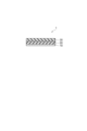
- FIG. 1 is a cross-sectional view that illustrates a photosensitive element according to an embodiment of the present invention.
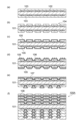
- 1A to 1C are schematic diagrams illustrating one aspect of a method for manufacturing a printed wiring board according to an embodiment of the present invention.
- process includes not only an independent process, but also a process that cannot be clearly distinguished from other processes as long as the intended effect of the process is achieved.
- layer includes a structure having a shape formed over the entire surface when observed in a plan view, as well as a structure having a shape formed on only a portion of the surface.
- a numerical range indicated using “ ⁇ ” indicates a range that includes the numerical values before and after " ⁇ " as the minimum and maximum values, respectively.
- the upper or lower limit of a numerical range in a certain stage may be replaced with the upper or lower limit of a numerical range in another stage, or may be replaced with a value shown in an example.
- the description "10 or more” means 10 and numerical values exceeding 10, and this also applies when the numerical values are different.
- the description "10 or less” means numerical values 10 and less than 10, and this also applies when the numerical values are different.
- the content of each component in the composition means the total content of the multiple substances present in the composition when the composition contains multiple substances corresponding to each component, unless otherwise specified.
- the "number of ring members” refers to the number of carbon atoms required to form a ring, and does not include the number of carbon atoms of the substituents on the ring.
- (meth)acrylate means at least one of “acrylate” and the corresponding “methacrylate”, and the same applies to other similar expressions such as (meth)acrylic acid.
- solid content refers to the non-volatile content excluding volatile substances contained in the photosensitive resin composition, and includes components that are liquid, syrup-like, or waxy at room temperature (around 25°C).
- the photosensitive resin composition contains (A) an acid-modified vinyl group-containing resin, (B) a photopolymerization initiator, (C) a photopolymerizable compound, and (D) a thermosetting resin.
- the (A) acid-modified vinyl group-containing resin contains a first resin having a weight average molecular weight of less than 4000 and a second resin having a weight average molecular weight of 4000 or more.
- the content of the (A) acid-modified vinyl group-containing resin is more than 60 mass% based on the total amount of the (A) acid-modified vinyl group-containing resin.
- the content of the (A) acid-modified vinyl group-containing resin is more than 33 mass% based on the total amount of the photosensitive resin composition.
- the photosensitive resin composition according to the present embodiment is a negative photosensitive resin composition having a total mass of 1000 to 2000 nm.
- the photosensitive resin composition according to the present embodiment is a negative photosensitive resin composition having a total mass of 1000 to 2000 nm.
- the photosensitive resin composition is a cured product, and the cured product of the photosensitive resin composition can be suitably used as a permanent resist for an interlayer insulating layer, etc.
- each component used in the photosensitive resin composition of the present embodiment will be described in more detail. do.
- the photosensitive resin composition according to the present embodiment contains an acid-modified vinyl group-containing resin as component (A).
- the acid-modified vinyl group-containing resin is not particularly limited as long as it has a vinyl group, which is a photopolymerizable ethylenically unsaturated bond, and an alkali-soluble acidic group.
- Examples of the acidic group contained in component (A) include a carboxy group, a sulfo group, and a phenolic hydroxyl group. Among these, a carboxy group is preferred from the viewpoint of superior resolution.
- acid-modified vinyl group-containing resin is acid-modified epoxy (meth)acrylate.
- Acid-modified epoxy (meth)acrylate is a resin obtained by acid-modifying epoxy (meth)acrylate, which is a reaction product of epoxy resin and organic acid having a vinyl group.
- An example of an acid-modified epoxy (meth)acrylate that can be used is an addition reaction product obtained by adding saturated or unsaturated polybasic acid anhydride (c) to an ester obtained by reacting epoxy resin (a) with vinyl group-containing monocarboxylic acid (b).
- epoxy resins (a) include bisphenol novolac type epoxy resins, novolac type epoxy resins, bisphenol A type epoxy resins, bisphenol F type epoxy resins, triphenol methane type epoxy resins, biphenyl type epoxy resins, naphthalene type epoxy resins, and dicyclopentadiene type epoxy resins.
- vinyl group-containing monocarboxylic acids (b) include (meth)acrylic acids or derivatives thereof, such as acrylic acid, acrylic acid dimers, methacrylic acid, ⁇ -furfurylacrylic acid, ⁇ -styrylacrylic acid, cinnamic acid, crotonic acid, and ⁇ -cyanocinnamic acid, half-ester compounds which are reaction products of hydroxyl group-containing (meth)acrylates and dibasic acid anhydrides, and half-ester compounds which are reaction products of vinyl group-containing monoglycidyl ethers or vinyl group-containing monoglycidyl esters and dibasic acid anhydrides.
- (meth)acrylic acids or derivatives thereof such as acrylic acid, acrylic acid dimers, methacrylic acid, ⁇ -furfurylacrylic acid, ⁇ -styrylacrylic acid, cinnamic acid, crotonic acid, and ⁇ -cyanocinnamic acid
- half-ester compounds which are
- hydroxyl group-containing (meth)acrylates examples include hydroxyethyl acrylate, hydroxyethyl methacrylate, hydroxypropyl acrylate, hydroxypropyl methacrylate, hydroxybutyl acrylate, hydroxybutyl methacrylate, polyethylene glycol monoacrylate, polyethylene glycol monomethacrylate, trimethylolpropane diacrylate, trimethylolpropane dimethacrylate, pentaerythritol triacrylate, pentaerythritol trimethacrylate, dipentaerythritol pentaacrylate, pentaerythritol pentamethacrylate, glycidyl acrylate, and glycidyl methacrylate.
- dibasic acid anhydrides examples include succinic anhydride, maleic anhydride, tetrahydrophthalic anhydride, phthalic anhydride, methyltetrahydrophthalic anhydride, ethyltetrahydrophthalic anhydride, hexahydrophthalic anhydride, methylhexahydrophthalic anhydride, ethylhexahydrophthalic anhydride, and itaconic anhydride.
- saturated or unsaturated polybasic acid anhydride (c) examples include succinic anhydride, maleic anhydride, tetrahydrophthalic anhydride, phthalic anhydride, methyltetrahydrophthalic anhydride, ethyltetrahydrophthalic anhydride, hexahydrophthalic anhydride, methylhexahydrophthalic anhydride, ethylhexahydrophthalic anhydride, and itaconic anhydride.
- tetrahydrophthalic anhydride may be used from the viewpoint of superior resolution.
- Examples of the acid-modified epoxy (meth)acrylate include (A1) an acid-modified epoxy (meth)acrylate having an alicyclic skeleton, and (A2) an acid-modified epoxy (meth)acrylate not having an alicyclic skeleton. From the viewpoints of achieving superior resolution, adhesion and electrical insulation reliability of the cured product, and further reducing residue at the bottom when forming a via, it is preferable that the (A) component contains the (A1) component.
- the number of ring members in the alicyclic skeleton of component (A1) is preferably 5 to 20, more preferably 5 to 18, even more preferably 6 to 18, particularly preferably 8 to 14, and extremely preferably 8 to 12, from the viewpoints of achieving superior resolution, adhesion of the cured product, and electrical insulation reliability, and further reducing residue at the bottom of via formation. From the same viewpoint, the number of rings in the alicyclic skeleton of component (A1) is preferably 2 or more, more preferably 2 to 4, and even more preferably 3.
- Examples of alicyclic skeletons with one ring include a cyclohexane skeleton and a cyclohexene skeleton, and examples of alicyclic skeletons with two or more rings include a norbornane skeleton, a decalin skeleton, a bicycloundecane skeleton, and a saturated dicyclopentadiene skeleton.
- the (A1) component preferably has a saturated dicyclopentadiene skeleton as the alicyclic skeleton, and more preferably has a saturated dicyclopentadiene skeleton represented by the following formula (a).
- R A1 represents an alkyl group having 1 to 12 carbon atoms
- m 1 is an integer of 0 to 6
- * represents a bonding site to another structure.
- Examples of the alkyl group having 1 to 12 carbon atoms represented by R A1 include a methyl group, an ethyl group, an n-propyl group, an isopropyl group, an n-butyl group, an isobutyl group, a t-butyl group, and an n-pentyl group.
- the alkyl group is preferably an alkyl group having 1 to 6 carbon atoms, more preferably an alkyl group having 1 to 3 carbon atoms, and even more preferably a methyl group.
- m1 is preferably an integer of 0 to 2, and more preferably 0.
- m1 is an integer of 2 to 6
- multiple R A1 may be the same or different.
- Multiple R A1 may be substituted on the same carbon atom or on different carbon atoms, to the extent possible.
- the (A1) component can be, for example, an addition reaction product obtained by reacting an epoxy resin (a1) having an alicyclic skeleton with a vinyl group-containing monocarboxylic acid (b) to obtain an ester, to which a saturated or unsaturated polybasic acid anhydride (c) is added.
- epoxy resin (a1) examples include glycidyl ether type, glycidyl amine type, and glycidyl ester type. Among these, the glycidyl ether type is preferred.
- epoxy resin (a1) an epoxy resin represented by the following formula (a1-1) or an epoxy resin having a structural unit represented by the following formula (a1-2) is preferred.
- R A1 and m 1 are the same as R A1 and m 1 in formula (a), R A2 represents an alkyl group having 1 to 12 carbon atoms, m 2 is an integer of 0 to 3, and n represents the number of structural units in parentheses and is 0 to 10.
- the alkyl group having 1 to 12 carbon atoms represented by R A2 may be an alkyl group listed as R A1 .
- m2 is preferably 0 or 1, and more preferably 0.
- n represents the average value of the mixture. n is preferably 2 to 10.
- R A1 and m 1 are the same as R A1 and m 1 in formula (a).
- epoxy resins (a1) include, for example, dicyclopentadiene-type epoxy resins such as XD-1000 (trade name, manufactured by Nippon Kayaku Co., Ltd.), EPICLON HP-7200L, EPICLON HP-7200, EPICLON HP-7200HH, and EPICLON HP-7200HHH (trade names, manufactured by DIC Corporation, "EPICLON” is a registered trademark).
- an addition reaction product obtained by adding a saturated or unsaturated polybasic acid anhydride (c) to an ester obtained by reacting an epoxy resin (a2) that does not have an alicyclic skeleton with a vinyl group-containing monocarboxylic acid (b) can be used.
- Examples of the epoxy resin (a2) include bisphenol-based epoxy resins such as bisphenol A type epoxy resins, bisphenol F type epoxy resins, and bisphenol S type epoxy resins; bisphenol-based novolac type epoxy resins such as bisphenol A novolac type epoxy resins and bisphenol F novolac type epoxy resins; phenol aralkyl type epoxy resins; stilbene type epoxy resins; naphthalene skeleton-containing epoxy resins such as naphthalene type epoxy resins, naphthol novolac type epoxy resins, naphthol type epoxy resins, naphthol aralkyl type epoxy resins, and naphthylene ether type epoxy resins; biphenyl type epoxy resins; biphenyl aralkyl type epoxy resins; xylylene type epoxy resins; dihydroanthracene type epoxy resins; and aliphatic chain epoxy resins.
- bisphenol-based novolac type epoxy resins are preferred, and bisphenol F novolac type epoxy resin
- the acid value of component (A) is not particularly limited. From the viewpoint of improving the solubility of the unexposed portion in an alkaline aqueous solution, the acid value of component (A) may be 30 mgKOH/g or more, 40 mgKOH/g or more, or 50 mgKOH/g or more. From the viewpoint of improving the electrical properties of the cured product, the acid value of component (A) may be 150 mgKOH/g or less, 120 mgKOH/g or less, or 100 mgKOH/g or less.
- the (A) component contains a first resin having a weight average molecular weight (Mw) of less than 4000 and a second resin having a weight average molecular weight (Mw) of 4000 or more.
- the first and second resins are selected from the above-mentioned (A) component so that their Mw satisfies the above-mentioned conditions.
- the first resin may be the above-mentioned (A1) component.
- the second resin may be the above-mentioned (A2) component.
- the Mw of the first resin may be 3500 or less, 3000 or less, 2500 or less, or 2000 or less from the viewpoint of further reducing residue at the bottom during via formation, and may be 500 or more or 1000 or more from the viewpoint of ensuring resolution during development.
- the Mw of the second resin may be 4500 or more, 5000 or more, 5500 or more, or 6000 or more from the viewpoint of superior adhesion of the cured product, and may be 100,000 or less, 50,000 or less, or 10,000 or less from the viewpoint of adjusting the varnish viscosity during application.
- the difference between the Mw of the first resin and the Mw of the second resin may be 1000 or more, 1500 or more, 2000 or more, 2500 or more, 3000 or more, 3500 or more, or 4000 or more from the viewpoint of further reducing residue at the bottom when the via is formed and achieving superior adhesion of the cured product, and may be 10000 or less, 9000 or less, 8000 or less, 7000 or less, or 6000 or less from the viewpoint of compatibility.
- the Mw of component (A) can be measured by gel permeation chromatography (GPC).
- Mw can be measured under the following GPC conditions, and the value converted using the calibration curve of standard polystyrene can be used as Mw.
- the calibration curve can be created using a 5-sample set of standard polystyrene ("PStQuick MP-H" and "PStQuick B", manufactured by Tosoh Corporation).
- GPC device High-speed GPC device "HCL-8320GPC" (manufactured by Tosoh Corporation)
- Detector Differential refractometer or UV detector (manufactured by Tosoh Corporation)
- Eluent tetrahydrofuran (THF) Measurement temperature: 40°C Flow rate: 0.35 mL/min Sample concentration: 10 mg/5 mL THF Injection volume: 20 ⁇ L
- the content of the first resin is more than 60% by mass based on the total amount of the (A) component.
- the content of the first resin may be 65% by mass or more, 68% by mass or more, or 70% by mass or more based on the total amount of the (A) component, and from the viewpoint of viscosity in the entire constituent composition, the content of the first resin may be 95% by mass or less, 90% by mass or less, 85% by mass or less, or 80% by mass or less based on the total amount of the (A) component.
- the content of the second resin is less than 40% by mass based on the total amount of the (A) component.
- the content of the second resin may be 5% by mass or more, 10% by mass or more, 15% by mass or more, or 20% by mass or more based on the total amount of the (A) component, and from the viewpoint of further reducing residue at the bottom when the via is formed, the content of the second resin may be 35% by mass or less, 32% by mass or less, or 30% by mass or less based on the total amount of the (A) component.
- the content of component (A) in the photosensitive resin composition is 33% by mass or less based on the total solid content of the photosensitive resin composition. From the viewpoint of further reducing residue at the bottom during via formation, the content of component (A) may be 32% by mass or less, 31% by mass or less, 30% by mass or less, or 29% by mass or less based on the total solid content of the photosensitive resin composition, and from the viewpoint of ensuring resolution during development, the content of component (A) may be 20% by mass or more, 22% by mass or more, or 25% by mass or more based on the total solid content of the photosensitive resin composition.
- the photosensitive resin composition according to the present embodiment contains a photopolymerization initiator as component (B).
- the component (B) is not particularly limited as long as it can polymerize the component (A) and the like.
- component (B) examples include benzoin compounds such as benzoin, benzoin methyl ether, and benzoin isopropyl ether; acetophenone compounds such as acetophenone, 2,2-dimethoxy-2-phenylacetophenone, 2,2-diethoxy-2-phenylacetophenone, 1,1-dichloroacetophenone, 1-hydroxycyclohexyl phenyl ketone, 2-benzyl-2-dimethylamino-1-(4-morpholinophenyl)-1-butanone, 2-methyl-[4-(methylthio)phenyl]-2-morpholino-1-propane, and N,N-dimethylaminoacetophenone; 2-methylanthraquinone, 2-ethylanthraquinone, and 2-tert-butyl anthraquinone.
- benzoin compounds such as benzoin, benzoin methyl ether, and benzoin isopropyl ether
- anthraquinone compounds such as anthraquinone, 1-chloroanthraquinone, 2-amyl anthraquinone, and 2-amino anthraquinone
- thioxanthone compounds such as 2,4-dimethylthioxanthone, 2,4-diethylthioxanthone, 2-chlorothioxanthone, and 2,4-diisopropylthioxanthone
- ketal compounds such as acetophenone dimethyl ketal and benzyl dimethyl ketal
- benzophenone compounds such as benzophenone, methylbenzophenone, 4,4'-dichlorobenzophenone, 4,4'-bis(diethylamino)benzophenone, Michler's ketone, and 4-benzoyl-4'-methyldiphenyl sulfide
- 2-(o-chlorophenyl)-4,5-diphenone Imidazole compounds such as
- the (B) component may be used alone or in combination of two or more.
- the content of component (B) in the photosensitive resin composition is not particularly limited, but may be 0.1 to 15 mass%, 0.15 to 5 mass%, 0.15 to 1.5 mass%, or 0.18 to 1.2 mass% based on the total solid content of the photosensitive resin composition.
- the content of component (B) is 0.1 mass% or more, there is a tendency to easily suppress elution of exposed areas during development when forming a resist pattern, and when the content of component (B) is 15 mass% or less, there is a tendency to easily improve the heat resistance of the cured product.
- the photosensitive resin composition according to the present embodiment includes, as the component (C), a photopolymerizable compound from the viewpoint of increasing the chemical resistance after exposure and increasing the difference in developer resistance between the exposed area and the unexposed area.
- the component (C) is not particularly limited as long as it is a photopolymerizable compound that has an ethylenically unsaturated group and does not have an acidic group.
- component (C) examples include photopolymerizable compounds having one ethylenically unsaturated group, photopolymerizable compounds having two ethylenically unsaturated groups, and photopolymerizable compounds having three or more ethylenically unsaturated groups.
- Examples of photopolymerizable compounds having one ethylenically unsaturated group include (meth)acrylic acid and (meth)acrylic acid alkyl esters.
- Examples of (meth)acrylic acid alkyl esters include (meth)acrylic acid methyl ester, (meth)acrylic acid ethyl ester, (meth)acrylic acid butyl ester, (meth)acrylic acid 2-ethylhexyl ester, and (meth)acrylic acid hydroxyethyl ester.
- photopolymerizable compounds having two ethylenically unsaturated groups include polyethylene glycol di(meth)acrylate, trimethylolpropane di(meth)acrylate, polypropylene glycol di(meth)acrylate, 2,2-bis(4-(meth)acryloxypolyethoxypolypropoxyphenyl)propane, and bisphenol A diglycidyl ether di(meth)acrylate.
- photopolymerizable compounds having three or more ethylenically unsaturated groups include (meth)acrylate compounds having a skeleton derived from trimethylolpropane, such as trimethylolpropane tri(meth)acrylate; (meth)acrylate compounds having a skeleton derived from tetramethylolmethane, such as tetramethylolmethane tri(meth)acrylate and tetramethylolmethane tetra(meth)acrylate; (meth)acrylate compounds having a skeleton derived from pentaerythritol, such as pentaerythritol tri(meth)acrylate and pentaerythritol tetra(meth)acrylate; (meth)acrylate compounds having a skeleton derived from dipentaerythritol, such as dipentaerythritol penta(meth)acrylate and dipentaerythritol
- (meth)acrylate compounds having a skeleton derived from dipentaerythritol are preferred, and dipentaerythritol penta(meth)acrylate and dipentaerythritol hexa(meth)acrylate are more preferred.
- the content may be 1 to 20 mass%, 2 to 15 mass%, or 4 to 12 mass% based on the total solid content of the photosensitive resin composition.
- thermosetting resin thermosetting resin
- the photosensitive resin composition according to the present embodiment contains a thermosetting resin as component (D). By containing component (D), a cured product having excellent adhesive properties can be formed.
- the ) components may be used alone or in combination of two or more.
- component (D) examples include epoxy resins, phenolic resins, unsaturated imide resins, cyanate resins, isocyanate resins, benzoxazine resins, oxetane resins, amino resins, unsaturated polyester resins, allyl resins, dicyclopentadiene resins, silicone resins, triazine resins, and melamine resins.
- epoxy resins are preferred from the viewpoint of superior adhesion of the cured product.
- Epoxy resins include, for example, bisphenol-type epoxy resins such as bisphenol A-type epoxy resins, bisphenol F-type epoxy resins, and bisphenol S-type epoxy resins; novolac-type epoxy resins such as bisphenol-based novolac-type epoxy resins, phenol novolac-type epoxy resins, cresol novolac-type epoxy resins, and biphenyl novolac-type epoxy resins; phenol aralkyl-type epoxy resins; stilbene-type epoxy resins; naphthalene-skeleton-containing epoxy resins such as naphthalene-type epoxy resins, naphthol novolac-type epoxy resins, naphthol-type epoxy resins, naphthol aralkyl-type epoxy resins, and naphthylene ether-type epoxy resins; biphenyl-type epoxy resins; biphenyl aralkyl-type epoxy resins; xylylene-type epoxy resins; dihydroanthracene-type epoxy resin
- At least one type of epoxy resin selected from bisphenol type epoxy resin, phenol novolac type epoxy resin, naphthol type epoxy resin, naphthalene type epoxy resin, biphenyl type epoxy resin, naphthylene ether type epoxy resin, and cresol novolac type epoxy resin, from the viewpoint of obtaining a cured product with excellent heat resistance, adhesiveness, and electrical insulation reliability, and further reducing residue at the bottom of vias when they are formed.
- the content of component (D) in the photosensitive resin composition may be 2 to 30 mass%, 5 to 25 mass%, or 8 to 20 mass% based on the total solid content of the photosensitive resin composition.
- the content of component (D) is within the above range, the heat resistance of the formed cured film can be further improved while maintaining good developability.
- the photosensitive resin composition according to the present embodiment may further contain an inorganic filler as component (E).
- component (E) By containing component (E), the adhesiveness, reliability, etc. of the cured product can be improved.
- the component (E) may be used alone or in combination of two or more.
- inorganic fillers include silica, alumina, titania, tantalum oxide, zirconia, silicon nitride, barium titanate, barium carbonate, magnesium carbonate, aluminum hydroxide, magnesium hydroxide, lead titanate, lead zirconate titanate, lead lanthanum zirconate titanate, gallium oxide, spinel, mullite, cordierite, talc, aluminum titanate, yttria-containing zirconia, barium silicate, boron nitride, calcium carbonate, barium sulfate, calcium sulfate, zinc oxide, magnesium titanate, hydrotalcite, mica, calcined kaolin, and carbon.
- Component (E) may contain silica to improve the heat resistance of the cured product, and may contain barium sulfate to improve the heat resistance and adhesiveness of the cured product.
- an inorganic filler that has been surface-treated with alumina or an organosilane compound may be used.
- the average particle size of the inorganic filler is preferably 0.01 to 5.0 ⁇ m, more preferably 0.1 to 3.0 ⁇ m, even more preferably 0.3 to 2.0 ⁇ m, and particularly preferably 0.5 to 1.5 ⁇ m.
- the content may be 5 to 80 mass%, 10 to 60 mass%, 15 to 50 mass%, 20 to 45 mass%, 25 to 40 mass%, or 30 to 40 mass% based on the total solid content of the photosensitive resin composition.
- the content of component (E) is within the above range, the resolution, mechanical strength and heat resistance of the cured product, etc. can be improved.
- the photosensitive resin composition of the present embodiment may further contain a pigment as component (F) from the viewpoint of improving the distinguishability or appearance of the manufacturing device.
- a pigment as component (F)
- a colorant that develops a desired color when concealing wiring, etc. can be used.
- component (F) include phthalocyanine blue, phthalocyanine green, iodine green, diazo yellow, crystal violet, titanium oxide, carbon black, and naphthalene black.
- the content of component (F) may be 0.1 to 10 mass%, 0.5 to 8 mass%, or 1 to 5 mass% based on the total solid content in the photosensitive resin composition, from the viewpoint of further concealing the wiring.
- the photosensitive resin composition according to this embodiment may further contain an elastomer as component (G).
- component (G) By containing component (G), it is possible to suppress the decrease in flexibility and adhesive strength caused by strain (internal stress) inside the resin due to the cure shrinkage of component (A).
- component (G) By containing component (G), the resolution of the photosensitive resin composition, the adhesiveness of the cured product, and the electrical insulation reliability tend to be improved.
- the component (G) may be used alone or in combination of two or more.
- Examples of the (G) component include styrene-based elastomers, olefin-based elastomers, urethane-based elastomers, polyester-based elastomers, polyamide-based elastomers, acrylic-based elastomers, and silicone-based elastomers. These elastomers are composed of hard segment components that contribute to heat resistance and strength, and soft segment components that contribute to flexibility and toughness.
- styrene-based elastomers examples include styrene-butadiene-styrene block copolymers, styrene-isoprene-styrene block copolymers, styrene-ethylene-butylene-styrene block copolymers, and styrene-ethylene-propylene-styrene block copolymers.
- styrene derivatives such as ⁇ -methylstyrene, 3-methylstyrene, 4-propylstyrene, and 4-cyclohexylstyrene can be used as components that make up styrene-based elastomers.
- the number average molecular weight of the styrene-based elastomer may be 1,000 to 50,000 or 3,000 to 20,000.
- the number average molecular weight is a value calculated in terms of standard polystyrene by gel permeation chromatography (GPC) using tetrahydrofuran as a solvent.
- olefin-based elastomers include polymers or copolymers of ⁇ -olefins having 2 to 20 carbon atoms, such as ethylene, propylene, 1-butene, 1-hexene, and 4-methyl-pentene; copolymers of ⁇ -olefins having 2 to 20 carbon atoms and non-conjugated dienes having 2 to 20 carbon atoms, such as dicyclopentadiene, 1,4-hexadiene, cyclooctadiene, methylenenorbornene, ethylidenenorbornene, butadiene, and isoprene; and carboxylic acid-modified butadiene-acrylonitrile copolymers.
- polyethylene polyethylene, polybutadiene, hydroxyl-containing polybutadiene, hydroxyl-containing polyisopropylene, ethylene-propylene copolymer (EPR), and ethylene-propylene-diene copolymer (EPDM).
- EPR ethylene-propylene copolymer
- EPDM ethylene-propylene-diene copolymer
- the number average molecular weight of the olefin-based elastomer may be 1,000 to 8,000 or 1,500 to 6,500.
- polyester-based elastomer a compound obtained by polycondensation of a dicarboxylic acid or its derivative with a diol compound or its derivative can be used.
- Dicarboxylic acids include, for example, aromatic dicarboxylic acids such as terephthalic acid, isophthalic acid, and naphthalenedicarboxylic acid; aliphatic dicarboxylic acids having 2 to 20 carbon atoms such as adipic acid, sebacic acid, and dodecanedicarboxylic acid; and alicyclic dicarboxylic acids such as cyclohexanedicarboxylic acid.
- Diol compounds include, for example, aliphatic diols such as ethylene glycol, 1,3-propanediol, 1,4-butanediol, 1,6-hexanediol, and 1,10-decanediol; alicyclic diols such as 1,4-cyclohexanediol; and aromatic diols such as bisphenol A, bis(4-hydroxyphenyl)methane, bis(4-hydroxy-3-methylphenyl)propane, and resorcinol.
- aliphatic diols such as ethylene glycol, 1,3-propanediol, 1,4-butanediol, 1,6-hexanediol, and 1,10-decanediol
- alicyclic diols such as 1,4-cyclohexanediol
- aromatic diols such as bisphenol A, bis(4-hydroxyphenyl)methan
- polyester-based elastomer a multiblock copolymer in which an aromatic polyester (e.g., polybutylene terephthalate) is used as the hard segment component and an aliphatic polyester (e.g., polytetramethylene glycol) is used as the soft segment component.
- aromatic polyester e.g., polybutylene terephthalate
- aliphatic polyester e.g., polytetramethylene glycol
- polyester-based elastomers There are various grades of polyester-based elastomers depending on the type, ratio, and molecular weight of the hard and soft segments.
- the number average molecular weight of the polyester elastomer may be 900 to 30,000, 1,000 to 25,000, or 5,000 to 20,000.
- a compound composed of a hard segment made of a low molecular weight (short chain) diol and diisocyanate, and a soft segment made of a high molecular weight (long chain) diol and diisocyanate can be used.
- short-chain diols examples include ethylene glycol, propylene glycol, 1,4-butanediol, and bisphenol A.
- the number average molecular weight of the short-chain diol is preferably 48 to 500.
- long-chain diols examples include polypropylene glycol, polytetramethylene oxide, poly(1,4-butylene adipate), poly(ethylene-1,4-butylene adipate), polycaprolactone, poly(1,6-hexylene carbonate), and poly(1,6-hexylene-neopentylene adipate).
- the number average molecular weight of the long-chain diol is preferably 500 to 10,000.
- the number average molecular weight of the urethane elastomer may be 1,000 to 25,000, 1,500 to 20,000, or 2,000 to 15,000.
- Polyamide elastomers are broadly divided into two types: polyether block amide type and polyether ester block amide type, which use polyamide for the hard segment and polyether or polyester for the soft segment.
- polyamides include polyamide-6, polyamide-11, and polyamide-12.
- polyethers include polyoxyethylene glycol, polyoxypropylene glycol, and polytetramethylene glycol.
- the number average molecular weight of the polyamide elastomer may be 1,000 to 50,000 or 2,000 to 30,000.
- the acrylic elastomer may be a compound containing a structural unit based on a (meth)acrylic acid ester as the main component.
- (meth)acrylic acid esters include methyl (meth)acrylate, ethyl (meth)acrylate, butyl (meth)acrylate, methoxyethyl (meth)acrylate, and ethoxyethyl (meth)acrylate.
- the acrylic elastomer may be a compound obtained by copolymerizing a (meth)acrylic acid ester with acrylonitrile, or may be a compound obtained by further copolymerizing a monomer having a functional group that serves as a crosslinking point. Examples of monomers having a functional group include glycidyl methacrylate and allyl glycidyl ether.
- acrylic elastomers examples include acrylonitrile-butyl acrylate copolymer, acrylonitrile-butyl acrylate-ethyl acrylate copolymer, methyl methacrylate-butyl acrylate-methacrylic acid copolymer, and acrylonitrile-butyl acrylate-glycidyl methacrylate copolymer.
- the number average molecular weight of the acrylic elastomer may be 1,000 to 50,000 or 2,000 to 30,000.
- a silicone-based elastomer is a compound whose main component is organopolysiloxane.
- organopolysiloxane examples include polydimethylsiloxane, polymethylphenylsiloxane, and polydiphenylsiloxane.
- a silicone-based elastomer may be a compound in which part of an organopolysiloxane is modified with a vinyl group, an alkoxy group, or the like.
- the number average molecular weight of the silicone elastomer may be 1,000 to 50,000 or 2,000 to 30,000.
- component (G) contains at least one selected from the group consisting of olefin-based elastomers, polyester-based elastomers, and urethane-based elastomers, and it is more preferable that component (G) contains a polyester-based elastomer. From the same viewpoint, it is preferable that component (G) is an elastomer that is liquid at room temperature.
- the content may be 0.5 to 20 mass%, 0.5 to 15 mass%, 0.5 to 10 mass%, 1.0 to 6 mass%, or 1.0 to 4.0 mass% based on the total solid content of the photosensitive resin composition.
- the content of component (G) is within the above range, the resolution, adhesion of the cured product, and electrical insulation reliability tend to be superior.
- the photosensitive resin composition according to the present embodiment may further contain various additives as necessary.
- the additives include thermal polymerization initiators; polymerization inhibitors such as hydroquinone, methylhydroquinone, hydroquinone monomethyl ether, catechol, and pyrogallol; thickeners such as bentone and montmorillonite; antifoaming agents such as silicone-based, fluorine-based, and vinyl resin-based; silane coupling agents; flame retardants such as brominated epoxy compounds, acid-modified brominated epoxy compounds, antimony compounds, phosphate compounds, aromatic condensed phosphate esters, and halogen-containing condensed phosphate esters; and thermoplastic resins such as polyester polyurethane resins.
- the photosensitive resin composition according to the present embodiment may contain a solvent as necessary.
- the photosensitive resin composition according to the present embodiment contains a solvent for dissolving and dispersing each component, which makes it easy to apply the composition onto a substrate and allows a coating film of uniform thickness to be formed, thereby allowing a more precise pattern to be formed.
- the solvent examples include organic solvents.
- the organic solvent include ketones such as methyl ethyl ketone and cyclohexanone; aromatic hydrocarbons such as toluene, xylene, and tetramethylbenzene; glycol ethers such as methyl cellosolve, butyl cellosolve, methyl carbitol, butyl carbitol, propylene glycol monomethyl ether, dipropylene glycol monoethyl ether, dipropylene glycol diethyl ether, and triethylene glycol monoethyl ether; esters such as ethyl acetate, butyl acetate, propylene glycol monoethyl ether acetate, butyl cellosolve acetate, and carbitol acetate; aliphatic hydrocarbons such as octane and decane; and petroleum-based solvents such as petroleum ether, petroleum naphtha, hydrogenated petroleum naphtha, and
- the amount of solvent to be added may be appropriately selected so that the total solids concentration in the photosensitive resin composition is 40 to 90% by mass, 45 to 80% by mass, or 45 to 70% by mass.
- the photosensitive resin composition of this embodiment can be prepared by uniformly mixing the above-mentioned components using a roll mill, a bead mill, or the like.
- the photosensitive resin composition of this embodiment may be used in a liquid state, or in a film state, such as the photosensitive element described below.
- the photosensitive element according to this embodiment includes a support film and a photosensitive layer containing the above-mentioned photosensitive resin composition.
- Fig. 1 is a cross-sectional view showing a schematic diagram of the photosensitive element according to this embodiment. As shown in Fig. 1, the photosensitive element 1 includes a support film 10 and a photosensitive layer 20 formed on the support film 10. The photosensitive element 1 may further include a protective film 30 on the photosensitive layer 20.
- the photosensitive element 1 can be produced by applying the photosensitive resin composition according to this embodiment onto a support film 10 using a known coating device such as a comma coater, bar coater, kiss coater, roll coater, gravure coater, or die coater, and then drying the coating to form a photosensitive layer 20.
- a known coating device such as a comma coater, bar coater, kiss coater, roll coater, gravure coater, or die coater, and then drying the coating to form a photosensitive layer 20.
- the thickness of the photosensitive layer is not particularly limited, but may be 1 to 100 ⁇ m, 1 to 50 ⁇ m, or 5 to 40 ⁇ m from the viewpoint of making the printed wiring board thinner.
- the coating film can be dried using a hot air dryer, a dryer using far-infrared rays or near-infrared rays, etc.
- the drying temperature may be 60 to 150°C, 70 to 120°C, or 80 to 100°C.
- the drying time may be 1 to 60 minutes, 2 to 30 minutes, or 5 to 20 minutes.
- the content of residual solvent in the coating film after drying may be 3% by mass or less, 2% by mass or less, or 1% by mass or less, from the viewpoint of avoiding diffusion of the solvent during the manufacturing process of the printed wiring board.
- the support film examples include polyester films such as polyethylene terephthalate film and polybutylene terephthalate film; and polyolefin films such as polypropylene film and polyethylene film.
- the thickness of the support film may be, for example, 5 to 100 ⁇ m, 5 to 60 ⁇ m, or 15 to 45 ⁇ m.
- the protective film 30 may be, for example, a polymer film such as polyethylene or polypropylene.
- the protective film 30 may be the same as the support film 10, or a different film.
- the photosensitive resin composition according to this embodiment is suitable as a permanent resist for the interlayer insulating layer of a printed wiring board, etc.
- the photosensitive resin composition according to this embodiment is also useful for forming a cavity for incorporating a chip or a passive element, etc.
- the photosensitive resin composition according to this embodiment is also useful for forming a surface protection layer for a printed wiring board.
- the printed wiring board according to this embodiment includes an interlayer insulating layer that contains a cured product of the photosensitive resin composition according to this embodiment.
- the method for manufacturing a printed wiring board according to this embodiment includes the steps of forming a photosensitive layer on a substrate using the photosensitive resin composition or photosensitive element according to this embodiment, exposing and developing the photosensitive layer to form a resist pattern, and curing the resist pattern to form an interlayer insulating layer.
- FIG. 2 is a schematic cross-sectional view showing an example of a method for manufacturing a multilayer printed wiring board having an interlayer insulating layer made of a cured product of the photosensitive resin composition according to this embodiment.
- Multilayer printed wiring board 100A shown in FIG. 2(f) has a wiring pattern on the surface and inside.
- Multilayer printed wiring board 100A can be obtained by laminating a copper clad laminate, an interlayer insulating layer, a metal foil, etc., and appropriately forming a wiring pattern by an etching method or a semi-additive method. Below, the method for manufacturing multilayer printed wiring board 100A will be briefly described based on FIG. 2.
- interlayer insulating layers 103 are formed on both sides of a substrate (e.g., a copper-clad laminate) 101 having a wiring pattern 102 on its surface (see FIG. 2(a)).
- the interlayer insulating layer 103 may be formed by printing the photosensitive resin composition according to this embodiment using a screen printer or roll coater, or it may be formed by preparing a photosensitive element according to this embodiment in advance and attaching the photosensitive layer of the photosensitive element to the surface of the substrate 101 using a laminator.
- a YAG laser or a carbon dioxide laser is used to form vias (openings) 104 in areas that require electrical connection to the outside (see FIG. 2(b)). Smears (residues) around the vias 104 can be removed by a desmear process.
- a seed layer 105 is formed by electroless plating (see FIG. 2(c)).
- a photosensitive layer containing a photosensitive resin composition is formed on the seed layer 105, and predetermined locations are exposed and developed to form a resin pattern 106 (see FIG. 2(d)).
- the wiring pattern 107 is formed by electrolytic plating in the portion of the seed layer 105 where the resin pattern 106 is not formed. Then, the resin pattern 106 is removed by a stripping liquid, and the portion of the seed layer 105 where the wiring pattern 107 is not formed is removed by etching (see FIG. 2(e)).
- the above operations are repeated to form a solder resist 108 containing a cured product of the photosensitive resin composition according to this embodiment on the outermost surface, thereby producing a multilayer printed wiring board 100A (see FIG. 2(f)).
- the multilayer printed wiring board 100A thus obtained can have, for example, semiconductor elements mounted in corresponding locations, ensuring electrical connections.
- the photosensitive resin composition according to this embodiment can be used to produce a semiconductor element having an interlayer insulating layer formed from the cured product of the above-mentioned photosensitive resin composition, and an electronic device including the semiconductor element.
- the semiconductor element may be, for example, a memory, package, etc. having a multilayer wiring structure, a rewiring structure, etc.
- Examples of electronic devices include mobile phones, smartphones, tablet terminals, personal computers, and hard disk suspensions.
- B-1 2-methyl-[4-(methylthio)phenyl]-2-morpholino-1-propane (manufactured by IGM Resins B.V., trade name "Omnirad 907")
- B-2 2,4-diethylthioxanthone (manufactured by Nagase & Co., Ltd., product name "SB-PI799")
- C-1 Dipentaerythritol hexaacrylate (manufactured by Nippon Kayaku Co., Ltd., product name "DPHA”)
- D-2 Dicyclopentanyl acrylate (manufactured by Resonac Corporation, product name "FA-513AS”)
- D-1 Bisphenol novolac type epoxy resin (manufactured by Nippon Kayaku Co., Ltd., product name "RE-306”)
- D-2 Tetramethylbiphenol type epoxy resin (manufactured by Mitsubishi Chemical Corporation, product name "YX4
- Photosensitive resin composition The components were mixed in the amounts (parts by weight, solid content equivalent) shown in Table 1 and kneaded in a three-roll mill. Carbitol acetate was then added so that the solid content concentration became 60% by weight, and the mixture was sensitized. A polymerizable resin composition was prepared.
- a polyethylene terephthalate film (manufactured by Teijin Limited, product name "G2-16") having a thickness of 16 ⁇ m was prepared as a support film.
- the photosensitive resin composition was applied onto the support film so that the thickness after drying would be 18 ⁇ m, and dried at 75° C. for 30 minutes using a hot air convection dryer to form a photosensitive layer.
- a polyethylene film (manufactured by Tamapoly Corporation, product name "NF-15”) was attached as a protective film to the surface of the photosensitive layer opposite to the side in contact with the support film, to obtain a photosensitive element.
- a copper-clad laminate substrate (manufactured by Resonac Co., Ltd., product name "MCL-E-67”) having a thickness of 0.6 mm was prepared. While peeling and removing the protective film from the photosensitive element, a photosensitive layer was laminated on the copper-clad laminate substrate using a press-type vacuum laminator (manufactured by Meiki Seisakusho Co., Ltd., product name "MVLP-500”) under the following conditions: pressure bonding pressure: 0.4 MPa, press hot plate temperature: 80°C, vacuum drawing time: 25 seconds, lamination press time: 25 seconds, and atmospheric pressure: 4 kPa or less, to obtain a laminate.
- a press-type vacuum laminator manufactured by Meiki Seisakusho Co., Ltd., product name "MVLP-500
- the photosensitive layer was exposed to light using an i-line exposure device (manufactured by Ushio Co., Ltd., product name "UX-2240SM-XJ-01") through a negative mask having a via pattern with an opening diameter of 30 ⁇ m, while changing the exposure light in increments of 50 mJ/ cm2 in the range of 100 to 1000 mJ/ cm2 .
- the unexposed portion was dissolved and developed by spray development at a pressure of 1.765 ⁇ 10 5 Pa for a time equivalent to 2.5 times the shortest development time (the shortest time for removing the unexposed portion of the photosensitive layer) at 30° C. using a 1% by mass aqueous sodium carbonate solution.
- the unexposed portion was dissolved and developed by exposing the substrate to an exposure dose of 2000 mJ/cm 2 using an ultraviolet exposure device to prepare a test piece having a cured film on a copper-clad laminate substrate with a via pattern having an opening diameter of 30 ⁇ m.
- the above test piece was checked with a scanning electron microscope for the presence or absence of residue at the bottom of the via pattern portion. Evaluation was performed according to the following criteria. The results are shown in Table 1. ⁇ Evaluation criteria> A: No residue was found on the bottom. B: Residue was observed in part of the bottom. C: Residue was observed over the entire bottom surface.
- Reference Signs List 1 photosensitive element, 10: support film, 20: photosensitive layer, 30: protective film, 100A: multilayer printed wiring board, 101: substrate, 102, 107: wiring pattern, 103: interlayer insulating layer, 104: via, 105: seed layer, 106: resin pattern, 108: solder resist.
Landscapes
- Physics & Mathematics (AREA)
- Engineering & Computer Science (AREA)
- General Physics & Mathematics (AREA)
- Spectroscopy & Molecular Physics (AREA)
- Chemical & Material Sciences (AREA)
- Manufacturing & Machinery (AREA)
- Microelectronics & Electronic Packaging (AREA)
- Chemical Kinetics & Catalysis (AREA)
- Inorganic Chemistry (AREA)
- Architecture (AREA)
- Structural Engineering (AREA)
- Health & Medical Sciences (AREA)
- Medicinal Chemistry (AREA)
- Polymers & Plastics (AREA)
- Organic Chemistry (AREA)
- General Chemical & Material Sciences (AREA)
- Materials For Photolithography (AREA)
- Macromonomer-Based Addition Polymer (AREA)
Priority Applications (4)
| Application Number | Priority Date | Filing Date | Title |
|---|---|---|---|
| CN202480002247.9A CN119072658A (zh) | 2023-02-06 | 2024-01-31 | 感光性树脂组合物、感光性元件、印刷线路板及印刷线路板的制造方法 |
| US18/859,085 US20250362600A1 (en) | 2023-02-06 | 2024-01-31 | Photosensitive resin composition, photosensitive element, printed wiring board, and method for manufacturing printed wiring board |
| KR1020257016274A KR20250144986A (ko) | 2023-02-06 | 2024-01-31 | 감광성 수지 조성물, 감광성 엘리먼트, 프린트 배선판, 및 프린트 배선판의 제조 방법 |
| JP2024576269A JPWO2024166766A1 (https=) | 2023-02-06 | 2024-01-31 |
Applications Claiming Priority (2)
| Application Number | Priority Date | Filing Date | Title |
|---|---|---|---|
| JP2023016093 | 2023-02-06 | ||
| JP2023-016093 | 2023-02-06 |
Publications (1)
| Publication Number | Publication Date |
|---|---|
| WO2024166766A1 true WO2024166766A1 (ja) | 2024-08-15 |
Family
ID=92262483
Family Applications (1)
| Application Number | Title | Priority Date | Filing Date |
|---|---|---|---|
| PCT/JP2024/003089 Ceased WO2024166766A1 (ja) | 2023-02-06 | 2024-01-31 | 感光性樹脂組成物、感光性エレメント、プリント配線板、及びプリント配線板の製造方法 |
Country Status (6)
| Country | Link |
|---|---|
| US (1) | US20250362600A1 (https=) |
| JP (1) | JPWO2024166766A1 (https=) |
| KR (1) | KR20250144986A (https=) |
| CN (1) | CN119072658A (https=) |
| TW (1) | TW202432620A (https=) |
| WO (1) | WO2024166766A1 (https=) |
Citations (2)
| Publication number | Priority date | Publication date | Assignee | Title |
|---|---|---|---|---|
| JP2015021997A (ja) * | 2013-07-16 | 2015-02-02 | 互応化学工業株式会社 | 感光性樹脂及びソルダーレジスト用樹脂組成物 |
| WO2018225441A1 (ja) * | 2017-06-09 | 2018-12-13 | 互応化学工業株式会社 | 感光性樹脂組成物、ドライフィルム、及びプリント配線板 |
Family Cites Families (2)
| Publication number | Priority date | Publication date | Assignee | Title |
|---|---|---|---|---|
| JP7018168B2 (ja) | 2015-12-22 | 2022-02-10 | 昭和電工マテリアルズ株式会社 | 感光性樹脂組成物、それを用いたドライフィルム、プリント配線板、及びプリント配線板の製造方法 |
| JP2019066793A (ja) | 2017-10-05 | 2019-04-25 | 日立化成株式会社 | 感光性樹脂組成物、感光性エレメント及びプリント配線板 |
-
2024
- 2024-01-31 KR KR1020257016274A patent/KR20250144986A/ko active Pending
- 2024-01-31 JP JP2024576269A patent/JPWO2024166766A1/ja active Pending
- 2024-01-31 US US18/859,085 patent/US20250362600A1/en active Pending
- 2024-01-31 WO PCT/JP2024/003089 patent/WO2024166766A1/ja not_active Ceased
- 2024-01-31 CN CN202480002247.9A patent/CN119072658A/zh active Pending
- 2024-02-02 TW TW113104181A patent/TW202432620A/zh unknown
Patent Citations (2)
| Publication number | Priority date | Publication date | Assignee | Title |
|---|---|---|---|---|
| JP2015021997A (ja) * | 2013-07-16 | 2015-02-02 | 互応化学工業株式会社 | 感光性樹脂及びソルダーレジスト用樹脂組成物 |
| WO2018225441A1 (ja) * | 2017-06-09 | 2018-12-13 | 互応化学工業株式会社 | 感光性樹脂組成物、ドライフィルム、及びプリント配線板 |
Also Published As
| Publication number | Publication date |
|---|---|
| CN119072658A (zh) | 2024-12-03 |
| KR20250144986A (ko) | 2025-10-13 |
| JPWO2024166766A1 (https=) | 2024-08-15 |
| TW202432620A (zh) | 2024-08-16 |
| US20250362600A1 (en) | 2025-11-27 |
Similar Documents
| Publication | Publication Date | Title |
|---|---|---|
| TWI751601B (zh) | 感光性黏著劑組成物、乾膜、及多層基板的製造方法 | |
| TWI902694B (zh) | 感光性樹脂組成物、感光性樹脂薄膜、多層印刷線路板及半導體封裝體、以及多層印刷線路板的製造方法 | |
| JP2025175070A (ja) | 感光性樹脂組成物、感光性エレメント、プリント配線板、及びプリント配線板の製造方法 | |
| CN113614131A (zh) | 感光性树脂组合物、感光性树脂膜、印刷配线板和半导体封装体、以及印刷配线板的制造方法 | |
| JP2025142001A (ja) | 感光性樹脂組成物、感光性エレメント、プリント配線板、及びプリント配線板の製造方法 | |
| WO2024166766A1 (ja) | 感光性樹脂組成物、感光性エレメント、プリント配線板、及びプリント配線板の製造方法 | |
| KR20250005161A (ko) | 감광성 수지 조성물, 감광성 엘리먼트, 프린트 배선판, 및 프린트 배선판의 제조 방법 | |
| KR102893888B1 (ko) | 감광성 수지 조성물, 감광성 엘리먼트, 프린트 배선판, 및 프린트 배선판의 제조 방법 | |
| JP7729386B2 (ja) | 感光性樹脂組成物、感光性エレメント、プリント配線板、及びプリント配線板の製造方法 | |
| JP2025098756A (ja) | 感光性樹脂組成物、感光性エレメント、プリント配線板及びその製造方法、並びに、酸変性ビニル基含有樹脂 | |
| JP2025115748A (ja) | 感光性樹脂組成物、感光性エレメント、プリント配線板、及びプリント配線板の製造方法 | |
| JP2025098759A (ja) | 感光性樹脂組成物、感光性エレメント、プリント配線板及びその製造方法 | |
| WO2023140289A1 (ja) | 感光性樹脂組成物、感光性エレメント、プリント配線板、及びプリント配線板の製造方法 | |
| WO2025173119A1 (ja) | 絶縁フィルム | |
| WO2025262762A1 (ja) | 感光性樹脂組成物、感光性エレメント、及びプリント配線板 | |
| TW202605084A (zh) | 感光性樹脂組成物、感光性元件及印刷線路板 | |
| WO2024209640A1 (ja) | 感光性樹脂組成物、感光性エレメント、プリント配線板、及びプリント配線板の製造方法 | |
| WO2025204593A1 (ja) | 硬化性樹脂組成物、ドライフィルム、硬化物および電子部品 |
Legal Events
| Date | Code | Title | Description |
|---|---|---|---|
| 121 | Ep: the epo has been informed by wipo that ep was designated in this application |
Ref document number: 24753209 Country of ref document: EP Kind code of ref document: A1 |
|
| WWE | Wipo information: entry into national phase |
Ref document number: 202480002247.9 Country of ref document: CN |
|
| WWE | Wipo information: entry into national phase |
Ref document number: 18859085 Country of ref document: US |
|
| WWE | Wipo information: entry into national phase |
Ref document number: 2024576269 Country of ref document: JP |
|
| NENP | Non-entry into the national phase |
Ref country code: DE |
|
| WWP | Wipo information: published in national office |
Ref document number: 1020257016274 Country of ref document: KR |
|
| WWP | Wipo information: published in national office |
Ref document number: 18859085 Country of ref document: US |
|
| 122 | Ep: pct application non-entry in european phase |
Ref document number: 24753209 Country of ref document: EP Kind code of ref document: A1 |