WO2024166755A1 - 光センサおよびそれを用いた表示装置 - Google Patents
光センサおよびそれを用いた表示装置 Download PDFInfo
- Publication number
- WO2024166755A1 WO2024166755A1 PCT/JP2024/002988 JP2024002988W WO2024166755A1 WO 2024166755 A1 WO2024166755 A1 WO 2024166755A1 JP 2024002988 W JP2024002988 W JP 2024002988W WO 2024166755 A1 WO2024166755 A1 WO 2024166755A1
- Authority
- WO
- WIPO (PCT)
- Prior art keywords
- group
- substituted
- ring
- unsubstituted
- general formula
- Prior art date
- Legal status (The legal status is an assumption and is not a legal conclusion. Google has not performed a legal analysis and makes no representation as to the accuracy of the status listed.)
- Ceased
Links
Classifications
-
- C—CHEMISTRY; METALLURGY
- C07—ORGANIC CHEMISTRY
- C07F—ACYCLIC, CARBOCYCLIC OR HETEROCYCLIC COMPOUNDS CONTAINING ELEMENTS OTHER THAN CARBON, HYDROGEN, HALOGEN, OXYGEN, NITROGEN, SULFUR, SELENIUM OR TELLURIUM
- C07F5/00—Compounds containing elements of Groups 3 or 13 of the Periodic Table
- C07F5/02—Boron compounds
-
- H—ELECTRICITY
- H10—SEMICONDUCTOR DEVICES; ELECTRIC SOLID-STATE DEVICES NOT OTHERWISE PROVIDED FOR
- H10K—ORGANIC ELECTRIC SOLID-STATE DEVICES
- H10K30/00—Organic devices sensitive to infrared radiation, light, electromagnetic radiation of shorter wavelength or corpuscular radiation
- H10K30/20—Organic devices sensitive to infrared radiation, light, electromagnetic radiation of shorter wavelength or corpuscular radiation comprising organic-organic junctions, e.g. donor-acceptor junctions
-
- H—ELECTRICITY
- H10—SEMICONDUCTOR DEVICES; ELECTRIC SOLID-STATE DEVICES NOT OTHERWISE PROVIDED FOR
- H10K—ORGANIC ELECTRIC SOLID-STATE DEVICES
- H10K30/00—Organic devices sensitive to infrared radiation, light, electromagnetic radiation of shorter wavelength or corpuscular radiation
- H10K30/60—Organic devices sensitive to infrared radiation, light, electromagnetic radiation of shorter wavelength or corpuscular radiation in which radiation controls flow of current through the devices, e.g. photoresistors
-
- H—ELECTRICITY
- H10—SEMICONDUCTOR DEVICES; ELECTRIC SOLID-STATE DEVICES NOT OTHERWISE PROVIDED FOR
- H10K—ORGANIC ELECTRIC SOLID-STATE DEVICES
- H10K39/00—Integrated devices, or assemblies of multiple devices, comprising at least one organic radiation-sensitive element covered by group H10K30/00
- H10K39/30—Devices controlled by radiation
- H10K39/32—Organic image sensors
- H10K39/34—Organic image sensors integrated with organic light-emitting diodes [OLED]
-
- H—ELECTRICITY
- H10—SEMICONDUCTOR DEVICES; ELECTRIC SOLID-STATE DEVICES NOT OTHERWISE PROVIDED FOR
- H10K—ORGANIC ELECTRIC SOLID-STATE DEVICES
- H10K50/00—Organic light-emitting devices
- H10K50/10—OLEDs or polymer light-emitting diodes [PLED]
-
- H—ELECTRICITY
- H10—SEMICONDUCTOR DEVICES; ELECTRIC SOLID-STATE DEVICES NOT OTHERWISE PROVIDED FOR
- H10K—ORGANIC ELECTRIC SOLID-STATE DEVICES
- H10K50/00—Organic light-emitting devices
- H10K50/10—OLEDs or polymer light-emitting diodes [PLED]
- H10K50/14—Carrier transporting layers
- H10K50/15—Hole transporting layers
-
- H—ELECTRICITY
- H10—SEMICONDUCTOR DEVICES; ELECTRIC SOLID-STATE DEVICES NOT OTHERWISE PROVIDED FOR
- H10K—ORGANIC ELECTRIC SOLID-STATE DEVICES
- H10K59/00—Integrated devices, or assemblies of multiple devices, comprising at least one organic light-emitting element covered by group H10K50/00
- H10K59/10—OLED displays
-
- H—ELECTRICITY
- H10—SEMICONDUCTOR DEVICES; ELECTRIC SOLID-STATE DEVICES NOT OTHERWISE PROVIDED FOR
- H10K—ORGANIC ELECTRIC SOLID-STATE DEVICES
- H10K65/00—Integrated devices, or assemblies of multiple devices, comprising at least one organic light-emitting element and at least one organic radiation-sensitive element, e.g. organic opto-couplers
-
- H—ELECTRICITY
- H10—SEMICONDUCTOR DEVICES; ELECTRIC SOLID-STATE DEVICES NOT OTHERWISE PROVIDED FOR
- H10K—ORGANIC ELECTRIC SOLID-STATE DEVICES
- H10K85/00—Organic materials used in the body or electrodes of devices covered by this subclass
- H10K85/10—Organic polymers or oligomers
-
- H—ELECTRICITY
- H10—SEMICONDUCTOR DEVICES; ELECTRIC SOLID-STATE DEVICES NOT OTHERWISE PROVIDED FOR
- H10K—ORGANIC ELECTRIC SOLID-STATE DEVICES
- H10K85/00—Organic materials used in the body or electrodes of devices covered by this subclass
- H10K85/30—Coordination compounds
-
- H—ELECTRICITY
- H10—SEMICONDUCTOR DEVICES; ELECTRIC SOLID-STATE DEVICES NOT OTHERWISE PROVIDED FOR
- H10K—ORGANIC ELECTRIC SOLID-STATE DEVICES
- H10K85/00—Organic materials used in the body or electrodes of devices covered by this subclass
- H10K85/60—Organic compounds having low molecular weight
Definitions
- the present invention relates to an optical sensor and a display device using the same.
- Optical sensors generally have a photoelectric conversion element that converts light into electrical energy and a light-emitting element, and sense the object by irradiating the object with light from the light-emitting element and receiving the light that is transmitted through or reflected from the object with the photoelectric conversion element.
- Such optical sensors can detect target information such as fingerprints, vein shapes, and blood oxygen levels by using visible light such as ultraviolet light, blue to red light, and near-infrared light.
- visible light such as ultraviolet light, blue to red light, and near-infrared light.
- the object of the present invention is to provide an optical sensor that exhibits high photoelectric conversion efficiency in detecting ultraviolet light and blue to red light in the visible range.
- the present invention has the following configuration.
- An optical sensor having a photoelectric conversion layer between an anode and a cathode, which converts light into an electric signal, the photoelectric conversion layer comprising a compound having a structure represented by the following general formula (1) or a polymer having a structure represented by the following general formula (1):
- Ring Za, ring Zb and ring Zc are each independently a substituted or unsubstituted aryl ring having 6 to 30 ring carbon atoms, or a substituted or unsubstituted heteroaryl ring having 4 to 30 ring carbon atoms.
- Z 1 and Z 2 are each independently an oxygen atom, NRa (nitrogen atom having a substituent Ra) or a sulfur atom.
- Ra nitrogen atom having a substituent Ra
- Ra may be bonded to ring Za or ring Zb to form a ring.
- Z 2 is NRa
- Ra may be bonded to ring Za or ring Zc to form a ring.
- Ra each independently represents a hydrogen atom, a substituted or unsubstituted alkyl group, a substituted or unsubstituted cycloalkyl group, a substituted or unsubstituted heterocyclic group, a substituted or unsubstituted alkenyl group, a substituted or unsubstituted cycloalkenyl group, a substituted or unsubstituted alkynyl group, a substituted or unsubstituted aryl group, a substituted or unsubstituted heteroaryl group, a hydroxyl group, a thiol group, a substituted or unsubstituted alkoxy group, a substituted or unsubstituted alkylthio group, a substituted or unsubstituted aryl ether
- Ra may be further substituted with the above-mentioned substituent.
- Rb has the same meaning as
- R 1 to R 6 may be the same or different and are selected from the group consisting of a substituted or unsubstituted aryl group, a substituted or unsubstituted heteroaryl group, a cyano group, a nitro group, a halogen atom and a halogenated alkyl group, provided that at least one of R 1 to R 6 is a cyano group or a halogen atom.
- a display device comprising the optical sensor according to any one of [1] to [10] and an organic light-emitting element, and having a function of detecting target information by utilizing light from the organic light-emitting element.
- the display device according to [11] wherein the target information is fingerprint information.
- the target information is vein information.
- the optical sensor of the present invention can provide an optical sensor that exhibits excellent wavelength selectivity and high photoelectric conversion efficiency when detecting blue to red light.
- the optical sensor of the present invention has a photoelectric conversion layer between an anode and a cathode, and converts light into an electrical signal.
- the photoelectric conversion layer contains a compound having a structure represented by the following general formula (1) or a polymer having a structure represented by the following general formula (1).
- Ring Za, ring Zb and ring Zc are each independently a substituted or unsubstituted aryl ring having 6 to 30 ring carbon atoms, or a substituted or unsubstituted heteroaryl ring having 4 to 30 ring carbon atoms.
- Z 1 and Z 2 are each independently an oxygen atom, NRa (nitrogen atom having a substituent Ra) or a sulfur atom.
- Ra nitrogen atom having a substituent Ra
- Ra When Z 1 is NRa, Ra may be bonded to ring Za or ring Zb to form a ring.
- Z 2 is NRa, Ra may be bonded to ring Za or ring Zc to form a ring.
- Ra each independently represents a hydrogen atom, a substituted or unsubstituted alkyl group, a substituted or unsubstituted cycloalkyl group, a substituted or unsubstituted heterocyclic group, a substituted or unsubstituted alkenyl group, a substituted or unsubstituted cycloalkenyl group, a substituted or unsubstituted alkynyl group, a substituted or unsubstituted aryl group, a substituted or unsubstituted heteroaryl group, a hydroxyl group, a thiol group, a substituted or unsubstituted alkoxy group, a substituted or unsubstituted alkylthio group, a substituted or unsubstituted aryl ether group, a substituted or unsubstituted aryl thioether group, a halogen atom, a cyano group, an aldeh
- a substituted or unsubstituted carboxyl group a substituted or unsubstituted oxycarbonyl group, a substituted or unsubstituted ester group, a substituted or unsubstituted carbamoyl group, a substituted or unsubstituted amide group, a sulfonyl group, a substituted or unsubstituted sulfonic acid ester group, a substituted or unsubstituted sulfonamide group, a substituted or unsubstituted amino group, a nitro group, a substituted or unsubstituted silyl group, a substituted or unsubstituted siloxanyl group, a substituted or unsubstituted boryl group, a substituted or unsubstituted phosphine oxide group, a substituted or unsubstituted imino group, and a condensed ring and an aliphatic
- the isotope of the hydrogen atoms present in the molecule of the compound is not particularly limited.
- all of the hydrogen atoms in the molecule may be 1 H, or some or all of them may be 2 H (deuterium D).
- unsubstituted in the case of “substituted or unsubstituted” means that a hydrogen atom or a deuterium atom is bonded.
- substituted or unsubstituted in the compounds or partial structures described below.
- the substituents when substituted are alkyl groups, cycloalkyl groups, heterocyclic groups, alkenyl groups, cycloalkenyl groups, alkynyl groups, aryl groups, heteroaryl groups, hydroxyl groups, thiol groups, alkoxy groups, alkylthio groups, aryl ether groups, aryl thioether groups, halogens, cyano groups, aldehyde groups, carbonyl groups, carboxyl groups, oxycarbonyl groups, amide groups, sulfonyl groups, sulfonate ester groups, sulfonamide groups, amino groups, nitro groups, silyl groups, siloxanyl groups, boryl groups, or phosphine oxide groups. These substituents may be further substituted with the above-mentioned substituents.
- the alkyl group refers to a saturated aliphatic hydrocarbon group such as a methyl group, an ethyl group, an n-propyl group, an isopropyl group, an n-butyl group, a sec-butyl group, or a tert-butyl group, which may or may not have a substituent.
- substituent include an alkoxy group, an alkoxycarbonyl group, a halogen, an aryl group, and a heteroaryl group.
- the number of carbon atoms in the alkyl group is preferably 1 to 20, more preferably 1 to 10, and even more preferably 1 to 6.
- the number of carbon atoms in the alkyl group does not include the number of carbon atoms in the substituent, and this point is common to the following description.
- Cycloalkyl groups refer to saturated alicyclic hydrocarbon groups such as cyclopropyl, cyclopentyl, cyclohexyl, norbornyl, and adamantyl groups, which may or may not have a substituent.
- substituents include the groups exemplified as the substituents for the alkyl group.
- the number of ring carbon atoms of the cycloalkyl group is preferably in the range of 3 to 20.
- the heterocyclic group refers to an aliphatic ring having atoms other than carbon within the ring, such as a pyran ring, a piperidine ring, or a cyclic amide, which may or may not have a substituent.
- the number of ring-forming atoms is not particularly limited, but is preferably in the range of 3 to 20.
- alkenyl group refers to an unsaturated aliphatic hydrocarbon group containing a double bond, such as a vinyl group, an allyl group, or a butadienyl group, which may or may not have a substituent.
- the number of carbon atoms in the alkenyl group is not particularly limited, but is preferably in the range of 2 to 20.
- Cycloalkenyl groups refer to unsaturated alicyclic hydrocarbon groups containing a double bond, such as cyclopentenyl groups, cyclopentadienyl groups, and cyclohexenyl groups, which may or may not have a substituent. There are no particular limitations on the number of ring carbon atoms, but it is preferably in the range of 3 to 20.
- alkynyl group refers to an unsaturated aliphatic hydrocarbon group containing a triple bond, such as an ethynyl group, which may or may not have a substituent.
- the number of carbon atoms in the alkynyl group is not particularly limited, but is preferably in the range of 2 to 20.
- the aryl group refers to an aromatic hydrocarbon group such as a phenyl group, a biphenyl group, a terphenyl group, a naphthyl group, a fluorenyl group, a benzofluorenyl group, a dibenzofluorenyl group, a phenanthryl group, an anthracenyl group, a benzophenanthryl group, a benzoanthracenyl group, a chrysenyl group, a pyrenyl group, a fluoranthenyl group, a triphenylenyl group, a benzofluoranthenyl group, a dibenzoanthracenyl group, a perylenyl group, or a helicenyl group.
- an aromatic hydrocarbon group such as a phenyl group, a biphenyl group, a terphenyl group, a naphthyl group, a fluor
- This may or may not have a substituent.
- a phenyl group a biphenyl group, a terphenyl group, a naphthyl group, a fluorenyl group, a phenanthryl group, an anthracenyl group, a pyrenyl group, a fluoranthenyl group, or a triphenylenyl group is preferred.
- the number of ring carbon atoms is not particularly limited, but is preferably in the range of 6 to 40, more preferably 6 to 30.
- the substituents may form a ring structure together.
- the resulting group may fall into one or more of the following categories: a "substituted aryl group,” an “aryl group having a structure in which two or more rings are fused,” and a “heteroaryl group having a structure in which two or more rings are fused.”
- the heteroaryl group refers to a cyclic aromatic group having one or more atoms other than carbon in the ring, such as a pyridyl group, a furanyl group, a thiophenyl group, a quinolinyl group, an isoquinolinyl group, a pyrazinyl group, a pyrimidyl group, a pyridazinyl group, a triazinyl group, a naphthyridinyl group, a cinnolinyl group, a phthalazinyl group, a quinoxalinyl group, a quinazolinyl group, a benzofuranyl group, a benzothiophenyl group, an indolyl group, a dibenzofuranyl group, a dibenzothiophenyl group, a carbazolyl group, a benzocarbazolyl group, a carbolinyl group, an indo
- the naphthyridinyl group refers to any of the 1,5-naphthyridinyl group, 1,6-naphthyridinyl group, 1,7-naphthyridinyl group, 1,8-naphthyridinyl group, 2,6-naphthyridinyl group, and 2,7-naphthyridinyl group.
- the heteroaryl group may or may not have a substituent.
- the number of ring atoms is not particularly limited, but is preferably in the range of 3 to 40, more preferably 3 to 30.
- alkoxy group refers to a functional group in which an aliphatic hydrocarbon group is bonded via an ether bond, such as a methoxy group, ethoxy group, or propoxy group, and this aliphatic hydrocarbon group may or may not have a substituent.
- substituent include the groups exemplified as the substituent for the alkyl group.
- the number of carbon atoms in the alkoxy group is preferably in the range of 1 to 20.
- An alkylthio group is an alkoxy group in which the oxygen atom of the ether bond has been replaced with a sulfur atom.
- the hydrocarbon group of the alkylthio group may or may not have a substituent.
- the number of carbon atoms in the alkylthio group is not particularly limited, but is preferably in the range of 1 to 20.
- An aryl ether group refers to a functional group to which an aromatic hydrocarbon group, such as a phenoxy group, is bonded via an ether bond, and the aromatic hydrocarbon group may or may not have a substituent.
- the number of carbon atoms in the aryl ether group is not particularly limited, but is preferably in the range of 6 to 40.
- An aryl thioether group is an aryl ether group in which the oxygen atom of the ether bond is replaced with a sulfur atom.
- the aromatic hydrocarbon group in the aryl thioether group may or may not have a substituent.
- the number of carbon atoms in the aryl thioether group is not particularly limited, but is preferably in the range of 6 to 40.
- Halogen refers to an atom selected from fluorine, chlorine, bromine and iodine.
- the carbonyl group, carboxyl group, oxycarbonyl group and carbamoyl group may or may not have a substituent.
- the substituent include an alkyl group, a cycloalkyl group, an aryl group and a heteroaryl group, and these substituents may be further substituted.
- the amino group is a substituted or unsubstituted amino group.
- substituents include an aryl group, a heteroaryl group, a straight-chain alkyl group, and a branched alkyl group.
- aryl group and the heteroaryl group a phenyl group, a naphthyl group, a pyridyl group, and a quinolinyl group are preferable. These substituents may be further substituted.
- the number of carbon atoms is not particularly limited, but is preferably in the range of 2 to 50, more preferably 6 to 40, and particularly preferably 6 to 30.
- the silyl group refers to, for example, alkylsilyl groups such as trimethylsilyl, triethylsilyl, tert-butyldimethylsilyl, propyldimethylsilyl, and vinyldimethylsilyl, and arylsilyl groups such as phenyldimethylsilyl, tert-butyldiphenylsilyl, triphenylsilyl, and trinaphthylsilyl.
- the substituent on silicon may be further substituted.
- the number of carbon atoms in the silyl group is not particularly limited, but is preferably in the range of 1 to 30.
- the siloxanyl group refers to a silicon compound group via an ether bond, such as a trimethylsiloxanyl group.
- the substituent on the silicon may be further substituted.
- the boryl group refers to a substituted or unsubstituted boryl group.
- examples of the substituent include an aryl group, a heteroaryl group, a linear alkyl group, a branched alkyl group, an aryl ether group, an alkoxy group, and a hydroxyl group. Among these, an aryl group and an aryl ether group are preferred.
- R 10 R 11 of the phosphine oxide group is selected from the same group as the above-mentioned substituents in the case of substitution.
- the material used in the photoelectric conversion layer must have two main properties: (i) efficient absorption of light in the detection wavelength range to form an excited state, and (ii) rapid charge separation after the excited state is formed and transport of the charge toward the electrode along the applied voltage without loss.
- Compounds having a structure represented by general formula (1) and polymers having a structure represented by general formula (1) have highly planar skeletons. When these materials are used as the photoelectric conversion layer, the overlap of the molecular orbitals between adjacent molecules becomes large. Therefore, it becomes possible to transport the charge toward the electrode without loss after charge separation, making it possible to extract a larger current and improving the photoelectric conversion efficiency.
- the photoelectric conversion layer in an organic thin-film solar cell is required to absorb light in a wide wavelength range from the ultraviolet region to the infrared region, while the photoelectric conversion layer in an optical sensor is required to have strong absorption in a specific wavelength range according to the wavelength range of the detection light.
- the photoelectric conversion layer in an optical sensor is required to have strong absorption in a specific wavelength range according to the wavelength range of the detection light.
- the compound having a structure represented by the general formula (1) and the multimer having a structure represented by the general formula (1) can tune the absorption peak to the ultraviolet region, blue region, green region, or red region depending on the type of E, Z 1 , Z 2 , and/or the type of the substituent or the ring structure. That is, the compound having a structure represented by the general formula (1) and the multimer having a structure represented by the general formula (1) can provide an optical sensor that is highly sensitive to ultraviolet light, blue light, green light, or red light and has excellent wavelength selectivity of the detection light.
- the emission spectrum of the detection light by the optical sensor of the present invention preferably has a peak in the ultraviolet region of 330 to 400 nm, the blue region of 420 to 470 nm, the green region of 480 to 560 nm, or the red region of 580 to 700 nm, and more preferably has a peak in the blue region of 420 to 470 nm, the green region of 480 to 560 nm, or the red region of 580 to 700 nm.
- Z1 and Z2 are each independently more preferably an oxygen atom, a sulfur atom or NRa, and more preferably an NRa. From the viewpoint of having a strong absorption peak in the blue region or green region, it is preferable that E is a boron atom, and Z1 and Z2 are each independently an oxygen atom or NRa.
- Examples of the substituted or unsubstituted aryl rings having 6 to 30 ring carbon atoms in ring Za, ring Zb, and ring Zc include aromatic hydrocarbon rings such as a benzene ring, a naphthalene ring, a phenanthrene ring, a chrysene ring, an anthracene ring, and a pyrene ring.
- aromatic hydrocarbon rings such as a benzene ring, a naphthalene ring, a phenanthrene ring, a chrysene ring, an anthracene ring, and a pyrene ring.
- a benzene ring is preferred from the viewpoint of ensuring good sublimability.
- heteroaryl rings having 4 to 30 ring carbon atoms include aromatic heteroaryl ring structures such as a furan ring, a thiophene ring, a pyridine ring, a quinoline ring, and a phenanthroline ring.
- aromatic heteroaryl ring structures such as a furan ring, a thiophene ring, a pyridine ring, a quinoline ring, and a phenanthroline ring.
- a pyridine ring is preferred from the viewpoint of ease of obtaining raw materials and difficulty of synthesis.
- ring Za, ring Zb, and ring Zc are each preferably independently a substituted or unsubstituted aryl ring having 6 to 30 ring carbon atoms, and from the viewpoint of ensuring good sublimability, among aryl rings, a benzene ring is more preferable.
- Ring Za, ring Zb, or ring Zc may or may not have a substituent, and if it has a substituent, it preferably has a substituent having the same meaning as Ra. More preferred substituents are amino groups, alkyl groups, cycloalkyl groups, aryl groups, and heteroaryl groups, and even more preferred are amino groups, aryl groups, and heteroaryl groups, and particularly preferred is amino groups. Among amino groups, diarylamino groups are particularly preferred.
- the compound having the structure represented by general formula (1) and the layer containing the polymer having the structure represented by general formula (1) function as a photoelectric conversion layer, but also function as a p-type semiconductor layer that mainly transports holes toward the electrode in accordance with the applied voltage after charge separation.
- a photoelectric conversion layer but also function as a p-type semiconductor layer that mainly transports holes toward the electrode in accordance with the applied voltage after charge separation.
- HOMO Highest Occupied Molecular Orbital
- ring Za, ring Zb, and ring Zc are substituted or unsubstituted aryl rings having 6 to 30 ring carbon atoms.
- Ra is a substituted or unsubstituted aryl group or a substituted or unsubstituted heteroaryl group, and from the viewpoint of having an appropriate HOMO orbital energy level, it is more preferable that Ra is a substituted or unsubstituted aryl group.
- Preferred substituted or unsubstituted aryl groups include phenyl, naphthyl, biphenyl, fluorenyl, anthracenyl, pyrenyl, phenanthrenyl, chrysenyl, triphenylenyl, and fluoranthenyl groups, with phenyl, naphthyl, biphenyl, fluorenyl, and phenanthrenyl being more preferable, and from the viewpoint of exhibiting good sublimation properties, phenyl, naphthyl, biphenyl, and fluorenyl are even more preferable, and phenyl is the most preferable.
- the compound having the structure represented by general formula (1) is preferably a compound having a structure represented by the following general formula (3) or (4).
- the photoelectric conversion layer contains a compound having a structure represented by the following general formula (3) or (4) as the compound having the structure represented by general formula (1).
- the photoelectric conversion layer contains a compound having a structure represented by the following general formula (3) as the compound having the structure represented by the general formula (1).
- E, Z3 and Z4 in formulae (3) and ( 4 ) have the same meanings as E, Z1 and Z2 in formula (1).
- Rings Za to Ze in formulae (3) and (4) have the same meanings as rings Za, Zb and Zc in formula (1).
- Rings Zb and Zd, and rings Zc and Ze may form a ring structure with adjacent substituents.
- Ra is preferably a substituted or unsubstituted aryl group or a substituted or unsubstituted heteroaryl group, and more preferably a substituted or unsubstituted aryl group from the viewpoint of having an appropriate HOMO orbital energy level.
- Preferred substituted or unsubstituted aryl groups include phenyl, naphthyl, biphenyl, fluorenyl, anthracenyl, pyrenyl, phenanthrenyl, chrysenyl, triphenylenyl, and fluoranthenyl groups, with phenyl, naphthyl, biphenyl, fluorenyl, and phenanthrenyl being more preferred, and with phenyl, naphthyl, biphenyl, and fluorenyl being even more preferred from the viewpoint of exhibiting good sublimability, and with phenyl being most preferred.
- rings Za to Ze are preferably unsubstituted aryl rings having 6 to 30 ring carbon atoms, as explained in the case of general formula (1).
- aryl rings include a benzene ring, a naphthalene ring, a phenanthrene ring, a chrysene ring, an anthracene ring, and a pyrene ring. From the viewpoint of obtaining better sublimability while ensuring planarity, a benzene ring is preferred, and it is more preferable that rings Za to Ze are all benzene rings.
- the photoelectric conversion layer contains a polymer having a structure represented by general formula (1), the planarity of the molecules is further improved, and the overlap of the HOMO orbitals between adjacent molecules becomes larger, which is preferable.
- Examples of polymers having a structure represented by general formula (1) include compounds in which multiple structures represented by general formula (1) are bonded together via a linking group such as a single bond, an alkylene group, an arylene group, a heteroarylene group, an ether bond, or a thioether bond, and compounds in which multiple structures represented by general formula (1) share one of rings Za to Zc in the structure, such as compounds having a structure represented by the following general formula (5), (6), or (7).
- E, Z1 , and Z2 in formula (5), (6), or (7) are synonymous with E, Z1 , and Z2 in formula (1).
- Rings Za to Zc and rings Zf to Zn in formula (5), (6), or (7) are synonymous with ring Za, ring Zb, and ring Zc in formula (1).
- the polymer having the structure represented by general formula (1) is a compound having the structure represented by general formula (5), (6) or (7), the molecule becomes more rigid and planar, which is preferable because it improves hole transport properties and contributes to improving photoelectric conversion efficiency.
- Z1 and Z2 are more preferably an oxygen atom, a sulfur atom or NRa, as explained in the case of the general formula (1), and further preferably an oxygen atom or NRa.
- Ra is preferably a substituted or unsubstituted aryl group or a substituted or unsubstituted heteroaryl group, and more preferably a substituted or unsubstituted aryl group from the viewpoint of having an appropriate HOMO orbital energy level.
- Preferred substituted or unsubstituted aryl groups include phenyl, naphthyl, biphenyl, fluorenyl, anthracenyl, pyrenyl, phenanthrenyl, chrysenyl, triphenylenyl, and fluoranthenyl groups, with phenyl, naphthyl, biphenyl, fluorenyl, and phenanthrenyl being more preferred, and with phenyl, naphthyl, biphenyl, and fluorenyl being even more preferred from the viewpoint of exhibiting good sublimability, and with phenyl being most preferred.
- E in the general formula (5), (6) or (7) is a boron atom, and Z1 and Z2 are each independently an oxygen atom or NRa.
- rings Za to Zc and rings Zf to Zn are preferably unsubstituted aryl rings having 6 to 30 ring carbon atoms, as explained in the case of general formula (1).
- aryl rings include a benzene ring, a naphthalene ring, a phenanthrene ring, a chrysene ring, an anthracene ring and a pyrene ring. From the viewpoint of obtaining better sublimability while ensuring planarity, a benzene ring is preferred, and it is more preferable that rings Za, Zb and rings Zf to Zi are all benzene rings.
- polymeric compounds represented by general formula (5), (6) or (7) are shown below, but are not limited to these.
- the compound having the structure represented by general formula (1) and the polymer having the structure represented by general formula (1) are preferably purified by organic synthesis methods such as recrystallization or column chromatography, and then further purified by reduced pressure heating, generally called sublimation purification, to remove low boiling point components and improve purity.
- the heating temperature in sublimation purification is preferably 400°C or less, more preferably 380°C or less, and even more preferably 360°C or less.
- the purity of the compound having the structure represented by general formula (1) and the polymer having the structure represented by general formula (1) is preferably 99% by weight or more from the viewpoint of stabilizing the photoelectric conversion characteristics.
- Examples of element configurations of the optical sensor of the present invention include anode/photoelectric conversion layer/cathode, anode/hole transport layer/photoelectric conversion layer/cathode, anode/hole transport layer/photoelectric conversion layer/electron transport layer/cathode, anode/hole extraction layer/photoelectric conversion layer/cathode, anode/hole extraction layer/photoelectric conversion layer/electron transport layer/cathode, anode/hole extraction layer/hole transport layer/photoelectric conversion layer/electron transport layer/cathode, anode/hole extraction layer/hole transport layer/photoelectric conversion layer/electron transport layer/cathode, and anode/hole extraction layer/hole transport layer/photoelectric conversion layer/electron transport layer/cathode.
- the photoelectric conversion layer preferably contains two or more types of photoelectric conversion materials, for example, a compound having a structure represented by general formula (1) of the present invention or a polymer having a structure represented by general formula (1) is preferably combined with another photoelectric conversion material.
- the photoelectric conversion material to be combined is preferably an organic semiconductor exhibiting p-type or n-type semiconductor properties. Since a compound having a structure represented by general formula (1) or a polymer having a structure represented by general formula (1) exhibits p-type semiconductor properties with hole transport properties, it is more preferable that the photoelectric conversion layer further contains an n-type organic semiconductor exhibiting n-type semiconductor properties.
- n-type organic semiconductors include 1,4,5,8-naphthalenetetracarboxylic dianhydride (NTCDA), 3,4,9,10-perylenetetracarboxylic dianhydride (PTCDA), 3,4,9,10-perylenetetracarboxylic bisbenzimidazole (PTCBI), N,N'-dioctyl-3,4,9,10-naphthyltetracarboxydiimide (PTCDI-C8H), 2-(4-biphenylyl)-5-(4-t-butylphenyl)-1,3,4-oxadiazole ( PBD), oxazole derivatives such as 2,5-di(1-naphthyl)-1,3,4-oxadiazole (BND), triazole derivatives such as 3-(4-biphenylyl)-4-phenyl-5-(4-t-butylphenyl)-1,2,4-triazole
- fullerene compounds are preferably used because of their fast charge separation and electron transfer rates.
- fullerene compounds include unsubstituted fullerenes such as C60, C70, C76, C78, C82, C84, C90, and C94, [6,6]-phenyl C61 butyric acid methyl ester ([6,6]-PCBM), [5,6]-phenyl C61 butyric acid methyl ester ([5,6]-PCBM), [6,6]-phenyl C61 butyric acid hexyl ester ([6,6]-PCBH), [6,6]-phenyl C61 butyric acid dodecyl ester ([6,6]-PCBD), phenyl C71 butyric acid methyl ester (PC70BM), and phenyl C85 butyric acid methyl ester (PC84BM).
- C60, C70, C76, C78, C82, C84, C90, and C94 include unsubstituted fuller
- Examples of p-type organic semiconductors include oligothiophene compounds such as terthiophene, quarterthiophene, sexithiophene, and octithiophene, phenylenevinylene compounds, p-phenylene compounds, polyfluorene compounds, phthalocyanine derivatives such as the compound H2 phthalocyanine (H2Pc), copper phthalocyanine (CuPc), and zinc phthalocyanine (ZnPc), porphyrin derivatives, triarylamine derivatives such as N,N'-diphenyl-N,N'-di(3-methylphenyl)-4,4'-diphenyl-1,1'-diamine (TPD) and N,N'-dinaphthyl-N,N'-diphenyl-4,4'-diphenyl-1,1'-diamine (NPD), and carbazole derivatives such as 4,4'-di(carbazol-9-yl)b
- the photoelectric conversion layer contains two or more types of photoelectric conversion materials
- these materials may be mixed in one layer, or layers containing each photoelectric conversion material may be stacked, but from the viewpoint of rectification, it is preferable that the layers are stacked.
- the layer containing the p-type organic semiconductor is located on the anode side, and the layer containing the n-type organic semiconductor is located on the cathode side.
- a mixed layer may be present at the stacking interface. This type of configuration is called a p-i-n structure, in which the i-layer is primarily responsible for charge separation, and the p-layer and n-layer are primarily responsible for hole transport and electron transport, respectively, thereby further increasing the photoelectric conversion efficiency.
- the material to be combined with the compound having the structure represented by general formula (1) or the polymer having the structure represented by general formula (1) is compatible at the molecular level, or is phase-separated at the nano level.
- the domain size of the phase-separated structure is preferably 1 nm or more and 50 nm or less.
- the thickness of the photoelectric conversion layer is preferably 10 nm to 500 nm, more preferably 20 nm to 100 nm.
- the thickness of the layer containing the compound having the structure represented by general formula (1) or the polymer having the structure represented by general formula (1) and the thickness of the laminated layer are each preferably 5 nm to 495 nm, more preferably 10 nm to 50 nm, out of the total thickness of the photoelectric conversion layer.
- the thickness of the i-layer is preferably 1 nm to 100 nm, more preferably 5 nm to 50 nm.
- the anode and/or cathode have optical transparency.
- the optical transmittance of the electrode is not particularly limited as long as the incident light reaches the photoelectric conversion layer and generates an electromotive force.
- the optical transmittance is a value calculated by [transmitted light intensity (W/m 2 )/incident light intensity (W/m 2 )] ⁇ 100 (%).
- the thickness of the optically transparent electrode may be in a range that has optical transparency and electrical conductivity, and varies depending on the electrode material, but is preferably 20 nm to 300 nm. Note that the other electrode does not necessarily need to be optically transparent as long as it is electrically conductive, and the thickness is not particularly limited.
- the electrode materials it is preferable to use a conductive material with a large work function for one electrode and a conductive material with a small work function for the other electrode.
- the electrode using a conductive material with a large work function becomes the anode.
- conductive materials with a large work function include metals such as gold, platinum, chromium, and nickel, as well as transparent metal oxides such as indium, tin, and molybdenum, and composite metal oxides such as indium tin oxide (ITO) and indium zinc oxide (IZO).
- ITO indium tin oxide
- IZO indium zinc oxide
- the conductive material used for the anode is preferably one that forms an ohmic junction with the photoelectric conversion layer.
- the conductive material used for the anode is preferably one that forms an ohmic junction with the hole transport layer.
- the method for forming the anode can be selected optimally depending on the material used to form the anode, and examples include sputtering, vapor deposition, and inkjet methods.
- sputtering is preferably used when forming the anode from a metal oxide
- vapor deposition is preferably used when forming the anode from a metal.
- the electrode using a conductive material with a small work function becomes the cathode.
- a conductive material with a small work function for example, alkali metals such as lithium, alkaline earth metals such as magnesium and calcium, tin, silver, aluminum, and alloys thereof are preferably used. A laminate using two or more of these may be used.
- the conductive material used for the cathode is preferably one that forms an ohmic junction with the photoelectric conversion layer.
- the conductive material used for the cathode is preferably one that forms an ohmic junction with the electron transport layer.
- substrates include glass plates, ceramic plates, resin films, thin resin films made from cured varnish, and thin metal plates.
- glass substrates are preferably used because they are transparent and easy to process.
- flexible and foldable displays are becoming more common, mainly in mobile devices such as smartphones, and resin films and thin resin films are suitable for this application, including heat-resistant films such as polyimide films and polyethylene naphthalate films.
- the optical sensor of the present invention preferably has a hole transport layer and/or a hole extraction layer between the anode and the photoelectric conversion layer.
- materials for forming the hole transport layer include oligothiophene compounds, phenylene vinylene compounds, p-phenylene compounds, polyfluorene compounds, phthalocyanine derivatives such as H2 phthalocyanine (H2Pc), copper phthalocyanine (CuPc), and zinc phthalocyanine (ZnPc), porphyrin derivatives, N,N'-diphenyl-N,N'-di(3-methylphenyl)-4,4'-diphenyl-1,1'-diamine (TPD), N,N'-dinaphthyl-N,N'-diphenyl-4,4'-diphenyl-1,1'-diamine, and the like.
- the material examples include arylamine derivatives such as 4,4'-di(carbazol-9-yl)biphenyl (CBP) and N-[1,1'-biphenyl]-4-yl-9,9-dimethyl-N-[4-(9-phenyl-9H-carbazol-3-yl)phenyl]-9H-fluoren-2-amine, and metal oxides exhibiting p-type semiconductor properties such as molybdenum oxide and tungsten oxide. From the viewpoint of having good hole transport properties, however, arylamine derivatives or carbazole derivatives are preferred.
- the thickness of the hole transport layer is preferably 1 nm to 200 nm, more preferably 5 nm to 100 nm.
- the hole transport layer may be a laminate of several materials, or may be a mixture of two or more materials.
- Materials for forming the hole extraction layer include, for example, charge transfer complexes such as tris(4-bromophenyl)aminium hexachloroantimonate (TBPAH), compounds containing halogen atoms and/or cyano groups such as 7,7,8,8-tetracyanoquinodimethane (TCNQ), 2,3,5,6-tetrafluoro-7,7,8,8-tetracyanoquinodimethane (F4-TCNQ), and 2,3,6,7,10,11-hexacyano-1,4,5,8,9,12-hexaazatriphenylene (HAT-CN6), and conductive polymers such as fluorinated copper phthalocyanine or poly-3,4-ethylenedioxythiophene doped with poly-4-styrenesulfonic acid (PEDOT:PSS).
- TPAH tris(4-bromophenyl)aminium hexachloroantimonate
- TCNQ 7,7,8,
- the hole extraction layer contains a compound containing halogen atoms and/or cyano groups. That is, the optical sensor of the present invention preferably has a hole extraction layer between the photoelectric conversion layer and the anode, and the hole extraction layer contains a compound containing a halogen atom and/or a cyano group.
- the optical sensors are usually used for light detection in a state where a voltage is applied, so in order to prevent malfunction of the optical sensor, it is necessary to reduce as much as possible the dark current that flows when no light is irradiated.
- a compound containing a halogen atom and/or a cyano group in the hole extraction layer, it is possible to reduce the dark current while maintaining high photoelectric conversion efficiency.
- the compound containing a halogen atom and/or a cyano group may be used alone in the hole extraction layer or may be doped as a dopant. When used alone, it is preferable that the hole extraction layer forms a charge-transfer complex with the material contained in the organic layer adjacent to the hole extraction layer. When doped, it is preferable that the hole extraction layer forms a charge-transfer complex with the host material in the hole extraction layer and/or the material contained in the organic layer adjacent to the hole extraction layer.
- the material forming the hole transport layer described above is used as the host material in the hole extraction layer and that the compound is doped therein, and it is more preferable that the compound is doped in an arylamine derivative or a carbazole derivative.
- halogen atom contained in the compound containing a halogen atom and/or a cyano group a fluorine atom, which has the highest electronegativity, is preferred from the viewpoint of facilitating the formation of a charge transfer complex.
- the charge transfer complex forming ability is greater, which is preferable.
- R 1 to R 6 may be the same or different and are selected from the group consisting of a substituted or unsubstituted aryl group, a substituted or unsubstituted heteroaryl group, a cyano group, a nitro group, a halogen atom and a halogenated alkyl group, provided that at least one of R 1 to R 6 is a cyano group or a halogen atom.
- R 1 to R 6 is preferably a substituted or unsubstituted aryl group or a substituted or unsubstituted heteroaryl group.
- R 1 , R 3 and R 5 are each independently a substituted or unsubstituted aryl group or a substituted or unsubstituted heteroaryl group
- R 2 , R 4 and R 6 are each independently a cyano group or a halogen atom.
- halogen atom a fluorine atom is preferable from the viewpoint of a greater charge-transfer complex forming ability.
- the thickness of the hole extraction layer is preferably 1 nm to 200 nm, and more preferably 5 nm to 100 nm. It is also preferable that the hole extraction layer is in contact with the anode.
- the optical sensor of the present invention may have an electron transport layer and/or an electron extraction layer between the photoelectric conversion layer and the cathode.
- the electron transport material and/or electron extraction material used in the electron transport layer and/or electron extraction layer include the above-mentioned n-type semiconductor materials, polycyclic aromatic derivatives, styryl aromatic ring derivatives, quinone derivatives, phosphorus oxide derivatives, quinolinol complexes such as tris(8-quinolinolato)aluminum(III), benzoquinolinol complexes, hydroxyazole complexes, azomethine complexes, tropolone metal complexes, and flavonol metal complexes. Two or more of these may be included.
- electron-accepting nitrogen refers to a nitrogen atom that forms a multiple bond with an adjacent atom.
- Heteroaryl groups containing electron-accepting nitrogen have a large electron affinity, making it easier to transport electrons and further improving the photoelectric conversion efficiency.
- Examples of compounds having a heteroaryl group containing an electron-accepting nitrogen include pyridine derivatives, triazine derivatives, pyrazine derivatives, pyrimidine derivatives, quinoline derivatives, quinoxaline derivatives, quinazoline derivatives, naphthyridine derivatives, benzoquinoline derivatives, phenanthroline derivatives, imidazole derivatives, oxazole derivatives, thiazole derivatives, triazole derivatives, oxadiazole derivatives, thiadiazole derivatives, benzimidazole derivatives, benzoxazole derivatives, benzthiazole derivatives, phenanthroimidazole derivatives, and oligopyridine derivatives such as bipyridine and terpyridine.
- the electron transport material has a condensed polycyclic aromatic skeleton
- the glass transition temperature is improved and the electron mobility is large, which is more preferable.
- condensed polycyclic aromatic skeletons include quinolinol complexes, triazine derivatives, fluoranthene skeletons, anthracene skeletons, pyrene skeletons, and phenanthroline skeletons.
- the electron transport layer may contain an electron donor material.
- the electron donor material is a compound that improves the electrical conductivity of the electron transport layer.
- Preferred examples of electron donor materials include alkali metals such as Li, inorganic salts containing alkali metals such as LiF, complexes of alkali metals and organic substances such as lithium quinolinol, alkaline earth metals, inorganic salts containing alkaline earth metals, complexes of alkaline earth metals and organic substances, rare earth metals such as Eu and Yb, inorganic salts containing rare earth metals, and complexes of rare earth metals and organic substances. Two or more of these may be included. Among these, metallic lithium, rare earth metals, and lithium quinolinol (Liq) are preferred.
- the thickness of the electron transport layer and the electron extraction layer is preferably 1 nm to 200 nm, and more preferably 3 nm to 100 nm.
- the method for forming each of the above layers constituting the optical sensor of the present invention may be either a dry process or a wet process, such as resistance heating deposition, electron beam deposition, sputtering, molecular lamination, coating, inkjet, and printing.
- resistance heating deposition is preferred from the viewpoint of element characteristics.
- a coating method using an appropriate solvent is preferred.
- the optical sensor of the present invention can detect biological information such as fingerprints, veins, pulse waves, and blood oxygen levels with high sensitivity, as well as illuminance related to environmental brightness, optical signals related to remote controls and switches, and information related to objects such as animals, plants, and automobiles.
- biological information such as fingerprints, veins, pulse waves, and blood oxygen levels with high sensitivity
- illuminance related to environmental brightness optical signals related to remote controls and switches
- information related to objects such as animals, plants, and automobiles.
- the optical sensor of the present invention is particularly suitable for detecting biological information.
- the optical sensor of the present invention can be used in a display device that has the optical sensor of the present invention and an organic light-emitting element, and detects target information using the light of the organic light-emitting element. That is, the display device of the present invention has the optical sensor of the present invention and an organic light-emitting element, and detects target information using the light of the organic light-emitting element. For example, by configuring a part of the pixels of an organic EL display that displays in a matrix and/or segment system as the optical sensor of the present invention, it is possible to impart a fingerprint authentication function to the organic EL display.
- biometric information such as fingerprint information and vein information with high accuracy. That is, it is preferable that the target information is fingerprint information. It is also preferable that the target information is vein information.
- the obtained optical sensor was covered with a black sheet in the atmosphere, and the dark current value I-Dark [A] at ⁇ 3 V was measured using a KEITHLEY2400 (manufactured by Tektronix).
- the value I-Photo/I-Dark was calculated by dividing I-Photo by I-Dark to evaluate the sensitivity of the optical sensor.
- Example 1 A 46 mm x 38 mm transparent glass substrate having an ITO electrode layer of 125 nm as an anode was prepared. The substrate was immersed in an alkaline cleaning solution (Furuuchi Chemical Co., Ltd., "Semicoclean” EL56) diluted 10 times with pure water, ultrasonically cleaned for 10 minutes, then ultrasonically cleaned twice with pure water for 5 minutes each, and thoroughly dried. Then, UV ozone cleaning was performed for 30 minutes.
- an alkaline cleaning solution Fluuchi Chemical Co., Ltd., "Semicoclean” EL56
- PEDOT:PSS poly3,4-ethylenedioxythiophene doped with poly4-styrenesulfonic acid
- isopropyl alcohol in a volume ratio of 6:4 was spin-coated at 3,000 rpm for 30 seconds onto the ITO electrode layer of the substrate, and then heated on a hot plate at 150°C for 10 minutes to form a hole extraction layer with a thickness of 55 nm.
- the washed substrate was then placed in a vacuum deposition apparatus (manufactured by Eiko Engineering Co., Ltd.) and reduced in pressure to about 3 ⁇ 10 ⁇ 3 Pa. Then, N-[1,1′-biphenyl]-4-yl-9,9-dimethyl-N-[4-(9-phenyl-9H-carbazol-3-yl)phenyl]-9H-fluorene-2-amine (compound 1, film thickness 40 nm) was deposited as a hole transport layer, a boron compound (compound A-1, film thickness 15 nm) was deposited as a p-type semiconductor of the photoelectric conversion layer, and fullerene (compound 2, film thickness 15 nm) was deposited as an n-type semiconductor in order to form a hole transport layer and a photoelectric conversion layer, respectively.
- a vacuum deposition apparatus manufactured by Eiko Engineering Co., Ltd.
- the deposition source was replaced and the pressure was reduced again to about 3 ⁇ 10 ⁇ 3 Pa.
- a lithium quinolinol complex compound 3, film thickness 5 nm
- aluminum film thickness 31 nm
- the obtained laminate was sealed with a barrier film (manufactured by TESA) in a glove box to obtain an optical sensor.
- Example 2 An optical sensor was obtained in the same manner as in Example 1, except that compound A-2 was used instead of compound A-1 and the thickness of the aluminum film was changed to 54 nm.
- Example 3 An optical sensor was obtained in the same manner as in Example 1, except that compound A-3 was used instead of compound A-1 and the thickness of the aluminum film was changed to 72 nm.
- Example 4 An optical sensor was obtained in the same manner as in Example 1, except that compound A-4 was used instead of compound A-1 and the thickness of the aluminum film was changed to 43 nm.
- Example 5 An optical sensor was obtained in the same manner as in Example 1, except that compound A-5 was used instead of compound A-1 and the thickness of the aluminum film was changed to 38 nm.
- Example 6 An optical sensor was obtained in the same manner as in Example 1, except that compound A-6 (purity 85%) was used instead of compound A-1 and the thickness of the aluminum film was changed to 72 nm.
- Example 7 An optical sensor was obtained in the same manner as in Example 3, except that the hole transport layer formed of Compound 1 was doped with 5% of Compound 4, which is used in the hole extraction layer and contains a fluorine atom and a cyano group in its structure, and the thickness of the aluminum film was changed to 42 nm.
- Example 8 An optical sensor was obtained in the same manner as in Example 5, except that the hole transport layer formed of Compound 1 was doped with 3% of Compound 4, which is used in the hole extraction layer and contains a fluorine atom and a cyano group in its structure, and the thickness of the aluminum film was changed to 19 nm.
- Example 9 An optical sensor was obtained in the same manner as in Example 1, except that the hole transport layer formed of Compound 1 was doped with 1% of Compound 4, which is used in the hole extraction layer and contains a fluorine atom and a cyano group in its structure, and the thickness of the aluminum film was changed to 43 nm.
- Example 10 An optical sensor was obtained in the same manner as in Example 6, except that the hole transport layer formed of Compound 1 was doped with 3% of Compound 4, which is used in the hole extraction layer and contains a fluorine atom and a cyano group in its structure, and the thickness of the aluminum film was changed to 39 nm.
- Comparative Example 2 An optical sensor was obtained in the same manner as in Comparative Example 1, except that N,N-dimethylquinacridone (compound B-2, film thickness 15 nm) was used as the p-type semiconductor of the photoelectric conversion layer and the film thickness of the aluminum was changed to 26 nm.
- N,N-dimethylquinacridone compound B-2, film thickness 15 nm
- Comparative Example 3 An optical sensor was obtained in the same manner as in Comparative Example 1, except that Compound B-3 (film thickness 15 nm) was used as the p-type semiconductor of the photoelectric conversion layer and the film thickness of the aluminum was changed to 40 nm.
- Comparative Example 4 An optical sensor was obtained in the same manner as in Comparative Example 3, except that the hole transport layer formed of Compound 1 was doped with 5% of Compound 4, which is used in the hole extraction layer and contains a fluorine atom and a cyano group in its structure, and the thickness of the aluminum film was changed to 69 nm.
- Comparative Example 5 An optical sensor was obtained in the same manner as in Comparative Example 1, except that Compound B-4 (film thickness 15 nm) was used as the p-type semiconductor of the photoelectric conversion layer and the film thickness of the aluminum was changed to 80 nm.
- optical sensors obtained in the examples and comparative examples were measured according to the method described above, and the maximum absorption wavelength [nm] of the optical sensor when -3 V was applied, the photoelectric conversion efficiency at that time, and the I-Photo/I-Dark results are shown.
- Examples 1, 4, 5, 8, and 9 absorb blue light
- Examples 2, 3, and 7 absorb green light
- Examples 6 and 10 absorb red light, demonstrating a photoelectric conversion effect.
- Comparative Example 1 had a photoelectric conversion efficiency of 0% at 450 nm, which is the blue absorption region.
- compounds B-2 and B-3, which absorb green light, and compound B-4, which absorbs red light are compared with the Example compounds that absorb the corresponding visible light region, it can be seen that the Example compounds have better photoelectric conversion efficiency.
- Examples 7 to 10 and Comparative Example 4 are photosensors in which the hole transport layer is doped with compound 4, which contains fluorine atoms and cyano groups in its structure and is represented by general formula (2) and is used in the hole extraction layer.
- the examples show larger values than the comparative examples, and it can be seen that the sensitivity of the photosensor is improved by combining compounds represented by general formula (1) and general formula (2).
- Examples 1, 3, 5, and 6 are the results of producing a photoelectric conversion element without containing the compound represented by general formula (2) compared to Examples 7 to 10.
Landscapes
- Chemical & Material Sciences (AREA)
- Physics & Mathematics (AREA)
- Engineering & Computer Science (AREA)
- Materials Engineering (AREA)
- Optics & Photonics (AREA)
- Electromagnetism (AREA)
- Organic Chemistry (AREA)
- Spectroscopy & Molecular Physics (AREA)
- Inorganic Chemistry (AREA)
- Light Receiving Elements (AREA)
Abstract
本発明の目的は、紫外光や可視領域の青~赤色光の検出において高い光電変換効率を示す光センサを提供することである。 本発明は、陽極と陰極の間に光電変換層が存在し、光を電気信号に変換する光センサであって、前記光電変換層が、下記一般式(1)で表される構造を有する化合物、または下記一般式(1)で表される構造を有する多量体を含む、光センサである。
Description
本発明は、光センサおよびそれを用いた表示装置に関する。
近年、IoT(Internet of Things)やビッグデータが注目を集めており、それを支える様々なデータを取得するセンシング技術の重要度が増している。センシング技術には様々な方式が存在するが、中でも、光センシングは、対象波長を選択することによりセンシング対象を変更することができるなど、多様な用途展開が可能であり、有用性が高いセンシング技術である。
光センサは、一般に、光を電気エネルギーに変換する光電変換素子と発光素子とを独立に備え、発光素子からの光を対象物に照射し、対象物を透過もしくは反射した光を光電変換素子で受光してセンシングする。このような光センサは、例えば、紫外光、青~赤色光といった可視光や近赤外光を用いることにより、指紋や静脈の形状、血中酸素濃度などの対象情報を検知することが可能である。これらの機能をディスプレイ等に組み込むことで、指紋をマルチスキャンするような性能を付与することが可能となる。さらに、基板や発光素子、受光素子を主に有機物で形成することにより、薄型でフレキシブルなデバイスを構成することが可能である(例えば、非特許文献1参照)。
「サイエンス アドバンシズ(Science Advances)」、2016年、2巻、e1501856頁
近年、ディスプレイの大画面化のため、画面の縁(ベゼル)を小さくするベゼルレス化が進んでいる。ディスプレイのベゼルレス化に伴い、画面内にセンシング素子を設けることができ、検出光の波長領域において、効率よく光を吸収した上で、高い光電変換効率を示す光電変換材料が求められている。そこで、本発明は、紫外光や可視領域の青~赤色光の検出において高い光電変換効率を示す光センサを提供することを目的とする。
本発明は、以下の構成をとる。
[1]陽極と陰極の間に光電変換層が存在し、光を電気信号に変換する光センサであって、前記光電変換層が、下記一般式(1)で表される構造を有する化合物、または下記一般式(1)で表される構造を有する多量体を含む、光センサ。
[1]陽極と陰極の間に光電変換層が存在し、光を電気信号に変換する光センサであって、前記光電変換層が、下記一般式(1)で表される構造を有する化合物、または下記一般式(1)で表される構造を有する多量体を含む、光センサ。
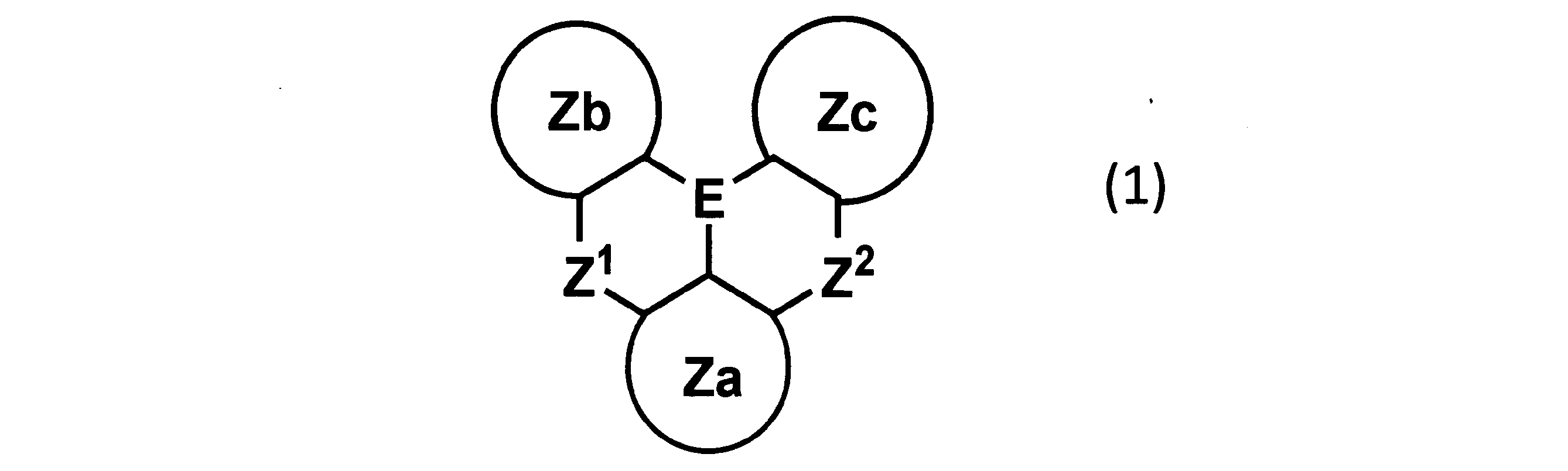
環Za、環Zbおよび環Zcは、それぞれ独立に、置換もしくは無置換の環形成炭素数6~30のアリール環、または置換もしくは無置換の環形成炭素数4~30のヘテロアリール環である。Z1およびZ2は、それぞれ独立に、酸素原子、NRa(置換基Raを有する窒素原子)または硫黄原子である。Z1がNRaである場合、Raは環Zaもしくは環Zbと結合して環を形成してもよい。Z2がNRaである場合、Raは環Zaもしくは環Zcと結合して環を形成してもよい。Eは、ホウ素原子、リン原子、SiRb(置換基Rbを有するケイ素原子)またはP=Oである。
Raは、それぞれ独立に、水素、置換もしくは無置換のアルキル基、置換もしくは無置換のシクロアルキル基、置換もしくは無置換の複素環基、置換もしくは無置換のアルケニル基、置換もしくは無置換のシクロアルケニル基、置換もしくは無置換のアルキニル基、置換もしくは無置換のアリール基、置換もしくは無置換のヘテロアリール基、水酸基、チオール基、置換もしくは無置換のアルコキシ基、置換もしくは無置換のアルキルチオ基、置換もしくは無置換のアリールエーテル基、置換もしくは無置換のアリールチオエーテル基、ハロゲン、シアノ基、アルデヒド基、置換もしくは無置換のカルボニル基、置換もしくは無置換のカルボキシル基、置換もしくは無置換のオキシカルボニル基、置換もしくは無置換のエステル基、置換もしくは無置換のカルバモイル基、置換もしくは無置換のアミド基、スルホニル基、置換もしくは無置換のスルホン酸エステル基、置換もしくは無置換のスルホンアミド基、置換もしくは無置換のアミノ基、ニトロ基、置換もしくは無置換のシリル基、置換もしくは無置換のシロキサニル基、置換もしくは無置換のボリル基、置換もしくは無置換のホスフィンオキシド基、置換もしくは無置換のイミノ基、および隣接置換基との間に形成される縮合環および脂肪族環の中から選ばれる。また、Raは、前記置換基でさらに置換されていてもよい。RbはRaと同義である。
[2]Eがホウ素原子であり、かつZ1およびZ2がそれぞれ独立に酸素原子またはNRaである、[1]に記載の光センサ。
[3]環Za、環Zbおよび環Zcが、それぞれ独立に、置換もしくは無置換の環形成炭素数6~30のアリール環である、[1]または[2]に記載の光センサ。
[4]Raが置換もしくは無置換のアリール基である、[1]~[3]のいずれかに記載の光センサ。
[5]前記光電変換層が、前記一般式(1)で表される構造を有する化合物として下記一般式(3)または(4)で表される構造を有する化合物を含む、[1]~[4]のいずれかに記載の光センサ。

(一般式(3)または(4)におけるEは、一般式(1)におけるEと同義である。一般式(3)または(4)における環Za~環Zeは、一般式(1)における環Za、環Zbおよび環Zcと同義である。環Zbと環Zdおよび環Zcと環Zeは隣接置換基との間で環構造を形成してもよい。)
[6]前記光電変換層が、一般式(1)で表される構造を有する多量体を含む、[1]~[5]のいずれかに記載の光センサ。
[7]前記一般式(1)で表される構造を有する多量体が下記一般式(5)、(6)または(7)で表される構造を有する化合物である、[6]に記載の光センサ。
[6]前記光電変換層が、一般式(1)で表される構造を有する多量体を含む、[1]~[5]のいずれかに記載の光センサ。
[7]前記一般式(1)で表される構造を有する多量体が下記一般式(5)、(6)または(7)で表される構造を有する化合物である、[6]に記載の光センサ。
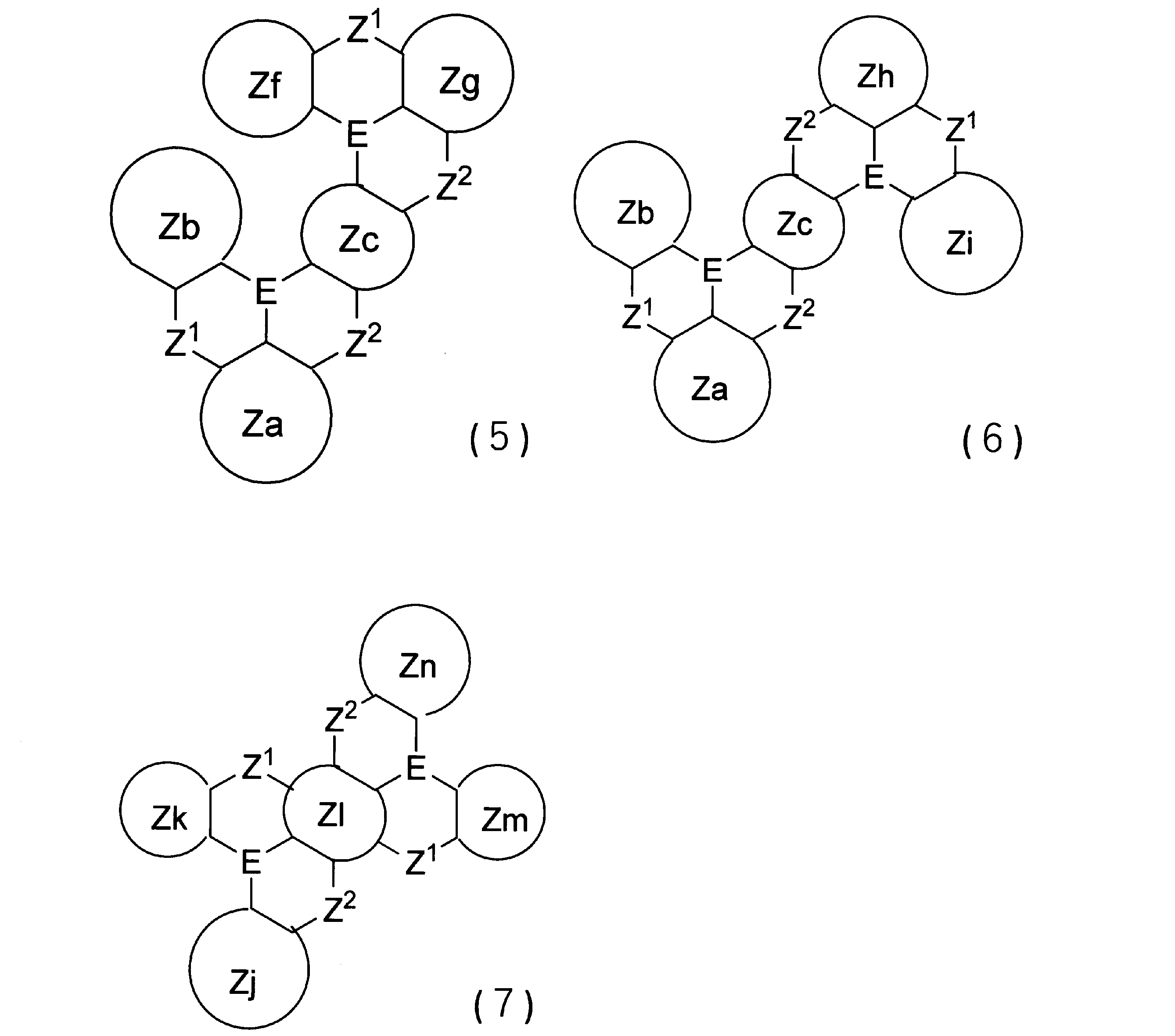
(一般式(5)、(6)または(7)におけるE、Z1およびZ2は、一般式(1)におけるE、Z1およびZ2と同義である。一般式(5)、(6)または(7)における環Za~環Zcおよび環Zf~環Znは、一般式(1)における環Za、環Zbおよび環Zcと同義である。)
[8]前記光電変換層がさらにn型有機半導体を含有する、[1]~[7]のいずれかに記載の光センサ。
[9]前記光電変換層と前記陽極の間に正孔取り出し層を有し、前記正孔取り出し層がハロゲン原子および/またはシアノ基を含有する化合物を含む、[1]~[8]のいずれかに記載の光センサ。
[10]前記ハロゲン原子および/またはシアノ基を含有する化合物が下記一般式(2)で表される化合物である、[9]に記載の光センサ。
[8]前記光電変換層がさらにn型有機半導体を含有する、[1]~[7]のいずれかに記載の光センサ。
[9]前記光電変換層と前記陽極の間に正孔取り出し層を有し、前記正孔取り出し層がハロゲン原子および/またはシアノ基を含有する化合物を含む、[1]~[8]のいずれかに記載の光センサ。
[10]前記ハロゲン原子および/またはシアノ基を含有する化合物が下記一般式(2)で表される化合物である、[9]に記載の光センサ。

上記一般式(2)中、R1~R6はそれぞれ同一でも異なっていても良く、置換もしくは無置換のアリール基、置換もしくは無置換のヘテロアリール基、シアノ基、ニトロ基、ハロゲン原子およびハロゲン化アルキル基からなる群より選ばれる。ただし、R1~R6のうち少なくとも1つはシアノ基またはハロゲン原子である。
[11][1]~[10]のいずれかに記載の光センサと有機発光素子とを有し、前記有機発光素子の光を利用して対象情報を検知する機能を有する、表示装置。
[12]前記対象情報が指紋情報である、[11]に記載の表示装置。
[13]前記対象情報が静脈情報である、[11]に記載の表示装置。
[11][1]~[10]のいずれかに記載の光センサと有機発光素子とを有し、前記有機発光素子の光を利用して対象情報を検知する機能を有する、表示装置。
[12]前記対象情報が指紋情報である、[11]に記載の表示装置。
[13]前記対象情報が静脈情報である、[11]に記載の表示装置。
本発明の光センサにより、青~赤色光の光検出において、波長選択性に優れ、高い光電変換効率を示す光センサを提供することができる。
以下、本発明の実施の形態を具体的に説明するが、本発明は以下の実施の形態に限定されるものではなく、目的や用途に応じて種々に変更して実施することができる。
本発明の光センサは、陽極と陰極の間に光電変換層が存在し、光を電気信号に変換する光センサであって、光電変換層が、下記一般式(1)で表される構造を有する化合物、または下記一般式(1)で表される構造を有する多量体を含む、光センサである。

環Za、環Zbおよび環Zcは、それぞれ独立に、置換もしくは無置換の環形成炭素数6~30のアリール環、または置換もしくは無置換の環形成炭素数4~30のヘテロアリール環である。Z1およびZ2は、それぞれ独立に、酸素原子、NRa(置換基Raを有する窒素原子)または硫黄原子である。Z1がNRaである場合、Raは環Zaもしくは環Zbと結合して環を形成してもよい。Z2がNRaである場合、Raは環Zaもしくは環Zcと結合して環を形成してもよい。Eは、ホウ素原子、リン原子、SiRb(置換基Rbを有するケイ素原子)またはP=Oである。
Raは、それぞれ独立に、水素原子、置換もしくは無置換のアルキル基、置換もしくは無置換のシクロアルキル基、置換もしくは無置換の複素環基、置換もしくは無置換のアルケニル基、置換もしくは無置換のシクロアルケニル基、置換もしくは無置換のアルキニル基、置換もしくは無置換のアリール基、置換もしくは無置換のヘテロアリール基、水酸基、チオール基、置換もしくは無置換のアルコキシ基、置換もしくは無置換のアルキルチオ基、置換もしくは無置換のアリールエーテル基、置換もしくは無置換のアリールチオエーテル基、ハロゲン、シアノ基、アルデヒド基、置換もしくは無置換のカルボニル基、置換もしくは無置換のカルボキシル基、置換もしくは無置換のオキシカルボニル基、置換もしくは無置換のエステル基、置換もしくは無置換のカルバモイル基、置換もしくは無置換のアミド基、スルホニル基、置換もしくは無置換のスルホン酸エステル基、置換もしくは無置換のスルホンアミド基、置換もしくは無置換のアミノ基、ニトロ基、置換もしくは無置換のシリル基、置換もしくは無置換のシロキサニル基、置換もしくは無置換のボリル基、置換もしくは無置換のホスフィンオキシド基、置換もしくは無置換のイミノ基、および隣接置換基との間に形成される縮合環および脂肪族環の中から選ばれる。また、Raは、前記置換基でさらに置換されていてもよい。RbはRaと同義である。
本明細書の以下の説明の全てにおいて、化合物の分子内に存在する水素原子の同位体種は特に限定されず、例えば、分子内の水素原子がすべて1Hであってもよいし、一部または全部が2H(デューテリウムD)であってもよい。
本明細書の以下の説明の全てにおいて、「置換もしくは無置換の」という場合における「無置換」とは、水素原子または重水素原子が結合したことを意味する。以下に説明する化合物またはその部分構造において、「置換もしくは無置換の」という場合についても、上記と同様である。
また、上記の全ての基において、置換される場合の置換基としては、アルキル基、シクロアルキル基、複素環基、アルケニル基、シクロアルケニル基、アルキニル基、アリール基、ヘテロアリール基、水酸基、チオール基、アルコキシ基、アルキルチオ基、アリールエーテル基、アリールチオエーテル基、ハロゲン、シアノ基、アルデヒド基、カルボニル基、カルボキシル基、オキシカルボニル基、アミド基、スルホニル基、スルホン酸エステル基、スルホンアミド基、アミノ基、ニトロ基、シリル基、シロキサニル基、ボリル基、またはホスフィンオキシド基である。また、これらの置換基は、さらに上述の置換基によって置換されていてもよい。
以下に記載するハロゲンおよび各基の説明は、本明細書の以下の説明の全てにおいて共通する。
アルキル基とは、例えば、メチル基、エチル基、n-プロピル基、イソプロピル基、n-ブチル基、sec-ブチル基、tert-ブチル基などの飽和脂肪族炭化水素基を示し、これは置換基を有していても有していなくてもよい。置換基としては、例えば、アルコキシ基、アルコキシカルボニル基、ハロゲン、アリール基、ヘテロアリール基等を挙げることができる。また、アルキル基の炭素数は、原料入手の容易性や蒸着安定性の観点から、1以上20以下が好ましく、1以上10以下がより好ましく、1以上6以下がさらに好ましい。ここで、アルキル基の炭素数には、置換基の炭素数は含めないこととし、この点は、以下の記載にも共通する。
シクロアルキル基とは、例えば、シクロプロピル基、シクロペンチル基、シクロヘキシル基、ノルボルニル基、アダマンチル基などの飽和脂環式炭化水素基を示し、これは置換基を有していても有していなくてもよい。置換基としては、アルキル基の置換基として例示した基が挙げられる。シクロアルキル基の環形成炭素数は、好ましくは、3以上20以下の範囲である。
複素環基とは、例えば、ピラン環、ピペリジン環、環状アミドなどの炭素以外の原子を環内に有する脂肪族環を示し、これは置換基を有していても有していなくてもよい。環形成原子数は特に限定されないが、好ましくは、3以上20以下の範囲である。
アルケニル基とは、例えば、ビニル基、アリル基、ブタジエニル基などの二重結合を含む不飽和脂肪族炭化水素基を示し、これは置換基を有していても有していなくてもよい。アルケニル基の炭素数は特に限定されないが、好ましくは、2以上20以下の範囲である。
シクロアルケニル基とは、例えば、シクロペンテニル基、シクロペンタジエニル基、シクロヘキセニル基などの二重結合を含む不飽和脂環式炭化水素基を示し、これは置換基を有していても有していなくてもよい。環形成炭素数は特に限定されないが、好ましくは、3以上20以下の範囲である。
アルキニル基とは、例えば、エチニル基などの三重結合を含む不飽和脂肪族炭化水素基を示し、これは置換基を有していても有していなくてもよい。アルキニル基の炭素数は特に限定されないが、好ましくは、2以上20以下の範囲である。
アリール基とは、例えば、フェニル基、ビフェニル基、ターフェニル基、ナフチル基、フルオレニル基、ベンゾフルオレニル基、ジベンゾフルオレニル基、フェナントリル基、アントラセニル基、ベンゾフェナントリル基、ベンゾアントラセニル基、クリセニル基、ピレニル基、フルオランテニル基、トリフェニレニル基、ベンゾフルオランテニル基、ジベンゾアントラセニル基、ペリレニル基、ヘリセニル基などの芳香族炭化水素基を示す。これは置換基を有していても有していなくてもよい。これらの中でも、フェニル基、ビフェニル基、ターフェニル基、ナフチル基、フルオレニル基、フェナントリル基、アントラセニル基、ピレニル基、フルオランテニル基、トリフェニレニル基が好ましい。環形成炭素数は特に限定されないが、好ましくは、6以上40以下、より好ましくは、6以上30以下の範囲である。また、置換のアリール基においては、そのアリール基中の隣接する2つの炭素原子上に各々置換基がある場合、それらの置換基同士で環構造を形成していてもよい。その結果としてできた基は、その構造に応じて、「置換のアリール基」、「2つ以上の環が縮環した構造を有するアリール基」、「2つ以上の環が縮環した構造を有するヘテロアリール基」のいずれか1つ以上に該当しうる。
ヘテロアリール基とは、例えば、ピリジル基、フラニル基、チオフェニル基、キノリニル基、イソキノリニル基、ピラジニル基、ピリミジル基、ピリダジニル基、トリアジニル基、ナフチリジニル基、シンノリニル基、フタラジニル基、キノキサリニル基、キナゾリニル基、ベンゾフラニル基、ベンゾチオフェニル基、インドリル基、ジベンゾフラニル基、ジベンゾチオフェニル基、カルバゾリル基、ベンゾカルバゾリル基、カルボリニル基、インドロカルバゾリル基、ベンゾフロカルバゾリル基、ベンゾチエノカルバゾリル基、ジヒドロインデノカルバゾリル基、ベンゾキノリニル基、アクリジニル基、ジベンゾアクリジニル基、ベンゾイミダゾリル基、イミダゾピリジル基、ベンゾオキサゾリル基、ベンゾチアゾリル基、フェナントロリニル基などの、炭素以外の原子を一個または複数個環内に有する環状芳香族基を示す。ただし、ナフチリジニル基とは、1,5-ナフチリジニル基、1,6-ナフチリジニル基、1,7-ナフチリジニル基、1,8-ナフチリジニル基、2,6-ナフチリジニル基、2,7-ナフチリジニル基のいずれかを示す。ヘテロアリール基は置換基を有していても有していなくてもよい。環形成原子数は特に限定されないが、好ましくは、3以上40以下、より好ましくは、3以上30以下の範囲である。
アルコキシ基とは、例えば、メトキシ基、エトキシ基、プロポキシ基などのエーテル結合を介して脂肪族炭化水素基が結合した官能基を示し、この脂肪族炭化水素基は置換基を有していても有していなくてもよい。置換基としては、アルキル基の置換基として例示した基が挙げられる。アルコキシ基の炭素数は、好ましくは、1以上20以下の範囲である。
アルキルチオ基とは、アルコキシ基のエーテル結合の酸素原子が硫黄原子に置換されたものである。アルキルチオ基の炭化水素基は、置換基を有していても有していなくてもよい。アルキルチオ基の炭素数は、特に限定されないが、好ましくは、1以上20以下の範囲である。
アリールエーテル基とは、例えば、フェノキシ基等、エーテル結合を介した芳香族炭化水素基が結合した官能基を示し、芳香族炭化水素基は、置換基を有していても有していなくてもよい。アリールエーテル基の炭素数は、特に限定されないが、好ましくは、6以上40以下の範囲である。
アリールチオエーテル基とは、アリールエーテル基のエーテル結合の酸素原子が硫黄原子に置換されたものである。アリールチオエーテル基における芳香族炭化水素基は、置換基を有していても有していなくてもよい。アリールチオエーテル基の炭素数は、特に限定されないが、好ましくは、6以上40以下の範囲である。
ハロゲンとは、フッ素、塩素、臭素およびヨウ素から選ばれる原子を示す。また、カルボニル基、カルボキシル基、オキシカルボニル基、カルバモイル基は、置換基を有していても有していなくてもよい。ここで、置換基としては、例えば、アルキル基、シクロアルキル基、アリール基、ヘテロアリール基等が挙げられ、これら置換基は、さらに置換されてもよい。
アミノ基とは、置換もしくは無置換のアミノ基である。置換する場合の置換基としては、例えば、アリール基、ヘテロアリール基、直鎖アルキル基、分岐アルキル基が挙げられる。アリール基、ヘテロアリール基としては、フェニル基、ナフチル基、ピリジル基、キノリニル基が好ましい。これら置換基は、さらに置換されてもよい。炭素数は、特に限定されないが、好ましくは、2以上50以下、より好ましくは6以上40以下、特に好ましくは6以上30以下の範囲である。
シリル基とは、例えば、トリメチルシリル基、トリエチルシリル基、tert-ブチルジメチルシリル基、プロピルジメチルシリル基、ビニルジメチルシリル基等のアルキルシリル基や、フェニルジメチルシリル基、tert-ブチルジフェニルシリル基、トリフェニルシリル基、トリナフチルシリル基等のアリールシリル基を示す。ケイ素上の置換基は、さらに置換されてもよい。シリル基の炭素数は、特に限定されないが、好ましくは、1以上30以下の範囲である。
シロキサニル基とは、例えば、トリメチルシロキサニル基等のエーテル結合を介したケイ素化合物基を示す。ケイ素上の置換基は、さらに置換されてもよい。また、ボリル基とは、置換もしくは無置換のボリル基である。置換する場合の置換基としては、例えば、アリール基、ヘテロアリール基、直鎖アルキル基、分岐アルキル基、アリールエーテル基、アルコキシ基、ヒドロキシル基が挙げられる。中でも、アリール基、アリールエーテル基が好ましい。
ホスフィンオキシド基とは、-P(=O)R10R11で表される基である。ホスフィンオキシド基のR10R11は、上述の置換する場合の置換基と同様の群から選ばれる。
光センサの光電変換効率を向上させるためには、光電変換層に用いられる材料の特性として、主に、(i)検出波長領域の光を効率よく吸収し励起状態を形成すること、および(ii)励起状態形成後に速やかに電荷分離し、印加電圧に沿って電荷をロスなく電極方向へ輸送すること、の2点が求められる。一般式(1)で表される構造を有する化合物、および一般式(1)で表される構造を有する多量体は、平面性の高い骨格を有している。これらの材料を光電変換層として用いた場合、隣接する分子間でそれぞれの分子軌道の重なりが大きくなる。したがって電荷分離後の電荷をロスなく電極方向へ輸送することが可能となり、より大きな電流を取り出せ、光電変換効率の向上が期待できる。
通常、有機薄膜太陽電池における光電変換層には紫外領域から赤外領域の幅広い波長領域の光を吸収することが求められるが、光センサにおける光電変換層には、検出光の波長領域に応じた特定の波長領域に強い吸収を有することが求められる。光センサの検出光として、LEDや有機電界発光素子といった既存の光源からの放射光を利用する場合、紫外領域、青色領域、緑色領域、または赤色領域に強い吸収ピークを有する材料を光電変換層に用いることが好ましく、青色領域、緑色領域または赤色領域に強い吸収ピークを有する材料を用いることがより好ましい。一般式(1)で表される構造を有する化合物、および一般式(1)で表される構造を有する多量体は、E、Z1、Z2、および/または置換基の種類や環構造により、吸収ピークを紫外領域、青色領域、緑色領域または赤色領域にチューニングすることが可能である。すなわち、一般式(1)で表される構造を有する化合物、および一般式(1)で表される構造を有する多量体により、紫外光、青色光、緑色光または赤色光に高感度であり、検出光の波長選択性に優れた光センサを得ることができる。
本発明の光センサによる検出光の発光スペクトルは、波長330~400nmの紫外領域、波長420~470nmの青色領域、または波長480~560nmの緑色領域、580~700nmの赤色領域にピークを有することが好ましく、波長420~470nmの青色領域、波長480~560nmの緑色領域または580~700nmの赤色領域にピークを有することがより好ましい。
Eは、ホウ素原子、リン原子またはP=Oであることがより好ましく、ホウ素原子であることがさらに好ましい。Z1およびZ2は、それぞれ独立に、酸素原子、硫黄原子またはNRaであることがより好ましく、NRaであることがさらに好ましい。青色領域または緑色領域に強い吸収ピークを有するという観点では、Eがホウ素原子であり、かつZ1およびZ2がそれぞれ独立に酸素原子またはNRaであることが好ましい。
環Za、環Zbおよび環Zcにおける置換もしくは無置換の環形成炭素数6~30のアリール環としては、ベンゼン環、ナフタレン環、フェナントレン環、クリセン環、アントラセン環、ピレン環といった芳香族炭化水素環が挙げられる。これらの中でも、良好な昇華性を確保する観点から、ベンゼン環が好ましい。また、環形成炭素数4~30のヘテロアリール環としては、フラン環、チオフェン環、ピリジン環、キノリン環、フェナントロリン環といった芳香族ヘテロアリール環構造が挙げられる。これらの中でも、原料入手のしやすさや合成の難易度の観点から、ピリジン環が好ましい。
材料の化学的な安定性や、後述の良好な正孔輸送性を確保するという観点から、環Za、環Zbおよび環Zcは、それぞれ独立に、置換もしくは無置換の環形成炭素数6~30のアリール環であることが好ましく、良好な昇華性を確保するという観点で、アリール環の中でもベンゼン環であることがより好ましい。
環Za、環Zbまたは環Zcは置換基を有していても有していなくてもよく、置換基を有している場合はRaと同義の置換基を有していることが好ましい。より好ましい置換基としては、アミノ基、アルキル基、シクロアルキル基、アリール基およびヘテロアリール基であり、さらに好ましくは、アミノ基、アリール基およびヘテロアリール基であり、特に好ましくはアミノ基である。アミノ基の中でも、ジアリールアミノ基が特に好ましい。
一般式(1)で表される構造を有する化合物、および一般式(1)で表される構造を有する多量体を含む層は、光電変換層として機能するが、電荷分離後、印加電圧に沿って、主に正孔を電極方向に輸送するp型半導体層としても機能する。正孔をロスなく輸送するためには、適切なHOMO(Highest Occupied Molecular Orbital)軌道のエネルギー準位を有している必要があるが、そのためには、環Za、環Zbおよび環Zcが置換もしくは無置換の環形成炭素数6~30のアリール環であることが好ましい。
さらに良好な正孔輸送性を得るためには隣接分子間とのHOMO軌道の重なりを大きくする必要があるが、この観点で、Raが置換もしくは無置換のアリール基または置換もしくは無置換のヘテロアリール基であることが好ましく、さらに適切なHOMO軌道のエネルギー準位を有するという観点で、Raが置換もしくは無置換のアリール基であることがより好ましい。好ましい置換もしくは無置換のアリール基としては、フェニル基、ナフチル基、ビフェニル基、フルオレニル基、アントラセニル基、ピレニル基、フェナントレニル基、クリセニル基、トリフェニレニル基またはフルオランテニル基等があげられるが、フェニル基、ナフチル基、ビフェニル基、フルオレニル基またはフェナントレニル基がより好ましく、良好な昇華性を示すという観点でフェニル基、ナフチル基、ビフェニル基またはフルオレニル基がさらに好ましく、フェニル基が最も好ましい。
一般式(1)で表される構造を有する化合物は、下記一般式(3)または(4)で表される構造を有する化合物であることが好ましい。すなわち、前記光電変換層が、前記一般式(1)で表される構造を有する化合物として下記一般式(3)または(4)で表される構造を有する化合物を含むことが好ましい。
また、前記光電変換層が、前記一般式(1)で表される構造を有する化合物として下記(3)で表される構造を有する化合物を含むことがより好ましい。
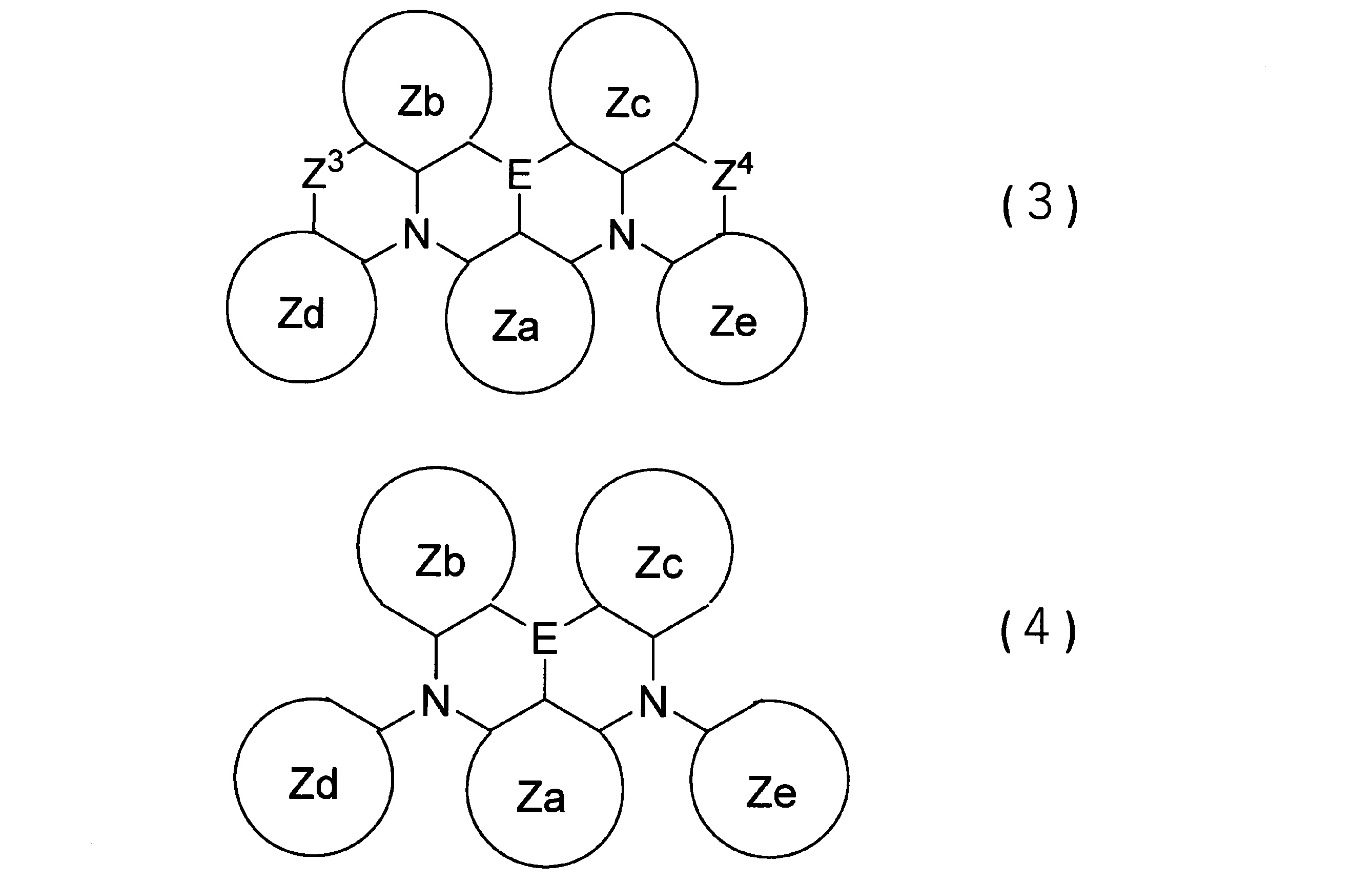
一般式(3)および(4)におけるE、Z3およびZ4は、一般式(1)におけるE、Z1およびZ2と同義である。一般式(3)および(4)における環Za~環Zeは、一般式(1)における環Za、環Zbおよび環Zcと同義である。環Zbと環Zdおよび環Zcと環Zeは隣接置換基との間で環構造を形成してもよい。
一般式(3)および(4)において、Eは一般式(1)の場合の説明と同様、ホウ素原子、リン原子またはP=Oであることがより好ましく、ホウ素原子であることがさらに好ましい。
Raは一般式(1)の説明と同様、置換もしくは無置換のアリール基または置換もしくは無置換のヘテロアリール基であることが好ましく、さらに適切なHOMO軌道のエネルギー準位を有するという観点で、Raが置換もしくは無置換のアリール基であることがより好ましい。好ましい置換もしくは無置換のアリール基としては、フェニル基、ナフチル基、ビフェニル基、フルオレニル基、アントラセニル基、ピレニル基、フェナントレニル基、クリセニル基、トリフェニレニル基またはフルオランテニル基等があげられるが、フェニル基、ナフチル基、ビフェニル基、フルオレニル基またはフェナントレニル基がより好ましく、良好な昇華性を示すという観点でフェニル基、ナフチル基、ビフェニル基またはフルオレニル基がさらに好ましく、フェニル基が最も好ましい。
一般式(3)および(4)において、環Za~環Zeは、一般式(1)の場合の説明と同様、無置換の環形成炭素数6~30のアリール環が好ましい。アリール環としてはベンゼン環、ナフタレン環、フェナントレン環、クリセン環、アントラセン環、ピレン環等が挙げられるが、平面性を確保した上でさらに良好な昇華性が得られるという観点で、ベンゼン環が好ましく、環Za~環Zeの全てがベンゼン環であることがより好ましい。
また、光電変換層が、一般式(1)で表される構造を有する多量体を含む場合、分子の平面性がさらに向上し、隣接分子間のHOMO軌道の重なりがより大きくなるため好ましい。
一般式(1)で表される構造を有する多量体としては、一般式(1)で表される構造が、単結合や、アルキレン基、アリーレン基、ヘテロアリーレン基、エーテル結合またはチオエーテル結合といった連結基を介して複数個結合した化合物や、下記一般式(5)、(6)または(7)で表される構造を有する化合物のように、複数の一般式(1)で表される構造が当該構造中の環Za~環Zcのいずれかを共有するような形の化合物が挙げられる。

一般式(5)、(6)または(7)におけるE、Z1およびZ2は、一般式(1)におけるE、Z1およびZ2と同義である。一般式(5)、(6)または(7)における環Za~環Zcおよび環Zf~環Znは、一般式(1)における環Za、環Zbおよび環Zcと同義である。
一般式(1)で表される構造を有する多量体が一般式(5)、(6)または(7)で表される構造を有する化合物である場合、分子がより剛直で平面性が高くなるため、正孔輸送性が向上し、光電変換効率向上に寄与できるので好ましい。
一般式(5)、(6)または(7)において、Eは一般式(1)の場合の説明と同様、ホウ素原子、リン原子またはP=Oであることがより好ましく、ホウ素原子であることがさらに好ましい。
一般式(5)、(6)または(7)において、Z1およびZ2は、一般式(1)の場合の説明と同様、酸素原子、硫黄原子またはNRaであることがより好ましく、酸素原子またはNRaであることがさらに好ましい。
Raは一般式(1)の説明と同様、置換もしくは無置換のアリール基または置換もしくは無置換のヘテロアリール基であることが好ましく、さらに適切なHOMO軌道のエネルギー準位を有するという観点で、Raが置換もしくは無置換のアリール基であることがより好ましい。好ましい置換もしくは無置換のアリール基としては、フェニル基、ナフチル基、ビフェニル基、フルオレニル基、アントラセニル基、ピレニル基、フェナントレニル基、クリセニル基、トリフェニレニル基またはフルオランテニル基等があげられるが、フェニル基、ナフチル基、ビフェニル基、フルオレニル基またはフェナントレニル基がより好ましく、良好な昇華性を示すという観点でフェニル基、ナフチル基、ビフェニル基またはフルオレニル基がさらに好ましく、フェニル基が最も好ましい。
青色領域、緑色領域または赤色領域の光を効率よく吸収するという観点では、一般式(5)、(6)または(7)におけるEがホウ素原子であり、かつZ1およびZ2がそれぞれ独立に酸素原子またはNRaであることが好ましい。
一般式(5)、(6)または(7)において、環Za~環Zcおよび環Zf~環Znは、一般式(1)の場合の説明と同様、無置換の環形成炭素数6~30のアリール環が好ましい。アリール環としてはベンゼン環、ナフタレン環、フェナントレン環、クリセン環、アントラセン環、ピレン環等が挙げられるが、平面性を確保した上でさらに良好な昇華性が得られるという観点で、ベンゼン環が好ましく、環Za、環Zbおよび環Zf~環Ziの全てがベンゼン環であることがより好ましい。
以下に一般式(1)、(3)および(4)で表される構造を有する化合物の例を示すが、これらに限定されるものではない。
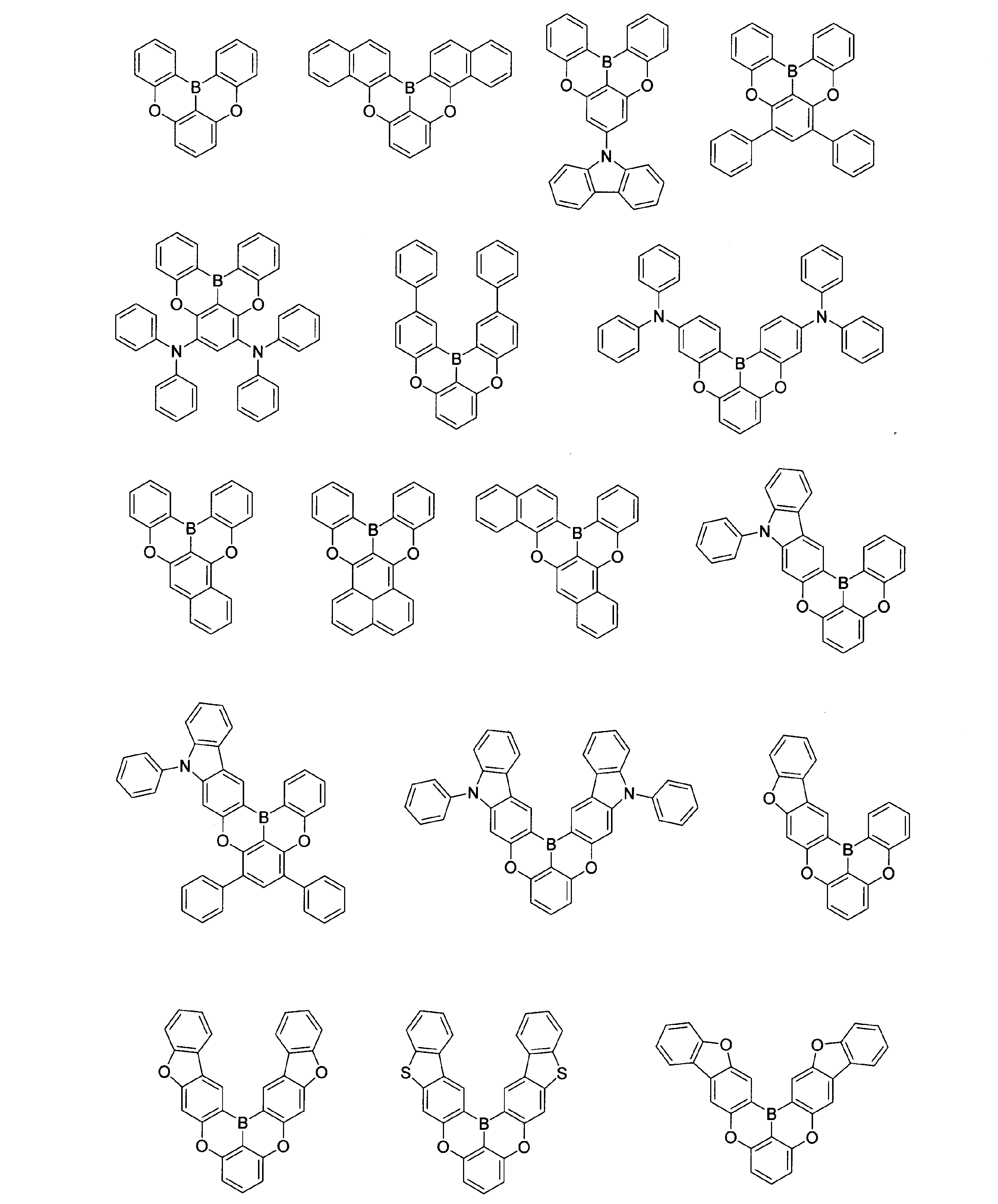
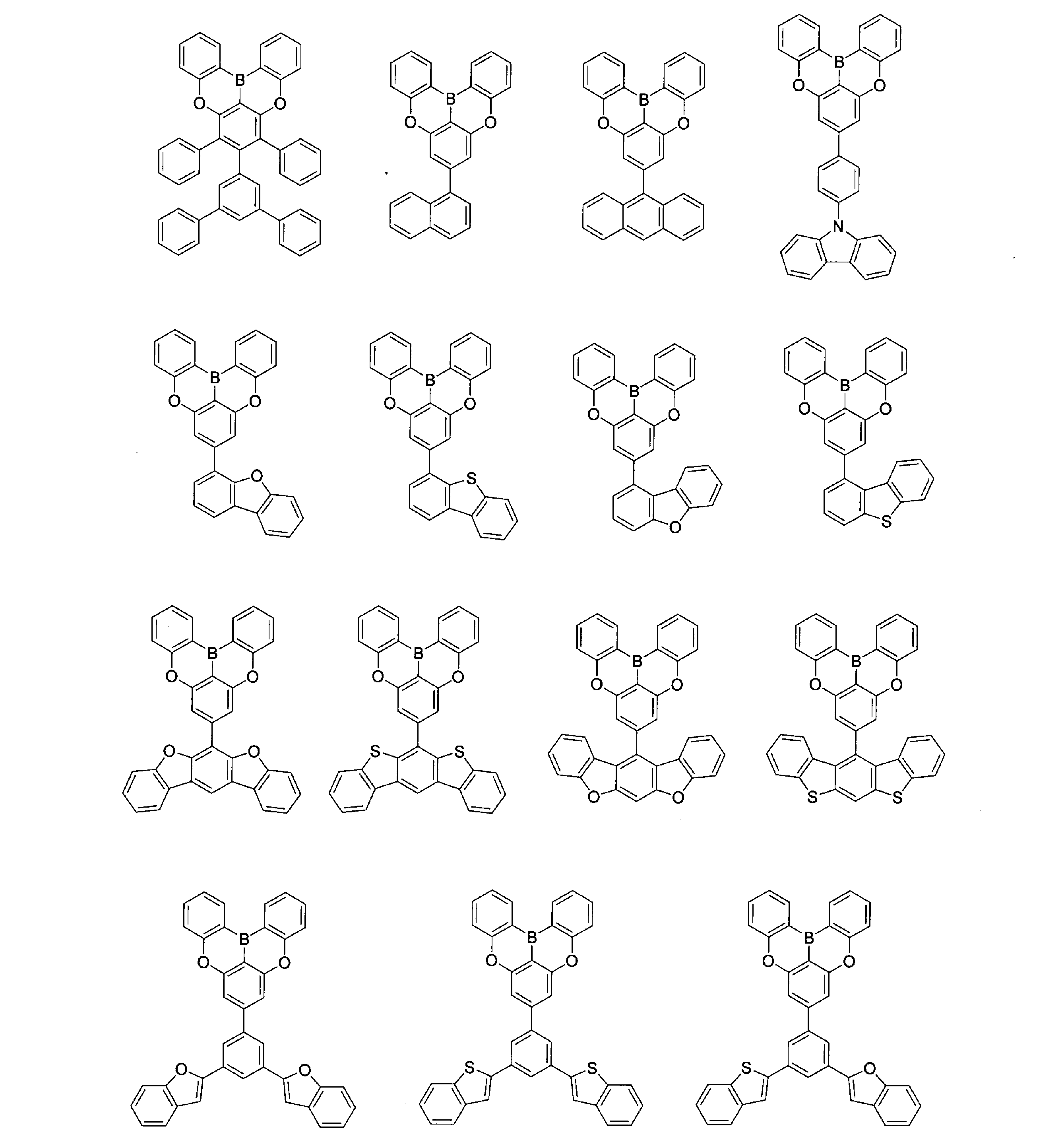
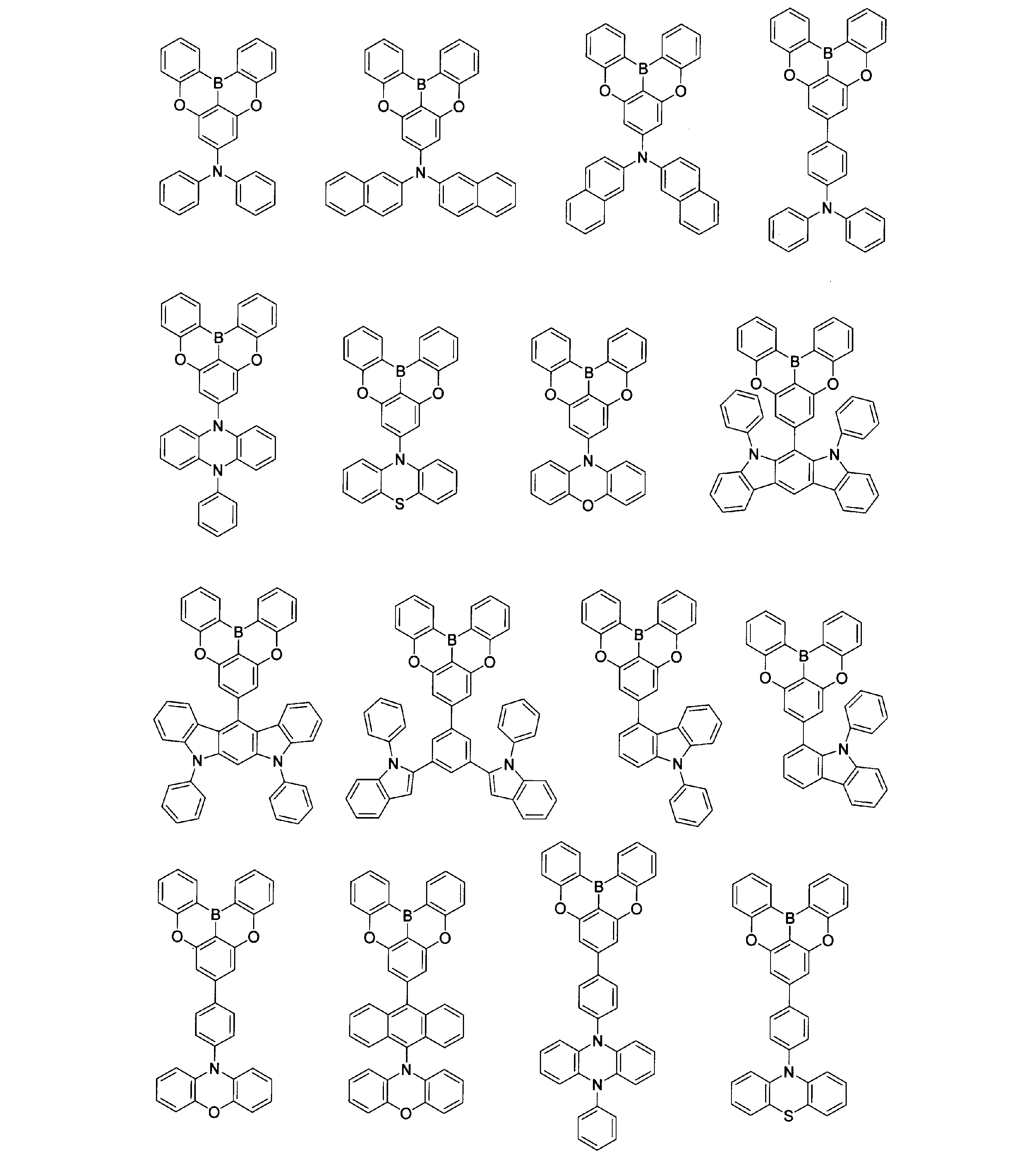

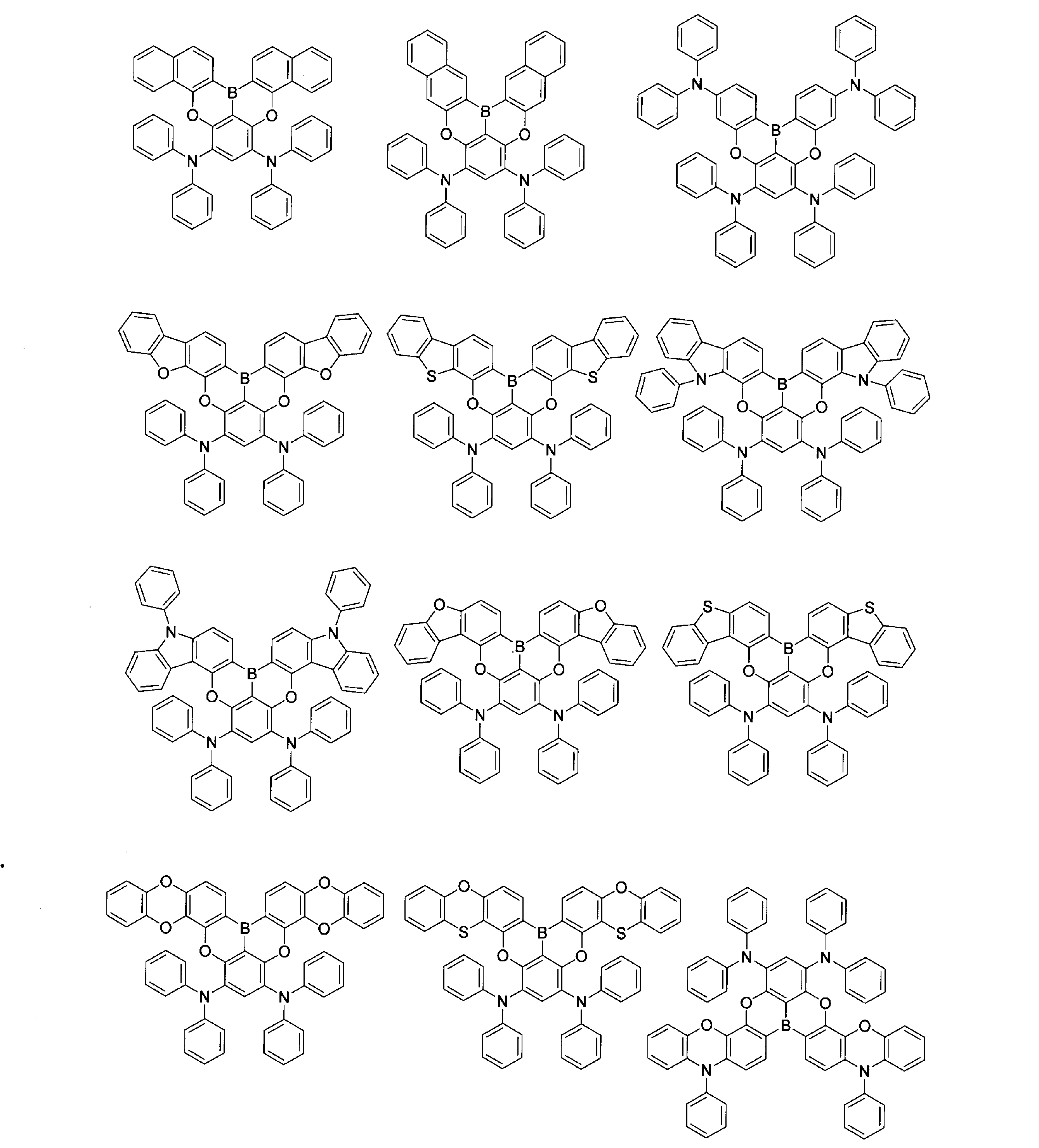
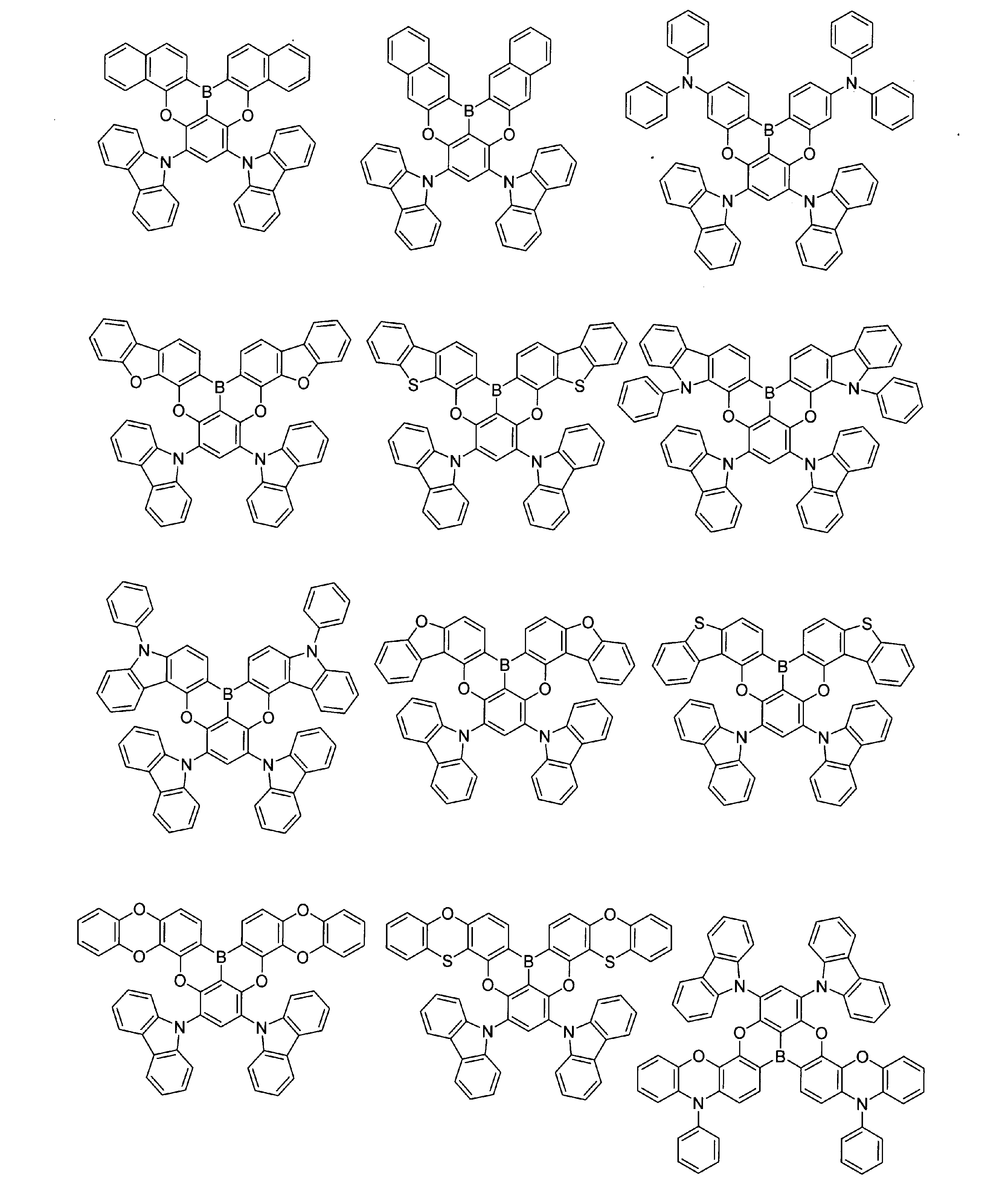
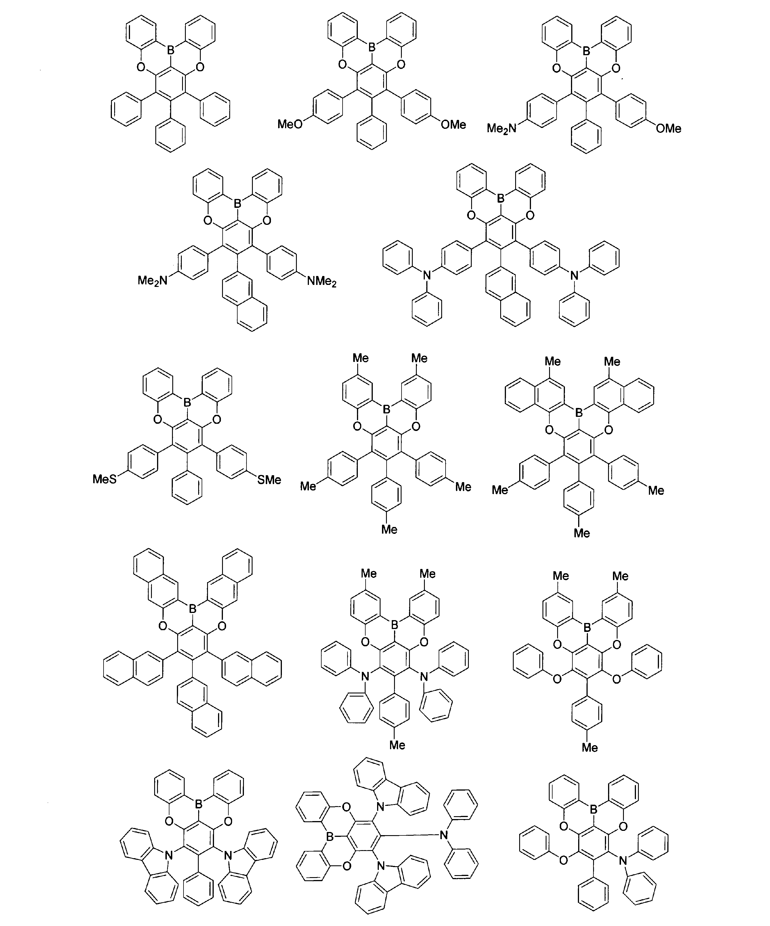
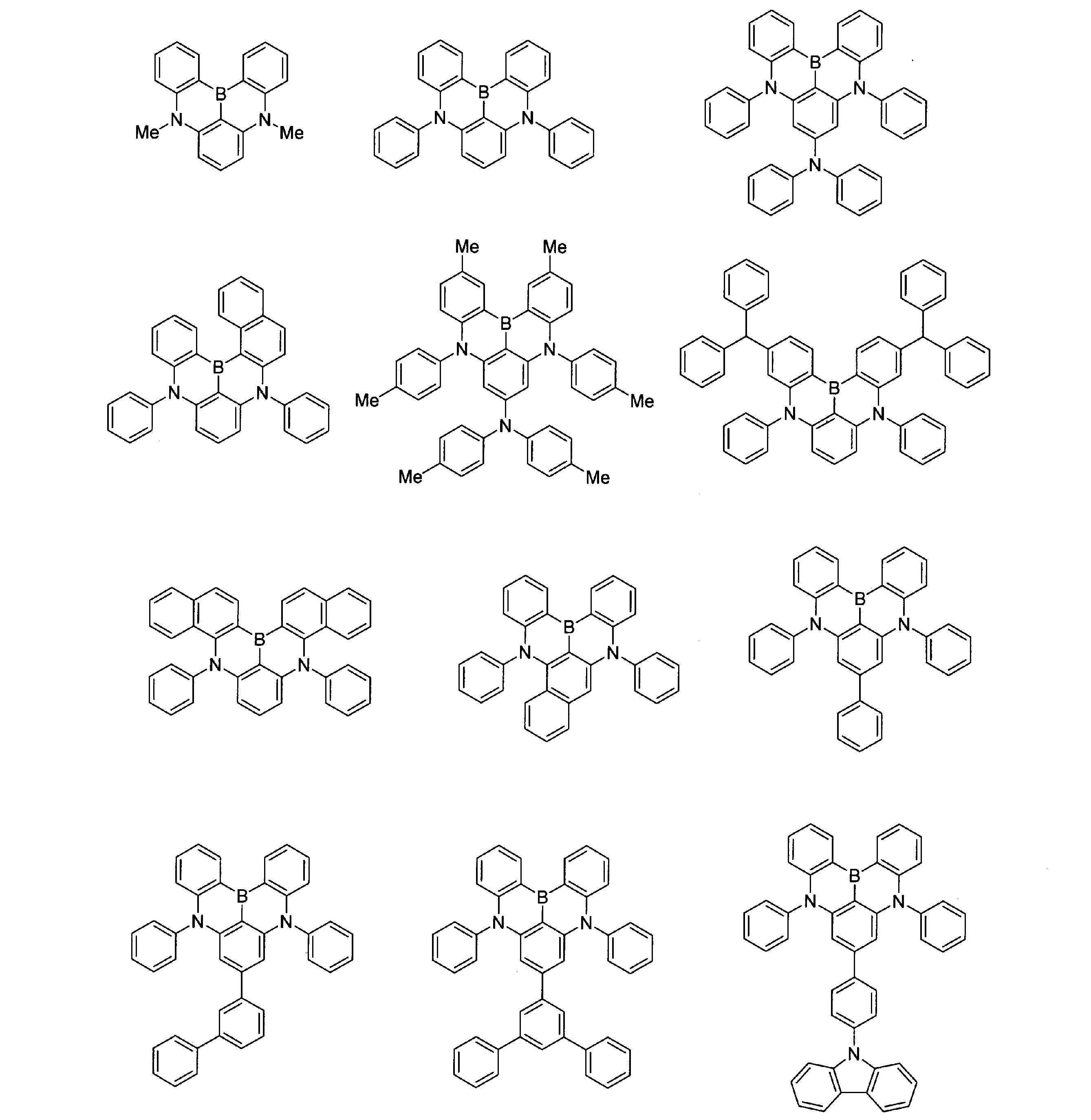

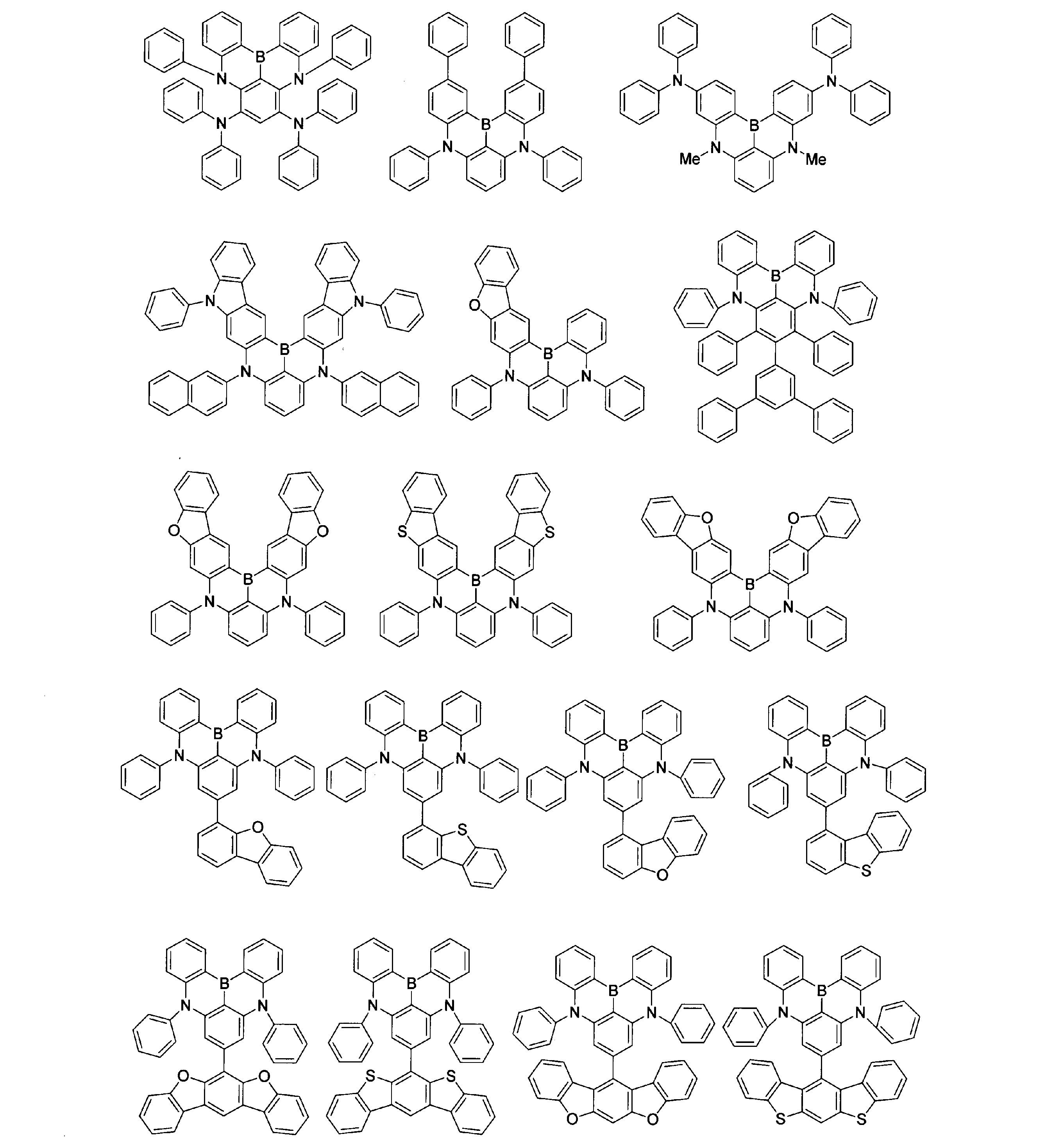

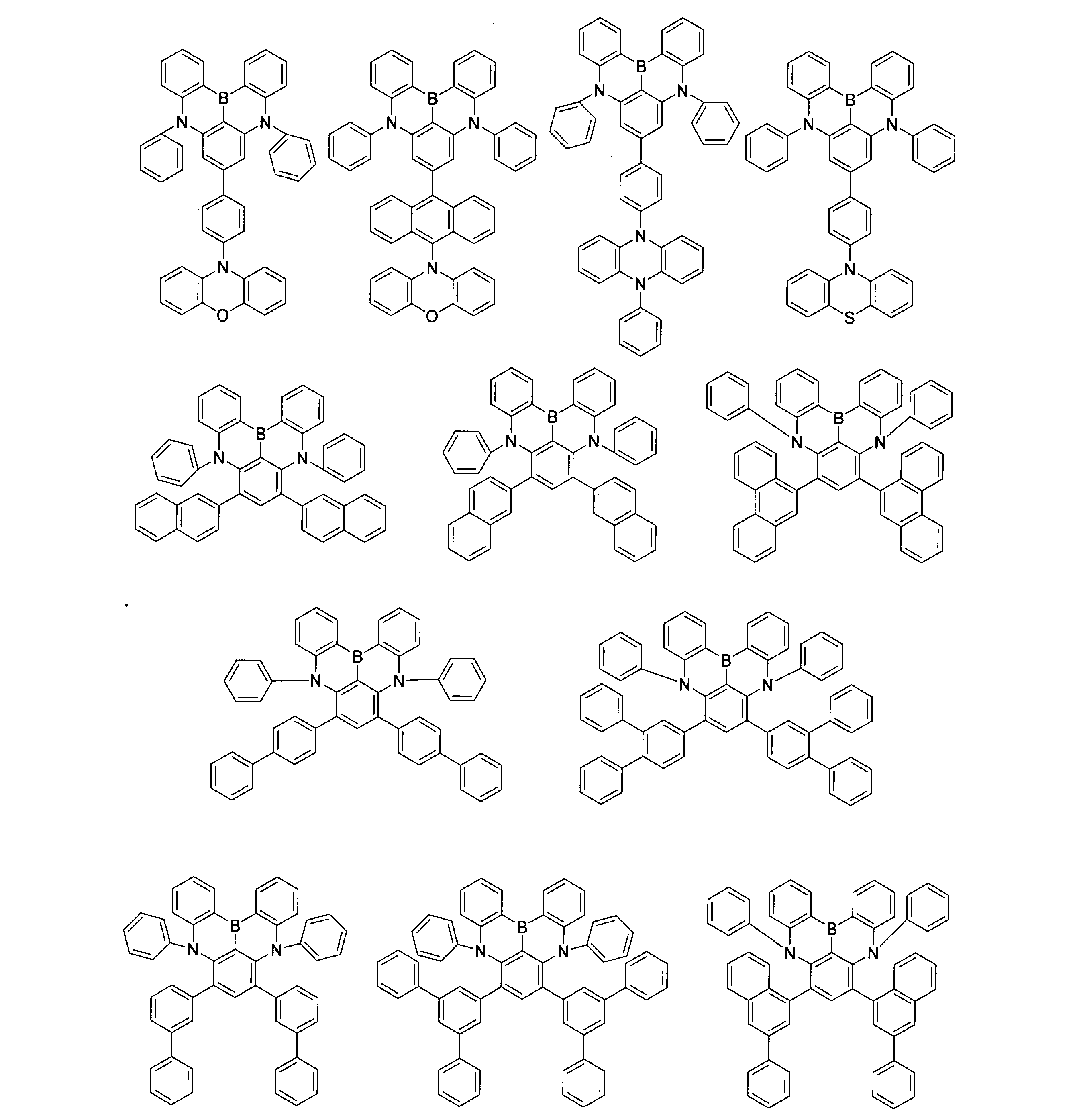
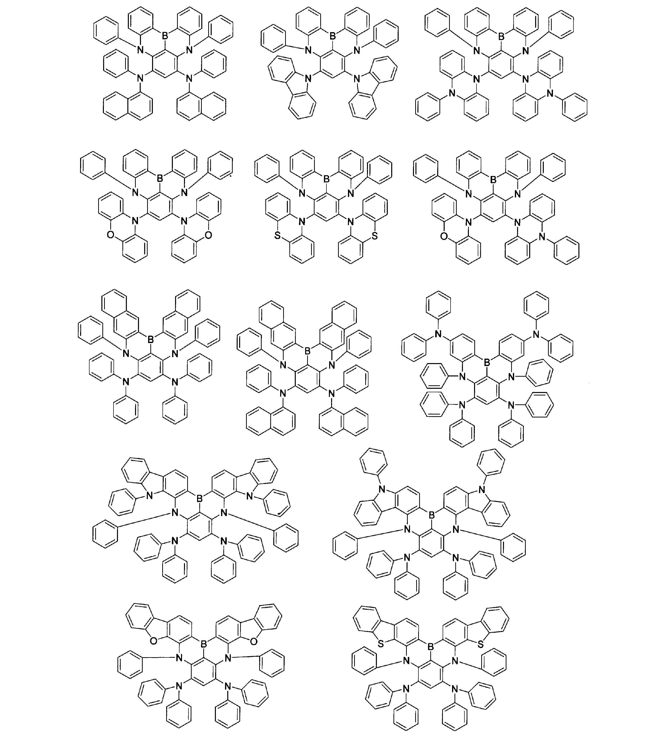

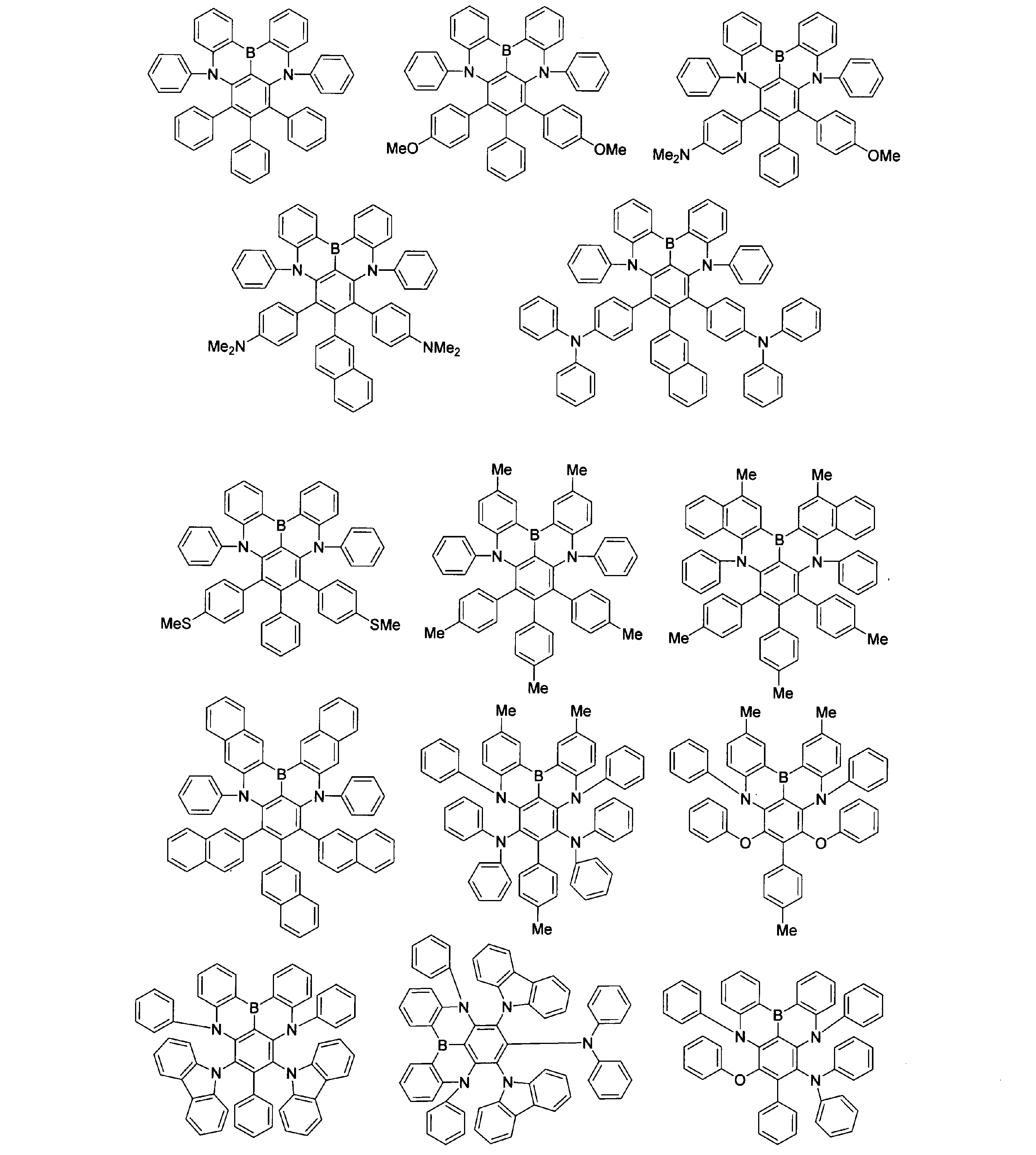
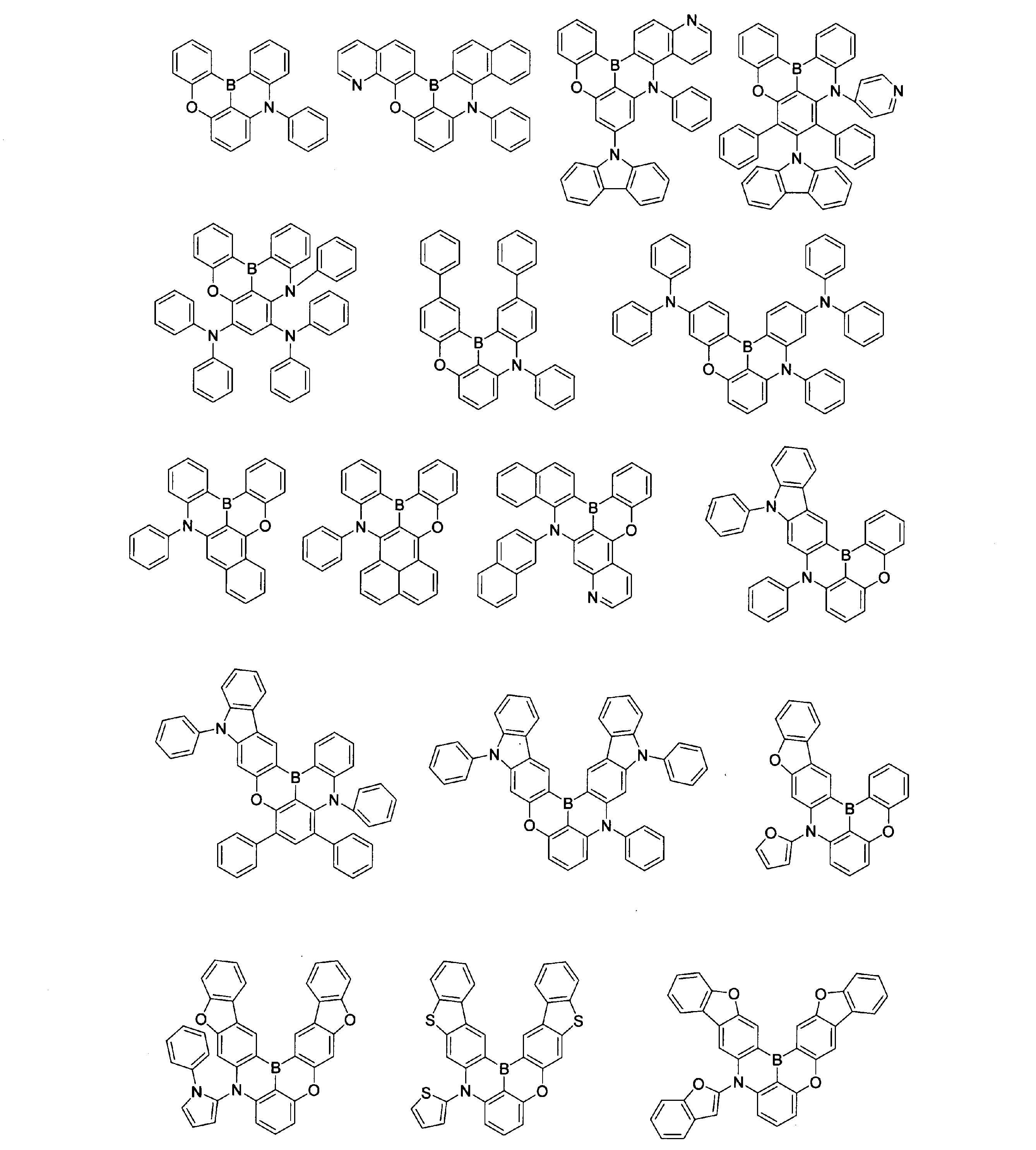
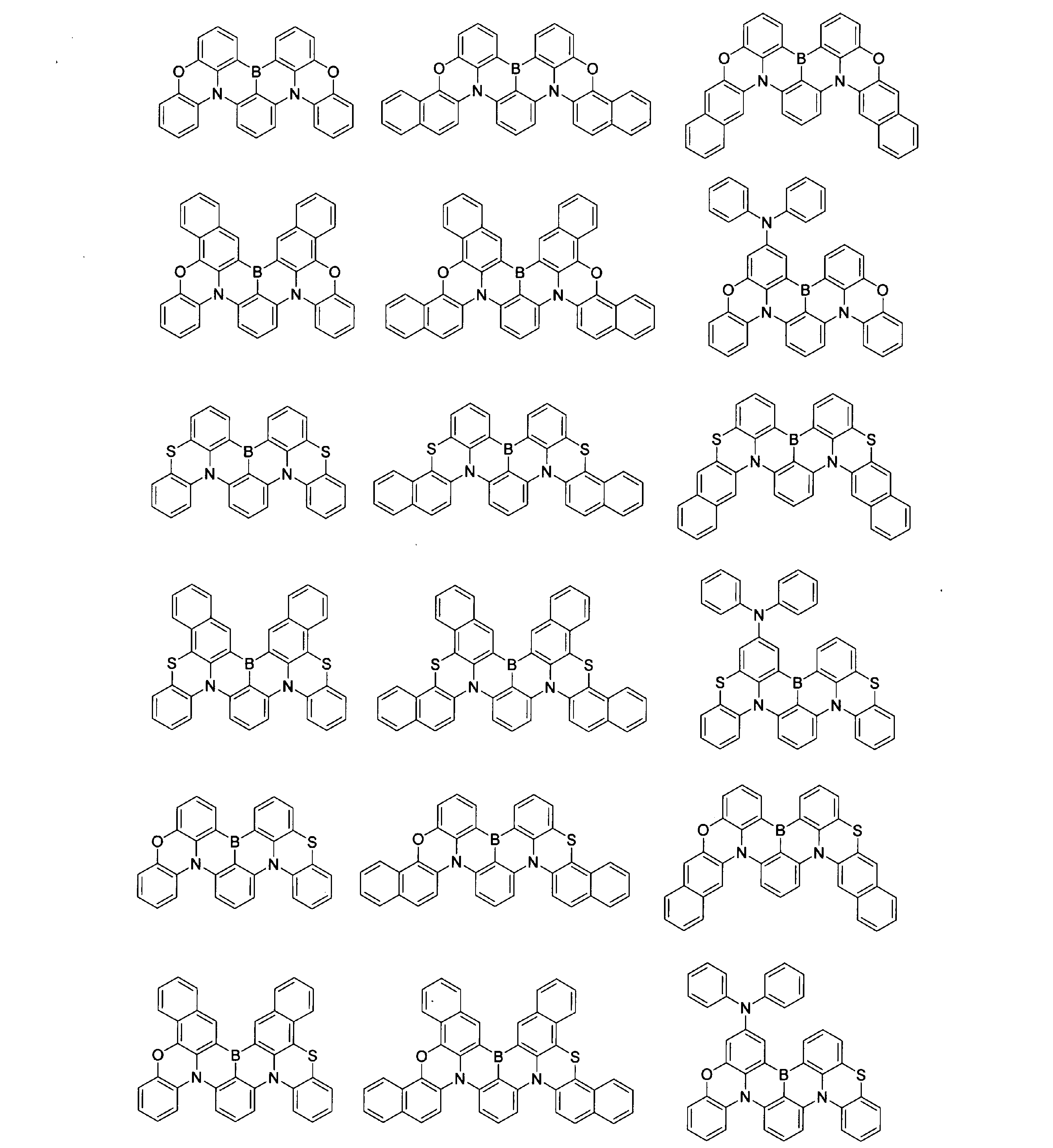
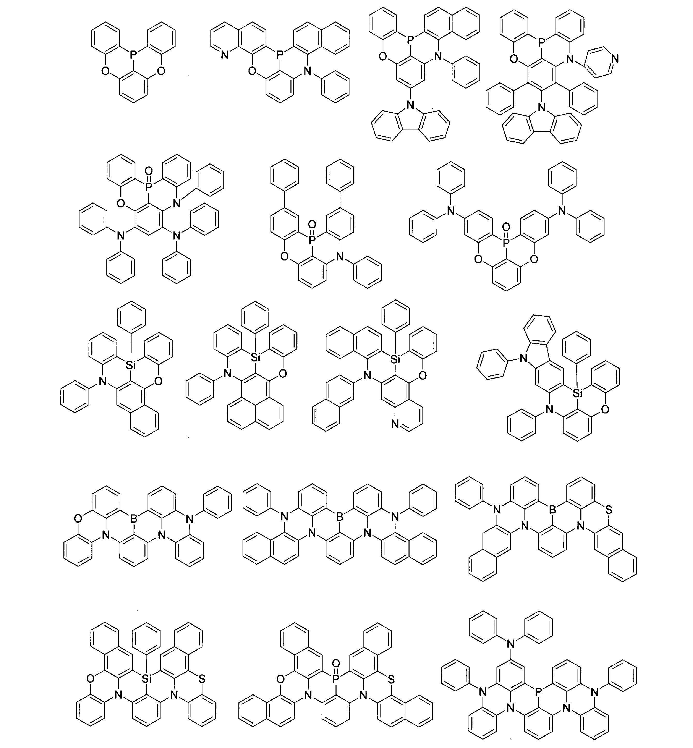
また以下に、一般式(5)、(6)または(7)で表される多量体化合物の例を示すが、これらに限定されるものではない。
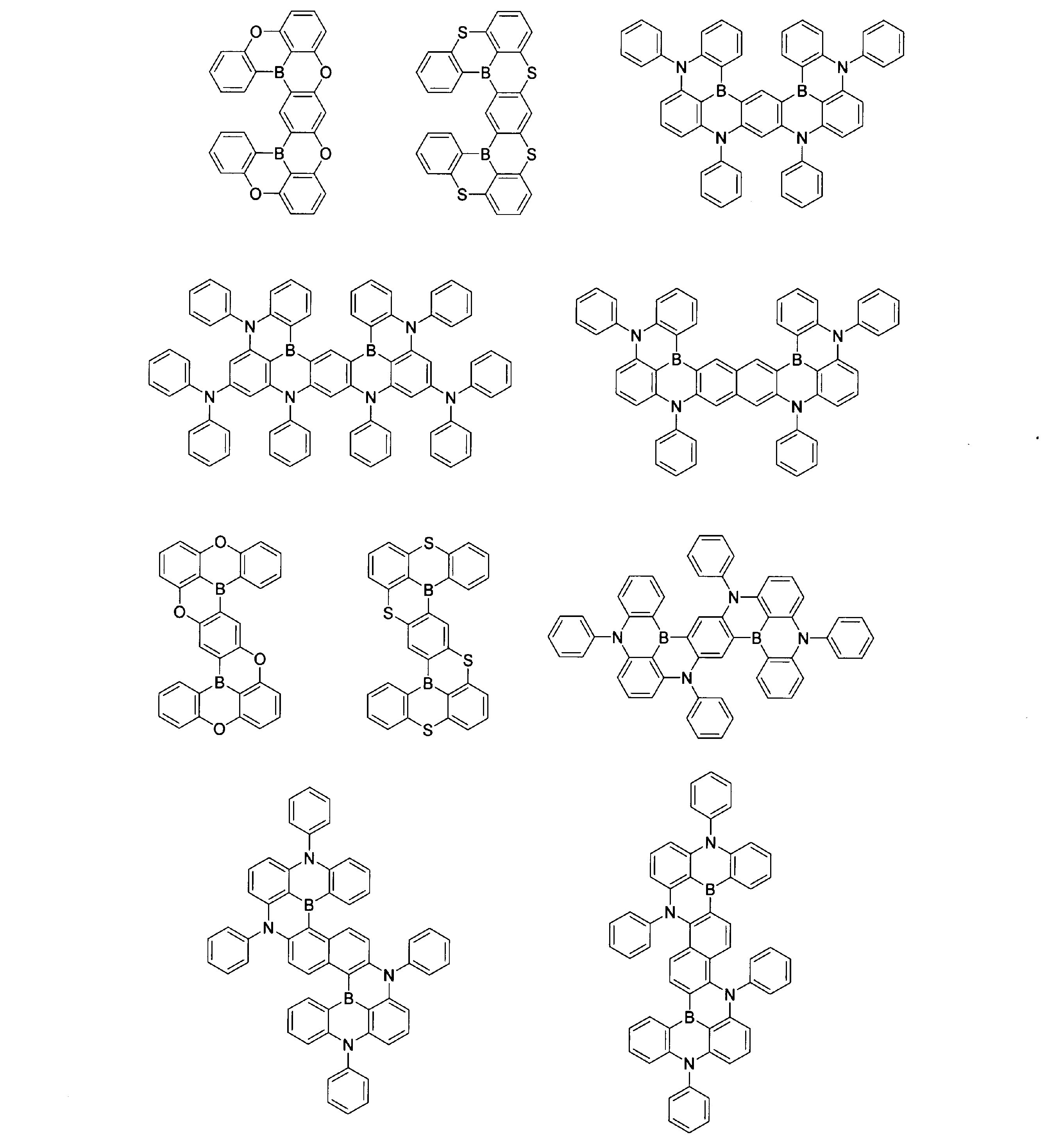
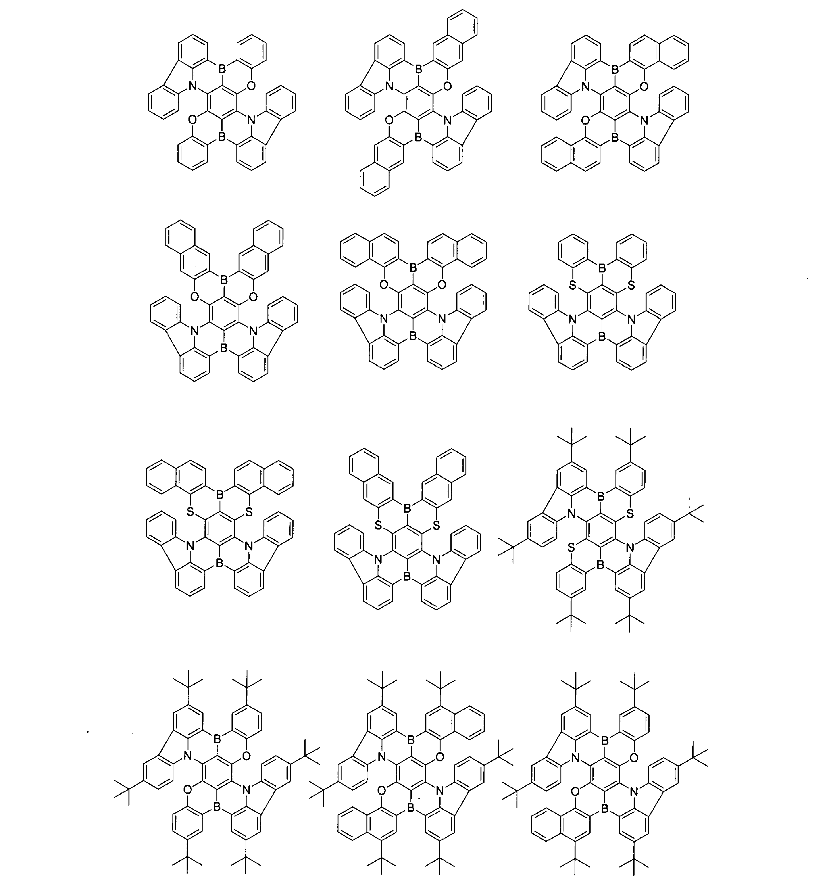
一般式(1)で表される構造を有する化合物、および一般式(1)で表される構造を有する多量体は、公知の方法、例えば、国際公開第2015/102118号、特開2021-063067号公報に記載されている方法等により合成することができる。
一般式(1)で表される構造を有する化合物、および一般式(1)で表される構造を有する多量体は、再結晶やカラムクロマトグラフィーなどの有機合成的な精製を行った後、さらに、一般的に昇華精製と呼ばれる減圧加熱による精製により低沸点成分を除去し、純度を向上させることが好ましい。昇華精製における加熱温度は、熱分解を防ぐ観点から、400℃以下が好ましく、380℃以下がより好ましく、360℃以下がさらに好ましい。
一般式(1)で表される構造を有する化合物、および一般式(1)で表される構造を有する多量体の純度は、光電変換特性の安定化の観点から、99重量%以上であることが好ましい。
(光センサの構成)
本発明の光センサの素子構成としては、例えば、陽極/光電変換層/陰極、陽極/正孔輸送層/光電変換層/陰極、陽極/正孔輸送層/光電変換層/電子輸送層/陰極、陽極/正孔取り出し層/光電変換層/陰極、陽極/正孔取り出し層/光電変換層/電子輸送層/陰極、陽極/正孔取り出し層/正孔輸送層/光電変換層/電子輸送層/陰極、陽極/正孔取り出し層/正孔輸送層/光電変換層/電子輸送層/電子取り出し層/陰極といった構成が挙げられる。
本発明の光センサの素子構成としては、例えば、陽極/光電変換層/陰極、陽極/正孔輸送層/光電変換層/陰極、陽極/正孔輸送層/光電変換層/電子輸送層/陰極、陽極/正孔取り出し層/光電変換層/陰極、陽極/正孔取り出し層/光電変換層/電子輸送層/陰極、陽極/正孔取り出し層/正孔輸送層/光電変換層/電子輸送層/陰極、陽極/正孔取り出し層/正孔輸送層/光電変換層/電子輸送層/電子取り出し層/陰極といった構成が挙げられる。
光電変換層は、2種類以上の光電変換材料を含むことが好ましく、例えば、本発明の一般式(1)で表される構造を有する化合物、または一般式(1)で表される構造を有する多量体と、その他の光電変換材料とを組み合わせることが好ましい。組み合わせる光電変換材料としては、p型またはn型の半導体特性を示す有機半導体が好ましい。一般式(1)で表される構造を有する化合物、または一般式(1)で表される構造を有する多量体は正孔輸送性のp型半導体特性を示すため、光電変換層がさらにn型の半導体特性を示すn型有機半導体を含有することがより好ましい。
n型有機半導体としては、例えば1,4,5,8-ナフタレンテトラカルボキシリックジアンハイドライド(NTCDA)、3,4,9,10-ペリレンテトラカルボキシリックジアンハイドライド(PTCDA)、3,4,9,10-ペリレンテトラカルボキシリックビスベンズイミダゾール(PTCBI)、N,N'-ジオクチル-3,4,9,10-ナフチルテトラカルボキシジイミド(PTCDI-C8H)、2-(4-ビフェニリル)-5-(4-t-ブチルフェニル)-1,3,4-オキサジアゾール(PBD)、2,5-ジ(1-ナフチル)-1,3,4-オキサジアゾール(BND)等のオキサゾール誘導体、3-(4-ビフェニリル)-4-フェニル-5-(4-t-ブチルフェニル)-1,2,4-トリアゾール(TAZ)等のトリアゾール誘導体、フェナントロリン誘導体、ホスフィンオキサイド誘導体、ナフタレンテトラカルボン酸ジイミド誘導体、フラーレン化合物、カーボンナノチューブ(CNT)、ポリ-p-フェニレンビニレン系重合体にシアノ基を導入した誘導体(CN-PPV)などが挙げられる。これらを2種以上用いてもよい。
中でも、フラーレン化合物は電荷分離速度と電子移動速度が速いため、好ましく用いられる。フラーレン化合物としては、C60、C70、C76、C78、C82、C84、C90、C94を始めとする無置換のもの、[6,6]-フェニル C61 ブチリックアシッドメチルエステル([6,6]-PCBM)、[5,6]-フェニル C61 ブチリックアシッドメチルエステル([5,6]-PCBM)、[6,6]-フェニル C61 ブチリックアシッドヘキシルエステル([6,6]-PCBH)、[6,6]-フェニル C61 ブチリックアシッドドデシルエステル([6,6]-PCBD)、フェニル C71 ブチリックアシッドメチルエステル(PC70BM)、フェニル C85 ブチリックアシッドメチルエステル(PC84BM)などが挙げられる。
p型有機半導体としては、例えば、ターチオフェン、クウォーターチオフェン、セキシチオフェン、オクチチオフェンなどのオリゴチオフェン化合物、フェニレンビニレン系化合物、p-フェニレン系化合物、ポリフルオレン系化合物、化合物H2フタロシアニン(H2Pc)、銅フタロシアニン(CuPc)、亜鉛フタロシアニン(ZnPc)等のフタロシアニン誘導体、ポルフィリン誘導体、N,N’-ジフェニル-N,N’-ジ(3-メチルフェニル)-4,4’-ジフェニル-1,1’-ジアミン(TPD)、N,N’-ジナフチル-N,N’-ジフェニル-4,4’-ジフェニル-1,1’-ジアミン(NPD)等のトリアリールアミン誘導体、4,4’-ジ(カルバゾール-9-イル)ビフェニル(CBP)等のカルバゾール誘導体などが挙げられる。これらを2種以上用いてもよい。
上記のように、一般式(1)で表される構造を有する化合物または一般式(1)で表される構造を有する多量体と、HOMOやLUMO(Lowest unoccupied Molecular Orbital)のエネルギー準位が異なる有機半導体と組み合わせることにより、光を吸収して生成する励起子が異種材料界面で効率的に電荷分離・電荷解離するため、光電変換効率をより高めることができる。
光電変換層が2種類以上の光電変換材料を含む場合、これらの材料は一層の中で混合されていてもよいし、各光電変改材料を含む層が積層されていてもよいが、整流性の観点から、積層されていることが好ましい。
積層されている場合は、p型有機半導体を含む層が陽極側、n型有機半導体を含む層が陰極側に位置することが好ましい。また、積層されている場合、積層界面に混合層(i層)を有してもよい。このような構成はp-i-n構造と呼ばれており、i層が主に電荷分離を担い、p層とn層がそれぞれ主に正孔輸送と電子輸送を担うことにより、光電変換効率をより高めることができる。
混合されている場合は、一般式(1)で表される構造を有する化合物または一般式(1)で表される構造を有する多量体と組み合わせる材料が分子レベルで相溶しているか、もしくは、ナノレベルで相分離していることが好ましい。相分離している場合、相分離構造のドメインサイズは、1nm以上50nm以下が好ましい。
光電変換層の厚さは、10nm~500nmが好ましく、より好ましくは20nm~100nmである。光電変換層が積層構造からなる場合は、上記光電変換層全体の厚さのうち、一般式(1)で表される構造を有する化合物または一般式(1)で表される構造を有する多量体を含む層の厚さおよび積層される層の厚さは、それぞれ5nm~495nmが好ましく、より好ましくは10nm~50nmである。積層界面に混合層(i層)を有する場合、i層の厚さは、1nm~100nmが好ましく、より好ましくは5nm~50nmである。
光センサにおいては、陽極および/または陰極が光透過性を有することが好ましい。電極の光透過率は、光電変換層に入射光が到達して起電力が発生する程度であれば、特に限定されるものではない。ここで、光透過率とは、[透過光強度(W/m2)/入射光強度(W/m2)]×100(%)で求められる値である。光透過性を有する電極の厚さは、光透過性と導電性とを有する範囲であればよく、電極素材によって異なるが、20nm~300nmが好ましい。なお、もう一方の電極は、導電性があれば必ずしも光透過性は必要ではなく、厚さも特に限定されない。
電極材料としては、一方の電極には仕事関数の大きな導電性素材、もう一方の電極には仕事関数の小さな導電性素材を使用することが好ましい。
仕事関数の大きな導電性素材を用いた電極は陽極となる。仕事関数の大きな導電性素材としては、例えば、金、白金、クロム、ニッケルなどの金属のほか、透明性を有するインジウム、スズ、モリブデンなどの金属酸化物、インジウム錫酸化物(ITO)、インジウム亜鉛酸化物(IZO)などの複合金属酸化物などが好ましく用いられる。ここで、陽極に用いられる導電性素材は、光電変換層とオーミック接合するものであることが好ましい。さらに、後述するように、陽極と光電変換層の間に正孔輸送層を設けた場合においては、陽極に用いられる導電性素材は、正孔輸送層とオーミック接合するものであることが好ましい。陽極の形成方法は、その形成材料に応じて最適な方法を選択することができるが、例えば、スパッタ法、蒸着法、インクジェット法などが挙げられる。例えば、金属酸化物によって陽極を形成する場合にはスパッタ法、金属によって陽極を形成する場合には蒸着法が好ましく用いられる。
仕事関数の小さな導電性素材を用いた電極は陰極となる。仕事関数の小さな導電性素材としては、例えば、リチウムなどのアルカリ金属、マグネシウム、カルシウムなどのアルカリ土類金属、錫や銀、アルミニウムなどや、これらの合金などが好ましく用いられる。これらを2種以上用いた積層体であってもよい。ここで、陰極に用いられる導電性素材は、光電変換層とオーミック接合するものであることが好ましい。さらに、後述するように、陰極と光電変換層の間に電子輸送層を設けた場合においては、陰極に用いられる導電性素材は、電子輸送層とオーミック接合するものであることが好ましい。また、陰極と電子輸送層の界面に、フッ化リチウムやフッ化セシウムなどの金属フッ化物を導入することにより、取り出し電流を向上させることも可能である。
光センサの機械的強度を保ち、熱変形を抑制し、光電変換層への水蒸気や酸素の侵入を抑制するバリア性を付与するために、光センサを基板上に形成することが好ましい。基板としては、例えば、ガラス板、セラミック板、樹脂フィルム、ワニスを硬化した樹脂薄膜、金属製薄板などが挙げられる。これらの中でも、透明であり、加工が容易である観点から、ガラス基板が好適に用いられる。また、主にスマートフォンなどのモバイル機器において、フレキシブルディスプレイやフォルダブルディスプレイが増加しており、この用途には、樹脂フィルムや樹脂薄膜が好適例えば、ポリイミドフィルム、ポリエチレンナフタレートフィルムなどの耐熱フィルムが挙げられる。
本発明の光センサは、陽極と光電変換層の間に正孔輸送層および/または正孔取り出し層を有することが好ましい。正孔輸送層を形成する材料としては、例えば、オリゴチオフェン化合物、フェニレンビニレン系化合物、p-フェニレン系化合物、ポリフルオレン系化合物、H2フタロシアニン(H2Pc)、銅フタロシアニン(CuPc)、亜鉛フタロシアニン(ZnPc)等のフタロシアニン誘導体、ポルフィリン誘導体、N,N’-ジフェニル-N,N’-ジ(3-メチルフェニル)-4,4’-ジフェニル-1,1’-ジアミン(TPD)、N,N’-ジナフチル-N,N’-ジフェニル-4,4’-ジフェニル-1,1’-ジアミン(NPD)等のアリールアミン誘導体、4,4’-ジ(カルバゾール-9-イル)ビフェニル(CBP)、N-[1,1’-ビフェニル]-4-イル-9,9-ジメチル-N-[4-(9-フェニル-9H-カルバゾール-3-イル)フェニル]-9H-フルオレン-2-アミン等のカルバゾール誘導体や、酸化モリブデン、酸化タングステンなどのp型半導体性を示す金属酸化物が挙げられるが、良好な正孔輸送性を有するという観点では、アリールアミン誘導体またはカルバゾール誘導体が好ましい。正孔輸送層の厚さは、1nm~200nmが好ましく、より好ましくは5nm~100nmである。正孔輸送層はいくつかの材料が積層されていてもよく、また2種以上の材料を混合して用いてもよい。
正孔取り出し層を形成する材料としては、例えば、トリス(4-ブロモフェニル)アミニウムヘキサクロロアンチモネート(TBPAH)などの電荷移動錯体、7,7,8,8-テトラシアノキノジメタン(TCNQ)、2,3,5,6-テトラフルオロ-7,7,8,8-テトラシアノキノジメタン(F4-TCNQ)、2,3,6,7,10,11-ヘキサシアノ-1,4,5,8,9,12-ヘキサアザトリフェニレン(HAT-CN6)などのハロゲン原子および/またはシアノ基を含有する化合物、フッ素化銅フタロシアニン、またはポリ4-スチレンスルホン酸をドープしたポリ3,4-エチレンジオキシチオフェン(PEDOT:PSS)などの導電性高分子が挙げられる。これらを2種以上含んでもよい。中でも正孔取り出し層は、ハロゲン原子および/またはシアノ基を含有する化合物を含むことが好ましい。すなわち、本発明の光センサは、光電変換層と陽極の間に正孔取り出し層を有し、正孔取り出し層がハロゲン原子および/またはシアノ基を含有する化合物を含むことが好ましい。光センサは、有機薄膜太陽電池と異なり、通常、電圧が印加された状態で光検出に用いられるため、光センサの誤作動防止の観点で、光を照射していない場合に流れる暗電流を極力低減することが求められる。正孔取り出し層がハロゲン原子および/またはシアノ基を含有する化合物を含むことにより、高い光電変換効率を維持しながら、暗電流を低減することができる。
ハロゲン原子および/またはシアノ基を含有する化合物は、正孔取り出し層中に単独で用いられていても、ドーパントとしてドープされていてもよい。単独で用いられる場合は、正孔取り出し層が隣接する有機層に含まれる材料との間で電荷移動錯体を形成することが好ましい。またドープされている場合は、正孔取り出し層中のホスト材料および/または正孔取り出し層が隣接する有機層に含まれる材料との間で電荷移動錯体を形成することが好ましい。
以上の観点から、ハロゲン原子および/またはシアノ基を含有する化合物がドープされている場合は、正孔取り出し層中のホスト材料として上述の正孔輸送層を形成する材料が用いられ、その中にドープされていることが好ましく、中でもアリールアミン誘導体またはカルバゾール誘導体にドープされていることがより好ましい。
また、ハロゲン原子および/またはシアノ基を含有する化合物に含まれるハロゲン原子としては、電荷移動錯体を形成しやすいという観点で、最も電気陰性度の大きいフッ素原子が好ましい。
さらにハロゲン原子および/またはシアノ基を含有する化合物が一般式(2)で表される化合物である場合、電荷移動錯体形成能力がより大きくなるため好ましい。

上記一般式(2)中、R1~R6はそれぞれ同一でも異なっていても良く、置換もしくは無置換のアリール基、置換もしくは無置換のヘテロアリール基、シアノ基、ニトロ基、ハロゲン原子およびハロゲン化アルキル基からなる群より選ばれる。ただし、R1~R6のうち少なくとも1つはシアノ基またはハロゲン原子である。
蒸着時の耐熱性と蒸着膜における配向性の観点から、R1~R6の少なくとも1つは、置換もしくは非置換のアリール基または置換もしくは非置換のヘテロアリール基が好ましい。中でも、R1、R3およびR5がそれぞれ独立に置換もしくは非置換のアリール基または置換もしくは非置換のヘテロアリール基であり、R2、R4およびR6がそれぞれ独立にシアノ基またはハロゲン原子であることがより好ましい。またハロゲン原子としては、電荷移動錯体形成能力がより大きくなるという観点でフッ素原子が好ましい。
以下に一般式(2)で表される構造を有する化合物の例を示すが、これらに限定されるものではない。
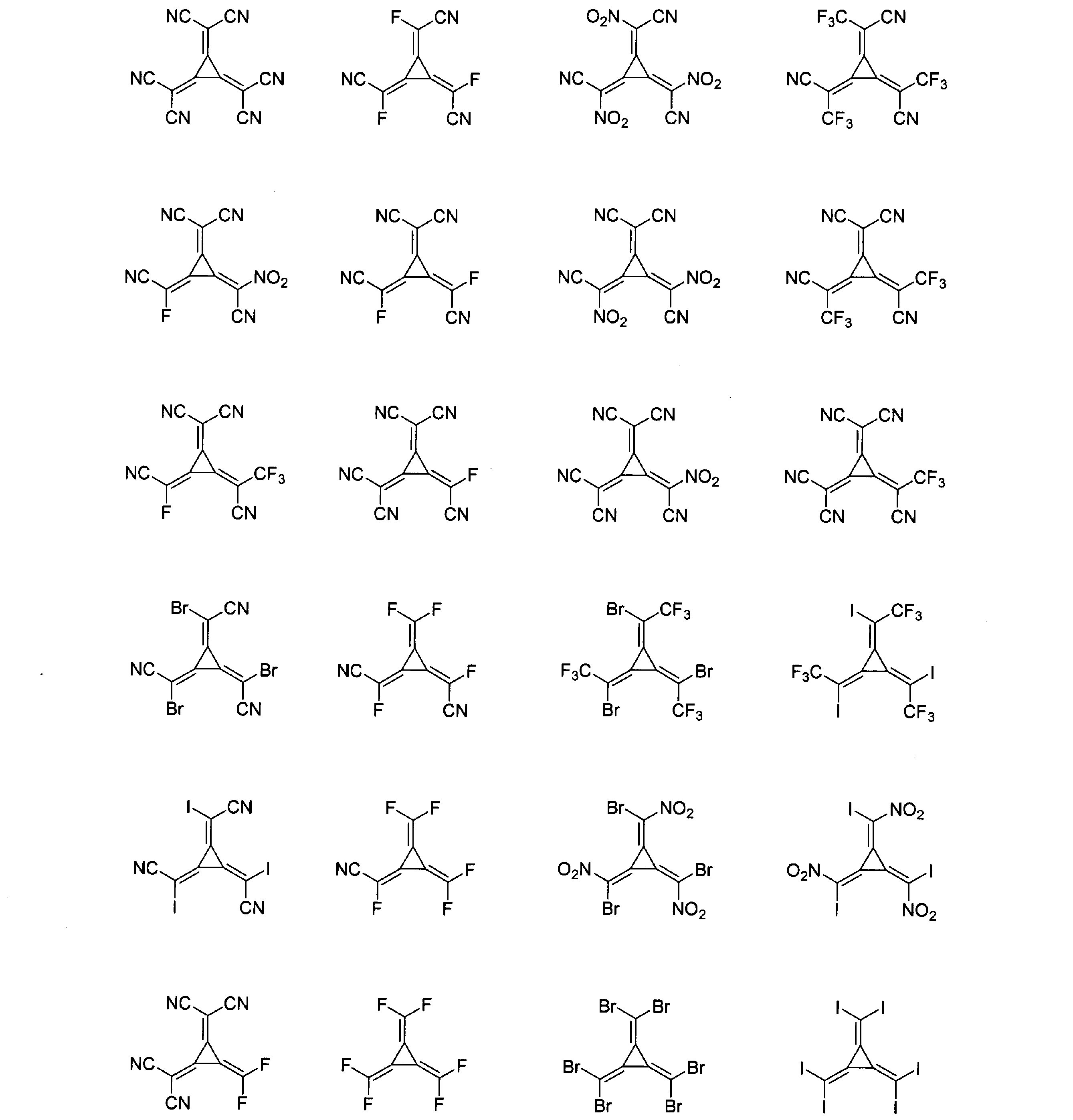
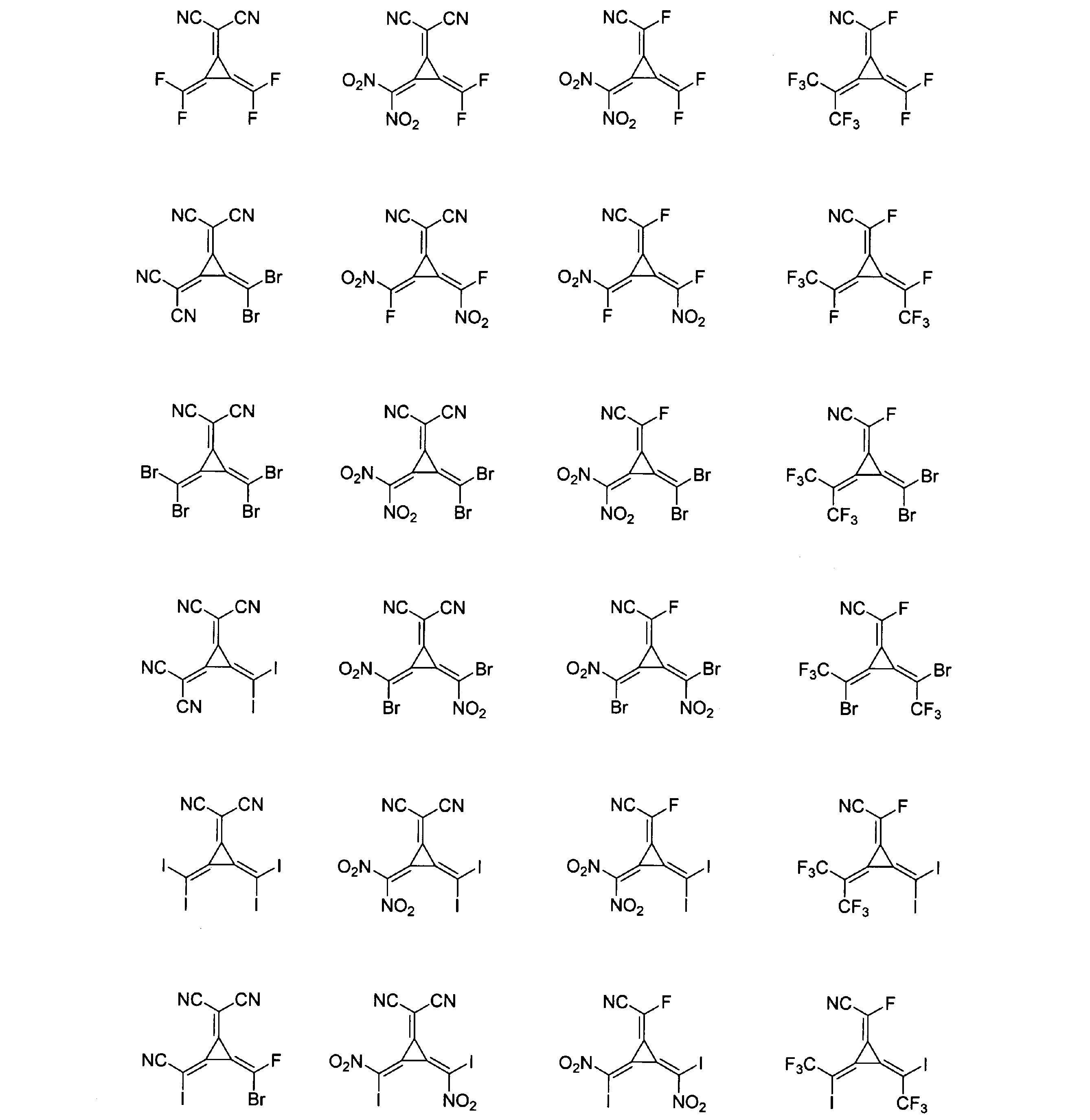


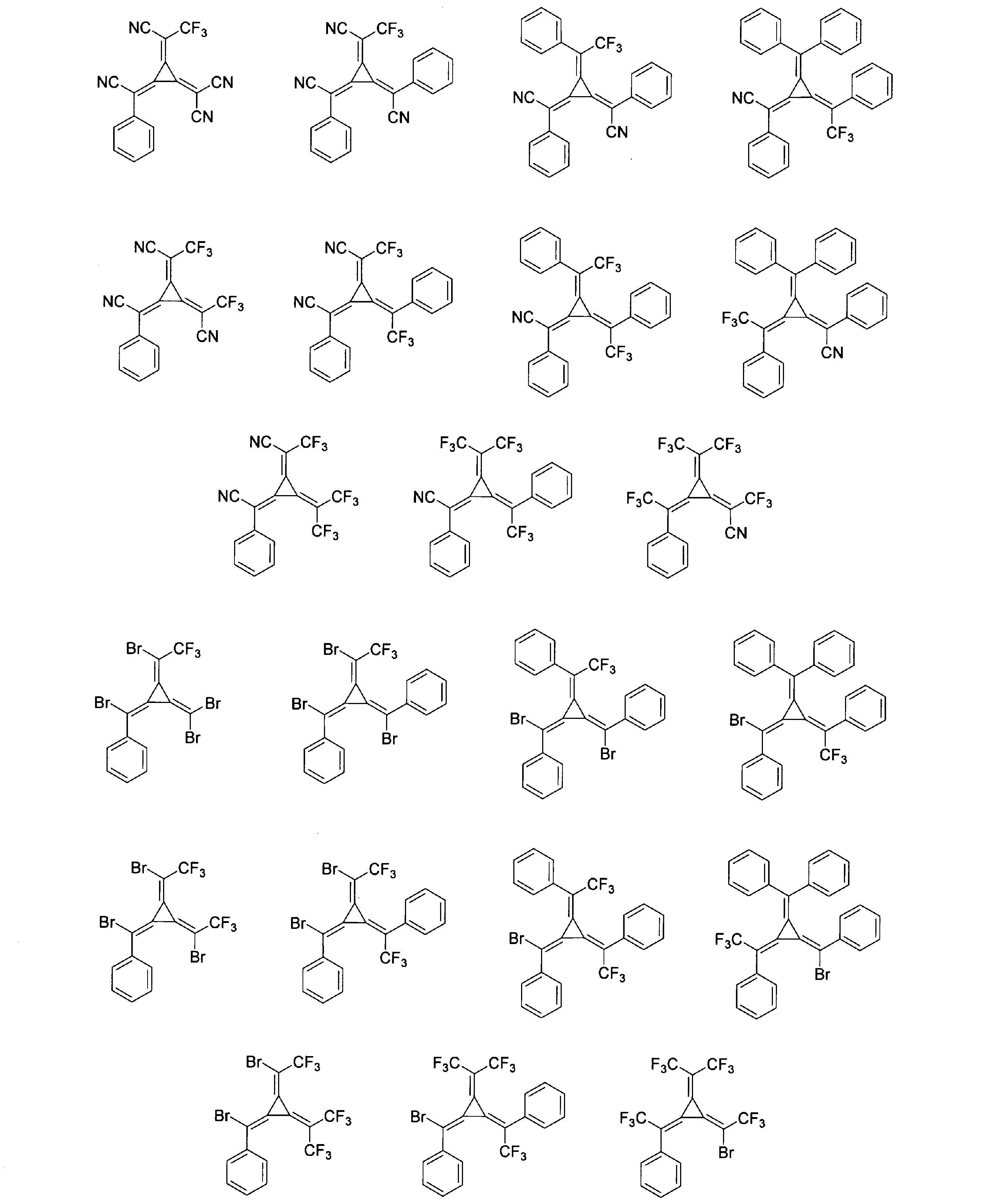
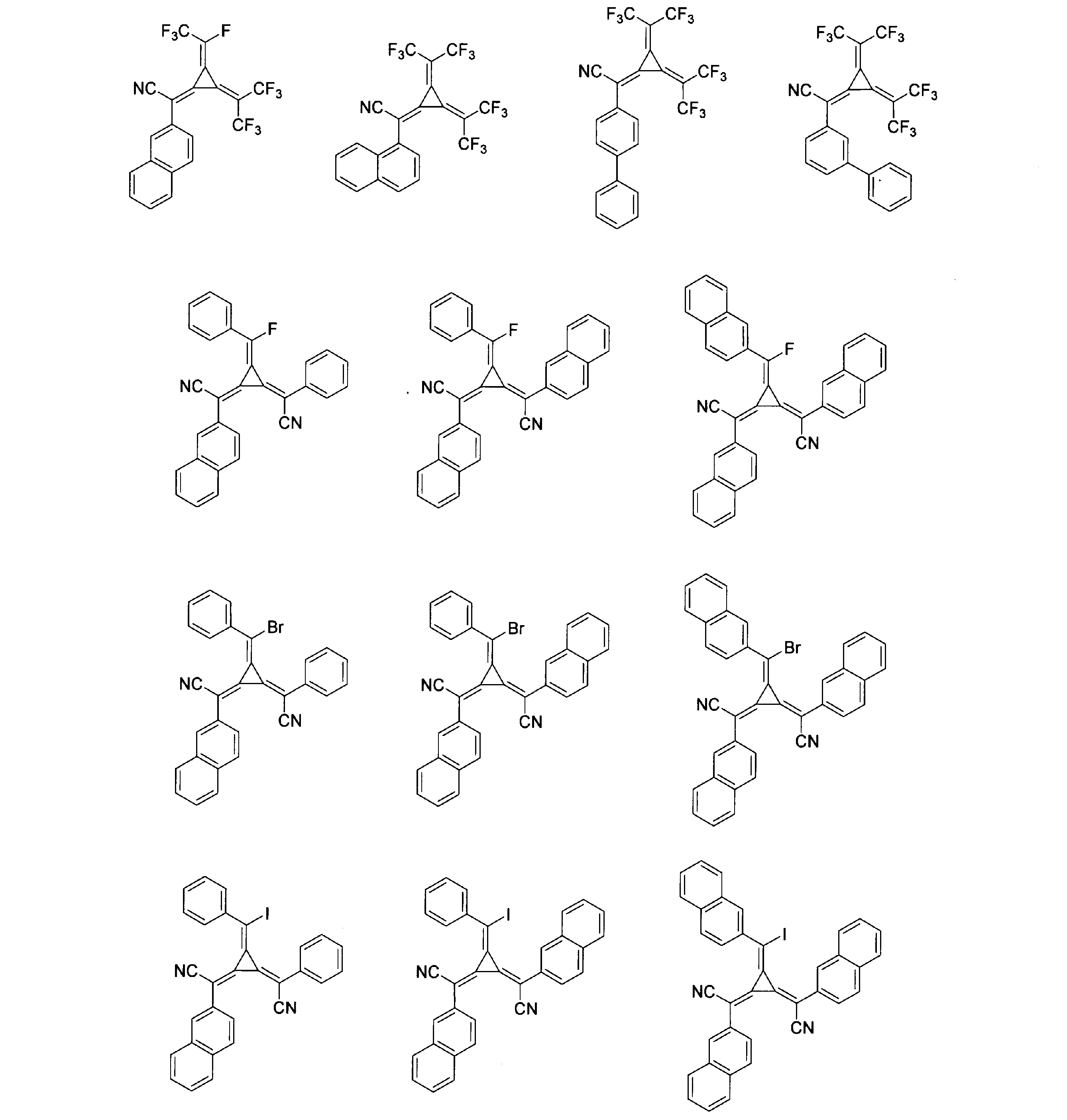

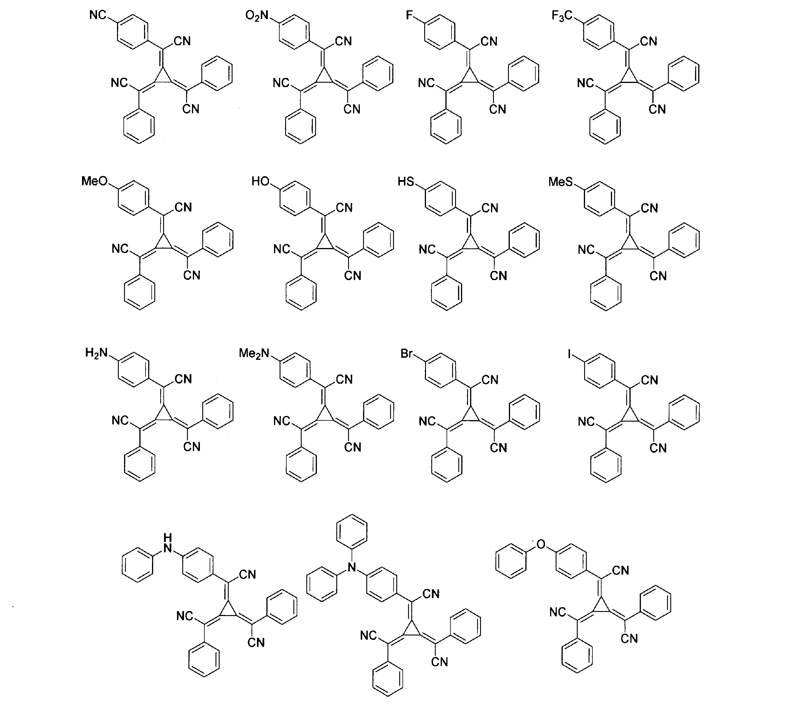
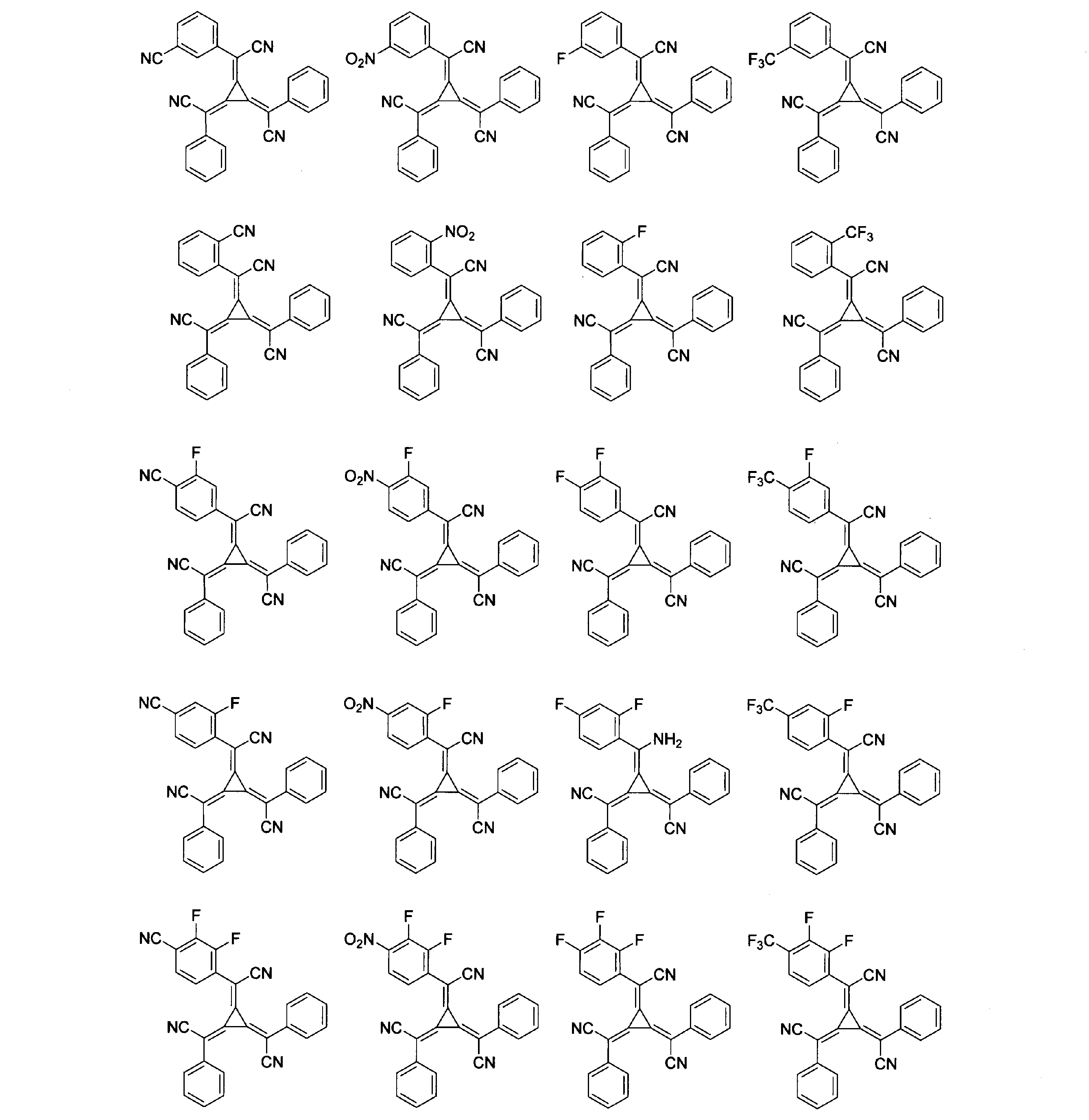
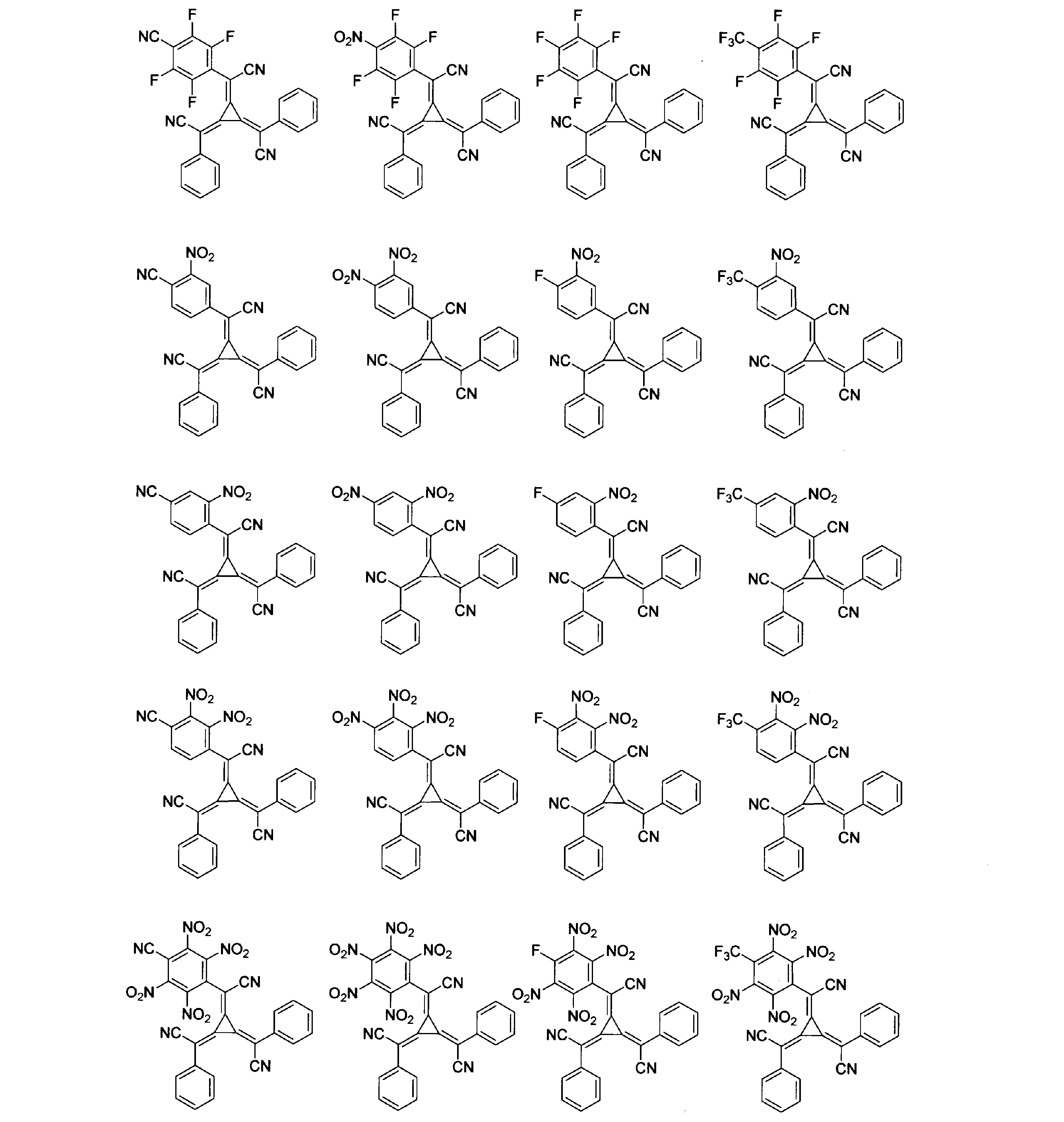

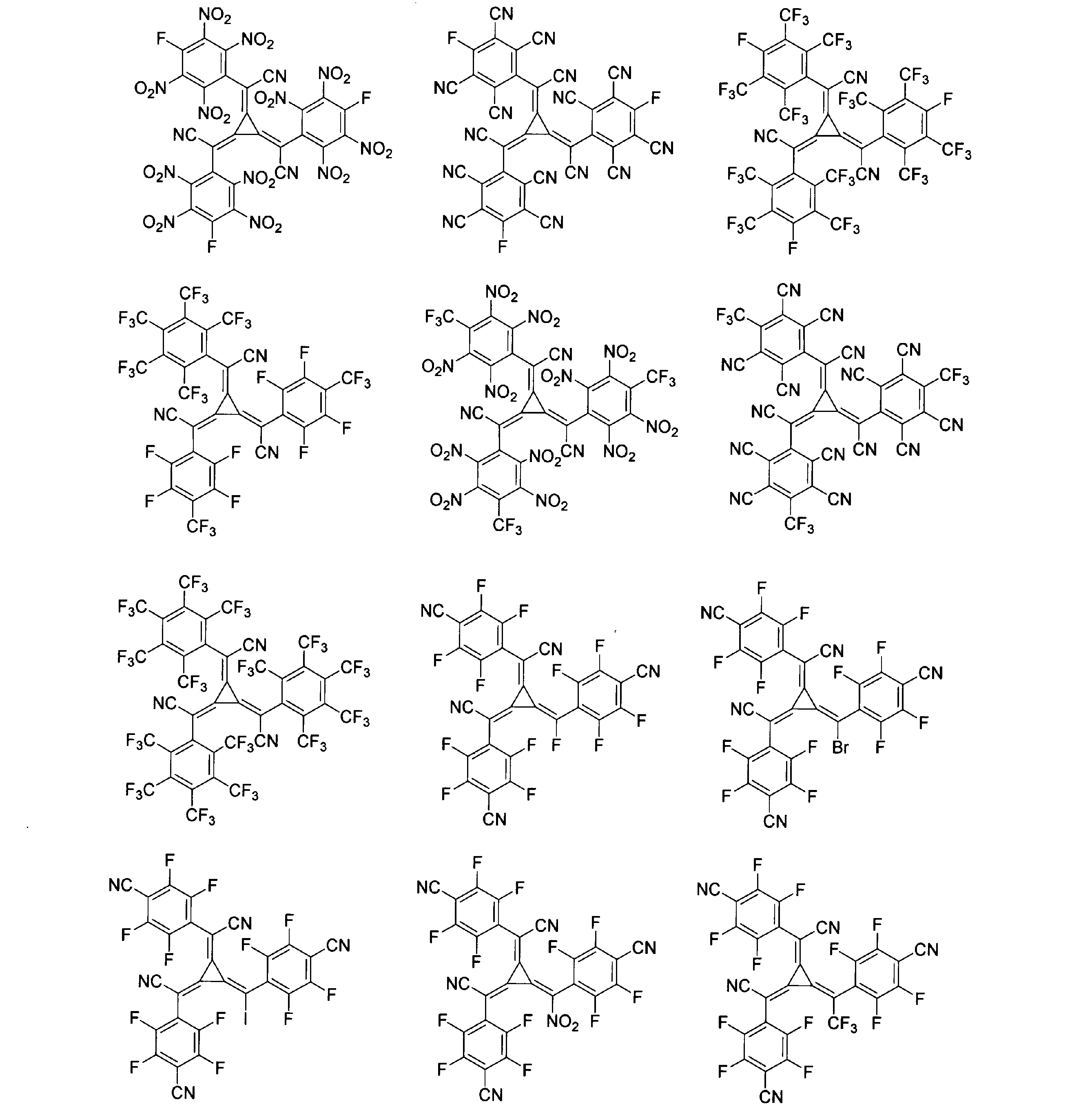
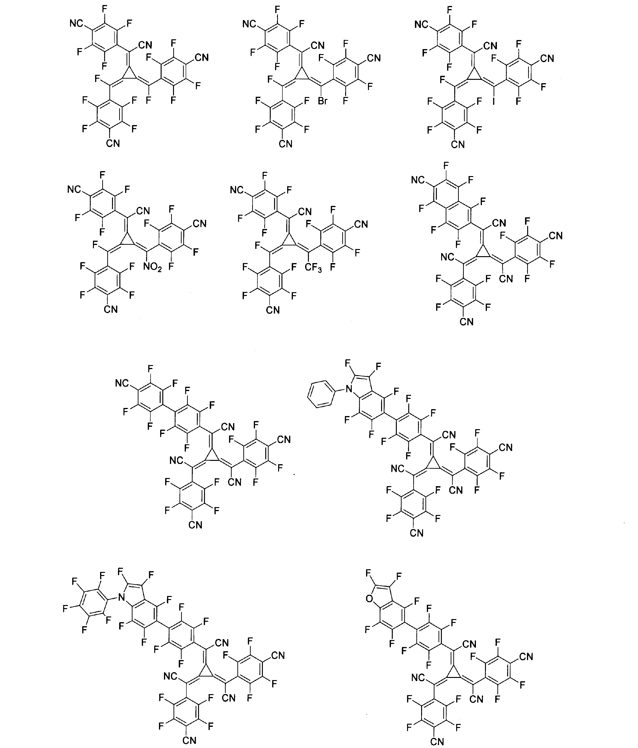
正孔取り出し層の厚さは、1nm~200nmが好ましく、より好ましくは5nm~100nmである。また正孔取り出し層は陽極に接していることが好ましい。
本発明の光センサは、光電変換層と陰極の間に電子輸送層および/または電子取り出し層を有していてもよい。電子輸送層および/または電子取り出し層に用いられる電子輸送材料および/または電子取り出し材料としては、例えば、上述のn型半導体材料や、多環芳香族誘導体、スチリル系芳香環誘導体、キノン誘導体、リンオキサイド誘導体、トリス(8-キノリノラート)アルミニウム(III)などのキノリノール錯体、ベンゾキノリノール錯体、ヒドロキシアゾール錯体、アゾメチン錯体、トロポロン金属錯体およびフラボノール金属錯体などの各種金属錯体が挙げられる。これらを2種以上含んでもよい。
電子輸送効率をより向上させる観点から、電子輸送層および/または電子取り出し層には電子受容性窒素を含むヘテロアリール基を有する化合物を用いることが好ましい。ここで、電子受容性窒素とは、隣接原子との間に多重結合を形成している窒素原子を表す。電子受容性窒素を含むヘテロアリール基は、電子親和力が大きいため、電子を輸送しやすくなり、光電変換効率をより高めることができる。
電子受容性窒素を含むヘテロアリール基を有する化合物としては、例えば、ピリジン誘導体、トリアジン誘導体、ピラジン誘導体、ピリミジン誘導体、キノリン誘導体、キノキサリン誘導体、キナゾリン誘導体、ナフチリジン誘導体、ベンゾキノリン誘導体、フェナントロリン誘導体、イミダゾール誘導体、オキサゾール誘導体、チアゾール誘導体、トリアゾール誘導体、オキサジアゾール誘導体、チアジアゾール誘導体、ベンズイミダゾール誘導体、ベンズオキサゾール誘導体、ベンズチアゾール誘導体、フェナンスロイミダゾール誘導体、ビピリジンやターピリジンなどのオリゴピリジン誘導体などが挙げられる。また、電子輸送材料が縮合多環芳香族骨格を有していると、ガラス転移温度が向上し、電子移動度が大きいためより好ましい。このような縮合多環芳香族骨格としては、キノリノール錯体、トリアジン誘導体、フルオランテン骨格、アントラセン骨格、ピレン骨格またはフェナントロリン骨格などが挙げられる。
電子輸送層は、電子ドナー性材料を含んでもよい。ここで、電子ドナー性材料とは、電子輸送層の電気伝導性を向上させる化合物である。電子ドナー性材料の好ましい例としては、Liなどのアルカリ金属、LiFなどのアルカリ金属を含有する無機塩、リチウムキノリノールなどのアルカリ金属と有機物との錯体、アルカリ土類金属、アルカリ土類金属を含有する無機塩、アルカリ土類金属と有機物との錯体、EuやYbなどの希土類金属、希土類金属を含有する無機塩、希土類金属と有機物との錯体などが挙げられる。これらを2種以上含んでもよい。これらの中でも、金属リチウム、希土類金属、リチウムキノリノール(Liq)が好ましい。
電子輸送層および電子取出し層の厚さは、1nm~200nmが好ましく、より好ましくは3nm~100nmである。
本発明の光センサを構成する上記各層の形成方法は、ドライプロセスまたはウェットプロセスのいずれでもよく、例えば、抵抗加熱蒸着、電子ビーム蒸着、スパッタリング、分子積層法、コーティング法、インクジェット法、印刷法などが挙げられる。これらの中でも、素子特性の観点から、抵抗加熱蒸着が好ましい。一方、高分子材料を用いる場合は、適当な溶媒を用いたコーティング法が好ましい。
本発明の光センサは、例えば、指紋、静脈、脈波、血中酸素濃度等の生体情報を高感度で検知することができる他、環境の明るさに係る照度、リモコンやスイッチに関連する光信号、動植物や自動車等の物体に関わる情報を高感度に検出できる。これらの中でも本発明の光センサは生体情報の検知に適する。
また、本発明の光センサは、本発明の光センサと有機発光素子とを有し、有機発光素子の光を利用して対象情報を検知する表示装置に利用することができる。すなわち、本発明の表示装置は、本発明の光センサと有機発光素子とを有し、有機発光素子の光を利用して対象情報を検知する表示装置である。例えば、マトリクスおよび/またはセグメント方式で表示する有機ELディスプレイの画素の一部を、本発明の光センサとして構成することにより、有機ELディスプレイに指紋認証機能を付与することができる。例えば、有機ELディスプレイの有機発光素子から発せられる光がディスプレイに触れた指により反射・散乱された光を、本発明の光センサにより受光・光電変換することにより、指紋情報や静脈情報などの生体情報を高精度に取得することができる。すなわち、対象情報が指紋情報であることが好ましい。また、対象情報が静脈情報であることが好ましい。
以下、実施例を挙げて本発明を説明するが、本発明はこれらの例によって限定されるものではない。まず、各実施例および比較例における評価方法を以下に記載する。
(光電変換効率)
各実施例および比較例によって得られた光センサについて、大気中、ガラス基板側から波長350~700nmの可視光を照射し、分光感度測定装置(分光計器(株)製、ハイパーモノライトシステム、SM-250型)を用いて、印加電圧を-3Vとしたときの光電変換効率とその時の電流値I-Photo[A]を測定した。
各実施例および比較例によって得られた光センサについて、大気中、ガラス基板側から波長350~700nmの可視光を照射し、分光感度測定装置(分光計器(株)製、ハイパーモノライトシステム、SM-250型)を用いて、印加電圧を-3Vとしたときの光電変換効率とその時の電流値I-Photo[A]を測定した。
(暗電流測定)
得られた光センサについて、大気中でセンサを黒色シートで覆い、KEITHLEY2400(Tektronix社製)を用いて、-3Vにおける暗電流値I-Dark[A]を測定し、I-PhotoをI-Darkで割った値I-Photo/I-Darkを求め、光センサの感度を評価した。
得られた光センサについて、大気中でセンサを黒色シートで覆い、KEITHLEY2400(Tektronix社製)を用いて、-3Vにおける暗電流値I-Dark[A]を測定し、I-PhotoをI-Darkで割った値I-Photo/I-Darkを求め、光センサの感度を評価した。
(実施例1)
陽極としてITO電極層を125nm有する、46mm×38mmの透明ガラス基板を用意した。この基板を、アルカリ洗浄液(フルウチ化学(株)製、“セミコクリーン”EL56)を純水で10倍希釈した希釈液に浸し、10分間超音波洗浄した後、純水による5分間の超音波洗浄を2度行い、十分に乾燥した。その後、UVオゾン洗浄を30分間行った。
陽極としてITO電極層を125nm有する、46mm×38mmの透明ガラス基板を用意した。この基板を、アルカリ洗浄液(フルウチ化学(株)製、“セミコクリーン”EL56)を純水で10倍希釈した希釈液に浸し、10分間超音波洗浄した後、純水による5分間の超音波洗浄を2度行い、十分に乾燥した。その後、UVオゾン洗浄を30分間行った。
続いて、基板のITO電極層上に、ポリ4-スチレンスルホン酸をドープしたポリ3,4-エチレンジオキシチオフェン(PEDOT:PSS)とイソプロピルアルコールを体積比6:4で混合した溶液を、3,000rpmで30秒間スピンコートし、150℃のホットプレートで10分間、加熱処理し、厚さ55nmの正孔取り出し層を形成した。
続いて洗浄した基板を、真空蒸着装置((株)エイコー・エンジニアリング製)に設置し、約3×10⁻³Paまで減圧した後、正孔輸送層としてN-[1,1’-ビフェニル]-4-イル-9,9-ジメチル-N-[4-(9-フェニル-9H-カルバゾール-3-イル)フェニル]-9H-フルオレン-2-アミン(化合物1、膜厚40nm)、光電変換層のp型半導体としてホウ素化合物(化合物A-1、膜厚15nm)、n型半導体としてフラーレン(化合物2、膜厚15nm)を順に蒸着し、正孔輸送層と光電変換層をそれぞれ形成した。真空蒸着装置を一度大気開放した後、蒸着源を入れ替え、再び約3×10⁻³Paまで減圧した。光電変換層上に、リチウムキノリノール錯体(化合物3、膜厚5nm)とアルミニウム(膜厚31nm)を順次蒸着し、電子輸送層と陰極をそれぞれ形成した。得られた積層体を、グローブボックス内において、バリアフィルム(TESA製)により封止し、光センサを得た。
(実施例2)
化合物A-1の代わりに化合物A-2を使用したことと、アルミニウムの膜厚を54nmに変更したこと以外、実施例1と同様にして光センサを得た。
化合物A-1の代わりに化合物A-2を使用したことと、アルミニウムの膜厚を54nmに変更したこと以外、実施例1と同様にして光センサを得た。
(実施例3)
化合物A-1の代わりに化合物A-3を使用したことと、アルミニウムの膜厚を72nmに変更したこと以外、実施例1と同様に光センサを得た。
化合物A-1の代わりに化合物A-3を使用したことと、アルミニウムの膜厚を72nmに変更したこと以外、実施例1と同様に光センサを得た。
(実施例4)
化合物A-1の代わりに化合物A-4を使用したことと、アルミニウムの膜厚を43nmに変更したこと以外、実施例1と同様に光センサを得た。
化合物A-1の代わりに化合物A-4を使用したことと、アルミニウムの膜厚を43nmに変更したこと以外、実施例1と同様に光センサを得た。
(実施例5)
化合物A-1の代わりに化合物A-5を使用したことと、アルミニウムの膜厚を38nmに変更したこと以外、実施例1と同様に光センサを得た。
化合物A-1の代わりに化合物A-5を使用したことと、アルミニウムの膜厚を38nmに変更したこと以外、実施例1と同様に光センサを得た。
(実施例6)
化合物A-1の代わりに化合物A-6(純度85%)を使用したことと、アルミニウムの膜厚を72nmに変更したこと以外、実施例1と同様に光センサを得た。
化合物A-1の代わりに化合物A-6(純度85%)を使用したことと、アルミニウムの膜厚を72nmに変更したこと以外、実施例1と同様に光センサを得た。
(実施例7)
化合物1で形成される正孔輸送層に対して正孔取り出し層に用いられる、フッ素原子およびシアノ基を構造中に含む化合物4を5%ドープさせたこと、アルミニウムの膜厚を42nmに変更したこと以外、実施例3と同様に光センサを得た。
化合物1で形成される正孔輸送層に対して正孔取り出し層に用いられる、フッ素原子およびシアノ基を構造中に含む化合物4を5%ドープさせたこと、アルミニウムの膜厚を42nmに変更したこと以外、実施例3と同様に光センサを得た。
(実施例8)
化合物1で形成される正孔輸送層に対して正孔取り出し層に用いられる、フッ素原子およびシアノ基を構造中に含む化合物4を3%ドープさせたこと、アルミニウムの膜厚を19nmに変更したこと以外、実施例5と同様に光センサを得た。
化合物1で形成される正孔輸送層に対して正孔取り出し層に用いられる、フッ素原子およびシアノ基を構造中に含む化合物4を3%ドープさせたこと、アルミニウムの膜厚を19nmに変更したこと以外、実施例5と同様に光センサを得た。
(実施例9)
化合物1で形成される正孔輸送層に対して正孔取り出し層に用いられる、フッ素原子およびシアノ基を構造中に含む化合物4を1%ドープさせたこと、アルミニウムの膜厚を43nmに変更したこと以外、実施例1と同様に光センサを得た。
化合物1で形成される正孔輸送層に対して正孔取り出し層に用いられる、フッ素原子およびシアノ基を構造中に含む化合物4を1%ドープさせたこと、アルミニウムの膜厚を43nmに変更したこと以外、実施例1と同様に光センサを得た。
(実施例10)
化合物1で形成される正孔輸送層に対して正孔取り出し層に用いられる、フッ素原子およびシアノ基を構造中に含む化合物4を3%ドープさせたこと、アルミニウムの膜厚を39nmに変更したこと以外、実施例6と同様に光センサを得た。
化合物1で形成される正孔輸送層に対して正孔取り出し層に用いられる、フッ素原子およびシアノ基を構造中に含む化合物4を3%ドープさせたこと、アルミニウムの膜厚を39nmに変更したこと以外、実施例6と同様に光センサを得た。

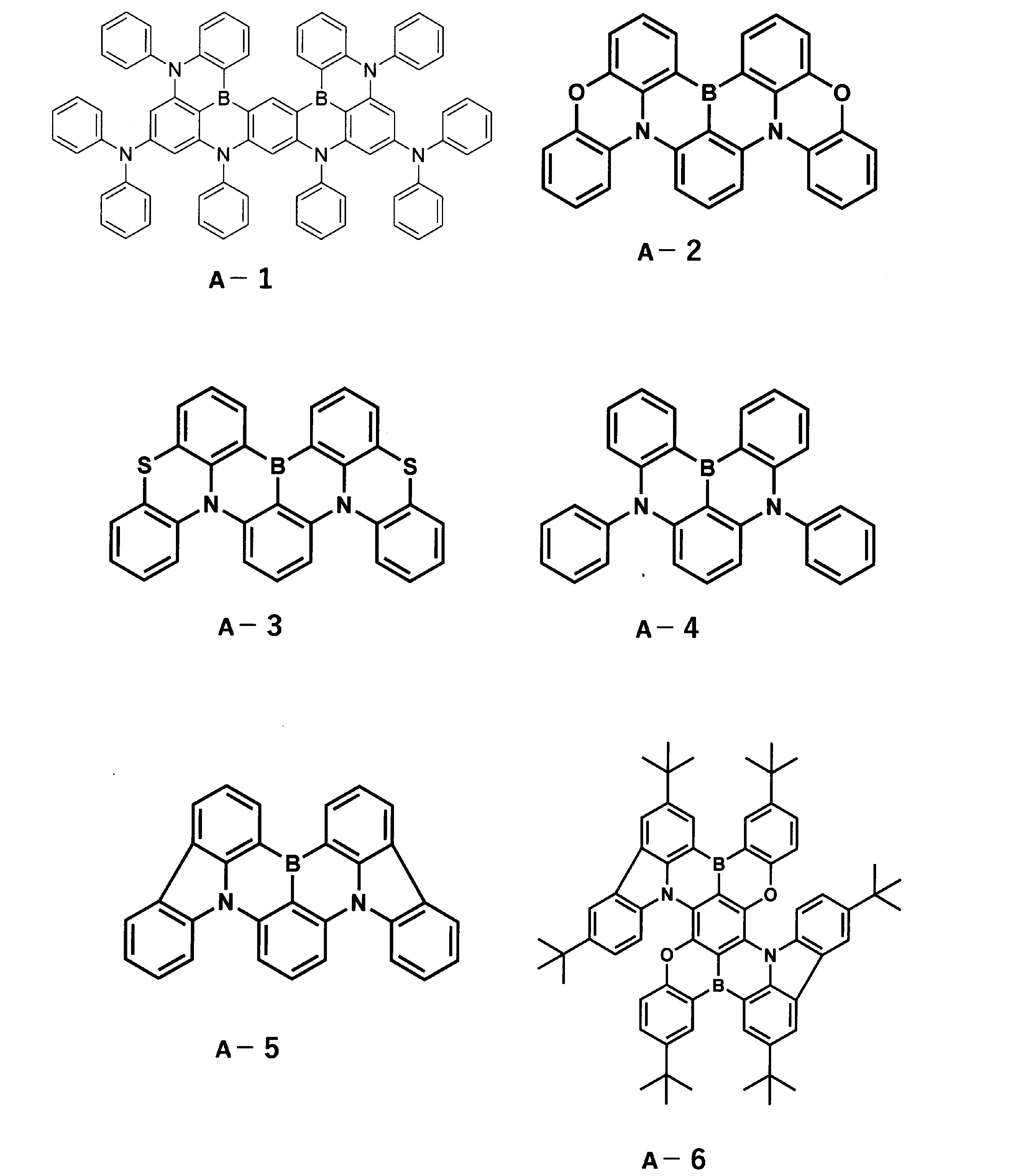
(比較例1)
光電変換層のp型半導体として1,2,3,5-テトラキス(カルバゾール-9-イル)-4,6-ジシアノベンゼン(化合物B-1、膜厚15nm)を用いたこと以外は実施例1と同様にして光センサを得た。
光電変換層のp型半導体として1,2,3,5-テトラキス(カルバゾール-9-イル)-4,6-ジシアノベンゼン(化合物B-1、膜厚15nm)を用いたこと以外は実施例1と同様にして光センサを得た。
(比較例2)
光電変換層のp型半導体としてN,N-ジメチルキナクリドン(化合物B-2、膜厚15nm)を用いたこととアルミニウムの膜厚を26nmに変更したこと以外、比較例1と同様に光センサを得た。
光電変換層のp型半導体としてN,N-ジメチルキナクリドン(化合物B-2、膜厚15nm)を用いたこととアルミニウムの膜厚を26nmに変更したこと以外、比較例1と同様に光センサを得た。
(比較例3)
光電変換層のp型半導体として化合物B-3(膜厚15nm)を用いたこととアルミニウムの膜厚を40nmに変更したこと以外、比較例1と同様に光センサを得た。
光電変換層のp型半導体として化合物B-3(膜厚15nm)を用いたこととアルミニウムの膜厚を40nmに変更したこと以外、比較例1と同様に光センサを得た。
(比較例4)
化合物1で形成される正孔輸送層に対して正孔取り出し層に用いられる、フッ素原子およびシアノ基を構造中に含む化合物4を5%ドープさせたこと、アルミニウムの膜厚を69nmに変更したこと以外、比較例3と同様に光センサを得た。
化合物1で形成される正孔輸送層に対して正孔取り出し層に用いられる、フッ素原子およびシアノ基を構造中に含む化合物4を5%ドープさせたこと、アルミニウムの膜厚を69nmに変更したこと以外、比較例3と同様に光センサを得た。
(比較例5)
光電変換層のp型半導体として化合物B-4(膜厚15nm)を用いたこととアルミニウムの膜厚を80nmに変更したこと以外、比較例1と同様に光センサを得た。
光電変換層のp型半導体として化合物B-4(膜厚15nm)を用いたこととアルミニウムの膜厚を80nmに変更したこと以外、比較例1と同様に光センサを得た。
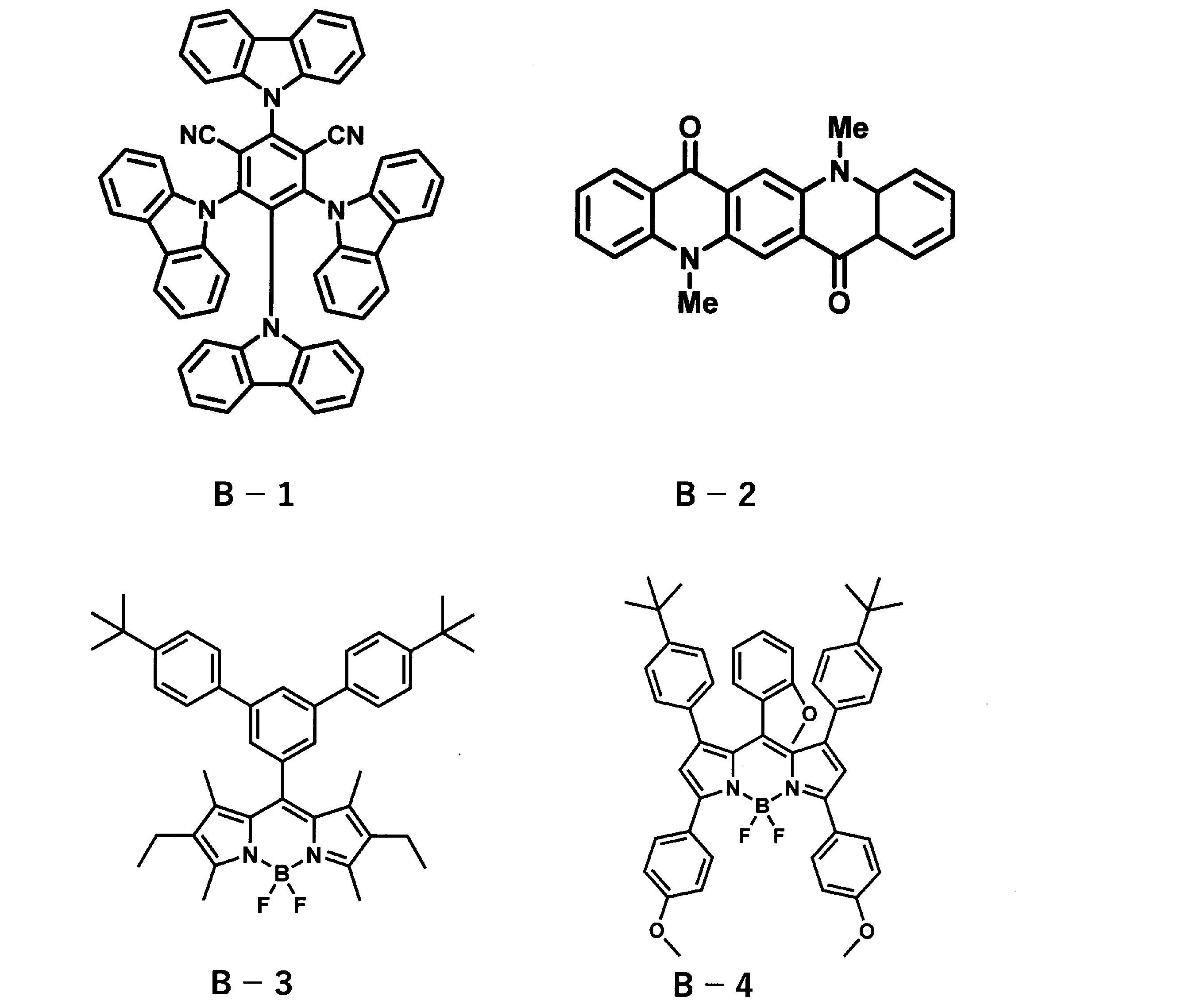
実施例および比較例で得られた光センサを上述の手法に従い測定し、-3V印加時における光センサの極大吸収波長[nm]とその時の光電変換効率およびI-Photo/I-Darkの結果を示す。

実施例1、実施例4、実施例5、実施例8、実施例9では青色光を、実施例2、実施例3、実施例7では緑色光を、実施例6、実施例10では赤色光を吸収し光電変換効果を示していることが分かる。比較例1は青色吸収領域である450nmでの光電変換効率は0%であった。さらに緑色光吸収を示す化合物B-2およびB-3と赤色光吸収を示す化合物B-4を対応する可視光領域を吸収する実施例化合物と比較した場合、実施例化合物の方が、光電変換効率が良好であることが分かる。
I-Photo/I-Darkの比は大きな数値になるほど、光センサとしての感度が高い。実施例7~10と比較例4は正孔輸送層に正孔取り出し層に用いられる一般式(2)で表される、フッ素原子およびシアノ基を構造中に含む化合物4をドープした光センサである。これらのI-Photo/I-Darkを比較した場合、比較例よりも実施例の方が大きな数値を示しており、一般式(1)と一般式(2)で表される化合物を組み合わせることで光センサの感度が向上することが分かる。また、実施例1、実施例3、実施例5および実施例6は実施例7~10に対して一般式(2)で表される化合物を含まずに光電変換素子を作製した結果である。これらを光電変換層中に用いられる一般式(1)で表されるp型半導体別に対応させて比較すると、正孔取り出し層に用いられる一般式(2)で表される化合物を含むことによって、I-Photo/I-Darkの値が大きくなり、光センサの感度が向上することが分かる。また、実施例3および実施例5と実施例7および実施例8を比較すると、一般式(2)で表される化合物を含む素子である実施例7および実施例8において光電変換効率が向上していることが分かる。すなわち、一般式(1)と一般式(2)で表される化合物を組み合わせることで、光電変換効率を向上させることができる。
Claims (13)
- 陽極と陰極の間に光電変換層が存在し、光を電気信号に変換する光センサであって、前記光電変換層が、下記一般式(1)で表される構造を有する化合物、または下記一般式(1)で表される構造を有する多量体を含む、光センサ。

Raは、それぞれ独立に、水素原子、置換もしくは無置換のアルキル基、置換もしくは無置換のシクロアルキル基、置換もしくは無置換の複素環基、置換もしくは無置換のアルケニル基、置換もしくは無置換のシクロアルケニル基、置換もしくは無置換のアルキニル基、置換もしくは無置換のアリール基、置換もしくは無置換のヘテロアリール基、水酸基、チオール基、置換もしくは無置換のアルコキシ基、置換もしくは無置換のアルキルチオ基、置換もしくは無置換のアリールエーテル基、置換もしくは無置換のアリールチオエーテル基、ハロゲン、シアノ基、アルデヒド基、置換もしくは無置換のカルボニル基、置換もしくは無置換のカルボキシル基、置換もしくは無置換のオキシカルボニル基、置換もしくは無置換のエステル基、置換もしくは無置換のカルバモイル基、置換もしくは無置換のアミド基、スルホニル基、置換もしくは無置換のスルホン酸エステル基、置換もしくは無置換のスルホンアミド基、置換もしくは無置換のアミノ基、ニトロ基、置換もしくは無置換のシリル基、置換もしくは無置換のシロキサニル基、置換もしくは無置換のボリル基、置換もしくは無置換のホスフィンオキシド基、置換もしくは無置換のイミノ基、および隣接置換基との間に形成される縮合環および脂肪族環の中から選ばれる。また、Raは、前記置換基でさらに置換されていてもよい。RbはRaと同義である。) - Eがホウ素原子であり、かつZ1およびZ2がそれぞれ独立に酸素原子またはNRaである、請求項1に記載の光センサ。
- 環Za、環Zbおよび環Zcが、それぞれ独立に、置換もしくは無置換の環形成炭素数6~30のアリール環である、請求項1に記載の光センサ。
- Raが置換もしくは無置換のアリール基である、請求項1に記載の光センサ。
- 前記光電変換層が、前記一般式(1)で表される構造を有する化合物として下記一般式(3)または(4)で表される構造を有する化合物を含む、請求項1記載の光センサ。

- 前記光電変換層が、一般式(1)で表される構造を有する多量体を含む、請求項1に記載の光センサ。
- 前記一般式(1)で表される構造を有する多量体が下記一般式(5)、(6)または(7)で表される構造を有する化合物である、請求項6に記載の光センサ。
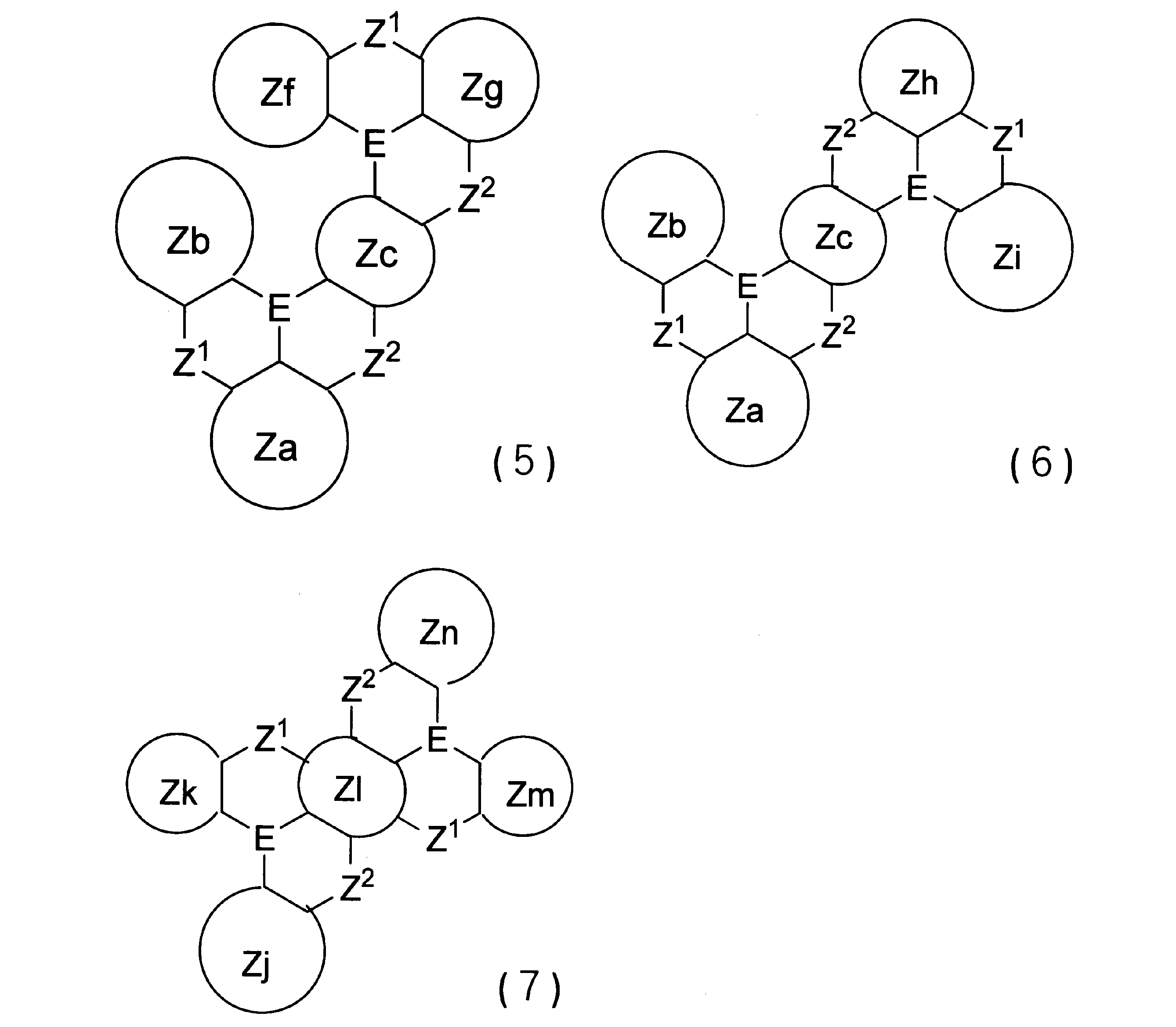
- 前記光電変換層がさらにn型有機半導体を含有する、請求項1に記載の光センサ。
- 前記光電変換層と前記陽極の間に正孔取り出し層を有し、前記正孔取り出し層がハロゲン原子および/またはシアノ基を含有する化合物を含む、請求項1に記載の光センサ。
- 前記ハロゲン原子および/またはシアノ基を含有する化合物が下記一般式(2)で表される化合物である、請求項9に記載の光センサ。

- 請求項1~10のいずれかに記載の光センサと有機発光素子とを有し、前記有機発光素子の光を利用して対象情報を検知する機能を有する、表示装置。
- 前記対象情報が指紋情報である、請求項11に記載の表示装置。
- 前記対象情報が静脈情報である、請求項11に記載の表示装置。
Priority Applications (1)
| Application Number | Priority Date | Filing Date | Title |
|---|---|---|---|
| JP2024508388A JPWO2024166755A1 (ja) | 2023-02-07 | 2024-01-31 |
Applications Claiming Priority (4)
| Application Number | Priority Date | Filing Date | Title |
|---|---|---|---|
| JP2023016561 | 2023-02-07 | ||
| JP2023-016561 | 2023-02-07 | ||
| JP2023133787 | 2023-08-21 | ||
| JP2023-133787 | 2023-08-21 |
Publications (1)
| Publication Number | Publication Date |
|---|---|
| WO2024166755A1 true WO2024166755A1 (ja) | 2024-08-15 |
Family
ID=92262461
Family Applications (1)
| Application Number | Title | Priority Date | Filing Date |
|---|---|---|---|
| PCT/JP2024/002988 Ceased WO2024166755A1 (ja) | 2023-02-07 | 2024-01-31 | 光センサおよびそれを用いた表示装置 |
Country Status (2)
| Country | Link |
|---|---|
| JP (1) | JPWO2024166755A1 (ja) |
| WO (1) | WO2024166755A1 (ja) |
Cited By (1)
| Publication number | Priority date | Publication date | Assignee | Title |
|---|---|---|---|---|
| WO2026048492A1 (ja) * | 2024-08-26 | 2026-03-05 | 日鉄ケミカル&マテリアル株式会社 | 光電変換素子用色素材料及びこれを用いた光電変換素子及びこれを用いたイメージセンサー |
Citations (7)
| Publication number | Priority date | Publication date | Assignee | Title |
|---|---|---|---|---|
| JP2009060051A (ja) * | 2007-09-03 | 2009-03-19 | National Institute Of Advanced Industrial & Technology | 有機太陽電池及び光センサ |
| WO2014156771A1 (ja) * | 2013-03-28 | 2014-10-02 | 新日鉄住金化学株式会社 | 有機薄膜太陽電池 |
| JP2020519002A (ja) * | 2017-03-30 | 2020-06-25 | ノヴァレッド ゲーエムベーハー | 半導体の有機層を形成するためのインク組成物 |
| JP2021014446A (ja) * | 2019-06-07 | 2021-02-12 | 学校法人関西学院 | アミノ置換多環芳香族化合物 |
| KR20220041028A (ko) * | 2020-09-24 | 2022-03-31 | 경상국립대학교산학협력단 | 보론 화합물 및 이를 포함하는 유기 전자 소자 |
| WO2022158425A1 (ja) * | 2021-01-22 | 2022-07-28 | 国立大学法人九州大学 | 有機受光素子及び受光装置 |
| WO2022224893A1 (ja) * | 2021-04-21 | 2022-10-27 | 住友化学株式会社 | インク組成物及びその製造方法 |
-
2024
- 2024-01-31 WO PCT/JP2024/002988 patent/WO2024166755A1/ja not_active Ceased
- 2024-01-31 JP JP2024508388A patent/JPWO2024166755A1/ja active Pending
Patent Citations (7)
| Publication number | Priority date | Publication date | Assignee | Title |
|---|---|---|---|---|
| JP2009060051A (ja) * | 2007-09-03 | 2009-03-19 | National Institute Of Advanced Industrial & Technology | 有機太陽電池及び光センサ |
| WO2014156771A1 (ja) * | 2013-03-28 | 2014-10-02 | 新日鉄住金化学株式会社 | 有機薄膜太陽電池 |
| JP2020519002A (ja) * | 2017-03-30 | 2020-06-25 | ノヴァレッド ゲーエムベーハー | 半導体の有機層を形成するためのインク組成物 |
| JP2021014446A (ja) * | 2019-06-07 | 2021-02-12 | 学校法人関西学院 | アミノ置換多環芳香族化合物 |
| KR20220041028A (ko) * | 2020-09-24 | 2022-03-31 | 경상국립대학교산학협력단 | 보론 화합물 및 이를 포함하는 유기 전자 소자 |
| WO2022158425A1 (ja) * | 2021-01-22 | 2022-07-28 | 国立大学法人九州大学 | 有機受光素子及び受光装置 |
| WO2022224893A1 (ja) * | 2021-04-21 | 2022-10-27 | 住友化学株式会社 | インク組成物及びその製造方法 |
Non-Patent Citations (1)
| Title |
|---|
| XU WANG, DIANLI ZHOU, JIANG HUANG, JUNSHENG YU: "High performance organic ultraviolet photodetector with efficient electroluminescence realized by a thermally activated delayed fluorescence emitter", APPLIED PHYSICS LETTERS, AMERICAN INSTITUTE OF PHYSICS, 2 HUNTINGTON QUADRANGLE, MELVILLE, NY 11747, vol. 107, no. 4, 27 July 2015 (2015-07-27), 2 Huntington Quadrangle, Melville, NY 11747, pages 043303, XP055381692, ISSN: 0003-6951, DOI: 10.1063/1.4927652 * |
Cited By (1)
| Publication number | Priority date | Publication date | Assignee | Title |
|---|---|---|---|---|
| WO2026048492A1 (ja) * | 2024-08-26 | 2026-03-05 | 日鉄ケミカル&マテリアル株式会社 | 光電変換素子用色素材料及びこれを用いた光電変換素子及びこれを用いたイメージセンサー |
Also Published As
| Publication number | Publication date |
|---|---|
| JPWO2024166755A1 (ja) | 2024-08-15 |
Similar Documents
| Publication | Publication Date | Title |
|---|---|---|
| EP2799515B1 (en) | Compound for organic optoelectric device, organic light-emitting diode including same, and display device including organic light-emitting diode | |
| EP2860783B1 (en) | Organic optoelectric device and display device | |
| EP3042943B1 (en) | Composition for organic optoelectronic device, organic optoelectronic device, and display device | |
| KR102233924B1 (ko) | 광전자 부품들을 위한 광활성 유기 재료 | |
| CN106575708B (zh) | 光电转换元件以及使用其的图像传感器、太阳能电池、单色检测传感器及柔性传感器 | |
| KR102480671B1 (ko) | 광전 변환 소자 및 이미지 센서 | |
| JP5988001B1 (ja) | 光電変換素子およびこれを用いたイメージセンサ | |
| WO2024007511A1 (zh) | 芳胺化合物及有机电致发光器件和电子装置 | |
| WO2015115744A1 (ko) | 전자수송보조층용 조성물, 전자수송보조층을 포함하는 유기 광전자 소자 및 표시 장치 | |
| CN115804259A (zh) | 光电转换元件及其制造方法 | |
| CN114181166A (zh) | 有机化合物及包含其的电子元件和电子装置 | |
| CN113121408A (zh) | 含氮化合物、电子元件和电子装置 | |
| CN105980300B (zh) | 富勒烯衍生物、使用其的有机太阳能电池及其制造方法 | |
| JP7771655B2 (ja) | 光電変換材料およびそれを用いた光電変換素子 | |
| KR102056515B1 (ko) | 조성물 및 이를 포함하는 유기전자소자 | |
| JP2024107708A (ja) | 光センサ材料、およびそれを用いた光センサ | |
| JP2025011041A (ja) | 電子ドナー型光電変換材料、それを用いた光電変換素子、光センサおよび表示装置 | |
| JP2016072547A (ja) | 光電変換素子およびこれを用いたイメージセンサ | |
| WO2023176829A1 (ja) | 光起電力素子、光センサ、撮像素子および指紋認証装置 | |
| WO2024162088A1 (ja) | 光センサ、それを用いた表示装置、化合物 | |
| JP2024168884A (ja) | 電子ドナー型光電変換材料、それを用いた光電変換素子、光センサおよび表示装置ならびに化合物。 | |
| WO2025013627A1 (ja) | 光電変換材料ならびにそれを用いた光電変換素子、光センサおよび表示装置 | |
| KR20250005970A (ko) | 광 센서 및 이것을 사용한 표시 장치 | |
| WO2024210055A1 (ja) | 光電変換材料ならびにそれを用いた光電変換素子、光センサ、表示装置および化合物 | |
| CN118575605A (zh) | 光传感器及使用其的显示装置 |
Legal Events
| Date | Code | Title | Description |
|---|---|---|---|
| WWE | Wipo information: entry into national phase |
Ref document number: 2024508388 Country of ref document: JP |
|
| 121 | Ep: the epo has been informed by wipo that ep was designated in this application |
Ref document number: 24753199 Country of ref document: EP Kind code of ref document: A1 |
|
| NENP | Non-entry into the national phase |
Ref country code: DE |
|
| 122 | Ep: pct application non-entry in european phase |
Ref document number: 24753199 Country of ref document: EP Kind code of ref document: A1 |