WO2024166561A1 - 駆動回路、信号伝達装置、電子機器、車両 - Google Patents
駆動回路、信号伝達装置、電子機器、車両 Download PDFInfo
- Publication number
- WO2024166561A1 WO2024166561A1 PCT/JP2023/046196 JP2023046196W WO2024166561A1 WO 2024166561 A1 WO2024166561 A1 WO 2024166561A1 JP 2023046196 W JP2023046196 W JP 2023046196W WO 2024166561 A1 WO2024166561 A1 WO 2024166561A1
- Authority
- WO
- WIPO (PCT)
- Prior art keywords
- potential
- chip
- insulating layer
- transformer
- coil
- Prior art date
- Legal status (The legal status is an assumption and is not a legal conclusion. Google has not performed a legal analysis and makes no representation as to the accuracy of the status listed.)
- Ceased
Links
Images


Classifications
-
- H—ELECTRICITY
- H03—ELECTRONIC CIRCUITRY
- H03K—PULSE TECHNIQUE
- H03K17/00—Electronic switching or gating, i.e. not by contact-making and –breaking
- H03K17/51—Electronic switching or gating, i.e. not by contact-making and –breaking characterised by the components used
- H03K17/56—Electronic switching or gating, i.e. not by contact-making and –breaking characterised by the components used by the use, as active elements, of semiconductor devices
-
- H—ELECTRICITY
- H02—GENERATION; CONVERSION OR DISTRIBUTION OF ELECTRIC POWER
- H02H—EMERGENCY PROTECTIVE CIRCUIT ARRANGEMENTS
- H02H3/00—Emergency protective circuit arrangements for automatic disconnection directly responsive to an undesired change from normal electric working condition with or without subsequent reconnection ; integrated protection
- H02H3/08—Emergency protective circuit arrangements for automatic disconnection directly responsive to an undesired change from normal electric working condition with or without subsequent reconnection ; integrated protection responsive to excess current
-
- H—ELECTRICITY
- H02—GENERATION; CONVERSION OR DISTRIBUTION OF ELECTRIC POWER
- H02M—APPARATUS FOR CONVERSION BETWEEN AC AND AC, BETWEEN AC AND DC, OR BETWEEN DC AND DC, AND FOR USE WITH MAINS OR SIMILAR POWER SUPPLY SYSTEMS; CONVERSION OF DC OR AC INPUT POWER INTO SURGE OUTPUT POWER; CONTROL OR REGULATION THEREOF
- H02M1/00—Details of apparatus for conversion
- H02M1/08—Circuits specially adapted for the generation of control voltages for semiconductor devices incorporated in static converters
-
- H—ELECTRICITY
- H02—GENERATION; CONVERSION OR DISTRIBUTION OF ELECTRIC POWER
- H02M—APPARATUS FOR CONVERSION BETWEEN AC AND AC, BETWEEN AC AND DC, OR BETWEEN DC AND DC, AND FOR USE WITH MAINS OR SIMILAR POWER SUPPLY SYSTEMS; CONVERSION OF DC OR AC INPUT POWER INTO SURGE OUTPUT POWER; CONTROL OR REGULATION THEREOF
- H02M7/00—Conversion of AC power input into DC power output; Conversion of DC power input into AC power output
- H02M7/42—Conversion of DC power input into AC power output without possibility of reversal
- H02M7/44—Conversion of DC power input into AC power output without possibility of reversal by static converters
- H02M7/48—Conversion of DC power input into AC power output without possibility of reversal by static converters using discharge tubes with control electrode or semiconductor devices with control electrode
-
- H—ELECTRICITY
- H03—ELECTRONIC CIRCUITRY
- H03K—PULSE TECHNIQUE
- H03K17/00—Electronic switching or gating, i.e. not by contact-making and –breaking
- H03K17/51—Electronic switching or gating, i.e. not by contact-making and –breaking characterised by the components used
- H03K17/56—Electronic switching or gating, i.e. not by contact-making and –breaking characterised by the components used by the use, as active elements, of semiconductor devices
- H03K17/567—Circuits characterised by the use of more than one type of semiconductor device, e.g. BIMOS, composite devices such as IGBT
-
- H—ELECTRICITY
- H10—SEMICONDUCTOR DEVICES; ELECTRIC SOLID-STATE DEVICES NOT OTHERWISE PROVIDED FOR
- H10D—INORGANIC ELECTRIC SEMICONDUCTOR DEVICES
- H10D30/00—Field-effect transistors [FET]
- H10D30/60—Insulated-gate field-effect transistors [IGFET]
-
- H—ELECTRICITY
- H10—SEMICONDUCTOR DEVICES; ELECTRIC SOLID-STATE DEVICES NOT OTHERWISE PROVIDED FOR
- H10D—INORGANIC ELECTRIC SEMICONDUCTOR DEVICES
- H10D84/00—Integrated devices formed in or on semiconductor substrates that comprise only semiconducting layers, e.g. on Si wafers or on GaAs-on-Si wafers
- H10D84/01—Manufacture or treatment
- H10D84/02—Manufacture or treatment characterised by using material-based technologies
- H10D84/03—Manufacture or treatment characterised by using material-based technologies using Group IV technology, e.g. silicon technology or silicon-carbide [SiC] technology
- H10D84/038—Manufacture or treatment characterised by using material-based technologies using Group IV technology, e.g. silicon technology or silicon-carbide [SiC] technology using silicon technology, e.g. SiGe
Definitions
- This disclosure relates to a drive circuit, a signal transmission device, an electronic device, and a vehicle.
- Patent Document 1 As an example of related prior art, see Patent Document 1 by the same applicant.
- the drive circuit disclosed in this specification includes a short circuit detection circuit configured to detect a short circuit state in which an excessive short circuit current may flow through a switch element, and a controller configured to forcibly turn off the switch element when the short circuit state is detected, and when forcibly turning off the switch element, the controller switches an output pulse signal for driving the switch element from an on logic level to an off logic level while gradually lowering the slew rate.
- This disclosure makes it possible to provide a drive circuit that can suppress voltage surges and reduce losses by using soft turn-off control when a short circuit is detected, as well as a signal transmission device, electronic device, and vehicle that use the same.
- FIG. 1 is a diagram showing a basic configuration of a signal transmission device.
- FIG. 2 is a diagram showing the basic structure of a transformer chip.
- FIG. 3 is a perspective view of a semiconductor device used as a two-channel type transformer chip.
- FIG. 4 is a plan view of the semiconductor device shown in FIG.
- FIG. 5 is a plan view showing a layer in which the low potential coil is formed in the semiconductor device of FIG.
- FIG. 6 is a plan view showing a layer in which a high potential coil is formed in the semiconductor device of FIG.
- FIG. 7 is a cross-sectional view taken along line VIII-VIII shown in FIG.
- FIG. 8 is an enlarged view (isolation structure) of the region XIII shown in FIG.
- FIG. 9 is a diagram illustrating an example of the layout of a transformer chip.
- FIG. 10 is a diagram showing a first embodiment of a signal transmission device.
- FIG. 11 is a diagram illustrating an example of a short circuit detection operation in the first embodiment.
- FIG. 12 is a diagram showing a second embodiment of a signal transmission device.
- FIG. 13 is a diagram illustrating an example of a short circuit detection operation in the second embodiment.
- FIG. 14 is a diagram showing the external appearance of the vehicle.
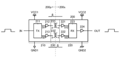
- ⁇ Signal transmission device (basic configuration)> 1 is a diagram showing the basic configuration of a signal transmission device.
- the signal transmission device 200 of this configuration example is a semiconductor integrated circuit device (so-called insulated gate driver IC) that transmits a pulse signal from the primary circuit system 200p to the secondary circuit system 200s while isolating the primary circuit system 200p (VCC1-GND1 system) from the secondary circuit system 200s (VCC2-GND2 system) and drives the gate of a switch element (not shown) provided in the secondary circuit system 200s.
- the signal transmission device 200 is formed by sealing a controller chip 210, a driver chip 220, and a transformer chip 230 in a single package.
- the controller chip 210 is a semiconductor chip that operates by receiving a power supply voltage VCC1 (for example, up to 7 V based on GND1).
- the controller chip 210 includes, for example, a pulse transmission circuit 211 and buffers 212 and 213 integrated therein.
- the pulse transmission circuit 211 is a pulse generator that generates the transmission pulse signals S11 and S21 in response to the input pulse signal IN. More specifically, when the pulse transmission circuit 211 notifies that the input pulse signal IN is at a high level, it pulse drives the transmission pulse signal S11 (outputs a single or multiple transmission pulses), and when it notifies that the input pulse signal IN is at a low level, it pulse drives the transmission pulse signal S21. In other words, the pulse transmission circuit 211 pulse drives either the transmission pulse signal S11 or S21 in response to the logical level of the input pulse signal IN.
- the buffer 212 receives the transmission pulse signal S11 from the pulse transmission circuit 211 and pulse-drives the transformer chip 230 (specifically, the transformer 231).
- the buffer 213 receives the transmission pulse signal S21 from the pulse transmission circuit 211 and pulse-drives the transformer chip 230 (specifically, the transformer 232).
- the driver chip 220 is a semiconductor chip that operates by receiving a power supply voltage VCC2 (for example, up to 30 V based on GND2).
- the driver chip 220 includes, for example, buffers 221 and 222, a pulse receiving circuit 223, and a driver 224.
- the buffer 221 shapes the waveform of the received pulse signal S12 induced in the transformer chip 230 (specifically, the transformer 231) and outputs it to the pulse receiving circuit 223.
- the buffer 222 shapes the waveform of the received pulse signal S22 induced in the transformer chip 230 (specifically, the transformer 232) and outputs it to the pulse receiving circuit 223.
- the pulse receiving circuit 223 generates the output pulse signal OUT by driving the driver 224 in response to the received pulse signals S12 and S22 input via the buffers 221 and 222. More specifically, the pulse receiving circuit 223 drives the driver 224 so as to raise the output pulse signal OUT to a high level in response to the pulse drive of the received pulse signal S12, and to lower the output pulse signal OUT to a low level in response to the pulse drive of the received pulse signal S22. In other words, the pulse receiving circuit 223 switches the logical level of the output pulse signal OUT in response to the logical level of the input pulse signal IN.
- an RS flip-flop can be suitably used as the pulse receiving circuit 223.
- the driver 224 generates an output pulse signal OUT based on the drive control of the pulse receiving circuit 223.
- the transformer chip 230 uses transformers 231 and 232 to provide DC insulation between the controller chip 210 and the driver chip 220, and outputs the transmission pulse signals S11 and S21 input from the pulse transmission circuit 211 to the pulse reception circuit 223 as reception pulse signals S12 and S22, respectively.
- DC insulation means that the objects to be insulated are not connected by a conductor.
- the transformer 231 outputs a received pulse signal S12 from the secondary coil 231s in response to a transmitted pulse signal S11 input to the primary coil 231p.
- the transformer 232 outputs a received pulse signal S22 from the secondary coil 232s in response to a transmitted pulse signal S21 input to the primary coil 232p.
- the input pulse signal IN is separated into two transmission pulse signals S11 and S21 (corresponding to the rise signal and fall signal), and then transmitted from the primary circuit system 200p to the secondary circuit system 200s via the two transformers 231 and 232.
- the signal transmission device 200 of this configuration example has an independent transformer chip 230 equipped with only transformers 231 and 232, separate from the controller chip 210 and driver chip 220, and these three chips are sealed in a single package.
- the controller chip 210 and the driver chip 220 can both be formed using a general low to medium voltage process (withstands a few volts to several tens of volts), eliminating the need to use a dedicated high voltage process (withstands a few kV), making it possible to reduce manufacturing costs.
- the signal transmission device 200 can be suitably used, for example, in a power supply device or a motor drive device for on-board equipment mounted in a vehicle.
- the above vehicles include not only engine vehicles, but also electric vehicles (BEVs [battery electric vehicles], HEVs [hybrid electric vehicles], PHEVs/PHVs (plug-in hybrid electric vehicles/plug-in hybrid vehicles), or xEVs such as FCEVs/FCVs (fuel cell electric vehicles/fuel cell vehicles)).
- FIG. 2 is a diagram showing the basic structure of the transformer chip 230.
- the transformer 231 includes a primary coil 231p and a secondary coil 231s that face each other in the vertical direction.
- the transformer 232 includes a primary coil 232p and a secondary coil 232s that face each other in the vertical direction.
- the primary coils 231p and 232p are both formed on the first wiring layer (lower layer) 230a of the transformer chip 230.
- the secondary coils 231s and 232s are both formed on the second wiring layer (upper layer in this figure) 230b of the transformer chip 230.
- the secondary coil 231s is disposed directly above the primary coil 231p and faces the primary coil 231p.
- the secondary coil 232s is disposed directly above the primary coil 232p and faces the primary coil 232p.
- the primary coil 231p is laid in a spiral shape starting from a first end connected to the internal terminal X21, surrounding the internal terminal X21 in a clockwise direction, and its second end corresponding to its end point is connected to the internal terminal X22.
- the primary coil 232p is laid in a spiral shape starting from a first end connected to the internal terminal X23, surrounding the internal terminal X23 in a counterclockwise direction, and its second end corresponding to its end point is connected to the internal terminal X22.
- the internal terminals X21, X22, and X23 are linearly arranged in the order shown.
- the internal terminal X21 is connected to the external terminal T21 of the second layer 230b via the conductive wiring Y21 and via Z21.
- the internal terminal X22 is connected to the external terminal T22 of the second layer 230b via the conductive wiring Y22 and via Z22.
- the internal terminal X23 is connected to the external terminal T23 of the second layer 230b via the conductive wiring Y23 and via Z23.
- the external terminals T21 to T23 are arranged in a straight line and are used for wire bonding with the controller chip 210.
- the secondary coil 231s is laid in a spiral shape starting from a first end connected to the external terminal T24, surrounding the external terminal T24 in a counterclockwise direction, and its second end corresponding to its end point is connected to the external terminal T25.
- the secondary coil 232s is laid in a spiral shape starting from a first end connected to the external terminal T26, surrounding the external terminal T26 in a clockwise direction, and its second end corresponding to its end point is connected to the external terminal T25.
- the external terminals T24, T25, and T26 are arranged linearly in the order shown in the figure, and are used for wire bonding with the driver chip 220.
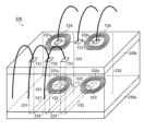
- FIG. 3 is a perspective view showing a semiconductor device 5 used as a two-channel type transformer chip.
- FIG. 4 is a plan view of the semiconductor device 5 shown in FIG. 3.
- FIG. 5 is a plan view showing a layer in which a low potential coil 22 (corresponding to a primary coil of a transformer) is formed in the semiconductor device 5 shown in FIG. 3.
- FIG. 6 is a plan view showing a layer in which a high potential coil 23 (corresponding to a secondary coil of a transformer) is formed in the semiconductor device 5 shown in FIG. 3.
- FIG. 7 is a cross-sectional view taken along line VIII-VIII shown in FIG. 6.
- FIG. 8 is an enlarged view of region XIII shown in FIG. 7, showing an isolation structure 130.
- the semiconductor device 5 includes a semiconductor chip 41 having a rectangular parallelepiped shape.
- the semiconductor chip 41 includes at least one of silicon, a wide band gap semiconductor, and a compound semiconductor.
- a wide bandgap semiconductor is made of a semiconductor whose bandgap exceeds that of silicon (approximately 1.12 eV).
- the bandgap of a wide bandgap semiconductor is preferably 2.0 eV or more.
- the wide bandgap semiconductor may be SiC (silicon carbide).
- the compound semiconductor may be a III-V compound semiconductor.
- the compound semiconductor may include at least one of AlN (aluminum nitride), InN (indium nitride), GaN (gallium nitride), and GaAs (gallium arsenide).
- the semiconductor chip 41 includes a semiconductor substrate made of silicon.
- the semiconductor chip 41 may be an epitaxial substrate having a layered structure including a semiconductor substrate made of silicon and an epitaxial layer made of silicon.
- the conductivity type of the semiconductor substrate may be n-type or p-type.
- the epitaxial layer may be n-type or p-type.
- the semiconductor chip 41 has a first main surface 42 on one side, a second main surface 43 on the other side, and chip sidewalls 44A-44D connecting the first main surface 42 and the second main surface 43.
- the first main surface 42 and the second main surface 43 are formed in a quadrangular shape (rectangular in this embodiment) when viewed in a plan view from their normal direction Z (hereinafter simply referred to as "plan view").
- the chip sidewalls 44A to 44D include a first chip sidewall 44A, a second chip sidewall 44B, a third chip sidewall 44C, and a fourth chip sidewall 44D.
- the first chip sidewall 44A and the second chip sidewall 44B form the long sides of the semiconductor chip 41.
- the first chip sidewall 44A and the second chip sidewall 44B extend along the first direction X and face the second direction Y.
- the third chip sidewall 44C and the fourth chip sidewall 44D form the short sides of the semiconductor chip 41.
- the third chip sidewall 44C and the fourth chip sidewall 44D extend in the second direction Y and face the first direction X.
- the chip sidewalls 44A to 44D are made of ground surfaces.
- the semiconductor device 5 further includes an insulating layer 51 formed on the first main surface 42 of the semiconductor chip 41.
- the insulating layer 51 has an insulating main surface 52 and insulating side walls 53A-53D.
- the insulating main surface 52 is formed in a quadrangular shape (rectangular in this embodiment) that matches the first main surface 42 in a plan view.
- the insulating main surface 52 extends parallel to the first main surface 42.
- the insulating sidewalls 53A to 53D include a first insulating sidewall 53A, a second insulating sidewall 53B, a third insulating sidewall 53C, and a fourth insulating sidewall 53D.
- the insulating sidewalls 53A to 53D extend from the periphery of the insulating main surface 52 toward the semiconductor chip 41 and are continuous with the chip sidewalls 44A to 44D. Specifically, the insulating sidewalls 53A to 53D are formed flush with the chip sidewalls 44A to 44D.
- the insulating sidewalls 53A to 53D form a ground surface that is flush with the chip sidewalls 44A to 44D.
- the insulating layer 51 is made of a multi-layer insulating laminate structure including a bottom insulating layer 55, a top insulating layer 56, and a plurality of (11 in this embodiment) interlayer insulating layers 57.
- the bottom insulating layer 55 is an insulating layer that directly covers the first main surface 42.
- the top insulating layer 56 is an insulating layer that forms the insulating main surface 52.
- the plurality of interlayer insulating layers 57 are insulating layers interposed between the bottom insulating layer 55 and the top insulating layer 56.
- the bottom insulating layer 55 has a single-layer structure including silicon oxide.
- the top insulating layer 56 has a single-layer structure including silicon oxide.
- the thickness of the bottom insulating layer 55 and the top insulating layer 56 may each be 1 ⁇ m or more and 3 ⁇ m or less (for example, about 2 ⁇ m).
- the multiple interlayer insulating layers 57 each have a stacked structure including a first insulating layer 58 on the bottom insulating layer 55 side and a second insulating layer 59 on the top insulating layer 56 side.
- the first insulating layer 58 may include silicon nitride.
- the first insulating layer 58 is formed as an etching stopper layer for the second insulating layer 59.
- the thickness of the first insulating layer 58 may be 0.1 ⁇ m or more and 1 ⁇ m or less (for example, about 0.3 ⁇ m).
- the second insulating layer 59 is formed on the first insulating layer 58. It contains an insulating material different from that of the first insulating layer 58.
- the second insulating layer 59 may contain silicon oxide.
- the thickness of the second insulating layer 59 may be 1 ⁇ m or more and 3 ⁇ m or less (for example, about 2 ⁇ m). It is preferable that the thickness of the second insulating layer 59 exceeds the thickness of the first insulating layer 58.
- the total thickness DT of the insulating layers 51 may be 5 ⁇ m or more and 50 ⁇ m or less.
- the total thickness DT of the insulating layers 51 and the number of layers of the interlayer insulating layers 57 are arbitrary and are adjusted according to the dielectric strength voltage (dielectric breakdown resistance) to be achieved.
- the insulating materials of the bottom insulating layer 55, the top insulating layer 56 and the interlayer insulating layer 57 are arbitrary and are not limited to a specific insulating material.
- the semiconductor device 5 includes a first functional device 45 formed in an insulating layer 51.
- the first functional device 45 includes one or more (in this embodiment, multiple) transformers 21 (corresponding to the aforementioned transformer).
- the semiconductor device 5 is a multi-channel device including multiple transformers 21.
- the multiple transformers 21 are formed in the inner part of the insulating layer 51 at intervals from the insulating side walls 53A-53D.
- the multiple transformers 21 are formed at intervals in the first direction X.
- the multiple transformers 21 specifically include a first transformer 21A, a second transformer 21B, a third transformer 21C, and a fourth transformer 21D, which are formed in this order from the insulating side wall 53C side to the insulating side wall 53D side in a plan view.
- the multiple transformers 21A to 21D each have a similar structure.
- the structure of the first transformer 21A will be explained as an example.
- the explanation of the structures of the second transformer 21B, third transformer 21C, and fourth transformer 21D will be omitted, as the explanation of the structure of the first transformer 21A applies mutatis mutandis.
- the first transformer 21A includes a low-potential coil 22 and a high-potential coil 23.
- the low-potential coil 22 is formed in an insulating layer 51.
- the high-potential coil 23 is formed in the insulating layer 51 so as to face the low-potential coil 22 in the normal direction Z.
- the low-potential coil 22 and the high-potential coil 23 are formed in a region sandwiched between the bottom insulating layer 55 and the top insulating layer 56 (i.e., multiple interlayer insulating layers 57).
- the low-potential coil 22 is formed on the bottom insulating layer 55 (semiconductor chip 41) side within the insulating layer 51, and the high-potential coil 23 is formed on the top insulating layer 56 (insulating main surface 52) side of the low-potential coil 22 within the insulating layer 51.
- the high-potential coil 23 faces the semiconductor chip 41 with the low-potential coil 22 in between.
- the low-potential coil 22 and the high-potential coil 23 may be positioned at any location. Furthermore, it is sufficient that the high-potential coil 23 faces the low-potential coil 22 with one or more interlayer insulating layers 57 in between.
- the distance between the low potential coil 22 and the high potential coil 23 (i.e., the number of layers of the interlayer insulating layer 57) is adjusted appropriately according to the dielectric strength and electric field strength between the low potential coil 22 and the high potential coil 23.
- the low potential coil 22 is formed in the third interlayer insulating layer 57 counting from the bottom insulating layer 55 side.
- the high potential coil 23 is formed in the first interlayer insulating layer 57 counting from the top insulating layer 56 side.
- the low-potential coil 22 is embedded in the interlayer insulating layer 57, penetrating the first insulating layer 58 and the second insulating layer 59.
- the low-potential coil 22 includes a first inner end 24, a first outer end 25, and a first spiral portion 26 wound in a spiral shape between the first inner end 24 and the first outer end 25.
- the first spiral portion 26 is wound in a spiral shape that extends in an elliptical shape (oval shape) in a plan view.
- the portion that forms the innermost periphery of the first spiral portion 26 defines a first inner region 66 that is elliptical in a plan view.
- the number of turns of the first spiral portion 26 may be 5 or more and 30 or less.
- the width of the first spiral portion 26 may be 0.1 ⁇ m or more and 5 ⁇ m or less.
- the width of the first spiral portion 26 is preferably 1 ⁇ m or more and 3 ⁇ m or less.
- the width of the first spiral portion 26 is defined by the width in a direction perpendicular to the spiral direction.
- the first winding pitch of the first spiral portion 26 may be 0.1 ⁇ m or more and 5 ⁇ m or less.
- the first winding pitch is preferably 1 ⁇ m or more and 3 ⁇ m or less.
- the first winding pitch is defined by the distance between two adjacent portions of the first spiral portion 26 in a direction perpendicular to the spiral direction.
- the winding shape of the first spiral portion 26 and the planar shape of the first inner region 66 are arbitrary and are not limited to the form shown in FIG. 5, etc.
- the first spiral portion 26 may be wound in a polygonal shape, such as a triangular shape or a rectangular shape, or in a circular shape in a planar view.
- the first inner region 66 may be partitioned into a polygonal shape, such as a triangular shape or a rectangular shape, or in a circular shape in a planar view, depending on the winding shape of the first spiral portion 26.
- the low potential coil 22 may include at least one of titanium, titanium nitride, copper, aluminum, and tungsten.
- the low potential coil 22 may have a laminated structure including a barrier layer and a main body layer.
- the barrier layer defines a recess space in the interlayer insulating layer 57.
- the barrier layer may include at least one of titanium and titanium nitride.
- the main body layer may include at least one of copper, aluminum, and tungsten.
- the high-potential coil 23 is embedded in the interlayer insulating layer 57, penetrating the first insulating layer 58 and the second insulating layer 59.
- the high-potential coil 23 includes a second inner end 27, a second outer end 28, and a second spiral portion 29 wound in a spiral shape between the second inner end 27 and the second outer end 28.
- the second spiral portion 29 is wound in a spiral shape extending in an elliptical shape (oval shape) in a planar view.
- the portion forming the innermost periphery of the second spiral portion 29 defines a second inner region 67 that is elliptical in a planar view.
- the second inner region 67 of the second spiral portion 29 faces the first inner region 66 of the first spiral portion 26 in the normal direction Z.
- the number of turns of the second spiral portion 29 may be 5 or more and 30 or less.
- the number of turns of the second spiral portion 29 relative to the number of turns of the first spiral portion 26 is adjusted according to the voltage value to be boosted. It is preferable that the number of turns of the second spiral portion 29 exceeds the number of turns of the first spiral portion 26.
- the number of turns of the second spiral portion 29 may be less than the number of turns of the first spiral portion 26, or may be equal to the number of turns of the first spiral portion 26.
- the width of the second spiral portion 29 may be 0.1 ⁇ m or more and 5 ⁇ m or less.
- the width of the second spiral portion 29 is preferably 1 ⁇ m or more and 3 ⁇ m or less.
- the width of the second spiral portion 29 is defined by the width in a direction perpendicular to the spiral direction.
- the width of the second spiral portion 29 is preferably equal to the width of the first spiral portion 26.
- the second winding pitch of the second spiral portion 29 may be 0.1 ⁇ m or more and 5 ⁇ m or less.
- the second winding pitch is preferably 1 ⁇ m or more and 3 ⁇ m or less.
- the second winding pitch is defined by the distance between two adjacent portions of the second spiral portion 29 in a direction perpendicular to the spiral direction.
- the second winding pitch is preferably equal to the first winding pitch of the first spiral portion 26.
- the winding shape of the second spiral portion 29 and the planar shape of the second inner region 67 are arbitrary and are not limited to the form shown in FIG. 6, etc.
- the second spiral portion 29 may be wound in a polygonal shape, such as a triangular shape or a rectangular shape, or in a circular shape in a planar view.
- the second inner region 67 may be partitioned into a polygonal shape, such as a triangular shape or a rectangular shape, or in a circular shape in a planar view, depending on the winding shape of the second spiral portion 29.
- the high-potential coil 23 is preferably formed from the same conductive material as the low-potential coil 22.
- the high-potential coil 23 preferably includes a barrier layer and a main body layer, similar to the low-potential coil 22.
- the semiconductor device 5 includes a plurality of (12 in this figure) low potential terminals 11 and a plurality of (12 in this figure) high potential terminals 12.
- the plurality of low potential terminals 11 are each electrically connected to the low potential coils 22 of the corresponding transformers 21A to 21D.
- the plurality of high potential terminals 12 are each electrically connected to the high potential coils 23 of the corresponding transformers 21A to 21D.
- the low-potential terminals 11 are formed on the insulating main surface 52 of the insulating layer 51. Specifically, the low-potential terminals 11 are formed in an area on the insulating sidewall 53B side at intervals in the second direction Y from the transformers 21A-21D, and are arranged at intervals in the first direction X.
- the low potential terminals 11 include a first low potential terminal 11A, a second low potential terminal 11B, a third low potential terminal 11C, a fourth low potential terminal 11D, a fifth low potential terminal 11E, and a sixth low potential terminal 11F.
- two of each of the low potential terminals 11A to 11F are formed.
- the number of low potential terminals 11A to 11F is arbitrary.
- the first low potential terminal 11A faces the first transformer 21A in the second direction Y in a plan view.
- the second low potential terminal 11B faces the second transformer 21B in the second direction Y in a plan view.
- the third low potential terminal 11C faces the third transformer 21C in the second direction Y in a plan view.
- the fourth low potential terminal 11D faces the fourth transformer 21D in the second direction Y in a plan view.
- the fifth low potential terminal 11E is formed in the area between the first low potential terminal 11A and the second low potential terminal 11B in a plan view.
- the sixth low potential terminal 11F is formed in the area between the third low potential terminal 11C and the fourth low potential terminal 11D in a plan view.
- the first low potential terminal 11A is electrically connected to the first inner end 24 of the first transformer 21A (low potential coil 22).
- the second low potential terminal 11B is electrically connected to the first inner end 24 of the second transformer 21B (low potential coil 22).
- the third low potential terminal 11C is electrically connected to the first inner end 24 of the third transformer 21C (low potential coil 22).
- the fourth low potential terminal 11D is electrically connected to the first inner end 24 of the fourth transformer 21D (low potential coil 22).
- the fifth low potential terminal 11E is electrically connected to the first outer end 25 of the first transformer 21A (low potential coil 22) and the first outer end 25 of the second transformer 21B (low potential coil 22).
- the sixth low potential terminal 11F is electrically connected to the first outer end 25 of the third transformer 21C (low potential coil 22) and the first outer end 25 of the fourth transformer 21D (low potential coil 22).
- the multiple high potential terminals 12 are formed on the insulating main surface 52 of the insulating layer 51 at intervals from the multiple low potential terminals 11. Specifically, the multiple high potential terminals 12 are formed in the area on the insulating side wall 53A side at intervals from the multiple low potential terminals 11 in the second direction Y, and are arranged at intervals in the first direction X.
- the multiple high potential terminals 12 are each formed in an area close to the corresponding transformer 21A-21D in a planar view.
- the high potential terminals 12 being close to the transformers 21A-21D means that the distance between the high potential terminal 12 and the transformer 21 in a planar view is less than the distance between the low potential terminal 11 and the high potential terminal 12.
- the multiple high potential terminals 12 are formed at intervals along the first direction X so as to face the multiple transformers 21A to 21D along the first direction X in a plan view. More specifically, the multiple high potential terminals 12 are formed at intervals along the first direction X so as to be located in the second inner region 67 of the high potential coil 23 and in the region between adjacent high potential coils 23 in a plan view. As a result, the multiple high potential terminals 12 are arranged in a row with the multiple transformers 21A to 21D in the first direction X in a plan view.
- the multiple high potential terminals 12 include a first high potential terminal 12A, a second high potential terminal 12B, a third high potential terminal 12C, a fourth high potential terminal 12D, a fifth high potential terminal 12E, and a sixth high potential terminal 12F.
- a first high potential terminal 12A a second high potential terminal 12B
- a third high potential terminal 12C a third high potential terminal 12C
- a fourth high potential terminal 12D a fifth high potential terminal 12E
- a sixth high potential terminal 12F a sixth high potential terminal 12F.
- two of each of the multiple high potential terminals 12A to 12F are formed.
- the number of multiple high potential terminals 12A to 12F is arbitrary.
- the first high potential terminal 12A is formed in the second inner region 67 of the first transformer 21A (high potential coil 23) in a plan view.
- the second high potential terminal 12B is formed in the second inner region 67 of the second transformer 21B (high potential coil 23) in a plan view.
- the third high potential terminal 12C is formed in the second inner region 67 of the third transformer 21C (high potential coil 23) in a plan view.
- the fourth high potential terminal 12D is formed in the second inner region 67 of the fourth transformer 21D (high potential coil 23) in a plan view.
- the fifth high potential terminal 12E is formed in the region between the first transformer 21A and the second transformer 21B in a plan view.
- the sixth high potential terminal 12F is formed in the region between the third transformer 21C and the fourth transformer 21D in a plan view.
- the first high potential terminal 12A is electrically connected to the second inner end 27 of the first transformer 21A (high potential coil 23).
- the second high potential terminal 12B is electrically connected to the second inner end 27 of the second transformer 21B (high potential coil 23).
- the third high potential terminal 12C is electrically connected to the second inner end 27 of the third transformer 21C (high potential coil 23).
- the fourth high potential terminal 12D is electrically connected to the second inner end 27 of the fourth transformer 21D (high potential coil 23).
- the fifth high potential terminal 12E is electrically connected to the second outer end 28 of the first transformer 21A (high potential coil 23) and the second outer end 28 of the second transformer 21B (high potential coil 23).
- the sixth high potential terminal 12F is electrically connected to the second outer end 28 of the third transformer 21C (high potential coil 23) and the second outer end 28 of the fourth transformer 21D (high potential coil 23).
- the semiconductor device 5 includes a first low potential wiring 31, a second low potential wiring 32, a first high potential wiring 33, and a second high potential wiring 34, each formed in an insulating layer 51.
- a plurality of first low potential wirings 31, a plurality of second low potential wirings 32, a plurality of first high potential wirings 33, and a plurality of second high potential wirings 34 are formed.
- the first low-potential wiring 31 and the second low-potential wiring 32 fix the low-potential coil 22 of the first transformer 21A and the low-potential coil 22 of the second transformer 21B to the same potential.
- the first low-potential wiring 31 and the second low-potential wiring 32 also fix the low-potential coil 22 of the third transformer 21C and the low-potential coil 22 of the fourth transformer 21D to the same potential.
- the first low-potential wiring 31 and the second low-potential wiring 32 fix all the low-potential coils 22 of the transformers 21A to 21D to the same potential.
- the first high-potential wiring 33 and the second high-potential wiring 34 fix the high-potential coil 23 of the first transformer 21A and the high-potential coil 23 of the second transformer 21B to the same potential.
- the first high-potential wiring 33 and the second high-potential wiring 34 also fix the high-potential coil 23 of the third transformer 21C and the high-potential coil 23 of the fourth transformer 21D to the same potential.
- the first high-potential wiring 33 and the second high-potential wiring 34 fix all the high-potential coils 23 of the transformers 21A to 21D to the same potential.
- the multiple first low potential wirings 31 are electrically connected to the corresponding low potential terminals 11A to 11D and the first inner ends 24 of the corresponding transformers 21A to 21D (low potential coils 22).
- the multiple first low potential wirings 31 have the same structure.
- the structure of the first low potential wiring 31 connected to the first low potential terminal 11A and the first transformer 21A will be described as an example.
- the structure of the other first low potential wirings 31 will be omitted, as the description of the structure of the first low potential wiring 31 connected to the first transformer 21A applies mutatis mutandis.
- the first low-potential wiring 31 includes a through wiring 71, a low-potential connection wiring 72, a lead-out wiring 73, a first connection plug electrode 74, a second connection plug electrode 75, one or more (in this embodiment, multiple) pad plug electrodes 76, and one or more (in this embodiment, multiple) substrate plug electrodes 77.
- the through wiring 71, the low-potential connection wiring 72, the draw-out wiring 73, the first connection plug electrode 74, the second connection plug electrode 75, the pad plug electrode 76, and the substrate plug electrode 77 are preferably each formed from the same conductive material as the low-potential coil 22, etc.
- the through wiring 71, the low-potential connection wiring 72, the draw-out wiring 73, the first connection plug electrode 74, the second connection plug electrode 75, the pad plug electrode 76, and the substrate plug electrode 77 each preferably include a barrier layer and a main body layer, similar to the low-potential coil 22, etc.
- the through wiring 71 penetrates the multiple interlayer insulating layers 57 in the insulating layer 51 and extends in a columnar shape extending along the normal direction Z.
- the through wiring 71 is formed in the region between the bottom insulating layer 55 and the top insulating layer 56 in the insulating layer 51.
- the through wiring 71 has an upper end on the top insulating layer 56 side and a lower end on the bottom insulating layer 55 side.
- the upper end of the through wiring 71 is formed in the same interlayer insulating layer 57 as the high potential coil 23 and is covered by the top insulating layer 56.
- the lower end of the through wiring 71 is formed in the same interlayer insulating layer 57 as the low potential coil 22.
- the through wiring 71 includes a first electrode layer 78, a second electrode layer 79, and a plurality of wiring plug electrodes 80.
- the first electrode layer 78, the second electrode layer 79, and the wiring plug electrodes 80 are each formed from the same conductive material as the low potential coil 22, etc.
- the first electrode layer 78, the second electrode layer 79, and the wiring plug electrodes 80 each include a barrier layer and a main body layer, similar to the low potential coil 22, etc.
- the first electrode layer 78 forms the upper end of the through wiring 71.
- the second electrode layer 79 forms the lower end of the through wiring 71.
- the first electrode layer 78 is formed in an island shape and faces the low potential terminal 11 (first low potential terminal 11A) in the normal direction Z.
- the second electrode layer 79 is formed in an island shape and faces the first electrode layer 78 in the normal direction Z.
- the multiple wiring plug electrodes 80 are embedded in multiple interlayer insulating layers 57 located in the region between the first electrode layer 78 and the second electrode layer 79.
- the multiple wiring plug electrodes 80 are stacked from the bottom insulating layer 55 toward the top insulating layer 56 so as to be electrically connected to each other, and electrically connect the first electrode layer 78 and the second electrode layer 79.
- the multiple wiring plug electrodes 80 each have a planar area less than the planar area of the first electrode layer 78 and the planar area of the second electrode layer 79.
- the number of layers of the multiple wiring plug electrodes 80 matches the number of layers of the multiple interlayer insulating layers 57. In this embodiment, six wiring plug electrodes 80 are embedded in each interlayer insulating layer 57, but the number of wiring plug electrodes 80 embedded in each interlayer insulating layer 57 is arbitrary. Of course, one or more wiring plug electrodes 80 may be formed penetrating the multiple interlayer insulating layers 57.
- the low-potential connection wiring 72 is formed in the first inner region 66 of the first transformer 21A (low-potential coil 22) in the same interlayer insulating layer 57 as the low-potential coil 22.
- the low-potential connection wiring 72 is formed in an island shape and faces the high-potential terminal 12 (first high-potential terminal 12A) in the normal direction Z. It is preferable that the low-potential connection wiring 72 has a planar area that exceeds the planar area of the wiring plug electrode 80.
- the low-potential connection wiring 72 is electrically connected to the first inner end 24 of the low-potential coil 22.
- the draw-out wiring 73 is formed in the interlayer insulating layer 57 in the region between the semiconductor chip 41 and the through wiring 71.
- the draw-out wiring 73 is formed in the first interlayer insulating layer 57 counting from the bottom insulating layer 55.
- the draw-out wiring 73 includes a first end on one side, a second end on the other side, and a wiring portion connecting the first end and the second end.
- the first end of the draw-out wiring 73 is located in the region between the semiconductor chip 41 and the lower end of the through wiring 71.
- the second end of the draw-out wiring 73 is located in the region between the semiconductor chip 41 and the low-potential connection wiring 72.
- the wiring portion extends along the first main surface 42 of the semiconductor chip 41 and extends in a band shape in the region between the first end and the second end.
- the first connection plug electrode 74 is formed in the interlayer insulating layer 57 in the region between the through wiring 71 and the draw-out wiring 73, and is electrically connected to first ends of the through wiring 71 and the draw-out wiring 73.
- the second connection plug electrode 75 is formed in the interlayer insulating layer 57 in the region between the low-potential connection wiring 72 and the draw-out wiring 73, and is electrically connected to second ends of the low-potential connection wiring 72 and the draw-out wiring 73.
- the multiple pad plug electrodes 76 are formed in the uppermost insulating layer 56 in a region between the low potential terminal 11 (first low potential terminal 11A) and the through wiring 71, and are electrically connected to the upper ends of the low potential terminal 11 and the through wiring 71, respectively.
- the multiple substrate plug electrodes 77 are formed in the lowermost insulating layer 55 in a region between the semiconductor chip 41 and the draw-out wiring 73. In this embodiment, the substrate plug electrodes 77 are formed in a region between the semiconductor chip 41 and the first ends of the draw-out wiring 73, and are electrically connected to the semiconductor chip 41 and the first ends of the draw-out wiring 73, respectively.
- the multiple first high potential wirings 33 are electrically connected to the corresponding high potential terminals 12A-12D and the second inner ends 27 of the corresponding transformers 21A-21D (high potential coils 23).
- the multiple first high potential wirings 33 each have a similar structure.
- the structure of the first high potential wiring 33 connected to the first high potential terminal 12A and the first transformer 21A will be described as an example.
- the structure of the other first high potential wirings 33 will be omitted, as the description of the structure of the first high potential wiring 33 connected to the first transformer 21A applies mutatis mutandis.
- the first high-potential wiring 33 includes a high-potential connection wiring 81 and one or more (in this embodiment, multiple) pad plug electrodes 82.
- the high-potential connection wiring 81 and the pad plug electrode 82 are preferably formed from the same conductive material as the low-potential coil 22, etc.
- the high-potential connection wiring 81 and the pad plug electrode 82 preferably include a barrier layer and a main body layer, similar to the low-potential coil 22, etc.
- the high-potential connection wiring 81 is formed in the second inner region 67 of the high-potential coil 23 in the same interlayer insulating layer 57 as the high-potential coil 23.
- the high-potential connection wiring 81 is formed in an island shape and faces the high-potential terminal 12 (first high-potential terminal 12A) in the normal direction Z.
- the high-potential connection wiring 81 is electrically connected to the second inner end 27 of the high-potential coil 23.
- the high-potential connection wiring 81 is formed at a distance from the low-potential connection wiring 72 in a plan view and does not face the low-potential connection wiring 72 in the normal direction Z. This increases the insulation distance between the low-potential connection wiring 72 and the high-potential connection wiring 81, and increases the dielectric strength of the insulating layer 51.
- the multiple pad plug electrodes 82 are formed in the uppermost insulating layer 56 in a region between the high potential terminal 12 (first high potential terminal 12A) and the high potential connection wiring 81, and are electrically connected to the high potential terminal 12 and the high potential connection wiring 81, respectively.
- the multiple pad plug electrodes 82 each have a planar area less than the planar area of the high potential connection wiring 81 in a plan view.
- the distance D1 between the low potential terminal 11 and the high potential terminal 12 is preferably greater than the distance D2 between the low potential coil 22 and the high potential coil 23 (D2 ⁇ D1).
- the distance D1 is preferably greater than the total thickness DT of the multiple interlayer insulating layers 57 (DT ⁇ D1).
- the ratio D2/D1 of the distance D2 to the distance D1 may be 0.01 or more and 0.1 or less.
- the distance D1 is preferably 100 ⁇ m or more and 500 ⁇ m or less.
- the distance D2 may be 1 ⁇ m or more and 50 ⁇ m or less.
- the distance D2 is preferably 5 ⁇ m or more and 25 ⁇ m or less.
- the values of the distance D1 and the distance D2 are arbitrary and are adjusted appropriately according to the dielectric strength voltage to be realized.
- the semiconductor device 5 includes a dummy pattern 85 embedded in the insulating layer 51 so as to be positioned around the transformers 21A to 21D in a plan view.
- the dummy pattern 85 is formed in a pattern (discontinuous pattern) different from the high potential coil 23 and the low potential coil 22, and is independent of the transformers 21A to 21D. In other words, the dummy pattern 85 does not function as a transformer 21A to 21D.
- the dummy pattern 85 is formed as a shield conductor layer that shields the electric field between the low potential coil 22 and the high potential coil 23 in the transformers 21A to 21D and suppresses electric field concentration on the high potential coil 23.
- the dummy pattern 85 is routed with a line density per unit area equal to the line density of the high potential coil 23.
- the line density of the dummy pattern 85 being equal to the line density of the high potential coil 23 means that the line density of the dummy pattern 85 falls within a range of ⁇ 20% of the line density of the high potential coil 23.
- the depth position of the dummy pattern 85 inside the insulating layer 51 is arbitrary and is adjusted according to the electric field strength to be relaxed.
- the dummy pattern 85 is preferably formed in a region closer to the high potential coil 23 than to the low potential coil 22 in the normal direction Z. Note that the dummy pattern 85 being closer to the high potential coil 23 in the normal direction Z means that the distance between the dummy pattern 85 and the high potential coil 23 in the normal direction Z is less than the distance between the dummy pattern 85 and the low potential coil 22.
- the dummy pattern 85 is preferably formed in the same interlayer insulating layer 57 as the high-potential coil 23. In this case, electric field concentration on the high-potential coil 23 can be even more appropriately suppressed.
- the dummy pattern 85 includes multiple dummy patterns with different electrical states.
- the dummy pattern 85 may include a high-potential dummy pattern.
- the depth position of the high-potential dummy pattern 86 inside the insulating layer 51 is arbitrary and is adjusted according to the electric field strength to be relaxed.
- the high-potential dummy pattern 86 is preferably formed in a region closer to the high-potential coil 23 than the low-potential coil 22 in the normal direction Z.
- the high-potential dummy pattern 86 being closer to the high-potential coil 23 in the normal direction Z means that the distance between the high-potential dummy pattern 86 and the high-potential coil 23 in the normal direction Z is less than the distance between the high-potential dummy pattern 86 and the low-potential coil 22.
- the dummy pattern 85 includes a floating dummy pattern formed in an electrically floating state within the insulating layer 51 so as to be positioned around the transformers 21A to 21D.
- the floating dummy pattern is routed in dense lines so as to partially cover and partially expose the area around the high-potential coil 23 in a plan view.
- the floating dummy pattern may be formed with ends or without ends.
- the depth position of the floating dummy pattern inside the insulating layer 51 is arbitrary and is adjusted according to the electric field strength to be mitigated.
- the number of floating lines is arbitrary and is adjusted according to the electric field to be mitigated.
- the floating dummy pattern may be composed of multiple floating lines.
- the semiconductor device 5 includes a second functional device 60 formed on the first main surface 42 of the semiconductor chip 41 in a device region 62.
- the second functional device 60 is formed using a surface portion of the first main surface 42 of the semiconductor chip 41 and/or a region above the first main surface 42 of the semiconductor chip 41, and is covered by an insulating layer 51 (lowest insulating layer 55).
- the second functional device 60 is shown in a simplified form by a dashed line drawn on the surface portion of the first main surface 42.
- the second functional device 60 is electrically connected to the low potential terminal 11 via a low potential wiring, and is electrically connected to the high potential terminal 12 via a high potential wiring.
- the low potential wiring has a structure similar to that of the first low potential wiring 31 (second low potential wiring 32), except that it is routed within the insulating layer 51 so as to be connected to the second functional device 60.
- the high potential wiring has a structure similar to that of the first high potential wiring 33 (second high potential wiring 34), except that it is routed within the insulating layer 51 so as to be connected to the second functional device 60.
- a specific description of the low potential wiring and high potential wiring related to the second functional device 60 will be omitted.
- the second functional device 60 may include at least one of a passive device, a semiconductor rectifier device, and a semiconductor switching device.
- the second functional device 60 may include a circuit network in which any two or more types of devices selected from the passive device, the semiconductor rectifier device, and the semiconductor switching device are selectively combined.
- the circuit network may form part or all of an integrated circuit.
- the passive device may include a semiconductor passive device.
- the passive device may include either or both of a resistor and a capacitor.
- the semiconductor rectifier device may include at least one of a pn junction diode, a PIN diode, a Zener diode, a Schottky barrier diode, and a fast recovery diode.
- the semiconductor switching device may include at least one of a BJT [Bipolar Junction Transistor], a MISFET [Metal Insulator Semiconductor Field Effect Transistor], an IGBT [Insulated Gate Bipolar Junction Transistor], and a JFET [Junction Field Effect Transistor].
- the semiconductor device 5 further includes a seal conductor 61 embedded in the insulating layer 51.
- the seal conductor 61 is embedded in the insulating layer 51 in a wall shape at a distance from the insulating side walls 53A to 53D in a plan view, and divides the insulating layer 51 into a device region 62 and an outer region 63.
- the seal conductor 61 prevents moisture and cracks from entering the device region 62 from the outer region 63.
- the device region 62 is an area including the first functional device 45 (multiple transformers 21), the second functional device 60, multiple low potential terminals 11, multiple high potential terminals 12, the first low potential wiring 31, the second low potential wiring 32, the first high potential wiring 33, the second high potential wiring 34, and the dummy pattern 85.
- the outer region 63 is an area outside the device region 62.
- the seal conductor 61 is electrically isolated from the device region 62. Specifically, the seal conductor 61 is electrically isolated from the first functional device 45 (multiple transformers 21), the second functional device 60, the multiple low potential terminals 11, the multiple high potential terminals 12, the first low potential wiring 31, the second low potential wiring 32, the first high potential wiring 33, the second high potential wiring 34, and the dummy pattern 85. More specifically, the seal conductor 61 is fixed in an electrically floating state. The seal conductor 61 does not form a current path leading to the device region 62.
- the seal conductor 61 is formed in a band shape along the insulating side walls 53 to 53D in a plan view.
- the seal conductor 61 is formed in a square ring shape (specifically, a rectangular ring shape) in a plan view.
- the seal conductor 61 defines a square-shaped (specifically, rectangular) device region 62 in a plan view.
- the seal conductor 61 also defines a square-shaped (specifically, rectangular) outer region 63 that surrounds the device region 62 in a plan view.
- the seal conductor 61 has an upper end on the insulating principal surface 52 side, a lower end on the semiconductor chip 41 side, and a wall extending in a wall shape between the upper end and the lower end.
- the upper end of the seal conductor 61 is formed at a distance from the insulating principal surface 52 to the semiconductor chip 41 side, and is located within the insulating layer 51.
- the upper end of the seal conductor 61 is covered by the uppermost insulating layer 56.
- the upper end of the seal conductor 61 may be covered by one or more interlayer insulating layers 57.
- the upper end of the seal conductor 61 may be exposed from the uppermost insulating layer 56.
- the lower end of the seal conductor 61 is formed at a distance from the semiconductor chip 41 toward the upper end side.
- the seal conductor 61 is embedded in the insulating layer 51 so as to be located on the semiconductor chip 41 side relative to the multiple low potential terminals 11 and multiple high potential terminals 12. Furthermore, the seal conductor 61 faces the first functional device 45 (multiple transformers 21), the first low potential wiring 31, the second low potential wiring 32, the first high potential wiring 33, the second high potential wiring 34, and the dummy pattern 85 in the insulating layer 51 in a direction parallel to the insulating principal surface 52.
- the seal conductor 61 may face a part of the second functional device 60 in the insulating layer 51 in a direction parallel to the insulating principal surface 52.
- the seal conductor 61 includes a plurality of seal plug conductors 64 and one or more (in this embodiment, multiple) seal via conductors 65.
- the number of seal via conductors 65 is arbitrary.
- the uppermost seal plug conductor 64 among the plurality of seal plug conductors 64 forms the upper end of the seal conductor 61.
- the plurality of seal via conductors 65 each form the lower end of the seal conductor 61.
- the seal plug conductor 64 and the seal via conductor 65 are preferably formed from the same conductive material as the low potential coil 22. In other words, the seal plug conductor 64 and the seal via conductor 65 preferably include a barrier layer and a main body layer, similar to the low potential coil 22, etc.
- the multiple seal plug conductors 64 are embedded in the multiple interlayer insulating layers 57, and are each formed in a square ring shape (specifically, a rectangular ring shape) surrounding the device region 62 in a planar view.
- the multiple seal plug conductors 64 are stacked from the bottom insulating layer 55 to the top insulating layer 56 so as to be connected to each other.
- the number of stacked layers of the multiple seal plug conductors 64 matches the number of stacked layers of the multiple interlayer insulating layers 57.
- one or more seal plug conductors 64 may be formed penetrating the multiple interlayer insulating layers 57.
- a single annular seal conductor 61 is formed by an assembly of multiple seal plug conductors 64, it is not necessary for all of the multiple seal plug conductors 64 to be formed in an annular shape.
- at least one of the multiple seal plug conductors 64 may be formed with ends.
- at least one of the multiple seal plug conductors 64 may be divided into multiple strip-shaped portions with ends.
- the multiple seal plug conductors 64 are formed in an endless (annular) shape.
- the multiple seal via conductors 65 are each formed in the area between the semiconductor chip 41 and the seal plug conductor 64 in the bottom insulating layer 55.
- the multiple seal via conductors 65 are formed at a distance from the semiconductor chip 41 and are connected to the seal plug conductor 64.
- the multiple seal via conductors 65 have a planar area less than the planar area of the seal plug conductor 64.
- the single seal via conductor 65 may have a planar area equal to or greater than the planar area of the seal plug conductor 64.
- the width of the sealing conductor 61 may be 0.1 ⁇ m or more and 10 ⁇ m or less.
- the width of the sealing conductor 61 is preferably 1 ⁇ m or more and 5 ⁇ m or less.
- the width of the sealing conductor 61 is defined by the width in a direction perpendicular to the direction in which the sealing conductor 61 extends.
- the semiconductor device 5 further includes an isolation structure 130 that is interposed between the semiconductor chip 41 and the seal conductor 61 and electrically isolates the seal conductor 61 from the semiconductor chip 41.
- the isolation structure 130 preferably includes an insulator.
- the isolation structure 130 is made of a field insulating film 131 formed on the first main surface 42 of the semiconductor chip 41.
- the field insulating film 131 includes at least one of an oxide film (silicon oxide film) and a nitride film (silicon nitride film).
- the field insulating film 131 is preferably made of a LOCOS (local oxidation of silicon) film, which is an example of an oxide film formed by oxidizing the first main surface 42 of the semiconductor chip 41.
- the thickness of the field insulating film 131 is arbitrary as long as it can insulate the semiconductor chip 41 and the seal conductor 61.
- the thickness of the field insulating film 131 may be 0.1 ⁇ m or more and 5 ⁇ m or less.
- the isolation structure 130 is formed on the first main surface 42 of the semiconductor chip 41, and extends in a band shape along the seal conductor 61 in a planar view.
- the isolation structure 130 is formed in a square ring shape (specifically, a rectangular ring shape) in a planar view.
- the isolation structure 130 has a connection portion 132 to which the lower end portion (seal via conductor 65) of the seal conductor 61 is connected.
- the connection portion 132 may form an anchor portion in which the lower end portion (seal via conductor 65) of the seal conductor 61 is embedded toward the semiconductor chip 41.
- the connection portion 132 may be formed flush with the main surface of the isolation structure 130.
- the separation structure 130 includes an inner end 130A on the device region 62 side, an outer end 130B on the outer region 63 side, and a main body 130C between the inner end 130A and the outer end 130B.
- the inner end 130A defines the region in which the second functional device 60 is formed (i.e., the device region 62) in a plan view.
- the inner end 130A may be formed integrally with an insulating film (not shown) formed on the first main surface 42 of the semiconductor chip 41.
- the outer end 130B is exposed from the chip sidewalls 44A to 44D of the semiconductor chip 41 and is continuous with the chip sidewalls 44A to 44D of the semiconductor chip 41. More specifically, the outer end 130B is formed flush with the chip sidewalls 44A to 44D of the semiconductor chip 41. The outer end 130B forms a flush ground surface between the chip sidewalls 44A to 44D of the semiconductor chip 41 and the insulating sidewalls 53A to 53D of the insulating layer 51. Of course, in other embodiments, the outer end 130B may be formed in the first main surface 42 at a distance from the chip sidewalls 44A to 44D.
- the semiconductor device 5 further includes an inorganic insulating layer 140 formed on the insulating principal surface 52 of the insulating layer 51 so as to cover the seal conductor 61.
- the inorganic insulating layer 140 may be referred to as a passivation layer.
- the inorganic insulating layer 140 protects the insulating layer 51 and the semiconductor chip 41 from above the insulating principal surface 52.
- the inorganic insulating layer 140 has a laminated structure including a first inorganic insulating layer 141 and a second inorganic insulating layer 142.
- the first inorganic insulating layer 141 may include silicon oxide.
- the first inorganic insulating layer 141 preferably includes USG (undoped silicate glass), which is silicon oxide without added impurities.
- the thickness of the first inorganic insulating layer 141 may be 50 nm or more and 5000 nm or less.
- the second inorganic insulating layer 142 may include silicon nitride.
- the thickness of the second inorganic insulating layer 142 may be 500 nm or more and 5000 nm or less.
- the breakdown voltage (V/cm) of the USG exceeds the breakdown voltage (V/cm) of silicon nitride. Therefore, when thickening the inorganic insulating layer 140, it is preferable to form the first inorganic insulating layer 141 thicker than the second inorganic insulating layer 142.
- the first inorganic insulating layer 141 may contain at least one of BPSG (boron doped phosphor silicate glass) and PSG (phosphorus silicate glass), which are examples of silicon oxide. In this case, however, since impurities (boron or phosphorus) are contained in the silicon oxide, it is particularly preferable to form the first inorganic insulating layer 141 made of USG in order to increase the dielectric strength on the high-potential coil 23.
- the inorganic insulating layer 140 may have a single-layer structure made of either the first inorganic insulating layer 141 or the second inorganic insulating layer 142.
- the inorganic insulating layer 140 covers the entire area of the sealing conductor 61, and has a plurality of low potential pad openings 143 and a plurality of high potential pad openings 144 formed in the area outside the sealing conductor 61.
- the plurality of low potential pad openings 143 expose the plurality of low potential terminals 11, respectively.
- the plurality of high potential pad openings 144 expose the plurality of high potential terminals 12, respectively.
- the inorganic insulating layer 140 may have an overlap portion that rides up on the peripheral portion of the low potential terminal 11.
- the inorganic insulating layer 140 may have an overlap portion that rides up on the peripheral portion of the high potential terminal 12.
- the semiconductor device 5 further includes an organic insulating layer 145 formed on the inorganic insulating layer 140.
- the organic insulating layer 145 may include a photosensitive resin.
- the organic insulating layer 145 may include at least one of polyimide, polyamide, and polybenzoxazole. In this embodiment, the organic insulating layer 145 includes polyimide.
- the thickness of the organic insulating layer 145 may be 1 ⁇ m or more and 50 ⁇ m or less.
- the thickness of the organic insulating layer 145 is preferably greater than the total thickness of the inorganic insulating layer 140. Furthermore, the total thickness of the inorganic insulating layer 140 and the organic insulating layer 145 is preferably greater than or equal to the distance D2 between the low potential coil 22 and the high potential coil 23. In this case, the total thickness of the inorganic insulating layer 140 is preferably greater than or equal to 2 ⁇ m and less than or equal to 10 ⁇ m. Furthermore, the thickness of the organic insulating layer 145 is preferably greater than or equal to 5 ⁇ m and less than or equal to 50 ⁇ m.
- These structures can suppress the thickening of the inorganic insulating layer 140 and the organic insulating layer 145, while at the same time, the laminated film of the inorganic insulating layer 140 and the organic insulating layer 145 can appropriately increase the dielectric strength voltage on the high potential coil 23.
- the organic insulating layer 145 includes a first portion 146 covering the region on the low potential side and a second portion 147 covering the region on the high potential side.
- the first portion 146 covers the seal conductor 61 with the inorganic insulating layer 140 in between.
- the first portion 146 has a plurality of low potential terminal openings 148 that expose a plurality of low potential terminals 11 (low potential pad openings 143) in the region outside the seal conductor 61.
- the first portion 146 may have an overlap portion that rises onto the periphery (overlap portion) of the low potential pad opening 143.
- the second portion 147 is formed at a distance from the first portion 146, exposing the inorganic insulating layer 140 between the second portion 147 and the first portion 146.
- the second portion 147 has a plurality of high potential terminal openings 149 that respectively expose a plurality of high potential terminals 12 (high potential pad openings 144).
- the second portion 147 may have an overlap portion that rises onto the periphery (overlap portion) of the high potential pad opening 144.
- the second portion 147 collectively covers the transformers 21A-21D and the dummy pattern 85. Specifically, the second portion 147 collectively covers the multiple high potential coils 23, the multiple high potential terminals 12, the first high potential dummy pattern 87, the second high potential dummy pattern 88, and the floating dummy pattern 121.
- the embodiments of the present invention can be implemented in further different forms.
- an example was described in which a first functional device 45 and a second functional device 60 were formed.
- a form having only the second functional device 60 without the first functional device 45 may also be adopted.
- the dummy pattern 85 may be removed.
- the second functional device 60 can achieve the same effects as those described in the first embodiment (excluding the effects associated with the dummy pattern 85).
- the second functional device 60 was formed.
- the second functional device 60 is not necessarily required and may be removed.
- the dummy pattern 85 was formed.
- the dummy pattern 85 is not necessarily required and may be removed.
- the first functional device 45 is a multi-channel type that includes multiple transformers 21.
- a first functional device 45 that is a single-channel type that includes a single transformer 21 may also be used.
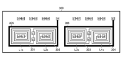
- ⁇ Transformer arrangement> 9 is a plan view (top view) showing a schematic example of a transformer arrangement in a two-channel transformer chip 300 (corresponding to the semiconductor device 5 described above).
- the transformer chip 300 in this figure has a first transformer 301, a second transformer 302, a third transformer 303, a fourth transformer 304, a first guard ring 305, a second guard ring 306, pads a1 to a8, pads b1 to b8, pads c1 to c4, and pads d1 to d4.
- pads a1 and b1 are connected to one end of the secondary coil L1s forming the first transformer 301, and pads c1 and d1 are connected to the other end of the secondary coil L1s.
- Pads a2 and b2 are connected to one end of the secondary coil L2s forming the second transformer 302, and pads c1 and d1 are connected to the other end of the secondary coil L2s.
- pads a3 and b3 are connected to one end of the secondary coil L3s forming the third transformer 303, and pads c2 and d2 are connected to the other end of the secondary coil L3s.
- Pads a4 and b4 are connected to one end of the secondary coil L4s forming the fourth transformer 304, and pads c2 and d2 are connected to the other end of the secondary coil L4s.
- the primary coil forming the first transformer 301, the primary coil forming the second transformer 302, the primary coil forming the third transformer 303, and the primary coil forming the fourth transformer 304 are not shown in this diagram.
- the primary coils basically have the same configuration as the secondary coils L1s to L4s, and are arranged directly below each of the secondary coils L1s to L4s, facing the secondary coils L1s to L4s, respectively.
- pads a5 and b5 are connected to one end of the primary coil forming the first transformer 301, and pads c3 and d3 are connected to the other end of the primary coil.
- Pads a6 and b6 are connected to one end of the primary coil forming the second transformer 302, and pads c3 and d3 are connected to the other end of the primary coil.
- pads a7 and b7 are connected to one end of the primary coil forming the third transformer 303, and pads c4 and d4 are connected to the other end of the primary coil. Furthermore, pads a8 and b8 are connected to one end of the primary coil forming the fourth transformer 304, and pads c4 and d4 are connected to the other end of the primary coil.
- pads a5 to a8, pads b5 to b8, pads c3 and c4, and pads d3 and d4 are pulled out from the inside of the transformer chip 300 to the surface through vias (not shown).
- pads a1 to a8 correspond to first current supply pads
- pads b1 to b8 correspond to first voltage measurement pads
- pads c1 to c4 correspond to second current supply pads
- pads d1 to d4 correspond to second voltage measurement pads.
- the series resistance component of each coil can be accurately measured during the defective product inspection. This makes it possible to not only reject defective products where each coil has a break in the wire, but also to appropriately reject defective products where the resistance value of each coil is abnormal (for example, a short circuit between coils), which in turn makes it possible to prevent defective products from being released onto the market.
- the above-mentioned multiple pads can be used as a connection means with the primary side chip and the secondary side chip (for example, the aforementioned controller chip 210 and driver chip 220).
- pads a1 and b1, pads a2 and b2, pads a3 and b3, and pads a4 and b4 may be connected to the signal input or output terminals of the secondary chip, respectively.
- pads c1 and d1, and pads c2 and d2 may be connected to the common voltage application terminal (GND2) of the secondary chip, respectively.
- pads a5 and b5, pads a6 and b6, pads a7 and b7, and pads a8 and b8 may be connected to the signal input or output terminals of the primary chip, respectively.
- pads c3 and d3, and pads c4 and d4 may be connected to the common voltage application terminal (GND1) of the primary chip, respectively.
- the first transformer 301 to the fourth transformer 304 are arranged in a coupled manner according to the respective signal transmission directions.
- the first transformer 301 and the second transformer 302 which transmit signals from the primary chip to the secondary chip are arranged as a first pair by the first guard ring 305.
- the third transformer 303 and the fourth transformer 304, which transmit signals from the secondary chip to the primary chip are arranged as a second pair by the second guard ring 306.
- the reason for this coupling is to ensure a sufficient withstand voltage between the primary coil and the secondary coil when the primary coil and the secondary coil that respectively form the first transformer 301 to the fourth transformer 304 are stacked vertically on the substrate of the transformer chip 300.
- the first guard ring 305 and the second guard ring 306 are not necessarily essential components.
- the first guard ring 305 and the second guard ring 306 may be connected to a low impedance wiring such as a ground terminal via pads e1 and e2, respectively.
- pads c1 and d1 are shared between the secondary coil L1s and secondary coil L2s.
- Pads c2 and d2 are shared between the secondary coil L3s and secondary coil L4s.
- Pads c3 and d3 are shared between the primary coil L1p and primary coil L2p.
- Pads c4 and d4 are shared between the corresponding primary coils. This configuration makes it possible to reduce the number of pads and miniaturize the transformer chip 300.
- transformer arrangement in this diagram is merely one example, and the number, shape, and arrangement of the coils, as well as the arrangement of the pads, are optional.
- chip structure and transformer arrangement that have been explained so far can be applied to semiconductor devices in general that integrate coils on a semiconductor chip.
- ⁇ Signal Transmission Device (First Embodiment)> 10 is a diagram showing a first embodiment of a signal transmission device 400.
- the signal transmission device 400 of this embodiment is mounted on an electronic device A together with various discrete components (a switch element TR1, resistors R0 to R3, a sense resistor Rs, and a capacitor C1).
- the signal transmission device 400 is a semiconductor integrated circuit device (a so-called insulated gate driver IC) that generates an output pulse signal OUT according to an input pulse signal IN while isolating input from output, and drives the switch element TR1.
- the signal transmission device 400 includes a drive circuit 410 as a means for driving the switch element TR1.
- the signal transmission device 400 may be configured in the same manner as the previously mentioned signal transmission device 200 (FIG. 1), by sealing in a single package a first chip (corresponding to the previously mentioned controller chip 210) that generates a transmission pulse signal from an input pulse signal IN, a second chip (corresponding to the previously mentioned driver chip 220) that generates an output pulse signal OUT from a received pulse signal, and a third chip (corresponding to the previously mentioned transformer chip 230) that transmits the transmission pulse signal as a received pulse signal while insulating the first chip from the second chip.
- the drive circuit 410 may be integrated into the second chip.
- the signal transmission device 400 also includes external terminals 421 to 427 as means for establishing electrical connection with the outside of the device.
- External terminal 421 is a secondary power supply terminal (VCC2 pin).
- External terminal 422 is an upper output terminal (OUTH pin).
- External terminal 423 is a negative power supply terminal (VEE2 pin).
- External terminal 424 is a first lower output terminal (OUTL pin).
- External terminal 425 is a second lower output terminal (PROOUT pin).
- External terminal 426 is a current detection terminal (ISENSE pin).
- External terminal 427 is a secondary ground terminal (GND2 pin).
- External terminal 421 is connected to the application terminal of power supply voltage VCC2 and the first terminal of capacitor C1.
- the second terminal of capacitor C1 is connected to a reference potential terminal (e.g., node HVDC-).
- External terminal 422 is connected to the first terminal of resistor R0.
- External terminal 423 is connected to the application terminal of negative power supply voltage VEE2.
- External terminal 424 is connected to a first end of resistor R1 (corresponding to a first external resistor).
- External terminal 425 is connected to a first end of resistor R2 (corresponding to a second external resistor).
- Resistor R2 should have a higher resistance value than resistor R1.
- External terminal 426 is connected to a first end of resistor R3.
- External terminal 427 is connected to node HVDC-.
- the switch element TR1 is a power transistor that connects/disconnects the node HVDC+ and the node HVDC-.
- the switch element TR1 may be the upper switch element and the lower switch element of a half-bridge output stage or a full-bridge output stage.
- the half-bridge output stage or the full-bridge output stage may be used as a load driving means such as a motor driver, or may be used as a power conversion means such as an inverter.
- the switch element TR1 may be an IGBT.
- the collector of the switch element TR1 is connected to the node HVDC+.
- the first emitter of the switch element TR1 is connected to the node HVDC-.
- the second emitter (so-called emitter sense) of the switch element TR1 is connected to the first end of the sense resistor Rs and the second end of the resistor R3.
- the second end of the sense resistor Rs is connected to the node HVDC-.
- a body diode with the collector as the cathode and the first emitter as the anode is associated with the switch element TR1.
- the external terminal 424 corresponds to the first external terminal connected to the application terminal of the output pulse signal OUT via the resistor R1.
- the external terminal 425 corresponds to the second external terminal connected to the application terminal of the output pulse signal OUT via the resistor R2, which has a higher resistance value than the resistor R1.
- the switch element TR1 may be replaced with a MOSFET [metal oxide semiconductor field effect transistor] or the like.
- MOSFET metal oxide semiconductor field effect transistor
- the drive circuit 410 includes logic 411, a transistor 412 (e.g., a PMOSFET), transistors 413 and 414 (e.g., an NMOSFET), a controller 415, and a short circuit detection circuit 416 (e.g., a comparator).
- a transistor 412 e.g., a PMOSFET
- transistors 413 and 414 e.g., an NMOSFET
- a controller 415 e.g., a controller 415
- a short circuit detection circuit 416 e.g., a comparator
- the logic 411 generates gate signals GH and GL1 for the transistors 412 and 413, respectively, in response to the input pulse signal IN (more precisely, the received pulse signal transmitted in an insulated manner from the controller chip).
- the transistor 412 is an upper switch element that, together with the transistor 413, forms a half-bridge output stage of the drive circuit 410.
- the drain of the transistor 412 is connected to the external terminal 422.
- the source of the transistor 412 is connected to the external terminal 421.
- the on-voltage corresponds to the high level of the output pulse signal OUT, that is, the logic level when the switch element TR1 is on.
- the gate of the transistor 412 is connected to the application terminal of the gate signal GH.
- the transistor 412 is in the on state when the gate signal GH is at a low level. On the other hand, the transistor 412 is in the off state when the gate signal GH is at a high level.
- the transistor 413 (corresponding to the first transistor) is a lower-side switch element that forms a half-bridge output stage of the drive circuit 410 together with the transistor 412.
- the drain of the transistor 413 is connected to the external terminal 424.
- the source of the transistor 413 is connected to the external terminal 423.
- the off voltage corresponds to the low level of the output pulse signal OUT, that is, the logic level when the switch element TR1 is off.
- the gate of the transistor 413 is connected to the application terminal of the gate signal GL1.
- the transistor 413 is in the on state when the gate signal GL1 is at a high level. On the other hand, the transistor 413 is in the off state when the gate signal GL1 is at a low level.
- Transistor 414 (corresponding to the second transistor) is a second lower-side switch element used for soft turn-off control when a short circuit is detected.
- the drain of transistor 414 is connected to external terminal 424.
- the gate of transistor 414 is connected to the application terminal of gate signal GL2.
- Transistor 414 is turned on when gate signal GL2 is at a high level. On the other hand, transistor 414 is turned off when gate signal GL2 is at a low level.
- transistor 414 may be an element having a smaller element size and a higher on-resistance value than transistor 413.
- the controller 415 forcibly switches switch element TR1 to the off state when a short circuit in the load is detected.
- the controller 415 may set the slew rate to a first set value SR1 until a predetermined first time T1 has elapsed since the short-circuit state of the load is detected.
- the controller 415 may also set the slew rate to a second set value SR2, which is smaller than the first set value SR1, until a predetermined second time T2 has elapsed since the first time T1 has elapsed.
- At least one of the first time T1 and the second time T2 may be a variable value.
- the slew rate of the output pulse signal OUT at the time of the fall becomes the first set value SR1 according to the resistor R1.
- the slew rate at the time when the output pulse signal OUT falls becomes the second set value SR2 according to the resistor R2.
- the resistor R2 has a higher resistance value than the resistor R1. Therefore, the second set value SR2 of the slew rate becomes a value smaller than the first set value SR1 mentioned above.
- the controller 415 may also be understood as part of the logic 411.
- the short circuit detection circuit 416 detects a short circuit state of the load by monitoring the sense voltage Vs and generates a short circuit detection signal SCP. In accordance with this diagram, the short circuit detection circuit 416 compares the sense voltage Vs applied to the external terminal 426 with a predetermined threshold voltage Vth1 to generate the short circuit detection signal SCP.
- the sense current Is is proportional to the output current Ie flowing through the first emitter of the switch element TR1. Therefore, the sense voltage Vs corresponds to a sense signal according to the output current Ie flowing through the switch element TR1. In other words, the sense voltage Vs becomes higher as the output current Ie becomes larger, and becomes lower as the output current Ie becomes smaller.
- the short circuit detection signal SCP is at a logic level (e.g. low level) when no abnormality is detected.
- the short-circuit detection signal SCP becomes the logic level (e.g., high level) when an abnormality is detected.
- the short circuit detection circuit 416 employs the so-called emitter sense method as a method for detecting a short circuit in the load.
- the emitter sense method by monitoring the sense voltage Vs, it is possible to detect whether or not an excessive short circuit current is flowing through the switch element TR1, i.e., whether or not the load is in a short circuit state.
- ⁇ Short Circuit Detection Operation (First Embodiment)> 11 is a diagram showing an example of a short circuit detection operation in the first embodiment.
- an input pulse signal IN an upper output enable signal OUTH_EN, a lower output enable signal OUTL_EN, a first short circuit protection enable signal TLTOG_EN, a second short circuit protection enable signal ISSD_EN, an output pulse signal OUT, a sense voltage Vs, a short circuit detection signal SCP, and a fault signal FAULT are depicted.
- the upper output enable signal OUTH_EN and the lower output enable signal OUTL_EN can each be understood as an internal signal of the logic 411.
- the first short circuit protection enable signal TLTOG_EN and the second short circuit protection enable signal ISSD_EN can each be understood as an internal signal of the controller 415.
- the input pulse signal IN is raised to a high level.
- the upper output enable signal OUTH_EN is raised to a high level, and the lower output enable signal OUTL_EN is lowered to a low level.
- transistor 412 is turned on, and transistors 413 and 414 are both turned off.
- the sense voltage Vs exceeds the threshold voltage Vth1 due to an increase in the output current Ie (and therefore the sense current Is) caused by the short circuit of the load.
- the first short-circuit protection enable signal TLTOG_EN is set to a high level over the first time T1, while the second short-circuit protection enable signal ISSD_EN is maintained at a low level.
- the transistor 413 is turned on, while the transistor 414 is maintained in an off state.
- the first short-circuit protection enable signal TLTOG_EN is set to low level and the second short-circuit protection enable signal ISSD_EN is set to high level for the second time T2.
- the time t15 to t16 corresponds to the time Tc during which the transistors 413 and 414 are prevented from being turned on simultaneously.
- two-stage soft turn-off control is implemented after a short circuit condition of the load is detected.
- the output pulse signal OUT is pulled down at a relatively large slew rate. Therefore, the on-resistance value of the switch element TR1 increases without delay. As a result, the excessive short-circuit current flowing through the switch element TR1 is quickly suppressed.
- the output pulse signal OUT is pulled down at a relatively small slew rate.
- the output current Ie is first quickly suppressed in the first stage (T1), and then the second stage (T2) switches to suppressing voltage surges. Therefore, it is possible to achieve both voltage surge suppression and loss reduction.
- the first time T1 and the second time T2 may be set arbitrarily using a timer.
- the first set value SR1 and the second set value SR2 of the slew rate may be adjusted arbitrarily using external resistors R1 and R2, respectively.
- the lower output enable signal OUTL_EN is raised to a high level.
- the transistor 413 is turned on. Therefore, the output pulse signal OUT drops more steeply compared to the second stage (T2).
- the occurrence of an abnormality is notified to the outside of the signal transmission device 400.
- times t15 to t18 correspond to the internal processing time Td of the logic 411.
- the timing at which the logical level of the fault signal FAULT is switched is not limited to the above.
- the logical level of the fault signal FAULT may be lowered to a low level using the rising edge of the short circuit detection signal SCP at time t14 as a trigger.
- the sense voltage Vs falls below the threshold voltage Vth1.
- ⁇ Signal Transmission Device (Second Embodiment)> 12 is a diagram showing a second embodiment of a signal transmission device 400.
- the signal transmission device 400 of this embodiment is based on the first embodiment (FIG. 10) described above, but the short circuit detection method is changed.
- the drive circuit 410 of this embodiment includes a short circuit detection circuit 417 (e.g., a comparator), a current source 418, and an external terminal 428 instead of the short circuit detection circuit 416 and external terminal 426 described above.
- a resistor R4 and a diode D1 are depicted as discrete components externally attached to the signal transmission device 400.
- the short circuit detection circuit 417 detects a short circuit state of the load by monitoring the desaturation between the collector and emitter of the switch element TR1, and generates a short circuit detection signal SCP. In accordance with this diagram, the short circuit detection circuit 417 generates the short circuit detection signal SCP by comparing the desaturation detection voltage Vdesut applied to the external terminal 428 with a predetermined threshold voltage Vth2.
- Current source 418 is connected between the application terminal of power supply voltage VCC2 and external terminal 428, and generates bias current Idesut.
- the short-circuit detection signal SCP becomes the logic level (e.g., high level) when an abnormality is detected.
- the short circuit detection circuit 417 employs the so-called DESAT method as a method for detecting a short circuit in the load.
- the DESAT method can detect whether an excessive short circuit current is flowing through the switch element TR1, i.e., whether the load is in a short circuit state, by monitoring the non-saturation between the collector and emitter of the switch element TR1.
- ⁇ Short Circuit Detection Operation (Second Embodiment)> 13 is a diagram showing an example of a short circuit detection operation in the second embodiment.
- an input pulse signal IN an upper output enable signal OUTH_EN, a lower output enable signal OUTL_EN, a first short circuit protection enable signal TLTOG_EN, a second short circuit protection enable signal ISSD_EN, an output pulse signal OUT, a desaturation detection voltage Vdesat, a bias current enable signal Idesat_EN, a short circuit detection signal SCP, and a fault signal FAULT are depicted.
- the upper output enable signal OUTH_EN and the lower output enable signal OUTL_EN can each be understood as an internal signal of the logic 411.
- the first short circuit protection enable signal TLTOG_EN, the second short circuit protection enable signal ISSD_EN, and the bias current enable signal Idesat_EN can each be understood as an internal signal of the controller 415.
- the input pulse signal IN is raised to a high level.
- the upper output enable signal OUTH_EN is raised to a high level, and the lower output enable signal OUTL_EN is lowered to a low level.
- transistor 412 is turned on, and transistors 413 and 414 are both turned off.
- the bias current enable signal Idesat_EN is set to a low level from time t21 until a predetermined waiting time Tf has elapsed. During this time, the generation of the bias current Idesat is stopped. Therefore, the desaturation detection voltage Vdesat is maintained at 0 V.
- the bias current enable signal Idesat_EN is raised to a high level, and the generation of the bias current Idesat begins. As a result, the desaturation detection voltage Vdesat rises.
- the desaturation detection voltage Vdesat exceeds the threshold voltage Vth2.
- the output pulse signal OUT is pulled down at a relatively small slew rate (SR2).
- SR2 slew rate
- ⁇ Application to vehicles> 14 is a diagram showing the external appearance of a vehicle B.
- Vehicle B of this configuration example is equipped with various electronic devices that operate by receiving power supply from a battery.
- Vehicle B includes not only engine vehicles, but also electric vehicles (BEVs [battery electric vehicles], HEVs [hybrid electric vehicles], PHEVs/PHVs (plug-in hybrid electric vehicles/plug-in hybrid vehicles), and xEVs such as FCEVs/FCVs (fuel cell electric vehicles/fuel cell vehicles)).
- BEVs battery electric vehicles
- HEVs hybrid electric vehicles
- PHEVs/PHVs plug-in hybrid electric vehicles/plug-in hybrid vehicles
- FCEVs/FCVs fuel cell electric vehicles/fuel cell vehicles
- the signal transmission device 200 or 400 described above can be incorporated into any of the electronic devices installed in vehicle B.
- the drive circuit disclosed in this specification includes a short circuit detection circuit configured to detect a short circuit state in which an excessive short circuit current may flow through a switch element, and a controller configured to forcibly turn off the switch element when the short circuit state is detected, and the controller is configured to switch an output pulse signal for driving the switch element from an on logic level to an off logic level while gradually lowering the slew rate when forcibly turning off the switch element (first configuration).
- the controller may be configured to set the slew rate to a first set value until a predetermined first time has elapsed since the short-circuit state was detected, and to set the slew rate to a second set value smaller than the first set value until a predetermined second time has elapsed since the first time has elapsed (second configuration).
- At least one of the first time and the second time may be a variable value (third configuration).
- the drive circuit according to the second or third configuration may further include a first external terminal configured to be connected to the application end of the output pulse signal via a first external resistor, a second external terminal configured to be connected to the application end of the output pulse signal via a second external resistor having a resistance value higher than that of the first external resistor, a first transistor connected between the first external terminal and an application end of an off voltage corresponding to the logic level when the output pulse signal is off, and a second transistor connected between the second external terminal and the application end of the off voltage.
- the controller may be configured to keep the first transistor in an on state and the second transistor in an off state until the first time has elapsed since the short circuit state is detected, and to keep the first transistor in an off state and the second transistor in an on state until the second time has elapsed since the first time has elapsed (fourth configuration).
- the short circuit detection circuit may be configured to monitor a sense signal corresponding to the output current flowing through the switch element (fifth configuration).
- the short circuit detection circuit may be configured to monitor a non-saturated state between both ends of the switch element (sixth configuration).
- the drive circuit according to any one of the first to sixth configurations may be further configured (seventh configuration) to include logic configured to generate a fault signal for reporting the short-circuit state.
- the signal transmission device disclosed in this specification is composed of a first chip configured to generate a transmission pulse signal from an input pulse signal, a second chip configured to generate the output pulse signal from a received pulse signal, and a third chip configured to transmit the transmission pulse signal as the received pulse signal while insulating the first chip from the second chip, all sealed in a single package, and a drive circuit according to any one of the first to seventh configurations above is configured to be integrated into the second chip (eighth configuration).
- the electronic device disclosed in this specification has a configuration (ninth configuration) that includes a signal transmission device having the eighth configuration and the switch element configured to be driven by the drive circuit.
- the vehicle disclosed in this specification is configured to include electronic equipment according to the ninth configuration (tenth configuration).
Landscapes
- Engineering & Computer Science (AREA)
- Power Engineering (AREA)
- Semiconductor Integrated Circuits (AREA)
Priority Applications (2)
| Application Number | Priority Date | Filing Date | Title |
|---|---|---|---|
| JP2024576160A JPWO2024166561A1 (https=) | 2023-02-07 | 2023-12-22 | |
| US19/290,590 US20250364799A1 (en) | 2023-02-07 | 2025-08-05 | Driving circuit, signal transmission device, electronic device, and vehicle |
Applications Claiming Priority (2)
| Application Number | Priority Date | Filing Date | Title |
|---|---|---|---|
| JP2023-016511 | 2023-02-07 | ||
| JP2023016511 | 2023-02-07 |
Related Child Applications (1)
| Application Number | Title | Priority Date | Filing Date |
|---|---|---|---|
| US19/290,590 Continuation US20250364799A1 (en) | 2023-02-07 | 2025-08-05 | Driving circuit, signal transmission device, electronic device, and vehicle |
Publications (1)
| Publication Number | Publication Date |
|---|---|
| WO2024166561A1 true WO2024166561A1 (ja) | 2024-08-15 |
Family
ID=92262930
Family Applications (1)
| Application Number | Title | Priority Date | Filing Date |
|---|---|---|---|
| PCT/JP2023/046196 Ceased WO2024166561A1 (ja) | 2023-02-07 | 2023-12-22 | 駆動回路、信号伝達装置、電子機器、車両 |
Country Status (3)
| Country | Link |
|---|---|
| US (1) | US20250364799A1 (https=) |
| JP (1) | JPWO2024166561A1 (https=) |
| WO (1) | WO2024166561A1 (https=) |
Citations (3)
| Publication number | Priority date | Publication date | Assignee | Title |
|---|---|---|---|---|
| JP2017174885A (ja) * | 2016-03-22 | 2017-09-28 | ルネサスエレクトロニクス株式会社 | 半導体装置 |
| WO2022196091A1 (ja) * | 2021-03-16 | 2022-09-22 | ローム株式会社 | 絶縁ゲートドライバ、トラクションインバータ、電動車 |
| WO2022196092A1 (ja) * | 2021-03-16 | 2022-09-22 | ローム株式会社 | 絶縁ゲートドライバ、トラクションインバータ、電動車 |
-
2023
- 2023-12-22 JP JP2024576160A patent/JPWO2024166561A1/ja active Pending
- 2023-12-22 WO PCT/JP2023/046196 patent/WO2024166561A1/ja not_active Ceased
-
2025
- 2025-08-05 US US19/290,590 patent/US20250364799A1/en active Pending
Patent Citations (3)
| Publication number | Priority date | Publication date | Assignee | Title |
|---|---|---|---|---|
| JP2017174885A (ja) * | 2016-03-22 | 2017-09-28 | ルネサスエレクトロニクス株式会社 | 半導体装置 |
| WO2022196091A1 (ja) * | 2021-03-16 | 2022-09-22 | ローム株式会社 | 絶縁ゲートドライバ、トラクションインバータ、電動車 |
| WO2022196092A1 (ja) * | 2021-03-16 | 2022-09-22 | ローム株式会社 | 絶縁ゲートドライバ、トラクションインバータ、電動車 |
Also Published As
| Publication number | Publication date |
|---|---|
| JPWO2024166561A1 (https=) | 2024-08-15 |
| US20250364799A1 (en) | 2025-11-27 |
Similar Documents
| Publication | Publication Date | Title |
|---|---|---|
| US12278482B2 (en) | Isolated gate driver, traction inverter, and electric vehicle | |
| US12407242B2 (en) | Isolated gate driver, traction inverter, and electric vehicle | |
| JP7820317B2 (ja) | トランスチップ、信号伝達装置 | |
| WO2023074137A1 (ja) | トランスチップ、信号伝達装置 | |
| WO2023032430A1 (ja) | ゲートドライバ | |
| JP7611241B2 (ja) | パルス受信回路、信号伝達装置 | |
| WO2024166561A1 (ja) | 駆動回路、信号伝達装置、電子機器、車両 | |
| JP2024116829A (ja) | 駆動回路、信号伝達装置、電子機器、車両 | |
| WO2024195368A1 (ja) | 駆動回路、信号伝達装置、電子機器、車両 | |
| US20260121553A1 (en) | Drive circuit, inverter, electronic apparatus, and vehicle | |
| JP2025163491A (ja) | 半導体装置、電子機器、車両 | |
| WO2025062993A1 (ja) | 信号伝達装置および信号伝達装置を備えた電子機器、並びに電子機器を備えた車両 | |
| US20260017162A1 (en) | Signal transmission device, electronic device, and vehicle | |
| JP2025163490A (ja) | 半導体装置、電子機器、車両 | |
| US20250015787A1 (en) | Pulse drive circuit and signal transmission device | |
| US20260045785A1 (en) | Signal transmission device, electronic device and vehicle | |
| JP2026028351A (ja) | 信号伝達装置、電子機器、および車両 | |
| WO2024181002A1 (ja) | 駆動回路、信号伝達装置、電子機器、車両 | |
| JP2025079972A (ja) | 信号伝達装置、電子機器及び車両 | |
| JP2025176835A (ja) | ドライバ、信号伝達装置、電子機器、車両 | |
| JP2024123430A (ja) | 駆動回路、信号伝達装置、電子機器、車両 | |
| JP2026017639A (ja) | 半導体装置及びスイッチング装置 | |
| WO2025105289A1 (ja) | 半導体装置、電子機器、車両 | |
| JP2024141350A (ja) | ロジック、信号伝達装置、電子機器、車両 | |
| WO2025028104A1 (ja) | 信号伝達装置、電子機器、車両 |
Legal Events
| Date | Code | Title | Description |
|---|---|---|---|
| 121 | Ep: the epo has been informed by wipo that ep was designated in this application |
Ref document number: 23921379 Country of ref document: EP Kind code of ref document: A1 |
|
| ENP | Entry into the national phase |
Ref document number: 2024576160 Country of ref document: JP Kind code of ref document: A |
|
| WWE | Wipo information: entry into national phase |
Ref document number: 2024576160 Country of ref document: JP |
|
| NENP | Non-entry into the national phase |
Ref country code: DE |
|
| 122 | Ep: pct application non-entry in european phase |
Ref document number: 23921379 Country of ref document: EP Kind code of ref document: A1 |