WO2024166350A1 - Dispositif de guidage de lumière et son procédé de fabrication - Google Patents
Dispositif de guidage de lumière et son procédé de fabrication Download PDFInfo
- Publication number
- WO2024166350A1 WO2024166350A1 PCT/JP2023/004532 JP2023004532W WO2024166350A1 WO 2024166350 A1 WO2024166350 A1 WO 2024166350A1 JP 2023004532 W JP2023004532 W JP 2023004532W WO 2024166350 A1 WO2024166350 A1 WO 2024166350A1
- Authority
- WO
- WIPO (PCT)
- Prior art keywords
- light
- section
- path
- guiding substrate
- substrate
- Prior art date
- Legal status (The legal status is an assumption and is not a legal conclusion. Google has not performed a legal analysis and makes no representation as to the accuracy of the status listed.)
- Ceased
Links
Images


Classifications
-
- G—PHYSICS
- G02—OPTICS
- G02B—OPTICAL ELEMENTS, SYSTEMS OR APPARATUS
- G02B27/00—Optical systems or apparatus not provided for by any of the groups G02B1/00 - G02B26/00, G02B30/00
- G02B27/02—Viewing or reading apparatus
-
- H—ELECTRICITY
- H04—ELECTRIC COMMUNICATION TECHNIQUE
- H04N—PICTORIAL COMMUNICATION, e.g. TELEVISION
- H04N13/00—Stereoscopic video systems; Multi-view video systems; Details thereof
- H04N13/30—Image reproducers
- H04N13/332—Displays for viewing with the aid of special glasses or head-mounted displays [HMD]
- H04N13/344—Displays for viewing with the aid of special glasses or head-mounted displays [HMD] with head-mounted left-right displays
-
- H—ELECTRICITY
- H04—ELECTRIC COMMUNICATION TECHNIQUE
- H04N—PICTORIAL COMMUNICATION, e.g. TELEVISION
- H04N5/00—Details of television systems
- H04N5/64—Constructional details of receivers, e.g. cabinets or dust covers
Definitions
- the present invention relates to a light guide device for use in an augmented reality system and a method for manufacturing the same.
- Augmented reality systems are used to display images of virtual objects as part of or overlaid on the surrounding environment, generating a virtual image of an augmented reality environment.
- Augmented reality systems may, for example, be realized as a head-mounted display or other form of wearable device.
- the augmented reality system includes a light source that generates a virtual image, a light entrance section that captures the generated virtual image, a light guide section that propagates the image captured in the light entrance section as a light beam, and a light exit section that receives the light beam from the light guide section, reconstructs an image from the light beam, and provides the image to the user.
- the light entrance section, light exit section, and light guide section are collectively referred to as a light guide device.
- Patent Documents 1-3 Various light guide devices have been developed to date (Patent Documents 1-3). However, no light guide device has been developed that has a sufficiently high efficiency of using light from a light source.
- the light-guiding device includes a light-guiding substrate that propagates light by internal reflection, a light entrance section having a first portion and a second portion that are one-dimensional diffraction gratings provided on the light-guiding substrate, the first portion being configured to propagate received light as a first light beam along a first path within the light-guiding substrate, and the second portion being configured to propagate received light as a second light beam along a second path within the light-guiding substrate, a first folding portion that is a one-dimensional diffraction grating provided on the light-guiding substrate and that is configured to change the direction of the first path of the first light beam, and a one-dimensional diffraction grating provided on the light-guiding substrate.
- the device includes a second folding section configured to change the direction of the second path of the second light beam, and a two-dimensional diffraction grating provided on the light guide substrate, the light emitting section configured to receive the first beam from the first folding section and the second beam from the second folding section, combine the first and second beams, and emit them to the outside of the light guide substrate, and on the surface of the light guide substrate, the center of the smallest circle that includes the first portion is farther from the light emitting section than the center of the smallest circle that includes the second portion, and the first path is configured to pass through the region of the light guide substrate in which the second portion is provided.
- the above light guiding device is configured such that the first path passes through the region of the light guiding substrate in which the second portion is provided, and therefore light rays propagating within the light guiding substrate as first-order diffracted light of both the first portion and the second portion can become stray light.
- Such stray light is peculiar to the above light guiding device. Therefore, there is a need for a light guiding device and a manufacturing method thereof that includes a stray light prevention structure for stray light propagating within the light guiding substrate as first-order diffracted light of both the first portion and the second portion.
- the objective of the present invention is to provide a light-guiding device equipped with a stray light prevention structure for preventing stray light propagating within a light-guiding substrate as first-order diffracted light from both the first and second parts of the light entrance section, and a method for manufacturing the same.
- the light-guiding device of the first aspect of the present invention is a light-guiding substrate that propagates light by internal reflection, and a light entrance section that includes a first portion and a second portion that are one-dimensional diffraction gratings provided on the light-guiding substrate, the first portion being configured to propagate received light as a first light beam along a first path within the light-guiding substrate, and the second portion being configured to propagate received light as a second light beam along a second path within the light-guiding substrate, and the one-dimensional diffraction grating provided on the light-guiding substrate.
- a first folding portion configured to change a direction of the first path of the first light beam, a one-dimensional diffraction grating provided on the light guiding substrate, a second folding portion configured to change a direction of the second path of the second light beam, and a two-dimensional diffraction grating provided on the light guiding substrate, a light exit portion configured to receive the first beam from the first folding portion and the second beam from the second folding portion, combine the first and second beams, and exit the light guiding substrate from the light guiding substrate.
- the light guiding device is configured such that, on a surface of the light guiding substrate, a center of a smallest circle that includes the first portion is farther from the light exit portion than a center of a smallest circle that includes the second portion, and the first path passes through a region of the light guiding substrate in which the second portion is provided.
- the light guide device has a stray light prevention structure in an area outside the first path and the second path, within the range of the path of a light ray that can be incident on the first portion, propagate as first-order diffracted light in both the first portion and the second portion, and reach the light exit portion.
- the light guide device of this embodiment is provided with a stray light prevention structure in an area outside the first path and the second path within the range of the path of a light ray that can enter the first portion, propagate as first-order diffracted light of both the first portion and the second portion, and reach the light exit portion, so that stray light that propagates within the light guide substrate as first-order diffracted light of both the first portion and the second portion can be effectively prevented.
- a method for manufacturing a light-guiding device includes a light-guiding substrate that propagates light by internal reflection, a light entrance portion having a first portion and a second portion that are one-dimensional diffraction gratings provided on the light-guiding substrate, the first portion being configured to propagate received light as a first light beam along a first path within the light-guiding substrate, and the second portion being configured to propagate received light as a second light beam along a second path within the light-guiding substrate, a first folding portion that is a one-dimensional diffraction grating provided on the light-guiding substrate and that is configured to change the direction of the first path of the first light beam, and a one-dimensional diffraction grating provided on the light-guiding substrate.
- a second folding portion configured to change the direction of the second path of the second light beam; and a two-dimensional diffraction grating provided on the light guiding substrate, the second folding portion configured to receive the first beam from the first folding portion and the second beam from the second folding portion, combine the first and second beams, and emit them to the outside of the light guiding substrate, wherein on a surface of the light guiding substrate, a center of the smallest circle that includes the first portion is farther from the light exit portion than a center of the smallest circle that includes the second portion, and the first path is configured to pass through a region of the light guiding substrate in which the second portion is provided.
- the method for manufacturing the light guide device includes the steps of: determining the angle and position of an incident light ray that can propagate through the light guide substrate as first-order diffracted light of both the first and second parts; determining the range of paths of light rays that can reach the light exit section and become stray light, among the rays of incident light that can propagate through the light guide substrate as first-order diffracted light of both the first and second parts; and installing a stray light prevention structure in an area outside the first path and the second path within the range of the path of the light rays that can become stray light.
- the manufacturing method of the light guide device of this aspect determines the range of paths of light rays that may reach the light exit section and become stray light, among the rays of incident light that may propagate within the light guide substrate as first-order diffracted light of both the first and second parts, and installs a stray light prevention structure in an area outside the first and second paths within the range of the paths of the light rays that may become stray light, thereby effectively preventing stray light from propagating within the light guide substrate as first-order diffracted light of both the first and second parts.
- the intensity of the light rays within the range of the path of the light rays that may become stray light is obtained, and the stray light prevention structure is installed in the path of the light rays whose intensity is greater than a predetermined value.
- the stray light prevention structure in the step of installing the stray light prevention structure, the position of the reflection point of the total reflection of the light ray within the range of the path of the light ray that may become the stray light is obtained, and the stray light prevention structure is installed in the vicinity of the position of the total reflection point.
- stray light can be effectively prevented by providing a diffraction grating or metasurface near the reflection point of the total reflection of a light ray that could become stray light on the surface of the light-guiding substrate.
- FIG. 1 is a perspective view of a light guide device according to the present invention
- 1 is a cross-sectional view of a light guide device according to the present invention
- 4 is a flow chart for explaining a method for designing a light guide device of the present invention.
- FIG. 2 is a diagram for explaining coordinates used in this specification.
- 1 is a diagram showing a light ray emitted from the center of the light emitting surface of the light source, incident on the light receiving surface of the light incident portion, and traveling within the light guide substrate in an xz cross section.
- 1 is a diagram showing an incidence angle ⁇ ax of a light ray incident on a light guiding substrate in an xz cross section and an incidence angle ⁇ gx of a light ray on the inner surface of the light guiding substrate.
- FIG. 1 is a diagram showing an incidence angle ⁇ ay of a light ray incident on a light guiding substrate in a yz cross section and an incidence angle ⁇ gy of a light ray on the inner surface of the light guiding substrate.
- 13 is a diagram showing the relationship between the angle of incidence on the light receiving surface of the light incident portion and the angle of incidence on the inner surface of the light guide substrate in the xz cross section.
- FIG. 1A is a diagram showing a region of a light entrance portion where light rays can propagate when the angle of incidence on the inner surface of a light-guiding substrate is equal to or greater than a critical angle and the pitch is smaller than the pupil size.
- FIG. FIG. 2 is a plan view of the light guide device according to the first embodiment.
- FIG. 2 is a diagram showing an xz cross section of the light guide device of the first embodiment.
- FIG. 13 is a plan view of a light guide device of a comparative example. 1 is a diagram showing an xz cross section of a light guide device of a comparative example.
- FIG. 11 is a plan view of a light guide device according to a second embodiment.
- FIG. 11 is a plan view of a light incident portion according to a second embodiment.
- FIG. 11 is a plan view of a light guide device according to a third embodiment.
- FIG. 11 is a plan view of a light incident portion according to a third embodiment.
- FIG. 13 is a plan view of a light guide device according to a fourth embodiment.
- FIG. 13 is a plan view of a light incident portion according to a fourth embodiment.
- FIG. 13 is a plan view of a light guide device according to a fifth embodiment.
- FIG. 13 is a plan view of a light incident portion according to a fifth embodiment.
- FIG. 1 is a diagram showing an example of a light guide device having a stray light prevention structure. 1 is a flow chart for explaining a method for manufacturing the stray light prevention structure. 24 is a flowchart for explaining step S2010 of FIG. 23. 4 is a diagram showing an incident light ray incident on a position of a point P on the surface of the light guide substrate.
- FIG. 2 is a diagram showing a cross section including a point P on the surface of the light-guiding substrate and parallel to the x-axis and z-axis.
- FIG. 2 is a diagram showing a cross section including a point P on the surface of the light guide substrate and parallel to the y-axis and z-axis.
- FIG. 23 is an enlarged view of the light incident portion and its surroundings in FIG. 22 .
- 24 is a flowchart for explaining step S2020 of FIG. 23.
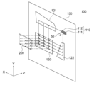
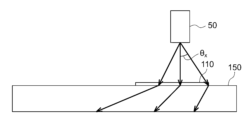
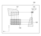
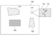
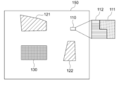
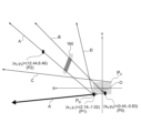
- FIG. 1 is a perspective view of a light guide device 100 according to the present invention.
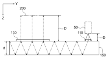
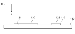
- FIG. 2 is a cross-sectional view of a light guide device 100 according to the present invention.
- the light guiding device 100 includes a light guiding substrate 150, and a light entrance section 110, a first light return section 121, a second light return section 122, and a light exit section 130 provided on the light guiding substrate 150.
- the light entrance section 110 includes a first section 111 and a second section 112, each of which is a one-dimensional surface structure type diffraction grating.
- the first light return section 121 and the second light return section 122 are each a one-dimensional surface structure type diffraction grating.
- the light exit section 130 is a two-dimensional surface structure type diffraction grating.
- the light source 50 is configured to form an image on the light entrance section 110.
- the light source 50 may be a laser light source that forms an image on the light entrance section 110 by scanning a laser beam.
- the distance between the light source 50 and the light guide substrate 150 is represented by D.
- the light received by the first portion 111 of the light entrance section 110 is taken into the light guide substrate 150 as diffracted light, and is transmitted to the first light folding section 121 by total reflection within the light guide substrate 150.
- the thickness of the light guide substrate 150 is represented by d.
- the light that reaches the first light folding section 121 has its direction of travel changed by the first light folding section 121 and is transmitted to the light exit section 130.
- the light received by the second portion 112 of the light entrance section 110 is taken into the light guide substrate 150 as diffracted light, and is transmitted to the second light folding section 122 by total reflection within the light guide substrate 150.
- the light that reaches the second light folding unit 122 has its direction of travel changed by the second light folding unit 122 and is transmitted to the light emitting unit 130.
- the light emitting unit 130 combines the light received from the first light folding unit 121 and the second light folding unit 122 to form an image in the eye box 200.
- the eye box 200 refers to an area in which no part of the image is missing even if the observer's pupil moves.
- the distance between the eye box 200 and the light guiding substrate 150 is represented by D'.
- the path of the light ray in the light guiding substrate 150 in FIG. 2 is for explaining total reflection in the light guiding substrate 150 and does not show the actual path.
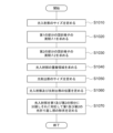
- FIG. 3 is a flow chart for explaining a method for designing the light guide device 100 of the present invention.
- the size of the light entrance portion 110 is determined in step S1010 of FIG. 3.
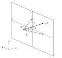
- FIG. 4 is a diagram for explaining the coordinates used in this specification.
- the x-axis is set in a direction corresponding to the horizontal direction when the light guide device 100 is in use, and the y-axis is set in a direction corresponding to the vertical direction.
- the x-axis coordinate is set so that the coordinate of the light emission section 130 is greater than the coordinate of the light incidence section 110, and the y-axis coordinate is set so that the coordinate of the light emission section 130 is smaller than the coordinate of the light incidence section 110.
- the z-axis is set to be perpendicular to both axes, with the intersection of the x-axis and y-axis as the origin.
- the x-axis and y-axis are defined on the light receiving surface of the light incident section 110, and the center of the light receiving surface is defined as the origin.
- the center of the light source 50 is located on the z-axis at a distance D from the origin.
- the z-axis coordinate is defined so that the coordinate of the center of the light source 50 is smaller than the coordinate of the origin.
- the angle of incidence of the light ray emitted from the center of the light source 50 and reaching point P on the light receiving surface of the light incident section 110 is represented by ⁇ .
- the x-axis component and y-axis component of ⁇ are represented by ⁇ x and ⁇ y, respectively.
- ⁇ x and ⁇ y are positive when the light ray travels so that the coordinate increases before entering. In FIG. 4, ⁇ x is negative and ⁇ y is positive.
- the length L1x in the x-axis direction and the length L1y in the y-axis direction of the light incidence section 110 are determined based on the following formulas.
- step S1020 of FIG. 3 the grating period ⁇ 1 of the first portion 111 of the light incidence portion 110 is determined.
- the grooves of the diffraction grating of the first portion 111 are assumed to be in the y-axis direction.
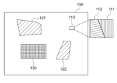
- Figure 5 is a diagram showing a ray of light emitted from the center of the light-emitting surface of the light source 50, incident on the light-receiving surface of the light entrance section 110, and traveling through the light-guiding substrate 150 in an xz cross section.
- the coordinate on the x-axis is set so that the coordinate of the light exit section 130 is greater than the coordinate of the light entrance section 110, so the direction of travel of the ray of light traveling through the light-guiding substrate 150 is the direction in which the coordinate increases along the x-axis.
- ⁇ x is negative.
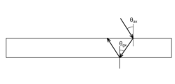
- FIG. 6 is a diagram showing the angle of incidence ⁇ ax of a light ray incident on the light guiding substrate 150 in the xz cross section, and the angle of incidence ⁇ gx on the inner surface of the light guiding substrate 150.
- the light incidence section 110 is not shown in FIG. 6.
- the grooves of the diffraction grating are perpendicular to the paper surface.
- the diffraction equation is as follows. In the case of FIG. 6, the light ray travels in the direction of decreasing x coordinate before it is incident on the light incidence section 110, so the value of ⁇ ax is negative.
- the incident angle ⁇ gx on the inner surface of the light-guiding substrate 150 when the incident angle ⁇ gx on the inner surface of the light-guiding substrate 150 is equal to or greater than the critical angle, the light beam that enters the light-guiding substrate 150 from the light-receiving surface of the light entrance section 110 can travel through the light-guiding substrate 150 while being totally reflected as shown in FIG. 2. Therefore, the incident angle ⁇ ax on the light-receiving surface of the light entrance section 110 must be determined so that the incident angle ⁇ gx on the inner surface of the light-guiding substrate 150 is equal to or greater than the critical angle.
- Equation (2) the maximum angle of incidence - ⁇ xmax in the xz cross section is substituted for ⁇ ax to find ⁇ , and this value is designated as ⁇ 1.
- ⁇ xmax is an absolute value.
- equation (1) when the grating period is ⁇ 1, ⁇ gx increases as ⁇ ax increases (the absolute value of ⁇ ax decreases). Therefore, if ⁇ ax is equal to or greater than - ⁇ xmax, ⁇ gx becomes equal to or greater than the critical angle, and the light ray can travel through the light-guiding substrate 150 while being totally reflected.
- the absolute value of the incident angle at which ⁇ gx is equal to or greater than the critical angle increases by reducing the grating period.
- step S1030 of FIG. 3 the grating period ⁇ 2 of the second portion 112 of the light entrance portion 110 is found.
- the grooves of the diffraction grating of the second portion 112 are in the x-axis direction.
- the y-axis coordinate is set so that the coordinate of the light exit portion 130 is smaller than the coordinate of the light entrance portion 110, so the direction of travel of the light rays traveling within the light guide substrate 150 is the direction in which the coordinate decreases along the y-axis.
- Figure 7 is a diagram showing the angle of incidence ⁇ ay of a light ray incident on the light guiding substrate 150 in the yz cross section and the angle of incidence ⁇ gy on the inner surface of the light guiding substrate 150.
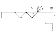
- the pitch p in Figure 7 indicates the distance between the points at which the light ray is totally reflected on the inner surface of the light guiding substrate 150 in the yz cross section shown in Figure 7.
- the light entrance section 110 is not shown in Figure 7.
- the grooves of the diffraction grating are in a direction perpendicular to the paper surface.
- the diffraction equation is as follows. In the case of Figure 7, the light ray travels in the direction of decreasing y coordinate before entering the light entrance section 110, so the value of ⁇ ay is negative.
- ⁇ ay is the incident angle in the yz cross section of the light receiving surface of the light incident portion
- ⁇ gy is the incident angle in the yz cross section of the inner surface of the light guide substrate.
- the pitch p In order to provide a stable image to the observer, the pitch p must be equal to or smaller than the pupil size.
- the angle of incidence ⁇ gy on the inner surface of the light guide substrate corresponding to the pitch p of the pupil size is called the pitch angle ⁇ p.
- the pitch angle ⁇ p is calculated from the pitch p of the pupil size by the following formula. By substituting ⁇ p for ⁇ gy in equation (1)′, the following equation is obtained.
- the grating period ⁇ is appropriately determined, and the incident angle ⁇ ay in the yz cross section of the light receiving surface of the light incident portion is calculated. If the absolute value of ⁇ ay is equal to or greater than the maximum incident angle in the yz cross section, that value is taken as ⁇ 2. If the absolute value of ⁇ ay is smaller than the maximum incident angle in the yz cross section, the grating period ⁇ is reduced to calculate ⁇ 2.
- the pitch length becomes smaller and the image becomes easier to observe. Therefore, it is preferable to increase the grating period as long as the maximum incident angle condition is satisfied.
- the relationship between the grating period and the pitch length will be explained in detail in Example 1.
- FIG. 8 is a diagram showing the relationship between the angle of incidence of the light receiving surface of the light entrance portion and the angle of incidence of the inner surface of the light guide substrate in the xz section.
- FIG. 8 shows the above relationship in Example 1, which will be described later.
- the horizontal axis of FIG. 8 indicates the angle of incidence of the light entrance portion 110 in the xz section
- the vertical axis of FIG. 8 indicates the angle of total reflection in the xz section of the inner surface of the light guide substrate. If the angle of incidence of the light receiving surface of the light entrance portion in the xz section is ⁇ acx or more, the angle of incidence of the light receiving surface of the inner surface of the light guide substrate in the xz section is equal to or greater than the critical angle.
- the pitch is smaller than the pupil size.
- ⁇ apx is the angle of incidence corresponding to the pitch angle in the xz section. In this way, the angle of incidence of the light receiving surface of the light entrance portion in the xz section must be in an angle range in which the angle of incidence of the light receiving surface of the light entrance portion in the xz section of the inner surface of the light guide substrate in the xz section is equal to or greater than the critical angle and the pitch is smaller than the pupil size.
- step S1040 of FIG. 3 the area of the light entrance section 110 that can propagate light rays so that the angle of incidence on the inner surface of the light-guiding substrate is equal to or greater than the critical angle and the pitch is smaller than the pupil size is determined.
- the condition for the incident angle on the inner surface of the light guide substrate to be equal to or larger than the critical angle can be expressed by the following formula.
- ⁇ ax is the angle of incidence of the light receiving surface of the light incident portion in the xz cross section
- ⁇ ay is the angle of incidence of the light receiving surface of the light incident portion in the yz cross section
- ⁇ is the inclination angle (counterclockwise) of the grooves of the grating from the y axis when the groove direction is approximately in the y axis direction.
- the condition for the incident angle on the inner surface of the light guide substrate to be equal to or larger than the critical angle can be expressed by the following formula.
- ⁇ ax is the angle of incidence of the light receiving surface of the light incident portion in the xz cross section
- ⁇ ay is the angle of incidence of the light receiving surface of the light incident portion in the yz cross section
- ⁇ is the inclination angle (counterclockwise) of the grooves of the grating from the x-axis when the groove direction is approximately in the x-axis direction.
- the condition of the incident angle for making the pitch in the light guide substrate equal to or smaller than the pupil size can be expressed by the following formula.
- ⁇ ax is the angle of incidence of the light receiving surface of the light incident portion in the xz cross section
- ⁇ ay is the angle of incidence of the light receiving surface of the light incident portion in the yz cross section
- ⁇ is the inclination angle (counterclockwise) of the grooves of the grating from the y axis when the groove direction is approximately in the y axis direction.
- the condition of the incident angle for making the pitch in the light guide substrate equal to or smaller than the pupil size can be expressed by the following equation.
- ⁇ ax is the angle of incidence of the light receiving surface of the light incident portion in the xz cross section
- ⁇ ay is the angle of incidence of the light receiving surface of the light incident portion in the yz cross section
- ⁇ is the inclination angle (counterclockwise) of the grooves of the grating from the x-axis when the groove direction is approximately in the x-axis direction.
- the following additional condition must be satisfied in order for the light rays to propagate so that the angle of incidence on the inner surface of the light-guiding substrate is equal to or greater than the critical angle and the pitch is smaller than the pupil size.
- the additional condition for the light beam incident on the first portion 111 can be expressed by the following equation.
- the incident angle ⁇ acx' on the light receiving surface corresponding to the critical angle is obtained by substituting ⁇ 2 for ⁇ in equation (2).
- the condition for the angle of incidence of the light beam incident on the first portion 112 can be expressed by the following equation.
- the incident angle ⁇ apy' on the light receiving surface corresponding to the critical angle is found by substituting ⁇ 1 for ⁇ in equation (3).
- FIG. 9 is a diagram showing the region of the light entrance section 110 where light rays can be propagated such that the angle of incidence on the inner surface of the light-guiding substrate is equal to or greater than the critical angle and the pitch is smaller than the pupil size.
- the x-axis of FIG. 9 represents tan( ⁇ ax), and the y-axis of FIG. 9 represents tan( ⁇ ay).
- Straight lines L1, L2, L3, and L4 in FIG. 9 represent equations (4), (5), (6), and (7), respectively.
- L1' and L4' represent equations (4)' and (7)', respectively.
- the region surrounded by straight lines L1', L2, L3, and L4' is the region where light rays can be propagated such that the angle of incidence on the inner surface of the light-guiding substrate is equal to or greater than the critical angle and the pitch is smaller than the pupil size. This region is called the overlap region.
- step S1050 of FIG. 3 the size of the light emission section 130 is determined.
- the origin of the coordinate system shown in FIG. 4 is aligned with the center of the surface of the light emitting unit 130, and the plane including the x-axis and y-axis is aligned with the surface of the light emitting unit 130.
- the center of the eye box 200 is set on the z-axis, and the eye box 200 is parallel to the plane including the x-axis and y-axis.
- the angle of incidence of the light ray emitted from point P' on the surface of the light emitting unit 130 and incident on the center of the eye box 200 is represented by ⁇ .
- the x-axis and y-axis components of ⁇ are represented by ⁇ x and ⁇ y, respectively.
- the length L2x of the light emitting portion 130 in the x-axis direction and the length L2y of the light emitting portion 130 in the y-axis direction are determined based on the following equations.
- D' is the distance from the center of the eyebox surface to the origin (the center of the light exit surface).
- L20x Eyebox length in the x-axis direction L20y Length of the eye box in the y-axis direction ⁇ xmax Maximum absolute value of ⁇ x ⁇ ymax Maximum absolute value of ⁇ y
- the light exit section 130 is a two-dimensional surface structure type diffraction grating provided on a light-guiding substrate, and the grating period of each of the two types of diffraction gratings is the same as the grating period of the one-dimensional diffraction grating of the corresponding first part 111 or second part 112 of the light entrance section 110.
- step S1060 of FIG. 3 the relative positions of the light entrance unit 110 and the light exit unit 130 are determined based on the interpupillary distance and the relative positions of the eyes and ears.
- step S1070 of FIG. 3 the division of the light entrance section 110 into the first section 111 and the second section 112 is changed while taking into account the overlapping area, and the brightness of the image observed by the pupil is evaluated by optical simulation (for example, using Virtuallab) to optimize the division.
- the shapes of the first light return section 121 and the second light return section 122 are optimized to match the light entrance section 110 divided in this way.
- the path of the light ray traveling from one of the first and second parts to the light exit section is configured not to pass through the area of the light-guiding substrate where the other part is provided.
- the light-guiding device of the present invention is configured such that, on the surface of the light-guiding substrate, the center of the smallest circle that includes the first part is farther from the light exit section than the center of the smallest circle that includes the second part, and the path of the light ray traveling from the first part to the light exit section passes through the area of the light-guiding substrate where the second part is provided. Therefore, the light-guiding device of the present invention has a much greater degree of freedom in how the light entrance section 110 is divided into the first part 111 and the second part 112 compared to the light-guiding device of the prior art.
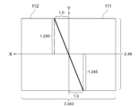
- the material of the light guide substrate 150 which includes the light entrance section 110, the first light return section 121, the second light return section 122, and the light exit section 130, is polycarbonate, and the refractive index of light with a wavelength of 520 nanometers is 1.6748.
- the thickness of the light guide substrate 150 is 1.25 millimeters. Corresponding elements in each embodiment are denoted by the same reference numerals.
- the light entrance portion 110 is rectangular, with a length in the x-axis direction of 3.343 millimeters and a length in the y-axis direction of 2.49 millimeters.
- the grooves in the first portion 111 of the light entrance portion 110 are oriented approximately along the y-axis, and the grating period is 410 nanometers.
- the grooves in the second portion 112 of the light entrance portion 110 are oriented approximately along the x-axis, and the grating period is 460 nanometers.
- the light emitting portion 130 is rectangular, with a length in the x-axis direction of 21.207 millimeters and a length in the y-axis direction of 11.929 millimeters.
- the grating period of the light emitting portion 130 in the x-axis direction is 460 nanometers, and the grating period in the y-axis direction is 460 nanometers.
- the direction of the lattice grooves is expressed as a clockwise angle based on the y-axis.
- the direction of the lattice grooves is also called the lattice direction.
- the distance D between the light source 50 and the light entrance section 110 is 6.3 millimeters, and the distance D' between the light exit section 130 and the eye box 200 is 18 millimeters.
- the diagonal angle of view of the light entrance section 110 is 30 degrees.
- the light source 50 is a laser light source, with a spot that is 0.4 millimeters in the x-axis direction and 0.8 millimeters in the y-axis direction.
- the eye box 200 is 12.8 millimeters in the x-axis direction and 7.2 millimeters in the y-axis direction.
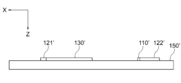
- FIG. 10 is a plan view of the light guide device 100 according to the first embodiment.
- FIG. 11 is a diagram showing the xz cross section of the light guide device 100 of the first embodiment.
- the lattice direction of the first portion 111 of the light entrance portion 110 is 0 degrees, and the lattice period is 410 nanometers.
- the lattice direction of the second portion 112 of the light entrance portion 110 is 90 degrees, and the lattice period is 460 nanometers.
- the first portion 111 and the second portion 112 are divided by a boundary line that passes through the center of the light entrance portion 110 and is parallel to the y-axis so that the areas of both portions are equal.
- the first section 111 is farther from the light exit section 130 than the second section 112, and the path of the light beam traveling from the first section 111 to the light exit section 130 passes through the region of the light guide substrate 150 in which the second section 112 is provided.
- the light beam traveling from the first section 111 to the first light folding section 121 travels in the x-axis direction so that the x-coordinate increases, and passes through the region of the light guide substrate 150 in which the second section 112 is provided.
- the light beam traveling from the second section 112 to the second light folding section 122 travels in the y-axis direction so that the y-coordinate decreases.
- the grating direction of the first optical folding section 121 is 45 degrees and the grating period is 290 nanometers.
- the grating direction of the second optical folding section 122 is 45 degrees and the grating period is 325 nanometers.
- Table 1 shows the luminance at the light receiving surface of the eye box.
- the luminance values are shown as a ratio (percentage) to the luminance of the light source. Note that the luminance values in Table 1 and the following tables were obtained by optical simulation (for example, using Virtuallab).
- the light receiving surface of the eye box 200 and the exit surface of the light emitting unit 130 are parallel, and the line connecting the centers of both surfaces is in the z-axis direction. Therefore, the position on the light receiving surface of the eye box 200 can be determined by the angle of incidence of the light ray emitted from the center of the exit surface of the light emitting unit 130.
- the horizontal angles in Table 1 represent the x-axis component of the incident angle, i.e., the coordinate in the x-axis direction
- the vertical angles in Table 1 represent the y-axis component of the incident angle, i.e., the coordinate in the y-axis direction.
- Table 2 shows pitch lengths in the light guiding substrate 150 for light rays with various angles of incidence in the light guiding device 100 of Example 1.
- the unit of the pitch length is millimeters.
- Table 3 shows pitch lengths in the light-guiding substrate 150 for light rays with various incident angles when the grating period of the second portion 111 of the light-guiding device 100 of Example 1 is changed from 460 nanometers to 410 nanometers.
- the unit of the pitch length is millimeters.
- the pitch length is increased compared to the case of Table 2 where the grating period is 460 nanometers. In this way, shortening the grating period increases the pitch length.
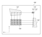
- FIG. 12 is a plan view of a light guide device 100' of a comparative example.
- FIG. 13 shows an xz cross section of a light guide device 100' as a comparative example.
- the lattice direction of the first portion 111' of the light incident portion 110' is 0 degrees, and the lattice period is 410 nanometers.
- the lattice direction of the second portion 112' of the light incident portion 110' is 90 degrees, and the lattice period is 460 nanometers.
- the first portion 111' and the second portion 112' are divided by a boundary line that passes through the center of the light incident portion 110' and is parallel to the y-axis so that the areas of both portions are equal.
- the path of the light ray traveling from one of the first and second parts to the light emitting section 130' is configured not to pass through the area of the light guiding substrate 150' that includes the other.
- the light ray traveling from the first part 111' to the first light folding section 121' travels in the x-axis direction so that the x coordinate increases
- the light ray traveling from the second part 112' to the second light folding section 122' travels in the y-axis direction so that the y coordinate decreases.
- the light ray emitted from one of the first part 111' and the second part 112' does not pass through the area of the light guiding substrate 150' that includes the other.
- the grating direction of the first optical folding section 121' is 45 degrees and the grating period is 325 nanometers.
- the grating direction of the second optical folding section 122' is 45 degrees and the grating period is 290 nanometers.
- Table 4 shows the luminance at the light receiving surface of the eye box.
- FIG. 14 is a plan view of a light guide device 100 according to the second embodiment.
- the grating direction of the first part 111 of the light entrance part 110 is 2 degrees and the grating period is 410 nanometers.
- the grating direction of the second part 112 of the light entrance part 110 is 85 degrees and the grating period is 460 nanometers.
- the first section 111 is farther from the light output section 130 than the second section 112, and the path of the light beam traveling from the first section 111 to the light output section 130 passes through the region of the light guide substrate 150 in which the second section 112 is provided.
- FIG. 15 is a plan view of the light entrance portion 110 of the second embodiment.
- the boundary between the first portion 111 and the second portion 112 consists of four line segments in the x-axis direction and five line segments in the y-axis direction.
- a straight line that passes through the origin of coordinates, which is the center of the light incident portion 110, and is parallel to the direction of the diffraction grating grooves of the first portion 111 intersects with the boundary line at four points.
- the boundary line between the first part 111 and the second part 112 does not have a single direction, and the maximum angle difference between the line segment or tangent of the boundary line and the reference direction is 90 degrees.
- the area of the light entrance section 110 away from the light exit section 130 that is occupied by the second section 112 is 4.76%.
- the area that the first section 111 occupies in the region of the light entrance section 110 that is closer to the light exit section 130 is 13.72%.
- the grating direction of the first optical folding section 121 is 46 degrees and the grating period is 285 nanometers.
- the grating direction of the second optical folding section 122 is 42.5 degrees and the grating period is 310 nanometers.
- Table 5 shows the luminance at the light receiving surface of the eye box.
- FIG. 16 is a plan view of a light guide device 100 according to the third embodiment.
- the grating direction of the first part 111 of the light entrance part 110 is 5 degrees and the grating period is 410 nanometers.
- the grating direction of the second part 112 of the light entrance part 110 is 90 degrees and the grating period is 460 nanometers.
- the light input section 110 of Example 3 is configured such that the first section 111 is farther from the light output section 130 than the second section 112, and the path of the light beam traveling from the first section 111 to the light output section 130 passes through the region of the light-guiding substrate 150 in which the second section 112 is provided.
- FIG. 17 is a plan view of the light entrance portion 110 of the third embodiment.
- the boundary between the first portion 111 and the second portion 112 consists of one line segment in the x-axis direction and two line segments in the y-axis direction.
- the boundary line between the first part 111 and the second part 112 does not have a single direction, and the maximum angle difference between the line segment or tangent of the boundary line and the reference direction is 90 degrees.
- the area of the light entrance section 110 away from the light exit section 130 that is occupied by the second section 112 is 18.21%.
- the area that the first section 111 occupies in the region of the light entrance section 110 that is closer to the light exit section 130 is 18.21%.
- the grating direction of the first optical folding section 121 is 47.5 degrees and the grating period is 286 nanometers.
- the grating direction of the second optical folding section 122 is 45 degrees and the grating period is 325 nanometers.
- Table 6 shows the luminance at the light receiving surface of the eye box.
- FIG. 18 is a plan view of a light guide device 100 according to the fourth embodiment.
- the grating direction of the first part 111 of the light entrance part 110 is 0 degrees and the grating period is 410 nanometers.
- the grating direction of the second part 112 of the light entrance part 110 is 100 degrees and the grating period is 460 nanometers.
- the light input section 110 of Example 4 is configured such that the first section 111 is farther from the light output section 130 than the second section 112, and the path of the light beam traveling from the first section 111 to the light output section 130 passes through the region of the light-guiding substrate 150 in which the second section 112 is provided.
- FIG. 19 is a plan view of the light incidence portion 110 of the fourth embodiment.
- the boundary between the first portion 111 and the second portion 112 is a line segment inclined with respect to the y-axis.
- the area of the light entrance section 110 away from the light exit section 130 that is occupied by the second section 112 is 14.96%.
- the area that the first section 111 occupies in the region of the light entrance section 110 that is closer to the light exit section 130 is 14.96%.
- the grating direction of the first light-reflecting section 121 is 45 degrees and the grating period is 290 nanometers.
- the grating direction of the second light-reflecting section 122 is 50 degrees and the grating period is 360 nanometers.
- Table 7 shows the luminance at the light receiving surface of the eye box.
- FIG. 20 is a plan view of a light guide device 100 according to a fifth embodiment.
- the grating direction of the first part 111 of the light entrance part 110 is 2 degrees and the grating period is 410 nanometers.
- the grating direction of the second part 112 of the light entrance part 110 is 85 degrees and the grating period is 460 nanometers.
- the light input section 110 of Example 5 is configured such that the first section 111 is farther from the light output section 130 than the second section 112, and the path of the light beam traveling from the first section 111 to the light output section 130 passes through the region of the light-guiding substrate 150 in which the second section 112 is provided.
- FIG. 21 is a plan view of the light entrance portion 110 of the fifth embodiment.
- the boundary between the first portion 111 and the second portion 112 consists of one line segment in the x-axis direction and three line segments in the y-axis direction.
- the boundary line between the first part 111 and the second part 112 does not have a single direction, and the maximum angle difference between the line segment or tangent of the boundary line and the reference direction is 90 degrees.
- the area of the light entrance section 110 away from the light exit section 130 that is occupied by the second section 112 is 4.28%.
- the area that the first section 111 occupies in the region of the light entrance section 110 that is closer to the light exit section 130 is 23.93%.
- the second part 112 has two parts separated from each other by the first part 111.
- the grating direction of the first optical folding section 121 is 46 degrees and the grating period is 285 nanometers.
- the grating direction of the second optical folding section 122 is 42.5 degrees and the grating period is 310 nanometers.
- Table 8 shows the luminance at the light receiving surface of the eye box.
- Table 1 of the Example 1 is compared with Table 4 of the Comparative Example. If the threshold of observable luminance is set to 0.001%, all values in Table 1 are equal to or greater than the threshold. On the other hand, in Table 2, the nine values shown in black are less than the threshold. Therefore, the light utilization efficiency of the device of the Example 1 is higher than that of the device of the Comparative Example. This is because the path of the light beam in the Example 1 has a higher diffraction efficiency at the light entrance portion 110 than the path of the light beam in the Comparative Example.
- Example 1 (Table 1) 0.007%
- Example 2 (Table 5) 0.022%
- Example 3 (Table 6) 0.015%
- Example 4 (Table 7) 0.027%
- Example 5 (Table 8) 0.022%
- Example 2-5 by appropriately defining the boundary line between the first portion 111 and the second portion 112 of the light entrance portion 110, the minimum luminance value is significantly improved compared to Example 1, in which the first portion 111 and the second portion 112 are divided by a boundary line that passes through the center of the light entrance portion 110 and is parallel to the y-axis so that the areas of both portions are equal. This is because in Example 2-5, the positioning of the first portion 111 and the second portion 112 can be flexibly changed to improve the luminance of the light receiving surface of the eye box and reduce the difference in luminance due to position on the light receiving surface of the eye box.
- FIG. 22 shows an example of a light guide device 100 that has a stray light prevention structure.
- the material of the light guide substrate 150 which includes the light entrance section 110, the first light return section 121, the second light return section 122, and the light exit section 130, is polycarbonate, and the refractive index nd of light with a wavelength of 520 nanometers is 1.6748.
- the thickness d of the light guide substrate 150 is 1.25 millimeters.
- the light source 50 (not shown) is a laser light source, and the size of the spot in the x-axis direction is 0.4 millimeters, and the size in the y-axis direction is 0.8 millimeters.
- the wavelength ⁇ of the light from the light source is 520 nanometers.
- the distance D between the light source 50 and the light entrance part 110 is 6.3 millimeters.
- the direction of the grating grooves is expressed as a clockwise angle based on the y-axis.
- the first portion 111 and the second portion 112 are divided by a boundary line that passes through the center of the light incidence portion 110 and is parallel to the y-axis so that the areas of both portions are equal.
- the light guiding device of the present invention is configured such that a first path in the light guiding substrate 150 of a light ray incident on the first portion 111 of the light entrance portion 110 passes through a region of the light guiding substrate 150 in which the second portion 112 of the light entrance portion 110 is provided. Therefore, the light ray propagating in the light guiding substrate 150 as first-order diffracted light of both the first portion 111 and the second portion 112 can become stray light.
- the stray light generated in this manner is stray light specific to the light guiding device of the present invention, and it is preferable to prevent the stray light generated in this manner.
- the area between lines C and C' is the range through which the first-order diffracted light of the first part 111 of the light entrance section 110 passes, i.e., the first path.
- the area between lines D and D' is the range through which the first-order diffracted light of the second part 112 of the light entrance section 110 passes, i.e., the second path.
- the area between lines A and B is the range of the path of light rays that can become stray light, as described below.
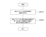
- Figure 23 is a flow chart explaining the manufacturing method of the stray light prevention structure.
- step S2010 of FIG. 23 the range of paths of light rays that may become stray light is determined.
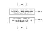
- FIG. 24 is a flow diagram for explaining step S2010 in FIG. 23.
- step S3010 of FIG. 24 the angle and position of the incident light propagating within the light-guiding substrate as first-order diffracted light from the first and second parts of the light entrance section are determined.
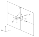
- Figure 25 is a diagram showing an incident ray of light incident at point P on the surface of light-guiding substrate 150.
- point S indicates the position of the center of the light source
- O indicates the origin on the surface of light-guiding substrate 150.
- Origin O is located at the center of light entrance section 110, and is defined as the foot of a perpendicular line drawn from point S to the surface of light-guiding substrate 150.
- the angles formed by the two straight lines projecting incident ray SP onto the xz plane and yz plane and the straight line connecting point S and point O are respectively ⁇ and ⁇ .
- the angles ⁇ and ⁇ are called the x-direction and y-direction components of the incidence angle ⁇ of incident ray SP.
- the wave number vector k in of the incident light ray can be expressed by the following equation.
- n represents the refractive index of air
- ⁇ represents the wavelength of the light from the light source.
- the diffraction condition K1 for the first order diffraction of the first portion 111 can be expressed by the following equation.
- Fig. 26 is a diagram showing a cross section including point P on the surface of light-guiding substrate 150 and parallel to the x-axis and z-axis.
- the light incident portion is not shown in Fig. 26.
- the x-direction component of the incident angle of the light ray traveling in light-guiding substrate 150 after diffraction by first portion 111 is represented as ⁇ 0 .
- Fig. 27 is a diagram showing a cross section including point P on the surface of light-guiding substrate 150 and parallel to the y-axis and z-axis. For simplicity, the light incident portion is not shown in Fig. 27.
- the y-direction component of the incident angle of the light ray traveling in light-guiding substrate 150 after diffraction by first portion 111 is represented as ⁇ 0 .
- the wave number vector k out of the above light ray can be expressed by the following equation.
- the diffraction condition K2 for the first-order diffraction of the second portion 112 can be expressed by the following equation.
- step S3020 of FIG. 23 the range of the path of the incident light ray determined in S3010 is determined by taking into consideration the positions of the first portion 111, the second portion 112, the first light returning portion 121, the second light returning portion 122, and the light emitting portion 130, and the range of the path of the light ray that may reach the light emitting portion 130 and become stray light.
- Fig. 28 is an enlarged view of the light entrance portion 110 and its surroundings in Fig. 22.
- Points P C and P D are the vertices of a rectangle that forms the boundary of the light entrance portion 110.
- the path of the light beam passing through the vicinity of the point P D of the second portion 112 is obtained by taking into consideration the formula (10).
- the above light beam is incident at the point P0 of the first portion 111 and propagates through total reflection within the light-guiding substrate 150 to the point P1 of the second portion 112 as the first-order diffracted light of the first portion 111.
- the point P1 is a point in the vicinity of the point P D.
- the above light beam propagates to the point P2 as the first-order diffracted light of the second portion 112.
- the points P1 and P2 are points where the light beam is totally reflected at the boundary surface of the substrate.
- the coordinates of points P0, P1, and P2 are expressed as (x0, y0), (x1, y1), and (x2, y2), respectively, the following equation is established.
- m0 and m1 respectively represent the number of times of total reflection of the first-order diffracted light in the first portion 111 and the second portion 112. In the case shown in FIG.
- 2dtan( ⁇ 0), 2dtan( ⁇ 0), 2dtan( ⁇ 1) and 2dtan( ⁇ 1) are distances corresponding to the distance indicated by p x in FIG. 26 or p y in FIG.
- the path of the light ray passing through points P0 ( x0 , y0 ), P1 ( x1 , y1 ), and P2 ( x2 , y2 ) obtained in this manner is one boundary of the range of the path of the light ray that can become stray light.
- the above boundary is indicated by A.
- the other boundary of the range of the path of the light ray that can become stray light is obtained from the path of the light ray that passes near the boundary between the first portion 111 and the second portion 112 among the incident light rays that propagate through the light-guiding substrate 150 by total reflection as the first-order diffracted light of both the first portion 111 and the second portion 112 obtained in step S3010.
- the above boundary is indicated by B.
- the straight line A' in FIG. 28 indicates the path of a light ray that is incident at point P0 and travels through the first path of the light-guiding substrate 150 as the first-order diffracted light of the first portion 111 and the zeroth-order diffracted light of the second portion 112.
- the range of the path of stray light specific to the light guiding device of the present invention which is caused by light rays propagating within the light guiding substrate 150 as first-order diffracted light of both the first portion 111 and the second portion 112, can be determined by the positions of the light source, the first portion 111, the second portion 112, the first light folding portion 121, the second light folding portion 122, and the light emitting portion 130, as well as the period of the one-dimensional diffraction gratings of the first portion 111 and the second portion 112.
- a stray light prevention structure is installed in an area outside the first and second paths within the range of the path of light rays that may become stray light.
- FIG. 29 is a flow diagram for explaining step S2020 in FIG. 23.
- step S4010 of Fig. 29 the intensity of the light beam within the range of the path of the light beam that may become stray light determined in S3020 and the position of the reflection point of total reflection are determined.
- the intensity of the light beam is determined by simulation. Since light beams with an intensity below a predetermined value do not need to be considered as stray light, light beams with an intensity greater than a predetermined value are regarded as stray light.
- point P1 ( x1 , y1 ) and point P2 ( x2 , y2 ) were determined, the position of the reflection point of total reflection of each light beam can be determined.
- a stray light prevention structure is installed in an area outside the first path and the second path within the range of the path of the light ray that may become stray light, taking into consideration the light ray intensity determined in S4010 and the position of the reflection point of total reflection.
- a stray light prevention structure 160 is provided so as to block stray light rays whose intensity is greater than that of the treatment position.
- the stray light prevention structure may be formed as a diffraction grating or metasurface on the surface of the light guiding substrate 150 and through holes in the light guiding substrate 150.
- the diffraction grating or metasurface is placed on the surface of the light guiding substrate 150 near the position of the reflection point of the total internal reflection of the light beam.
- the difference between the y-axis coordinate of the stray light prevention structure and the y-axis coordinate of the light exit section 130 is as large as possible. Therefore, it is preferable that the position of the stray light prevention structure is as close as possible to the light entrance section 110.
- the distance between the stray light prevention structure and the light entrance section 110 is too close, manufacturing problems may occur, such as the occurrence of welds when manufacturing by injection molding or the occurrence of distortion when providing through holes after molding. Welds and distortions have a significant impact on the optical performance of the light guide device. Therefore, it is preferable to increase the distance between the stray light prevention structure and the light entrance section 110 to an extent that the above-mentioned manufacturing problems do not occur.
- Embodiments of a Light Guide Device Other Than a Stray Light Prevention Structure An embodiment of a light guide device other than a stray light prevention structure is as follows.
- the light-guiding device of the present invention comprises a light-guiding substrate that propagates light by internal reflection, and a light entrance section having a first portion and a second portion that are one-dimensional diffraction gratings provided on the light-guiding substrate, the first portion being configured to propagate received light as a first light beam along a first path within the light-guiding substrate, and the second portion being configured to propagate received light as a second light beam along a second path within the light-guiding substrate, and a one-dimensional diffraction grating provided on the light-guiding substrate,
- the light guide device of the present invention includes a first folding section configured to change the direction of the first path of the first light beam, a one-dimensional diffraction grating provided on the light guide substrate, a second folding section configured to change the direction of the second path of the second light beam, and a two-dimensional diffraction grating provided on the light guide substrate, configured to receive the first beam from the first folding section and the second beam from the second folding section, combine the first and
- the light guide device of the present invention is configured such that, on the surface of the light guide substrate, the center of the smallest circle that includes the first portion is farther from the light exit section than the center of the smallest circle that includes the second portion, and the first path passes through the region of the light guide substrate in which the second portion is provided.
- the light guide device of the present invention is configured such that, on the surface of the light guide substrate, the center of the smallest circle that includes the first portion is farther from the light exit portion than the center of the smallest circle that includes the second portion, and the first path passes through the region of the light guide substrate in which the second portion is provided. This improves the diffraction efficiency when receiving light at the light entrance portion, compared to a conventional light guide device in which the path of the light ray from one of the first and second portions to the light exit portion does not pass through the region of the light guide substrate in which the other portion is provided.
- the degree of freedom in how the light entrance portion is divided into the first portion 1 and the second portion is much greater than in a conventional light guide device in which the path of the light ray from one of the first and second portions to the light exit portion does not pass through the region of the light guide substrate in which the other portion is provided. Therefore, the efficiency of use of light from the light source can be improved by changing the way the light entrance portion is divided into the first portion 1 and the second portion.
- the light guide device of the present invention is configured such that, on the surface of the light guide substrate, the area occupied by the second portion is 2% or more of the area of the light input portion on the side away from the light output portion, based on a straight line that passes through the center of the smallest circle that contains the light input portion and is in the direction of the grooves of the diffraction grating of the first portion.
- the area occupied by the second portion in the region of the light entrance portion on the side away from the light exit portion is set to 2% or more based on a straight line that passes through the center of the smallest circle that includes the entrance portion and is in the direction of the grooves of the diffraction grating of the first portion, thereby improving the efficiency of use of light from the light source compared to a case in which a straight line that passes through the center of the smallest circle that includes the entrance portion and is in the direction of the grooves of the diffraction grating of the first portion is used as the boundary between the first and second portions.
- the surface of the light guide substrate is configured such that the area occupied by the first portion in the region of the light entrance portion closer to the light exit portion is 10% or more, based on a straight line that passes through the center of the smallest circle that contains the light entrance portion and is in the direction of the grooves of the diffraction grating of the first portion.
- a line that passes through the center of the smallest circle that includes the light entrance portion and is in the direction of the diffraction grating grooves in the first portion is used as a reference, and by making the area occupied by the first portion 10% or more of the area of the light entrance portion closer to the light exit portion, it is possible to improve the efficiency of use of light from the light source compared to a case in which a line that passes through the center of the smallest circle that includes the entrance portion and is in the direction of the diffraction grating grooves in the first portion is used as the boundary between the first and second portions.
- the boundary line between the first portion and the second portion in the light incident portion on the surface of the light guide substrate is a straight line parallel to the direction of the diffraction grating grooves in the first portion, and is configured so that there is a straight line that intersects with the boundary line at two or more points.
- the boundary line between the first and second parts of the light entrance section on the surface of the light-guiding substrate is not oriented in a single direction, and the maximum angle difference between the line segment or tangent of the boundary line and a reference direction is 75 degrees or more.
- the efficiency of using light from the light source can be improved compared to when the boundary line between the first and second parts is a straight line passing through the center of the smallest circle that includes the incident part.
- the light guide substrate has at least two portions, at least one of the first portion and the second portion being separated from the other portion.
- At least one of the first and second parts on the surface of the light-guiding substrate has at least two parts separated from each other by the other, thereby improving the efficiency of use of light from the light source compared to the case where the boundary between the first and second parts is a straight line passing through the center of the smallest circle that contains the incident part.
- the x-axis and y-axis are defined in the horizontal and vertical directions respectively assumed when the device is in use, and the inclination of the groove direction of the first-order diffraction grating in the first portion from the y-axis is within 5 degrees, and the inclination of the groove direction of the one-dimensional diffraction grating in the second portion from the x-axis is within 15 degrees.
- the period of the one-dimensional diffraction grating in the first portion is less than or equal to the period of the one-dimensional diffraction grating in the second portion.
- the surface of the light guide substrate is configured such that the area of the second portion occupies 2% or more of the area of the light input portion on the side away from the light output portion, based on a vertical straight line that passes through the center of the smallest circle that contains the light input portion and is assumed to be the basis when the device is in use.
- the area occupied by the second portion in the region of the light entrance portion on the side away from the light exit portion is set to 2% or more based on a vertical line that passes through the center of the smallest circle that includes the entrance portion and is assumed to be the reference line when the device is in use. This improves the efficiency of use of light from the light source compared to when a line that passes through the center of the smallest circle that includes the entrance portion is used as the boundary line between the first and second portions.
- the surface of the light guide substrate is configured such that the area of the first portion occupies 10% or more of the area of the light entrance portion closer to the light exit portion, based on a vertical straight line that passes through the center of the smallest circle that contains the light entrance portion and is assumed to be the center of the vertical straight line when the device is in use.
- the area occupied by the first portion in the region of the light entrance portion closer to the light exit portion is set to 10% or more based on a vertical line that passes through the center of the smallest circle that includes the light entrance portion and is assumed to be a line when the device is in use. This improves the efficiency of use of light from the light source compared to when a line that passes through the center of the smallest circle that includes the entrance portion is used as the boundary between the first and second portions.
Landscapes
- Physics & Mathematics (AREA)
- Engineering & Computer Science (AREA)
- Multimedia (AREA)
- Signal Processing (AREA)
- General Physics & Mathematics (AREA)
- Optics & Photonics (AREA)
- Optical Couplings Of Light Guides (AREA)
Abstract
Un dispositif de guidage de lumière (100) selon la présente invention comporte un substrat de guidage de lumière (150) qui propage la lumière par réflexion interne. Le substrat de guidage de lumière (150) comprend : une partie d'incidence de lumière (110) ayant une première section (111) qui propage la lumière reçue en tant que premier faisceau de lumière le long d'un premier trajet à l'intérieur du substrat de guidage de lumière (150), et une seconde section (112) qui propage la lumière reçue en tant que second faisceau de lumière le long d'un second trajet à l'intérieur du substrat de guidage de lumière (150), les deux sections étant des réseaux de diffraction unidimensionnels ; une première partie de pliage (121) qui dirige le premier faisceau de lumière vers une partie d'émission de lumière (130) ; et une seconde partie de pliage (122) qui dirige le second faisceau de lumière vers la partie d'émission de lumière (130). Sur une surface du substrat de guidage de lumière (150), le centre d'un cercle minimal comprenant la première section (111) est plus éloigné de la partie d'émission de lumière (130) que le centre d'un cercle minimal comprenant la seconde section (112), et le premier trajet est configuré de façon à faire passer une région du substrat de guidage de lumière (150), la région étant pourvue de la seconde section (112). Une structure de prévention de lumière parasite est disposée dans une région autre que le premier trajet et le second trajet à l'intérieur d'une plage de trajet de rayons lumineux dans laquelle un rayon lumineux incident sur la première section (111) peut se propager en tant que lumière diffractée de premier ordre à la fois de la première section (111) et de la seconde section (112) et atteint la partie d'émission de lumière (130).
Priority Applications (2)
| Application Number | Priority Date | Filing Date | Title |
|---|---|---|---|
| JP2024576039A JPWO2024166350A1 (fr) | 2023-02-10 | 2023-02-10 | |
| PCT/JP2023/004532 WO2024166350A1 (fr) | 2023-02-10 | 2023-02-10 | Dispositif de guidage de lumière et son procédé de fabrication |
Applications Claiming Priority (1)
| Application Number | Priority Date | Filing Date | Title |
|---|---|---|---|
| PCT/JP2023/004532 WO2024166350A1 (fr) | 2023-02-10 | 2023-02-10 | Dispositif de guidage de lumière et son procédé de fabrication |
Publications (1)
| Publication Number | Publication Date |
|---|---|
| WO2024166350A1 true WO2024166350A1 (fr) | 2024-08-15 |
Family
ID=92262246
Family Applications (1)
| Application Number | Title | Priority Date | Filing Date |
|---|---|---|---|
| PCT/JP2023/004532 Ceased WO2024166350A1 (fr) | 2023-02-10 | 2023-02-10 | Dispositif de guidage de lumière et son procédé de fabrication |
Country Status (2)
| Country | Link |
|---|---|
| JP (1) | JPWO2024166350A1 (fr) |
| WO (1) | WO2024166350A1 (fr) |
Citations (3)
| Publication number | Priority date | Publication date | Assignee | Title |
|---|---|---|---|---|
| US20200225498A1 (en) * | 2019-01-11 | 2020-07-16 | North Inc. | Single RGB Combiner with Large Field of View |
| WO2020226078A1 (fr) * | 2019-05-09 | 2020-11-12 | 富士フイルム株式会社 | Élément de guidage de lumière et dispositif d'affichage d'image |
| JP2020536269A (ja) * | 2017-09-28 | 2020-12-10 | マジック リープ, インコーポレイテッドMagic Leap,Inc. | 光学結像システムの接眼レンズからの迷光放出を低減させる方法および装置 |
-
2023
- 2023-02-10 WO PCT/JP2023/004532 patent/WO2024166350A1/fr not_active Ceased
- 2023-02-10 JP JP2024576039A patent/JPWO2024166350A1/ja active Pending
Patent Citations (3)
| Publication number | Priority date | Publication date | Assignee | Title |
|---|---|---|---|---|
| JP2020536269A (ja) * | 2017-09-28 | 2020-12-10 | マジック リープ, インコーポレイテッドMagic Leap,Inc. | 光学結像システムの接眼レンズからの迷光放出を低減させる方法および装置 |
| US20200225498A1 (en) * | 2019-01-11 | 2020-07-16 | North Inc. | Single RGB Combiner with Large Field of View |
| WO2020226078A1 (fr) * | 2019-05-09 | 2020-11-12 | 富士フイルム株式会社 | Élément de guidage de lumière et dispositif d'affichage d'image |
Also Published As
| Publication number | Publication date |
|---|---|
| JPWO2024166350A1 (fr) | 2024-08-15 |
Similar Documents
| Publication | Publication Date | Title |
|---|---|---|
| CN113777707B (zh) | 光学结构和光学装置 | |
| KR102857528B1 (ko) | 신규 격자 배열체 | |
| CN112088328B (zh) | 利用全息布拉格光栅的2d光瞳扩展器 | |
| JP2021512357A (ja) | 格子ミラーを有する回折ディスプレイ要素 | |
| CN118671976A (zh) | 用于显示器的光学系统 | |
| EP3959552A1 (fr) | Dispositif d'affichage pour réalité augmentée | |
| JP2012533125A (ja) | 物体の位置を符号化する装置、システム、および方法 | |
| CN114280790A (zh) | 一种衍射光波导器件及近眼显示设备 | |
| CN113325505A (zh) | 一种光波导镜片及三维显示装置 | |
| CN116171401A (zh) | 具有复合衍射光学元件的图像光导和由其制成的头戴式显示器 | |
| CN115509006B (zh) | 光学设备及电子设备 | |
| CN113568168A (zh) | 镜片单元和包括镜片单元的ar设备 | |
| CN107111151B (zh) | 光学设备、光学系统及检票机 | |
| CN116755253A (zh) | 一种光波导、显示组件及ar设备 | |
| WO2024166350A1 (fr) | Dispositif de guidage de lumière et son procédé de fabrication | |
| WO2019159622A1 (fr) | Plaque de guidage de lumière et accessoire de lampe pour véhicule | |
| JP7309251B1 (ja) | 導光装置 | |
| US20240027762A1 (en) | Light guide plate and display device | |
| JP2020112614A (ja) | 射出瞳拡張素子、導波部材 | |
| CN121002407A (zh) | 显示结构 | |
| CN114063299B (zh) | 虚像显示装置 | |
| JP7531980B2 (ja) | 導光板、および、表示装置 | |
| WO2024087733A1 (fr) | Dispositif de guidage de lumière et dispositif habitronique | |
| CN117826311A (zh) | 导光器件以及头戴显示设备 | |
| WO2023162506A1 (fr) | Plaque de guidage de lumière et dispositif d'affichage d'image |
Legal Events
| Date | Code | Title | Description |
|---|---|---|---|
| 121 | Ep: the epo has been informed by wipo that ep was designated in this application |
Ref document number: 23921179 Country of ref document: EP Kind code of ref document: A1 |
|
| WWE | Wipo information: entry into national phase |
Ref document number: 2024576039 Country of ref document: JP |
|
| NENP | Non-entry into the national phase |
Ref country code: DE |