WO2024162152A1 - 可変容量コンデンサおよび給電装置 - Google Patents
可変容量コンデンサおよび給電装置 Download PDFInfo
- Publication number
- WO2024162152A1 WO2024162152A1 PCT/JP2024/002138 JP2024002138W WO2024162152A1 WO 2024162152 A1 WO2024162152 A1 WO 2024162152A1 JP 2024002138 W JP2024002138 W JP 2024002138W WO 2024162152 A1 WO2024162152 A1 WO 2024162152A1
- Authority
- WO
- WIPO (PCT)
- Prior art keywords
- electrode layer
- control
- control electrode
- control voltage
- variable capacitor
- Prior art date
- Legal status (The legal status is an assumption and is not a legal conclusion. Google has not performed a legal analysis and makes no representation as to the accuracy of the status listed.)
- Ceased
Links
Images





Classifications
-
- H—ELECTRICITY
- H01—ELECTRIC ELEMENTS
- H01G—CAPACITORS; CAPACITORS, RECTIFIERS, DETECTORS, SWITCHING DEVICES, LIGHT-SENSITIVE OR TEMPERATURE-SENSITIVE DEVICES OF THE ELECTROLYTIC TYPE
- H01G7/00—Capacitors in which the capacitance is varied by non-mechanical means; Processes of their manufacture
- H01G7/06—Capacitors in which the capacitance is varied by non-mechanical means; Processes of their manufacture having a dielectric selected for the variation of its permittivity with applied voltage, i.e. ferroelectric capacitors
-
- H—ELECTRICITY
- H01—ELECTRIC ELEMENTS
- H01F—MAGNETS; INDUCTANCES; TRANSFORMERS; SELECTION OF MATERIALS FOR THEIR MAGNETIC PROPERTIES
- H01F38/00—Adaptations of transformers or inductances for specific applications or functions
- H01F38/14—Inductive couplings
-
- H—ELECTRICITY
- H01—ELECTRIC ELEMENTS
- H01G—CAPACITORS; CAPACITORS, RECTIFIERS, DETECTORS, SWITCHING DEVICES, LIGHT-SENSITIVE OR TEMPERATURE-SENSITIVE DEVICES OF THE ELECTROLYTIC TYPE
- H01G4/00—Fixed capacitors; Processes of their manufacture
- H01G4/40—Structural combinations of fixed capacitors with other electric elements, the structure mainly consisting of a capacitor, e.g. RC combinations
-
- H—ELECTRICITY
- H02—GENERATION; CONVERSION OR DISTRIBUTION OF ELECTRIC POWER
- H02J—ELECTRIC POWER NETWORKS; CIRCUIT ARRANGEMENTS OR SYSTEMS FOR SUPPLYING OR DISTRIBUTING ELECTRIC POWER; SYSTEMS FOR STORING ELECTRIC ENERGY
- H02J50/00—Circuit arrangements or systems for wireless supply or distribution of electric power
- H02J50/10—Circuit arrangements or systems for wireless supply or distribution of electric power using inductive coupling
- H02J50/12—Circuit arrangements or systems for wireless supply or distribution of electric power using inductive coupling of the resonant type
-
- H—ELECTRICITY
- H02—GENERATION; CONVERSION OR DISTRIBUTION OF ELECTRIC POWER
- H02J—ELECTRIC POWER NETWORKS; CIRCUIT ARRANGEMENTS OR SYSTEMS FOR SUPPLYING OR DISTRIBUTING ELECTRIC POWER; SYSTEMS FOR STORING ELECTRIC ENERGY
- H02J50/00—Circuit arrangements or systems for wireless supply or distribution of electric power
- H02J50/40—Circuit arrangements or systems for wireless supply or distribution of electric power using two or more transmitting or receiving devices
-
- H—ELECTRICITY
- H02—GENERATION; CONVERSION OR DISTRIBUTION OF ELECTRIC POWER
- H02J—ELECTRIC POWER NETWORKS; CIRCUIT ARRANGEMENTS OR SYSTEMS FOR SUPPLYING OR DISTRIBUTING ELECTRIC POWER; SYSTEMS FOR STORING ELECTRIC ENERGY
- H02J7/00—Circuit arrangements for charging or discharging batteries or for supplying loads from batteries
-
- H—ELECTRICITY
- H02—GENERATION; CONVERSION OR DISTRIBUTION OF ELECTRIC POWER
- H02M—APPARATUS FOR CONVERSION BETWEEN AC AND AC, BETWEEN AC AND DC, OR BETWEEN DC AND DC, AND FOR USE WITH MAINS OR SIMILAR POWER SUPPLY SYSTEMS; CONVERSION OF DC OR AC INPUT POWER INTO SURGE OUTPUT POWER; CONTROL OR REGULATION THEREOF
- H02M7/00—Conversion of AC power input into DC power output; Conversion of DC power input into AC power output
- H02M7/42—Conversion of DC power input into AC power output without possibility of reversal
- H02M7/44—Conversion of DC power input into AC power output without possibility of reversal by static converters
- H02M7/48—Conversion of DC power input into AC power output without possibility of reversal by static converters using discharge tubes with control electrode or semiconductor devices with control electrode
- H02M7/4815—Resonant converters
- H02M7/4818—Resonant converters with means for adaptation of resonance frequency, e.g. by modification of capacitance or inductance of resonance circuits
-
- H—ELECTRICITY
- H02—GENERATION; CONVERSION OR DISTRIBUTION OF ELECTRIC POWER
- H02M—APPARATUS FOR CONVERSION BETWEEN AC AND AC, BETWEEN AC AND DC, OR BETWEEN DC AND DC, AND FOR USE WITH MAINS OR SIMILAR POWER SUPPLY SYSTEMS; CONVERSION OF DC OR AC INPUT POWER INTO SURGE OUTPUT POWER; CONTROL OR REGULATION THEREOF
- H02M3/00—Conversion of DC power input into DC power output
- H02M3/22—Conversion of DC power input into DC power output with intermediate conversion into AC
- H02M3/24—Conversion of DC power input into DC power output with intermediate conversion into AC by static converters
- H02M3/28—Conversion of DC power input into DC power output with intermediate conversion into AC by static converters using discharge tubes with control electrode or semiconductor devices with control electrode to produce the intermediate AC
- H02M3/325—Conversion of DC power input into DC power output with intermediate conversion into AC by static converters using discharge tubes with control electrode or semiconductor devices with control electrode to produce the intermediate AC using devices of a triode or a transistor type requiring continuous application of a control signal
- H02M3/335—Conversion of DC power input into DC power output with intermediate conversion into AC by static converters using discharge tubes with control electrode or semiconductor devices with control electrode to produce the intermediate AC using devices of a triode or a transistor type requiring continuous application of a control signal using semiconductor devices only
Definitions
- This disclosure relates to a variable capacitor and a power supply device.
- a capacitor with variable capacitance in which a dielectric layer is disposed between a pair of electrodes for applying a DC bias (for example, Patent Document 1).
- a dielectric layer is disposed between an earth electrode and a DC bias electrode, and a capacitance acquisition electrode is disposed between the earth electrode and the DC bias electrode via the dielectric layer.
- a DC bias is applied between the earth electrode and the DC bias electrode, the dielectric properties of the dielectric layer change, causing a change in the capacitance of the capacitor.
- the earth electrode, DC bias electrode, and capacitance acquisition electrode are stacked in the same direction with a dielectric layer between them. This makes it necessary to set the distance between the earth electrode and the DC bias electrode in conjunction with the distance between the earth electrode and the capacitance acquisition electrode.
- variable capacitor for use in a control circuit that controls the operation of a device.
- the variable capacitor includes a first control electrode layer, a second control electrode layer facing the first control electrode layer, at least a dielectric layer disposed between the first control electrode layer and the second control electrode layer, and a first extraction electrode layer and a second extraction electrode layer facing each other across the dielectric layer.
- the first extraction electrode layer and the second extraction electrode layer are disposed in positions that generate an electric field along a direction intersecting an electric field vector generated between the first control electrode layer and the second control electrode layer when a voltage is applied between the first control electrode layer and the second control electrode layer, and the voltage applied between the first control electrode layer and the second control electrode layer is adjusted to adjust the capacitance value of the electrostatic capacitance stored between the first extraction electrode layer and the second control electrode layer.
- the direction of the electric field applied to the dielectric layer by applying a DC voltage between the first control electrode layer and the second control electrode layer can be made different from the direction of the electric field applied to the dielectric layer by applying an AC voltage to the first extraction electrode and the second extraction electrode.
- the distance between the first control electrode layer and the second control electrode layer and the distance between the first extraction electrode and the second extraction electrode can be set independently. Therefore, by shortening the distance between the first control electrode layer and the second control electrode layer, the electric field applied to the dielectric layer can be made larger even with the same DC voltage, and the DC voltage can be made lower.
- the capacitance value of the variable capacitance capacitor C1 changes depending on the magnitude of the control voltage, the circuit size can be made smaller than when a circuit consisting of multiple capacitors and switches is used to change the capacitance value of the capacitor.
- a power supply device that supplies power to a power receiving device in a non-contact manner.
- the power supply device includes a resonant circuit composed of a variable capacitor and a coil, and a control voltage application circuit that applies a control voltage to the variable capacitor.
- the variable capacitor includes a first control electrode layer, a second control electrode layer facing the first control electrode layer, at least a dielectric layer disposed between the first control electrode layer and the second control electrode layer, and a first extraction electrode layer and a second extraction electrode layer facing each other across the dielectric layer, and the first extraction electrode layer and the second extraction electrode layer are disposed at positions that generate an electric field along a direction that intersects with an electric field vector generated between the first control electrode layer and the second control electrode layer when the control voltage is applied between the first control electrode layer and the second control electrode layer.
- the control voltage application circuit is capable of performing a power supply operation in which the resonant circuit is set to a resonant state when AC power of a predetermined operating frequency is applied to the resonant circuit by setting the control voltage to a first control voltage and setting the variable capacitor to a first capacitance value, and a standby operation in which the resonant circuit is set to a non-resonant state when AC power of the operating frequency is applied to the resonant circuit by setting the control voltage to a second control voltage different from the first control voltage and setting the variable capacitor to a second capacitance value different from the first capacitance value.
- the direction of the electric field applied to the dielectric layer by applying a DC voltage between the first control electrode layer and the second control electrode layer can be made different from the direction of the electric field applied to the dielectric layer by applying an AC voltage to the first extraction electrode and the second extraction electrode.
- the distance between the first control electrode layer and the second control electrode layer and the distance between the first extraction electrode and the second extraction electrode can be set independently. Therefore, by shortening the distance between the first control electrode layer and the second control electrode layer, the electric field applied to the dielectric layer can be made larger even with the same DC voltage, so the DC voltage can be made lower.
- the circuit scale of the resonant circuit and the control voltage application circuit can be made smaller than when a circuit consisting of multiple capacitors and switches is used to change the capacitance value of the capacitor.
- FIG. 1 is a schematic diagram showing a configuration of a contactless power supply system
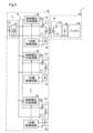
- FIG. 2 is a circuit diagram of a wireless power supply system
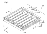
- FIG. 3 is a perspective view of a variable capacitor
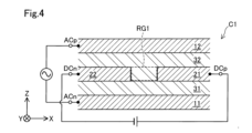
- FIG. 4 is a cross-sectional view of the variable capacitor shown in FIG. 3 taken along line IV-IV
- FIG. 5 is a diagram showing the relationship between the control electric field and the relative dielectric constant
- FIG. 6 is a circuit diagram of a power supply device
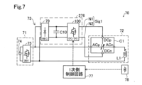
- FIG. 7 is a circuit diagram of a power supply device according to a second embodiment
- FIG. 8 is a circuit diagram of a power supply device according to a third embodiment
- FIG. 9 is a circuit diagram of a power supply device according to a fourth embodiment
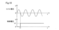
- FIG. 10 is a diagram showing the relationship between the start timing of application of the control voltage and the coil voltage
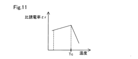
- FIG. 11 is a diagram showing the dielectric characteristics of the dielectric layer according to the fifth embodiment.
- the contactless power supply system 1 includes a power supply device 70 and a power receiving device 80.
- the power supply device 70 is buried under a road RS.
- the power receiving device 80 is mounted on a vehicle VE as a moving body that travels on the road RS.
- the power receiving device 80 is supplied with power from the power supply device 70.
- “traveling” includes a case where the vehicle VE is moving and a case where the vehicle is stopped, such as waiting at a traffic light.
- the vehicle VE is configured as, for example, an electric vehicle or a hybrid vehicle.
- the power supply device 70 has a primary side resonant circuit 72, which is a series resonant circuit having a primary side coil L1 and a variable capacitance capacitor C1, and an AC power source 71 that supplies power to the primary side resonant circuit 72.
- the AC power source 71 supplies power to the multiple primary side resonant circuits 72.
- the multiple primary side coils L1 are arranged along the extension direction of the road RS.
- the power receiving device 80 has a secondary side coil L2.
- the moving object on which the power receiving device 80 is mounted is not limited to a vehicle VE traveling on the road RS, but may be, for example, an AGV (automated guided vehicle) or a traveling robot.
- the power supply device 70 may be installed not under the road RS, but on a sidewalk or parking lot adjacent to the road RS, or on a route along which the AGV travels.
- the power supply device 70 includes a control circuit 73 and a primary side detection circuit 78.
- the control circuit 73 has a control voltage application circuit 76 and a primary side control circuit 77.
- a primary side coil L1 and a variable capacitance capacitor C1 are connected in series to configure a primary side resonant circuit 72 as a resonant circuit.
- the control circuit 73 controls the operation of the power supply device 70 by adjusting the electric field applied between the first control electrode layer 21 and the second control electrode layer 22 to adjust the capacitance value of the electrostatic capacitance stored between the first extraction electrode layer 11 and the second control electrode layer 22.
- the control voltage application circuit 76 applies a control voltage between the first control electrode layer 21 and the second control electrode layer 22.
- the control voltage is a voltage for changing the dielectric constant of the second dielectric layer 32.
- the variable capacitance capacitor C1 adjusts the resonant frequency of the primary side resonant circuit 72 by adjusting its capacitance value using the control voltage.
- the AC power supply 71 has a DC power supply 74 and an inverter 75.
- the inverter 75 converts the DC power supplied from the DC power supply 74 into AC power of a predetermined operating frequency and applies it to the primary side resonant circuit 72.
- the operating frequency is 85 kHz.
- the variable capacitance capacitor C1 has a function of putting the primary side resonant circuit 72 in a resonant state at the operating frequency and putting the primary side resonant circuit 72 in a non-resonant state at the operating frequency.
- the variable capacitance capacitor C1 is configured to be switchable between a first capacitance value and a second capacitance value smaller than the first capacitance value.
- the capacitance value of the variable capacitance capacitor C1 is switched between the first capacitance value and the second capacitance value by a switching signal Sig1 output from the control voltage application circuit 76.
- the primary side resonant circuit 72 is in a resonant state at the operating frequency.
- the first capacitance value of the variable capacitor C1 is set to a value that makes the resonant frequency of the primary side resonant circuit 72 match the operating frequency.
- variable capacitor C1 has the second capacitance value
- the resonant frequency of the primary side resonant circuit 72 deviates from the operating frequency, so the primary side resonant circuit 72 is in a non-resonant state at the operating frequency.
- the control voltage application circuit 76 applies a switching signal Sig1 generated using AC power output from the AC power supply 71 to the variable capacitor C1.
- the primary side detection circuit 78 is a magnetic sensor that detects the magnitude of the magnetic flux near the primary side coil L1, more specifically, a magnetic sensor with a built-in coil provided near the primary side coil L1.
- the primary side detection circuit 78 detects the magnetic flux density and outputs a signal indicating the detected magnetic flux density to the primary side control circuit 77.
- the primary side control circuit 77 uses the signal output from the primary side detection circuit 78 to instruct the control voltage application circuit 76 to switch the voltage value of the switching signal Sig1 to the variable capacitance capacitor C1. Specifically, when the magnetic flux density indicated by the signal is greater than a predetermined threshold value, the primary side control circuit 77 instructs the control voltage application circuit 76 to switch the voltage value of the switching signal Sig1 to the variable capacitance capacitor C1.
- the power receiving device 80 has a secondary resonant circuit 81, a rectifier 82, and a battery 83.
- the secondary coil L2 and the secondary capacitor C2 are connected in series to form the secondary resonant circuit 81.
- the rectifier 82 converts the AC power output from the secondary resonant circuit 81 into DC power and supplies it to the battery 83.
- the battery 83 is charged by the supplied DC power.
- the resonant frequency of the primary resonant circuit 72 and the resonant frequency of the secondary resonant circuit 81 are set to be substantially the same. This allows contactless power supply to the power receiving device 80 through magnetic field resonance between the primary coil L1 and the secondary coil L2.
- a state in which the variable capacitor C1 is set to a first capacitance value, a power transmission current flows through the primary coil L1, and power is being supplied is called a power supply state.
- a state in which the variable capacitor C1 is set to a second capacitance value, a standby current smaller than the power transmission current flows through the primary coil L1, and power is not being supplied is called a standby state.
- the primary coil L1 is arranged in the direction in which the road RS extends, and the secondary coil L2 receives contactless power from the nearest primary coil L1.
- a standby current flows through the primary coil L1, causing the primary coil L1 to generate magnetic flux.
- the power receiving device 80 is equipped with a magnetic sensor (not shown). When the power receiving device 80 approaches the target primary resonant circuit 72, the magnetic sensor detects the magnetic flux generated by the primary coil L1. When the power receiving device 80 detects the magnetic flux, it passes an AC current through the secondary coil L2 to generate magnetic flux. When the magnetic flux generated by the secondary coil L2 is detected by the primary detection circuit 78, the primary control circuit 77 commands the control voltage application circuit 76 to switch the voltage value of the switching signal Sig1.
- variable capacitance capacitor C1 switches the capacitance value from the second capacitance value to the first capacitance value using the voltage value of the switching signal Sig1. This causes the primary side resonant circuit 72 to enter a resonant state and power supply begins.
- the power supply device 70 detects the presence of the secondary coil L2 is not limited to the above. In other embodiments, the power supply device 70 may detect the current flowing through the primary coil L1 and detect an increase in the current, or detect the voltage of the primary coil L1 and detect an increase in the voltage.
- variable capacitance capacitor C1 has a first extraction electrode layer 11, a second extraction electrode layer 12, a first control electrode layer 21, a second control electrode layer 22, a first dielectric layer 31, a second dielectric layer 32, a first extraction electrode common layer 41, and a second extraction electrode common layer 42.
- the first extraction electrode layer 11 and the second extraction electrode layer 12 are also collectively referred to as the extraction electrode layer 10.
- the first control electrode layer 21 and the second control electrode layer 22 are also collectively referred to as the control electrode layer 20.
- the XYZ axes are drawn, which are three mutually orthogonal spatial axes.
- the directions in which the X, Y, and Z arrows point indicate the positive directions along the X, Y, and Z axes, respectively.
- the positive directions along the X, Y, and Z axes are the +X, +Y, and +Z directions, respectively.
- the directions opposite to the directions in which the X, Y, and Z arrows point are the negative directions along the X, Y, and Z axes, respectively.
- the negative directions along the X, Y, and Z axes are the -X, -Y, and -Z directions, respectively.
- the directions along the X, Y, and Z axes, regardless of whether they are positive or negative, are called the X direction, Y direction, and Z direction, respectively. The same applies to the figures and explanations shown below.
- the first control electrode layer 21 and the second control electrode layer 22 are electrode layers for adjusting the capacitance of the variable capacitor C1.
- the first extraction electrode layer 11 and the second extraction electrode layer 12 are electrode layers for utilizing the capacitance of the variable capacitor C1.
- the variable capacitor C1 is used by applying a control voltage, which is a DC voltage, to the first control electrode layer 21 and the second control electrode layer 22, and applying AC power between the first extraction electrode layer 11 and the second extraction electrode layer 12.
- the variable capacitor C1 further has a first terminal ACp, a second terminal ACn, a third terminal DCp, and a fourth terminal DCn for electrically connecting to an external circuit.
- the first terminal ACp is electrically connected to the first extraction electrode layer 11.
- the second terminal ACn is electrically connected to the second extraction electrode layer 12.
- the third terminal DCp is electrically connected to the first control electrode layer 21.
- the fourth terminal DCn is electrically connected to the second control electrode layer 22.
- the second control electrode layer 22 faces the first control electrode layer 21.
- the second dielectric layer 32 is disposed at least between the first control electrode layer 21 and the second control electrode layer 22.
- the first extraction electrode layer 11 and the second extraction electrode layer 12 face each other with the second dielectric layer 32 in between.
- the first extraction electrode layer 11 and the second extraction electrode layer 12 are disposed at positions that generate an electric field along a direction intersecting with the electric field vector generated between the first control electrode layer 21 and the second control electrode layer 22 when a control voltage is applied between the first control electrode layer 21 and the second control electrode layer 22.
- the first control electrode layer 21 and the second control electrode layer 22 face each other in the X direction.
- the first extraction electrode layer 11 and the second extraction electrode layer 12 face each other in the Z direction.
- the variable capacitor C1 has a layered structure. Specifically, a first dielectric layer 31 is disposed on the first extraction electrode layer 11. A first control electrode layer 21, a second control electrode layer 22, and a second dielectric layer 32 are disposed on the first dielectric layer 31. The second dielectric layer 32 covers the first control electrode layer 21 and the second control electrode layer 22. A second extraction electrode layer 12 is disposed on the second dielectric layer 32.
- the film surface direction of each layer is the XY direction.
- the stacking direction in which each layer is stacked is the Z direction.
- the first control electrode layer 21 and the second control electrode layer 22 each have a flat plate shape with the long axis in the Y direction.
- the first control electrode layer 21 and the second control electrode layer 22 are alternately arranged at intervals in the X direction.
- the -Y direction end of each first control electrode layer 21 is electrically connected to the first extraction electrode common layer 41.
- the +Y direction end of each second control electrode layer 22 is electrically connected to the second extraction electrode common layer 42.
- the structure formed by alternately arranging the first control electrode layer 21 and the second control electrode layer 22 with the second dielectric layer 32 in between in the X direction is also referred to as the first structure ST1.
- the capacitors formed between the first control electrode layer 21 and the second control electrode layer 22 are connected in parallel with each other, so that the capacitance value of the variable capacitor C1 can be increased.
- the second dielectric layer 32 is disposed at least between the first control electrode layer 21 and the second control electrode layer 22. Specifically, the second dielectric layer 32 is disposed in a control region RG1 sandwiched between the first control electrode layer 21 and the second control electrode layer 22 in the X direction.
- a control voltage which is a DC voltage
- an electric field vector that is approximately parallel to the X direction is generated in the control region RG1.
- the first extraction electrode layer 11 and the second extraction electrode layer 12 face each other in the Z direction, sandwiching the second dielectric layer 32.
- the electric field vector generated in the control region RG1 when an AC voltage is applied between the first extraction electrode layer 11 and the second extraction electrode layer 12 roughly intersects with the voltage vector generated in the control region RG1 when a control voltage is applied between the first control electrode layer 21 and the second control electrode layer 22.
- the electric field vector generated in the control region RG1 when an AC voltage is applied between the first extraction electrode layer 11 and the second extraction electrode layer 12 roughly intersects with the voltage vector generated in the control region RG1 when a control voltage is applied between the first control electrode layer 21 and the second control electrode layer 22.
- the direction in which the first extraction electrode layer 11 and the second extraction electrode layer 12 face each other is different from the direction in which the first control electrode layer 21 and the second control electrode layer 22 face each other. This allows the distance between the first extraction electrode layer 11 and the second extraction electrode layer 12 and the distance between the first control electrode layer 21 and the second control electrode layer 22 to be set independently. The distance between the first control electrode layer 21 and the second control electrode layer 22 can be shortened without shortening the distance between the first extraction electrode layer 11 and the second extraction electrode layer 12.
- the electric field applied between the first control electrode layer 21 and the second control electrode layer 22 can be increased. Therefore, the control voltage can be reduced.
- the first dielectric layer 31 and the second dielectric layer 32 contain a ferroelectric material of the same material.
- the first dielectric layer 31 and the second dielectric layer 32 contain PVDF (polyvinylidene fluoride).
- the first dielectric layer 31 and the second dielectric layer 32 may contain a ferroelectric polymer such as a fluororesin such as P(VDF-TrFE) (poly(vinylidene fluoride-trifluoroethylene)).
- a ferroelectric polymer such as a fluororesin such as P(VDF-TrFE) (poly(vinylidene fluoride-trifluoroethylene)).
- the first dielectric layer 31 and the second dielectric layer 32 may include dielectrics of different materials.
- PVDF molecules have hydrogen atoms and fluorine atoms bonded to the carbon chain. Hydrogen atoms are positively charged and fluorine atoms are negatively charged, so PVDF molecules have a dipole moment. When PVDF molecules aggregate due to intermolecular forces, the carbon chains of each PVDF molecule extend in the same direction. Hydrogen atoms and fluorine atoms are located perpendicular to the direction in which the carbon chains extend. Therefore, PVDF crystals are spontaneously polarized. When an electric field is applied to a PVDF crystal, the direction of polarization changes so that the crystal rotates around the X-axis, which is the direction in which the carbon chains extend, as the central axis.
- FIG. 5 shows the relationship between the magnitude of the control electric field Ed generated by applying a control voltage between the first control electrode layer 21 and the second control electrode layer 22, and the relative dielectric constant ⁇ r when an AC voltage is applied between the first extraction electrode layer 11 and the second extraction electrode layer 12.
- the variable capacitor C1 has dielectric characteristics in which the relative dielectric constant ⁇ r has two peaks.
- Ferroelectrics are spontaneously polarized when the control electric field is zero V/m.
- the control electric field is increased to the coercive electric field Ec, the polarization becomes zero and the relative dielectric constant ⁇ r becomes maximum.
- the dipole moment tends to move in a direction corresponding to the AC voltage applied between the first extraction electrode layer 11 and the second extraction electrode layer 12, so it is thought that the relative dielectric constant ⁇ r becomes large.
- the direction of the control electric field Ed and the direction of the electric field caused by the application of an AC voltage intersect.
- the PVDF contained in the second dielectric layer 32 has a polarization direction that rotates around the carbon chain as the axis of rotation. For this reason, even in regions where the control electric field Ed is smaller than the coercive electric field Ec, a peak in the relative dielectric constant ⁇ r appears. This is thought to be because the application of the control electric field Ed makes it easier for the electric dipoles to move in response to the application of an AC voltage than when the control electric field Ed is not applied.
- the dielectric characteristics of the variable capacitor C1 have an assist region, a polarization inversion region, and a saturation region.
- the assist region is a region where the control electric field Ed is smaller than the coercive electric field Ec, and the relative dielectric constant ⁇ r is larger than the relative dielectric constant ⁇ 1 and smaller than the relative dielectric constant ⁇ 2.
- the relative dielectric constant ⁇ 1 is the relative dielectric constant ⁇ r when the control electric field Ed is zero.
- the relative dielectric constant ⁇ 2 is the minimum point between the two peaks of the relative dielectric constant ⁇ r.
- the polarization inversion region is an electric field range in which the control electric field Ed includes the coercive electric field Ec, and is a region in which the relative dielectric constant ⁇ r is greater than the peak value ⁇ 3 of the relative dielectric constant ⁇ r in the assist region.
- the saturation region is a region in which the control electric field Ed is greater than the coercive electric field Ec, and the control electric field Ed is greater than the coercive electric field Ec.
- the control electric field Ed in the assist region As described above, by applying the control electric field Ed in the assist region, the polarization can be made to move more easily than when the control electric field Ed is not applied. Therefore, by applying the control electric field Ed in the assist region to the variable capacitor C1, the capacitance of the variable capacitor C1 can be made larger than the capacitance when the control electric field Ed is not applied.
- the polarization can be made to move more easily than in the assist region. Therefore, by applying a control electric field Ed in the polarization inversion region to the variable capacitor C1, the capacitance of the variable capacitor C1 can be made larger than the capacitance when a control electric field Ed in the assist region is applied.
- the capacitance of the variable capacitor C1 can be made smaller than the capacitance when the control electric field Ed in the assist region is not applied.
- the capacitance value of the variable capacitor C1 can be set to a desired capacitance value by adjusting the magnitude of the control electric field Ed.
- the control voltage application circuit 76 includes a rectifier 79, a smoothing capacitor C10, and a switch SW.
- the rectifier 79 rectifies the AC current output from the AC power supply 71, and outputs a DC voltage to the wiring N1 and the wiring N2.
- a diode bridge circuit can be used as the rectifier 79.
- the voltage applied to the wiring N1 is higher than the voltage applied to the wiring N2.
- the switch SW is disposed on the wiring N1.
- the switch SW is, for example, a transistor.
- the smoothing capacitor C10 is connected between the wiring N1 and the wiring N2.
- the switching signal Sig1 is specifically the voltage between the wiring N1 and the wiring N2.
- Wiring N1 is connected to the third terminal DCp of the variable capacitor C1.
- Wiring N2 is connected to the fourth terminal DCn of the variable capacitor C1.
- the wiring connected to one output terminal of the inverter 75 is connected to the first terminal ACp of the variable capacitor C1.
- the wiring connected to the other output terminal of the inverter 75 is connected to the second terminal ACn of the variable capacitor C1.
- the primary side control circuit 77 outputs a signal to the control voltage application circuit 76 to set the switch SW to an open state or a conductive state. Specifically, when the power supply device 70 is set to a power supply state, the primary side control circuit 77 outputs a signal to set the switch SW to an open state. When a signal is input from the primary side control circuit 77, the control voltage application circuit 76 performs a supply operation to set the switch SW to an open state. In the supply operation, the control voltage application circuit 76 sets the control voltage to zero volts as the first control voltage. As a result, the control voltage Vd applied between the first control electrode layer 21 and the second control electrode layer 22 of the variable capacitance capacitor C1 becomes zero volts.
- the capacitance value of the variable capacitance capacitor C1 is set to the first capacitance value when the relative dielectric constant ⁇ r of the second dielectric layer 32 is the relative dielectric constant ⁇ 1. Therefore, the primary side resonant circuit 72 is in a resonant state.
- the primary side control circuit 77 when the power supply device 70 is set to a standby state, the primary side control circuit 77 outputs a signal to set the switch SW to a conductive state.
- the control voltage application circuit 76 receives a signal from the primary side control circuit 77, it performs a standby operation to set the switch SW to a conductive state.
- the control voltage application circuit 76 sets the control voltage to a voltage value that becomes the control electric field Ed in the saturation region as the second control voltage.
- the control electric field Ed applied between the first control electrode layer 21 and the second control electrode layer 22 of the variable capacitance capacitor C1 becomes an electric field in the saturation region.
- the capacitance value of the variable capacitance capacitor C1 is set to the second capacitance value when the relative dielectric constant ⁇ r in the saturation region of the second dielectric layer 32 is set. As described above, the second capacitance value is smaller than the first capacitance value. As a result, the primary side resonant circuit 72 is in a non-resonant state.
- the first extraction electrode layer 11 and the second extraction electrode layer 12 are arranged at positions that generate an electric field along a direction intersecting with the electric field vector generated when the control voltage is applied. This allows the distance between the first extraction electrode layer 11 and the second extraction electrode layer 12 and the distance between the first control electrode layer 21 and the second control electrode layer 22 to be set independently. This allows the control voltage to be reduced.
- variable capacitance capacitor C1 is used in the control voltage application circuit 76 that adjusts the control electric field Ed applied between the first control electrode layer 21 and the second control electrode layer 22 in the non-contact power supply system 1, and adjusts the capacitance value of the electrostatic capacitance stored between the first extraction electrode layer 11 and the second control electrode layer 22 to control the operation of the non-contact power supply system 1.
- This allows the circuit size to be reduced compared to a case where the circuit is configured with multiple capacitors and switches to change the capacitance value of the capacitance component of the primary side resonant circuit 72.
- the circuit can be made smaller than a capacitor whose capacitance value is changed mechanically.
- variable capacitor C1 is also used to adjust the resonant frequency of the primary resonant circuit 72 and control the operation of the primary resonant circuit 72. This allows the circuit size to be smaller than a circuit configuration that has multiple capacitors to change the capacitance value of the capacitance component of the primary resonant circuit 72.
- the control voltage application circuit 76 also executes a power supply operation in which the primary resonant circuit 72 is set to a resonant state by setting the control voltage Vd to zero volts, and a standby operation in which the primary resonant circuit 72 is set to a non-resonant state by setting the control voltage to a voltage in the saturation region.
- the variable capacitance capacitor C1 is set to a first capacitance value by setting the control voltage Vd to zero volts, and is set to a second capacitance value by setting the control voltage Vd to the voltage value of the control electric field Ed in the saturation region.
- a power supply device 70 that uses magnetic field resonance to supply power non-contact, whether or not the power supply device is to supply power can be controlled by setting the primary resonant circuit 72 to a resonant state or a non-resonant state.
- the variable capacitance capacitor C1 according to this embodiment can be suitably applied to such a power supply device 70.
- the second capacitance value is smaller than the first capacitance value. This allows the impedance of the primary resonant circuit 72 to be reduced when the contactless power supply system 1 is in a standby state, thereby reducing the current flowing through the primary coil L1.
- a power supply device 70 according to the second embodiment differs from the first embodiment in the configuration of a control voltage application circuit 276.
- the same components as those in the above embodiment are denoted by the same reference numerals, and detailed description thereof will be omitted as appropriate.
- the control voltage application circuit 276 has a rectifier 79, a smoothing capacitor C10, and a DC-DC converter 100.
- the DC-DC converter 100 steps down or steps up the DC voltage output from the rectifier 79, and outputs it to wiring N1 and wiring N2.
- the control voltage output by the control voltage application circuit 276 is the same as in the first embodiment.
- the control voltage application circuit 276 outputs a voltage that is linear with respect to time. This suppresses sudden fluctuations in current, thereby making it possible to suppress surge voltages.
- a power supply device 70 according to the third embodiment differs from the above-described embodiments in the configuration of a control voltage application circuit 376.
- the same components as those in the above-described embodiments are denoted by the same reference numerals, and detailed description thereof will be omitted as appropriate.
- the control voltage application circuit 376 has a capacitor C30, a first diode D1, a second diode D2, a smoothing capacitor C10, and a DC-DC converter 100.
- a half-wave voltage doubler rectifier circuit is formed by the capacitor C30, the first diode D1, the second diode D2, and the smoothing capacitor C10. This makes it possible to output a large control voltage Vd.
- the control voltage output by the control voltage application circuit 376 is the same as in the first embodiment.
- a power supply device 70 according to the fourth embodiment differs from the above-described embodiments in the configuration of a control voltage application circuit 476.
- the same components as those in the above-described embodiments are denoted by the same reference numerals, and detailed description thereof will be omitted as appropriate.
- the control voltage application circuit 476 is connected to both terminals of the primary coil L1.
- the control voltage application circuit 476 converts the coil voltage, which is an AC voltage applied to the primary coil L1, into a DC voltage and supplies it to the wiring N1 and the wiring N2.
- the control voltage application circuit 476 when switching from power supply operation to standby operation, starts the standby operation from about time t1 when the coil voltage is zero volts. Specifically, the control voltage application circuit 476 starts applying the control voltage Vd in the saturation region between the third terminal DCp and the fourth terminal DCn from about time t1.
- “about time t1” refers to the period around time t1 when the voltage of the AC power is 10% or less of the maximum voltage value of the AC power.
- the control voltage application circuit 476 performs standby operation from time t1.
- control electric field Ed is applied to the second dielectric layer 32 of the variable capacitor C1 in a state where the second dielectric layer 32 is not easily affected by the electric field caused by the application of AC power, so that the control electric field can be effectively applied to the second dielectric layer 32.
- the control voltage is applied to the variable capacitor C1 when the voltage of the AC power applied to the primary coil L1 approaches zero volts.
- the control electric field Ed is applied to the second dielectric layer 32 in a state where it is not easily affected by the electric field caused by the application of AC power, so that the control electric field can be effectively applied to the second dielectric layer 32.
- the second dielectric layer 32 has a dielectric characteristic in which the relative dielectric constant ⁇ r at a temperature higher than the phase transition temperature Tc as the operating temperature is smaller than the relative dielectric constant ⁇ r at the phase transition temperature Tc. Specifically, when the temperature of the second dielectric layer 32 becomes higher than the phase transition temperature Tc, the relative dielectric constant ⁇ r decreases.
- the dielectric used for the second dielectric layer 32 is manufactured so that the phase transition temperature Tc is a value smaller than the operating temperature when the power supply device 70 is in an abnormal state. As a result, when the control circuit 73 becomes abnormally high temperature, the capacitance value of the variable capacitance capacitor C1 decreases. Therefore, it becomes difficult for a current to flow through the primary side resonant circuit 72, and the primary side resonant circuit 72 can be protected.
- the second dielectric layer 32 has a dielectric characteristic in which the relative dielectric constant ⁇ r decreases at temperatures higher than the phase transition temperature Tc.
- the capacitance value of the variable capacitor C1 decreases, so that the current flowing through the primary coil L1 can be reduced to protect the primary resonant circuit 72.
- the second dielectric layer 32 includes a ferroelectric polymer.
- the second dielectric layer 32 may include an inorganic ferroelectric such as barium titanate (BaTiO 3 ).
- the relative dielectric constant ⁇ r of an inorganic ferroelectric also changes depending on the magnitude of the control voltage. For this reason, it can be used as the dielectric layer of the variable capacitance capacitor C1. It is even better if the inorganic ferroelectric is polarized in multiple directions. This is because, even when the direction in which the control voltage is applied is different from the direction in which the AC voltage is applied, the relative dielectric constant changes depending on the magnitude of the control voltage, so that a variable capacitance capacitor C1 with a good variability can be provided.
- control voltage application circuit 76 applies a control voltage in the saturation region when the power supply device 70 is in a standby state, and does not apply a control voltage when the power supply device 70 is in a power transmission state.
- the control voltage application circuit 76 may apply a control voltage in the polarization inversion region or the assist region when the power supply device 70 is in a standby state, and may not apply a control voltage when the power supply device 70 is in a power transmission state.
- the primary resonant circuit 72 has a variable capacitor C1 connected in series to the primary coil L1
- the secondary resonant circuit 81 has a secondary capacitor C2 connected in series to the secondary coil L2, which is a so-called S-S type circuit configuration.
- the circuit configuration of the primary resonant circuit 72 and the circuit configuration of the secondary resonant circuit 81 are not limited to the S-S type.
- the primary resonant circuit 72 may have a variable capacitor C1 connected in parallel to the primary coil L1
- the secondary resonant circuit 81 may have a so-called P-S type circuit configuration, in which the secondary capacitor C2 is connected in series to the secondary coil L2.
- the secondary resonant circuit 81 may have a so-called P-SS type circuit configuration in which two secondary capacitors C2 are connected in series to both terminals of the secondary coil L2.
- the primary resonant circuit 72 may have a closed circuit in which a coil and a capacitor are connected in series. The coil of this closed circuit is arranged in a position where it can be magnetically coupled to the secondary coil L2 when the primary coil L1 and the secondary coil L2 are magnetically coupled.
- the capacitor of the closed circuit may be connected in parallel to the coil instead of in series.
- the primary resonant circuit 72 may have a coil connected in series to the primary coil L1 and a capacitor connected in parallel to the coil. The coil is arranged in a position where it can be magnetically coupled to the secondary coil L2 when the primary coil L1 and the secondary coil L2 are magnetically coupled.
- variable capacitor C1 is applied to the power supply device 70.
- the device to which the variable capacitor C1 is applied is not limited to the power supply device 70.
- the variable capacitor C1 can be used in a device that includes a circuit for converting frequencies.
- the variable capacitor according to claim 1 The device further includes a resonant circuit (72) formed of the variable capacitor and a primary coil (L1), the control circuit further includes a control voltage application circuit (76, 276, 376, 476) that applies a control voltage between the first control electrode layer and the second control electrode layer to change the dielectric constant of the dielectric layer; The variable capacitor adjusts a capacitance value using the control voltage, thereby adjusting a resonant frequency of the resonant circuit.
- a variable capacitance capacitor according to aspect 2, the device is a power supply device that wirelessly supplies power to a power receiving device,
- the control voltage application circuit includes: a power supply operation of setting the control voltage to a first control voltage to set the resonant circuit in a resonant state when AC power having a predetermined operating frequency is applied to the resonant circuit; a standby operation of setting the resonant circuit to a non-resonant state when the AC power of the operating frequency is applied to the resonant circuit by setting the control voltage to a second control voltage different from the first control voltage;
- the variable capacitor is set to a first capacitance value when the first control voltage is applied, and is set to a second capacitance value different from the first capacitance value when the second control voltage is applied.
- a variable capacitance capacitor according to aspect 3 is a series resonant circuit, The second capacitance value is smaller than the first capacitance value.
- a variable capacitance capacitor according to aspect 3 or 4 A variable capacitor, in which application of the second control voltage begins from approximately the time point when the voltage of the AC power applied to the primary coil is zero volts.
- (Form 6) 6. The variable capacitor according to any one of aspects 1 to 5, A variable capacitor, wherein the dielectric layer has a dielectric characteristic in which the relative dielectric constant at a temperature higher than a predetermined operating temperature is smaller than the relative dielectric constant at the operating temperature.
- the variable capacitor is A first control electrode layer (21); a second control electrode layer (22) facing the first control electrode layer; a dielectric layer (32) disposed at least between the first control electrode layer and the second control electrode layer; a first extracting electrode layer (11) and a second extracting electrode layer (12) facing each other with the dielectric layer interposed therebetween; the first extraction electrode layer and the second extraction electrode layer are disposed at positions that generate an electric field along a direction intersecting an electric field vector generated between the first control electrode layer and the second control electrode layer when the control voltage is applied between the first control electrode layer and the second control electrode layer,
- the control voltage application circuit includes: a power supply operation of setting the control voltage to a first control voltage and setting the variable capacitor to a first capacitance
- control circuit and the method described in the present disclosure may be realized by a dedicated computer provided by configuring a processor and a memory programmed to execute one or more functions embodied in a computer program.
- control circuit and the method described in the present disclosure may be realized by a dedicated computer provided by configuring a processor with one or more dedicated hardware logic circuits.
- control unit and the method described in the present disclosure may be realized by one or more dedicated computers configured by combining a processor and a memory programmed to execute one or more functions with a processor configured with one or more hardware logic circuits.
- the computer program may be stored in a computer-readable non-transient tangible recording medium as instructions executed by the computer.
Landscapes
- Engineering & Computer Science (AREA)
- Power Engineering (AREA)
- Microelectronics & Electronic Packaging (AREA)
- Computer Networks & Wireless Communication (AREA)
- Manufacturing & Machinery (AREA)
- Filters And Equalizers (AREA)
- Fixed Capacitors And Capacitor Manufacturing Machines (AREA)
- Charge And Discharge Circuits For Batteries Or The Like (AREA)
Abstract
Description
A1.非接触給電システムの構成:
図1に示すように、非接触給電システム1は、給電装置70と、受電装置80とを備える。本実施形態では、給電装置70は、道路RSの下に埋設されている。受電装置80は、道路RSを走行する移動体としての車両VEに搭載されている。車両VEの走行中に、受電装置80は、給電装置70から給電される。ここで、走行中とは、車両VEが移動している場合と、信号待ち等で車両が停止している場合とを含む。車両VEは、例えば、電気自動車やハイブリッド車として構成される。
図2に示すように、給電装置70は、上記構成に加え、制御回路73と、1次側検出回路78とを備えている。制御回路73は、制御電圧印加回路76と、1次側制御回路77とを有する。1次側コイルL1と可変容量コンデンサC1とが直列に接続されて、共振回路としての1次側共振回路72が構成されている。
可変容量コンデンサC1が第1容量値に設定され、1次側コイルL1に送電電流が流れて、給電が行われている状態を給電状態と呼ぶ。可変容量コンデンサC1が第2容量値に設定され、1次側コイルL1に送電電流よりも小さい待機電流が流れて、給電を行っていない状態を待機状態と呼ぶ。
図3に示すように、可変容量コンデンサC1は、第1取出電極層11と、第2取出電極層12と、第1制御電極層21と、第2制御電極層22と、第1誘電体層31と、第2誘電体層32と、第1取出電極共通層41と、第2取出電極共通層42とを有する。第1取出電極層11と第2取出電極層12とを総称して取出電極層10とも呼ぶ。第1制御電極層21と第2制御電極層22とを総称して制御電極層20とも呼ぶ。
図6に示すように、制御電圧印加回路76は、整流器79と、平滑コンデンサC10と、スイッチSWとを有する。整流器79は、交流電源71から出力される交流電流を整流し、配線N1と配線N2とに直流電圧を出力する。整流器79として、例えばダイオードブリッジ回路を用いることができる。配線N1に印加される電圧は、配線N2に印加される電圧よりも高い。配線N1に、スイッチSWが配置されている。スイッチSWは例えばトランジスタである。配線N1と配線N2との間に平滑コンデンサC10が接続されている。切替信号Sig1は、具体的には、配線N1と配線N2間の電圧である。
図7に示す、第2実施形態に係る給電装置70は、第1実施形態と制御電圧印加回路276の構成が異なる。上記実施形態と同じ構成については、同一の符号を付し、詳細な説明は適宜省略する。
図8に示す、第3実施形態に係る給電装置70は、上記各実施形態と制御電圧印加回路376の構成が異なる。上記実施形態と同じ構成については、同一の符号を付し、詳細な説明は適宜省略する。
図9に示す、第4実施形態に係る給電装置70は、上記各実施形態と制御電圧印加回路476の構成が異なる。上記実施形態と同じ構成については、同一の符号を付し、詳細な説明は適宜省略する。
図11に示すように、本実施形態では第2誘電体層32は、動作温度としての相転移温度Tcより高い温度における比誘電率εrが、相転移温度Tcにおける比誘電率εrよりも小さい誘電特性を有する。具体的には、第2誘電体層32は、相転移温度Tcより温度が高くなると、比誘電率εrが低下する。本実施形態では、相転移温度Tcは、給電装置70が異常状態となった場合の動作温度より小さい値となるように、第2誘電体層32に用いられる誘電体が作製されている。これにより、制御回路73が異常により高温となった場合に、可変容量コンデンサC1の容量値が低下する。このため、1次側共振回路72に電流が流れにくくなり、1次側共振回路72を保護することができる。
(F1)上記第1実施形態では、第2誘電体層32は、強誘電体ポリマーを含む。他の実施形態として、第2誘電体層32は、例えば、チタン酸バリウム(BaTiO3)などの無機強誘電体を含んでもよい。無機強誘電体でも、制御電圧の大きさに応じて、比誘電率εrが変化する。このため、可変容量コンデンサC1の誘電体層として用いることができる。複数の方向に分極する無機強誘電体であるとさらによい。制御電圧が印加される方向と、交流電圧が印加される方向が異なる場合にも、制御電圧の大きさにより比誘電率が変化するため、良好な可変率を有する可変容量コンデンサC1を提供することができるからである。
本開示の特徴を以下の通り示す。
(形態1)
装置(70)の動作を制御する制御回路(73)に用いられる可変容量コンデンサ(C1)であって、
第1制御電極層(21)と、
前記第1制御電極層と向かい合う第2制御電極層(22)と、
少なくとも、前記第1制御電極層と前記第2制御電極層との間に配置された誘電体層(32)と、
前記誘電体層を挟んで向かい合う第1取出電極層(11)と、第2取出電極層(12)とを備え、
前記第1取出電極層と前記第2取出電極層とは、前記第1制御電極層と前記第2制御電極層との間に電圧が印加された場合に、前記第1制御電極層と前記第2制御電極層との間に生じる電界ベクトルと交わる方向に沿って電界を生じさせる位置に配置されており、
前記第1制御電極層と前記第2制御電極層との間に印加される電圧が調整されて、前記第1取出電極層と前記第2制御電極層との間に蓄えられる静電容量の容量値が調整される、可変容量コンデンサ。
(形態2)
形態1に記載の可変容量コンデンサであって、
前記装置は、前記可変容量コンデンサと1次側コイル(L1)とで構成される共振回路(72)をさらに有し、
前記制御回路は、前記第1制御電極層と前記第2制御電極層との間に前記誘電体層の誘電率を変化させるための制御電圧を印加する制御電圧印加回路(76,276,376,476)をさらに有し、
前記可変容量コンデンサは、前記制御電圧を用いて容量値を調整することにより、前記共振回路の共振周波数を調整する、可変容量コンデンサ。
(形態3)
形態2に記載の可変容量コンデンサであって、
前記装置は、受電装置に非接触給電する給電装置であり、
前記制御電圧印加回路は、
前記制御電圧を第1制御電圧に設定することにより、前記共振回路に予め定められた動作周波数の交流電力が印加された場合に、前記共振回路を共振状態に設定する給電動作と、
前記制御電圧を前記第1制御電圧とは異なる第2制御電圧に設定することにより、前記共振回路に前記動作周波数の前記交流電力が印加された場合に、前記共振回路を非共振状態に設定する待機動作、とを実行可能であり、
前記可変容量コンデンサは、前記第1制御電圧が印加された場合に第1容量値に設定され、前記第2制御電圧が印加された場合に前記第1容量値とは異なる第2容量値に設定される、可変容量コンデンサ。
(形態4)
形態3に記載の可変容量コンデンサであって、
前記共振回路は、直列共振回路であり、
前記第2容量値は、前記第1容量値よりも小さい、可変容量コンデンサ。
(形態5)
形態3または4に記載の可変容量コンデンサであって、
前記1次側コイルに印加される交流電力の電圧がゼロボルトである時点付近から前記第2制御電圧の印加が開始される、可変容量コンデンサ。
(形態6)
形態1から5のいずれか一項に記載の可変容量コンデンサであって、
前記誘電体層は、予め定められた動作温度より高い温度における比誘電率が、前記動作温度における比誘電率よりも小さい誘電特性を有する、可変容量コンデンサ。
(形態7)
受電装置(80)に非接触給電する給電装置(70)であって、
可変容量コンデンサ(C1)と1次側コイル(L1)とで構成される共振回路(72)と、
前記可変容量コンデンサに制御電圧を印加する制御電圧印加回路(76)と、を備え、
前記可変容量コンデンサは、
第1制御電極層(21)と、
前記第1制御電極層と向かい合う第2制御電極層(22)と、
少なくとも、前記第1制御電極層と前記第2制御電極層との間に配置された誘電体層(32)と、
前記誘電体層を挟んで向かい合う第1取出電極層(11)と、第2取出電極層(12)とを備え、
前記第1取出電極層と前記第2取出電極層とは、前記第1制御電極層と前記第2制御電極層との間に前記制御電圧が印加された場合に、前記第1制御電極層と前記第2制御電極層との間に生じる電界ベクトルと交わる方向に沿って電界を生じさせる位置に配置されており、
前記制御電圧印加回路は、
前記制御電圧を第1制御電圧に設定して、前記可変容量コンデンサを第1容量値に設定することにより、前記共振回路に予め定められた動作周波数の交流電力が印加された場合に、前記共振回路を共振状態に設定する給電動作と、
前記制御電圧を前記第1制御電圧とは異なる前記第2制御電圧に設定して、前記可変容量コンデンサを前記第1容量値とは異なる第2容量値に設定することにより、前記共振回路に前記動作周波数の前記交流電力が印加された場合に、前記共振回路を非共振状態に設定する待機動作、とを実行可能である、給電装置。
Claims (7)
- 装置(70)の動作を制御する制御回路(73)に用いられる可変容量コンデンサ(C1)であって、
第1制御電極層(21)と、
前記第1制御電極層と向かい合う第2制御電極層(22)と、
少なくとも、前記第1制御電極層と前記第2制御電極層との間に配置された誘電体層(32)と、
前記誘電体層を挟んで向かい合う第1取出電極層(11)と、第2取出電極層(12)とを備え、
前記第1取出電極層と前記第2取出電極層とは、前記第1制御電極層と前記第2制御電極層との間に電圧が印加された場合に、前記第1制御電極層と前記第2制御電極層との間に生じる電界ベクトルと交わる方向に沿って電界を生じさせる位置に配置されており、
前記第1制御電極層と前記第2制御電極層との間に印加される電圧が調整されて、前記第1取出電極層と前記第2制御電極層との間に蓄えられる静電容量の容量値が調整される、可変容量コンデンサ。 - 請求項1に記載の可変容量コンデンサであって、
前記装置は、前記可変容量コンデンサと1次側コイル(L1)とで構成される共振回路(72)をさらに有し、
前記制御回路は、前記第1制御電極層と前記第2制御電極層との間に前記誘電体層の誘電率を変化させるための制御電圧を印加する制御電圧印加回路(76,276,376,476)をさらに有し、
前記可変容量コンデンサは、前記制御電圧を用いて容量値を調整することにより、前記共振回路の共振周波数を調整する、可変容量コンデンサ。 - 請求項2に記載の可変容量コンデンサであって、
前記装置は、受電装置に非接触給電する給電装置であり、
前記制御電圧印加回路は、
前記制御電圧を第1制御電圧に設定することにより、前記共振回路に予め定められた動作周波数の交流電力が印加された場合に、前記共振回路を共振状態に設定する給電動作と、
前記制御電圧を前記第1制御電圧とは異なる第2制御電圧に設定することにより、前記共振回路に前記動作周波数の前記交流電力が印加された場合に、前記共振回路を非共振状態に設定する待機動作、とを実行可能であり、
前記可変容量コンデンサは、前記第1制御電圧が印加された場合に第1容量値に設定され、前記第2制御電圧が印加された場合に前記第1容量値とは異なる第2容量値に設定される、可変容量コンデンサ。 - 請求項3に記載の可変容量コンデンサであって、
前記共振回路は、直列共振回路であり、
前記第2容量値は、前記第1容量値よりも小さい、可変容量コンデンサ。 - 請求項3または4に記載の可変容量コンデンサであって、
前記1次側コイルに印加される交流電力の電圧がゼロボルトである時点付近から前記第2制御電圧の印加が開始される、可変容量コンデンサ。 - 請求項1に記載の可変容量コンデンサであって、
前記誘電体層は、予め定められた動作温度より高い温度における比誘電率が、前記動作温度における比誘電率よりも小さい誘電特性を有する、可変容量コンデンサ。 - 受電装置(80)に非接触給電する給電装置(70)であって、
可変容量コンデンサ(C1)と1次側コイル(L1)とで構成される共振回路(72)と、
前記可変容量コンデンサに制御電圧を印加する制御電圧印加回路(76)と、を備え、
前記可変容量コンデンサは、
第1制御電極層(21)と、
前記第1制御電極層と向かい合う第2制御電極層(22)と、
少なくとも、前記第1制御電極層と前記第2制御電極層との間に配置された誘電体層(32)と、
前記誘電体層を挟んで向かい合う第1取出電極層(11)と、第2取出電極層(12)とを備え、
前記第1取出電極層と前記第2取出電極層とは、前記第1制御電極層と前記第2制御電極層との間に前記制御電圧が印加された場合に、前記第1制御電極層と前記第2制御電極層との間に生じる電界ベクトルと交わる方向に沿って電界を生じさせる位置に配置されており、
前記制御電圧印加回路は、
前記制御電圧を第1制御電圧に設定して、前記可変容量コンデンサを第1容量値に設定することにより、前記共振回路に予め定められた動作周波数の交流電力が印加された場合に、前記共振回路を共振状態に設定する給電動作と、
前記制御電圧を前記第1制御電圧とは異なる第2制御電圧に設定して、前記可変容量コンデンサを前記第1容量値とは異なる第2容量値に設定することにより、前記共振回路に前記動作周波数の前記交流電力が印加された場合に、前記共振回路を非共振状態に設定する待機動作、とを実行可能である、給電装置。
Priority Applications (2)
| Application Number | Priority Date | Filing Date | Title |
|---|---|---|---|
| CN202480010151.7A CN120642014A (zh) | 2023-02-02 | 2024-01-25 | 可变容量电容器和供电装置 |
| US19/219,482 US20250285812A1 (en) | 2023-02-02 | 2025-05-27 | Variable capacitor and power supply apparatus |
Applications Claiming Priority (2)
| Application Number | Priority Date | Filing Date | Title |
|---|---|---|---|
| JP2023014372A JP7718436B2 (ja) | 2023-02-02 | 2023-02-02 | 可変容量コンデンサおよび給電装置 |
| JP2023-014372 | 2023-02-02 |
Related Child Applications (1)
| Application Number | Title | Priority Date | Filing Date |
|---|---|---|---|
| US19/219,482 Continuation US20250285812A1 (en) | 2023-02-02 | 2025-05-27 | Variable capacitor and power supply apparatus |
Publications (1)
| Publication Number | Publication Date |
|---|---|
| WO2024162152A1 true WO2024162152A1 (ja) | 2024-08-08 |
Family
ID=92146326
Family Applications (1)
| Application Number | Title | Priority Date | Filing Date |
|---|---|---|---|
| PCT/JP2024/002138 Ceased WO2024162152A1 (ja) | 2023-02-02 | 2024-01-25 | 可変容量コンデンサおよび給電装置 |
Country Status (4)
| Country | Link |
|---|---|
| US (1) | US20250285812A1 (ja) |
| JP (1) | JP7718436B2 (ja) |
| CN (1) | CN120642014A (ja) |
| WO (1) | WO2024162152A1 (ja) |
Citations (3)
| Publication number | Priority date | Publication date | Assignee | Title |
|---|---|---|---|---|
| JP2009267165A (ja) * | 2008-04-25 | 2009-11-12 | Sony Corp | 可変容量素子及び、電子機器 |
| JP2011138544A (ja) * | 2011-03-14 | 2011-07-14 | Sony Corp | 可変容量素子及び共振回路 |
| WO2021014932A1 (ja) * | 2019-07-25 | 2021-01-28 | 株式会社デンソー | 非接触給電装置 |
-
2023
- 2023-02-02 JP JP2023014372A patent/JP7718436B2/ja active Active
-
2024
- 2024-01-25 CN CN202480010151.7A patent/CN120642014A/zh active Pending
- 2024-01-25 WO PCT/JP2024/002138 patent/WO2024162152A1/ja not_active Ceased
-
2025
- 2025-05-27 US US19/219,482 patent/US20250285812A1/en active Pending
Patent Citations (3)
| Publication number | Priority date | Publication date | Assignee | Title |
|---|---|---|---|---|
| JP2009267165A (ja) * | 2008-04-25 | 2009-11-12 | Sony Corp | 可変容量素子及び、電子機器 |
| JP2011138544A (ja) * | 2011-03-14 | 2011-07-14 | Sony Corp | 可変容量素子及び共振回路 |
| WO2021014932A1 (ja) * | 2019-07-25 | 2021-01-28 | 株式会社デンソー | 非接触給電装置 |
Also Published As
| Publication number | Publication date |
|---|---|
| US20250285812A1 (en) | 2025-09-11 |
| JP2024110046A (ja) | 2024-08-15 |
| JP7718436B2 (ja) | 2025-08-05 |
| CN120642014A (zh) | 2025-09-12 |
Similar Documents
| Publication | Publication Date | Title |
|---|---|---|
| US9275792B2 (en) | Power supply system, and fixed body and movable body therefor | |
| CN107112812B (zh) | 用于在dc电压源之间无线传输电力的装置和方法 | |
| JP4737253B2 (ja) | 非接触受信装置 | |
| JP5224295B2 (ja) | 非接触給電装置及び非接触給電方法 | |
| WO2016051484A1 (ja) | 非接触給電装置 | |
| JP5516824B2 (ja) | 電力伝送システム | |
| JP2013027129A (ja) | 給電側設備及び共鳴型非接触給電システム | |
| US9312778B2 (en) | Power supply device | |
| WO2014178345A1 (ja) | 給電システム及び共振回路 | |
| WO2012063570A1 (ja) | 非接触給電装置 | |
| WO2015087398A1 (ja) | 受電装置、給電システム | |
| US20180183272A1 (en) | Non-contact power feeding device and control method for the same | |
| JP6111625B2 (ja) | ワイヤレス電力伝送装置 | |
| US20180183271A1 (en) | Non-contact power feeding device | |
| WO2024162152A1 (ja) | 可変容量コンデンサおよび給電装置 | |
| WO2015104779A1 (ja) | 非接触給電装置及び非接触給電装置の始動方法 | |
| JP2009212168A (ja) | 可変容量素子、可変容量素子の調整方法、可変容量デバイス、及び電子機器 | |
| CN107546979B (zh) | 功率转换装置 | |
| WO2016017143A1 (ja) | 非接触給電装置及びそれを用いた非接触給電システム | |
| WO2024162153A1 (ja) | 可変容量コンデンサおよび給電装置 | |
| JP2011138544A (ja) | 可変容量素子及び共振回路 | |
| JP5601152B2 (ja) | ワイヤレス電力伝送システムおよび送電装置 | |
| WO2020203690A1 (ja) | 受電装置、移動体、および無線電力伝送システム | |
| WO2024009682A1 (ja) | 送電装置、プログラム | |
| CN113692362A (zh) | 受电装置、移动体、无线电力传输系统以及移动体系统 |
Legal Events
| Date | Code | Title | Description |
|---|---|---|---|
| 121 | Ep: the epo has been informed by wipo that ep was designated in this application |
Ref document number: 24750101 Country of ref document: EP Kind code of ref document: A1 |
|
| WWE | Wipo information: entry into national phase |
Ref document number: 202480010151.7 Country of ref document: CN |
|
| NENP | Non-entry into the national phase |
Ref country code: DE |
|
| WWP | Wipo information: published in national office |
Ref document number: 202480010151.7 Country of ref document: CN |
|
| 122 | Ep: pct application non-entry in european phase |
Ref document number: 24750101 Country of ref document: EP Kind code of ref document: A1 |