WO2024162000A1 - 光検出装置及び電子機器 - Google Patents
光検出装置及び電子機器 Download PDFInfo
- Publication number
- WO2024162000A1 WO2024162000A1 PCT/JP2024/001099 JP2024001099W WO2024162000A1 WO 2024162000 A1 WO2024162000 A1 WO 2024162000A1 JP 2024001099 W JP2024001099 W JP 2024001099W WO 2024162000 A1 WO2024162000 A1 WO 2024162000A1
- Authority
- WO
- WIPO (PCT)
- Prior art keywords
- polarization
- additional
- light
- polarized light
- unit
- Prior art date
- Legal status (The legal status is an assumption and is not a legal conclusion. Google has not performed a legal analysis and makes no representation as to the accuracy of the status listed.)
- Ceased
Links
Images















Classifications
-
- G—PHYSICS
- G02—OPTICS
- G02B—OPTICAL ELEMENTS, SYSTEMS OR APPARATUS
- G02B5/00—Optical elements other than lenses
- G02B5/30—Polarising elements
-
- H—ELECTRICITY
- H10—SEMICONDUCTOR DEVICES; ELECTRIC SOLID-STATE DEVICES NOT OTHERWISE PROVIDED FOR
- H10F—INORGANIC SEMICONDUCTOR DEVICES SENSITIVE TO INFRARED RADIATION, LIGHT, ELECTROMAGNETIC RADIATION OF SHORTER WAVELENGTH OR CORPUSCULAR RADIATION
- H10F39/00—Integrated devices, or assemblies of multiple devices, comprising at least one element covered by group H10F30/00, e.g. radiation detectors comprising photodiode arrays
- H10F39/10—Integrated devices
- H10F39/12—Image sensors
Definitions
- This disclosure relates to a light detection device and an electronic device.
- a polarized image sensor (light detection device) equipped with a polarizer can obtain, in addition to brightness and color information, polarization information that cannot be detected by image sensors without polarizers, and it is also possible to grasp the shape of the subject from such polarization information. For this reason, polarized image sensors can be used in the inspection of objects that are difficult to visualize or recognize using images output by image sensors without polarizers, and it is expected that they will continue to be used in a variety of industrial equipment fields.
- Patent Document 1 discloses a solid-state imaging element that includes a wire-grid polarizer and a photoelectric conversion element.
- polarized waves of incident light that pass through a wire-grid polarizer enter a photoelectric conversion element (light-receiving pixel) and are received.
- a wire-grid polarizer transmits only polarized light that vibrates in a desired direction from the incident light and blocks polarized light that vibrates in other directions, resulting in large optical losses and low light transmittance.
- solid-state imaging elements equipped with wire-grid polarizers tend to exhibit low sensitivity and low extinction ratios.
- polarizers with metasurface structures tend to exhibit superior light transmittance compared to wire-grid polarizers.
- each light-receiving pixel receives not only polarized light that vibrates in the desired direction, but also polarized light that vibrates in a direction different from the desired direction, making it difficult to achieve a good extinction ratio.
- the present disclosure provides a technology that is advantageous in suppressing reception of undesired polarized light while achieving good sensitivity to the desired polarized light in each light receiving pixel.
- a light detection device that includes a polarization control unit that includes a plurality of microstructures arranged two-dimensionally and selectively transmits a plurality of polarized light beams in incident light, an additional polarizer that receives the plurality of polarized light beams from the polarization control unit and selectively transmits the plurality of polarized light beams, and a photoelectric conversion unit that includes a plurality of light receiving pixels that receive the plurality of polarized light beams from the additional polarizer, and the plurality of polarized light beams that transmit each of the polarization control unit and the additional polarizer include a first polarized light beam, a second polarized light beam, a third polarized light beam, and a fourth polarized light beam that have mutually different vibration directions.
- the polarization control unit may focus each of the multiple polarized lights toward different regions of the additional polarizer.
- the additional polarizer may include a wire grid polarizer.
- the additional polarizer may include a photonic crystal polarizer.
- the additional polarizer may include a plurality of additional polarization pixels and an additional polarization shielding portion provided between adjacent additional polarization pixels, and each of the plurality of additional polarization pixels may selectively transmit any one of the first polarization, the second polarization, the third polarization, and the fourth polarization.
- the first polarized light and the second polarized light may have vibration directions that differ by 90 degrees from each other
- the third polarized light and the fourth polarized light may have vibration directions that differ by 90 degrees from each other
- the second polarized light and the third polarized light may have vibration directions that differ by 45 degrees from each other.
- the polarization control unit may include a first unit polarization control unit that selectively transmits the first polarized light and the second polarized light, and a second unit polarization control unit that selectively transmits the third polarized light and the fourth polarized light
- the additional polarizer may include a plurality of additional polarization pixels that selectively transmit any of the first polarized light, the second polarized light, the third polarized light, and the fourth polarized light
- the first unit polarization control unit may focus the first polarized light toward the additional polarization pixels that selectively transmit the first polarized light and focus the second polarized light toward the additional polarization pixels that selectively transmit the second polarized light
- the second unit polarization control unit may focus the third polarized light toward the additional polarization pixels that selectively transmit the third polarized light and focus the fourth polarized light toward the additional polarization pixels that selectively transmit the fourth polarized light.
- the optical detection device may include a waveguide provided between the polarization control unit and the additional polarizer, and the waveguide may have a first unit polarization waveguide through which the first and second polarized lights output from the first unit polarization control unit travel toward the additional polarizer, and a second unit polarization waveguide through which the third and fourth polarized lights output from the second unit polarization control unit travel toward the additional polarizer, and a polarization control light shielding unit may be provided between adjacent first and second unit polarization waveguides.
- the polarization control light blocking portion may include a metal.
- the polarization control light blocking portion may include an air layer.
- the multiple light receiving pixels may have a diagonal lattice arrangement.
- the additional polarizer may include a number of additional polarizing pixels having a diagonal grid arrangement.
- the polarization control unit may include multiple unit polarization control units having a diagonal grid arrangement.
- Another aspect of the present disclosure relates to an electronic device that includes any of the above-mentioned photodetection devices.
- FIG. 1 is a schematic diagram showing an example of the configuration of an image sensor.
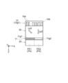
- FIG. 2A is a partial cross-sectional view (XZ cross-sectional view) illustrating an outline of an image sensor of a first example of the first embodiment.
- FIG. 2B is a partial cross-sectional view (XZ cross-sectional view) illustrating an outline of an image sensor of a first example of the first embodiment.
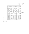
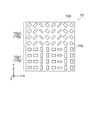
- FIG. 3 is a plan view showing an outline of the polarization control section (particularly the polarization control unit) of the first example of the first embodiment.
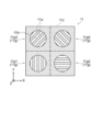
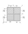
- FIG. 4 is a plan view showing an outline of an additional polarizer (particularly an additional polarizing pixel unit) of a first example of the first embodiment.
- FIG. 5 is a plan view of a polarization control section (particularly a polarization control unit) showing an example of a unit polarization control section.
- FIG. 6 is a plan view of an additional polarizer (particularly an additional polarization pixel unit) illustrating the correspondence between the additional polarization pixels of the additional polarizer shown in FIG. 4 and the vibration directions of the assigned polarization.
- FIG. 9 is a plan view showing an outline of a modified example of an additional polarizer.
- FIG. 10 is a diagram showing an example of the results (received light power distribution) of a wave simulation by the FDTD method in a photoelectric conversion section (particularly a light receiving pixel unit including the first to fourth light receiving pixels).
- FIG. 11 is a plan view showing an outline of a polarization control section (particularly, a polarization control unit) of a second example of the first embodiment.
- FIG. 12 is a plan view illustrating an outline of an additional polarizer (particularly an additional polarization pixel unit) according to a second example of the first embodiment.
- FIG. 13 is a plan view showing an outline of a polarization control section (particularly, a polarization control unit) according to a third example of the first embodiment.
- FIG. 14 is a plan view illustrating an outline of an additional polarizer (particularly an additional polarization pixel unit) according to a third example of the first embodiment.
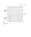
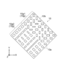
- FIG. 15 is a plan view showing an outline of a polarization control section (particularly, a polarization control unit) according to a fourth example of the first embodiment.
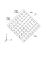
- FIG. 13 is a plan view showing an outline of a polarization control section (particularly, a polarization control unit) according to a third example of the first embodiment.
- FIG. 14 is a plan view showing an outline of a polarization control section (particularly, a polarization control unit) according to a fourth example of the first embodiment.
- FIG. 16 is a plan view illustrating an outline of an additional polarizer (particularly an additional polarization pixel unit) according to a fourth example of the first embodiment.
- FIG. 17 is a plan view showing an outline of a polarization control section (particularly, a polarization control unit) according to a fifth example of the first embodiment.
- FIG. 18 is a plan view illustrating an outline of an additional polarizer (particularly an additional polarization pixel unit) according to a fifth example of the first embodiment.
- FIG. 19 is a plan view showing an outline of a polarization control section (particularly, a polarization control unit) according to a sixth example of the first embodiment.
- FIG. 17 is a plan view showing an outline of a polarization control section (particularly, a polarization control unit) according to a fifth example of the first embodiment.
- FIG. 20 is a plan view illustrating an outline of an additional polarizer (particularly an additional polarization pixel unit) according to a sixth example of the first embodiment.
- FIG. 21 is a schematic plan view illustrating a portion of a photoelectric conversion unit including light-receiving pixels arranged in a square lattice.
- FIG. 22 is a schematic plan view illustrating a portion of a photoelectric conversion unit including light receiving pixels arranged in a diagonal lattice.
- FIG. 21 is a schematic plan view illustrating a portion of a photoelectric conversion unit including light-receiving pixels arranged in a square lattice.
- FIG. 22 is a schematic plan view illustrating a portion of a photoelectric conversion unit including light receiving pixels arranged in a diagonal lat
- FIG. 25 is a plan view of a polarization control section (particularly a polarization control unit) showing an example of a unit polarization control section of the first example of the second embodiment.
- FIG. 26 is a plan view illustrating an outline of an additional polarizer (particularly an additional polarization pixel unit) of a first example of the second embodiment.
- FIG. 27 is a perspective view illustrating an outline of an additional polarizer of a first example of the second embodiment.
- FIG. 28 is a plan view showing an outline of a polarization control section (particularly, a polarization control unit) of a second example of the second embodiment.
- FIG. 29 is a plan view illustrating an outline of an additional polarizer (particularly an additional polarization pixel unit) of a second example of the second embodiment.
- FIG. 30 is a plan view showing an outline of a polarization control section (particularly a polarization control unit) of a third example of the second embodiment.
- FIG. 31 is a plan view illustrating an outline of an additional polarizer (particularly an additional polarization pixel unit) of a third example of the second embodiment.
- FIG. 32 is a plan view showing an outline of a polarization control section (particularly a polarization control unit) of a fourth example of the second embodiment.
- FIG. 33 is a plan view illustrating an outline of an additional polarizer (particularly an additional polarization pixel unit) of a fourth example of the second embodiment.
- FIG. 34 is a plan view showing an outline of a polarization control section (particularly, a polarization control unit) of a fifth example of the second embodiment.
- FIG. 35 is a plan view illustrating an outline of an additional polarizer (particularly an additional polarization pixel unit) of a fifth example of the second embodiment.
- FIG. 36 is a plan view showing an outline of a polarization control section (particularly a polarization control unit) of a sixth example of the second embodiment.
- FIG. 37 is a plan view illustrating an outline of an additional polarizer (particularly an additional polarization pixel unit) of a sixth example of the second embodiment.
- FIG. 38 is a plan view of a polarization control section showing a first modified example of an image sensor.
- 39 is a cross-sectional view showing an example of the YZ plane of the image sensor shown in FIG.
- FIG. 40 is a cross-sectional view showing an example of the XZ plane of the image sensor shown in FIG. FIG.
- FIG. 41 is a cross-sectional view for explaining an example of a method for manufacturing an image sensor (particularly, an image sensor including a wire-grid type additional polarizer).
- FIG. 42 is a cross-sectional view illustrating an example of a manufacturing method for an image sensor (particularly, an image sensor including a wire-grid type additional polarizer).
- FIG. 43 is a cross-sectional view illustrating an example of a manufacturing method for an image sensor (particularly, an image sensor including a wire-grid type additional polarizer).
- FIG. 44 is a cross-sectional view illustrating an example of a manufacturing method for an image sensor (particularly, an image sensor including a wire-grid type additional polarizer).
- FIG. 45 is a cross-sectional view illustrating an example of a manufacturing method for an image sensor (particularly, an image sensor including a wire-grid type additional polarizer).
- FIG. 46 is a cross-sectional view illustrating an example of a manufacturing method for an image sensor (particularly, an image sensor including a wire-grid type additional polarizer).
- FIG. 47 is a cross-sectional view illustrating an example of a manufacturing method for an image sensor (particularly, an image sensor including a wire-grid type additional polarizer).
- FIG. 48 is a cross-sectional view illustrating an example of a manufacturing method for an image sensor (particularly, an image sensor including a wire-grid type additional polarizer).
- each element in the drawings is shown diagrammatically or conceptually. Therefore, the characteristics of each element in the drawings, such as the size and shape, may differ from the characteristics of the corresponding element in reality. Furthermore, the size ratios between elements in the drawings may differ from the size ratios between corresponding elements in the actual device. Furthermore, the size and shape of each element and the size ratios between elements do not necessarily match between drawings, and one or more specific elements may be exaggerated in each drawing.
- the X, Y, and Z directions are mutually perpendicular.
- the X direction may correspond to the horizontal direction
- the Y direction may correspond to the vertical direction (height direction)
- the Z direction may correspond to the depth direction.
- FIG. 1 is a schematic diagram showing an example of the configuration of an image sensor 1.
- the polarization control unit (polarization splitter) 10, additional polarizer 11, and photoelectric conversion unit 20 are shown as viewed from an angle, and the optical system OP is shown as viewed from the side.
- Image sensor 1 can typically be configured as a CCD (Charge Coupled Device) image sensor or a CMOS (Complementary Metal Oxide Semiconductor) image sensor. However, image sensor 1 can be configured as any imaging device.
- CCD Charge Coupled Device
- CMOS Complementary Metal Oxide Semiconductor
- the image sensor 1 receives light from an external subject, acquires data on various pieces of information including the intensity and color of the light, and generates an image of the subject.
- the polarization information of the light from the subject contains useful information that cannot be acquired from the light intensity and color (wavelength) alone, and may include, for example, information on the shape of the subject's surface and information on the material of the subject. Polarized imaging technology that uses such polarization information can be used in a variety of fields, such as in-vehicle cameras, IoT (Internet of Things) devices, and medical devices.
- the image sensor 1 shown in FIG. 1 includes an optical system OP, a polarization control unit 10, an additional polarizer 11, and a photoelectric conversion unit 20.
- the optical system OP includes a lens that collects incident light L from a subject.
- the incident light L that passes through the optical system OP includes frontal incident light La that travels in the optical axis direction of the principal ray, and oblique incident light Lb that travels in a direction oblique to the optical axis of the principal ray.
- the optical axis direction coincides with the Z direction.
- the photoelectric conversion unit 20 includes a number of light-receiving pixels PX that receive incident light L (particularly a number of polarized lights extracted from the incident light L).
- the multiple light-receiving pixels PX are arranged two-dimensionally in the X and Y directions, and the photoelectric conversion unit 20 as a whole has a rectangular shape with sides extending in the X and Y directions.
- the light-receiving pixel PX located at the center of the photoelectric conversion unit 20 (0% image height) receives frontal incident light La.
- the light-receiving pixel PX located away from the center of the photoelectric conversion unit 20 receives oblique incident light Lb.
- Each light-receiving pixel PX has a photodiode made of a Si (silicon) semiconductor material or the like. Note that the light absorption coefficient of each light-receiving pixel PX is not necessarily large, since the absorption rate (sensitivity) of the incident light can change depending on the wavelength (e.g., 940 nm) of the incident light (polarized light). Therefore, as an example, a light scatterer (not shown) may be placed on the surface (light-receiving surface) of each light-receiving pixel PX to scatter the incident light, thereby increasing the optical path length of the incident light at each light-receiving pixel PX and improving the sensitivity of each light-receiving pixel PX.
- a light scatterer may be placed on the surface (light-receiving surface) of each light-receiving pixel PX to scatter the incident light, thereby increasing the optical path length of the incident light at each light-receiving pixel PX and improving the sensitivity
- the polarization control unit 10 and the additional polarizer 11 are disposed in the optical path between the optical system OP and the photoelectric conversion unit 20, and are arranged to cover the multiple light receiving pixels PX (particularly the light receiving surfaces) of the photoelectric conversion unit 20.
- the polarization control unit 10 has a metasurface structure including a large number (multiple) of microstructures also called "meta-atoms".
- the additional polarizer 11 is a polarizer that does not have a metasurface structure.
- the additional polarizer 11 it is possible to use a polarizer of any structure (for example, a wire grid type polarizer or a photonic crystal type polarizer described below) that can extract the desired linearly polarized light from the incident light L.
- the polarization control unit 10 and the additional polarizer 11 in the portions covering the light-receiving pixels PX located in the center of the photoelectric conversion unit 20 perform polarization control of the frontal incident light La, and focus the frontal incident light La (particularly the polarized component) on the light-receiving pixels PX located in the center of the photoelectric conversion unit 20.
- the polarization control unit 10 and the additional polarizer 11 in the portions covering the light-receiving pixels PX located at the ends of the photoelectric conversion unit 20 perform polarization control of the oblique incident light Lb, and focus the oblique incident light Lb (particularly the polarized component) on the light-receiving pixels PX located at the ends of the photoelectric conversion unit 20. In this way, each portion of the polarization control unit 10 and the additional polarizer 11 selectively passes specific polarized components contained in the incident light L incident at various angles, and focuses them on the corresponding light-receiving pixels PX.
- the additional polarizer 11 is disposed between the polarization control unit 10 and the photoelectric conversion unit 20 in the optical axis direction, and receives multiple polarized light from the polarization control unit 10 and selectively transmits the multiple polarized light.
- the polarization control unit 10 focuses the multiple polarized light toward different regions of the additional polarizer 11 (multiple additional polarization pixels described below), as described below.
- the multiple light-receiving pixels PX of the photoelectric conversion unit 20 receive the multiple polarized light selectively emitted from the additional polarizer 11.
- a polarization control unit 10 (particularly a unit polarization control unit described below) and an additional polarizer 11 (particularly an additional polarization pixel described below) are assigned to each light-receiving pixel PX so that polarized light vibrating in the desired direction is selectively incident thereon.
- the multiple polarized lights that are transmitted through the polarization control unit 10 and the additional polarizer 11 and received by the photoelectric conversion unit 20 include a first polarized light, a second polarized light, a third polarized light, and a fourth polarized light that have different vibration directions.
- the specific vibration directions of the first to fourth polarized light are not limited.
- the first and second polarized light have vibration directions that differ by 90 degrees from each other
- the third and fourth polarized light have vibration directions that differ by 90 degrees from each other
- the second and third polarized light have vibration directions that differ by 45 degrees from each other.
- the first to fourth polarized light have vibration directions of 0 degrees, +90 degrees, -45 degrees, and +45 degrees based on the propagation direction, respectively.
- the vibration direction of 0 degrees may be a direction that coincides with the X direction
- the vibration direction of +90 degrees may be a direction that coincides with the Y direction
- the vibration directions of -45 degrees and +45 degrees may be directions that are oblique to the X direction and the Y direction.
- the image sensor 1 (particularly the polarization control unit 10 and the additional polarizer 11) described above can have various configurations. A typical embodiment of the image sensor 1 will be described below.
- the additional polarizer 11 in this embodiment includes a wire grid type polarizer.
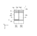
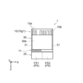
- FIG. 2A and 2B are partial cross-sectional views (XZ cross-sectional views) showing an outline of the image sensor 1 of the first example of the first embodiment, and show the case where the incident light L is perpendicularly incident on the image sensor 1 (particularly the polarization control unit 10).
- FIG. 2A shows the first light receiving pixel PX1 and the second light receiving pixel PX2
- FIG. 2B shows the third light receiving pixel PX3 and the fourth light receiving pixel PX4.
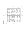
- FIG. 3 is a plan view showing an outline of the polarization control unit 10 (particularly the polarization control unit) of the first example of the first embodiment.
- FIG. 4 is a plan view showing an outline of the additional polarizer 11 (particularly the additional polarization pixel unit) of the first example of the first embodiment.
- FIG. 5 is a plan view of the polarization control unit 10 (particularly the polarization control unit) showing an example of a unit polarization control unit 10g.
- FIG. 6 is a plan view of the additional polarizer 11 (particularly the additional polarization pixel unit) showing the correspondence between the additional polarization pixels 11g of the additional polarizer 11 shown in FIG. 4 and the vibration directions P1 to P4 of the assigned polarization.
- the polarization control unit 10, the additional polarizer 11, and the photoelectric conversion unit 20 each have a square pixel array.
- four light receiving pixels PX arranged in a square lattice arrangement with two light receiving pixels PX lined up in the X direction and two light receiving pixels PX lined up in the Y direction, form one light receiving pixel unit, and multiple such light receiving pixel units are arranged in the X direction and Y direction.
- the four light receiving pixels PX (first light receiving pixel PX1 to fourth light receiving pixel PX4) included in each light receiving pixel unit are assigned to the first polarization Lp1 to fourth polarization Lp4, respectively (see Figures 2A and 2B).
- the phase of the polarization information acquired by the image sensor 1, which is capable of separating and receiving polarized light vibrating in four directions, makes it possible to estimate the normal vector of the subject's surface, and thus to grasp the shape of the subject.
- the additional polarizer 11 which is a wire grid polarizer, includes a large number of wires 11a (see FIG. 4).
- Each wire 11a is made of a metal such as aluminum (Al), but may be made of other materials.
- the inter-wire portions 11b between adjacent wires 11a are polarized light transmitting regions, and may be configured as spaces (air regions) or may be configured of a low refractive index material (for example, silicon dioxide (SiO 2 )).
- a low refractive index material for example, silicon dioxide (SiO 2 )
- the additional polarizer 11 is divided into a number of additional polarization pixels 11g as shown in FIG. 4.
- the multiple additional polarization pixels 11g included in the additional polarizer 11 in this example have a square lattice arrangement.
- four additional polarization pixels 11g arranged in a square lattice arrangement with two additional polarization pixels 11g arranged in the X direction and two additional polarization pixels 11g arranged in the Y direction, constitute one additional polarization pixel unit, and multiple such additional polarization pixel units are arranged in the X direction and Y direction.
- These four additional polarization pixels 11g included in each additional polarization pixel unit are assigned to the first polarization Lp1 to the fourth polarization Lp4, respectively.
- each additional polarization pixel 11g selectively transmits one of the first polarization Lp1, the second polarization Lp2, the third polarization Lp3, and the fourth polarization Lp4.
- the extension direction of the wire line 11a of each additional polarization pixel 11g is determined according to the vibration direction of the assigned polarization, and is a direction that forms an angle of 90 degrees with respect to the vibration direction of the assigned polarization (see FIG. 6).
- the additional polarizer 11 further has a frame-shaped additional polarizing light-shielding portion 11c (see FIG. 4) that is arranged to surround each additional polarizing pixel 11g.
- the additional polarizing light-shielding portion 11c has any configuration and any composition that can block the transmission of light (particularly polarized light). Therefore, the additional polarizing light-shielding portion 11c may be configured to block light by reflecting light, or may be configured to block light by absorbing light.
- the additional polarized light shielding portion 11c thus provided between adjacent additional polarized pixels 11g can suppress leakage (crosstalk) of light (especially polarized light) between adjacent additional polarized pixels 11g, which is advantageous for obtaining a high extinction ratio.
- the polarization control unit 10 of the metasurface structure is provided upstream of the additional polarizer 11 in the incident direction A0 of the incident light L.
- This polarization control unit 10 exhibits a polarization splitter function that selectively transmits and separates multiple polarized lights (first polarized light Lp1 to fourth polarized light Lp4) in the incident light L.
- a waveguide 30 is provided between the polarization control unit 10 and the photoelectric conversion unit 20 (each light receiving pixel PX).
- the waveguide 30 can have any configuration, and the material that can be used to form the waveguide 30 is not limited.
- the waveguide 30 may be made of any transparent material selected from the group consisting of amorphous silicon, polycrystalline silicon, germanium, titanium oxide, niobium oxide, tantalum oxide, aluminum oxide, hafnium oxide, silicon nitride, silicon oxide, silicon nitride oxide, silicon carbide, silicon oxide carbide, silicon nitride carbide, and zirconium oxide.
- the multiple meta-atoms (microstructures) 10a included in the polarization control unit 10 are arranged two-dimensionally in the X and Y directions as shown in FIG. 3, and are arranged in a plane that is approximately parallel to the light receiving surface of the light receiving pixel PX (photoelectric conversion unit 20).
- the refractive index of each meta-atom 10a is greater than the refractive index of the area between the meta-atoms 10a (i.e., the peripheral portion 10b of the structure).
- each meta-atom 10a may have any configuration, and the material that can form each meta-atom 10a is not limited.
- each meta-atom 10a may be made of any of amorphous silicon ( ⁇ -Si), polycrystalline silicon (Poly-Si), germanium, titanium oxide (TiO 2 ), niobium oxide, tantalum oxide, aluminum oxide, hafnium oxide, silicon nitride (SiN, Si 3 N 4 ), silicon oxide, silicon nitride oxide, silicon carbide, silicon oxide carbide, silicon nitride carbide, zirconium oxide, gallium nitride (GaN), gallium arsenide (GaAs), and indium phosphide (InP).
- ⁇ -Si amorphous silicon
- Poly-Si polycrystalline silicon
- germanium titanium oxide
- TiO 2 titanium oxide
- niobium oxide tantalum oxide
- aluminum oxide hafnium oxide
- silicon nitride SiN, Si 3 N 4
- the regions between the meta-atoms 10a can have any configuration, for example they can be provided as spaces or can be made of a solid material such as silicon dioxide.
- the meta-atom 10a and the waveguide 30 are made of different materials.
- the waveguide 30 is made of silicon oxide film or titanium oxide
- the meta-atom 10a may be made of single crystal silicon or amorphous silicon.
- the peripheral portion 10b of the structure may be made of a material different from that of the waveguide 30, or may be made of the same material as the waveguide 30.
- Each meta atom 10a has a pillar shape, and is ideally configured as a rectangular parallelepiped with a rectangular cross-sectional shape and planar shape. In reality, however, when the polarization control unit 10 is fabricated by processing using a lithography photomask, the corners of each meta atom 10a may be rounded. Even if the corners of each meta atom 10a are rounded, the polarization control unit 10 can fully function as a polarization splitter. In this way, the shape of each meta atom 10a is not limited, and the cross-sectional shape and planar shape of each meta atom 10a may be any polygonal, elliptical, hollow, or other shape.
- the polarization control unit 10 includes multiple types of unit polarization control units 10g that separate and emit (focus) polarized light that vibrates in different directions (see Figure 5).
- Each unit polarization control unit 10g in this example is provided in a range corresponding to two light-receiving pixels PX (i.e., an area covering two light-receiving pixels PX), and selectively emits two polarized components in the incident light L in directions different from each other to focus the light. This enables each unit polarization control unit 10g to focus polarized light that is incident on a range corresponding to two pixels (multiple pixels) of the incident light L onto the additional polarizer 11 (additional polarization pixel 11g) and photoelectric conversion unit 20 (light-receiving pixel PX) that correspond to one pixel (single pixel).
- the multiple unit polarization control units 10g include a first unit polarization control unit 10g1 and a second unit polarization control unit 10g2.
- one first unit polarization control unit 10g1 and one second unit polarization control unit 10g2 adjacent in the Y direction are considered as one polarization control unit, and multiple such polarization control units are arranged in the X and Y directions.
- the first unit polarization control unit 10g1 is assigned to the first additional polarization pixel 11g1 and the second additional polarization pixel 11g2, and is therefore assigned to the first light receiving pixel PX1 and the second light receiving pixel PX2.
- the second unit polarization control unit 10g2 is assigned to the third additional polarization pixel 11g3 and the fourth additional polarization pixel 11g4, and is therefore assigned to the third light receiving pixel PX3 and the fourth light receiving pixel PX4.
- the multiple meta atoms 10a included in each first unit polarization control unit 10g1 are linearly arranged along each of the vibration direction P1 (0 degrees: X direction) of the first polarized light Lp1 and the vibration direction P2 (90 degrees: Y direction) of the second polarized light Lp2 in the incident light L.
- the multiple meta atoms 10a of each first unit polarization control unit 10g1 include multiple meta atoms 10a whose sizes are different from each other in the vibration direction P1 (X direction) of the first polarized light Lp1 and the vibration direction P2 (Y direction) of the second polarized light Lp2 in the incident light L.
- each second unit polarization control unit 10g2 are linearly arranged along the vibration direction P3 (-45 degrees) of the third polarization Lp3 and the vibration direction P4 (+45 degrees) of the fourth polarization Lp4, and include multiple meta atoms 10a whose sizes in the vibration directions P3 and P4 are different from each other.
- each unit polarization control unit 10g selectively emits (focuses) the polarized components in the incident light L toward the additional polarizer 11 (particularly the corresponding additional polarization pixel 11g).
- the first unit polarization control unit 10g1 selectively transmits the first polarized light Lp1 and the second polarized light Lp2 in the incident light L, and outputs (concentrates) the first polarized light Lp1 toward the first additional polarization pixel 11g1 while outputting (concentrates) the second polarized light Lp2 toward the second additional polarization pixel 11g2.
- the traveling direction of the first polarized light Lp1 from the first unit polarization control unit 10g1 toward the first additional polarization pixel 11g1 is represented by "A1”.
- the traveling direction of the second polarized light Lp2 from the first unit polarization control unit 10g1 toward the second additional polarization pixel 11g2 is represented by "A2".
- the first polarized light Lp1 emitted from the portion of the first unit polarization control unit 10g1 that covers the first light receiving pixel PX1 travels toward the first light receiving pixel PX1 along the Z direction or along an oblique direction that is slightly inclined relative to the Z direction.
- the first polarized light Lp1 emitted from the portion of the first unit polarization control unit 10g1 that covers the second light receiving pixel PX2 travels toward the first light receiving pixel PX1 along an oblique direction that is greatly inclined relative to the Z direction (the lower left direction in FIG. 7).
- the second polarized light Lp2 emitted from the portion of the first unit polarization control unit 10g1 that covers the second light receiving pixel PX2 travels toward the second light receiving pixel PX2 along the Z direction or along an oblique direction that is slightly inclined relative to the Z direction.
- the second polarized light Lp2 emitted from the portion of the first unit polarization control unit 10g1 that covers the first light receiving pixel PX1 travels toward the second light receiving pixel PX2 along an oblique direction that is greatly inclined relative to the Z direction (the lower right direction in FIG. 8).
- the second unit polarization control unit 10g2 selectively transmits the third polarized light Lp3 and the fourth polarized light Lp4, and outputs (focuses) the third polarized light Lp3 toward the third additional polarization pixel 11g3 while outputting (focuses) the fourth polarized light Lp4 toward the fourth additional polarization pixel 11g4.
- the traveling direction of the third polarized light Lp3 from the second unit polarization control unit 10g2 toward the third additional polarization pixel 11g3 is represented by "A3”.
- the traveling direction of the fourth polarized light Lp4 from the second unit polarization control unit 10g2 toward the fourth additional polarization pixel 11g4 is represented by "A4".
- the polarization control unit 10 can focus the corresponding desired polarized light on each additional polarization pixel 11g of the additional polarizer 11. As a result, it is possible to suppress the incidence of undesired polarized light on each additional polarization pixel 11g, and effectively reduce the loss of light in the additional polarizer 11.
- Each additional polarization pixel 11g also effectively blocks the transmission of undesired polarization while allowing the transmission of the desired polarization.
- the image sensor 1 of this example therefore ensures good light-receiving sensitivity to the desired polarized light in each light-receiving pixel PX while suppressing reception of undesired polarized light, which is advantageous in achieving a high extinction ratio.
- the image sensor 1 may have a configuration different from that shown in Figures 2A to 8 above.
- FIG. 9 is a plan view showing an outline of one modified example of the additional polarizer 11.
- the additional polarized light-shielding portion 11c of the additional polarizer 11 is provided so that the distance between the substantial light-transmitting areas (inter-wire portions 11b) of adjacent additional polarized pixels 11g is large.
- the additional polarized light-shielding portion 11c is provided so that the substantial light-transmitting area (inter-wire portions 11b) of each additional polarized pixel 11g has a circular planar shape at the center of each pixel.
- the additional polarized light shielding portion 11c is provided as an aperture that limits the light-transmitting area in each additional polarized pixel 11g through which light (particularly polarized light) can pass, thereby suppressing the incidence of undesired polarized light on each light-receiving pixel PX, thereby improving the extinction ratio.
- incident light L having a wavelength of 940 nm was made to be perpendicularly incident on the image sensor 1 having the structure shown in Figures 1 to 8.
- FIG. 10 is a diagram showing an example of the results (receiving light power distribution) of a wave simulation performed by the FDTD method in the photoelectric conversion unit 20 (particularly the light receiving pixel unit PXg including the first light receiving pixel PX1 to the fourth light receiving pixel PX4).
- areas represented in colors closer to white indicate that they receive the first polarized light Lp1 more strongly, and areas represented in colors closer to black indicate that the received light intensity of the first polarized light Lp1 is weaker.
- the first light receiving pixel PX1 received the first polarized light Lp1 relatively strongly, and the light receiving intensity of the first light receiving pixel PX1 by the other light receiving pixels PX (particularly the second light receiving pixel PX2) was relatively weak.
- the first polarized light Lp1 is focused on the first additional polarization pixel 11g1 by the polarization control unit 10 (particularly the first unit polarization control unit 10g1), and is guided to pass through the first additional polarization pixel 11g1 and to be incident on the first light receiving pixel PX1 in a concentrated manner.
- the first polarized light Lp1 is guided by the polarization control unit 10 so that it does not enter any additional polarization pixels 11g other than the first additional polarization pixel 11g1, and thus does not actually enter any light receiving pixel PX other than the first light receiving pixel PX1.
- the simulation results shown in FIG. 10 are consistent with the structural characteristics of the image sensor 1 shown in FIGS. 1 to 8, and confirm that the image sensor 1 shown in FIGS. 1 to 8 is advantageous for selectively concentrating and receiving the first polarized light Lp1 by the first light receiving pixel PX1.
- Figure 10 shows the simulation results for the first polarized light Lp1
- similar simulation results were obtained for the other polarized lights (second polarized light Lp2 to fourth polarized light Lp4).
- the simulation results support the idea that the image sensor 1 shown in Figures 1 to 8 is advantageous for selectively concentrating and receiving the second polarized light Lp2 to fourth polarized light Lp4 by the second light receiving pixel PX2 to fourth light receiving pixel PX4, respectively.
- simulations based on the presence or absence of the polarization control unit 10 and the additional polarizer 11. That is, simulations were also performed based on "an image sensor 1 having a polarization control unit 10 and an additional polarizer 11" and “an image sensor 1 having only one of the polarization control unit 10 and the additional polarizer 11 (without the other)."
- the "image sensor 1 having the polarization control unit 10 and the additional polarizer 11” has the structure shown in the above-mentioned Figures 1 to 8.
- the “image sensor 1 having only one of the polarization control unit 10 and the additional polarizer 11” has a structure in which the polarization control unit 10 or the additional polarizer 11 has been removed from the structure shown in the above-mentioned Figures 1 to 8.
- the configuration other than the polarization control unit 10 and the additional polarizer 11 was common among the image sensors 1 for which the simulations were performed.
- Table 1 shows example results of a simulation performed based on "an image sensor 1 having a polarization control unit 10 and an additional polarizer 11" and "an image sensor 1 having only one of the polarization control unit 10 and the additional polarizer 11.”
- incident light L (particularly the first polarized light Lp1 (i.e., the incident light L that does not include the second polarized light Lp2 to the fourth polarized light Lp4 and only includes the first polarized light Lp1)) with the same light intensity was made to enter the image sensor 1 perpendicularly.
- light receiving power of the first light receiving pixel and “light receiving power of the second light receiving pixel” are numerical values indicating the light receiving intensity of the first polarized light Lp1 by the first light receiving pixel PX1 and the second light receiving pixel PX2, respectively.
- the light receiving power of the first light receiving pixel PX1 for the first polarization Lp1 increases by about three times compared to when only the additional polarizer 11 is provided (number “2").
- the light receiving power of the second light receiving pixel PX2 for the first polarization Lp1 decreases to about 1/5 compared to when only the additional polarizer 11 is provided (number "2").
- the extinction ratio increased by about 12 times when the polarization control unit 10 and the additional polarizer 11 were provided (number “3") compared to when only the additional polarizer 11 was provided (number “2"). Also, the extinction ratio increased by about 204 times when the polarization control unit 10 and the additional polarizer 11 were provided (number "3") compared to when only the polarization control unit 10 was provided (number "1").
- FIG. 11 is a plan view showing an outline of the polarization control section 10 (particularly the polarization control unit) of the second example of the first embodiment.
- FIG. 12 is a plan view showing an outline of the additional polarizer 11 (particularly the additional polarization pixel unit) of the second example of the first embodiment.
- the arrangement of the third light receiving pixel PX3 and the fourth light receiving pixel PX4 in each light receiving pixel unit PXg of the photoelectric conversion unit 20 is swapped with the arrangement in the first example described above (see FIG. 10). That is, the fourth light receiving pixel PX4 is arranged adjacent to the first light receiving pixel PX1 in the Y direction, and the third light receiving pixel PX3 is arranged adjacent to the second light receiving pixel PX2 in the Y direction.
- the arrangement of the third additional polarization pixel 11g3 and the fourth additional polarization pixel 11g4 in each additional polarization pixel unit of the additional polarizer 11 is swapped with the arrangement in the first example (see FIG. 4). That is, the fourth additional polarization pixel 11g4 is arranged adjacent to the first additional polarization pixel 11g1 in the Y direction, and the third additional polarization pixel 11g3 is arranged adjacent to the second additional polarization pixel 11g2 in the Y direction.
- the arrangement of the first light receiving pixel PX1 and the second light receiving pixel PX2 of each light receiving pixel unit PXg in the second example is the same as the arrangement in the first example described above (see FIG. 10). Therefore, in the second example, as shown in FIG. 12, the arrangement of the first additional polarization pixel 11g1 and the second additional polarization pixel 11g2 in each additional polarization pixel unit of the additional polarizer 11 is the same as the arrangement in the first example (see FIG. 4).
- the polarization control unit 10 has a metasurface structure (multiple metaatoms 10a and a structure peripheral portion 10b) that selectively emits the first polarized light Lp1 to the fourth polarized light Lp4 toward each of the above-mentioned first additional polarization pixel 11g1 to fourth additional polarization pixel 11g4.
- the first polarized light Lp1 to the fourth polarized light Lp4 are focused on the first additional polarization pixel 11g1 to the fourth additional polarization pixel 11g4 of the additional polarizer 11 by the polarization control unit 10, and selectively transmitted through each of the first additional polarization pixel 11g1 to the fourth additional polarization pixel 11g4.
- the first polarized light Lp1 to the fourth polarized light Lp4 are selectively received by each of the first light receiving pixel PX1 to the fourth light receiving pixel PX4 of the photoelectric conversion unit 20.
- FIG. 13 is a plan view showing an outline of the polarization control section 10 (particularly the polarization control unit) of the third example of the first embodiment.
- FIG. 14 is a plan view showing an outline of the additional polarizer 11 (particularly the additional polarization pixel unit) of the third example of the first embodiment.
- the arrangement of the first light receiving pixel PX1 and the second light receiving pixel PX2 in each light receiving pixel unit PXg of the photoelectric conversion unit 20 is swapped with the arrangement in the first example described above (see FIG. 10). That is, the fourth light receiving pixel PX4 is arranged adjacent to the first light receiving pixel PX1 in the Y direction, and the third light receiving pixel PX3 is arranged adjacent to the second light receiving pixel PX2 in the Y direction.
- the arrangement of the first additional polarization pixel 11g1 and the second additional polarization pixel 11g2 in each additional polarization pixel unit of the additional polarizer 11 is swapped with the arrangement in the first example (see FIG. 4). That is, the fourth additional polarization pixel 11g4 is arranged adjacent to the first additional polarization pixel 11g1 in the Y direction, and the third additional polarization pixel 11g3 is arranged adjacent to the second additional polarization pixel 11g2 in the Y direction.
- the arrangement of the third light receiving pixel PX3 and the fourth light receiving pixel PX4 of each light receiving pixel unit PXg in the third example is the same as the arrangement in the first example described above. Also, the arrangement of the third additional polarization pixel 11g3 and the fourth additional polarization pixel 11g4 of each additional polarization pixel unit in the third example is the same as the arrangement in the first example described above.
- the polarization control unit 10 has a metasurface structure (multiple metaatoms 10a and a structure peripheral portion 10b) that selectively emits the first polarized light Lp1 to the fourth polarized light Lp4 toward each of the above-mentioned first additional polarization pixel 11g1 to fourth additional polarization pixel 11g4.
- the first polarized light Lp1 to the fourth polarized light Lp4 are focused on the first additional polarization pixel 11g1 to the fourth additional polarization pixel 11g4 of the additional polarizer 11 by the polarization control unit 10, and selectively transmitted through each of the first additional polarization pixel 11g1 to the fourth additional polarization pixel 11g4.
- the first polarized light Lp1 to the fourth polarized light Lp4 are selectively received by each of the first light receiving pixel PX1 to the fourth light receiving pixel PX4 of the photoelectric conversion unit 20.
- FIG. 15 is a plan view showing an outline of the polarization control unit 10 (particularly the polarization control unit) of the fourth example of the first embodiment.
- FIG. 16 is a plan view showing an outline of the additional polarizer 11 (particularly the additional polarization pixel unit) of the fourth example of the first embodiment.
- FIG. 17 is a plan view showing an outline of the polarization control unit 10 (particularly the polarization control unit) of the fifth example of the first embodiment.
- FIG. 18 is a plan view showing an outline of the additional polarizer 11 (particularly the additional polarization pixel unit) of the fifth example of the first embodiment.
- FIG. 19 is a plan view showing an outline of the polarization control unit 10 (particularly the polarization control unit) of the sixth example of the first embodiment.
- FIG. 20 is a plan view showing an outline of the additional polarizer 11 (particularly the additional polarization pixel unit) of the sixth example of the first embodiment.
- the multiple light receiving pixels PX have a diagonal lattice arrangement and are arranged two-dimensionally in a direction tilted with respect to each of the X and Y directions (for example, a direction tilted at 45 degrees with respect to each of the X and Y directions).
- the multiple unit polarization control units 10g included in the polarization control unit 10 have a diagonal lattice arrangement (see Figures 15, 17, and 19).
- the multiple additional polarization pixels 11g included in the additional polarizer 11 have a diagonal lattice arrangement (see Figures 16, 18, and 20).
- a plurality of light receiving pixel units, a plurality of additional polarization pixel units, and a plurality of polarization control units are arranged two-dimensionally in directions oblique to each of the X and Y directions.
- the relative arrangements of the first to fourth light receiving pixels PX1 to PX4 that receive the first to fourth polarized lights Lp1 to Lp4, respectively, are different.
- the first light receiving pixel PX1 and the third light receiving pixel PX3 are arranged in the X direction
- the second light receiving pixel PX2 and the fourth light receiving pixel PX4 are arranged in the Y direction. Therefore, as shown in FIG. 16, in each additional polarization unit, the first additional polarization pixel 11g1 and the third additional polarization pixel 11g3 are arranged in the X direction, and the second additional polarization pixel 11g2 and the fourth additional polarization pixel 11g4 are arranged in the Y direction.
- the third light receiving pixel PX3 and the second light receiving pixel PX2 are arranged in the X direction, and the fourth light receiving pixel PX4 and the first light receiving pixel PX1 are arranged in the Y direction. Therefore, as shown in FIG. 18, in each additional polarization unit, the third additional polarization pixel 11g3 and the second additional polarization pixel 11g2 are arranged in the X direction, and the fourth additional polarization pixel 11g4 and the first additional polarization pixel 11g1 are arranged in the Y direction.
- the fourth light receiving pixel PX4 and the first light receiving pixel PX1 are arranged in the X direction, and the third light receiving pixel PX3 and the second light receiving pixel PX2 are arranged in the Y direction. Therefore, as shown in FIG. 20, in each additional polarization unit, the fourth additional polarization pixel 11g4 and the first additional polarization pixel 11g1 are arranged in the X direction, and the third additional polarization pixel 11g3 and the second additional polarization pixel 11g2 are arranged in the Y direction.
- FIG. 21 is a schematic plan view showing a portion of a photoelectric conversion unit 20 including light-receiving pixels PX arranged in a square lattice.
- FIG. 22 is a schematic plan view showing a portion of a photoelectric conversion unit 20 including light-receiving pixels PX arranged in a diagonal lattice.
- a specific light receiving pixel (one of the first light receiving pixel PX1 to the fourth light receiving pixel PX4) for receiving a specific polarized light (one of the first polarized light Lp1 to the fourth polarized light Lp4) is represented by "PXn.”
- the periodic distance in the X direction between the specific light receiving pixels PXn (X-direction periodic distance) is represented by "Tx”
- the periodic distance in the Y direction between the specific light receiving pixels PXn (Y-direction periodic distance) is represented by "Ty.”
- the light-receiving pixels PX in the diagonal lattice arrangement have smaller periodic distances Tx and Ty in the X direction (specifically, 1/ ⁇ 2 times the periodic distances Tx and Ty in the Y direction) than the light-receiving pixels PX in the square lattice arrangement (FIG. 21).
- the light-receiving pixels PX in the diagonal lattice array (FIG. 22) have substantially finer (higher) resolution in the X direction (corresponding to the horizontal direction) and Y direction (corresponding to the vertical direction) compared to the light-receiving pixels PX in the square lattice array (FIG. 21). Therefore, the image sensors 1 in the fourth to sixth examples described above, which are based on a diagonal lattice array, are advantageous in obtaining images with higher resolution in the horizontal and vertical directions compared to the image sensors 1 in the first to third examples described above, which are based on a square lattice array.
- the image sensor 1 of the fourth to sixth examples described above which is based on a diagonal grid array, is advantageous for acquiring images with a resolution that is preferable in terms of human visual characteristics.
- the metasurface-structured polarization control unit 10 collects light from a wide range and emits multiple polarized lights (four types of polarized light) toward separate additional polarization pixels 11g and separate light-receiving pixels PX.
- an image sensor 1 equipped with such a polarization control unit 10 and additional polarizer 11 is prone to degradation of resolution, but by adopting the above-mentioned diagonal lattice array, degradation of resolution can be effectively suppressed.
- the image sensors 1 of the fourth to sixth examples based on the diagonal lattice array may have the same configuration as the image sensors 1 of the first to third examples based on the square lattice array, except for the configuration described above.
- the additional polarizers 11 of the second to sixth examples may have additional polarized light-shielding portions 11c that limit the effective light-transmitting area of each additional polarized pixel 11g and increase the distance between the light-transmitting areas of adjacent additional polarized pixels 11g, as shown in FIG. 9, as in the first example.
- the additional polarizer 11 in this embodiment includes a photonic crystal polarizer.
- FIG. 25 is a plan view of the polarization control unit 10 (particularly the polarization control unit) showing an example of the unit polarization control unit 10g of the first example of the second embodiment.
- FIG. 26 is a plan view showing an outline of the additional polarizer 11 (particularly the additional polarization pixel unit) of the first example of the second embodiment.
- FIG. 27 is a perspective view showing an outline of the additional polarizer 11 of the first example of the second embodiment.
- the photonic crystal polarizer that constitutes the additional polarizer 11 has the property of selectively transmitting and emitting polarized light depending on the vibration direction, similar to the wire grid polarizer described above.
- a photonic crystal polarizer has a photonic crystal structure in which materials with different refractive indices are arranged periodically, and the additional polarizer 11 in this example includes a low refractive index material 11d and a high refractive index material 11e arranged periodically.
- the additional polarizer 11 can form a one-dimensional photonic band gap by having a multilayer film of, for example, an amorphous silicon ( ⁇ -Si) layer with a high refractive index and a silicon oxide (SiO 2 ) layer with a low refractive index.
- the photonic crystal type additional polarizer 11 may be composed of a combination of a low refractive index material 11d and a high refractive index material 11e based on other compositions.
- the high refractive index material 11e may be titanium oxide ( TiO2 ), silicon nitride ( Si3N4 ), tantalum oxide ( Ta2O5 ) or hafnium oxide ( HfO2 ).
- the additional polarizing unit of the additional polarizer 11 in this example includes a first additional polarizing pixel 11g1 to a fourth additional polarizing pixel 11g4 in a square pixel array having a photonic crystal structure that selectively transmits each of the first polarized light Lp1 to the fourth polarized light Lp4.
- a frame-shaped member with excellent light-shielding properties e.g., a light-shielding film made of tungsten (W) is installed as the additional polarized light-shielding portion 11c provided between adjacent additional polarizing pixels 11g.
- the first polarized light Lp1 to the fourth polarized light Lp4 are focused on the first additional polarization pixel 11g1 to the fourth additional polarization pixel 11g4 of the additional polarizer 11 by the polarization control unit 10.
- the first polarized light Lp1 to the fourth polarized light Lp4 are selectively transmitted through the first additional polarization pixel 11g1 to the fourth additional polarization pixel 11g4, respectively, and are selectively received by the first light receiving pixel PX1 to the fourth light receiving pixel PX4 of the photoelectric conversion unit 20, respectively.
- FIG. 28 is a plan view showing an outline of the polarization control unit 10 (particularly the polarization control unit) of the second example of the second embodiment.
- FIG. 29 is a plan view showing an outline of the additional polarizer 11 (particularly the additional polarization pixel unit) of the second example of the second embodiment.
- FIG. 30 is a plan view showing an outline of the polarization control unit 10 (particularly the polarization control unit) of the third example of the second embodiment.
- FIG. 31 is a plan view showing an outline of the additional polarizer 11 (particularly the additional polarization pixel unit) of the third example of the second embodiment.
- FIG. 32 is a plan view showing an outline of the polarization control unit 10 (particularly the polarization control unit) of the fourth example of the second embodiment.
- FIG. 33 is a plan view showing an outline of the additional polarizer 11 (particularly the additional polarization pixel unit) of the fourth example of the second embodiment.
- FIG. 34 is a plan view showing an outline of the polarization control unit 10 (particularly the polarization control unit) of the fifth example of the second embodiment.
- FIG. 35 is a plan view showing an outline of the additional polarizer 11 (particularly the additional polarization pixel unit) of the fifth example of the second embodiment.
- FIG. 36 is a plan view showing an outline of the polarization control unit 10 (particularly the polarization control unit) of the sixth example of the second embodiment.
- FIG. 37 is a plan view showing an outline of the additional polarizer 11 (particularly the additional polarization pixel unit) of the sixth example of the second embodiment.
- the first to sixth examples of the second embodiment are different from each other in the relative arrangement between the first light receiving pixel PX1 to the fourth light receiving pixel PX4 that receive the first polarized light Lp1 to the fourth polarized light Lp4, as in the first to sixth examples of the first embodiment described above.
- first light receiving pixel PX1 to the fourth light receiving pixel PX4 in the first to sixth examples of the second embodiment are arranged in the same manner as the first light receiving pixel PX1 to the fourth light receiving pixel PX4 in the first to sixth examples of the first embodiment described above.
- the first unit polarization control unit 10g1 and the second unit polarization control unit 10g2 in the first to sixth examples of the second embodiment are arranged in the same manner as the first to sixth examples of the first embodiment (see Figures 25, 28, 30, 32, 34, and 36).
- the first to fourth additional polarization pixels 11g1 to 11g4 in the first to sixth examples of the second embodiment are arranged in the same manner as the first to fourth additional polarization pixels 11g1 to 11g4 in the first to sixth examples of the first embodiment (see Figures 26, 29, 31, 33, 35, and 37).
- the additional polarizer 11 in each example of this embodiment may have an additional polarized light shielding portion 11c so as to limit the actual light receiving area of each additional polarized pixel 11g and increase the distance between the light receiving areas of adjacent additional polarized pixels 11g, as shown in FIG. 9 above.
- Fig. 38 is a plan view of a polarization control unit 10 showing a first modified example of the image sensor 1.
- Fig. 39 is a cross-sectional view showing an example of the YZ plane of the image sensor 1 shown in Fig. 38.
- Fig. 40 is a cross-sectional view showing an example of the XZ plane of the image sensor 1 shown in Fig. 38.
- the waveguide 30 provided between the polarization control unit 10 and the additional polarizer 11 has a first unit polarization waveguide 30a and a second unit polarization waveguide 30b.
- a polarization control shading unit 31 is provided between the adjacent first unit polarization waveguide 30a and second unit polarization waveguide 30b.
- the polarization control shading unit 31 extends in the Z direction in the waveguide 30 and also extends in the Z direction so as to penetrate the polarization control unit 10 (particularly the portion including the boundary between the first unit polarization control unit 10g1 and the second unit polarization control unit 10g2).
- the first unit polarization waveguide 30a is the region through which the first polarized light Lp1 and the second polarized light Lp2 output from the first unit polarization control unit 10g1 pass as they travel toward the additional polarizer 11 (particularly the first additional polarization pixel 11g1 and the second additional polarization pixel 11g2).
- the second unit polarization waveguide 30b is the region through which the third polarized light Lp3 and the fourth polarized light Lp4 output from the second unit polarization control unit 10g2 pass as they travel toward the additional polarizer 11 (particularly the third additional polarization pixel 11g3 and the fourth additional polarization pixel 11g4).
- the polarization control shading section 31 has any configuration and any composition capable of blocking the transmission of light (particularly polarized light), and may be configured to block light by reflecting it, or may be configured to block light by absorbing it.
- the polarization control shading section 31 may include a member (e.g., a plate-shaped metal (e.g., aluminum)) that exhibits high reflectivity for light (particularly polarized light).
- the polarization control shading section 31 may also include a layer (e.g., a low refractive index layer such as an air layer) with a different refractive index composition from the waveguide 30 (first unit polarization waveguide 30a and second unit polarization waveguide 30b).
- the first polarized light Lp1 and the second polarized light Lp2 in the incident light L that is incident on the first unit polarization control unit 10g1 of the polarization control unit 10 pass through the common first unit polarization waveguide 30a and are incident on the first additional polarization pixel 11g1 and the second additional polarization pixel 11g2, respectively.
- the third polarized light Lp3 and the fourth polarized light Lp4 in the incident light L that is incident on the second unit polarization control unit 10g2 of the polarization control unit 10 pass through the common second unit polarization waveguide 30b and are incident on the third additional polarization pixel 11g3 and the fourth additional polarization pixel 11g4, respectively.
- the polarization control light shielding portion 31 optically separates the first unit polarization waveguide 30a through which the first polarized light Lp1 and the second polarized light Lp2 pass, from the second unit polarization waveguide 30b through which the third polarized light Lp3 and the fourth polarized light Lp4 pass.
- This suppresses crosstalk between the "first polarized light Lp1 and the second polarized light Lp2" and the "third polarized light Lp3 and the fourth polarized light Lp4" without interfering with the "split between the first polarized light Lp1 and the second polarized light Lp2" and the "split between the third polarized light Lp3 and the fourth polarized light Lp4".
- the extinction ratio of the image sensor 1 can be improved.
- the polarization control shading section 31 is provided not only in the waveguide 30 but also in the polarization control section 10. However, it is also possible that the polarization control shading section 31 is provided only in the waveguide 30 and the polarization control section 10 does not need to have a polarization control shading section 31.
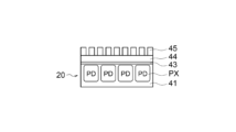
- Figures 41 to 48 are cross-sectional views illustrating an example of a manufacturing method for an image sensor 1 (particularly an image sensor 1 having a wire-grid type additional polarizer 11).
- a substrate 41 having a photodiode PD that constitutes a light-receiving pixel PX is prepared.
- the photodiode PD can be formed on the substrate 41 by any method.
- a photodiode PD can be formed for each pixel by doping a p-type Si substrate 41 by ion-implanting an n-type dopant, and activating the doped material by high-temperature annealing.
- an anti-reflection film (AR (Anti-Reflection) film) 43, a silicon dioxide film 44, and an aluminum film 45 are sequentially deposited and stacked on the substrate 41 so as to cover the photodiode PD.
- the anti-reflection film 43, the silicon dioxide film 44, and the aluminum film 45 can be stacked on the substrate 41 by any method (CVD (Chemical Vapor Deposition) is one example).
- the aluminum film 45 is processed to form an additional polarizer 11 as a wire grid type polarizer.
- the aluminum film 45 can be processed into a wire grid polarizer by any method.
- fine grooves through holes are formed in the aluminum film 45 by dry etching using a photoresist based on lithography technology (e.g., reactive ion etching (RIE)) (see Figure 43).
- RIE reactive ion etching
- a silicon dioxide film 46 is formed and laminated on the aluminum film 45 by any method (e.g., CVD), so that the fine grooves in the aluminum film 45 are filled with silicon dioxide (see Figure 44).
- an additional polarizer 11 is formed having wire lines 11a made of aluminum and inter-wire portions 11b made of silicon dioxide.
- the waveguide 30 is also formed by the silicon dioxide film 46 on the aluminum film 45.
- the polarization control unit 10 is formed on the silicon dioxide film 46 (waveguide 30).
- an amorphous silicon film 47 is formed and laminated on a silicon dioxide film 46 by any method (for example, CVD). Then, as shown in FIG. 46, a fine groove (through hole) is formed in the amorphous silicon film 47 by any method (for example, dry etching such as RIE). Then, as shown in FIG. 47, a silicon dioxide film 48 is formed and laminated on the amorphous silicon film 47 by any method (for example, CVD), so that the fine groove in the amorphous silicon film 47 is filled with silicon dioxide.
- CVD chemical etching
- a polarization control section 10 is formed with a metasurface structure having meta-atoms 10a made of amorphous silicon and a peripheral portion 10b of the structure made of silicon dioxide.
- holes are formed in the silicon dioxide film 48, the silicon dioxide filling the fine grooves of the amorphous silicon film 47 (structure peripheral portion 10b), and the silicon dioxide film 46.
- the holes can be formed by any method (e.g., dry etching such as RIE), and constitute the polarization control light shielding portion 31 (air layer).
- the image sensor 1 can be mass-produced.
- a polarization control unit 10 having a metasurface structure and a polarization splitter function is arranged as an upper layer of an additional polarizer 11 having a polarization filter function.
- the disclosed technology can be applied to various electronic devices and can be used in the general optoelectronics field (including fields related to image sensors).
- the image sensor 1 of each of the above-mentioned embodiments and modifications can be used as an imaging device included in a camera system.
- the image sensor 1 of each of the above-mentioned embodiments and modifications can also be applied to light detection devices other than imaging devices, making it possible to provide various electronic devices equipped with such light detection devices.
- Such electronic devices are capable of deriving the shape of a subject based on the detection results (including polarization information) of the light detection device (image sensor 1), and are particularly useful in situations where high sensitivity and extinction ratio are required, making it possible to detect the movement and shape of a subject with high accuracy and high speed.
- the optical detection device and electronic device disclosed herein are therefore capable of recognizing gestures made by humans based on the detection results (including polarization information), and can also be configured as a head-mounted display to detect the user's line of sight (eye movement, etc.).
- the optical detection device and electronic device disclosed herein can be applied, for example, to gaming applications, and can also be applied to VR (Virtual Reality) technology and AR (Augmented Reality) technology.
- optical detection device and electronic device disclosed herein are capable of high-speed detection of the subject shape based on the detection results (including polarization information), and therefore can be applied to cameras for industrial machinery, for example, manufacturing equipment such as product assembly systems using robots.
- the technical categories that embody the above-mentioned technical ideas are not limited.
- the above-mentioned technical ideas may be embodied by a computer program that causes a computer to execute one or more procedures (steps) included in a method of manufacturing or using the above-mentioned device.
- the above-mentioned technical ideas may also be embodied by a computer-readable non-transitory recording medium on which such a computer program is recorded.
- the present disclosure may also have the following configuration.
- a polarization control section that includes a plurality of microstructures that are two-dimensionally arranged and that selectively transmits a plurality of polarized lights in the incident light; an additional polarizer that receives the plurality of polarized lights from the polarization control unit and selectively transmits the plurality of polarized lights; a photoelectric conversion unit including a plurality of light receiving pixels that receive the plurality of polarized lights from the additional polarizer, The plurality of polarized lights transmitted through each of the polarization control unit and the additional polarizer include first polarized lights, second polarized lights, third polarized lights, and fourth polarized lights having different vibration directions from each other. Light detection device.
- the additional polarizer includes a wire grid polarizer. 3.
- the additional polarizer includes a photonic crystal polarizer. 3.
- the additional polarizer includes a plurality of additional polarization pixels and an additional polarization light shielding portion provided between adjacent additional polarization pixels; each of the plurality of additional polarization pixels selectively transmits any one of the first polarization, the second polarization, the third polarization, and the fourth polarization; 5.
- the optical detection device according to any one of items 1 to 4.
- the first polarized light and the second polarized light have vibration directions that are different by 90 degrees from each other, the third polarized light and the fourth polarized light have vibration directions that are different by 90 degrees from each other, The second polarized light and the third polarized light have vibration directions that differ by 45 degrees from each other.
- Item 6 A light detection device according to any one of items 1 to 5.
- the polarization control unit is a first unit polarization control section that selectively transmits the first polarized light and the second polarized light; a second unit polarization control section that selectively transmits the third polarized light and the fourth polarized light; Including, the additional polarizer includes a plurality of additional polarization pixels that selectively transmit any one of the first polarization, the second polarization, the third polarization, and the fourth polarization,
- the first unit polarization control section is Concentrating the first polarized light toward an additional polarization pixel that selectively transmits the first polarized light; Concentrating the second polarized light toward an additional polarization pixel that selectively transmits the second polarized light;
- the second unit polarization control section is Concentrating the third polarized light toward an additional polarization pixel that selectively transmits the third polarized light; Concentrating the fourth polarized light toward an additional polarization pixel that selectively transmits the fourth polarized light.
- a waveguide is provided between the polarization control section and the additional polarizer,
- the waveguide is a first unit polarization waveguide through which the first polarized light and the second polarized light output from the first unit polarization control section travel toward the additional polarizer;
- a second unit polarization waveguide through which the third polarized light and the fourth polarized light output from the second unit polarization control section travel toward the additional polarizer, a polarization control light shielding portion is provided between the first unit polarization waveguide and the second unit polarization waveguide adjacent to each other;
- Item 8 The optical detection device according to item 7.
- the polarization-control light shield includes a metal.
- Item 9 The optical detection device according to item 8.
- the polarization control light shielding portion includes an air layer.
- Item 9 The optical detection device according to item 8.
- the plurality of light receiving pixels have a diagonal lattice arrangement.
- the optical detection device according to any one of items 1 to 10.
- the additional polarizer includes a plurality of additional polarizing pixels having a diagonal lattice arrangement. Item 12. A light detection device according to any one of items 1 to 11.
- the polarization control unit includes a plurality of unit polarization control units having a diagonal lattice arrangement, Item 13.
- a light detection device according to any one of items 1 to 12.
- a polarization control section that includes a plurality of microstructures that are two-dimensionally arranged and that selectively transmits a plurality of polarized lights in the incident light; an additional polarizer that receives the plurality of polarized lights from the polarization control unit and selectively transmits the plurality of polarized lights; a photoelectric conversion unit including a plurality of light receiving pixels that receive the plurality of polarized lights from the additional polarizer; An electronic device comprising a photodetector, wherein the plurality of polarized lights passing through each of the polarization control unit and the additional polarizer include a first polarized light, a second polarized light, a third polarized light and a fourth polarized light having mutually different vibration directions.
- the additional polarizer includes a wire grid polarizer.
- Item 16 The electronic device according to item 14 or 15.
- the additional polarizer includes a photonic crystal polarizer.
- Item 16 The electronic device according to item 14 or 15.
- the additional polarizer includes a plurality of additional polarization pixels and an additional polarization light shielding portion provided between adjacent additional polarization pixels; each of the plurality of additional polarization pixels selectively transmits any one of the first polarization, the second polarization, the third polarization, and the fourth polarization; Item 18.
- An electronic device according to any one of items 14 to 17.
- the first polarized light and the second polarized light have vibration directions that are different by 90 degrees from each other, the third polarized light and the fourth polarized light have vibration directions that are different by 90 degrees from each other, The second polarized light and the third polarized light have vibration directions that differ by 45 degrees from each other.
- An electronic device according to any one of items 14 to 18.
- the polarization control unit is a first unit polarization control section that selectively transmits the first polarized light and the second polarized light; a second unit polarization control section that selectively transmits the third polarized light and the fourth polarized light; Including, the additional polarizer includes a plurality of additional polarization pixels that selectively transmit any one of the first polarization, the second polarization, the third polarization, and the fourth polarization,
- the first unit polarization control section is Concentrating the first polarized light toward an additional polarization pixel that selectively transmits the first polarized light; Concentrating the second polarized light toward an additional polarization pixel that selectively transmits the second polarized light;
- the second unit polarization control section is Concentrating the third polarized light toward an additional polarization pixel that selectively transmits the third polarized light; Concentrating the fourth polarized light toward an additional polarization pixel that selectively transmits the fourth polarized light.
- a waveguide is provided between the polarization control section and the additional polarizer,
- the waveguide is a first unit polarization waveguide through which the first polarized light and the second polarized light output from the first unit polarization control section travel toward the additional polarizer;
- a second unit polarization waveguide through which the third polarized light and the fourth polarized light output from the second unit polarization control section travel toward the additional polarizer, a polarization control light shielding portion is provided between the first unit polarization waveguide and the second unit polarization waveguide adjacent to each other;
- the polarization-control light shield includes a metal. 22. The electronic device according to item 21.
- the polarization control light shielding portion includes an air layer. 22. The electronic device according to item 21.
- the plurality of light receiving pixels have a diagonal lattice arrangement.
- Item 24 An electronic device according to any one of items 14 to 23.
- the additional polarizer includes a plurality of additional polarizing pixels having a diagonal lattice arrangement. Item 25. An electronic device according to any one of items 14 to 24.
- the polarization control unit includes a plurality of unit polarization control units having a diagonal lattice arrangement, Item 26.
- An electronic device according to any one of items 14 to 25.
Landscapes
- Physics & Mathematics (AREA)
- General Physics & Mathematics (AREA)
- Optics & Photonics (AREA)
- Solid State Image Pick-Up Elements (AREA)
- Polarising Elements (AREA)
Abstract
[課題]各受光画素において、所望の偏光の良好な受光感度を実現しつつ、望まれない偏光の受光を抑えるのに有利な技術を提供する。 [解決手段]光検出装置は、二次元的に配列される複数の微細構造体を含み、入射光中の複数の偏光を選択的に透過する偏光制御部と、偏光制御部からの複数の偏光が入射し、当該複数の偏光を選択的に透過する追加偏光子と、追加偏光子からの複数の偏光を受光する複数の受光画素を含む光電変換部と、を備え、偏光制御部及び追加偏光子の各々を透過する複数の偏光は、お互いに振動方向が異なる第1偏光、第2偏光、第3偏光及び第4偏光を含む。
Description
本開示は、光検出装置及び電子機器に関する。
偏光子を具備する偏光イメージセンサ(光検出装置)は、明るさ及び色の情報に加え、偏光子を具備しないイメージセンサでは感知できない偏光情報を得ることができ、そのような偏光情報から被写体の形状を把握することも可能である。そのため偏光イメージセンサは、偏光子を具備しないイメージセンサから出力される画像では可視化や認識が困難であった対象の検査等に応用が可能であり、今後も様々な産業機器分野での活用が期待される。
特許文献1は、ワイヤーグリッド型偏光子及び光電変換素子を備える固体撮像素子を開示する。
近年、メタサーフェスとも呼ばれる多数の微細構造体を含む偏光子が注目されている。メタサーフェス構造の偏光子を具備する偏光イメージセンサは、優れた偏光受光感度を示す傾向がある。
例えば特許文献1の固体撮像素子では、入射光のうちワイヤーグリッド型偏光子を透過した偏光波が光電変換素子(受光画素)に入射して受光される。しかしながらワイヤーグリッド型偏光子は、入射光のうち所望方向に振動する偏光のみを透過し、他の方向に振動する偏光を遮断するため、光学的なロスが大きく低光透過率を示す。その結果、ワイヤーグリッド型偏光子を具備する固体撮像素子は低感度及び低消光比を示す傾向がある。
一方、メタサーフェス構造の偏光子は、ワイヤーグリッド型偏光子に比べ、優れた光透過率を示す傾向がある。
ただしメタサーフェス構造の偏光子は、所望方向に振動する偏光を受光することが意図された受光画素に向けた、当該所望方向とは異なる方向に振動する偏光の出射を十分に抑えることが難しい場合がある。その結果、メタサーフェス構造の偏光子を具備する偏光イメージセンサでは、各受光画素が、所望方向に振動する偏光だけではなく当該所望方向とは異なる方向に振動する偏光も受光することになり、良好な消光比を実現することが簡単ではない。
本開示は、各受光画素において、所望の偏光の良好な受光感度を実現しつつ、望まれない偏光の受光を抑えるのに有利な技術を提供する。
本開示の一態様は、二次元的に配列される複数の微細構造体を含み、入射光中の複数の偏光を選択的に透過する偏光制御部と、偏光制御部からの複数の偏光が入射し、当該複数の偏光を選択的に透過する追加偏光子と、追加偏光子からの複数の偏光を受光する複数の受光画素を含む光電変換部と、を備え、偏光制御部及び追加偏光子の各々を透過する複数の偏光は、お互いに振動方向が異なる第1偏光、第2偏光、第3偏光及び第4偏光を含む、光検出装置に関する。
偏光制御部は、複数の偏光の各々を、追加偏光子のうちの互いに異なる領域に向けて集光してもよい。
追加偏光子は、ワイヤーグリッド型偏光子を含んでもよい。
追加偏光子は、フォトニック結晶型偏光子を含んでもよい。
追加偏光子は、複数の追加偏光画素と、隣り合う追加偏光画素間に設けられる追加偏光遮光部と、を含んでもよく、複数の追加偏光画素の各々は、第1偏光、第2偏光、第3偏光及び第4偏光のうちのいずれかを選択的に透過してもよい。
第1偏光及び第2偏光は、お互いに90度異なる振動方向を有してもよく、第3偏光及び第4偏光は、お互いに90度異なる振動方向を有してもよく、第2偏光及び第3偏光は、お互いに45度異なる振動方向を有してもよい。
偏光制御部は、第1偏光及び第2偏光を選択的に透過する第1単位偏光制御部と、第3偏光及び第4偏光を選択的に透過する第2単位偏光制御部と、を含んでもよく、追加偏光子は、第1偏光、第2偏光、第3偏光及び第4偏光のうちのいずれかを選択的に透過する複数の追加偏光画素を含んでもよく、第1単位偏光制御部は、第1偏光を選択的に透過する追加偏光画素に向けて第1偏光を集光し、第2偏光を選択的に透過する追加偏光画素に向けて第2偏光を集光してもよく、第2単位偏光制御部は、第3偏光を選択的に透過する追加偏光画素に向けて第3偏光を集光し、第4偏光を選択的に透過する追加偏光画素に向けて第4偏光を集光してもよい。
光検出装置は、偏光制御部と追加偏光子との間に設けられる導波路を備えてもよく、導波路は、第1単位偏光制御部から出射する第1偏光及び第2偏光が追加偏光子に向かって進行する第1単位偏光導波路と、第2単位偏光制御部から出射する第3偏光及び第4偏光が追加偏光子に向かって進行する第2単位偏光導波路と、を有してもよく、隣り合う第1単位偏光導波路と第2単位偏光導波路との間に偏光制御遮光部が設けられてもよい。
偏光制御遮光部は金属を含んでもよい。
偏光制御遮光部はエア層を含んでもよい。
複数の受光画素は斜め格子配列を有してもよい。
追加偏光子は、斜め格子配列を有する複数の追加偏光画素を含んでもよい。
偏光制御部は、斜め格子配列を有する複数の単位偏光制御部を含んでもよい。
本開示の他の態様は、上記のいずれかの光検出装置を備える電子機器に関する。
図面を参照して本開示技術の例示的な実施形態を説明する。以下では、カメラシステムなどに応用可能なイメージセンサ(固体撮像素子)に対し、本開示技術が適用されるケースについて説明する。ただし本開示技術の適用対象は限定されず、撮像以外の用途にも応用可能な他の光検出装置(例えばセンサ等)に本開示技術が適用されてもよい。
なお図面中の各要素は模式的又は概念的に示されている。したがって図面中の各要素のサイズ及び形状等の特性は、現実の対応の要素の特性とは異なりうる。また図面中の要素間のサイズ比も、現実の装置における対応要素間のサイズ比とは異なりうる。また図面間で、各要素のサイズ及び形状や要素間のサイズ比は必ずしも一致せず、各図面において特定の1又は複数の要素が誇張されて表現されていることもある。
以下の説明において、X方向、Y方向及びZ方向はお互いに直交する方向である。例えばX方向が水平方向に対応してもよく、Y方向は垂直方向(高さ方向)に対応してもよく、Z方向が奥行き方向に対応してもよい。
図1は、イメージセンサ1の構成例を示す概略図である。図1において、偏光制御部(偏光スプリッター)10、追加偏光子11及び光電変換部20は斜めから見た状態で示されており、光学系OPは側方から見た状態が示されている。
イメージセンサ1は、典型的にはCCD(Charge Coupled Device)イメージセンサ又はCMOS(Complementary Metal Oxide Semiconductor)イメージセンサによって構成可能である。ただしイメージセンサ1は、任意の撮像デバイスによって構成可能である。
イメージセンサ1は、外部にある被写体からの光を受光し、当該光の強度情報及び色情報を含む各種情報に関するデータを取得して、被写体の画像を生成する。被写体からの光の偏光情報には、光強度及び色(波長)のみからでは取得できない有益な情報が含まれており、例えば被写体の表面の形状に関する情報や被写体の材料に関する情報が含まれうる。このような偏光情報を用いる偏光イメージング技術は、車載用カメラ、IoT(Internet of Things)デバイス及び医療用デバイス等、様々な分野で活用可能である。
図1に示すイメージセンサ1は、光学系OP、偏光制御部10、追加偏光子11及び光電変換部20を備える。光学系OPは、被写体からの入射光Lを集光するレンズ等を含む。光学系OPを通過した入射光Lは、主光線の光軸方向に進行する正面入射光Laと、主光線の光軸に対して傾斜する方向に進行する傾斜入射光Lbとを含む。図1に示す例では、光軸方向がZ方向に一致する。
光電変換部20は、入射光L(特に入射光Lから取り出される複数の偏光)を受光する複数の受光画素PXを含む。図1に示す例では、複数の受光画素PXがX方向及びY方向に二次元的に並べられており、光電変換部20は、全体としてX方向及びY方向に延びる辺を持つ矩形状を有する。光電変換部20の中央部(像高0割)に位置する受光画素PXは、正面入射光Laを受光する。光電変換部20の中央部から離れて位置する受光画素PX(例えば光電変換部20の端部(例えば像高10割)に位置する受光画素PX)は、傾斜入射光Lbを受光する。
各受光画素PXは、Si(シリコン)半導体材料等のフォトダイオードを有する。なお各受光画素PXは、入射光(偏光)の波長(例えば940nm)に応じて入射光の吸収率(感度)が変わりうるため、各受光画素PXの光吸収係数は必ずしも大きくない。そのため、一例として、各受光画素PXの表面(受光面)に光散乱体(図示省略)を設置して当該光散乱体によって入射光を散乱させることで、各受光画素PXにおける入射光の光路長を増大させて各受光画素PXの感度を向上させてもよい。
偏光制御部10及び追加偏光子11は、光学系OPと光電変換部20との間の光路に配置され、光電変換部20の複数の受光画素PX(特に受光面)を覆うように設けられる。偏光制御部10は、「メタアトム」とも呼ばれる多数(複数)の微細構造体を含むメタサーフェス構造を有する。一方、追加偏光子11は、メタサーフェス構造を持たない偏光子である。追加偏光子11として、入射光Lから所望の直線偏光を取り出すことができる任意構造の偏光子(例えば後述のワイヤーグリッド型偏光子やフォトニック結晶型偏光子)を用いることが可能である。
偏光制御部10及び追加偏光子11のうち光電変換部20の中央部に位置する受光画素PXを覆う部分は、正面入射光Laの偏光制御を行って、正面入射光La(特に偏光成分)を光電変換部20の中央部に位置する受光画素PX上に集光させる。偏光制御部10及び追加偏光子11のうち光電変換部20の端部に位置する受光画素PXを覆う部分は、傾斜入射光Lbの偏光制御を行って、傾斜入射光Lb(特に偏光成分)を光電変換部20の端部に位置する受光画素PX上に集光させる。このように偏光制御部10及び追加偏光子11の各部分は、様々な角度で入射する入射光Lに含まれる特定の偏光成分を選択的に通過させて対応の受光画素PX上に集光させる。
追加偏光子11は、光軸方向に関して偏光制御部10と光電変換部20との間に設けられ、偏光制御部10からの複数の偏光が入射し、当該複数の偏光を選択的に透過する。特に偏光制御部10は、後述のように、複数の偏光を、それぞれ追加偏光子11のうちの互いに異なる領域(後述の「複数の追加偏光画素」)に向けて集光する。光電変換部20が有する複数の受光画素PXは、追加偏光子11から選択的に出射される複数の偏光を受光する。各受光画素PXには、所望方向に振動する偏光が選択的に入射するように、偏光制御部10(特に後述の単位偏光制御部)及び追加偏光子11(特に後述の追加偏光画素)が割り当てられる。
本例において、偏光制御部10及び追加偏光子11の各々を透過し且つ光電変換部20によって受光される複数の偏光は、お互いに振動方向が異なる第1偏光、第2偏光、第3偏光及び第4偏光を含む。
第1偏光~第4偏光の具体的な振動方向は限定されない。典型的には、イメージセンサ1に入射する直前の入射光Lにおいて、第1偏光及び第2偏光はお互いに90度異なる振動方向を有し、第3偏光及び第4偏光はお互いに90度異なる振動方向を有し、第2偏光及び第3偏光はお互いに45度異なる振動方向を有する。後述の各実施形態では、第1偏光~第4偏光がそれぞれ、伝播方向を基準に0度(degree)、+90度、-45度及び+45度の振動方向を有する。例えばXY平面において、0度の振動方向はX方向に一致する方向であってもよく、+90度の振動方向はY方向に一致する方向であってもよく、-45度及び+45度の振動方向はX方向及びY方向に対して斜めを成す方向であってもよい。
上述のイメージセンサ1(特に偏光制御部10及び追加偏光子11)は様々な構成をとりうる。以下、イメージセンサ1の典型的な実施形態について説明する。
[第1実施形態]
本実施形態の追加偏光子11は、ワイヤーグリッド型偏光子を含む。
本実施形態の追加偏光子11は、ワイヤーグリッド型偏光子を含む。
図2A及び図2Bは、第1実施形態の第1の例のイメージセンサ1の概略を示す部分断面図(XZ断面図)であり、入射光Lがイメージセンサ1(特に偏光制御部10)に対して垂直に入射する場合を示す。特に、図2Aは第1受光画素PX1及び第2受光画素PX2を示し、図2Bは第3受光画素PX3及び第4受光画素PX4を示す。図3は、第1実施形態の第1の例の偏光制御部10(特に偏光制御ユニット)の概略を示す平面図である。図4は、第1実施形態の第1の例の追加偏光子11(特に追加偏光画素ユニット)の概略を示す平面図である。
図5は、単位偏光制御部10gの一例を示す偏光制御部10(特に偏光制御ユニット)の平面図である。図6は、図4に示す追加偏光子11の追加偏光画素11gと、割り当てられる偏光の振動方向P1~P4との対応関係を示す追加偏光子11(特に追加偏光画素ユニット)の平面図である。図7は、図2Aに示すイメージセンサ1において偏光制御部10から出射した第1偏光Lp1(振動方向P1=0度)の進行方向を示す部分断面図である。図8は、図2Aに示すイメージセンサ1において偏光制御部10から出射した第2偏光Lp2(振動方向P2=90度)の進行方向を示す部分断面図である。
図2A~図8に示す例では、偏光制御部10、追加偏光子11及び光電変換部20の各々が正方画素配列を有する。
すなわちX方向に2つの受光画素PXが並び且つY方向に2つの受光画素PXが並ぶ正方格子配列の4つの受光画素PXを1つの受光画素ユニットとし、当該受光画素ユニットがX方向及びY方向に複数並べられる。各受光画素ユニットに含まれる4つの受光画素PX(第1受光画素PX1~第4受光画素PX4)は、それぞれ第1偏光Lp1~第4偏光Lp4に割り当てられる(図2A及び図2B参照)。
具体的には、各受光画素ユニットのうちX方向に並べられる第1受光画素PX1及び第2受光画素PX2(図2A参照)は、それぞれ第1偏光Lp1(振動方向P1=0度)及び第2偏光Lp2(振動方向P2=90度)を受光するための受光画素PXである。各受光画素ユニットのうちX方向に並べられる他の第3受光画素PX3及び第4受光画素PX4(図2B参照)は、それぞれ第3偏光Lp3(振動方向P3=-45度)及び第4偏光Lp4(振動方向P4=+45度)を受光するための受光画素PXである。
このように4方向に振動する偏光を分離して受光可能なイメージセンサ1によって取得される偏光情報の位相によれば、被写体表面の法線ベクトルを推定することができ、ひいては被写体の形状を把握することが可能である。
ワイヤーグリッド型偏光子である追加偏光子11は多数のワイヤー線11aを含む(図4参照)。各ワイヤー線11aは、例えばアルミニウム(Al)等の金属によって構成されるが、他の材料によって構成されてもよい。
隣り合うワイヤー線11a間のワイヤー間部分11bは偏光透過領域であり、空間(エア領域)として構成されてもよいし、低屈折率材料(例えば二酸化ケイ素(SiO2))によって構成されてもよい。
追加偏光子11は、図4に示すように複数の追加偏光画素11gに区分される。本例の追加偏光子11に含まれる複数の追加偏光画素11gは、正方格子配列を有する。
すなわちX方向に2つの追加偏光画素11gが並び且つY方向に2つの追加偏光画素11gが並ぶ正方格子配列の4つの追加偏光画素11gを1つの追加偏光画素ユニットとして、当該追加偏光画素ユニットがX方向及びY方向に複数並べられる。各追加偏光画素ユニットに含まれるこれらの4つの追加偏光画素11gは、それぞれ第1偏光Lp1~第4偏光Lp4に割り当てられる。
具体的には図6に示すように、各追加偏光画素ユニットのうちX方向に並べられる第1追加偏光画素11g1及び第2追加偏光画素11g2は、それぞれ第1偏光Lp1(振動方向P1=0度)及び第2偏光(振動方向P2=90度)を選択的に透過する。一方、各追加偏光画素ユニットのうちX方向に並べられる他の第3追加偏光画素11g3及び第4追加偏光画素11g4は、それぞれ第3偏光Lp3(振動方向P3=-45度)及び第4偏光Lp4(振動方向P4=+45度)を選択的に透過する。
このように各追加偏光画素11gは、第1偏光Lp1、第2偏光Lp2、第3偏光Lp3及び第4偏光Lp4のうちのいずれかを選択的に透過する。なお各追加偏光画素11gのワイヤー線11aの延在方向は、割り当てられる偏光の振動方向に応じて定められ、割り当てられる偏光の振動方向に対して90度を成す方向である(図6参照)。
追加偏光子11は、更に、各追加偏光画素11gを囲むように設けられる枠状の追加偏光遮光部11c(図4参照)を有する。追加偏光遮光部11cは、光(特に偏光)の透過を遮ることができる任意の構成及び任意の組成を有する。したがって追加偏光遮光部11cは、光を反射することで遮光するように構成されてもよいし、光を吸収することで遮光するように構成されてもよい。
このようにして隣り合う追加偏光画素11g間に設けられる追加偏光遮光部11cは、隣り合う追加偏光画素11g間における光(特に偏光)の漏れ出し(クロストーク)を抑えることができ、高い消光比を得るのに有利である。
メタサーフェス構造の偏光制御部10は、図2A及び図2に示すように、入射光Lの入射方向A0に関して追加偏光子11よりも上流側に設けられる。この偏光制御部10は、入射光L中の複数の偏光(第1偏光Lp1~第4偏光Lp4)を選択的に透過しつつ分離する偏光スプリッター機能を発揮する。
本例では、偏光制御部10と光電変換部20(各受光画素PX)との間に導波路30が設けられる。導波路30は任意の構成を有することができ、導波路30を構成可能な材料は限定されない。例えばアモルファスシリコン、多結晶シリコン、ゲルマニウム、酸化チタン、酸化ニオブ、酸化タンタル、酸化アルミニウム、酸化ハフニウム、窒化シリコン、酸化シリコン、窒化酸化シリコン、炭化シリコン、酸化炭化シリコン、窒化炭化シリコン及び酸化ジルコニウムのうちのいずれかの透明材料によって、導波路30が作られてもよい。
偏光制御部10に含まれる複数のメタアトム(微細構造体)10aは、図3に示すようにX方向及びY方向へ二次元的に配列されており、受光画素PX(光電変換部20)の受光面に対して略平行な面内に配置される。各メタアトム10aの屈折率は、メタアトム10a間の領域(すなわち構造体周辺部10b)の屈折率よりも大きい。
メタアトム10aは任意の構成を有することができ、各メタアトム10aを構成可能な材料は限定されない。例えばアモルファスシリコン(α-Si)、多結晶シリコン(Poly-Si)、ゲルマニウム、酸化チタン(TiO2)、酸化ニオブ、酸化タンタル、酸化アルミニウム、酸化ハフニウム、窒化シリコン(SiN、Si3N4)、酸化シリコン、窒化酸化シリコン、炭化シリコン、酸化炭化シリコン、窒化炭化シリコン、酸化ジルコニウム、窒化ガリウム(GaN)、ヒ化ガリウム(GaAs)及びリン化イジウム(InP)のうちのいずれかによって、各メタアトム10aが作られてもよい。
またメタアトム10a間の領域(構造体周辺部10b)は任意の構成を有することができ、例えば空間として設けられてもよいし、二酸化ケイ素などの実体材料によって構成されてもよい。
なおメタアトム10a及び導波路30は、お互いに異なる材料で作られる。例えば、導波路30がシリコン酸化膜又は酸化チタンで作られる場合、メタアトム10aは、シリコン単結晶又はアモルファスシリコンで作られてもよい。ただし構造体周辺部10bは、導波路30とは異なる材料で構成されてもよいし、導波路30と同じ材料で構成されてもよい。
各メタアトム10aは、ピラー形状を有し、理想的には矩形の断面形状及び平面形状を有する直方体として構成される。ただし実際には、リソグラフィのフォトマスクを使った加工で偏光制御部10を作製すると、各メタアトム10aの角部が丸味を帯びることがある。各メタアトム10aの角部が丸味を帯びていても、偏光制御部10は偏光スプリッター機能を十分に発揮しうる。このように各メタアトム10aの形状は限定されず、各メタアトム10aの断面形状及び平面形状は、任意の多角形、楕円形、中空形、又はそれ以外の形状であってもよい。
偏光制御部10は、お互いに異なる方向に振動する偏光を分離及び出射(集光)する複数種類の単位偏光制御部10gを含む(図5参照)。
本例の各単位偏光制御部10gは、2つの受光画素PXに対応する範囲(すなわち2つの受光画素PXを覆う領域)に設けられ、入射光L中の2つの偏光成分をお互い異なる方向に選択的に出射して集光する。これにより各単位偏光制御部10gは、入射光Lのうち2画素(複数画素)に対応する範囲に入射した偏光を、1画素(単一画素)に対応する追加偏光子11(追加偏光画素11g)及び光電変換部20(受光画素PX)に集中させることができる。
具体的には、複数の単位偏光制御部10gは第1単位偏光制御部10g1及び第2単位偏光制御部10g2を含む。すなわちY方向に隣り合う1つの第1単位偏光制御部10g1及び1つの第2単位偏光制御部10g2を1つの偏光制御ユニットとして、当該偏光制御ユニットがX方向及びY方向に複数並べられる。
第1単位偏光制御部10g1は、第1追加偏光画素11g1及び第2追加偏光画素11g2に割り当てられ、ひいては第1受光画素PX1及び第2受光画素PX2に割り当てられる。第2単位偏光制御部10g2は、第3追加偏光画素11g3及び第4追加偏光画素11g4に割り当てられ、ひいては第3受光画素PX3及び第4受光画素PX4に割り当てられる。
各第1単位偏光制御部10g1に含まれる複数のメタアトム10aは、入射光L中の第1偏光Lp1の振動方向P1(0度:X方向)及び第2偏光Lp2の振動方向P2(90度:Y方向)の各々に沿って直線的に配列される。各第1単位偏光制御部10g1の複数のメタアトム10aは、入射光L中の第1偏光Lp1の振動方向P1(X方向)及び第2偏光Lp2の振動方向P2(Y方向)のサイズが互いに異なる複数のメタアトム10aを含む。
各第2単位偏光制御部10g2の複数のメタアトム10aは、第3偏光Lp3の振動方向P3(-45度)及び第4偏光Lp4の振動方向P4(+45度)に沿って直線的に配列され、当該振動方向P3、P4のサイズが互いに異なる複数のメタアトム10aを含む。
複数のメタアトム10aが上述の構造を有することで、各単位偏光制御部10gは、入射光L中の偏光成分を追加偏光子11(特に対応の追加偏光画素11g)に向けて選択的に出射(集光)する。
すなわち図2Aに示すように第1単位偏光制御部10g1は、入射光L中の第1偏光Lp1及び第2偏光Lp2を選択的に透過し、第1偏光Lp1を第1追加偏光画素11g1に向けて出射(集光)しつつ、第2偏光Lp2を第2追加偏光画素11g2に向けて出射(集光)する。なお図2Aにおいて第1単位偏光制御部10g1から第1追加偏光画素11g1に向かう第1偏光Lp1の進行方向が「A1」によって表される。また第1単位偏光制御部10g1から第2追加偏光画素11g2に向かう第2偏光Lp2の進行方向が「A2」によって表される。
図7に示すように、第1単位偏光制御部10g1のうち第1受光画素PX1を覆う部分から出射される第1偏光Lp1は、Z方向に沿って又はZ方向に対して僅かに傾斜する斜め方向に沿って、第1受光画素PX1に向かって進行する。第1単位偏光制御部10g1のうち第2受光画素PX2を覆う部分から出射される第1偏光Lp1は、Z方向に対して大きく傾斜する斜め方向(図7の左下方向)に沿って、第1受光画素PX1に向かって進行する。
一方、図8に示すように、第1単位偏光制御部10g1のうち第2受光画素PX2を覆う部分から出射される第2偏光Lp2は、Z方向に沿って又はZ方向に対して僅かに傾斜する斜め方向に沿って、第2受光画素PX2に向かって進行する。第1単位偏光制御部10g1のうち第1受光画素PX1を覆う部分から出射される第2偏光Lp2は、Z方向に対して大きく傾斜する斜め方向(図8の右下方向)に沿って、第2受光画素PX2に向かって進行する。
同様に、図2Bに示すように第2単位偏光制御部10g2は、第3偏光Lp3及び第4偏光Lp4を選択的に透過し、第3偏光Lp3を第3追加偏光画素11g3に向けて出射(集光)しつつ、第4偏光Lp4を第4追加偏光画素11g4に向けて出射(集光)する。なお図2Bにおいて第2単位偏光制御部10g2から第3追加偏光画素11g3に向かう第3偏光Lp3の進行方向が「A3」によって表される。また第2単位偏光制御部10g2から第4追加偏光画素11g4に向かう第4偏光Lp4の進行方向が「A4」によって表される。
上述の構成を有するイメージセンサ1によれば、偏光制御部10によって、追加偏光子11のそれぞれの追加偏光画素11gに対して対応の所望の偏光を集光することができる。その結果、各追加偏光画素11gに対する望まれない偏光の入射を抑えることができ、追加偏光子11における光のロスを効果的に低減できる。
また各追加偏光画素11gは、所望の偏光の透過を許容しつつ、望まれない偏光の透過を効果的に防ぐ。
したがって本例のイメージセンサ1は、各受光画素PXにおいて所望の偏光の良好な受光感度を確保しつつ、望まれない偏光の受光を抑えることができ、高い消光比を実現するのに有利である。
なおイメージセンサ1は、上述の図2A~図8に示す構成とは異なる構成を、適宜とりうる。
図9は、追加偏光子11の一変形例の概略を示す平面図である。
より効果的にクロストークを抑える観点からは、隣り合う追加偏光画素11gの実質的な透光エリア(ワイヤー間部分11b)間の距離が大きくなるように、追加偏光子11の追加偏光遮光部11cが設けられることが好ましい。図9に示す例では、各追加偏光画素11gの実質的な透光エリア(ワイヤー間部分11b)が、各画素の中央において円形の平面形状を有するように、追加偏光遮光部11cが設けられる。
このように追加偏光遮光部11cが、各追加偏光画素11gにおける光(特に偏光)を透過可能な透光エリアを制限する絞りとして設けられることで、各受光画素PXへの望まれない偏光の入射が抑えられ、ひいては消光比を向上させることができる。
次に、上述の図1~図8に示す構造を有するイメージセンサ1を使って行ったFDTD法(Finite-Difference Time-Domain method)の波動シミュレーションの結果例について述べる。
[第1のシミュレーション結果]
本シミュレーションでは、図1~図8に示す構造を有するイメージセンサ1に対し、波長940nmの入射光L(特に第1偏光Lp1(すなわち第2偏光Lp2~第4偏光Lp4を含まず第1偏光Lp1のみを含む入射光L))を垂直に入射させた。
本シミュレーションでは、図1~図8に示す構造を有するイメージセンサ1に対し、波長940nmの入射光L(特に第1偏光Lp1(すなわち第2偏光Lp2~第4偏光Lp4を含まず第1偏光Lp1のみを含む入射光L))を垂直に入射させた。
図10は、光電変換部20(特に第1受光画素PX1~第4受光画素PX4を含む受光画素ユニットPXg)におけるFDTD法の波動シミュレーションの結果の一例(受光パワー分布)を示す図である。図10に示す受光画素ユニットPXgにおいて、白に近い色で表される箇所ほど第1偏光Lp1を強く受光していることを示し、黒に近い色で表される箇所ほど第1偏光Lp1の受光強度が弱いことを示す。
図10に示す結果例では、第1受光画素PX1が第1偏光Lp1を相対的に強く受光しており、他の受光画素PX(とりわけ第2受光画素PX2)による第1受光画素PX1の受光強度は相対的に弱かった。
上述のように第1偏光Lp1は、偏光制御部10(特に第1単位偏光制御部10g1)によって第1追加偏光画素11g1に集光され、第1追加偏光画素11g1を透過して第1受光画素PX1に集中的に入射するように誘導される。すなわち第1偏光Lp1は、第1追加偏光画素11g1以外の追加偏光画素11gに入射しないように、ひいては第1受光画素PX1以外の受光画素PXに本来的に入射しないように、偏光制御部10によって誘導される。
図10に示すシミュレーション結果は、そのような図1~図8のイメージセンサ1の構造的特性にも合致しており、第1偏光Lp1を第1受光画素PX1によって選択的に集中して受光させるのに図1~図8に示すイメージセンサ1が有利なことを裏付ける。
なお図10は第1偏光Lp1に関するシミュレーション結果を示すが、他の偏光(第2偏光Lp2~第4偏光Lp4)についても同様のシミュレーション結果が得られた。すなわち図1~図8に示すイメージセンサ1が、第2偏光Lp2~第4偏光Lp4をそれぞれ第2受光画素PX2~第4受光画素PX4によって選択的に集中して受光させるのに有利なことが、シミュレーション結果によって裏付けられた。
[第2のシミュレーション結果]
本件発明者は、偏光制御部10及び追加偏光子11の有無に基づくシミュレーションも行った。すなわち「偏光制御部10及び追加偏光子11を具備するイメージセンサ1」及び「偏光制御部10及び追加偏光子11のうちの一方のみを具備する(他方を具備しない)イメージセンサ1」に基づくシミュレーションも行った。
本件発明者は、偏光制御部10及び追加偏光子11の有無に基づくシミュレーションも行った。すなわち「偏光制御部10及び追加偏光子11を具備するイメージセンサ1」及び「偏光制御部10及び追加偏光子11のうちの一方のみを具備する(他方を具備しない)イメージセンサ1」に基づくシミュレーションも行った。
ここで「偏光制御部10及び追加偏光子11を具備するイメージセンサ1」は、上述の図1~図8に示す構造を有する。一方、「偏光制御部10及び追加偏光子11のうちの一方のみを具備するイメージセンサ1」は、上述の図1~図8に示す構造から偏光制御部10又は追加偏光子11が取り除かれた構造を有する。
偏光制御部10及び追加偏光子11以外の構成は、シミュレーションを行ったイメージセンサ1間で共通させた。
下記の表1は、「偏光制御部10及び追加偏光子11を具備するイメージセンサ1」及び「偏光制御部10及び追加偏光子11のうちの一方のみを具備するイメージセンサ1」に基づいて行われたシミュレーションの結果例を示す。
本シミュレーションでは、イメージセンサ1に対し、同じ光強度を有する波長940nmの入射光L(特に第1偏光Lp1(すなわち第2偏光Lp2~第4偏光Lp4を含まず第1偏光Lp1のみを含む入射光L))を垂直に入射させた。
上記の表1において「第1受光画素の受光パワー」及び「第2受光画素の受光パワー」は、それぞれ第1受光画素PX1及び第2受光画素PX2による第1偏光Lp1の受光強度を示す数値である。「第1受光画素の受光パワー」の数値が大きいほど、各受光画素PXにおける所望の偏光の受光感度(本例では第1受光画素PX1における第1偏光Lp1の受光感度)が高いことを示し、通常は望ましい。一方、「第2受光画素の受光パワー」の数値が大きいほど、各受光画素PXにおける望まれない偏光の受光感度(本例では第2受光画素PX2における第1偏光Lp1の受光感度)が高いことを示し、通常は望ましくない。
また上記の表1において「消光比」は、「第1受光画素の受光パワー」及び「第2受光画素の受光パワー」の比を示す(消光比=第1受光画素の受光パワー/第2受光画素の受光パワー)。消光比の値が大きいほど、各受光画素PXにおける所望の偏光の受光感度が高く且つ望まれない偏光の受光感度が低いことを示す。
表1の結果から、偏光制御部10が設けられ且つ追加偏光子11が設けられない場合(番号「1」参照)、第1偏光Lp1に対し、第1受光画素PX1の受光パワーは大きいが、第2受光画素PX2の受光パワーも大きい。その結果、偏光制御部10が設けられ且つ追加偏光子11が設けられない場合には、相対的に高い消光比が得られないことが分かる。
また表1の結果から、偏光制御部10が設けられず且つ追加偏光子11が設けられる場合(番号「2」参照)、第1受光画素PX1の受光パワーが相対的に小さい。したがって追加偏光子11を通過して第1受光画素PX1に到達する第1偏光Lp1の強度が本来的に弱く、結果的にイメージセンサ1が低感度になることが分かる。その結果、偏光制御部10が設けられず且つ追加偏光子11が設けられる場合にも、相対的に高い消光比が得られないことが分かる。
一方、表1の結果から、偏光制御部10及び追加偏光子11が設けられる場合(番号「3」参照)、第1偏光Lp1に対し、第1受光画素PX1の受光パワーの確保及び第2受光画素PX2の受光パワーの低減がバランス良く両立される。
例えば、追加偏光子11のみが設けられる場合(番号「2」)に比べ、偏光制御部10及び追加偏光子11が設けられる場合(番号「3」)には第1偏光Lp1に対する第1受光画素PX1の受光パワーが約3倍増大した。また追加偏光子11のみが設けられる場合(番号「2」)に比べ、偏光制御部10及び追加偏光子11が設けられる場合(番号「3」)には第1偏光Lp1に対する第2受光画素PX2の受光パワーが約1/5に低減した。
その結果、追加偏光子11のみが設けられる場合(番号「2」)に比べ、偏光制御部10及び追加偏光子11が設けられる場合(番号「3」)には消光比が約12倍増大した。また偏光制御部10のみが設けられる(番号「1」)に比べ、偏光制御部10及び追加偏光子11が設けられる場合(番号「3」)には消光比が約204倍増大した。
上述の表1の結果からも、イメージセンサ1は偏光制御部10及び追加偏光子11を具備することで、各受光画素PXに関して「所望の偏光に対する高い感度」且つ「望ましくない偏光に対する低い感度」を実現して桁違いの高い消光比を得られることが分かる。したがって本実施形態のイメージセンサ1の出力結果によれば、より正確な偏光の位相見積もりを得ることが可能であり、ひいてはより高精度な被写体表面の法線ベクトル見積もりや形状把握が可能になる。
次に、第1実施形態の他の例について説明する。
図11は、第1実施形態の第2の例の偏光制御部10(特に偏光制御ユニット)の概略を示す平面図である。図12は、第1実施形態の第2の例の追加偏光子11(特に追加偏光画素ユニット)の概略を示す平面図である。
第2の例では、光電変換部20の各受光画素ユニットPXgにおける第3受光画素PX3及び第4受光画素PX4の配置が、上述の第1の例における配置(図10参照)と入れ替わっている。すなわち第1受光画素PX1に対してY方向に隣り合うように第4受光画素PX4が配置され、第2受光画素PX2に対してY方向に隣り合うように第3受光画素PX3が配置される。
そのため第2の例では、図12に示すように、追加偏光子11の各追加偏光画素ユニットにおける第3追加偏光画素11g3及び第4追加偏光画素11g4の配置が、第1の例における配置(図4参照)と入れ替わっている。すなわち第1追加偏光画素11g1に対してY方向に隣り合うように第4追加偏光画素11g4が配置され、第2追加偏光画素11g2に対してY方向に隣り合うように第3追加偏光画素11g3が配置される。
なお第2の例における各受光画素ユニットPXgの第1受光画素PX1及び第2受光画素PX2の配置は、上述の第1の例における配置(図10参照)と同じである。したがって第2の例では、図12に示すように、追加偏光子11の各追加偏光画素ユニットにおける第1追加偏光画素11g1及び第2追加偏光画素11g2の配置が、第1の例における配置(図4参照)と同じである。
偏光制御部10は、第1偏光Lp1~第4偏光Lp4を上述の第1追加偏光画素11g1~第4追加偏光画素11g4のそれぞれに向けて選択的に出射するようなメタサーフェス構造(複数のメタアトム10a及び構造体周辺部10b)を有する。
そのため本例でも第1偏光Lp1~第4偏光Lp4は、偏光制御部10によって追加偏光子11の第1追加偏光画素11g1~第4追加偏光画素11g4のそれぞれに集光され、第1追加偏光画素11g1~第4追加偏光画素11g4のそれぞれを選択的に透過する。その結果、第1偏光Lp1~第4偏光Lp4は、光電変換部20の第1受光画素PX1~第4受光画素PX4のそれぞれによって選択的に受光される。
図13は、第1実施形態の第3の例の偏光制御部10(特に偏光制御ユニット)の概略を示す平面図である。図14は、第1実施形態の第3の例の追加偏光子11(特に追加偏光画素ユニット)の概略を示す平面図である。
第3の例では、光電変換部20の各受光画素ユニットPXgにおける第1受光画素PX1及び第2受光画素PX2の配置が、上述の第1の例における配置(図10参照)と入れ替わっている。すなわち第1受光画素PX1に対してY方向に隣り合うように第4受光画素PX4が配置され、第2受光画素PX2に対してY方向に隣り合うように第3受光画素PX3が配置される。
そのため第3の例では、図14に示すように、追加偏光子11の各追加偏光画素ユニットにおける第1追加偏光画素11g1及び第2追加偏光画素11g2の配置が、第1の例における配置(図4参照)と入れ替わっている。すなわち第1追加偏光画素11g1に対してY方向に隣り合うように第4追加偏光画素11g4が配置され、第2追加偏光画素11g2に対してY方向に隣り合うように第3追加偏光画素11g3が配置される。
なお第3の例における各受光画素ユニットPXgの第3受光画素PX3及び第4受光画素PX4の配置は、上述の第1の例における配置と同じである。また第3の例における各追加偏光画素ユニットの第3追加偏光画素11g3及び第4追加偏光画素11g4の配置は、上述の第1の例における配置と同じである。
偏光制御部10は、第1偏光Lp1~第4偏光Lp4を上述の第1追加偏光画素11g1~第4追加偏光画素11g4のそれぞれに向けて選択的に出射するようなメタサーフェス構造(複数のメタアトム10a及び構造体周辺部10b)を有する。
そのため本例でも第1偏光Lp1~第4偏光Lp4は、偏光制御部10によって追加偏光子11の第1追加偏光画素11g1~第4追加偏光画素11g4のそれぞれに集光され、第1追加偏光画素11g1~第4追加偏光画素11g4のそれぞれを選択的に透過する。その結果、第1偏光Lp1~第4偏光Lp4は、光電変換部20の第1受光画素PX1~第4受光画素PX4のそれぞれによって選択的に受光される。
図15は、第1実施形態の第4の例の偏光制御部10(特に偏光制御ユニット)の概略を示す平面図である。図16は、第1実施形態の第4の例の追加偏光子11(特に追加偏光画素ユニット)の概略を示す平面図である。図17は、第1実施形態の第5の例の偏光制御部10(特に偏光制御ユニット)の概略を示す平面図である。図18は、第1実施形態の第5の例の追加偏光子11(特に追加偏光画素ユニット)の概略を示す平面図である。図19は、第1実施形態の第6の例の偏光制御部10(特に偏光制御ユニット)の概略を示す平面図である。図20は、第1実施形態の第6の例の追加偏光子11(特に追加偏光画素ユニット)の概略を示す平面図である。
図15~図20に示す第4~第6の例では、複数の受光画素PXが斜め格子配列を有し、X方向及びY方向の各々に対して傾斜する方向(例えばX方向及びY方向の各々に対して45°傾いた方向)に二次元的に配置される。また第4~第6の例では、偏光制御部10に含まれる複数の単位偏光制御部10gが、斜め格子配列を有する(図15、図17及び図19参照)。また第4~第6の例では、追加偏光子11に含まれる複数の追加偏光画素11gが、斜め格子配列を有する(図16、図18及び図20参照)。
そして第4~第6の例では、複数の受光画素ユニット、複数の追加偏光画素ユニット及び複数の偏光制御ユニットが、X方向及びY方向の各々に対して斜めを成す方向に二次元的に配列される。
ただし第4~第6の例では、第1偏光Lp1~第4偏光Lp4のそれぞれを受光する第1受光画素PX1~第4受光画素PX4間の相対的な配置が異なる。
すなわち第4の例では、各受光画素ユニットにおいてX方向に第1受光画素PX1及び第3受光画素PX3が並び、第2受光画素PX2及びY方向に第4受光画素PX4が並ぶ。したがって図16に示すように、各追加偏光ユニットにおいてX方向に第1追加偏光画素11g1及び第3追加偏光画素11g3が並び、Y方向に第2追加偏光画素11g2及び第4追加偏光画素11g4が並ぶ。
第5の例では、各受光画素ユニットにおいてX方向に第3受光画素PX3及び第2受光画素PX2が並び、Y方向に第4受光画素PX4及び第1受光画素PX1が並ぶ。したがって図18に示すように、各追加偏光ユニットにおいてX方向に第3追加偏光画素11g3及び第2追加偏光画素11g2が並び、Y方向に第4追加偏光画素11g4及び第1追加偏光画素11g1が並ぶ。
第6の例では、各受光画素ユニットにおいてX方向に第4受光画素PX4及び第1受光画素PX1が並び、Y方向に第3受光画素PX3及び第2受光画素PX2が並ぶ。したがって図20に示すように、各追加偏光ユニットにおいてX方向に第4追加偏光画素11g4及び第1追加偏光画素11g1が並び、Y方向に第3追加偏光画素11g3及び第2追加偏光画素11g2が並ぶ。
図21は、正方格子配列の受光画素PXを含む光電変換部20の一部を示す概略平面図である。図22は、斜め格子配列の受光画素PXを含む光電変換部20の一部を示す概略平面図である。
図21及び図22において、特定の偏光(第1偏光Lp1~第4偏光Lp4のうちの1つの偏光)を受光するための特定の受光画素(第1受光画素PX1~第4受光画素PX4のうちの1つの受光画素PX)が「PXn」で表されている。また図21及び図22において、特定受光画素PXn間のX方向の周期的な距離(X方向周期距離)が「Tx」で表され、特定受光画素PXn間のY方向の周期的な距離(Y方向周期距離)が「Ty」で表される。
図21に示すように、正方格子配列の受光画素PXのX方向周期距離Tx及びY方向周期距離Tyは、各受光画素PXのX方向及びY方向のサイズ(受光画素サイズd)の2倍である(Tx=Ty=2d)。
一方、図22に示す斜め格子配列の受光画素PXのX方向周期距離Tx及びY方向周期距離Tyは、受光画素サイズdの√2倍である(Tx=Ty=√2d)。
そのため斜め格子配列の受光画素PX(図22)は、正方格子配列の受光画素PX(図21)に比べ、より小さなX方向周期距離Tx及びY方向周期距離Ty(具体的には1/√2倍のX方向周期距離Tx及びY方向周期距離Ty)を有する。
このように斜め格子配列の受光画素PX(図22)は、正方格子配列の受光画素PX(図21)に比べ、X方向(水平方向に対応)及びY方向(垂直方向に対応)に関してより細かい(より高い)解像度を実質的に有する。したがって斜め格子配列に基づく上述の第4~第6の例のイメージセンサ1は、正方格子配列に基づく上述の第1~第3の例のイメージセンサ1に比べ、水平方向及び垂直方向に関してより高い解像度の画像を取得するのに有利である。
人間の眼が斜め方向よりも水平方向及び垂直方向の変化に敏感であるという視覚特性を考慮すると、画像の水平方向(X方向)及び垂直方向(Y方向)の解像度が高くなることは好ましい。したがって斜め格子配列に基づく上述の第4~第6の例のイメージセンサ1は、人間の視覚特性上好ましい解像度の画像を取得するのに有利である。
特に、メタサーフェス構造の偏光制御部10は、広い範囲から光を集めて、複数の偏光(4種類の偏光)をそれぞれ別々の追加偏光画素11g及び別々の受光画素PXに向けて出射する。そのような偏光制御部10及び追加偏光子11を備えるイメージセンサ1では原理的に解像度が劣化しやすいが、上述の斜め格子配列が採用されることで解像度の劣化を効果的に抑えることができる。
なお斜め格子配列に基づく上述の第4~第6の例のイメージセンサ1は、上述以外の構成について、正方格子配列に基づく上述の第1~第3の例のイメージセンサ1と同様の構成をとりうる。例えば、第2~第6の例の追加偏光子11は、第1の例と同様に、上述の図9に示すように、各追加偏光画素11gの実質的透光エリアを限定して隣り合う追加偏光画素11gの透光エリア間距離を長大化する追加偏光遮光部11cを有していてもよい。
[第2実施形態]
本実施形態において、上述の第1実施形態と同一又は対応の要素には同一の符号を付し、その詳細な説明は省略する。
本実施形態において、上述の第1実施形態と同一又は対応の要素には同一の符号を付し、その詳細な説明は省略する。
本実施形態の追加偏光子11は、フォトニック結晶型偏光子を含む。
図23は、第2実施形態の第1の例のイメージセンサ1において偏光制御部10から出射した第1偏光(振動方向P1=0度)の進行方向を示す部分断面図である。図24は、第2実施形態の第1の例のイメージセンサ1において偏光制御部10から出射した第2偏光(振動方向P2=90度)の進行方向を示す部分断面図である。図25は、第2実施形態の第1の例の単位偏光制御部10gの一例を示す偏光制御部10(特に偏光制御ユニット)の平面図である。図26は、第2実施形態の第1の例の追加偏光子11(特に追加偏光画素ユニット)の概略を示す平面図である。図27は、第2実施形態の第1の例の追加偏光子11の概略を示す斜視図である。
追加偏光子11を構成するフォトニック結晶型偏光子は、上述のワイヤーグリッド型偏光子と同様に、偏光を振動方向に応じて選択的に透過及び出射する特性を有する。
フォトニック結晶型偏光子は、屈折率の異なる材料が周期的に並んだフォトニック結晶構造を有し、本例の追加偏光子11は周期的に並ぶ低屈折率材料11d及び高屈折率材料11eを含む。追加偏光子11は、例えば屈折率の高いアモルファスシリコン(α-Si)層及び屈折率の低いシリコンオキサイド(SiO2)層の多層膜を有することで、1次元のフォトニックバンドギャップを形成することができる。
なおフォトニック結晶型の追加偏光子11は、他の組成に基づく低屈折率材料11d及び高屈折率材料11eの組み合わせにより構成されてもよい。例えば高屈折率材料11eは、チタンオキサイド(TiO2)、窒化シリコン(Si3N4)、タンタルオキサイド(Ta2O5)或いはハフニウムオキサイド(HfO2)であってもよい。
追加偏光子11の当該多層膜に、ドライエッチング加工等の製法で周期的なピッチの溝を形成し、当該溝に屈折率の異なる材料(本例では二酸化ケイ素)が埋め込まれる。これにより追加偏光子11は、図27に示すように当該溝の延在方向と同じ方向に振動する偏光(TE波)を反射しつつ、当該溝の延在方向に対して90度を成す方向に振動する偏光(TM波)を透過することができる。このようにフォトニック結晶型偏光子は、特定方向に振動する偏光を選択的に透過することができる。
本例の追加偏光子11の追加偏光ユニットは、図26に示すように、第1偏光Lp1~第4偏光Lp4のそれぞれを選択的に透過するフォトニック結晶構造を有する正方画素配列の第1追加偏光画素11g1~第4追加偏光画素11g4を含む。また隣り合う追加偏光画素11g間に設けられる追加偏光遮光部11cとして、遮光性に優れた枠状部材(例えばタングステン(W)によって作られる遮光膜)が設置される。
本例においても上述の第1実施形態の第1の例と同様に、第1偏光Lp1~第4偏光Lp4は、偏光制御部10によって、追加偏光子11の第1追加偏光画素11g1~第4追加偏光画素11g4のそれぞれに集光される。そして第1偏光Lp1~第4偏光Lp4は、第1追加偏光画素11g1~第4追加偏光画素11g4のそれぞれを選択的に透過して、光電変換部20の第1受光画素PX1~第4受光画素PX4のそれぞれによって選択的に受光される。
次に、第2実施形態の他の例について説明する。
図28は、第2実施形態の第2の例の偏光制御部10(特に偏光制御ユニット)の概略を示す平面図である。図29は、第2実施形態の第2の例の追加偏光子11(特に追加偏光画素ユニット)の概略を示す平面図である。図30は、第2実施形態の第3の例の偏光制御部10(特に偏光制御ユニット)の概略を示す平面図である。図31は、第2実施形態の第3の例の追加偏光子11(特に追加偏光画素ユニット)の概略を示す平面図である。
図32は、第2実施形態の第4の例の偏光制御部10(特に偏光制御ユニット)の概略を示す平面図である。図33は、第2実施形態の第4の例の追加偏光子11(特に追加偏光画素ユニット)の概略を示す平面図である。図34は、第2実施形態の第5の例の偏光制御部10(特に偏光制御ユニット)の概略を示す平面図である。図35は、第2実施形態の第5の例の追加偏光子11(特に追加偏光画素ユニット)の概略を示す平面図である。図36は、第2実施形態の第6の例の偏光制御部10(特に偏光制御ユニット)の概略を示す平面図である。図37は、第2実施形態の第6の例の追加偏光子11(特に追加偏光画素ユニット)の概略を示す平面図である。
第2実施形態の第1~第6の例(図23~図37)は、上述の第1実施形態の第1~第6の例と同様に、第1偏光Lp1~第4偏光Lp4を受光する第1受光画素PX1~第4受光画素PX4間の相対配置が互いに異なる。
すなわち第2実施形態の第1~第6の例の第1受光画素PX1~第4受光画素PX4は、上述の第1実施形態の第1~第6の例のそれぞれの第1受光画素PX1~第4受光画素PX4と同様に配置される。また第2実施形態の第1~第6の例の第1単位偏光制御部10g1及び第2単位偏光制御部10g2は、第1実施形態の第1~第6の例のそれぞれと同様に配置される(図25、28、30、32、34及び36参照)。また第2実施形態の第1~第6の例の第1~第4追加偏光画素11g1~11g4は、第1実施形態の第1~第6の例のそれぞれの第1~第4追加偏光画素11g1~11g4と同様に配置される(図26、29、31、33、35及び37参照)。
なお本実施形態の各例の追加偏光子11は、上述の図9に示すように、各追加偏光画素11gの実質的な受光エリアを限定して隣り合う追加偏光画素11gの受光エリア間距離が長大化されるように、追加偏光遮光部11cを有していてもよい。
[第1変形例]
図38は、イメージセンサ1の第1変形例を示す偏光制御部10の平面図である。図39は、図38に示すイメージセンサ1のYZ平面の一例を示す断面図である。図40は、図38に示すイメージセンサ1のXZ平面の一例を示す断面図である。
図38は、イメージセンサ1の第1変形例を示す偏光制御部10の平面図である。図39は、図38に示すイメージセンサ1のYZ平面の一例を示す断面図である。図40は、図38に示すイメージセンサ1のXZ平面の一例を示す断面図である。
偏光制御部10と追加偏光子11との間に設けられる導波路30は、第1単位偏光導波路30a及び第2単位偏光導波路30bを有する。隣り合う第1単位偏光導波路30aと第2単位偏光導波路30bとの間には、偏光制御遮光部31が設けられる。図38~図40に示す例では、偏光制御遮光部31が、導波路30においてZ方向に延びるとともに、偏光制御部10(特に第1単位偏光制御部10g1と第2単位偏光制御部10g2との間の境界を含む部分)を貫通するようにZ方向に延びる。
第1単位偏光導波路30aは、第1単位偏光制御部10g1から出射する第1偏光Lp1及び第2偏光Lp2が追加偏光子11(特に第1追加偏光画素11g1及び第2追加偏光画素11g2)に向かって進行する際に通る領域である。第2単位偏光導波路30bは、第2単位偏光制御部10g2から出射する第3偏光Lp3及び第4偏光Lp4が追加偏光子11(特に第3追加偏光画素11g3及び第4追加偏光画素11g4)に向かって進行する際に通る領域である。
偏光制御遮光部31は、光(特に偏光)の透過を遮ることができる任意の構成及び任意の組成を有し、光を反射することで遮光するように構成されてもよいし、光を吸収することで遮光するように構成されてもよい。一例として、偏光制御遮光部31は、光(特に偏光)に対して高い反射性能を示す部材(例えばプレート状の金属(アルミニウムなど))を含んでいてもよい。また偏光制御遮光部31は、導波路30(第1単位偏光導波路30a及び第2単位偏光導波路30b)とは屈折率が異なる組成の層(例えばエア層などの低屈折率層)を含んでいてもよい。
偏光制御部10の第1単位偏光制御部10g1に入射した入射光L中の第1偏光Lp1及び第2偏光Lp2は、共通の第1単位偏光導波路30aを通って、第1追加偏光画素11g1及び第2追加偏光画素11g2のそれぞれに入射する。一方、偏光制御部10の第2単位偏光制御部10g2に入射した入射光L中の第3偏光Lp3及び第4偏光Lp4は、共通の第2単位偏光導波路30bを通って、第3追加偏光画素11g3及び第4追加偏光画素11g4のそれぞれに入射する。
偏光制御遮光部31は、第1偏光Lp1及び第2偏光Lp2が通過する第1単位偏光導波路30aと、第3偏光Lp3及び第4偏光Lp4が通過する第2単位偏光導波路30bとを、光学的に分離する。これにより「第1偏光Lp1と第2偏光Lp2の間のスプリット」及び「第3偏光Lp3と第4偏光Lp4の間のスプリット」を邪魔することなく、「第1偏光Lp1及び第2偏光Lp2」と「第3偏光Lp3及び第4偏光Lp4」の間のクロストークが抑えられる。その結果、イメージセンサ1の消光比を向上させることができる。
なお図38~図40に示す例では、偏光制御遮光部31が導波路30だけではなく偏光制御部10にも設けられるが、導波路30のみに偏光制御遮光部31が設けられ、偏光制御部10には偏光制御遮光部31が設けられなくてもよい。
[製造方法]
次に、イメージセンサ1の製造方法の一例について説明する。
次に、イメージセンサ1の製造方法の一例について説明する。
図41~図48は、イメージセンサ1(特にワイヤーグリッド型の追加偏光子11を備えるイメージセンサ1)の製造方法の一例を説明するための断面図である。
まず図41に示すように、受光画素PXを構成するフォトダイオードPDを有する基板41が準備される。
フォトダイオードPDは任意の方法で基板41に形成可能である。一例として、p型のSi製の基板41に対してn型ドーパントをイオン注入するドーピングを行い、高温アニールによる活性化を行うことで、画素毎にフォトダイオードPDを形成することが可能である。
その後図42に示すように、基板41上に、フォトダイオードPDを覆うように反射防止膜(AR(Anti-Reflection)膜)43、二酸化ケイ素膜44及びアルミニウム膜45が順次成膜されて積層される。反射防止膜43、二酸化ケイ素膜44及びアルミニウム膜45は、任意の方法(一例としてCVD法(Chemical Vapor Deposition))で基板41上に積層可能である。
その後図43及び図44に示すように、アルミニウム膜45を加工してワイヤーグリッド型偏光子としての追加偏光子11が形成される。
アルミニウム膜45は任意の方法でワイヤーグリッド型偏光子に加工可能である。一例として、リソグラフィ技術に基づくフォトレジストを使ったドライエッチング(例えば反応性イオンエッチング(RIE:Reactive Ion Etching))によってアルミニウム膜45に微細溝(貫通孔)が形成される(図43参照)。その後、任意の方法(例えばCVD法)でアルミニウム膜45上に二酸化ケイ素膜46が成膜されて積層されることで、アルミニウム膜45の微細溝が二酸化ケイ素によって埋められる(図44参照)。
その結果、アルミニウムにより構成されるワイヤー線11a及び二酸化ケイ素により構成されるワイヤー間部分11bを有する追加偏光子11が形成される。またアルミニウム膜45上の二酸化ケイ素膜46によって導波路30が構成される。
その後図45~図47に示すように、二酸化ケイ素膜46(導波路30)上に偏光制御部10が形成される。
すなわち図45に示すように、任意の方法(例えばCVD法)で二酸化ケイ素膜46上にアモルファスシリコン膜47が成膜されて積層される。そして図46に示すように、任意の方法(例えばRIEなどのドライエッチング)でアモルファスシリコン膜47に微細溝(貫通孔)が形成される。そして図47に示すように、任意の方法(例えばCVD法)でアモルファスシリコン膜47上に二酸化ケイ素膜48が成膜されて積層されることで、アモルファスシリコン膜47の微細溝が二酸化ケイ素によって埋められる。
その結果、アモルファスシリコンにより構成されるメタアトム10a及び二酸化ケイ素により構成される構造体周辺部10bを有するメタサーフェス構造の偏光制御部10が形成される。
その後図48に示すように、二酸化ケイ素膜48、アモルファスシリコン膜47の微細溝に充填される二酸化ケイ素(構造体周辺部10b)、及び二酸化ケイ素膜46に穴(空間)が形成される。当該穴は、任意の方法(例えばRIEなどのドライエッチング)で形成可能であり、偏光制御遮光部31(エア層)を構成する。
上述の一連の処理(図41~図48)を行うことによって、イメージセンサ1を量産することができる。
以上説明したように上述の各実施形態及び各変形例によれば、偏光フィルタ機能を持つ追加偏光子11の上層として、偏光スプリッター機能を持つメタサーフェス構造の偏光制御部10が配置される。
これにより光電変換部20の各受光画素PXに対し、割り当てられている所望の偏光を集中的に入射させつつ、割り当てられていない望まれない偏光の入射を効果的に抑えることができる。その結果、振動方向の異なる4種類の偏光(第1偏光Lp1~第4偏光Lp4)に高感度を示し且つ良好な消光比を有するイメージセンサ1(光検出装置)を提供することができる。このようなイメージセンサ1の検出結果(偏光情報を含む)に基づいて、被写体の形状等を高精度に把握することが可能になる。
[産業上の利用分野]
本開示技術は、各種の電子機器に応用可能であり、光エレクトロニクス分野全般(イメージセンサに関わる分野を含む)において利用可能である。
本開示技術は、各種の電子機器に応用可能であり、光エレクトロニクス分野全般(イメージセンサに関わる分野を含む)において利用可能である。
典型的には、上述の各実施形態及び各変形例のイメージセンサ1を、カメラシステムが具備する撮像装置として使用することが可能である。また上述の各実施形態及び各変形例のイメージセンサ1は撮像装置以外の光検出装置に応用されてもよく、そのような光検出装置を備える各種電子機器を提供することが可能である。
そのような各種電子機器は、光検出装置(イメージセンサ1)の検出結果(偏光情報を含む)に基づいて被写体の形状を導出することが可能であり、とりわけ高度な感度や消光比が必要な状況で有用であり、被写体の動きや形状を高精度且つ高速に検知可能である。
したがって本開示の光検出装置及び電子機器は、検出結果(偏光情報を含む)に基づいて、人間が示すジェスチャーを認識することが可能であり、例えばヘッドマウントディスプレイとして構成されてユーザの視線(眼球の動き等)を検知することも可能である。そのため本開示の光検出装置及び電子機器は、一例としてゲーム用途に応用可能であり、VR(Virtual Reality)技術やAR(Augmented Reality)技術への応用も可能である。
また本開示の光検出装置及び電子機器は、検出結果(偏光情報を含む)に基づく被写体形状の高速検知が可能であるため、産業機械用のカメラへの応用も可能であり、例えばロボットを使った製品組み立てシステムなどの製造機器に応用できる。
本明細書で開示されている実施形態及び変形例はすべての点で例示に過ぎず限定的には解釈されないことに留意されるべきである。上述の実施形態及び変形例は、添付の特許請求の範囲及びその趣旨を逸脱することなく、様々な形態での省略、置換及び変更が可能である。例えば上述の実施形態及び変形例が全体的に又は部分的に組み合わされてもよく、また上述以外の実施形態が上述の実施形態又は変形例と組み合わされてもよい。また、本明細書に記載された本開示の効果は例示に過ぎず、その他の効果がもたらされてもよい。
上述の技術的思想を具現化する技術的カテゴリーは限定されない。例えば上述の装置を製造する方法或いは使用する方法に含まれる1又は複数の手順(ステップ)をコンピュータに実行させるためのコンピュータプログラムによって、上述の技術的思想が具現化されてもよい。またそのようなコンピュータプログラムが記録されたコンピュータが読み取り可能な非一時的(non-transitory)な記録媒体によって、上述の技術的思想が具現化されてもよい。
[付記]
本開示技術は以下の構成をとることもできる。
本開示技術は以下の構成をとることもできる。
[項目1]
二次元的に配列される複数の微細構造体を含み、入射光中の複数の偏光を選択的に透過する偏光制御部と、
前記偏光制御部からの前記複数の偏光が入射し、当該複数の偏光を選択的に透過する追加偏光子と、
前記追加偏光子からの前記複数の偏光を受光する複数の受光画素を含む光電変換部と、を備え、
前記偏光制御部及び前記追加偏光子の各々を透過する前記複数の偏光は、お互いに振動方向が異なる第1偏光、第2偏光、第3偏光及び第4偏光を含む、
光検出装置。
二次元的に配列される複数の微細構造体を含み、入射光中の複数の偏光を選択的に透過する偏光制御部と、
前記偏光制御部からの前記複数の偏光が入射し、当該複数の偏光を選択的に透過する追加偏光子と、
前記追加偏光子からの前記複数の偏光を受光する複数の受光画素を含む光電変換部と、を備え、
前記偏光制御部及び前記追加偏光子の各々を透過する前記複数の偏光は、お互いに振動方向が異なる第1偏光、第2偏光、第3偏光及び第4偏光を含む、
光検出装置。
[項目2]
前記偏光制御部は、前記複数の偏光の各々を、前記追加偏光子のうちの互いに異なる領域に向けて集光する項目1に記載の光検出装置。
前記偏光制御部は、前記複数の偏光の各々を、前記追加偏光子のうちの互いに異なる領域に向けて集光する項目1に記載の光検出装置。
[項目3]
前記追加偏光子は、ワイヤーグリッド型偏光子を含む、
項目1又は2に記載の光検出装置。
前記追加偏光子は、ワイヤーグリッド型偏光子を含む、
項目1又は2に記載の光検出装置。
[項目4]
前記追加偏光子は、フォトニック結晶型偏光子を含む、
項目1又は2に記載の光検出装置。
前記追加偏光子は、フォトニック結晶型偏光子を含む、
項目1又は2に記載の光検出装置。
[項目5]
前記追加偏光子は、複数の追加偏光画素と、隣り合う追加偏光画素間に設けられる追加偏光遮光部と、を含み、
前記複数の追加偏光画素の各々は、前記第1偏光、前記第2偏光、前記第3偏光及び前記第4偏光のうちのいずれかを選択的に透過する、
項目1~4のいずれかに記載の光検出装置。
前記追加偏光子は、複数の追加偏光画素と、隣り合う追加偏光画素間に設けられる追加偏光遮光部と、を含み、
前記複数の追加偏光画素の各々は、前記第1偏光、前記第2偏光、前記第3偏光及び前記第4偏光のうちのいずれかを選択的に透過する、
項目1~4のいずれかに記載の光検出装置。
[項目6]
前記第1偏光及び前記第2偏光は、お互いに90度異なる振動方向を有し、
前記第3偏光及び前記第4偏光は、お互いに90度異なる振動方向を有し、
前記第2偏光及び前記第3偏光は、お互いに45度異なる振動方向を有する、
項目1~5のいずれかに記載の光検出装置。
前記第1偏光及び前記第2偏光は、お互いに90度異なる振動方向を有し、
前記第3偏光及び前記第4偏光は、お互いに90度異なる振動方向を有し、
前記第2偏光及び前記第3偏光は、お互いに45度異なる振動方向を有する、
項目1~5のいずれかに記載の光検出装置。
[項目7]
前記偏光制御部は、
前記第1偏光及び前記第2偏光を選択的に透過する第1単位偏光制御部と、
前記第3偏光及び前記第4偏光を選択的に透過する第2単位偏光制御部と、
を含み、
前記追加偏光子は、前記第1偏光、前記第2偏光、前記第3偏光及び前記第4偏光のうちのいずれかを選択的に透過する複数の追加偏光画素を含み、
前記第1単位偏光制御部は、
前記第1偏光を選択的に透過する追加偏光画素に向けて前記第1偏光を集光し、
前記第2偏光を選択的に透過する追加偏光画素に向けて前記第2偏光を集光し、
前記第2単位偏光制御部は、
前記第3偏光を選択的に透過する追加偏光画素に向けて前記第3偏光を集光し、
前記第4偏光を選択的に透過する追加偏光画素に向けて前記第4偏光を集光する、
項目1~6のいずれかに記載の光検出装置。
前記偏光制御部は、
前記第1偏光及び前記第2偏光を選択的に透過する第1単位偏光制御部と、
前記第3偏光及び前記第4偏光を選択的に透過する第2単位偏光制御部と、
を含み、
前記追加偏光子は、前記第1偏光、前記第2偏光、前記第3偏光及び前記第4偏光のうちのいずれかを選択的に透過する複数の追加偏光画素を含み、
前記第1単位偏光制御部は、
前記第1偏光を選択的に透過する追加偏光画素に向けて前記第1偏光を集光し、
前記第2偏光を選択的に透過する追加偏光画素に向けて前記第2偏光を集光し、
前記第2単位偏光制御部は、
前記第3偏光を選択的に透過する追加偏光画素に向けて前記第3偏光を集光し、
前記第4偏光を選択的に透過する追加偏光画素に向けて前記第4偏光を集光する、
項目1~6のいずれかに記載の光検出装置。
[項目8]
前記偏光制御部と前記追加偏光子との間に設けられる導波路を備え、
前記導波路は、
前記第1単位偏光制御部から出射する前記第1偏光及び前記第2偏光が前記追加偏光子に向かって進行する第1単位偏光導波路と、
前記第2単位偏光制御部から出射する前記第3偏光及び前記第4偏光が前記追加偏光子に向かって進行する第2単位偏光導波路と、を有し、
隣り合う前記第1単位偏光導波路と前記第2単位偏光導波路との間に偏光制御遮光部が設けられる、
項目7に記載の光検出装置。
前記偏光制御部と前記追加偏光子との間に設けられる導波路を備え、
前記導波路は、
前記第1単位偏光制御部から出射する前記第1偏光及び前記第2偏光が前記追加偏光子に向かって進行する第1単位偏光導波路と、
前記第2単位偏光制御部から出射する前記第3偏光及び前記第4偏光が前記追加偏光子に向かって進行する第2単位偏光導波路と、を有し、
隣り合う前記第1単位偏光導波路と前記第2単位偏光導波路との間に偏光制御遮光部が設けられる、
項目7に記載の光検出装置。
[項目9]
前記偏光制御遮光部は金属を含む、
項目8に記載の光検出装置。
前記偏光制御遮光部は金属を含む、
項目8に記載の光検出装置。
[項目10]
前記偏光制御遮光部はエア層を含む、
項目8に記載の光検出装置。
前記偏光制御遮光部はエア層を含む、
項目8に記載の光検出装置。
[項目11]
前記複数の受光画素は斜め格子配列を有する、
項目1~10のいずれかに記載の光検出装置。
前記複数の受光画素は斜め格子配列を有する、
項目1~10のいずれかに記載の光検出装置。
[項目12]
前記追加偏光子は、斜め格子配列を有する複数の追加偏光画素を含む、
項目1~11のいずれかに記載の光検出装置。
前記追加偏光子は、斜め格子配列を有する複数の追加偏光画素を含む、
項目1~11のいずれかに記載の光検出装置。
[項目13]
前記偏光制御部は、斜め格子配列を有する複数の単位偏光制御部を含む、
項目1~12のいずれかに記載の光検出装置。
前記偏光制御部は、斜め格子配列を有する複数の単位偏光制御部を含む、
項目1~12のいずれかに記載の光検出装置。
[項目14]
二次元的に配列される複数の微細構造体を含み、入射光中の複数の偏光を選択的に透過する偏光制御部と、
前記偏光制御部からの前記複数の偏光が入射し、当該複数の偏光を選択的に透過する追加偏光子と、
前記追加偏光子からの前記複数の偏光を受光する複数の受光画素を含む光電変換部と、を有し、
前記偏光制御部及び前記追加偏光子の各々を透過する前記複数の偏光は、お互いに振動方向が異なる第1偏光、第2偏光、第3偏光及び第4偏光を含む、光検出装置
を備える電子機器。
二次元的に配列される複数の微細構造体を含み、入射光中の複数の偏光を選択的に透過する偏光制御部と、
前記偏光制御部からの前記複数の偏光が入射し、当該複数の偏光を選択的に透過する追加偏光子と、
前記追加偏光子からの前記複数の偏光を受光する複数の受光画素を含む光電変換部と、を有し、
前記偏光制御部及び前記追加偏光子の各々を透過する前記複数の偏光は、お互いに振動方向が異なる第1偏光、第2偏光、第3偏光及び第4偏光を含む、光検出装置
を備える電子機器。
[項目15]
前記偏光制御部は、前記複数の偏光の各々を、前記追加偏光子のうちの互いに異なる領域に向けて集光する項目14に記載の電子機器。
前記偏光制御部は、前記複数の偏光の各々を、前記追加偏光子のうちの互いに異なる領域に向けて集光する項目14に記載の電子機器。
[項目16]
前記追加偏光子は、ワイヤーグリッド型偏光子を含む、
項目14又は15に記載の電子機器。
前記追加偏光子は、ワイヤーグリッド型偏光子を含む、
項目14又は15に記載の電子機器。
[項目17]
前記追加偏光子は、フォトニック結晶型偏光子を含む、
項目14又は15に記載の電子機器。
前記追加偏光子は、フォトニック結晶型偏光子を含む、
項目14又は15に記載の電子機器。
[項目18]
前記追加偏光子は、複数の追加偏光画素と、隣り合う追加偏光画素間に設けられる追加偏光遮光部と、を含み、
前記複数の追加偏光画素の各々は、前記第1偏光、前記第2偏光、前記第3偏光及び前記第4偏光のうちのいずれかを選択的に透過する、
項目14~17のいずれかに記載の電子機器。
前記追加偏光子は、複数の追加偏光画素と、隣り合う追加偏光画素間に設けられる追加偏光遮光部と、を含み、
前記複数の追加偏光画素の各々は、前記第1偏光、前記第2偏光、前記第3偏光及び前記第4偏光のうちのいずれかを選択的に透過する、
項目14~17のいずれかに記載の電子機器。
[項目19]
前記第1偏光及び前記第2偏光は、お互いに90度異なる振動方向を有し、
前記第3偏光及び前記第4偏光は、お互いに90度異なる振動方向を有し、
前記第2偏光及び前記第3偏光は、お互いに45度異なる振動方向を有する、
項目14~18のいずれかに記載の電子機器。
前記第1偏光及び前記第2偏光は、お互いに90度異なる振動方向を有し、
前記第3偏光及び前記第4偏光は、お互いに90度異なる振動方向を有し、
前記第2偏光及び前記第3偏光は、お互いに45度異なる振動方向を有する、
項目14~18のいずれかに記載の電子機器。
[項目20]
前記偏光制御部は、
前記第1偏光及び前記第2偏光を選択的に透過する第1単位偏光制御部と、
前記第3偏光及び前記第4偏光を選択的に透過する第2単位偏光制御部と、
を含み、
前記追加偏光子は、前記第1偏光、前記第2偏光、前記第3偏光及び前記第4偏光のうちのいずれかを選択的に透過する複数の追加偏光画素を含み、
前記第1単位偏光制御部は、
前記第1偏光を選択的に透過する追加偏光画素に向けて前記第1偏光を集光し、
前記第2偏光を選択的に透過する追加偏光画素に向けて前記第2偏光を集光し、
前記第2単位偏光制御部は、
前記第3偏光を選択的に透過する追加偏光画素に向けて前記第3偏光を集光し、
前記第4偏光を選択的に透過する追加偏光画素に向けて前記第4偏光を集光する、
項目14~19のいずれかに記載の電子機器。
前記偏光制御部は、
前記第1偏光及び前記第2偏光を選択的に透過する第1単位偏光制御部と、
前記第3偏光及び前記第4偏光を選択的に透過する第2単位偏光制御部と、
を含み、
前記追加偏光子は、前記第1偏光、前記第2偏光、前記第3偏光及び前記第4偏光のうちのいずれかを選択的に透過する複数の追加偏光画素を含み、
前記第1単位偏光制御部は、
前記第1偏光を選択的に透過する追加偏光画素に向けて前記第1偏光を集光し、
前記第2偏光を選択的に透過する追加偏光画素に向けて前記第2偏光を集光し、
前記第2単位偏光制御部は、
前記第3偏光を選択的に透過する追加偏光画素に向けて前記第3偏光を集光し、
前記第4偏光を選択的に透過する追加偏光画素に向けて前記第4偏光を集光する、
項目14~19のいずれかに記載の電子機器。
[項目21]
前記偏光制御部と前記追加偏光子との間に設けられる導波路を備え、
前記導波路は、
前記第1単位偏光制御部から出射する前記第1偏光及び前記第2偏光が前記追加偏光子に向かって進行する第1単位偏光導波路と、
前記第2単位偏光制御部から出射する前記第3偏光及び前記第4偏光が前記追加偏光子に向かって進行する第2単位偏光導波路と、を有し、
隣り合う前記第1単位偏光導波路と前記第2単位偏光導波路との間に偏光制御遮光部が設けられる、
項目20に記載の電子機器。
前記偏光制御部と前記追加偏光子との間に設けられる導波路を備え、
前記導波路は、
前記第1単位偏光制御部から出射する前記第1偏光及び前記第2偏光が前記追加偏光子に向かって進行する第1単位偏光導波路と、
前記第2単位偏光制御部から出射する前記第3偏光及び前記第4偏光が前記追加偏光子に向かって進行する第2単位偏光導波路と、を有し、
隣り合う前記第1単位偏光導波路と前記第2単位偏光導波路との間に偏光制御遮光部が設けられる、
項目20に記載の電子機器。
[項目22]
前記偏光制御遮光部は金属を含む、
項目21に記載の電子機器。
前記偏光制御遮光部は金属を含む、
項目21に記載の電子機器。
[項目23]
前記偏光制御遮光部はエア層を含む、
項目21に記載の電子機器。
前記偏光制御遮光部はエア層を含む、
項目21に記載の電子機器。
[項目24]
前記複数の受光画素は斜め格子配列を有する、
項目14~23のいずれかに記載の電子機器。
前記複数の受光画素は斜め格子配列を有する、
項目14~23のいずれかに記載の電子機器。
[項目25]
前記追加偏光子は、斜め格子配列を有する複数の追加偏光画素を含む、
項目14~24のいずれかに記載の電子機器。
前記追加偏光子は、斜め格子配列を有する複数の追加偏光画素を含む、
項目14~24のいずれかに記載の電子機器。
[項目26]
前記偏光制御部は、斜め格子配列を有する複数の単位偏光制御部を含む、
項目14~25のいずれかに記載の電子機器。
前記偏光制御部は、斜め格子配列を有する複数の単位偏光制御部を含む、
項目14~25のいずれかに記載の電子機器。
1 イメージセンサ
10 偏光制御部
10a メタアトム
10b 構造体周辺部
10g 単位偏光制御部
10g1 第1単位偏光制御部
10g2 第2単位偏光制御部
11 追加偏光子
11a ワイヤー線
11b ワイヤー間部分
11c 追加偏光遮光部
11d 低屈折率材料
11e 高屈折率材料
11g 追加偏光画素
11g1 第1追加偏光画素
11g2 第2追加偏光画素
11g3 第3追加偏光画素
11g4 第4追加偏光画素
20 光電変換部
30 導波路
30a 第1単位偏光導波路
30b 第2単位偏光導波路
31 偏光制御遮光部
41 基板
43 反射防止膜
44 二酸化ケイ素膜
45 アルミニウム膜
46 二酸化ケイ素膜
47 アモルファスシリコン膜
48 二酸化ケイ素膜
d 受光画素サイズ
L 入射光
Lp1 第1偏光
Lp2 第2偏光
Lp3 第3偏光
Lp4 第4偏光
PD フォトダイオード
PX 受光画素
PXg 受光画素ユニット
PXn 特定受光画素
PX1 第1受光画素
PX2 第2受光画素
PX3 第3受光画素
PX4 第4受光画素
Tx X方向周期距離
Ty Y方向周期距離
10 偏光制御部
10a メタアトム
10b 構造体周辺部
10g 単位偏光制御部
10g1 第1単位偏光制御部
10g2 第2単位偏光制御部
11 追加偏光子
11a ワイヤー線
11b ワイヤー間部分
11c 追加偏光遮光部
11d 低屈折率材料
11e 高屈折率材料
11g 追加偏光画素
11g1 第1追加偏光画素
11g2 第2追加偏光画素
11g3 第3追加偏光画素
11g4 第4追加偏光画素
20 光電変換部
30 導波路
30a 第1単位偏光導波路
30b 第2単位偏光導波路
31 偏光制御遮光部
41 基板
43 反射防止膜
44 二酸化ケイ素膜
45 アルミニウム膜
46 二酸化ケイ素膜
47 アモルファスシリコン膜
48 二酸化ケイ素膜
d 受光画素サイズ
L 入射光
Lp1 第1偏光
Lp2 第2偏光
Lp3 第3偏光
Lp4 第4偏光
PD フォトダイオード
PX 受光画素
PXg 受光画素ユニット
PXn 特定受光画素
PX1 第1受光画素
PX2 第2受光画素
PX3 第3受光画素
PX4 第4受光画素
Tx X方向周期距離
Ty Y方向周期距離
Claims (14)
- 二次元的に配列される複数の微細構造体を含み、入射光中の複数の偏光を選択的に透過する偏光制御部と、
前記偏光制御部からの前記複数の偏光が入射し、当該複数の偏光を選択的に透過する追加偏光子と、
前記追加偏光子からの前記複数の偏光を受光する複数の受光画素を含む光電変換部と、を備え、
前記偏光制御部及び前記追加偏光子の各々を透過する前記複数の偏光は、お互いに振動方向が異なる第1偏光、第2偏光、第3偏光及び第4偏光を含む、
光検出装置。 - 前記偏光制御部は、前記複数の偏光の各々を、前記追加偏光子のうちの互いに異なる領域に向けて集光する請求項1に記載の光検出装置。
- 前記追加偏光子は、ワイヤーグリッド型偏光子を含む、
請求項1に記載の光検出装置。 - 前記追加偏光子は、フォトニック結晶型偏光子を含む、
請求項1に記載の光検出装置。 - 前記追加偏光子は、複数の追加偏光画素と、隣り合う追加偏光画素間に設けられる追加偏光遮光部と、を含み、
前記複数の追加偏光画素の各々は、前記第1偏光、前記第2偏光、前記第3偏光及び前記第4偏光のうちのいずれかを選択的に透過する、
請求項1に記載の光検出装置。 - 前記第1偏光及び前記第2偏光は、お互いに90度異なる振動方向を有し、
前記第3偏光及び前記第4偏光は、お互いに90度異なる振動方向を有し、
前記第2偏光及び前記第3偏光は、お互いに45度異なる振動方向を有する、
請求項1に記載の光検出装置。 - 前記偏光制御部は、
前記第1偏光及び前記第2偏光を選択的に透過する第1単位偏光制御部と、
前記第3偏光及び前記第4偏光を選択的に透過する第2単位偏光制御部と、
を含み、
前記追加偏光子は、前記第1偏光、前記第2偏光、前記第3偏光及び前記第4偏光のうちのいずれかを選択的に透過する複数の追加偏光画素を含み、
前記第1単位偏光制御部は、
前記第1偏光を選択的に透過する追加偏光画素に向けて前記第1偏光を集光し、
前記第2偏光を選択的に透過する追加偏光画素に向けて前記第2偏光を集光し、
前記第2単位偏光制御部は、
前記第3偏光を選択的に透過する追加偏光画素に向けて前記第3偏光を集光し、
前記第4偏光を選択的に透過する追加偏光画素に向けて前記第4偏光を集光する、
請求項1に記載の光検出装置。 - 前記偏光制御部と前記追加偏光子との間に設けられる導波路を備え、
前記導波路は、
前記第1単位偏光制御部から出射する前記第1偏光及び前記第2偏光が前記追加偏光子に向かって進行する第1単位偏光導波路と、
前記第2単位偏光制御部から出射する前記第3偏光及び前記第4偏光が前記追加偏光子に向かって進行する第2単位偏光導波路と、を有し、
隣り合う前記第1単位偏光導波路と前記第2単位偏光導波路との間に偏光制御遮光部が設けられる、
請求項7に記載の光検出装置。 - 前記偏光制御遮光部は金属を含む、
請求項8に記載の光検出装置。 - 前記偏光制御遮光部はエア層を含む、
請求項8に記載の光検出装置。 - 前記複数の受光画素は斜め格子配列を有する、
請求項1に記載の光検出装置。 - 前記追加偏光子は、斜め格子配列を有する複数の追加偏光画素を含む、
請求項1に記載の光検出装置。 - 前記偏光制御部は、斜め格子配列を有する複数の単位偏光制御部を含む、
請求項1に記載の光検出装置。 - 二次元的に配列される複数の微細構造体を含み、入射光中の複数の偏光を選択的に透過する偏光制御部と、
前記偏光制御部からの前記複数の偏光が入射し、当該複数の偏光を選択的に透過する追加偏光子と、
前記追加偏光子からの前記複数の偏光を受光する複数の受光画素を含む光電変換部と、を有し、
前記偏光制御部及び前記追加偏光子の各々を透過する前記複数の偏光は、お互いに振動方向が異なる第1偏光、第2偏光、第3偏光及び第4偏光を含む、光検出装置
を備える電子機器。
Applications Claiming Priority (2)
| Application Number | Priority Date | Filing Date | Title |
|---|---|---|---|
| JP2023014713A JP2024110240A (ja) | 2023-02-02 | 2023-02-02 | 光検出装置及び電子機器 |
| JP2023-014713 | 2023-02-02 |
Publications (1)
| Publication Number | Publication Date |
|---|---|
| WO2024162000A1 true WO2024162000A1 (ja) | 2024-08-08 |
Family
ID=92146406
Family Applications (1)
| Application Number | Title | Priority Date | Filing Date |
|---|---|---|---|
| PCT/JP2024/001099 Ceased WO2024162000A1 (ja) | 2023-02-02 | 2024-01-17 | 光検出装置及び電子機器 |
Country Status (2)
| Country | Link |
|---|---|
| JP (1) | JP2024110240A (ja) |
| WO (1) | WO2024162000A1 (ja) |
Cited By (1)
| Publication number | Priority date | Publication date | Assignee | Title |
|---|---|---|---|---|
| WO2026048314A1 (ja) * | 2024-08-30 | 2026-03-05 | ソニーセミコンダクタソリューションズ株式会社 | 光学素子、光検出装置、および電子機器 |
Citations (6)
| Publication number | Priority date | Publication date | Assignee | Title |
|---|---|---|---|---|
| JP2010050702A (ja) * | 2008-08-21 | 2010-03-04 | Fujifilm Corp | 撮像装置 |
| WO2017169968A1 (ja) * | 2016-03-30 | 2017-10-05 | 富士フイルム株式会社 | 光学積層フィルムおよび偏光イメージングセンサ |
| CN108007575A (zh) * | 2017-11-29 | 2018-05-08 | 中国科学院光电技术研究所 | 一种基于二元数字编码双折射晶体的小型化全斯托克斯矢量偏振成像装置 |
| JP2018182022A (ja) * | 2017-04-11 | 2018-11-15 | ソニーセミコンダクタソリューションズ株式会社 | 固体撮像装置 |
| JP2020051868A (ja) * | 2018-09-26 | 2020-04-02 | 日本電信電話株式会社 | 偏光イメージング撮像システム |
| WO2021234924A1 (ja) * | 2020-05-21 | 2021-11-25 | 日本電信電話株式会社 | 撮像素子及び撮像装置 |
-
2023
- 2023-02-02 JP JP2023014713A patent/JP2024110240A/ja active Pending
-
2024
- 2024-01-17 WO PCT/JP2024/001099 patent/WO2024162000A1/ja not_active Ceased
Patent Citations (6)
| Publication number | Priority date | Publication date | Assignee | Title |
|---|---|---|---|---|
| JP2010050702A (ja) * | 2008-08-21 | 2010-03-04 | Fujifilm Corp | 撮像装置 |
| WO2017169968A1 (ja) * | 2016-03-30 | 2017-10-05 | 富士フイルム株式会社 | 光学積層フィルムおよび偏光イメージングセンサ |
| JP2018182022A (ja) * | 2017-04-11 | 2018-11-15 | ソニーセミコンダクタソリューションズ株式会社 | 固体撮像装置 |
| CN108007575A (zh) * | 2017-11-29 | 2018-05-08 | 中国科学院光电技术研究所 | 一种基于二元数字编码双折射晶体的小型化全斯托克斯矢量偏振成像装置 |
| JP2020051868A (ja) * | 2018-09-26 | 2020-04-02 | 日本電信電話株式会社 | 偏光イメージング撮像システム |
| WO2021234924A1 (ja) * | 2020-05-21 | 2021-11-25 | 日本電信電話株式会社 | 撮像素子及び撮像装置 |
Cited By (1)
| Publication number | Priority date | Publication date | Assignee | Title |
|---|---|---|---|---|
| WO2026048314A1 (ja) * | 2024-08-30 | 2026-03-05 | ソニーセミコンダクタソリューションズ株式会社 | 光学素子、光検出装置、および電子機器 |
Also Published As
| Publication number | Publication date |
|---|---|
| JP2024110240A (ja) | 2024-08-15 |
Similar Documents
| Publication | Publication Date | Title |
|---|---|---|
| US11733100B2 (en) | Polarization imaging system | |
| US9590004B2 (en) | Solid-state imaging device and imaging apparatus | |
| KR102568792B1 (ko) | 회절 광학 렌즈를 구비한 다중 영상 디스플레이 장치 | |
| KR102201627B1 (ko) | 고체 촬상 소자 및 촬상 장치 | |
| EP2432019B1 (en) | Imaging device and imaging apparatus | |
| KR102772647B1 (ko) | 편광 스크램블링을 위한 광 가이드 광학 요소 | |
| CN105280655B (zh) | 光电转换装置与成像系统 | |
| US9105540B2 (en) | Solid-state imaging device having main waveguide with first and second sub waveguides | |
| JP7364066B2 (ja) | 撮像素子及び撮像装置 | |
| US20110074960A1 (en) | Solid state imaging device | |
| WO2019202890A1 (ja) | カラー撮像素子および撮像装置 | |
| EP3338305B1 (en) | System and method to extend near infrared spectral response for imaging systems | |
| KR102832511B1 (ko) | 분광소자 어레이, 촬상소자 및 촬상장치 | |
| JP6981496B2 (ja) | カラー撮像素子および撮像装置 | |
| US9565381B2 (en) | Solid-state image sensor and image-capturing device | |
| JPWO2010016195A1 (ja) | 撮像用光検出装置 | |
| JP2024110240A (ja) | 光検出装置及び電子機器 | |
| US20240201016A1 (en) | Polarizing filter and polarimetric image sensor integrating such a filter | |
| US20210263219A1 (en) | Planar Lightwave Circuit and Optical Device | |
| JP2017054991A (ja) | 撮像素子及びそれを用いた撮像装置 | |
| US12584795B2 (en) | Polarimetric image sensor | |
| WO2025021557A1 (en) | An integrated device, an imaging system, and a method for wavelength dependent detection of light | |
| JP7563471B2 (ja) | 撮像素子及び撮像装置 | |
| KR20230154741A (ko) | 색분리 메타 구조를 포함하는 이미지 센서와 이러한 이미지 센서를 포함하는 전자장치 | |
| JP2025016280A (ja) | 光検出装置 |
Legal Events
| Date | Code | Title | Description |
|---|---|---|---|
| 121 | Ep: the epo has been informed by wipo that ep was designated in this application |
Ref document number: 24749954 Country of ref document: EP Kind code of ref document: A1 |
|
| NENP | Non-entry into the national phase |
Ref country code: DE |
|
| 122 | Ep: pct application non-entry in european phase |
Ref document number: 24749954 Country of ref document: EP Kind code of ref document: A1 |