WO2024157984A1 - バルク音響波フィルタ及びその製造方法 - Google Patents
バルク音響波フィルタ及びその製造方法 Download PDFInfo
- Publication number
- WO2024157984A1 WO2024157984A1 PCT/JP2024/001898 JP2024001898W WO2024157984A1 WO 2024157984 A1 WO2024157984 A1 WO 2024157984A1 JP 2024001898 W JP2024001898 W JP 2024001898W WO 2024157984 A1 WO2024157984 A1 WO 2024157984A1
- Authority
- WO
- WIPO (PCT)
- Prior art keywords
- acoustic impedance
- layer
- acoustic
- impedance layer
- piezoelectric layer
- Prior art date
- Legal status (The legal status is an assumption and is not a legal conclusion. Google has not performed a legal analysis and makes no representation as to the accuracy of the status listed.)
- Ceased
Links
Images












Classifications
-
- H—ELECTRICITY
- H03—ELECTRONIC CIRCUITRY
- H03H—IMPEDANCE NETWORKS, e.g. RESONANT CIRCUITS; RESONATORS
- H03H9/00—Networks comprising electromechanical or electro-acoustic elements; Electromechanical resonators
- H03H9/46—Filters
- H03H9/54—Filters comprising resonators of piezoelectric or electrostrictive material
-
- H—ELECTRICITY
- H03—ELECTRONIC CIRCUITRY
- H03H—IMPEDANCE NETWORKS, e.g. RESONANT CIRCUITS; RESONATORS
- H03H3/00—Apparatus or processes specially adapted for the manufacture of impedance networks, resonating circuits, resonators
- H03H3/007—Apparatus or processes specially adapted for the manufacture of impedance networks, resonating circuits, resonators for the manufacture of electromechanical resonators or networks
- H03H3/02—Apparatus or processes specially adapted for the manufacture of impedance networks, resonating circuits, resonators for the manufacture of electromechanical resonators or networks for the manufacture of piezoelectric or electrostrictive resonators or networks
- H03H3/04—Apparatus or processes specially adapted for the manufacture of impedance networks, resonating circuits, resonators for the manufacture of electromechanical resonators or networks for the manufacture of piezoelectric or electrostrictive resonators or networks for obtaining desired frequency or temperature coefficient
-
- H—ELECTRICITY
- H03—ELECTRONIC CIRCUITRY
- H03H—IMPEDANCE NETWORKS, e.g. RESONANT CIRCUITS; RESONATORS
- H03H9/00—Networks comprising electromechanical or electro-acoustic elements; Electromechanical resonators
- H03H9/15—Constructional features of resonators consisting of piezoelectric or electrostrictive material
- H03H9/17—Constructional features of resonators consisting of piezoelectric or electrostrictive material having a single resonator
-
- H—ELECTRICITY
- H03—ELECTRONIC CIRCUITRY
- H03H—IMPEDANCE NETWORKS, e.g. RESONANT CIRCUITS; RESONATORS
- H03H3/00—Apparatus or processes specially adapted for the manufacture of impedance networks, resonating circuits, resonators
- H03H3/007—Apparatus or processes specially adapted for the manufacture of impedance networks, resonating circuits, resonators for the manufacture of electromechanical resonators or networks
- H03H3/02—Apparatus or processes specially adapted for the manufacture of impedance networks, resonating circuits, resonators for the manufacture of electromechanical resonators or networks for the manufacture of piezoelectric or electrostrictive resonators or networks
- H03H3/04—Apparatus or processes specially adapted for the manufacture of impedance networks, resonating circuits, resonators for the manufacture of electromechanical resonators or networks for the manufacture of piezoelectric or electrostrictive resonators or networks for obtaining desired frequency or temperature coefficient
- H03H2003/0407—Temperature coefficient
Definitions
- the present invention relates to a bulk acoustic wave (BAW) filter, which is a frequency filter used in communication devices such as smartphones, and in particular to a solid mounted resonator (SMR) type BAW filter and a method for manufacturing the same.
- BAW bulk acoustic wave
- SMR solid mounted resonator
- BAW filters are frequency filters that use the bulk vibration of a piezoelectric layer, a layer made of a piezoelectric material, to pass electrical signals in a specific frequency band.
- Frequency filters that use a piezoelectric layer also include SAW filters that use surface acoustic waves (SAW: Surface Acoustic Waves) that occur on the surface of the piezoelectric layer, but BAW filters have the advantage of being able to withstand higher voltages than SAW filters and be used in higher frequency bands.
- SAW Surface Acoustic Waves
- SMR type BAW filters come in two types: SMR type and FBAR (Film Bulk Acoustic Resonator) type.
- SMR type BAW filters have a piezoelectric layer on top of an acoustic Bragg reflector made up of alternating layers with different acoustic impedances.
- FBAR type BAW filters have a piezoelectric layer on the top surface of a substrate with a cavity in one part, including above the cavity. Due to these structural differences, SMR type BAW filters are characterized by greater mechanical strength than FBAR type filters.
- SMR-type BAW filters that are in practical use as frequency filters for smartphones generally have an acoustic Bragg reflector in which low-impedance layers made of silicon dioxide (SiO 2 ) and high-impedance layers made of metals such as tungsten (W) and molybdenum (Mo), which are heavier atoms than the constituent elements of the low-impedance layers, are alternately stacked, and a piezoelectric layer made of a piezoelectric material made of many microcrystals with a specific crystal axis oriented perpendicular to the layer.
- tungsten tungsten
- Mo molybdenum
- Patent Document 1 describes that an acoustic Bragg reflector is formed by alternately stacking two types of perovskite oxides having different acoustic impedances, such as barium zirconate ( BaZrO3 ), barium magnesium tantalate (Ba(Mg1 / 3Ta2 / 3 ) O3 ), and calcium titanate (CaTiO3), on the surface of a substrate made of a single crystal of silicon (Si), magnesium oxide (MgO), strontium titanate ( SrTiO3 ), etc., by an epitaxial method, and a piezoelectric layer made of barium titanate is formed on the surface of the acoustic Bragg reflector by an epitaxial method, thereby fabricating an SMR type BAW filter.
- barium zirconate BaZrO3
- Ba(Mg1 / 3Ta2 / 3 ) O3 barium magnesium tantalate
- CaTiO3 calcium titanate
- the piezoelectric layer becomes a polycrystal or single crystal with a high degree of orientation that matches the crystal lattice of the substrate crystal. Therefore, an SMR type BAW filter compatible with a high frequency band is obtained.
- the piezoelectric layer In the piezoelectric layer, part of the energy of the vibration is converted into heat, so in an SMR type BAW filter, the heat generated in the piezoelectric layer needs to be released outside the filter to prevent the temperature from rising.
- the acoustic Bragg reflector side In an SMR type BAW filter, the acoustic Bragg reflector side is fixed to the outside so that the piezoelectric layer vibrates according to the input electrical signal without being constrained by the outside as much as possible, so the heat generated in the piezoelectric layer is released to the outside via the acoustic Bragg reflector.
- the SMR type BAW filter described in Patent Document 1 has the disadvantage that the high impedance layer and low impedance layer that make up the acoustic Bragg reflector are both made of ceramics, resulting in low thermal conductivity and low heat dissipation from the piezoelectric layer to the outside.
- the problem that this invention aims to solve is to provide an SMR type BAW filter that is compatible with high frequency bands and has high heat dissipation properties from the piezoelectric layer to the outside.
- the first SMR type BAW filter which has been made to solve the above problems, comprises: a) an acoustic Bragg reflector in which a first acoustic impedance layer and a second acoustic impedance layer, each of which is made of a polycrystal or single crystal of a metal oriented in a predetermined direction and has a different acoustic impedance from each other, are alternately laminated in a plurality of layers, b) a piezoelectric layer provided on the acoustic Bragg reflector and made of a polycrystalline or single crystalline piezoelectric material oriented in a predetermined direction, the crystal lattice of the polycrystalline or single crystalline material matching with the polycrystalline or single crystalline crystal lattice of a metal of one of the first acoustic impedance layer and the second acoustic impedance layer which is located closest to the piezoelectric layer.
- the layers constituting the acoustic Bragg reflector in the first SMR BAW filter of the present invention are all made of metal, and therefore have higher thermal conductivity than an acoustic Bragg reflector in which all layers are made of ceramics. Therefore, the SMR BAW filter of the present invention can improve the performance of dissipating heat from the piezoelectric layer to the outside via the acoustic Bragg reflector.
- the first SMR type BAW filter according to the present invention can handle high frequency bands because the piezoelectric layer is made of a piezoelectric polycrystal or single crystal oriented in a specific direction.
- the SMR type BAW filter having such a configuration can be easily manufactured by forming each layer of the acoustic Bragg reflector and the piezoelectric layer in order by epitaxial method. That is, the method of manufacturing the SMR type BAW filter having such a configuration is as follows: a substrate preparation step of preparing a substrate made of a single crystal having a predetermined crystal plane on its surface; an acoustic Bragg reflector fabrication process for fabricating an acoustic Bragg reflector by forming, on a surface of the substrate, a first acoustic impedance layer and a second acoustic impedance layer, each of which is made of a metal having a crystal lattice matching with the crystal lattice of the single crystal of the substrate and has a different acoustic impedance, alternately in a single layer and a plurality of layers by an epitaxial method; and a piezoelectric layer fabrication step of fabricating, on the acoustic Bragg reflector,
- the specified crystal plane in the substrate is determined according to the orientation direction of the polycrystals formed in the piezoelectric layer or the direction of the crystal axis of the single crystal.
- a piezoelectric layer made of zinc oxide (ZnO), magnesium zinc oxide (MgZnO), aluminum nitride (AlN), scandium aluminum nitride (ScAlN), or the like having a hexagonal crystal structure is fabricated so that the (0001) plane is parallel to the piezoelectric layer, a single crystal having a crystal axis with three-fold or six-fold rotational symmetry is used for the substrate, and the plane perpendicular to the crystal axis is set as the specified crystal plane.
- the thermal expansion coefficient of the first acoustic impedance layer is close to that of the second acoustic impedance layer.
- the thermal expansion coefficient ratio index value which is the value obtained by dividing the higher of the thermal expansion coefficients of the first and second acoustic impedance layers by the lower, is within the range of 1.0 to 1.1. This makes it possible to reduce the risk that one of the first acoustic impedance layer and the second acoustic impedance layer will peel off from the other due to expansion or contraction caused by temperature changes.
- the thermal expansion coefficient ratio index value can be set to 1.05.
- the acoustic impedance ratio index value which is the higher of the acoustic impedance values of the first acoustic impedance layer and the second acoustic impedance layer divided by the lower, is 3 or more. In this way, by using first acoustic impedance and second acoustic impedance layers with a large difference in acoustic impedance, acoustic Bragg reflection can be generated even if the number of first acoustic impedance and second acoustic impedance layers is reduced.
- the acoustic impedance ratio index value is 1.34, and in order to generate acoustic Bragg reflection, it is necessary to provide 10 or more pairs of first acoustic impedance and second acoustic impedance layers. In contrast, if the acoustic impedance ratio index value is 3 or more as in the present invention, the acoustic Bragg reflector can have 6 or fewer pairs of first acoustic impedance and second acoustic impedance layers.
- the acoustic impedance ratio index value can be set to 3.15.
- an SMR-type BAW filter using platinum for one of the first acoustic impedance layer and titanium for the other is preferable in terms of both the thermal expansion coefficient and the acoustic impedance ratio described above.
- acoustic Bragg reflector and the piezoelectric layer.
- one of a pair of electrodes arranged to sandwich the piezoelectric layer may be interposed between the acoustic Bragg reflector and the piezoelectric layer.
- this type of electrode is made of metal, so that it has little effect on the heat dissipation from the piezoelectric layer to the outside.
- a buffer layer made of a metal or an insulator may be interposed between the acoustic Bragg reflector and the piezoelectric layer, which matches the polycrystalline or single-crystalline crystal lattice of the piezoelectric layer and matches the polycrystalline or single-crystalline crystal lattice of the metal of the layer located close to the piezoelectric layer among the first acoustic impedance layer and the second acoustic impedance layer.
- the crystallinity of the piezoelectric layer can be further increased.
- the buffer layer is made of an insulator, it is desirable to make the buffer layer thin (for example, thinner than the piezoelectric layer) in order to minimize the effect on the heat dissipation from the piezoelectric layer to the outside.
- the second SMR type BAW filter comprises: a) an acoustic Bragg reflector in which a first acoustic impedance layer made of a metal polycrystal or single crystal oriented in a predetermined direction and a second acoustic impedance layer made of a ceramic polycrystal or single crystal oriented in a predetermined direction and having an acoustic impedance different from that of the first acoustic impedance layer are alternately laminated one by one; b) a piezoelectric layer provided on the acoustic Bragg reflector and made of a polycrystalline or single crystalline piezoelectric material oriented in a predetermined direction, wherein the crystal lattice of the polycrystalline or single crystalline material matches the crystal lattice of the polycrystalline or single crystalline material of one of the first acoustic impedance layer and the second acoustic impedance layer which is located closest to the piezoelectric layer.
- the second SMR type BAW filter according to the present invention has a higher performance of dissipating heat from the piezoelectric layer to the outside via the acoustic Bragg reflector than an SMR type BAW filter having an acoustic Bragg reflector in which each layer is made of ceramics, since one of the first acoustic impedance layer and the second acoustic impedance layer is made of metal.
- the second SMR type BAW filter according to the present invention can handle high frequency bands because the piezoelectric layer is made of a piezoelectric polycrystal or single crystal oriented in a specified direction.
- the second SMR type BAW filters are arranged in a direction parallel to the first acoustic impedance layer and the second acoustic impedance layer, the second SMR type BAW filters being spaced apart from each other;
- the acoustic Bragg reflectors in the two SMR type BAW filters may be connected to each other by a connecting material made of ceramics.
- a second method for manufacturing an SMR type BAW filter includes the steps of: a substrate preparation step of preparing a substrate made of a single crystal having a predetermined crystal plane on its surface; an acoustic Bragg reflector fabrication process for fabricating an acoustic Bragg reflector by forming, on the surface of the substrate, a first acoustic impedance layer made of a metal polycrystal or single crystal oriented in a predetermined direction and a second acoustic impedance layer made of a ceramic polycrystal or single crystal oriented in a predetermined direction and having an acoustic impedance different from that of the first acoustic impedance layer, one layer at a time, in multiple layers by an epitaxial method; and a piezoelectric layer fabrication step of fabricating, on the acoustic Bragg reflector, a piezoelectric layer made of a piezoelectric material having a crystal lattice that matches the crystal lattice of the
- the layer closest to the surface of the substrate may be either the first acoustic impedance layer (i.e., the metal layer) or the second acoustic impedance layer (the ceramic layer).
- the manufacturing method of the second SMR type BAW filter includes the steps of: In the acoustic Bragg reflector fabrication step, when the first acoustic impedance layer and the second acoustic impedance layer are fabricated, two of each layer are fabricated so as to be spaced apart from each other in a direction parallel to the first acoustic impedance layer and the second acoustic impedance layer, When the second acoustic impedance layer is produced in the acoustic Bragg reflector production step, polycrystals or single crystals of the ceramics are epitaxially grown between the two second acoustic impedance layers and between the two first acoustic impedance layers directly below the two second acoustic impedance layers. This makes it possible to easily fabricate a device in which the two (or three or more) second SMR type BAW filters are connected by a connecting material made of ceramics.
- the present invention makes it possible to obtain an SMR type BAW filter that is compatible with high frequency bands and has high heat dissipation properties from the piezoelectric layer to the outside.
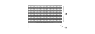
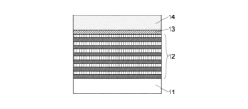
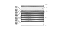
- FIG. 1 is a longitudinal sectional view showing a schematic configuration of an embodiment (first embodiment) of a first SMR type BAW filter according to the present invention
- 5 is a vertical cross-sectional view showing a substrate preparation step in the manufacturing method of the SMR type BAW filter according to the first embodiment.
- FIG. 4A to 4C are longitudinal sectional views showing intermediate steps of an acoustic Bragg reflector fabrication process in a method for manufacturing the SMR type BAW filter according to the first embodiment.
- 4A to 4C are longitudinal sectional views showing intermediate steps of an acoustic Bragg reflector fabrication process in a method for manufacturing the SMR type BAW filter according to the first embodiment.
- FIG. 4 is a longitudinal sectional view showing a state in which an acoustic Bragg reflector is fabricated in the manufacturing method of the SMR type BAW filter according to the first embodiment.
- FIG. 4 is a vertical cross-sectional view showing a state in which a first electrode layer is fabricated in a manufacturing method of the SMR type BAW filter according to the first embodiment.
- FIG. 4 is a vertical cross-sectional view showing a state in which a piezoelectric layer is fabricated in a manufacturing method of the SMR type BAW filter according to the first embodiment.
- FIG. 4 is a scanning electron microscope photograph of a vertical cross section of the SMR type BAW filter according to the first embodiment, in which the piezoelectric layer is made of zinc oxide.
- FIG. 1 is a scanning electron microscope photograph of a longitudinal section of an SMR type BAW filter according to a first embodiment, in which a piezoelectric layer is made of magnesium zinc oxide.
- 4 is a scanning electron microscope photograph of a longitudinal section of the SMR type BAW filter according to the first embodiment, in which the piezoelectric layer is made of scandium aluminum nitride.
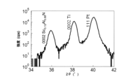
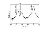
- 4 is a graph showing the results of X-ray diffraction measurement by 2 ⁇ - ⁇ scanning on the SMR type BAW filter according to the first embodiment in which the piezoelectric layer is made of zinc oxide.
- 4 is a graph showing the results of X-ray diffraction measurement by 2 ⁇ - ⁇ scan for the SMR type BAW filter according to the first embodiment, in which the piezoelectric layer is made of magnesium zinc oxide.
- 4 is a graph showing the results of X-ray diffraction measurement by 2 ⁇ - ⁇ scanning for the SMR type BAW filter according to the first embodiment in which the piezoelectric layer is made of scandium aluminum nitride.
- 3 is a (002) plane pole figure obtained by X-ray diffraction for the first acoustic impedance layer in the SMR type BAW filter of the first embodiment.
- FIG. 3 is a (10-12) plane pole figure obtained by X-ray diffraction for the second acoustic impedance layer in the SMR type BAW filter of the first embodiment.
- FIG. 3 is a (10-11) plane pole figure obtained by X-ray diffraction for a piezoelectric layer made of zinc oxide in the SMR type BAW filter of the first embodiment.
- FIG. 3 is a (10-11) plane pole figure obtained by X-ray diffraction for a piezoelectric layer made of magnesium zinc oxide in the SMR type BAW filter of the first embodiment.
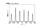
- FIG. 3 is a (10-11) plane pole figure obtained by X-ray diffraction for a piezoelectric layer made of scandium aluminum nitride in the SMR type BAW filter of the first embodiment.
- FIG. 4 is an electron diffraction image obtained for a piezoelectric layer made of zinc oxide in the SMR type BAW filter of the first embodiment.
- 4 is an electron diffraction pattern obtained for a piezoelectric layer made of scandium aluminum nitride in the SMR type BAW filter of the first embodiment.
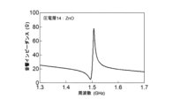
- 4 is a graph showing the results of measuring frequency characteristics of the SMR type BAW filter according to the first embodiment, in which the piezoelectric layer is made of zinc oxide.
- FIG. 4 is a graph showing the results of measuring frequency characteristics of the SMR type BAW filter according to the first embodiment, in which the piezoelectric layer is made of magnesium zinc oxide. 4 is a graph showing the results of measuring frequency characteristics of the SMR type BAW filter according to the first embodiment, in which the piezoelectric layer is made of scandium aluminum nitride.
- FIG. 4 is a vertical sectional view showing a schematic configuration of a modified example of the SMR type BAW filter of the first embodiment. 1 is a scanning electron microscope photograph of a vertical cross section of an example of an SMR type BAW filter according to a first embodiment, in which a piezoelectric layer made of scandium aluminum nitride (Sc 0.12 Al 0.88 N) is produced without heating.
- Sc 0.12 Al 0.88 N scandium aluminum nitride
- 1 is a scanning electron microscope photograph of a vertical cross section of an example of an SMR type BAW filter according to a first embodiment, in which a piezoelectric layer made of scandium aluminum nitride (Sc 0.40 Al 0.60 N) is produced without heating.
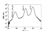
- 1 is a graph showing the results of X-ray diffraction measurement by 2 ⁇ - ⁇ scanning for an example of the SMR type BAW filter according to the first embodiment, in which a piezoelectric layer made of Sc 0.12 Al 0.88 N is fabricated without heating.
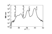
- 1 is a graph showing the results of X-ray diffraction measurement by 2 ⁇ - ⁇ scanning for an example of the SMR type BAW filter according to the first embodiment, in which a piezoelectric layer made of Sc 0.40 Al 0.60 N is fabricated without heating.
- 1 is a (10-11) plane pole figure obtained by X-ray diffraction for an example of the SMR type BAW filter according to the first embodiment, in which a piezoelectric layer made of Sc 0.12 Al 0.88 N is fabricated without heating.
- 1 is a (10-11) plane pole figure obtained by X-ray diffraction for an example of the SMR type BAW filter according to the first embodiment, in which a piezoelectric layer made of Sc 0.40 Al 0.60 N is fabricated without heating.
- FIG. 1 is an electron diffraction image of a piezoelectric layer made of Sc 0.12 Al 0.88 N, obtained for an example of the SMR type BAW filter according to the first embodiment, which is fabricated without heating the piezoelectric layer.
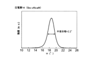
- 13 is a graph showing the results of X-ray diffraction measurement by ⁇ scan on a piezoelectric layer obtained in an example of the SMR type BAW filter according to the first embodiment, in which a piezoelectric layer made of Sc 0.12 Al 0.88 N is fabricated without heating.
- FIG. 1 is a graph showing the results of X-ray diffraction measurement performed by ⁇ scanning in the (10-11) plane on a piezoelectric layer obtained in an example of the SMR type BAW filter according to the first embodiment, in which a piezoelectric layer made of Sc 0.12 Al 0.88 N was fabricated without heating.
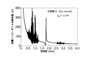
- 10 is a graph showing the results of measuring the acoustic impedance of an example of the SMR type BAW filter according to the first embodiment, in which a piezoelectric layer made of Sc 0.12 Al 0.88 N is fabricated without heating.
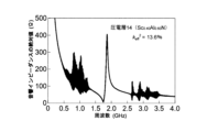
- FIG. 4 is a graph showing the results of measuring the acoustic impedance of an example of the SMR type BAW filter according to the first embodiment, in which a piezoelectric layer made of Sc 0.40 Al 0.60 N is fabricated without heating.
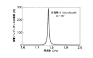
- 13 is a graph showing the results of determining the real part of the acoustic impedance of an example of the SMR type BAW filter according to the first embodiment, in which a piezoelectric layer made of Sc 0.12 Al 0.88 N is fabricated without heating.
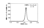
- 13 is a graph showing the results of determining the real part of the acoustic impedance of an example of the SMR type BAW filter according to the first embodiment, in which a piezoelectric layer made of Sc 0.40 Al 0.60 N is fabricated without heating.
- FIG. 11 is a longitudinal sectional view showing a schematic configuration of a second embodiment (second embodiment) of a second SMR type BAW filter according to the present invention.
- FIG. 11 is a longitudinal sectional view showing a schematic configuration of a multiple integrated device in which two or more SMR type BAW filters according to a second embodiment are combined.
- 10A to 10C are vertical cross-sectional views showing a manufacturing process of a multiple integrated device.
- 10A to 10C are vertical cross-sectional views showing a manufacturing process of a multiple integrated device.
- 10A to 10C are vertical cross-sectional views showing a manufacturing process of a multiple integrated device.
- 10A to 10C are vertical cross-sectional views showing a manufacturing process of a multiple integrated device.
- 10A to 10C are vertical cross-sectional views showing a manufacturing process of a multiple integrated device.
- 13 is a scanning electron microscope photograph of a longitudinal section of an SMR type BAW filter according to a second embodiment, in which the piezoelectric layer is made of zinc oxide.
- 13 is a scanning electron microscope photograph of a longitudinal section of an SMR type BAW filter according to a second embodiment, in which a piezoelectric layer is made of magnesium zinc oxide.
- 13 is a scanning electron microscope photograph of a longitudinal section of an SMR type BAW filter according to a second embodiment, in which a piezoelectric layer is made of scandium aluminum nitride.
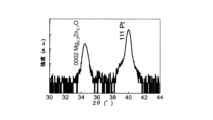
- 13 is a graph showing the results of X-ray diffraction measurement by 2 ⁇ - ⁇ scanning on the SMR type BAW filter according to the second embodiment, in which the piezoelectric layer is made of zinc oxide.
- 13 is a graph showing the results of X-ray diffraction measurement by 2 ⁇ - ⁇ scanning on the SMR type BAW filter according to the second embodiment, in which the piezoelectric layer is made of magnesium zinc oxide.
- 13 is a graph showing the results of X-ray diffraction measurement by 2 ⁇ - ⁇ scanning on the SMR type BAW filter according to the second embodiment, in which the piezoelectric layer is made of scandium aluminum nitride.
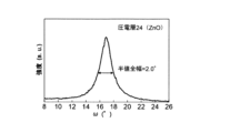
- 13 is a graph showing the results of X-ray diffraction measurement by ⁇ scan for an SMR type BAW filter according to a second embodiment in which the piezoelectric layer is made of zinc oxide.
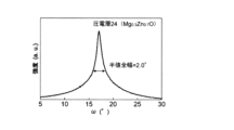
- 13 is a graph showing the results of X-ray diffraction measurement by ⁇ scan for an SMR type BAW filter according to a second embodiment in which the piezoelectric layer is made of magnesium zinc oxide.
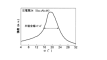
- 13 is a graph showing the results of X-ray diffraction measurement by ⁇ scan for the SMR type BAW filter according to the second embodiment, in which the piezoelectric layer is made of scandium aluminum nitride.
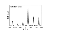
- 13 is a graph showing the results of X-ray diffraction measurement performed by ⁇ scanning in the (10-11) plane on the SMR type BAW filter according to the second embodiment, in which the piezoelectric layer is made of zinc oxide.
- 13 is a graph showing the results of X-ray diffraction measurement performed by ⁇ scanning in the (10-11) plane for the SMR type BAW filter according to the second embodiment, in which the piezoelectric layer is made of magnesium zinc oxide.
- 13 is a graph showing the results of X-ray diffraction measurement performed by ⁇ scanning in the (10-11) plane on the SMR type BAW filter according to the second embodiment, in which the piezoelectric layer is made of scandium aluminum nitride.
- 11 is a pole figure of the (10-11) plane of the piezoelectric layer obtained by X-ray diffraction for the SMR type BAW filter according to the second embodiment, in which the piezoelectric layer is made of zinc oxide.
- 11 is a pole figure of the (10-11) plane of the piezoelectric layer obtained by X-ray diffraction for the SMR type BAW filter according to the second embodiment, in which the piezoelectric layer is made of magnesium zinc oxide.
- 11 is a (10-11) plane pole figure of a piezoelectric layer obtained by X-ray diffraction for an SMR type BAW filter according to a second embodiment in which the piezoelectric layer is made of scandium aluminum nitride.
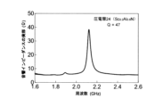
- 13 is a graph showing the results of measuring the acoustic impedance of the SMR type BAW filter according to the second embodiment, in which the piezoelectric layer is made of scandium aluminum nitride.
- 13 is a graph showing the results of determining the real part of the acoustic impedance of the SMR type BAW filter according to the second embodiment, in which the piezoelectric layer is made of scandium aluminum nitride.
- FIG. 1 is a longitudinal sectional view showing a schematic configuration of an SMR BAW filter 10, which is an embodiment (first embodiment) of the first SMR BAW filter.
- the SMR BAW filter 10 has a structure in which a substrate 11, an acoustic Bragg reflector 12, a first electrode layer 13, a piezoelectric layer 14, and a second electrode layer 15 are laminated in this order.
- the substrate 11 is used for manufacturing the SMR BAW filter 10, and is not essential as a component of the SMR BAW filter 10, so it is not necessary to provide it. However, since the substrate 11 does not affect the operation of the SMR BAW filter 10 and has a secondary role of holding the SMR BAW filter 10, it is left as it is in this embodiment.
- the substrate 11 is made of single crystal sapphire having a hexagonal crystal structure. This single crystal sapphire is cut so that the (0001) plane of the crystal appears on the surface of the substrate 11.
- single crystals such as silicon carbide (SiC), silicon (Si), magnesium oxide (MgO), strontium titanate (SrTiO 3 ), gallium arsenide (GaAs), and germanium (Ge) may be used as the material for the substrate 11.
- the acoustic Bragg reflector 12 has a structure in which first acoustic impedance layers 121 and second acoustic impedance layers 122 made of different materials are alternately stacked one by one.
- first acoustic impedance layers 121 and second acoustic impedance layers 122 are provided, but this number of layers is not limited and it is sufficient that there are at least two of each.
- Both the first acoustic impedance layer 121 and the second acoustic impedance layer 122 are made of metal.
- both the first acoustic impedance layer 121 and the second acoustic impedance layer 122 are fabricated by an epitaxial method as described below, and are therefore oriented polycrystalline or single crystalline.
- the first acoustic impedance layer 121 is made of platinum (Pt), and the second acoustic impedance layer 122 is made of titanium (Ti). Since titanium is made of lighter atoms than platinum, the second acoustic impedance layer 122 has a lower acoustic impedance than the first acoustic impedance layer 121. Specifically, the acoustic impedance of the first acoustic impedance layer 121 is 85 ⁇ 10 6 , and the acoustic impedance of the second acoustic impedance layer 122 is 27 ⁇ 10 6 , resulting in a high acoustic impedance ratio index value of 3.15.
- acoustic Bragg reflection can be realized by providing six layers each of the first acoustic impedance layer 121 and the second acoustic impedance layer 122.
- platinum and titanium have similar thermal expansion coefficients (the linear expansion coefficient at room temperature for platinum is 8.8 ⁇ 10-6 /K and for titanium is 8.4 ⁇ 10-6 /K), and as a result, the thermal expansion coefficients of the first acoustic impedance layer 121 and the second acoustic impedance layer 122 are also similar (thermal expansion coefficient ratio index value is 1.05), thereby reducing the risk of one of the first acoustic impedance layer 121 and the second acoustic impedance layer 122 peeling off from the other due to expansion or contraction caused by temperature changes.
- the materials of the first acoustic impedance layer 121 and the second acoustic impedance layer 122 are not limited to the above examples.
- the material of the first acoustic impedance layer 121 can be, in addition to platinum, for example, molybdenum (Mo), tantalum (Ta), hafnium (Hf), iridium (Ir), ruthenium (Ru), tungsten (W), gold (Au), zirconium (Zr), niobium (Nb), or other simple substances or alloys thereof.
- the material of the second acoustic impedance layer 122 can be, in addition to titanium, for example, scandium (Sc), vanadium (V), chromium (Cr), manganese (Mn), iron (Fe), cobalt (Co), nickel (Ni), copper (Cu), zinc (Zn), germanium (Ge), aluminum (Al), silicon (Si), carbon (C), or other simple substances or alloys thereof.
- simple carbon (C) graphene having metallic thermal conductivity is used.
- the atoms of the elements listed here that are the materials of the second acoustic impedance layer 122 are all lighter than the atoms of the elements that are the materials of the
- the first electrode layer 13 is not particularly limited as long as it is a layer made of a conductive material, but in this embodiment, as described below, it is produced by an epitaxial method, and is therefore an oriented polycrystal or single crystal.
- the material of the electrode is platinum. Note that if the acoustic Bragg reflector 12 has a sufficiently high conductivity as an electrode, the first electrode layer 13 may be omitted and the acoustic Bragg reflector 12 may be used as an electrode.
- the piezoelectric layer 14 is made of a polycrystalline or single-crystalline piezoelectric material oriented in a predetermined direction.
- three types of SMR-type BAW filters 10 were fabricated in which the piezoelectric layer 14 is made of single crystals of zinc oxide (ZnO), magnesium zinc oxide (MgZnO), and scandium aluminum nitride (ScAlN). All three types of materials have a hexagonal wurtzite structure.
- all three types of piezoelectric layers 14 are fabricated by the epitaxial method, as described below, and the c-axis is oriented in a direction perpendicular to the piezoelectric layer 14.
- the top and bottom surfaces of the piezoelectric layer 14 have hexagonal (0001) crystal faces, and the atoms are arranged on the surfaces to have six-fold rotational symmetry around the c-axis.
- the material of the piezoelectric layer 14 is not limited to these three examples, and other piezoelectric materials such as aluminum nitride (AlN) may be used.
- the second electrode layer 15 is not particularly limited as long as it is a layer made of a conductive material. In this embodiment, the second electrode layer 15 made of gold is used. The second electrode layer 15 does not need to be an oriented polycrystalline or single crystalline material, and does not need to be produced by an epitaxial method.
- the SMR type BAW filter 10 of this embodiment is manufactured by the method shown in Figures 2A to 2F.
- a substrate 11 made of single crystal sapphire cut so that the (0001) plane of the crystal appears on the surface is prepared ( Figure 2A: substrate preparation step).
- Such substrates are commercially available, so such commercially available ones may be used as the substrate 11 as they are.
- the acoustic Bragg reflector 12 (FIGS. 2B to 2D: acoustic Bragg reflector fabrication process), the first electrode layer 13 (FIG. 2E), and the piezoelectric layer 14 (FIG. 2F) were fabricated on the substrate 11 in this order by epitaxial growth (FIGS. 2B to 2F).
- an RF (radio frequency) magnetron sputtering device was used to fabricate each of these layers.
- a layer of the first acoustic impedance layer 121 was fabricated on the substrate 11 (FIG.
- a layer of the second acoustic impedance layer 122 was fabricated on the fabricated first acoustic impedance layer 121 (FIG. 2C), and the first acoustic impedance layer 121 was fabricated on the fabricated second acoustic impedance layer 122. These operations were repeated.
- the conditions for the RF magnetron sputtering device used in forming each layer are as follows: (First acoustic impedance layer 121) A platinum target was placed on the cathode of an RF magnetron sputtering device, and the surface of the substrate 11 or the second acoustic impedance layer 122 on which the first acoustic impedance layer 121 was to be formed was placed at a position 30 mm away from the target. Films were formed in an argon gas atmosphere at a pressure of 0.5 Pa, at a temperature of 500° C., for 10 minutes per layer, until the thickness reached 450 nm.
- (Second acoustic impedance layer 122) A titanium target was placed on the cathode of an RF magnetron sputtering device, and the surface of the first acoustic impedance layer 121 on which the second acoustic impedance layer 122 was to be formed was placed at a position 30 mm away from the target, facing the target. Films were formed in an argon gas atmosphere at a pressure of 0.5 Pa, at a temperature of 350° C., for 30 minutes per layer, until the thickness reached 760 nm.
- First electrode layer 13 A platinum target was placed on the cathode of an RF magnetron sputtering device, and the surface of the second acoustic impedance layer 122 on which the first electrode layer 13 was to be formed was placed at a position 30 mm away from the target so as to face the target. A film was formed at a temperature of 500° C. for 2 minutes in an argon gas atmosphere at a pressure of 0.5 Pa while applying a high frequency power of 80 W until the film reached a thickness of 150 nm.
- piezoelectric layer 14 When the piezoelectric layer 14 was made of zinc oxide, a zinc oxide target was placed on the cathode of an RF magnetron sputtering device, and the surface of the first electrode layer 13 was placed at a position 30 mm away from the target so as to face it. A film was formed to a thickness of 1.2 ⁇ m at a temperature of 500° C. for 30 minutes in an atmosphere of a mixed gas of argon and oxygen (partial pressure ratio of argon:oxygen:3:1) at a pressure of 1 Pa while supplying a high frequency power of 150 W.
- a mixed gas of argon and oxygen partial pressure ratio of argon:oxygen:3:1
- the piezoelectric layer 14 was made of magnesium zinc oxide
- a target made of magnesium zinc oxide was used, and the film was deposited under the same arrangement conditions as for zinc oxide, in an atmosphere of a mixed gas of argon and oxygen (partial pressure ratio is the same as above) at a pressure of 1 Pa, at a temperature of 450°C for 40 minutes, while supplying 80 W of high frequency power, until the film reached a thickness of 1.0 ⁇ m.
- the piezoelectric layer 14 was made of scandium aluminum nitride
- a target made of scandium aluminum nitride was used, and the film was deposited under the same arrangement conditions as in the case of zinc oxide, in an atmosphere of a mixed gas of argon and nitrogen (partial pressure ratio of 4 parts argon to 1 part nitrogen) at a pressure of 0.5 Pa, at a temperature of 450°C for 60 minutes, until the film reached a thickness of 2.1 ⁇ m.
- the acoustic Bragg reflector 12, the first electrode layer 13, and the piezoelectric layer 14 are all fabricated by the epitaxial method, so that each layer of the acoustic Bragg reflector 12 and the first electrode layer 13 are formed as polycrystals or single crystals oriented to match the crystal lattice of the single crystal of the substrate 11, and the piezoelectric layer 14 is formed as polycrystals or single crystals oriented to match the crystal lattice of each layer of the acoustic Bragg reflector 12 and the first electrode layer 13.
- the second electrode layer 15 is fabricated on the piezoelectric layer 14, completing the SMR type BAW filter 10.
- the second electrode layer 15 does not need to be fabricated by the epitaxial method, but can be fabricated using a normal deposition method, etc.
- Figures 3A to 3C show scanning electron microscope (SEM) photographs of the vertical cross section of the manufactured SMR type BAW filter 10. No columnar structure is observed in the piezoelectric layer 14 whether the piezoelectric layer 14 is made of zinc oxide (Figure 3A), zinc magnesium oxide (Figure 3B), or scandium aluminum nitride ( Figure 3C).
- the piezoelectric layer 14 is made of any of zinc oxide (FIG. 4A), magnesium zinc oxide (FIG. 4B), and scandium aluminum nitride (FIG. 4C)
- the diffraction peaks of the (0002) plane of the crystals were observed.
- the diffraction peaks of the (0002) plane of the hexagonal Ti crystal and the (111) plane of the Pt crystal having a face-centered cubic structure (cubic crystal) were also observed.
- the (111) plane of the face-centered cubic crystal has six-fold rotational symmetry like the (0002) plane of the hexagonal crystal.
- the piezoelectric layer 14 was fabricated in a heated state, but the following will show an example in which the piezoelectric layer 14 is made of scandium aluminum nitride and is fabricated without heating with a heater.
- the atomic ratio of scandium to aluminum was (i) 12:88 ( Sc0.12Al0.88N ) as above, and (ii) 4:6 ( Sc0.40Al0.60N ) with a higher ratio of scandium than that.
- a buffer layer 141 made of Sc0.12Al0.88N was fabricated on the first electrode layer 13, and a piezoelectric layer 14 made of Sc0.40Al0.60N was fabricated thereon.
- the fabrication conditions for the piezoelectric layer 14 other than the temperature were a gas atmosphere of a mixed gas of argon and nitrogen at a pressure of 0.5 Pa, a high frequency power of 100 W was applied , and the film was grown to a thickness of 1.6 ⁇ m.
- the fabrication conditions other than the piezoelectric layer 14 were the same as those in the above example, except that the number of layers in each of the first acoustic impedance layer 121 and the second acoustic impedance layer 122 of the acoustic Bragg reflector 12 was set to 5. Separately, an attempt was made to fabricate the piezoelectric layer 14 by heating the structure of (ii) to 450° C., but in that case, it was not possible to obtain an epitaxially grown piezoelectric layer 14.
- a SEM photograph of the longitudinal section is shown in Fig. 9A
- the results of X-ray diffraction measurement by 2 ⁇ - ⁇ scanning are shown in Fig. 10A
- a pole figure of the (10-11) plane of the piezoelectric layer 14 obtained by X-ray diffraction is shown in Fig. 11A
- the results of measuring the acoustic impedance are shown in Fig. 15A
- the results of calculating the real part of the acoustic impedance are shown in Fig. 16A.
- a SEM photograph of the longitudinal section is shown in Fig. 9B
- the results of 2 ⁇ - ⁇ scanning are shown in Fig. 10B
- a pole figure of the (10-11) plane of the piezoelectric layer 14 is shown in Fig. 11B
- the results of measuring the acoustic impedance are shown in Fig. 15B
- the results of calculating the real part of the acoustic impedance are shown in Fig. 16B.
- the piezoelectric layer 14 is Sc0.12Al0.88N
- an electron diffraction image is shown in FIG. 12
- the result of X-ray diffraction measurement by ⁇ scan is shown in FIG. 13
- the result of X-ray diffraction measurement by ⁇ scan in the (10-11) plane is shown in FIG. 14.
- the X-ray diffraction peak in the 2 ⁇ - ⁇ scan is one order of magnitude larger than that in the case of the piezoelectric layer 14 made of the same composition while heating it to 450°C (FIG. 10A vs. FIG. 4C), a spot with a clearer six-fold rotational symmetry is observed in the (10-11) plane pole figure (FIG. 11A vs. FIG. 5E), and a clearer electron diffraction image is obtained (FIG. 12 vs. FIG. 6B).
- the piezoelectric layer 14 made of Sc 0.40 Al 0.60 N was prepared without heating, as shown particularly in the (10-11) plane pole figure in Fig. 11B, it is shown that the piezoelectric layer 14 is oriented while inheriting the six-fold rotational symmetry in the crystals of the substrate 11 and the acoustic Bragg reflector 12. Such an orientation cannot be obtained when the piezoelectric layer 14 made of Sc 0.40 Al 0.60 N is prepared while heating.
- keff2 which is the square of the effective value keff of the electromechanical coupling constant, was calculated based on the results, resulting in 5.1% for the example in which the piezoelectric layer 14 was made of Sc0.12Al0.88N and 13.6% for the example in which the piezoelectric layer 14 was made of Sc0.40Al0.60N .
- This result shows that as the content of Sc, which has a larger atomic weight than Al, increases, keff2 increases and the acoustic characteristics improve.
- the Q value estimated from the real part of the acoustic impedance was 167 in an example in which the piezoelectric layer 14 was made of Sc 0.12 Al 0.88 N, and 38 in an example in which the piezoelectric layer 14 was made of Sc 0.40 Al 0.60 N.
- This result indicates that as the Sc content increases, the ratio c/a of the c-axis length to the a-axis length decreases, which in turn increases keff 2 , thereby improving the piezoelectric characteristics.
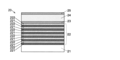
- FIG. 17 shows the configuration of an SMR BAW filter 20, which is an embodiment (second embodiment) of the second SMR BAW filter.
- the SMR BAW filter 20 has a structure in which a substrate 21, an acoustic Bragg reflector 22, a first electrode layer 23, a piezoelectric layer 24, and a second electrode layer 25 are laminated in this order.
- the substrate 21, the first electrode layer 23, the piezoelectric layer 24, and the second electrode layer 25 are similar to the substrate 11, the first electrode layer 13, the piezoelectric layer 14, and the second electrode layer 15 in the SMR BAW filter 10 of the first embodiment, respectively.
- the acoustic Bragg reflector 22 has a structure in which a first acoustic impedance layer 221 made of metal and a second acoustic impedance layer 222 made of ceramics are alternately stacked one by one.
- the first acoustic impedance layer 221 and the second acoustic impedance layer 222 are provided in six layers, but this number of layers is not limited and it is sufficient that there are two or more layers of each.
- Both the first acoustic impedance layer 221 and the second acoustic impedance layer 222 are oriented polycrystals or single crystals produced by the epitaxial method.
- Metals used as materials for the first acoustic impedance layer 221 include, for example, platinum or titanium. Ceramics used as materials for the second acoustic impedance layer 222 include zinc oxide, magnesium zinc oxide, aluminum nitride, and scandium aluminum nitride. The combination of the materials for the first acoustic impedance layer 221 and the second acoustic impedance layer 222 is selected so that the acoustic impedances of the two layers are different from each other.
- the method for manufacturing the SMR BAW filter 20 of the second embodiment is similar to the method for manufacturing the SMR BAW filter 10 of the first embodiment, except that ceramics are epitaxially grown (instead of metal in the first embodiment) when producing the second acoustic impedance layer 222.
- the method for epitaxially growing the ceramics of the second acoustic impedance layer 222 is similar to the method for epitaxially growing the ceramics of the piezoelectric layers 14 and 24.
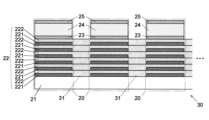
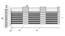
- the SMR type BAW filter of the second embodiment can be, for example, as shown in FIG. 18, combined into an integrated device (hereinafter, simply referred to as a "device") 30 by combining two or more of them.
- a device an integrated device (hereinafter, simply referred to as a "device") 30 by combining two or more of them.
- an acoustic Bragg reflector 22, a first electrode layer 23, a piezoelectric layer 24, and a second electrode layer 25, each of which is formed in this order from the bottom, are formed at different positions on a single substrate 21.
- a connecting material 31 made of the same ceramic as the second acoustic impedance layer 222 is provided between the acoustic Bragg reflectors 22.
- the second acoustic impedance layer 222 and the connecting material 31 are integrally formed.
- the individual SMR type BAW filters 20 may be arranged in a one-dimensional array or in a two-dimensional array.
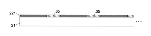
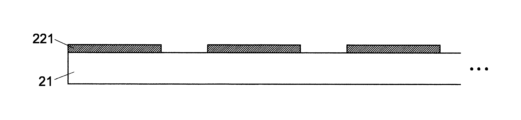
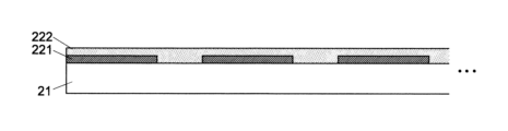
- the device 30 can be manufactured by the following method. First, a mask 35 is formed at the position on the substrate 21 where the connecting material 31 is to be provided, and then a first acoustic impedance layer 221 made of metal is formed on the substrate 21 by epitaxial growth (FIG. 19A). Next, the mask 35 is removed (FIG. 19B), and a second acoustic impedance layer 222 made of ceramics and the connecting material 31 are simultaneously formed by epitaxial growth (FIG. 19C). The above operations are repeated to form an acoustic Bragg reflector 22.
- a mask 35 is formed on the upper surface of the connecting material 31, and then a first electrode layer 23 and a piezoelectric layer 24 are formed on the acoustic Bragg reflector 22 in this order by epitaxial growth (FIG. 19D). Finally, a second electrode layer 25 is formed on the piezoelectric layer 24 (either by epitaxial growth or by another method), thereby completing the device 30. With this method, the second acoustic impedance layer 222 and the connecting material 31 are formed simultaneously, simplifying the manufacturing process.
- the fabricated SMR BAW filters 20 all had a first acoustic impedance layer 221 made of metal platinum, a second acoustic impedance layer 222 made of ceramic zinc oxide, and three types of piezoelectric layers 24 made of zinc oxide (ZnO), magnesium zinc oxide (Mg0.3Zn0.7O ) , or scandium aluminum nitride ( Sc0.2Al0.8N ).
- the piezoelectric layer 24 is made of ZnO has the suffix "A" (e.g., Figure 20A)
- the one in which the piezoelectric layer 24 is made of Mg 0.3 Zn 0.7 O has the suffix "B" (e.g., Figure 20B)
- the one in which the piezoelectric layer 24 is made of Sc 0.2 Al 0.8 N has the suffix "C” (e.g., Figure 20C).
- the piezoelectric layer 24 had the desired crystals (ZnO, Mg0.3Zn0.7O , Sc0.2Al0.8N ) formed (Figs.
- the piezoelectric layers 24 made of ZnO and Mg0.3Zn0.7O each had smaller full width at half maximum profiles obtained by ⁇ scan (Figs. 22A to 22C ) and better crystallinity than the piezoelectric layer 24 made of Sc0.2Al0.8N .
- An SMR type BAW filter comprises: a) an acoustic Bragg reflector in which a first acoustic impedance layer and a second acoustic impedance layer, each of which is made of a polycrystal or single crystal of a metal oriented in a predetermined direction and has a different acoustic impedance from each other, are alternately laminated in a plurality of layers, b) a piezoelectric layer provided on the acoustic Bragg reflector and made of a polycrystalline or single crystalline piezoelectric material oriented in a predetermined direction, wherein the crystal lattice of the polycrystalline or single crystalline material matches the polycrystalline or single crystalline crystal lattice of a metal of one of the first acoustic impedance layer and the second acoustic impedance layer which is located closest to the piezoelectric layer.
- the SMR type BAW filter according to 2 is an SMR type BAW filter according to 1, in which the thermal expansion coefficient ratio index value, which is the value obtained by dividing the higher of the thermal expansion coefficient value of the first acoustic impedance layer and the thermal expansion coefficient value of the second acoustic impedance layer by the lower, is within the range of 1.0 to 1.1.
- the SMR type BAW filter according to clause 3 is an SMR type BAW filter according to clause 1 or 2, in which the acoustic impedance ratio index value, which is the value obtained by dividing the higher of the acoustic impedance value of the first acoustic impedance layer and the acoustic impedance value of the second acoustic impedance layer by the lower, is 3 or more.
- the SMR type BAW filter according to 4 is the SMR type BAW filter according to 2 or 3, in which one of the first acoustic impedance layer and the second acoustic impedance layer is made of platinum and the other is made of titanium.
- Another aspect of the present invention provides an SMR type BAW filter, a) an acoustic Bragg reflector in which a first acoustic impedance layer made of a metal polycrystal or single crystal oriented in a predetermined direction and a second acoustic impedance layer made of a ceramic polycrystal or single crystal oriented in a predetermined direction and having an acoustic impedance different from that of the first acoustic impedance layer are alternately laminated one by one; b) a piezoelectric layer provided on the acoustic Bragg reflector and made of a polycrystalline or single crystalline piezoelectric material oriented in a predetermined direction, wherein the crystal lattice of the polycrystalline or single crystalline material matches the crystal lattice of the polycrystalline or single crystalline material of one of the first acoustic impedance layer and the second acoustic impedance layer which is located closest to the piezoelectric layer.
- the SMR type BAW filter according to the 6th paragraph is Two SMR type BAW filters according to claim 5 are arranged in a direction parallel to the first acoustic impedance layer and the second acoustic impedance layer, and are spaced apart from each other; The acoustic Bragg reflectors in the two SMR type BAW filters are connected to each other by the connecting material made of ceramics.
- a method for manufacturing an SMR type BAW filter comprises the steps of: a substrate preparation step of preparing a substrate made of a single crystal having a predetermined crystal plane on its surface; an acoustic Bragg reflector fabrication process for fabricating an acoustic Bragg reflector by forming, on a surface of the substrate, a first acoustic impedance layer and a second acoustic impedance layer, each of which is made of a metal having a crystal lattice matching with the crystal lattice of the single crystal of the substrate and has a different acoustic impedance, alternately in a single layer and a plurality of layers by an epitaxial method; and a piezoelectric layer fabrication step of fabricating, on the acoustic Bragg reflector, a piezoelectric layer made of a piezoelectric material having a crystal lattice that matches the crystal lattice of the metal of the uppermost layer of the first
- a method for manufacturing an SMR type BAW filter according to item 8 includes the steps of: a substrate preparation step of preparing a substrate made of a single crystal having a predetermined crystal plane on its surface; an acoustic Bragg reflector fabrication process for fabricating an acoustic Bragg reflector by forming, on the surface of the substrate, a first acoustic impedance layer made of a metal polycrystal or single crystal oriented in a predetermined direction and a second acoustic impedance layer made of a ceramic polycrystal or single crystal oriented in a predetermined direction and having an acoustic impedance different from that of the first acoustic impedance layer, one layer at a time, in multiple layers by an epitaxial method; and a piezoelectric layer fabrication step of fabricating, on the acoustic Bragg reflector, a piezoelectric layer made of a piezoelectric material having a crystal lattice that matches the crystal lattic
- the method for producing an SMR type BAW filter according to item 9 further comprises the steps of: When preparing the first acoustic impedance layer and the second acoustic impedance layer, two of each layer are prepared so as to be spaced apart from each other in a direction parallel to the first acoustic impedance layer and the second acoustic impedance layer, At the same time as producing the second acoustic impedance layer, polycrystals or single crystals of the ceramics are epitaxially grown between the two second acoustic impedance layers and between the two first acoustic impedance layers directly below the two second acoustic impedance layers.
- the SMR type BAW filter according to the first paragraph and the SMR type BAW filter according to the fifth paragraph each have the following characteristics: a) an acoustic Bragg reflector in which a first acoustic impedance layer made of a metal polycrystal or single crystal oriented in a predetermined direction and a second acoustic impedance layer made of a metal or ceramic polycrystal or single crystal oriented in a predetermined direction and having an acoustic impedance different from that of the first acoustic impedance layer are alternately laminated one by one; b) a piezoelectric layer provided on the acoustic Bragg reflector and made of a polycrystalline or single crystalline piezoelectric material oriented in a predetermined direction, wherein the crystal lattice of the polycrystalline or single crystalline material matches the crystal lattice of the polycrystalline or single crystalline material of one of the first acoustic impedance layer and the second acoustic impedance layer
- the manufacturing method of the SMR type BAW filter according to the seventh aspect and the manufacturing method of the SMR type BAW filter according to the eighth aspect are both a substrate preparation step of preparing a substrate made of a single crystal having a predetermined crystal plane on its surface; an acoustic Bragg reflector fabrication process for fabricating an acoustic Bragg reflector by forming, on the surface of the substrate, a first acoustic impedance layer made of a metal polycrystal or single crystal oriented in a predetermined direction, and a second acoustic impedance layer made of a metal or ceramic polycrystal or single crystal oriented in a predetermined direction and having an acoustic impedance different from that of the first acoustic impedance layer, one layer at a time, in multiple layers by an epitaxial method; and a piezoelectric layer fabrication step of fabricating, on the acoustic Bragg reflector, a piezoelectric layer made of a piezoelectric material having
- Reference Signs List 10 20: SMR type BAW filter 11, 21: Substrate 12, 22: Acoustic Bragg reflector 121, 221: First acoustic impedance layer 122, 222: Second acoustic impedance layer 13, 23: First electrode layer 14, 24: Piezoelectric layer 141: Buffer layer 15, 25: Second electrode layer 30: Integrated device combining two or more SMR type BAW filters 31: Connection material 35: Mask
Landscapes
- Physics & Mathematics (AREA)
- Acoustics & Sound (AREA)
- Engineering & Computer Science (AREA)
- Manufacturing & Machinery (AREA)
- Piezo-Electric Or Mechanical Vibrators, Or Delay Or Filter Circuits (AREA)
Abstract
いずれも所定の方向に配向した金属の多結晶又は単結晶から成り、互いに音響インピーダンスが異なる第1音響インピーダンス層(121)と第2音響インピーダンス層(122)が交互に1層ずつそれぞれ複数積層した音響ブラッグ反射器(12)と、音響ブラッグ反射器(12)上に設けられた、所定の方向に配向した多結晶又は単結晶の圧電体から成る圧電層(14)であって、前記多結晶又は前記単結晶の結晶格子が、前記第1音響インピーダンス層及び前記第2音響インピーダンス層のうち前記圧電層に近い位置にある層の金属の多結晶又は単結晶の結晶格子と整合している圧電層(14)とを備える。
Description
本発明は、スマートフォン等の通信機器等で使用される周波数フィルタであるバルク音響波(BAW:Bulk Acoustic Wave)フィルタ、特にソリッドマウント共振器(SMR:Solidly Mounted Resonator)型のBAWフィルタ及びその製造方法に関する。
BAWフィルタは、圧電体から成る層である圧電層のバルクの振動を利用して特定の周波数帯の電気信号を通過させる周波数フィルタである。圧電層を用いた周波数フィルタとしては、圧電層の表面に生じる表面弾性波(SAW:Surface Acoustic Wave)を利用したSAWフィルタも用いられているが、BAWフィルタはSAWフィルタよりも耐電圧性が高く、且つ、より高い周波数帯で使用することができるという特徴を有する。
BAWフィルタには、SMR型のものとFBAR(Film Bulk Acoustic Resonator)型のものが存在する。SMR型のBAWフィルタは、音響インピーダンスが異なる層が交互に積層して成る音響ブラッグ反射器の上に圧電層を備える。これに対して、FBAR型のBAWフィルタは、一部に空洞が設けられた基板の該空洞上を含む上面に圧電層を備える。このような構造の相違により、SMR型のBAWフィルタはFBAR型のものよりも機械的強度が高いという特徴を有する。
現状では、スマートフォン用の周波数フィルタとして実用化されているSMR型のBAWフィルタは、二酸化ケイ素(SiO2)から成る低インピーダンス層と該低インピーダンス層の構成元素よりも重い原子であるタングステン(W)やモリブデン(Mo)等の金属から成る高インピーダンス層を交互に積層した音響ブラッグ反射器と、所定の結晶軸が層に垂直な方向に配向した多数の微結晶から成る圧電体製の圧電層とを備えるものが一般的である。今後、さらに高い周波数帯に対応するためには、配向の精度が高い多結晶、又は単結晶から成る圧電体を用いた圧電層を備える周波数フィルタが求められている。
特許文献1には、シリコン(Si)、酸化マグネシウム(MgO)、チタン酸ストロンチウム(SrTiO3)等の単結晶から成る基板の表面に、ジルコニウム酸バリウム(BaZrO3)、マグネシウムタンタル酸バリウム(Ba(Mg1/3Ta2/3)O3)、チタン酸カルシウム(CaTiO3)等のペロブスカイト型酸化物のうちの互いに音響インピーダンスが異なる2種類をエピタキシャル法により交互に積層することで音響ブラッグ反射器を形成し、該音響ブラッグ反射器の表面にエピタキシャル法によりチタン酸バリウムから成る圧電層を形成してSMR型BAWフィルタを作製することが記載されている。このように、エピタキシャル法を用いて、基板、音響ブラッグ反射器及び圧電層と順次形成することにより、該圧電層は基板の結晶の結晶格子と整合した配向の精度が高い多結晶又は単結晶となる。そのため、高い周波数帯に対応したSMR型BAWフィルタが得られる。
圧電層では、振動のエネルギーの一部は熱に変換されるため、SMR型BAWフィルタでは、その温度上昇を防ぐために、圧電層で生じた熱をフィルタ外へ逃がす必要がある。SMR型BAWフィルタでは、入力された電気信号に従って圧電層をできるだけ外部に束縛されない状態で振動させるように音響ブラッグ反射器側が外部に固定されるため、圧電層で生じた熱は音響ブラッグ反射器を介して外部に放熱される。しかし、特許文献1に記載のSMR型BAWフィルタは、音響ブラッグ反射器を構成する高インピーダンス層及び低インピーダンス層がいずれもセラミクス(セラミックス)製であることから、伝熱性が低く、圧電層から外部への放熱性が低いという欠点を有する。
本発明が解決しようとする課題は、高い周波数帯に対応しつつ、圧電層から外部への放熱性が高いSMR型BAWフィルタを提供することである。
上記課題を解決するために成された本発明に係る第1のSMR型BAWフィルタは、
a) いずれも所定の方向に配向した金属の多結晶又は単結晶から成り、互いに音響インピーダンスが異なる第1音響インピーダンス層と第2音響インピーダンス層が交互に1層ずつそれぞれ複数積層した音響ブラッグ反射器と、
b) 前記音響ブラッグ反射器上に設けられた、所定の方向に配向した多結晶又は単結晶の圧電体から成る圧電層であって、該多結晶又は単結晶の結晶格子が、前記第1音響インピーダンス層及び前記第2音響インピーダンス層のうち該圧電層に近い位置にある層の金属の多結晶又は単結晶の結晶格子と整合している圧電層と
を備える。
a) いずれも所定の方向に配向した金属の多結晶又は単結晶から成り、互いに音響インピーダンスが異なる第1音響インピーダンス層と第2音響インピーダンス層が交互に1層ずつそれぞれ複数積層した音響ブラッグ反射器と、
b) 前記音響ブラッグ反射器上に設けられた、所定の方向に配向した多結晶又は単結晶の圧電体から成る圧電層であって、該多結晶又は単結晶の結晶格子が、前記第1音響インピーダンス層及び前記第2音響インピーダンス層のうち該圧電層に近い位置にある層の金属の多結晶又は単結晶の結晶格子と整合している圧電層と
を備える。
一般に、金属はセラミクスよりも熱伝導率が高い。本発明に係る第1のSMR型BAWフィルタにおける音響ブラッグ反射器はそれを構成する各層がいずれも金属から成るため、各層がいずれもセラミクス製の音響ブラッグ反射器よりも伝熱性が高い。そのため、本発明に係るSMR型BAWフィルタは、圧電層から音響ブラッグ反射器を介して外部へ放熱する性能を高くすることができる。
また、本発明に係る第1のSMR型BAWフィルタは、圧電層が所定の方向に配向した圧電体の多結晶又は単結晶から成るため、高い周波数帯に対応することができる。
このような構成を有するSMR型BAWフィルタは、音響ブラッグ反射器の各層と圧電層を順にエピタキシャル法で作製することにより、容易に製造することができる。すなわち、このような構成を有するSMR型BAWフィルタを製造する方法は、
所定の結晶面を表面に有する単結晶から成る基板を準備する基板準備工程と、
前記基板の表面に、いずれも前記基板の単結晶の結晶格子と整合する結晶格子を有する金属から成り、互いに音響インピーダンスが異なる第1音響インピーダンス層と第2音響インピーダンス層を交互に1層ずつそれぞれ複数、エピタキシャル法で形成することにより音響ブラッグ反射器を作製する音響ブラッグ反射器作製工程と、
前記音響ブラッグ反射器の上に、前記第1音響インピーダンス層と前記第2音響インピーダンス層のうち最上部にある層の金属の結晶格子と整合する結晶格子を有する圧電体から成る圧電層をエピタキシャル法により作製する圧電層作製工程と
を有する。
前記基板における前記所定の結晶面は、圧電層に形成する多結晶の配向方向又は単結晶の結晶軸の方向に応じて定める。例えば、六方晶の結晶構造を有する酸化亜鉛(ZnO)、酸化マグネシウム亜鉛(MgZnO)、窒化アルミニウム(AlN)、窒化スカンジウムアルミニウム(ScAlN)等から成る圧電層を、(0001)面が圧電層に平行になるように作製する場合には、基板には3回回転対称性又は6回回転対称性を有する結晶軸を有する単結晶を用い、該結晶軸に垂直な面を前記所定の結晶面とするとよい。
本発明に係る第1のSMR型BAWフィルタにおいて、前記第1音響インピーダンス層の熱膨張率の値と前記第2音響インピーダンス層の熱膨張率の値が近いことが好ましい。具体的には、前者と後者の熱膨張率の値のうち高い方を低い方で除した値である熱膨長率比指標値が1.0~1.1の範囲内にあることが好ましい。これにより、温度変化に伴う膨張又は収縮によって第1音響インピーダンス層と第2音響インピーダンス層の一方が他方から剥がれてしまうというリスクを抑えることができる。
例えば、第1音響インピーダンス層と第2音響インピーダンス層の材料の一方に白金(室温での線膨張率が8.8×10⁻⁶/K)を、他方にチタン(同8.4×10-6/K)をそれぞれ用いることにより、熱膨長率比指標値を1.05とすることができる。
前記第1音響インピーダンス層の音響インピーダンスの値と前記第2音響インピーダンス層の音響インピーダンスの値のうち高い方を低い方で除した値である音響インピーダンス比指標値が3以上であることが好ましい。このように、音響インピーダンスの差が大きい第1音響インピーダンス及び第2音響インピーダンス層を用いることにより、第1音響インピーダンス及び第2音響インピーダンス層の層数を少なくしても音響ブラッグ反射を生じさせることができる。特許文献1に記載のブラッグ反射器では、音響インピーダンス比指標値が1.34であり、音響ブラッグ反射を生じさせるためには、第1音響インピーダンス及び第2音響インピーダンス層を10組以上設ける必要がある。これに対して、本発明のように、音響インピーダンス比指標値を3以上にすれば、音響ブラッグ反射器が有する第1音響インピーダンス及び第2音響インピーダンス層を6組以下とすることができる。
例えば、第1音響インピーダンス層と第2音響インピーダンス層の材料の一方に白金(音響インピーダンス85×106)、他方にチタン(同27×106)をそれぞれ用いることにより、音響インピーダンス比指標値を3.15とすることができる。このように、第1音響インピーダンス層と第2音響インピーダンス層の一方に白金を、他方にチタンを用いたSMR型BAWフィルタは、上述の熱膨張率の点と音響インピーダンスの比の双方の点において好ましい。
なお、音響ブラッグ反射器と圧電層の間に他の層が介在していてもよい。例えば、音響ブラッグ反射器と圧電層の間に、圧電層を挟むように設けられた1対の電極のうちの一方を介在させることができる。通常、この種の電極は金属製であるため、圧電層から外部への放熱性に与える影響は低い。また、音響ブラッグ反射器と圧電層の間に、圧電層の多結晶又は単結晶の結晶格子と整合し、且つ、前記第1音響インピーダンス層及び前記第2音響インピーダンス層のうち該圧電層に近い位置にある層の金属の多結晶又は単結晶の結晶格子と整合する、金属又は絶縁体(圧電体を含む)から成るバッファ層を介在させてもよい。このようなバッファ層を介在させることにより、圧電層の結晶性をより高くすることができる。なお、バッファ層が絶縁体から成る場合には、圧電層から外部への放熱性に与える影響をできるだけ抑えるために、バッファ層は薄く(例えば、圧電層よりも薄く)することが望ましい。
本発明に係る第2のSMR型BAWフィルタは、
a) 所定の方向に配向した金属の多結晶又は単結晶から成る第1音響インピーダンス層と、所定の方向に配向したセラミクスの多結晶又は単結晶から成り前記第1音響インピーダンス層とは音響インピーダンスが異なる第2音響インピーダンス層が交互に1層ずつそれぞれ複数積層した音響ブラッグ反射器と、
b) 前記音響ブラッグ反射器上に設けられた、所定の方向に配向した多結晶又は単結晶の圧電体から成る圧電層であって、前記多結晶又は前記単結晶の結晶格子が、前記第1音響インピーダンス層及び前記第2音響インピーダンス層のうち前記圧電層に近い位置にある層の多結晶又は単結晶の結晶格子と整合している圧電層と
を備える。
a) 所定の方向に配向した金属の多結晶又は単結晶から成る第1音響インピーダンス層と、所定の方向に配向したセラミクスの多結晶又は単結晶から成り前記第1音響インピーダンス層とは音響インピーダンスが異なる第2音響インピーダンス層が交互に1層ずつそれぞれ複数積層した音響ブラッグ反射器と、
b) 前記音響ブラッグ反射器上に設けられた、所定の方向に配向した多結晶又は単結晶の圧電体から成る圧電層であって、前記多結晶又は前記単結晶の結晶格子が、前記第1音響インピーダンス層及び前記第2音響インピーダンス層のうち前記圧電層に近い位置にある層の多結晶又は単結晶の結晶格子と整合している圧電層と
を備える。
本発明に係る第2のSMR型BAWフィルタは、第1音響インピーダンス層と第2音響インピーダンス層のうちの一方が金属から成るため、各層がいずれもセラミクス製である音響ブラッグ反射器を備えるSMR型BAWフィルタよりも、圧電層から音響ブラッグ反射器を介して外部へ放熱する性能が高い。また、本発明に係る第2のSMR型BAWフィルタは、圧電層が所定の方向に配向した圧電体の多結晶又は単結晶から成るため、高い周波数帯に対応することができる。
本発明において、
前記第2のSMR型BAWフィルタが2個、前記第1音響インピーダンス層及び前記第2音響インピーダンス層に平行な方向に離間して配置されており、
前記2個のSMR型BAWフィルタにおける前記音響ブラッグ反射器同士が、前記セラミクスから成る接続材により接続されている
という構成を取ることができる。
前記第2のSMR型BAWフィルタが2個、前記第1音響インピーダンス層及び前記第2音響インピーダンス層に平行な方向に離間して配置されており、
前記2個のSMR型BAWフィルタにおける前記音響ブラッグ反射器同士が、前記セラミクスから成る接続材により接続されている
という構成を取ることができる。
このように、2個(又は3個以上)の第2のSMR型BAWフィルタがセラミクスから成る接続材により(機械的に)接続されることにより、音響ブラッグ反射器同士を電気的に絶縁しつつ複数のSMR型BAWフィルタを集積したデバイスを構成することができる。その際、接続材の材料が第2音響インピーダンス層の材料と同じ(前記セラミクス)であるため、当該デバイスの製造時に、第2音響インピーダンス層と接続材を同時に形成することができる。それにより、製造プロセスを簡略化することができる。
本発明に係る第2のSMR型BAWフィルタの製造方法は、
所定の結晶面を表面に有する単結晶から成る基板を準備する基板準備工程と、
前記基板の表面に、所定の方向に配向した金属の多結晶又は単結晶から成る第1音響インピーダンス層と、所定の方向に配向したセラミクスの多結晶又は単結晶から成り前記第1音響インピーダンス層とは音響インピーダンスが異なる第2音響インピーダンス層を交互に1層ずつそれぞれ複数、エピタキシャル法で形成することにより音響ブラッグ反射器を作製する音響ブラッグ反射器作製工程と、
前記音響ブラッグ反射器の上に、前記第1音響インピーダンス層と前記第2音響インピーダンス層のうち最上部にある層の結晶格子と整合する結晶格子を有する圧電体から成る圧電層をエピタキシャル法により作製する圧電層作製工程と
を有する。
なお、第1音響インピーダンス層と第2音響インピーダンス層の積層順は問わない。従って、音響ブラッグ反射器を構成する各層のうち、前記基板の表面に最も近い層は、第1音響インピーダンス層(すなわち金属製の層)と第2音響インピーダンス層(セラミクス製の層)のいずれであってもよい。
上記第2のSMR型BAWフィルタの製造方法は、
前記音響ブラッグ反射器作製工程において、前記第1音響インピーダンス層及び前記第2音響インピーダンス層を作製する際に、互いに前記第1音響インピーダンス層及び前記第2音響インピーダンス層に平行な方向に離間して2個ずつ作製し、
前記音響ブラッグ反射器作製工程において前記第2音響インピーダンス層を作製する際に同時に、2個の第2音響インピーダンス層の間及び前記2個の第2音響インピーダンス層の直下にある2個の第1音響インピーダンス層の間に前記セラミクスの多結晶又は単結晶をエピタキシャル成長させる、
ことができる。これにより、前記2個(又は3個以上)の第2のSMR型BAWフィルタがセラミクスから成る接続材により接続されたデバイスを容易に作製することができる。
本発明により、高い周波数帯に対応しつつ、圧電層から外部への放熱性が高いSMR型BAWフィルタを得ることができる。
図1~図26を用いて、本発明に係るSMR型BAWフィルタ及びその製造方法の実施形態を説明する。
(1) 第1実施形態のSMR型BAWフィルタの構成
図1に、第1のSMR型BAWフィルタの一実施形態(第1実施形態)であるSMR型BAWフィルタ10の概略構成を縦断面図で示す。図1に示すように、SMR型BAWフィルタ10は、基板11と、音響ブラッグ反射器12と、第1電極層13と、圧電層14と、第2電極層15とをこの順に積層した構造を有する。
図1に、第1のSMR型BAWフィルタの一実施形態(第1実施形態)であるSMR型BAWフィルタ10の概略構成を縦断面図で示す。図1に示すように、SMR型BAWフィルタ10は、基板11と、音響ブラッグ反射器12と、第1電極層13と、圧電層14と、第2電極層15とをこの順に積層した構造を有する。
基板11は、SMR型BAWフィルタ10の製造のために用いるものであり、SMR型BAWフィルタ10の構成要素としては必須のものではないため、設ける必要はない。但し、基板11はSMR型BAWフィルタ10の動作に影響を及ぼさなく、また、SMR型BAWフィルタ10を保持するという副次的な役割を有するため、本実施形態ではそのまま残している。本実施形態では、基板11には六方晶の結晶構造を有するサファイヤの単結晶から成るものを用いている。このサファイヤの単結晶は、基板11の表面に結晶の(0001)面が現れるように切り出している。サファイヤの代わりに、炭化シリコン(SiC)、シリコン(Si)、酸化マグネシウム(MgO)、チタン酸ストロンチウム(SrTiO3)、ガリウムヒ素(GaAs)、ゲルマニウム(Ge)等の単結晶を基板11の材料に用いてもよい。
音響ブラッグ反射器12は、互いに異なる材料から成る第1音響インピーダンス層121と第2音響インピーダンス層122が交互に1層ずつそれぞれ複数積層した構造を有する。図1では、第1音響インピーダンス層121と第2音響インピーダンス層122を6層ずつ設けているが、この層数には限定されず、それぞれ2層ずつ以上あればよい。第1音響インピーダンス層121及び第2音響インピーダンス層122はいずれも金属から成る。また、本実施形態では、第1音響インピーダンス層121及び第2音響インピーダンス層122はいずれも、後述のように、エピタキシャル法により作製されるため、配向した多結晶又は単結晶となっている。
本実施形態では、第1音響インピーダンス層121には白金(Pt)から成るものを、第2音響インピーダンス層122にはチタン(Ti)から成るものを、それぞれ用いた。白金よりもチタンの方が軽い原子から成るため、第1音響インピーダンス層121よりも第2音響インピーダンス層122の方が音響インピーダンスは低くなる。具体的には、第1音響インピーダンス層121の音響インピーダンスは85×106、第2音響インピーダンス層122の音響インピーダンスは27×106となり、音響インピーダンス比指標値は3.15という高い値となる。そのため、第1音響インピーダンス層121と第2音響インピーダンス層122をそれぞれ6層設けることで音響ブラッグ反射を実現することができる。また、白金とチタンは熱膨張係数が近く(室温での線膨張係数で白金は8.8×10⁻⁶/K、チタンは8.4×10-6/K)、それにより第1音響インピーダンス層121と第2音響インピーダンス層122の熱膨張率も近い(熱膨長率比指標値が1.05)ため、温度変化に伴う膨張又は収縮によって第1音響インピーダンス層121と第2音響インピーダンス層122の一方が他方から剥がれてしまうリスクを抑えることができる。
第1音響インピーダンス層121及び第2音響インピーダンス層122の材料は、上記の例には限定されない。第1音響インピーダンス層121の材料には、白金の他に、例えば、モリブデン(Mo)、タンタル(Ta)、ハフニウム(Hf)、イリジウム(Ir)、ルテニウム(Ru)、タングステン(W)、金(Au)、ジルコニウム(Zr)、ニオブ(Nb)等の単体やそれらの合金を用いることができる。第2音響インピーダンス層122の材料には、チタンの他に、例えば、スカンジウム(Sc)、バナジウム(V)、クロム(Cr)、マンガン(Mn)、鉄(Fe)、コバルト(Co)、ニッケル(Ni)、銅(Cu)、亜鉛(Zn)、ゲルマニウム(Ge)、アルミニウム(Al)、シリコン(Si)、炭素(C)等の単体やそれらの合金を用いることができる。なお、単体の炭素(C)は、金属的な熱伝導性を有するグラフェンを用いる。ここで列挙した第2音響インピーダンス層122の材料となる元素の原子は、いずれも、第1音響インピーダンス層121の材料となる元素の原子よりも軽い。
第1電極層13は、導電性を有する材料から成る層であれば特に限定されないが、本実施形態では、後述のように、エピタキシャル法により作製されるため、配向した多結晶、又は単結晶となっている。本実施形態では、電極の材料は、白金とした。なお、音響ブラッグ反射器12が電極としての十分に高い導電性を有する場合には、第1電極層13を省略して音響ブラッグ反射器12を電極として用いてもよい。
圧電層14は、所定の方向に配向した多結晶又は単結晶の圧電体から成る。本実施形態では、それぞれ、圧電層14が、酸化亜鉛(ZnO)、酸化マグネシウム亜鉛(MgZnO)及び窒化スカンジウムアルミニウム(ScAlN)の単結晶から成る3種類のSMR型BAWフィルタ10を作製した。これら3種類の材料は、いずれも六方晶であるウルツ鉱構造を有する。また、これら3種類の圧電層14は、いずれも後述のように、エピタキシャル法により作製され、c軸が圧電層14に垂直な方向を向いている。圧電層14の上下の両表面は六方晶の(0001)面の結晶面が現れており、該表面ではc軸の周りに6回回転対称性を有するように原子が配列している。圧電層14の材料は、これら3つの例には限定されず、窒化アルミニウム(AlN)等の他の圧電体を用いてもよい。
第2電極層15は、導電性を有する材料から成る層であれば特に限定されない。本実施形態では、金から成る第2電極層15を用いた。第2電極層15は、配向した多結晶又は単結晶である必要はなく、エピタキシャル法で作製する必要もない。
(2) 本実施形態のSMR型BAWフィルタの製造方法
本実施形態のSMR型BAWフィルタ10は、図2A~図2Fに示す方法により製造する。まず、表面に結晶の(0001)面が現れるように切り出されたサファイヤの単結晶から成る基板11を準備する(図2A:基板準備工程)。このような基板は市販されていることから、そのような市販のものをそのまま基板11として使用しても良い。
本実施形態のSMR型BAWフィルタ10は、図2A~図2Fに示す方法により製造する。まず、表面に結晶の(0001)面が現れるように切り出されたサファイヤの単結晶から成る基板11を準備する(図2A:基板準備工程)。このような基板は市販されていることから、そのような市販のものをそのまま基板11として使用しても良い。
以下、基板11上に音響ブラッグ反射器12(図2B~図2D:音響ブラッグ反射器作製工程)、第1電極層13(図2E)及び圧電層14(図2F)を順に、エピタキシャル法により作製した(図2B~図2F)。本実施形態では、これら各層の作製にはいずれもRF(高周波)マグネトロンスパッタ装置を用いた。音響ブラッグ反射器12の作製時には、まず基板11上に第1音響インピーダンス層121を1層作製し(図2B)、作製した第1音響インピーダンス層121上に第2音響インピーダンス層122を1層作製し(図2C)、作製した第2音響インピーダンス層122上に第1音響インピーダンス層121を作製するという操作を繰り返し行った。
各層を作製する際のRFマグネトロンスパッタ装置に関する条件は以下の通りである。
(第1音響インピーダンス層121)
RFマグネトロンスパッタ装置のカソード上に白金製のターゲットを裁置し、当該第1音響インピーダンス層121が作製される基板11又は第2音響インピーダンス層122の表面を当該ターゲットに対向して30mm離れた位置に配置した。圧力0.5Paのアルゴンガス雰囲気中で80Wの高周波電力を投入しつつ温度500℃で、1層につき10分間、厚さ450nmになるまで成膜した。
(第1音響インピーダンス層121)
RFマグネトロンスパッタ装置のカソード上に白金製のターゲットを裁置し、当該第1音響インピーダンス層121が作製される基板11又は第2音響インピーダンス層122の表面を当該ターゲットに対向して30mm離れた位置に配置した。圧力0.5Paのアルゴンガス雰囲気中で80Wの高周波電力を投入しつつ温度500℃で、1層につき10分間、厚さ450nmになるまで成膜した。
(第2音響インピーダンス層122)
RFマグネトロンスパッタ装置のカソード上にチタン製のターゲットを裁置し、当該第2音響インピーダンス層122が作製される第1音響インピーダンス層121の表面を当該ターゲットに対向して30mm離れた位置に配置した。圧力0.5Paのアルゴンガス雰囲気中で100Wの高周波電力を投入しつつ温度350℃で、1層につき30分間、厚さ760nmになるまで成膜した。
RFマグネトロンスパッタ装置のカソード上にチタン製のターゲットを裁置し、当該第2音響インピーダンス層122が作製される第1音響インピーダンス層121の表面を当該ターゲットに対向して30mm離れた位置に配置した。圧力0.5Paのアルゴンガス雰囲気中で100Wの高周波電力を投入しつつ温度350℃で、1層につき30分間、厚さ760nmになるまで成膜した。
(第1電極層13)
RFマグネトロンスパッタ装置のカソード上に白金製のターゲットを載置し、当該第1電極層13が作製される第2音響インピーダンス層122の表面を当該ターゲットに対向して30mm離れた位置に配置した。圧力0.5Paのアルゴンガス雰囲気中で80Wの高周波電力を投入しつつ温度500℃で2分間、厚さ150nmになるまで成膜した。
RFマグネトロンスパッタ装置のカソード上に白金製のターゲットを載置し、当該第1電極層13が作製される第2音響インピーダンス層122の表面を当該ターゲットに対向して30mm離れた位置に配置した。圧力0.5Paのアルゴンガス雰囲気中で80Wの高周波電力を投入しつつ温度500℃で2分間、厚さ150nmになるまで成膜した。
(圧電層14)
圧電層14が酸化亜鉛から成る場合には、RFマグネトロンスパッタ装置のカソード上に酸化亜鉛製のターゲットを載置し、第1電極層13の表面を当該ターゲットに対向して30mm離れた位置に配置した。圧力1Paのアルゴンと酸素の混合ガス(分圧比はアルゴン3に対して酸素1)雰囲気中で150Wの高周波電力を投入しつつ温度500℃で30分間、厚さ1.2μmになるまで成膜した。
圧電層14が酸化亜鉛から成る場合には、RFマグネトロンスパッタ装置のカソード上に酸化亜鉛製のターゲットを載置し、第1電極層13の表面を当該ターゲットに対向して30mm離れた位置に配置した。圧力1Paのアルゴンと酸素の混合ガス(分圧比はアルゴン3に対して酸素1)雰囲気中で150Wの高周波電力を投入しつつ温度500℃で30分間、厚さ1.2μmになるまで成膜した。
圧電層14が酸化マグネシウム亜鉛から成る場合には、酸化マグネシウム亜鉛製のターゲットを用いて、酸化亜鉛の場合と同様の配置条件にて、圧力1Paのアルゴンと酸素の混合ガス(分圧比は同上)雰囲気中で80Wの高周波電力を投入しつつ温度450℃で40分間、厚さ1.0μmになるまで成膜した。
圧電層14が窒化スカンジウムアルミニウムから成る場合には、窒化スカンジウムアルミニウム製のターゲットを用いて、酸化亜鉛の場合と同様の配置条件にて、圧力0.5Paのアルゴンと窒素の混合ガス(分圧比はアルゴン4に対して窒素1)雰囲気中で100Wの高周波電力を投入しつつ温度450℃で60分間、厚さ2.1μmになるまで成膜した。
ここまでに述べたように、音響ブラッグ反射器12、第1電極層13及び圧電層14をいずれもエピタキシャル法で作製したことにより、音響ブラッグ反射器12の各層及び第1電極層13は基板11の単結晶の結晶格子と整合するように配向した多結晶又は単結晶が形成され、圧電層14は音響ブラッグ反射器12の各層及び第1電極層13の結晶格子と整合するように配向した多結晶又は単結晶が形成される。
圧電層14まで作製した後、圧電層14上に第2電極層15を作製することにより、SMR型BAWフィルタ10が完成する。第2電極層15は、前述のように、エピタキシャル法で作製する必要はなく、通常の蒸着法等を用いて作製すればよい。
(3) 第1実施形態のSMR型BAWフィルタに対する測定結果
次に、実際に作製した第1実施形態のSMR型BAWフィルタ10に対して行った各種測定の結果を説明する。なお、圧電層14が酸化マグネシウム亜鉛である例では、マグネシウムと亜鉛の原子比を3:7(Mg0.3Zn0.7O)とした。圧電層14が窒化スカンジウムアルミニウムである例では、スカンジウムとアルミニウムの原子比を12:88(Sc0.12Al0.88N)とした。
次に、実際に作製した第1実施形態のSMR型BAWフィルタ10に対して行った各種測定の結果を説明する。なお、圧電層14が酸化マグネシウム亜鉛である例では、マグネシウムと亜鉛の原子比を3:7(Mg0.3Zn0.7O)とした。圧電層14が窒化スカンジウムアルミニウムである例では、スカンジウムとアルミニウムの原子比を12:88(Sc0.12Al0.88N)とした。
図3A~図3Cに、製造されたSMR型BAWフィルタ10の縦断面の走査電子顕微鏡(SEM)写真を示す。圧電層14が酸化亜鉛(図3A)、酸化マグネシウム亜鉛(図3B)及び窒化スカンジウムアルミニウム(図3C)のいずれから成る場合にも、圧電層14には柱状構造が見られない。
次に、第2電極層15が無い(同層を作製する前の)、圧電層14が表面に露出した状態で、X線回折測定を行った結果を示す。まず、圧電層14の表面に対する入射X線の入射角をω、入射X線と検出器で検出される出射X線の成す角度を2θとして、ω=θを維持しつつω及び2θを変化させる2θ-ωスキャンを行った。
その結果、圧電層14が酸化亜鉛(図4A)、酸化マグネシウム亜鉛(図4B)及び窒化スカンジウムアルミニウム(図4C)のいずれから成る場合にも、それらの結晶の(0002)面の回折ピークが観測された。また、いずれの場合にも、併せて、六方晶であるTiの結晶の(0002)面、及び面心立方構造(立方晶)を有するPtの結晶の(111)面の回折ピークも観測された。なお、面心立方構造の結晶の(111)面は、六方晶の結晶の(0002)面と同様に6回回転対称性を有する。これらの測定結果は、エピタキシャル法により作製された音響ブラッグ反射器12及び第1電極層13を介して、基板11の結晶構造を引き継ぐように圧電層14の結晶構造が形成されたことを意味している。なお、図4A及び図4Bでは、上記3つの回折ピークの他に36.0°付近に弱いピークが見られるが、これはチタンの一部が酸化することで僅かに形成されたルチル型TiO2の(10-11)面による回折ピークであると考えられ、本質的なものではない。
次に、第1音響インピーダンス層121、第2音響インピーダンス層122及び圧電層14につき、極点図測定を行った結果を示す。第1音響インピーダンス層121(図5A)及び第2音響インピーダンス層122(図5B)では、いずれも、層に垂直な軸の周り(方位角φ)に6回回転対称性を有する強度分布が得られた。圧電層14も、また、酸化亜鉛(図5C)、酸化マグネシウム亜鉛(図5D)及び窒化スカンジウムアルミニウム(図5E)のいずれから成るものにおいても、層に垂直な軸の周りに6回回転対称性を有する強度分布が得られた。これらの結果は、第1音響インピーダンス層121及び第2音響インピーダンス層122が基板11の結晶構造の6回回転対称性を引き継いで形成され、さらに圧電層14もそれら各層の6回回転対称性を引き継いで形成されていることを示している。
さらに、酸化亜鉛及び窒化スカンジウムアルミニウムから成る圧電層についてそれぞれ電子回折像を取得した結果を示す。酸化亜鉛から成る圧電層(図6A)は、単結晶の所定の結晶面(例えば(0000)面、(0002)面、(1100)面、等)に対応する明瞭な回折スポットのみから成る電子回折像が得られたことから、単結晶又はそれに近い(面内にも同方向に揃った)多結晶が形成されていると考えられる。窒化スカンジウムアルミニウムから成る圧電層(図6B)は、単結晶の所定の結晶面に対応する明瞭な回折スポットの他に、暗いスポットも見られる電子回折像が得られたことから、一部に、全体とは異なる方向を向いた多結晶が形成されていることが考えられる。
次に、作製したSMR型BAWフィルタ10について周波数特性を測定した結果を示す。圧電層14が酸化亜鉛から成る場合(図7A)には、周波数1.5GHz付近に、酸化マグネシウム亜鉛から成る(図7B)には、周波数1.6~1.7GHz付近に、窒化スカンジウムアルミニウムから成る場合(図7C)には、周波数1.4~1.5GHz付近に、それぞれ、ピークが見られ、圧電層14がこれらの周波数で共振することが確認された。
ここまでに述べた例では、圧電層14は加熱した状態で作製したが、以下では、圧電層14が窒化スカンジウムアルミニウムから成る場合において、ヒータで加熱することなく圧電層14を作製した例を示す。スカンジウムとアルミニウムの原子比は、(i)上記と同じく12:88(Sc0.12Al0.88N)である場合と、(ii)それよりもスカンジウムの比率が大きい4:6(Sc0.40Al0.60N)である場合について、それぞれ作製した。(ii)の場合には、第1電極層13の上に、Sc0.12Al0.88Nから成るバッファ層141(図8参照)を作製し、その上にSc0.40Al0.60Nから成る圧電層14を作製した。温度以外の圧電層14の作製条件は、ガス雰囲気を圧力0.5Paのアルゴンと窒素の混合ガス、投入する高周波電力を100Wとし、厚さ1.6μmになるまで成膜した。圧電層14以外の作製条件は、音響ブラッグ反射器12の第1音響インピーダンス層121及び第2音響インピーダンス層122の層数を5層ずつとした点を除いて、上記の例と同様である。なお、別途、(ii)の構成のものを、450℃に加熱しながら圧電層14を作製することを試みたが、その場合にはエピタキシャル成長した圧電層14を得ることはできなかった。
これらヒータで加熱することなく圧電層14を作製することで製造したSMR型BAWフィルタ10のうち、圧電層14がSc0.12Al0.88Nである例につき、縦断面のSEM写真を図9Aに、2θ-ωスキャンでX線回折測定を行った結果を図10Aに、X線回折により得られた圧電層14の(10-11)面極点図を図11Aに、音響インピーダンスの測定結果を図15Aに、音響インピーダンスの実部を求めた結果を図16Aに、それぞれ示す。同様に、圧電層14がSc0.40Al0.60Nである例につき、縦断面のSEM写真を図9Bに、2θ-ωスキャンの結果を図10Bに、圧電層14の(10-11)面極点図を図11Bに、音響インピーダンスの測定結果を図15Bに、音響インピーダンスの実部を求めた結果を図16Bに、それぞれ示す。圧電層14がSc0.12Al0.88Nの例については、さらに、電子回折像を図12に、ωスキャンでX線回折測定を行った結果を図13に、(10-11)面内でのφスキャンでX線回折測定を行った結果を図14に、それぞれ示す。
Sc0.12Al0.88Nから成る圧電層14を加熱することなく作製した例は、同じ組成から成る圧電層14を450℃に加熱しながら作製した例と対比すると、2θ-ωスキャンのX線回折ピークが1桁大きく(図10A対図4C)、(10-11)面極点図にはより明瞭な6回回転対称性を有するスポットが見られ(図11A対図5E)、より明瞭な電子回折像が得られている(図12対図6B)。これらの結果は、Sc0.12Al0.88Nから成る圧電層14は、作製時に加熱しない方が結晶の配向性を構造させることができることを示している。また、(450℃に加熱しながら作製した例のデータは無いが)、Sc0.12Al0.88Nから成る圧電層14を加熱することなく作製した例では、ωスキャンでは線幅が狭いシャープなピークが見られ、φスキャンでは明瞭な6回回転対称性が見られる。
また、Sc0.40Al0.60Nから成る圧電層14を加熱することなく作製した例は、特に図11Bの(10-11)面極点図に示されているように、基板11及び音響ブラッグ反射器12の結晶における6回回転対称性を引き継いで配向した圧電層14が得られていることを示している。このような配向は、Sc0.40Al0.60Nから成る圧電層14を加熱しながら作製したときには得られないものである。
以上の結果は、窒化スカンジウムアルミニウムから成る圧電層14は、ヒータで加熱することなく作製した方が良いことを示している。これは、原料のスカンジウムが不純物として微量の酸素原子を含有することが避けられず、加熱しながら圧電層14を作製すると原料中の酸素原子が放出されてしまうのに対して、ヒータで加熱することなく圧電層14を作製すると酸素原子が原料中に留まることによる、と考えられる。
これら2つの例につき、音響インピーダンスを測定し(図15A、図15B)、その結果に基づいて電気機械結合定数の実効値keffの2乗の値であるkeff2を求めたところ、圧電層14がSc0.12Al0.88Nから成る例では5.1%、圧電層14がSc0.40Al0.60Nから成る例では13.6%となった。この結果は、原子量がAlよりも大きいScの含有率が大きくなることで、keff2が大きくなり、音響特性が高くなることを示している。
また、音響インピーダンスの実部(図16A、図16B)からQ値を見積もると、圧電層14がSc0.12Al0.88Nから成る例では167、圧電層14がSc0.40Al0.60Nから成る例では38となった。この結果は、Scの含有率が大きくなることにより、c軸長とa軸長の比c/aが小さくなり、それによってkeff2が大きくなるため、圧電特性が高くなることを示している。
なお、図9BのSEM写真では、Sc0.12Al0.88Nから成るバッファ層141とSc0.40Al0.60Nから成る圧電層14の境界は見られない。これは、バッファ層141と圧電層14がスカンジウムとアルミニウムの原子比を除いてほぼ同じ構造を有することから、両者をSEM写真で区別することが困難であるためである。
(4) 第2実施形態のSMR型BAWフィルタの構成及び製造方法
図17に、第2のSMR型BAWフィルタの一実施形態(第2実施形態)であるSMR型BAWフィルタ20の構成を示す。SMR型BAWフィルタ20は、基板21と、音響ブラッグ反射器22と、第1電極層23と、圧電層24と、第2電極層25とをこの順に積層した構造を有する。これら各構成要素のうち、基板21、第1電極層23、圧電層24及び第2電極層25は、それぞれ、第1実施形態のSMR型BAWフィルタ10における基板11、第1電極層13、圧電層14及び第2電極層15と同様のものである。
図17に、第2のSMR型BAWフィルタの一実施形態(第2実施形態)であるSMR型BAWフィルタ20の構成を示す。SMR型BAWフィルタ20は、基板21と、音響ブラッグ反射器22と、第1電極層23と、圧電層24と、第2電極層25とをこの順に積層した構造を有する。これら各構成要素のうち、基板21、第1電極層23、圧電層24及び第2電極層25は、それぞれ、第1実施形態のSMR型BAWフィルタ10における基板11、第1電極層13、圧電層14及び第2電極層15と同様のものである。
音響ブラッグ反射器22は、金属から成る第1音響インピーダンス層221と、セラミクスから成る第2音響インピーダンス層222が交互に1層ずつそれぞれ複数積層した構造を有する。図17では、第1音響インピーダンス層221と第2音響インピーダンス層222を6層ずつ設けているが、この層数には限定されず、それぞれ2層ずつ以上あればよい。第1音響インピーダンス層221と第2音響インピーダンス層222は、いずれも、エピタキシャル法により作製された、配向した多結晶又は単結晶である。
第1音響インピーダンス層221の材料として用いる金属には、例えば、白金又はチタン等が挙げられる。第2音響インピーダンス層222の材料として用いるセラミクスには、酸化亜鉛、マグネシウム酸化亜鉛、窒化アルミニウム及び窒化スカンジウムアルミニウム等が挙げられる。第1音響インピーダンス層221の材料と第2音響インピーダンス層222の材料の組み合わせは、両者の音響インピーダンスが互いに異なるように選択する。
第2実施形態のSMR型BAWフィルタ20の製造方法は、第2音響インピーダンス層222を作製する際に(第1実施形態における金属の代わりに)セラミクスをエピタキシャル成長させる点を除いて、第1実施形態のSMR型BAWフィルタ10の製造方法と同様である。第2音響インピーダンス層222のセラミクスをエピタキシャル成長させる方法は、圧電層14、24のセラミクスをエピタキシャル成長させる方法と同様である。
第2実施形態のSMR型BAWフィルタは、例えば、図18に示すように、それを2個以上組み合わせた一体型のデバイス(以下、単に、「デバイス」という。)30とすることもできる。図18の例では、1枚の基板21の上の互いに異なる位置にそれぞれ、第1音響インピーダンス層221と第2音響インピーダンス層222を交互に積層した音響ブラッグ反射器22、第1電極層23、圧電層24及び第2電極層25が下からこの順に形成されることにより、個々のSMR型BAWフィルタ20が複数個設けられている。隣接するSMR型BAWフィルタ20では、音響ブラッグ反射器22の間に、第2音響インピーダンス層222と同じセラミクスから成る接続材31が設けられている。第2音響インピーダンス層222と接続材31は、一体形成されている。なお、個々のSMR型BAWフィルタ20は、1次元状に並べて配置してもよいし、2次元状に配置してもよい。
デバイス30は、以下の方法により製造することができる。まず、基板21上の接続材31を設ける位置にマスク35を形成したうえで、基板21上に金属製の第1音響インピーダンス層221をエピタキシャル法により形成する(図19A)。次に、マスク35を除去したうえで(図19B)、セラミクス製の第2音響インピーダンス層222及び接続材31をエピタキシャル法により同時に形成する(図19C)。ここまでの操作を繰り返し実行することにより音響ブラッグ反射器22を形成する。その後、接続材31の上面にマスク35を形成したうえで、音響ブラッグ反射器22の上に第1電極層23、圧電層24の順でエピタキシャル法により形成する(図19D)。最後に、圧電層24の上に第2電極層25を形成する(このときはエピタキシャル法を用いてもよいし、それ以外の方法を用いてもよい)ことにより、デバイス30が完成する。この方法によれば、第2音響インピーダンス層222と接続材31を同時に形成するため、製造工程を簡略化することができる。
(5) 第2実施形態のMR型BAWフィルタに対する測定結果
次に、実際に作製した第2実施形態のSMR型BAWフィルタ20に対して行った各種測定の結果を説明する。作製したSMR型BAWフィルタ20は、いずれも第1音響インピーダンス層221が金属である白金、第2音響インピーダンス層222がセラミクスである酸化亜鉛から成り、圧電層24が酸化亜鉛(ZnO)から成るものと、酸化マグネシウム亜鉛(Mg0.3Zn0.7O)から成るものと、窒化スカンジウムアルミニウム(Sc0.2Al0.8N)から成るものの3種類である。
次に、実際に作製した第2実施形態のSMR型BAWフィルタ20に対して行った各種測定の結果を説明する。作製したSMR型BAWフィルタ20は、いずれも第1音響インピーダンス層221が金属である白金、第2音響インピーダンス層222がセラミクスである酸化亜鉛から成り、圧電層24が酸化亜鉛(ZnO)から成るものと、酸化マグネシウム亜鉛(Mg0.3Zn0.7O)から成るものと、窒化スカンジウムアルミニウム(Sc0.2Al0.8N)から成るものの3種類である。
これら3種の例につき、縦断面のSEM写真を図20A~図20Cに、2θ-ωスキャンでX線回折測定を行った結果を図21A~図21Cに、ωスキャンの結果を図22A~図22Cに、(10-11)面内でのφスキャンの結果を図23A~図23Cに、X線回折により得られた圧電層24の(10-11)面極点図を図24A~図24Cに、それぞれ示す。ここで、各図番には、3種の例のうち、圧電層24がZnOから成るものには末尾に「A」を付し(例えば、図20A)、圧電層24がMg0.3Zn0.7Oから成るものには末尾に「B」を付し(例えば、図20B)、圧電層24がSc0.2Al0.8Nから成るものには末尾に「C」を付した(例えば、図20C)。これら3種の例のいずれにおいても、圧電層24は、所期の結晶(ZnO、Mg0.3Zn0.7O、Sc0.2Al0.8N)が形成されており(図21A~図21C)、且つ6回回転対称性を有するように配向している(図23A~図23C、図24A~図24C)ことが確認された。また、Sc0.2Al0.8Nから成る圧電層24よりもそれぞれZnO及びMg0.3Zn0.7Oから成る圧電層24の方が、ωスキャンで得られたプロファイルの半値全幅が小さく(図22A~図22C)、結晶性が良好である。
Sc0.2Al0.8Nから成る圧電層24を有するSMR型BAWフィルタ20につき、音響インピーダンス(図25)及びその実部(図26)を測定してkeff2の値及びQ値を求めたところ、keff2=3.1%、Q=47であった。
以上、本発明に係るSMR型BAWフィルタ及びその製造方法の実施形態を、変形例を交えて説明したが、本発明はこれら実施形態及び変形例には限定されず、本発明の主旨の範囲内で更なる変形が可能である。
[態様]
上述した例示的な実施形態が以下の態様の具体例であることは、当業者には明らかである。
上述した例示的な実施形態が以下の態様の具体例であることは、当業者には明らかである。
(第1項)本発明の一態様に係るSMR型BAWフィルタは、
a) いずれも所定の方向に配向した金属の多結晶又は単結晶から成り、互いに音響インピーダンスが異なる第1音響インピーダンス層と第2音響インピーダンス層が交互に1層ずつそれぞれ複数積層した音響ブラッグ反射器と、
b) 前記音響ブラッグ反射器上に設けられた、所定の方向に配向した多結晶又は単結晶の圧電体から成る圧電層であって、前記多結晶又は前記単結晶の結晶格子が、前記第1音響インピーダンス層及び前記第2音響インピーダンス層のうち前記圧電層に近い位置にある層の金属の多結晶又は単結晶の結晶格子と整合している圧電層と
を備える。
a) いずれも所定の方向に配向した金属の多結晶又は単結晶から成り、互いに音響インピーダンスが異なる第1音響インピーダンス層と第2音響インピーダンス層が交互に1層ずつそれぞれ複数積層した音響ブラッグ反射器と、
b) 前記音響ブラッグ反射器上に設けられた、所定の方向に配向した多結晶又は単結晶の圧電体から成る圧電層であって、前記多結晶又は前記単結晶の結晶格子が、前記第1音響インピーダンス層及び前記第2音響インピーダンス層のうち前記圧電層に近い位置にある層の金属の多結晶又は単結晶の結晶格子と整合している圧電層と
を備える。
(第2項)第2項に係るSMR型BAWフィルタは、第1項に係るSMR型BAWフィルタにおいて、前記第1音響インピーダンス層の熱膨張率の値と前記第2音響インピーダンス層の熱膨張率の値のうち高い方を低い方で除した値である熱膨長率比指標値が1.0~1.1の範囲内にある。
(第3項)第3項に係るSMR型BAWフィルタは、第1項又は第2項に係るSMR型BAWフィルタにおいて、前記第1音響インピーダンス層の音響インピーダンスの値と前記第2音響インピーダンス層の音響インピーダンスの値のうち高い方を低い方で除した値である音響インピーダンス比指標値が3以上である。
(第4項)第4項に係るSMR型BAWフィルタは、第2項又は第3項に係るSMR型BAWフィルタにおいて、前記第1音響インピーダンス層と前記第2音響インピーダンス層のうちの一方が白金から成り、他方がチタンから成る。
(第5項)本発明の他の一態様に係るSMR型BAWフィルタは、
a) 所定の方向に配向した金属の多結晶又は単結晶から成る第1音響インピーダンス層と、所定の方向に配向したセラミクスの多結晶又は単結晶から成り前記第1音響インピーダンス層とは音響インピーダンスが異なる第2音響インピーダンス層が交互に1層ずつそれぞれ複数積層した音響ブラッグ反射器と、
b) 前記音響ブラッグ反射器上に設けられた、所定の方向に配向した多結晶又は単結晶の圧電体から成る圧電層であって、前記多結晶又は前記単結晶の結晶格子が、前記第1音響インピーダンス層及び前記第2音響インピーダンス層のうち前記圧電層に近い位置にある層の多結晶又は単結晶の結晶格子と整合している圧電層と
を備える。
a) 所定の方向に配向した金属の多結晶又は単結晶から成る第1音響インピーダンス層と、所定の方向に配向したセラミクスの多結晶又は単結晶から成り前記第1音響インピーダンス層とは音響インピーダンスが異なる第2音響インピーダンス層が交互に1層ずつそれぞれ複数積層した音響ブラッグ反射器と、
b) 前記音響ブラッグ反射器上に設けられた、所定の方向に配向した多結晶又は単結晶の圧電体から成る圧電層であって、前記多結晶又は前記単結晶の結晶格子が、前記第1音響インピーダンス層及び前記第2音響インピーダンス層のうち前記圧電層に近い位置にある層の多結晶又は単結晶の結晶格子と整合している圧電層と
を備える。
(第6項)第6項に係るSMR型BAWフィルタは、
第5項に係るSMR型BAWフィルタが2個、前記第1音響インピーダンス層及び前記第2音響インピーダンス層に平行な方向に離間して配置されており、
該2個のSMR型BAWフィルタにおける前記音響ブラッグ反射器同士が、前記セラミクスから成る接続材により接続されている。
第5項に係るSMR型BAWフィルタが2個、前記第1音響インピーダンス層及び前記第2音響インピーダンス層に平行な方向に離間して配置されており、
該2個のSMR型BAWフィルタにおける前記音響ブラッグ反射器同士が、前記セラミクスから成る接続材により接続されている。
(第7項)第7項に係るSMR型BAWフィルタの製造方法は、
所定の結晶面を表面に有する単結晶から成る基板を準備する基板準備工程と、
前記基板の表面に、いずれも前記基板の単結晶の結晶格子と整合する結晶格子を有する金属から成り、互いに音響インピーダンスが異なる第1音響インピーダンス層と第2音響インピーダンス層を交互に1層ずつそれぞれ複数、エピタキシャル法で形成することにより音響ブラッグ反射器を作製する音響ブラッグ反射器作製工程と、
前記音響ブラッグ反射器の上に、前記第1音響インピーダンス層と前記第2音響インピーダンス層のうち最上部にある層の金属の結晶格子と整合する結晶格子を有する圧電体から成る圧電層をエピタキシャル法により作製する圧電層作製工程と
を有する。
(第8項)第8項に係るSMR型BAWフィルタの製造方法は、
所定の結晶面を表面に有する単結晶から成る基板を準備する基板準備工程と、
前記基板の表面に、所定の方向に配向した金属の多結晶又は単結晶から成る第1音響インピーダンス層と、所定の方向に配向したセラミクスの多結晶又は単結晶から成り前記第1音響インピーダンス層とは音響インピーダンスが異なる第2音響インピーダンス層を交互に1層ずつそれぞれ複数、エピタキシャル法で形成することにより音響ブラッグ反射器を作製する音響ブラッグ反射器作製工程と、
前記音響ブラッグ反射器の上に、前記第1音響インピーダンス層と前記第2音響インピーダンス層のうち最上部にある層の結晶格子と整合する結晶格子を有する圧電体から成る圧電層をエピタキシャル法により作製する圧電層作製工程と
を有する。
(第9項)第9項に係るSMR型BAWフィルタの製造方法は、第8項に係るSMR型BAWフィルタの製造方法の前記音響ブラッグ反射器作製工程において、
前記第1音響インピーダンス層及び前記第2音響インピーダンス層を作製する際に、互いに前記第1音響インピーダンス層及び前記第2音響インピーダンス層に平行な方向に離間して2個ずつ作製し、
前記第2音響インピーダンス層を作製する際に同時に、2個の第2音響インピーダンス層の間及び前記2個の第2音響インピーダンス層の直下にある2個の第1音響インピーダンス層の間に前記セラミクスの多結晶又は単結晶をエピタキシャル成長させる。
前記第1音響インピーダンス層及び前記第2音響インピーダンス層を作製する際に、互いに前記第1音響インピーダンス層及び前記第2音響インピーダンス層に平行な方向に離間して2個ずつ作製し、
前記第2音響インピーダンス層を作製する際に同時に、2個の第2音響インピーダンス層の間及び前記2個の第2音響インピーダンス層の直下にある2個の第1音響インピーダンス層の間に前記セラミクスの多結晶又は単結晶をエピタキシャル成長させる。
第1項に係るSMR型BAWフィルタと、第5項に係るSMR型BAWフィルタは、いずれも、
a) 所定の方向に配向した金属の多結晶又は単結晶から成る第1音響インピーダンス層と、所定の方向に配向した金属又はセラミクスの多結晶又は単結晶から成り前記第1音響インピーダンス層とは音響インピーダンスが異なる第2音響インピーダンス層が交互に1層ずつそれぞれ複数積層した音響ブラッグ反射器と、
b) 前記音響ブラッグ反射器上に設けられた、所定の方向に配向した多結晶又は単結晶の圧電体から成る圧電層であって、前記多結晶又は前記単結晶の結晶格子が、前記第1音響インピーダンス層及び前記第2音響インピーダンス層のうち前記圧電層に近い位置にある層の多結晶又は単結晶の結晶格子と整合している圧電層と
を備える。
a) 所定の方向に配向した金属の多結晶又は単結晶から成る第1音響インピーダンス層と、所定の方向に配向した金属又はセラミクスの多結晶又は単結晶から成り前記第1音響インピーダンス層とは音響インピーダンスが異なる第2音響インピーダンス層が交互に1層ずつそれぞれ複数積層した音響ブラッグ反射器と、
b) 前記音響ブラッグ反射器上に設けられた、所定の方向に配向した多結晶又は単結晶の圧電体から成る圧電層であって、前記多結晶又は前記単結晶の結晶格子が、前記第1音響インピーダンス層及び前記第2音響インピーダンス層のうち前記圧電層に近い位置にある層の多結晶又は単結晶の結晶格子と整合している圧電層と
を備える。
第7項に係るSMR型BAWフィルタの製造方法と第8項に係るSMR型BAWフィルタの製造方法は、いずれも、
所定の結晶面を表面に有する単結晶から成る基板を準備する基板準備工程と、
前記基板の表面に、所定の方向に配向した金属の多結晶又は単結晶から成る第1音響インピーダンス層と、所定の方向に配向した金属又はセラミクスの多結晶又は単結晶から成り前記第1音響インピーダンス層とは音響インピーダンスが異なる第2音響インピーダンス層を交互に1層ずつそれぞれ複数、エピタキシャル法で形成することにより音響ブラッグ反射器を作製する音響ブラッグ反射器作製工程と、
前記音響ブラッグ反射器の上に、前記第1音響インピーダンス層と前記第2音響インピーダンス層のうち最上部にある層の結晶格子と整合する結晶格子を有する圧電体から成る圧電層をエピタキシャル法により作製する圧電層作製工程と
を有する。
本出願は、2023年1月24日に日本国特許庁に出願した特願2023-8867号、および2023年8月30日に日本国特許庁に出願した特願2023-140222号に基づく優先権を主張し、これらの前記出願に記載された全ての内容を援用する。
10、20…SMR型BAWフィルタ
11、21…基板
12、22…音響ブラッグ反射器
121、221…第1音響インピーダンス層
122、222…第2音響インピーダンス層
13、23…第1電極層
14、24…圧電層
141…バッファ層
15、25…第2電極層
30…SMR型BAWフィルタを2個以上組み合わせた一体型のデバイス
31…接続材
35…マスク
11、21…基板
12、22…音響ブラッグ反射器
121、221…第1音響インピーダンス層
122、222…第2音響インピーダンス層
13、23…第1電極層
14、24…圧電層
141…バッファ層
15、25…第2電極層
30…SMR型BAWフィルタを2個以上組み合わせた一体型のデバイス
31…接続材
35…マスク
Claims (9)
- a) いずれも所定の方向に配向した金属の多結晶又は単結晶から成り、互いに音響インピーダンスが異なる第1音響インピーダンス層と第2音響インピーダンス層が交互に1層ずつそれぞれ複数積層した音響ブラッグ反射器と、
b) 前記音響ブラッグ反射器上に設けられた、所定の方向に配向した多結晶又は単結晶の圧電体から成る圧電層であって、前記多結晶又は前記単結晶の結晶格子が、前記第1音響インピーダンス層及び前記第2音響インピーダンス層のうち前記圧電層に近い位置にある層の金属の多結晶又は単結晶の結晶格子と整合している圧電層と
を備えるSMR型BAWフィルタ。 - 前記第1音響インピーダンス層の熱膨張率の値と前記第2音響インピーダンス層の熱膨張率の値のうち高い方を低い方で除した値である熱膨長率比指標値が1.0~1.1の範囲内にある、請求項1に記載のSMR型BAWフィルタ。
- 前記第1音響インピーダンス層の音響インピーダンスの値と前記第2音響インピーダンス層の音響インピーダンスの値のうち高い方を低い方で除した値である音響インピーダンス比指標値が3以上である、請求項1に記載のSMR型BAWフィルタ。
- 前記第1音響インピーダンス層と前記第2音響インピーダンス層のうちの一方が白金から成り、他方がチタンから成る、請求項2又は3に記載のSMR型BAWフィルタ。
- a) 所定の方向に配向した金属の多結晶又は単結晶から成る第1音響インピーダンス層と、所定の方向に配向したセラミクスの多結晶又は単結晶から成り前記第1音響インピーダンス層とは音響インピーダンスが異なる第2音響インピーダンス層が交互に1層ずつそれぞれ複数積層した音響ブラッグ反射器と、
b) 前記音響ブラッグ反射器上に設けられた、所定の方向に配向した多結晶又は単結晶の圧電体から成る圧電層であって、前記多結晶又は前記単結晶の結晶格子が、前記第1音響インピーダンス層及び前記第2音響インピーダンス層のうち前記圧電層に近い位置にある層の多結晶又は単結晶の結晶格子と整合している圧電層と
を備えるSMR型BAWフィルタ。 - 請求項5に記載のSMR型BAWフィルタが2個、前記第1音響インピーダンス層及び前記第2音響インピーダンス層に平行な方向に離間して配置されており、
前記2個のSMR型BAWフィルタにおける前記音響ブラッグ反射器同士が、前記セラミクスから成る接続材により接続されている、
SMR型BAWフィルタ。 - 所定の結晶面を表面に有する単結晶から成る基板を準備する基板準備工程と、
前記基板の表面に、いずれも前記基板の単結晶の結晶格子と整合する結晶格子を有する金属から成り、互いに音響インピーダンスが異なる第1音響インピーダンス層と第2音響インピーダンス層を交互に1層ずつそれぞれ複数、エピタキシャル法で形成することにより音響ブラッグ反射器を作製する音響ブラッグ反射器作製工程と、
前記音響ブラッグ反射器の上に、前記第1音響インピーダンス層と前記第2音響インピーダンス層のうち最上部にある層の金属の結晶格子と整合する結晶格子を有する圧電体から成る圧電層をエピタキシャル法により作製する圧電層作製工程と
を有する、SMR型BAWフィルタの製造方法。 - 所定の結晶面を表面に有する単結晶から成る基板を準備する基板準備工程と、
前記基板の表面に、所定の方向に配向した金属の多結晶又は単結晶から成る第1音響インピーダンス層と、所定の方向に配向したセラミクスの多結晶又は単結晶から成り前記第1音響インピーダンス層とは音響インピーダンスが異なる第2音響インピーダンス層を交互に1層ずつそれぞれ複数、エピタキシャル法で形成することにより音響ブラッグ反射器を作製する音響ブラッグ反射器作製工程と、
前記音響ブラッグ反射器の上に、前記第1音響インピーダンス層と前記第2音響インピーダンス層のうち最上部にある層の結晶格子と整合する結晶格子を有する圧電体から成る圧電層をエピタキシャル法により作製する圧電層作製工程と
を有する、SMR型BAWフィルタの製造方法。 - 前記音響ブラッグ反射器作製工程において、
前記第1音響インピーダンス層及び前記第2音響インピーダンス層を作製する際に、互いに前記第1音響インピーダンス層及び前記第2音響インピーダンス層に平行な方向に離間して2個ずつ作製し、
前記第2音響インピーダンス層を作製する際に同時に、2個の第2音響インピーダンス層の間及び前記2個の第2音響インピーダンス層の直下にある2個の第1音響インピーダンス層の間に前記セラミクスの多結晶又は単結晶をエピタキシャル成長させる、
請求項8に記載のSMR型BAWフィルタの製造方法。
Priority Applications (2)
| Application Number | Priority Date | Filing Date | Title |
|---|---|---|---|
| US19/147,865 US20260230060A1 (en) | 2023-01-24 | 2024-01-23 | Bulk acoustic wave filter and method for manufacturing same |
| JP2024573200A JPWO2024157984A1 (ja) | 2023-01-24 | 2024-01-23 |
Applications Claiming Priority (4)
| Application Number | Priority Date | Filing Date | Title |
|---|---|---|---|
| JP2023-008867 | 2023-01-24 | ||
| JP2023008867 | 2023-01-24 | ||
| JP2023140222 | 2023-08-30 | ||
| JP2023-140222 | 2023-08-30 |
Publications (1)
| Publication Number | Publication Date |
|---|---|
| WO2024157984A1 true WO2024157984A1 (ja) | 2024-08-02 |
Family
ID=91970651
Family Applications (1)
| Application Number | Title | Priority Date | Filing Date |
|---|---|---|---|
| PCT/JP2024/001898 Ceased WO2024157984A1 (ja) | 2023-01-24 | 2024-01-23 | バルク音響波フィルタ及びその製造方法 |
Country Status (3)
| Country | Link |
|---|---|
| US (1) | US20260230060A1 (ja) |
| JP (1) | JPWO2024157984A1 (ja) |
| WO (1) | WO2024157984A1 (ja) |
Cited By (1)
| Publication number | Priority date | Publication date | Assignee | Title |
|---|---|---|---|---|
| CN121643688A (zh) * | 2026-02-04 | 2026-03-10 | 云际芯光(珠海)微电子有限公司 | 体声波谐振器及其制备方法 |
Citations (5)
| Publication number | Priority date | Publication date | Assignee | Title |
|---|---|---|---|---|
| JP2006166036A (ja) * | 2004-12-07 | 2006-06-22 | Murata Mfg Co Ltd | 圧電薄膜共振子およびその製造方法 |
| JP2007129391A (ja) * | 2005-11-02 | 2007-05-24 | Matsushita Electric Ind Co Ltd | 音響共振器及びフィルタ |
| JP2007324689A (ja) * | 2006-05-30 | 2007-12-13 | Matsushita Electric Ind Co Ltd | 薄膜音響共振器 |
| WO2020203093A1 (ja) * | 2019-03-29 | 2020-10-08 | 株式会社村田製作所 | 弾性波装置 |
| JP2021190794A (ja) * | 2020-05-28 | 2021-12-13 | 株式会社多摩川ホールディングス | 圧電薄膜共振子の製造方法 |
-
2024
- 2024-01-23 JP JP2024573200A patent/JPWO2024157984A1/ja active Pending
- 2024-01-23 US US19/147,865 patent/US20260230060A1/en active Pending
- 2024-01-23 WO PCT/JP2024/001898 patent/WO2024157984A1/ja not_active Ceased
Patent Citations (5)
| Publication number | Priority date | Publication date | Assignee | Title |
|---|---|---|---|---|
| JP2006166036A (ja) * | 2004-12-07 | 2006-06-22 | Murata Mfg Co Ltd | 圧電薄膜共振子およびその製造方法 |
| JP2007129391A (ja) * | 2005-11-02 | 2007-05-24 | Matsushita Electric Ind Co Ltd | 音響共振器及びフィルタ |
| JP2007324689A (ja) * | 2006-05-30 | 2007-12-13 | Matsushita Electric Ind Co Ltd | 薄膜音響共振器 |
| WO2020203093A1 (ja) * | 2019-03-29 | 2020-10-08 | 株式会社村田製作所 | 弾性波装置 |
| JP2021190794A (ja) * | 2020-05-28 | 2021-12-13 | 株式会社多摩川ホールディングス | 圧電薄膜共振子の製造方法 |
Cited By (1)
| Publication number | Priority date | Publication date | Assignee | Title |
|---|---|---|---|---|
| CN121643688A (zh) * | 2026-02-04 | 2026-03-10 | 云际芯光(珠海)微电子有限公司 | 体声波谐振器及其制备方法 |
Also Published As
| Publication number | Publication date |
|---|---|
| US20260230060A1 (en) | 2026-08-06 |
| JPWO2024157984A1 (ja) | 2024-08-02 |
Similar Documents
| Publication | Publication Date | Title |
|---|---|---|
| US7173361B2 (en) | Film bulk acoustic wave resonator | |
| JP4327942B2 (ja) | 薄膜圧電素子 | |
| CN102959752B (zh) | 压电薄膜元件的制造方法、压电薄膜元件以及压电薄膜元件用部件 | |
| CN101322258B (zh) | 压电元件及其制造方法 | |
| KR102097322B1 (ko) | 체적 음향 공진기 | |
| JP3953315B2 (ja) | 窒化アルミニウム薄膜−金属電極積層体およびそれを用いた薄膜圧電共振子 | |
| US7276836B2 (en) | Piezoelectric thin-film resonator and process for producing same | |
| JP2004312657A (ja) | 薄膜バルク音響共振器素子及びその製造方法 | |
| JP2009201101A (ja) | Baw共振装置およびその製造方法 | |
| WO2004101842A1 (ja) | ウルツ鉱型薄膜、ウルツ鉱型結晶層を含む積層体、および、これらの製造方法 | |
| CN110832655B (zh) | 压电薄膜元件 | |
| JP4186685B2 (ja) | 窒化アルミニウム薄膜及びそれを用いた圧電薄膜共振子 | |
| KR20200011141A (ko) | 체적 음향 공진기 | |
| US7105880B2 (en) | Electronic device and method of fabricating the same | |
| JP2005136115A (ja) | 電子デバイス及びその製造方法 | |
| KR102198535B1 (ko) | 체적 음향 공진기 | |
| JP2005136534A (ja) | 薄膜バルク波共振器 | |
| WO2024157830A1 (ja) | 圧電膜作製方法、該方法により作製される圧電膜および圧電デバイス | |
| CN111510098A (zh) | 体声波谐振器 | |
| US20230053754A1 (en) | Laminate, released laminate, and method for manufacturing resonator | |
| WO2025159195A1 (ja) | バルク弾性波デバイス | |
| US12328108B2 (en) | Piezoelectric element, method of manufacturing the same, surface acoustic wave element, and piezoelectric thin film resonance element | |
| US20230062863A1 (en) | Method for manufacturing laminate | |
| US20230059734A1 (en) | Piezoelectric film and resonator | |
| JP4117376B2 (ja) | ウルツ鉱型結晶層を含む積層体及びその製造方法 |
Legal Events
| Date | Code | Title | Description |
|---|---|---|---|
| 121 | Ep: the epo has been informed by wipo that ep was designated in this application |
Ref document number: 24747311 Country of ref document: EP Kind code of ref document: A1 |
|
| WWE | Wipo information: entry into national phase |
Ref document number: 2024573200 Country of ref document: JP |
|
| NENP | Non-entry into the national phase |
Ref country code: DE |
|
| 122 | Ep: pct application non-entry in european phase |
Ref document number: 24747311 Country of ref document: EP Kind code of ref document: A1 |