WO2024157616A1 - 信号処理装置、信号処理方法、センサ装置 - Google Patents
信号処理装置、信号処理方法、センサ装置 Download PDFInfo
- Publication number
- WO2024157616A1 WO2024157616A1 PCT/JP2023/043602 JP2023043602W WO2024157616A1 WO 2024157616 A1 WO2024157616 A1 WO 2024157616A1 JP 2023043602 W JP2023043602 W JP 2023043602W WO 2024157616 A1 WO2024157616 A1 WO 2024157616A1
- Authority
- WO
- WIPO (PCT)
- Prior art keywords
- image
- event
- unit
- edge
- gradation
- Prior art date
- Legal status (The legal status is an assumption and is not a legal conclusion. Google has not performed a legal analysis and makes no representation as to the accuracy of the status listed.)
- Ceased
Links
Images










Classifications
-
- H—ELECTRICITY
- H04—ELECTRIC COMMUNICATION TECHNIQUE
- H04N—PICTORIAL COMMUNICATION, e.g. TELEVISION
- H04N23/00—Cameras or camera modules comprising electronic image sensors; Control thereof
- H04N23/60—Control of cameras or camera modules
-
- H—ELECTRICITY
- H04—ELECTRIC COMMUNICATION TECHNIQUE
- H04N—PICTORIAL COMMUNICATION, e.g. TELEVISION
- H04N25/00—Circuitry of solid-state image sensors [SSIS]; Control thereof
- H04N25/47—Image sensors with pixel address output; Event-driven image sensors; Selection of pixels to be read out based on image data
-
- H—ELECTRICITY
- H04—ELECTRIC COMMUNICATION TECHNIQUE
- H04N—PICTORIAL COMMUNICATION, e.g. TELEVISION
- H04N25/00—Circuitry of solid-state image sensors [SSIS]; Control thereof
- H04N25/70—SSIS architectures; Circuits associated therewith
- H04N25/703—SSIS architectures incorporating pixels for producing signals other than image signals
- H04N25/707—Pixels for event detection
-
- H—ELECTRICITY
- H04—ELECTRIC COMMUNICATION TECHNIQUE
- H04N—PICTORIAL COMMUNICATION, e.g. TELEVISION
- H04N25/00—Circuitry of solid-state image sensors [SSIS]; Control thereof
- H04N25/70—SSIS architectures; Circuits associated therewith
- H04N25/703—SSIS architectures incorporating pixels for producing signals other than image signals
- H04N25/708—Pixels for edge detection
Definitions
- This technology relates to a signal processing device and method, and a sensor device, and in particular to the technical field of image signal processing for event images, which are images that show the results of event detection by a group of event detection pixels that detects changes in the amount of received light that are equal to or greater than a predetermined amount as an event.
- an image sensor mounted on a general camera specifically, an image sensor (hereinafter referred to as a "gradation sensor") having a pixel array section that includes a gradation pixel group having a plurality of gradation pixels that detect the amount of light received by a light receiving element using a gradation value of a predetermined number of levels, is widely known.
- a gradation sensor an image sensor having a pixel array section that includes a gradation pixel group having a plurality of gradation pixels that detect the amount of light received by a light receiving element using a gradation value of a predetermined number of levels
- EVS event-based vision sensors
- EVS image sensors known as event-based vision sensors
- an event detection pixel group having a plurality of event pixels that detect a change in the amount of light received by a light-receiving element that is equal to or greater than a predetermined amount as an event (hereinafter referred to as an "event sensor").
- an event sensor for example, when a foreground subject as a moving object and a background subject are of similar colors or when sensing is performed in a dark place, insufficient contrast may be obtained between the foreground subject and the background subject, and the event may not be detected in at least some of the pixels where an event (a change in the amount of received light of a predetermined amount or more) should have occurred, resulting in portions of the event image where the event has not been detected, in other words, missing portions.
- the term "event image” used here refers to an image showing the results of event detection by a group of event detection pixels, and more specifically, refers to information in which information indicating whether or not an event has been detected is associated with each pixel position.
- the missing portions in the event image mainly occur as a partial (or complete) loss of an edge portion, such as the contour of a subject as a moving object.
- Patent Document 1 discloses a technique for interpolating missing parts occurring in a gradation image when an event sensor is configured to generate a gradation image by reading out a light receiving signal (luminance value) in a pixel where an event is detected, in addition to detecting an event.
- image data image data G0
- image data image data G1
- image data image data G1
- missing parts occurring in the image data G0 are interpolated by the image data G1.
- the interpolation method described in Patent Document 1 is merely a method for interpolating missing parts of a gradation image, and is not capable of interpolating missing parts of an event image. Furthermore, in Patent Document 1, a method is adopted in which image data G1 is overlaid on image data G0 to fill in the missing parts, so that parts other than edges such as the contours of the subject may also be filled in, which may result in failure to perform appropriate edge enhancement.
- This technology was developed in light of the above circumstances, and aims to improve the accuracy of edge enhancement processing for event images.
- the signal processing device inputs an event image, which is an image showing an event detection result by an event detection pixel group having a plurality of event pixels that detects a change in the amount of light received by a light receiving element of a predetermined amount or more as an event, and is equipped with a first edge enhancement unit that performs edge enhancement processing of the event image based on the edge direction of a subject detected based on a gradation image obtained by a gradation pixel group having a plurality of gradation pixels that detects the amount of light received by the light receiving element by a gradation value of a predetermined number of levels.
- the signal processing method related to the present technology is a signal processing method in which a signal processing device inputs an event image, which is an image showing an event detection result by an event detection pixel group having a plurality of event pixels that detects a change in the amount of light received by a light receiving element that is equal to or greater than a predetermined amount, as an event, and performs edge enhancement processing of the event image based on the edge direction of a subject detected based on a gradation image obtained by a gradation pixel group having a plurality of gradation pixels that detects the amount of light received by the light receiving element using a gradation value of a predetermined number of levels.
- the sensor device includes a pixel array section in which an event detection pixel group is formed, the event detection pixel group including a plurality of event pixels that detect a change in the amount of light received by a light receiving element of a predetermined amount or more as an event, and a first edge enhancement section that inputs an event image which is an image showing an event detection result by the event detection pixel group in the pixel array section, and performs edge enhancement processing on the event image based on the edge direction of a subject detected based on the gradation image obtained by a gradation pixel group including a plurality of gradation pixels that detect the amount of light received by the light receiving element by a predetermined number of gradation values.
- FIG. 1 is a block diagram showing an example of the internal configuration of an imaging device as a first embodiment configured to include a signal processing device as a first embodiment according to the present technology.
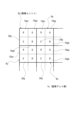
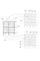
- 4 is a diagram showing an example of a pixel arrangement of a pixel array unit included in a sensor unit according to an embodiment.
- FIG. 4 is a diagram illustrating an example of an internal configuration of an event image generating unit in the embodiment.
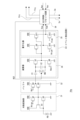
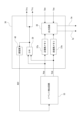
- FIG. FIG. 2 is a diagram illustrating an example of a circuit configuration of an event pixel according to an embodiment. 4 is a diagram for explaining an example of an internal configuration of an output control and reset circuit in the embodiment.
- FIG. FIG. 2 is a diagram illustrating an example of an internal configuration of a sensor unit according to a first embodiment.
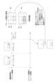
- FIGS. 11A and 11B are diagrams illustrating a comparison between a luminance signal image and an event image according to an embodiment.
- FIG. 4 is an explanatory diagram of a unit area according to the embodiment.
- FIG. 2 is a diagram for explaining an outline of an edge enhancement method according to a first embodiment.
- FIG. 4 is an explanatory diagram of an edge emphasis direction in the embodiment.
- 11A to 11C are diagrams illustrating an example of edge enhancement processing according to an embodiment.
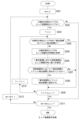
- 10 is a flowchart illustrating an example of a specific processing procedure executed by an emphasis area/emphasis direction detection unit in the embodiment.
- 10 is a flowchart illustrating an example of a specific processing procedure executed by an edge enhancement unit in the embodiment.
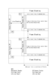
- 11 is a diagram showing an example of how edge emphasis related information is stored in the embodiment.
- FIG. 11A and 11B are diagrams illustrating another example of how edge emphasis related information is stored in the embodiment.
- 13 is a diagram showing yet another example of how edge emphasis related information is stored in the embodiment.
- FIG. 11A and 11B are diagrams for explaining a configuration example and an operation example of an image usage processing unit in the case where edge emphasis related information is used to reduce a calculation load.
- FIG. 11 is a block diagram showing an example of the internal configuration of a sensor unit according to a second embodiment.
- 11A and 11B are diagrams for explaining an example of an operation when edge enhancement of a gradation image is performed based on an edge direction detected based on an event image after edge enhancement.
- FIG. 13 is a block diagram showing an example of the internal configuration of a sensor unit according to a third embodiment.
- FIG. 2 is an explanatory diagram of a binarized image.
- FIG. 13 is a block diagram showing an example of the internal configuration of a sensor unit as a modified example for detecting an edge direction on a binarized image.
- 13A and 13B are explanatory diagrams of modified examples of pixel arrangement patterns in a pixel array portion.
- 13 is a diagram showing an example of the internal configuration of an imaging device as a modified example in which a gray scale sensor and an event sensor are provided separately.
- 25A and 25B are diagrams for explaining examples of the internal configurations of a tone sensor unit and an event sensor unit in the case where the imaging device shown in FIG. 24 is employed.
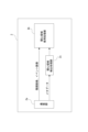
- FIG. 1 is a block diagram showing an example of the internal configuration of an imaging device 100 as a first embodiment configured to include a signal processing device as a first embodiment according to the present technology.
- an imaging device 100 according to the first embodiment includes a sensor unit 1, an image usage processing unit 2, and a communication unit 3.
- the sensor unit 1 has a gradation image generating unit 10 and an event image generating unit 20, and is configured to be capable of generating a gradation image and an event image.
- the gray scale image means an image obtained by a gray scale pixel group having a plurality of gray scale pixels that detect the amount of light received by a light receiving element by a gray scale value of a predetermined number of steps.
- An event image refers to an image that shows the results of detecting an event on a pixel-by-pixel basis, where an event refers to a change in the amount of light received by a light receiving element that is equal to or exceeds a predetermined amount.
- the sensor unit 1 has a configuration as a so-called mixed sensor in which an event pixel group, which has multiple event pixels that detect events, and a gradation pixel group are mixed in the pixel array section 1a.
- FIG. 2 shows an example of a pixel arrangement in the pixel array section 1 a of the sensor section 1 .
- gradation pixels 10g and event pixels 20g for detecting events are arranged in a predetermined arrangement pattern.
- gradation pixels 10gr, 10gg, and 10gb corresponding to the respective colors of R (red), G (green), and B (blue) are formed as the gradation pixels 10g.
- the gradation pixel 10gr is configured to be able to selectively receive R light
- the gradation pixel 10gg is configured to receive G light
- the gradation pixel 10gb is configured to selectively receive B light.
- the pixel array section 1a of this example is formed by arranging a plurality of pixel units Gu, each of which is composed of one gradation pixel 10gr, 10gg, 10gb, and an event pixel 20g, in a two-dimensional predetermined pattern.
- the pixel arrangement pattern in the pixel unit Gu is not limited to this, and other arrangement patterns may also be adopted.
- a plurality of gradation pixels 10g are formed as a gradation pixel group in the pixel array portion 1a, and a plurality of event pixels 20g are formed as an event pixel group.
- light from a subject is incident on the pixel array unit 1a via an imaging lens, so the gradation pixel group and the event pixel group receive light from the subject via a common imaging lens.
- a gradation image generating unit 10 generates a gradation image based on gradation values (light receiving signal values) detected by gradation pixels 10gr, 10gg, and 10gb in a pixel array unit 1a.
- the gradation image generated by the gradation image generating unit 10 is a RAW image before demosaic processing.
- a grayscale image generated as a RAW image by the grayscale image generating unit 10 is subjected to demosaic processing and output as an input image to the image usage processing unit 2 . It is also possible to configure the sensor unit 1 to output a raw image as is, and for the image usage processing unit 2 to perform demosaic processing.
- the event image generator 20 generates an event image that indicates an event detection result by the event detection pixel group in the pixel array unit 1 a.
- the event image is information indicating at least whether an event has occurred for each event pixel 20 g.
- the event image generating unit 20 in this example generates event images at a predetermined frame period. That is, an image indicating whether an event is detected at each event pixel 20g is generated at each fixed frame period.
- the frame period of the event image is set to be shorter than the frame period of the gradation image, and is set to be at least 1/10 of the frame period of the gradation image, for example.
- the event image generating unit 20 in this example is configured to be able to detect, as events, "positive events” which are an increase in the amount of received light of a predetermined amount or more, and "negative events” which are a decrease in the amount of received light of a predetermined amount or more. That is, the event image generated in this case is an image that indicates whether or not a positive event has occurred and whether or not a negative event has occurred for each event pixel 20g.
- the internal configuration of the event image generating unit 20 will be described later.
- the sensor unit 1 is also provided with a circuit unit (an edge enhancing unit 15, described later) that performs edge enhancement processing on the event image generated by the event image generating unit 20, but this will be described later.
- the image usage processing unit 2 performs image analysis processing using as an input image at least the event image output from the sensor unit 1.
- the image usage processing unit 2 performs image analysis processing using as an input image not only the event image but also the gradation image (in this example, the gradation image after demosaic processing) output from the sensor unit 1.
- the image analysis processing here may be processing using AI (artificial intelligence).
- the image analysis process here may include, for example, subject recognition process, movement direction detection process, optical flow analysis process, and the like.
- the communication unit 3 performs wired or wireless data communication with an external device of the imaging device 100. This communication unit 3 makes it possible to output information indicating the image analysis results by the image usage processing unit 2 to the external device of the imaging device 100.
- FIG. 3 is a diagram showing an example of the internal configuration of the event image generating unit 20.
- the event image generating unit 20 includes a plurality of event pixels 20g as an event pixel group in the pixel array unit 1a, an X arbiter 21, a Y arbiter 22, an event processing circuit 23, and an output I/F (interface) 24.
- Each event pixel 20g has a light receiving element and is configured to be able to detect an event that is a change in the amount of received light that is equal to or greater than a predetermined amount.
- each event pixel 20g is configured to be able to detect positive polarity events and negative polarity events as events.
- each event pixel 20g When each event pixel 20g detects an event, regardless of whether it is a positive polarity event or a negative polarity event, it outputs a request signal to request reading (output) of the event signal from itself to the X arbiter 21 and the Y arbiter 22. As shown in the figure, the request signal to the X arbiter 21 is a "request signal Xrq" and the request signal to the Y arbiter 22 is a "request signal Yrq.” Then, each event pixel 20g outputs an event signal according to arbitration by the X arbiter 21 and the Y arbiter 22 in response to the request signals Xrq and Yrq.
- each event pixel 20g outputs a positive event signal Ip, which is a signal indicating the detection result of a positive polarity event, and a negative event signal Im, which is a signal indicating the detection result of a negative polarity event, to the event processing circuit 23 in response to receiving a response signal Xac output by the X arbiter 21 as a response (ACK) to the request signal Xrq and a response signal Yac output by the Y arbiter 22 as a response to the request signal Yrq.
- the X arbiter 21 and the Y arbiter 22 arbitrate the request signals (the above-mentioned request signals Xrq and Yrq) from each event pixel 20g, and transmit a response based on the arbitration result (permission/non-permission of the event signal output) as the above-mentioned response signal (Xac and Yac) to the event pixel 20g that output the request signal.
- the event processing circuit 23 generates event data for the event pixel 20g based on the event signals (in this example, the positive event signal Ip and the negative event signal Im) input from the event pixel 20g.
- the event data generated includes at least position information of the event pixel 20g where the event was detected (address information in the pixel coordinate system: hereinafter referred to as "position information of the event occurrence pixel") and "detection time information" indicating the time when the event was detected.
- the event data generated includes "event type information" which is information indicating the type of the detected event (positive polarity event/negative polarity event) in addition to the position information and detection time information of the event occurrence pixel described above.
- the output I/F 24 sequentially outputs the event data output by the event processing circuit 23 on a row-by-row basis to the outside. From this output I/F 24, an event image indicating the event detection result for each coordinate of the pixel unit Gu is output as shown in the figure.
- FIG. 4 is a diagram showing an example of a circuit configuration of the event pixel 20g.
- the event pixel 20g includes a photodiode PD as a light receiving element, a logarithmic converter 31, a buffer 32, an event detection circuit 33, and an output control and reset circuit .
- the charge accumulated in the photodiode PD is transferred to the logarithmic converter 31.
- the logarithmic converter 31 converts the photocurrent (current corresponding to the amount of received light) obtained by the photodiode PD into a logarithmic voltage signal.
- the buffer 32 corrects the voltage signal input from the logarithmic converter 31 and outputs the corrected voltage signal to the event detection circuit 33 .
- the logarithmic conversion section 31 includes a transistor Q1, a transistor Q2, and a transistor Q3.
- MOSFETs metal-oxide-semiconductor field-effect transistors
- the transistors Q1 and Q3 are N-type transistors, and the transistor Q2 is a P-type transistor.
- the source of the transistor Q1 is connected to the cathode of the photodiode PD, and the drain is connected to a power supply terminal (reference potential VDD).
- the transistors Q2 and Q3 are connected in series between the power supply terminal and the ground terminal.
- the connection point between the transistors Q2 and Q3 is connected to the gate of the transistor Q1 and the input terminal of the buffer 32 (the gate of a transistor Q5 described later).
- a predetermined bias voltage Vbias is applied to the gate of the transistor Q2.
- transistor Q1 and transistor Q3 are connected to the power supply (reference potential VDD), forming a source follower circuit.
- the photocurrent from the photodiode PD is converted into a logarithmic voltage signal by these two source followers connected in a loop.
- Transistor Q2 also supplies a constant current to transistor Q3.
- the buffer 32 includes a transistor Q4 and a transistor Q5, each of which is a P-type transistor, and these transistors Q4 and Q5 are connected in series between a power supply terminal and a ground terminal.
- the connection point between the transistor Q4 and the transistor Q5 serves as the output terminal of the buffer 32, and the corrected voltage signal is output from this output terminal to the event detection circuit 33 as a light reception signal.
- the event detection circuit 33 detects a change in the amount of received light as an event by determining the difference between the current level of the received light signal and the past level of the received light signal as a reference level Lref. Specifically, the event detection circuit 33 detects whether an event has occurred based on whether the level (absolute value) of a differential signal representing the difference between the reference level Lref and the current level of the received light signal is equal to or greater than a predetermined threshold.
- the event detection circuit 33 of this example is configured to be able to detect and distinguish between positive polarity events, i.e., events in which the difference from the reference level Lref is positive, and negative polarity events, i.e., events in which the difference from the reference level Lref is negative.
- the event detection circuit 33 generates a positive output voltage Vop as an output voltage indicative of the detection result of a positive event, and a negative output voltage Vom as an output voltage indicative of the detection result of a negative event.
- the event detection circuit 33 resets the reference level Lref to the current level of the light receiving signal based on a reset signal RST, which will be described later.
- a reset signal RST which will be described later.
- the event detection circuit 33 includes a subtractor 34 and a quantizer 35 .
- the subtractor 34 reduces the level of the light reception signal (voltage signal) from the buffer 32 in accordance with the reset signal RST, and outputs the reduced light reception signal to the quantizer 35 .
- the quantizer 35 quantizes the light reception signal from the subtractor 34, and obtains an output voltage indicating the quantization result. Specifically, in this example, a positive output voltage Vop and a negative output voltage Vom are obtained.
- the subtractor 34 includes a capacitor C1, a capacitor C2, a transistor Q7, a transistor Q8, and a reset switch SWr.
- the transistor Q7 is a P-type transistor
- the transistor Q8 is an N-type transistor.
- the transistors Q7 and Q8 are connected in series between a power supply terminal and a ground terminal to form an inverter. Specifically, the source of the transistor Q7 is connected to the power supply terminal, the drain is connected to the drain of the transistor Q8, and the source of the transistor Q8 is connected to the ground terminal.
- a voltage Vbdif is applied to the gate of the transistor Q8.
- One end of the capacitor C1 is connected to the output terminal of the buffer 32, and the other end is connected to the gate of the transistor Q7 (the input terminal of the inverter).
- the reset switch SWr has one end connected to the connection point between the capacitor C1 and the capacitor C2 and the other end connected to the connection point between the connection point between the transistor Q7 and the transistor Q8 and the capacitor C2, and is connected in parallel to the capacitor C2.
- the reset switch SWr is a switch that is turned ON/OFF in accordance with a reset signal RST.
- the inverter formed by the transistors Q7 and Q8 inverts the light receiving signal input via the capacitor C1 and outputs the inverted signal to the quantizer 35.
- the potential generated on the buffer 32 side of the capacitor C1 at a certain point in time in the subtractor 34 is taken as potential Vinit.
- the reset switch SWr is turned ON.
- the side of the capacitor C1 opposite the buffer 32 becomes a virtual ground terminal.
- the potential of this virtual ground terminal is taken as zero.
- the charge CHinit stored in the capacitor C1 is expressed by the following [Equation 1], where the capacitance of the capacitor C1 is Cp1.
- CHinit Cp1 ⁇ Vinit... [Formula 1]
- both ends of the capacitor C2 are shorted, so that the stored charge therein becomes zero.
- Equation 5 represents the subtraction operation of the voltage signal, and the gain of the subtraction result is Cp1/Cp2.
- the subtractor 34 outputs a signal that represents the difference between the past level (Vinit) of the light receiving signal and the current level (Vafter) of the light receiving signal.
- the potential Vinit corresponds to the above-mentioned reference level Lref.
- the quantizer 35 includes a transistor Q9, a transistor Q10, a transistor Q11, and a transistor Q12, and is configured as a 1.5-bit quantizer.
- the transistors Q9 and Q11 are P-type transistors, and the transistors Q10 and Q12 are N-type transistors.
- transistors Q9 and Q10, and transistors Q11 and Q12 are connected in series between a power supply terminal and a ground terminal, and the output voltage (Vout) of the subtractor 34 is input to the gates of the transistors Q9 and Q11.
- a voltage Vhigh is applied to the gate of the transistor Q10, and a voltage Vlow is applied to the gate of the transistor Q12.
- a positive output voltage Vop indicating the detection result of a positive event is obtained at the connection point between transistor Q9 and transistor Q10, and a negative output voltage Vom indicating the detection result of a negative event is obtained at the connection point between transistor Q11 and transistor Q12.
- a positive output voltage Vop at H level is obtained at the connection point between transistor Q9 and transistor Q10, and when the level of the output voltage of subtractor 34 is lower than the positive threshold value, a positive output voltage Vop at L level is obtained.
- a signal indicating whether the amount of received light has increased by a predetermined threshold value or more, that is, a positive output voltage Vop indicating the detection result of a positive polarity event is obtained. Furthermore, on the side of transistors Q11 and Q12, when the level of the output voltage of subtractor 34 is equal to or lower than the negative threshold value corresponding to voltage Vlow, a negative output voltage Vom at H level is obtained at the connection point between transistors Q11 and Q12, and when the level of the output voltage of subtractor 34 is higher than the negative threshold value, a negative output voltage Vom at L level is obtained.
- a signal indicating whether the amount of received light has changed in the decreasing direction by more than a predetermined threshold value i.e., a negative output voltage Vom indicating the detection result of a negative polarity event, is obtained at the connection point between transistors Q11 and Q12.
- the output control and reset circuit 36 outputs request signals Xrq and Yrq to the X arbiter 21 and Y arbiter 22 described above, outputs a positive event signal Ip and a negative event signal Im in response to response signals Xac and Yac, and outputs a reset signal RST to the reset switch SWr.
- FIG. 5 is a diagram for explaining an example of the internal configuration of the output control and reset circuit 36, and shows the event detection circuit 33 together with the example of the internal configuration of the output control and reset circuit 36.
- the output control and reset circuit 36 includes a positive memory 37 p, a negative memory 37 m, an output circuit 38 , an OR circuit 39 , and a delay device 40 .
- the positive output voltage Vop from the event detection circuit 33 is held in the positive output voltage Vop and is input to the OR circuit 39.
- the negative output voltage Vom from the event detection circuit 33 is held in the negative memory 37m and is input to the OR circuit 39.
- the positive side memory 37p and the negative side memory 37m hold values (digital values) according to the voltage levels of the input positive side output voltage Vop and negative side output voltage Vom. Specifically, in this example, if the voltage levels of the positive side output voltage Vop and the negative side output voltage Vom are H level, "1" is held, and if they are L level, "0" is held.
- the OR circuit 39 outputs an H level signal when at least one of the input positive output voltage Vop and negative output voltage Vom is at H level, and outputs an L level signal when both are at L level. In other words, the OR circuit 39 sets its output signal to H level in response to detection of either a positive event or a negative event, and sets its output signal to L level when neither event is detected.
- Such output signals from the OR circuit 39 are sent to the X arbiter 21 and the Y arbiter 22 as the above-mentioned request signals Xrq and Yrq, respectively.
- the output circuit 38 In response to receiving both the response signal Xac from the X arbiter 21 and the response signal Yac from the Y arbiter 22, the output circuit 38 outputs the value held in the positive side memory 37p and the value held in the negative side memory 37m to the event processing circuit 23 as a positive side event signal Ip and a negative side event signal Im, respectively.
- a positive event is detected, a "1" is output as the positive event signal Ip and a "0" is output as the negative event signal Im, allowing the event processing circuit 23 to determine that a positive event has been detected in the corresponding event pixel 20g.
- the delay unit 40 delays the output signal from the OR circuit 39 and outputs the delayed signal as a reset signal RST to the event detection circuit 33 (reset switch SWr).
- the event detection circuit 33 is reset to a state in which it can detect a new event.
- the delay time of the delay unit 40 should be set to at least the time required for the positive output voltage Vop and the negative output voltage Vom to be held in the positive memory 37p and the negative memory 37m after the positive output voltage Vop and the negative output voltage Vom change to the H level or the L level, respectively. This makes it possible to prevent events from being overlooked.
- the reset of the event detection circuit 33 by the reset signal RST can be configured to be performed at that frame cycle.
- the event image generating unit 20 is configured to generate an event image indicating the occurrence or non-occurrence of an event as a positive polarity event or a negative polarity event for each event pixel 20g (i.e., for each coordinate of the pixel unit Gu) at a predetermined frame period. For example, by collecting event data to which detection time information indicating the time within each frame period is attached, it is possible to generate an event image at a frame period.
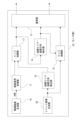
- FIG. 6 is a diagram showing an example of the internal configuration of the sensor unit 1 according to the first embodiment.
- the sensor unit 1 is an embodiment of a signal processing device and a sensor device according to the present technology. As shown in the figure, the sensor unit 1 includes, in addition to the gradation image generating unit 10 and event image generating unit 20 shown in FIG. 1 above, an image signal processing unit 11, a luminance signal conversion unit 12, a communication unit 13, an emphasis area/emphasis direction detection unit 14, and an edge emphasis unit 15.
- the sensor unit 1 is configured as a single semiconductor package by stacking a semiconductor substrate on which a pixel array unit 1a including a gradation pixel group in the gradation image generating unit 10 and an event pixel group in the event image generating unit 20 is formed, and one or more semiconductor substrates on which other circuit units other than the pixel array unit 1a are formed.
- the gradation image based on the RAW image obtained by the gradation image generation unit 10 is input to the image signal processing unit 11.
- the image signal processing unit 11 performs demosaic processing on the gradation image based on the input RAW image to generate an RGB color image.
- the demosaic processing here refers to the process of calculating the luminance values of each of the colors R, G, and B for each pixel position (including the pixel position of the event pixel 20g) in the pixel array unit 1a.
- the communication unit 13 performs data communication in accordance with a predetermined data communication format with an external device of the sensor unit 1, specifically, with the image usage processing unit 2 shown in FIG. 1 in this example.
- the gradation image that has been converted into an RGB color image format by the image signal processing unit 11 is output as an input image to the image usage processing unit 2 via the communication unit 13 .
- the event image generated by the event image generating unit 20 is input to the edge enhancing unit 15 .
- the edge enhancement unit 15 performs edge enhancement processing on the event image input from the event image generation unit 20. Specifically, the edge enhancement unit 15 performs edge enhancement processing on the event image based on the edge direction of the subject detected based on the gradation image generated by the gradation image generation unit 10.
- the edge direction of the subject based on the gradation image is detected by the emphasis area/emphasis direction detection unit 14 based on the luminance signal image generated by the luminance signal conversion unit 12.
- the luminance signal conversion unit 12 generates a luminance signal image (monochrome image) by adding the R, G, and B luminance values for each pixel unit Gu in a predetermined ratio for the gradation image generated by the gradation image generation unit 10.
- FIG. 7 shows a comparison between the luminance signal image obtained by the luminance signal conversion unit 12 and the event image generated by the event image generation unit 20.
- the luminance signal image (the image in the upper right corner in the figure) is generated as an image indicating the value of the luminance signal ("Y") for each coordinate of the pixel unit Gu.
- the event image (the image at the lower right in the figure) is generated as an image indicating the occurrence or non-occurrence of an event (detection or non-occurrence) for each coordinate of the pixel unit Gu.
- the luminance signal conversion unit 12 As described above and configuring the emphasis area/emphasis direction detection unit 14 to perform edge detection based on the luminance signal image, it is possible to reduce the amount of data handled in the edge detection process and to reduce the processing burden related to edge detection, compared to when edge detection is performed based on a demosaiced image.
- the emphasis area/emphasis direction detection unit 14 performs edge detection processing of the subject based on the luminance signal image generated by the luminance signal conversion unit 12, and also performs processing to set edge emphasis unit areas and the edge emphasis direction for each edge emphasis unit area based on the edge detection results.
- FIG. 8 is an explanatory diagram of a unit area As in each of a luminance signal image and an event image.
- an area equivalent to one pixel unit Gu is regarded as one pixel on the image.
- the unit area As means an area consisting of a predetermined number of pixels in each of the luminance signal image and the event image.
- the unit area As is defined as an area in which both the number of horizontal pixels and the number of vertical pixels are multiple.
- the emphasis area/emphasis direction detection unit 14 performs edge detection processing for each unit area As on the luminance signal image, and sets the unit area As in which an edge is detected as an edge emphasis unit area, that is, the unit area As on which the edge emphasis processing should be performed. Furthermore, the emphasis area/emphasis direction detection unit 14 sets the direction of the detected edge as the edge emphasis direction for the edge emphasis unit area.
- the edge enhancement unit 15 performs edge enhancement processing on the event image input from the event image generation unit 20 based on the information indicating the edge enhancement unit area and the information on the edge enhancement direction set for each edge enhancement unit area from the enhancement area/emphasis direction detection unit 14. Specifically, the edge enhancement processing is performed according to the set edge enhancement direction on only the unit areas As in the event image that correspond to the edge enhancement unit areas.
- the event image that has been subjected to edge enhancement processing by the edge enhancement unit 15 is output to the communication unit 13.
- the communication unit 13 also receives information indicating the edge emphasis unit area obtained by the emphasis area/emphasis direction detection unit 14, and information on the edge emphasis direction set for each edge emphasis unit area.
- the communication unit 13 outputs the event image that has been subjected to edge enhancement processing to the image usage processing unit 2 in a data format that conforms to a predetermined data communication format.
- the communication unit 13 in this example performs processing to output edge enhancement-related information based on the information input from the enhancement area/emphasis direction detection unit 14, i.e., information indicating the edge enhancement unit area and information on the edge enhancement direction set for each edge enhancement unit area, as metadata for the event image, the details of which will be explained again later.
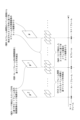
- FIG. 9 is a diagram for explaining an outline of the edge enhancement method according to the first embodiment.
- the relationship between the frame period of the gradation image (i.e., the frame period of the luminance signal image) and the frame period of the event image is illustrated.
- the frame period of the event image is set to be shorter than the frame period of the gradation image.
- detection of edge direction based on a gradation image is performed on an inter-frame difference image of a luminance signal image.
- an inter-frame difference image of the luminance signal image of the N-1th frame and the Nth frame of the gradation image is illustrated, but since only subjects as moving objects are detected in the inter-frame difference image, in the example in the figure, only subjects as cars are detected among subjects as cars (moving objects) and subjects as people (stationary objects) captured in the luminance signal image.
- the range of movement of a vehicle subject as a moving object within the images from the (N-1)th frame to the Nth frame is shown diagrammatically below the inter-frame difference image.
- the emphasis area/emphasis direction detection unit 14 in this example generates an inter-frame difference image of the luminance signal image as described above, performs edge detection for each unit area As targeting the inter-frame difference image, and further sets the edge emphasis unit area and the edge emphasis direction for each edge emphasis unit area based on the edge detection results for each unit area As.
- the edge enhancement unit 15 performs edge enhancement processing on the event image according to the edge enhancement unit area and edge enhancement direction information thus set.
- the edge enhancement unit area and edge enhancement direction information is obtained after the Nth frame gradation image (luminance signal image) has been obtained, so the edge enhancement processing is performed on each event image generated during the frame period of the N+1th frame.
- FIG. 10 is an explanatory diagram of the edge emphasis direction determined for each edge emphasis unit area. As shown in the figure, eight directions are defined as the edge emphasis directions in this example. Specifically, when the horizontal direction of the luminance signal image and the event image is set to 0 degrees, eight directions are defined up to 157.5 degrees in increments of 22.5 degrees. Note that setting the number of edge emphasis directions to eight is merely an example, and the number of edge emphasis directions can be defined arbitrarily.
- the emphasis area/emphasis direction detection unit 14 sets one of these eight directions as the edge emphasis direction according to the direction of the detected edge when setting the edge emphasis direction for each edge emphasis unit area.
- the direction of the dominant edge e.g., the longest edge
- the direction with the largest number of edges when classifying the detected edges by direction as the edge emphasis direction.
- the dominant edge direction in the edge emphasis unit area may be set as the edge emphasis direction.
- FIG. 11 is an explanatory diagram of an example of edge enhancement processing in the embodiment.
- the edge enhancement process is performed by replacing an event non-detection pixel with an event detection pixel when two event detection pixels are separated by an event non-detection pixel in an edge direction (edge enhancement direction) detected based on a gradation image.
- a search range S for edge enhancement is determined in a unit area As serving as an edge enhancement unit area.
- This search range S is determined as a range of multiple pixels aligned in the edge enhancement direction.
- a range of seven pixels aligned in the horizontal direction is determined as the search range S in response to the edge enhancement direction set for the edge enhancement unit area to be processed being the 0 degree direction.
- the search range S is defined as a range centered on the pixel to be processed (target coordinates).
- the edge enhancement process is performed by shifting the pixel to be processed (target coordinates) one by one within the edge enhancement unit area of the event image. Specifically, first it is determined whether the target coordinates are non-event detection coordinates where no event has been detected, and if the target coordinates are non-event detection coordinates, it is determined whether the target coordinates are sandwiched between two event detection coordinates (represented by "E" in the figure) within search range S centered on the target coordinates. If the target coordinates are sandwiched between two event detection coordinates, a process is performed to set the non-event detection coordinates as the target coordinates to the event detection coordinates.
- the edge enhancement unit 15 in this example performs the above-mentioned process for each edge enhancement unit area. This makes it possible to achieve edge enhancement of the event image.
- edge enhancement of the event image is performed separately for the edges of the positive and negative events.
- the edge enhancement process determines whether the processing target coordinate satisfies either the condition that the processing target coordinate is sandwiched between two positive polarity event detection coordinates within the search range S, or the condition that the processing target coordinate is sandwiched between two negative polarity event detection coordinates. If the former condition is satisfied, the processing target coordinate as the event non-detection coordinate is set to the positive polarity event detection coordinate, and if the latter condition is satisfied, the processing target coordinate as the event non-detection coordinate is set to the negative polarity event detection coordinate.
- FIG. 12 is a flowchart showing an example of a specific processing procedure executed by the emphasis area/emphasis direction detection unit 14.
- the emphasis area/emphasis direction detection unit 14 receives a new frame image of a grayscale image. That is, in this example, the frame image of a luminance signal image newly generated by the luminance signal conversion unit 12 is received.
- step S102 the emphasis area/emphasis direction detection unit 14 generates an inter-frame difference image, i.e., an inter-frame difference image of the luminance signal image, and in the subsequent step S103, performs edge detection processing on the difference image (inter-frame difference image).
- step S104 following step S103 the emphasis area/emphasis direction detection unit 14 performs processing to set the unit area in which the edge is detected as an edge emphasis unit area.
- step S105 the emphasis area/emphasis direction detection unit 14 performs a process of setting the direction in which the detected edge faces as the edge emphasis direction for each edge emphasis unit area, and then ends the series of processes shown in Figure 12.
- the details of the process for setting the edge emphasis direction for each edge emphasis unit area have already been explained, so a duplicate explanation will be avoided.
- FIG. 13 is a flowchart showing an example of a specific processing procedure executed by the edge enhancement unit 15.
- the edge enhancement unit 15 resets the unit area identifier M to 0, and in the following step S202, determines whether the M-th unit area As is an edge enhancement unit area. This determination process can be performed based on the information indicating the edge enhancement unit area input from the enhancement area/emphasis direction detection unit 14.
- step S202 If it is determined in step S202 that the Mth unit area As is an edge enhancement unit area, the edge enhancement unit 15 proceeds to step S203, resets the pixel coordinate identifier T to 0, and then in step S204 determines whether the Tth coordinate in the Mth unit area As is an event detection coordinate.
- step S204 If it is determined in step S204 that the Tth coordinate in the Mth unit area As is not an event detection coordinate (i.e., is a non-event detection coordinate), the edge enhancement unit 15 proceeds to step S205, where it acquires edge enhancement direction information for the Mth unit area, and then in the following step S206, it sets the search range S for the Tth coordinate based on the edge enhancement direction.
- step S207 the edge enhancement unit 15 determines whether or not the Tth coordinate is sandwiched between event detection coordinates within the search range S. If the Tth coordinate is sandwiched between event detection coordinates, the process proceeds to step S208, where the Tth coordinate is set as the event detection coordinate, and the process proceeds to step S209.
- step S209 the edge enhancement unit 15 determines whether the pixel coordinate identifier T has reached an upper limit value Tmax.
- the upper limit value Tmax means the total number of pixels in the unit area As (edge enhancement unit area) being processed
- step S209 corresponds to the process of determining whether processing has been performed for all pixels in the edge enhancement unit area being processed.
- the edge enhancement unit 15 increments the pixel coordinate identifier T by 1 in step S210 and then returns to the previous step S204. This makes it possible to execute the processes from step S204 to S208 for a new pixel.
- step S204 determines in step S204 that the Tth coordinate in the Mth unit area As is an event detection coordinate
- the process proceeds to step S209.
- the coordinate to be processed is an event detection coordinate
- step S207 If the edge enhancement unit 15 determines in step S207 that the Tth coordinate is not sandwiched between event detection coordinates within the search range S, the process proceeds to step S209. In other words, if the Tth coordinate is not sandwiched between event detection coordinates within the search range S, the process of setting the target coordinate as the event non-detection coordinate to the event detection coordinate is not performed.
- step S209 determines in step S209 that the pixel coordinate identifier T has reached the upper limit value Tmax
- the process proceeds to step S211 to determine whether the unit area identifier M has reached the upper limit value Mmax.
- the upper limit value Mmax refers to the total number of unit areas As when the event image is divided into unit areas As
- step S211 corresponds to the process of determining whether the process has been performed for all unit areas As.
- step S211 If it is determined in step S211 that the unit area identifier M has not reached the upper limit value Mmax, the edge enhancement unit 15 increments the unit area identifier M by 1 in step S212, and then returns to the previous step S202. As a result, upon completion of the process for one unit area As, the process for the next unit area As is started. Specifically, if it is determined in step S202 that the Mth unit area As is an edge emphasis unit area, the processes in and after step S203 are executed for edge emphasis.
- step S202 if it is determined in step S202 that the M-th unit area As is not an edge enhancement unit area, the edge enhancement unit 15 advances the process to step S211 described above. As a result, the edge enhancement process is not performed on the unit areas As other than the edge enhancement unit areas. Therefore, since the edge enhancement of the event image is not unnecessarily performed on the unit area As where no edge is detected on the gradation image (luminance signal image) side, the accuracy of the edge enhancement process for the event image can be improved. Also, since the edge enhancement process for the unit area As where the edge enhancement process is not required is omitted, the processing load is reduced.
- step S211 If it is determined in step S211 that the unit area identifier M has reached the upper limit value Mmax, the edge enhancement unit 15 ends the series of processes shown in FIG. 13.
- the edge enhancement of the event image can be performed separately for the edges of the positive and negative events.
- edge enhancement processing in this case has already been described, so a duplicate description will be avoided.
- the communication unit 13 in this example performs a process of outputting the edge emphasis related information as metadata of the event image.
- the edge emphasis related information as metadata may be stored in a predetermined data area in a predetermined output unit data such as packet data when the communication unit 13 transmits the event image according to a predetermined data communication format.
- FIG. 14 to 16 are diagrams for explaining examples of storing edge emphasis related information as metadata.
- a storage example of edge emphasis related information corresponding to a case where the communication unit 13 performs data communication according to the MIPI (Mobile Industry Processor Interface) format will be explained here.
- Fig. 14 shows an example of storing edge emphasis related information in an Embedded Data (EMB) area at the beginning of a frame defined in packet data in the MIPI format
- Fig. 15 shows an example of storing edge emphasis related information in an Embedded Data area at the end of a frame defined in the same packet data
- Fig. 16 shows an example of storing edge emphasis related information at the beginning of each line defined in the same packet data.
- EMB Embedded Data
- the edge emphasis related information may include, for example, coordinate information of the edge emphasis unit area and information indicating which unit area is the edge emphasis unit area. This information can be generated by the communication unit 13 based on information indicating the edge emphasis unit area input from the emphasis area/emphasis direction detection unit 14.
- the edge emphasis related information may include information indicating the gradation image from which the edge emphasis direction was detected (for example, a frame number or a time stamp).
- the image usage processing unit 2 can perform corresponding processing such as selecting an image processing method based on the evaluation results of image reliability depending on whether or not edge emphasis is applied in the image analysis processing in which the event image of the corresponding frame is used as the input image, thereby improving the accuracy of the image analysis processing in which the event image is used as the input image.
- the edge emphasis related information may store, for example, information indicating whether or not edge emphasis has been applied to each unit area As. This information indicating whether or not edge emphasis has been applied to each unit area As is information indicating whether or not edge emphasis processing has actually been applied by the edge emphasis unit 15. If information indicating whether edge enhancement has actually been performed is stored in the EMB area at the beginning of the frame, the output will be delayed by one frame. Storing the information in the EMB area at the end of the frame prevents the output from being delayed by one frame, which is advantageous in terms of real-time performance of the image analysis process at the subsequent stage.
- the edge enhancement related information may include information indicating whether or not there is an edge enhancement unit area in the line, and information indicating whether or not edge enhancement is performed for each unit area As in the line.
- ROI region of interest
- the image-use processing unit 2 includes a communication unit 2a, a region-of-interest use processing unit 2b, and a region-of-interest detection processing unit 2c as shown in the figure.
- the communication unit 2a receives the demosaiced gradation image output from the communication unit 3, and packet data of an event image in which edge emphasis related information is stored as metadata, also output from the communication unit 3.
- the communication unit 2a extracts the event image and metadata as edge emphasis related information from the packet data, outputs the demosaiced gradation image and the event image to a region of interest use processing unit 2b, and outputs the metadata (edge emphasis related information) to a region of interest detection processing unit 2c.
- the region of interest detection processing unit 2c detects regions of interest in the gradation image and the event image based on the input edge emphasis related information. Specifically, for each of the gradation image and the event image, image areas that correspond to the edge emphasis unit areas are detected as regions of interest.
- the region-of-interest use processing unit 2b performs image analysis processing on the region of interest detected by the region-of-interest detection processing unit 2c.
- image analysis processing in this case include surveillance processing and facial recognition processing targeting specific subjects such as people and vehicles, SLAM (Simultaneous Localization and Mapping) processing, eye tracking processing, and hand tracking processing.
- SLAM Simultaneous Localization and Mapping
- Second embodiment> Next, a second embodiment will be described.
- edge enhancement is performed reciprocally between the gradation image side and the event image side.
- parts that are similar to parts that have already been described will be given the same reference numerals and description thereof will be omitted.
- FIG. 18 is a block diagram showing an example of the internal configuration of a sensor unit 1A according to the second embodiment.
- the configuration of the imaging device 100 is the same as that of the first embodiment except that a sensor unit 1A is provided instead of the sensor unit 1, and therefore a description with illustrations will be omitted.
- sensor unit 1A differs from sensor unit 1 in that the luminance signal conversion unit 12 is omitted and an emphasis area/emphasis direction detection unit 16 and an edge emphasis unit 17 are added.
- the emphasis area/emphasis direction detection unit 16 detects the edge direction of the subject based on the event image input from the event image generation unit 20. In this example, the emphasis area/emphasis direction detection unit 16 also sets the edge emphasis unit area and the edge emphasis direction for each edge emphasis unit area based on the result of edge detection for each unit area As using a method similar to that used by the emphasis area/emphasis direction detection unit 14.
- the emphasis area/emphasis direction detection unit 16 performs edge detection for each unit area As for one frame of the event image, and sets the edge emphasis unit area and the edge emphasis direction for each edge emphasis unit area based on the result.
- the edge enhancement unit 17 performs edge enhancement processing on the gradation image (RGB color image) after demosaic processing has been performed by the image signal processing unit 11, based on the information indicating the edge enhancement unit area and the information indicating the edge enhancement direction for each edge enhancement unit area obtained by the enhancement area/emphasis direction detection unit 16.
- the edge enhancement unit 17 performs edge enhancement processing on the gradation image after demosaic, based on the edge direction of the subject detected based on the event image.
- the edge enhancement unit 17 performs edge enhancement processing on the demosaic gradation image for each image area equivalent to the edge enhancement unit area set by the enhancement area/enhancement direction detection unit 16 in accordance with information indicating the edge enhancement direction.
- a demosaiced gradation image with edges enhanced by the edge enhancement unit 17 is input to the communication unit 13 and output to the image usage processing unit 2.
- the emphasis area/emphasis direction detection unit 14 detects the edge direction based on the gradation image that has been subjected to edge emphasis processing by the edge emphasis unit 17. Specifically, an inter-frame difference image is generated for the gradation image after edge emphasis processing by the edge emphasis unit 17, edge detection is performed for each image area that corresponds to the unit area As in the inter-frame difference image, and based on the result, the edge emphasis unit area is set and the edge emphasis direction is set for each edge emphasis unit area.
- the edge enhancement unit 15 also performs edge enhancement processing on the event image generated by the event image generation unit 20 in the same manner as in the first embodiment, according to the information indicating the edge enhancement unit area set by the enhancement area/emphasis direction detection unit 14 and the information indicating the edge enhancement direction for each edge enhancement unit area.
- the edge enhancing unit 15 performs edge enhancement processing on the event image based on the edge direction detected based on the image after edge enhancement by the edge enhancing unit 17 that performs edge enhancement on the gradation image. This allows for mutual edge interpolation between the event image side and the gradation image side, thereby enabling a further improvement in the accuracy of edge enhancement processing of the event image.
- the edge enhancement unit 17 enhances the edges of the gradation image based on the edge direction detected based on the event image without edge enhancement.
- FIG. 19 is a diagram for explaining an example of the operation when the edge emphasizing unit 17 performs edge enhancement of a gradation image based on an edge direction detected based on an event image after edge enhancement.
- edge direction detection based on an event image is performed in a frame period of an (N-1)th frame, as shown by ⁇ 1> in the figure.
- the detection of the edge direction based on an event image is performed by the emphasis area/emphasis direction detection unit 16.
- the enhancement area/emphasis direction detection unit 16 is configured to input the event image after edge enhancement processing by the edge enhancement unit 15.
- edge enhancement is performed on the grayscale image of the (N-1)th frame (grayscale image after demosaicing) (edge enhancement unit 17).
- edge direction detection is performed based on the grayscale image of the (N-1)th frame after edge enhancement (emphasis area/emphasis direction detection unit 16).
- edge enhancement is performed on the event image obtained in the frame period of the Nth frame (edge enhancement unit 15). Furthermore, as shown by ⁇ 5>, edge enhancement of the Nth frame gradation image is performed based on the edge direction detected from the event image in the Nth frame period (edge enhancement unit 17).
- mutual edge interpolation between the event image side and the gradation image side can be performed in a form in which the edge enhancement unit 17 enhances the edges of the gradation image based on the edge direction detected based on the event image after edge enhancement. In this case as well, it is possible to further improve the accuracy of the edge enhancement process of the event image.
- edge enhancement processing on the gradation image side has been given in which edge enhancement processing is performed on the demosaiced gradation image, but when a luminance signal conversion unit 12 is provided as in the first embodiment, and a configuration is adopted in which the luminance signal image is output as an input image for the image usage processing unit 2, it is also possible to perform edge enhancement processing on the luminance signal image generated by the luminance signal conversion unit 12.
- a configuration can also be adopted in which the emphasis area/emphasis direction detection unit 14 detects the edge direction based on the luminance signal image generated by the luminance signal conversion unit 12.
- the gradation image obtained by the gradation pixel group is a monochrome image
- demosaic processing there is no need to perform demosaic processing, so it is also possible to perform edge enhancement processing based on the edge direction detected based on the event image on the gradation image obtained by the gradation pixel group itself.
- edge enhancement processing is performed on an event image based on a result of edge detection of a subject based on a gradation image and a result of edge detection of a subject based on an event image.
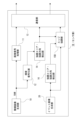
- FIG. 20 is a block diagram showing an example of the internal configuration of a sensor unit 1B according to the third embodiment.
- the configuration of the imaging device 100 is similar to that of the first embodiment except that a sensor unit 1B is provided instead of the sensor unit 1, and therefore a description with illustrations will be omitted.
- sensor unit 1B differs from sensor unit 1 in that it has an emphasis area/emphasis direction detection unit 16 added, and in that edge emphasis unit 15B has been provided instead of edge emphasis unit 15.
- the emphasis area/emphasis direction detection unit 16 inputs the event image generated by the event image generation unit 20, performs edge detection for each unit area As, and sets the edge emphasis unit area and the edge emphasis direction for each edge emphasis unit area based on the results of the edge detection.
- the edge enhancement unit 15B performs edge enhancement processing on the event image based on the subject edge detection result based on the gradation image obtained by the enhancement area/emphasis direction detection unit 14 and the subject edge detection result based on the event image obtained by the enhancement area/emphasis direction detection unit 16.
- the edge enhancement unit 15B performs edge enhancement processing based on information about the edge enhancement direction for each unit area As, the unit area As having an edge detected by either one of the enhancement area and emphasis direction detection units 14, 16.
- the specific processing may be to perform edge enhancement processing based on information about the edge enhancement direction for both the edge enhancement unit area set by the enhancement area and emphasis direction detection unit 14 and the edge enhancement unit area set by the enhancement area and emphasis direction detection unit 16.
- edge emphasis processing based on information about the edge emphasis direction for unit areas As in which edges are detected by both emphasis area/emphasis direction detection units 14 and 16.
- the emphasis area/emphasis direction detection section 14 and the emphasis area/emphasis direction detection section 16 set different edge emphasis directions for the same edge emphasis unit area.
- the edges detected based on an event image and edges detected based on a gradation image are relatively more reliable. Therefore, when different edge emphasis directions are set in this manner, it is possible to adopt the edge emphasis direction determined by the emphasis area/emphasis direction detection unit 14 rather than the edge emphasis direction determined by the emphasis area/emphasis direction detection unit 16, which is less reliable.
- edge direction detection can also be performed on a gradation image (e.g., in the case of a monochrome image), or a binary image of an image generated based on a gradation image, such as a gradation image or luminance signal image after demosaicing.
- the binarized image can be an image in which subjects in the background have been removed and only subjects in the foreground have been extracted, making it suitable for performing edge enhancement on subjects that may be moving objects moving in the foreground of the background, for example.
- Fig. 21 shows an example of a binarized image (the image on the left in the figure) obtained by performing binarization processing on the image of the Nth frame shown in Fig. 9.
- edge detection is performed on this binarized image to set the edge enhancement unit area
- the unit area As shown by the matte finish in the figure is set as the edge enhancement unit area.
- FIG. 22 is a block diagram showing an example of the internal configuration of a sensor unit 1C as a modified example for detecting an edge direction on such a binarized image.
- an example of a configuration in which edge direction detection is performed on a luminance signal image generated by the luminance signal conversion unit 12 is shown.
- the sensor unit 1C differs from the sensor unit 1 in that an emphasis area/emphasis direction detector 14C is provided instead of the emphasis area/emphasis direction detector 14.
- the emphasis area/emphasis direction detection unit 14C binarizes the luminance signal image generated by the luminance signal conversion unit 12, and performs edge detection for each unit area As on the binary image obtained by the binarization, sets an edge emphasis unit area based on the results of the edge detection, and sets the edge emphasis direction for each edge emphasis unit area.
- the pixel array pattern in the pixel array section 1a may also be a pattern in which multiple pixel units Gu′, each of which has 32 R, G, and B gradation pixels and 1 event pixel, are arranged two-dimensionally, as exemplified in FIG. 23.
- the pixel unit Gu' is a pixel unit in which three four-pixel Bayer array pixel units using RGGB are arranged in the horizontal and vertical directions, and a one-pixel event pixel is arranged in a central area the size of four pixels.
- the above example shows a configuration as a so-called mixed sensor, which has a pixel array section 1a in which a group of gradation pixels and a group of event pixels are mixed, but this technology can also be suitably applied to cases in which the gradation sensor and the event sensor are separate.
- the imaging device is configured to separately include a gradation sensor unit 1S having a gradation image generating unit 10 for obtaining a gradation image, and an event sensor unit 1I having an event image generating unit 20 for obtaining an event image.
- the gradation sensor unit 1S has a pixel array section in which a group of gradation pixels is arranged as a pixel array section, and the gradation image generating unit 10 generates a gradation image based on the gradation values detected by the group of gradation pixels in the pixel array section.
- the event sensor unit 1I also has a pixel array unit (hereinafter referred to as pixel array unit 1a') in which a group of event pixels is arranged as a pixel array unit, and the event image generating unit 20 generates an event image based on the event detection results by the group of event pixels in the pixel array unit 1a'.
- pixel array unit 1a' a pixel array unit in which a group of event pixels is arranged as a pixel array unit
- the event image generating unit 20 generates an event image based on the event detection results by the group of event pixels in the pixel array unit 1a'.
- the pixel array unit in each sensor receives light from the subject via different imaging lenses. Therefore, when edge enhancement processing of the event image is performed based on the edge direction detected based on the gradation image, a coordinate alignment process is performed between the gradation image and the event image.
- FIG. 25 is a diagram for explaining an example of the internal configuration of each of the tone sensor unit 1S and the event sensor unit 1I in the case where the imaging device 100D shown in FIG. 24 is adopted.
- the imaging device 100D shown in FIG. 24 it is necessary to synchronize the frame periods between the gradation sensor unit 1S and the event sensor unit 1I, so a synchronization signal Sync is shared between the gradation sensor unit 1S and the event sensor unit 1I as shown in the figure.
- the gradation sensor unit 1S includes a gradation image generating unit 10, an image signal processing unit 11, a luminance signal converting unit 12, a gradation area/emphasis direction detecting unit 14, and a communication unit 13S.
- the event sensor unit 1I also includes an event image generating unit 20, an edge enhancing unit 15, and a communication unit 13I.
- the gradation sensor unit 1S and the event sensor unit 1I are provided separately, it is possible that information indicating the edge emphasis unit area set by the emphasis area/emphasis direction detection unit 14 and information on the edge emphasis direction for each edge emphasis unit area cannot be transmitted directly from the gradation sensor unit 1S to the edge emphasis unit 15 in the event sensor unit 1I.
- information indicating the edge emphasis unit area set by the emphasis area/emphasis direction detection unit 14, and information on the edge emphasis direction for each edge emphasis unit area can be output to the downstream image usage processing unit 2 via the communication unit 13S, and the image usage processing unit 2 can transfer it to the edge emphasis unit 15.
- the communication unit 13S when such a configuration is adopted, it is also possible to configure the communication unit 13S to output metadata as edge enhancement related information as metadata of the gradation image after demosaicing by the image signal processing unit 11 (particularly when the metadata is the presence or absence of an edge enhancement unit area and coordinate information).
- the edge enhancement related information may be output by the communication unit 13I as metadata of the event image after edge enhancement.
- the image usage processing unit 2 performs edge direction detection based on the gradation image and outputs the result to the event sensor unit 1I.
- the signal processing circuit section including the edge enhancement section 15 performs edge enhancement processing on the event image output from the event sensor having the pixel array section in which the event pixel group is arranged.
- the edges of the event image are enhanced (interpolated), so that even if the number of active event pixels is thinned out, an appropriate event image with the missing parts interpolated can be obtained.
- the number of active event pixels is thinned out, so that the power consumption of the sensor can be reduced.
- the amount of event data to be handled is reduced, so that the power consumption of the signal processing unit that handles the event data can be reduced.
- the signal processing device (sensor unit 1, 1A, 1B, 1C, event sensor unit 1I) of the embodiment inputs an event image, which is an image showing the event detection result by an event detection pixel group having a plurality of event pixels that detects a change in the amount of light received by a light receiving element of a predetermined amount or more as an event, and is equipped with a first edge enhancement unit (edge enhancement unit 15, 15B) that performs edge enhancement processing of the event image based on the edge direction of the subject detected based on the gradation image obtained by a gradation pixel group having a plurality of gradation pixels that detects the amount of light received by the light receiving element using a gradation value of a predetermined number of levels.
- edge enhancement unit edge enhancement unit 15, 15B
- edge enhancement processing By performing edge enhancement processing on the event image based on the edge direction of the subject detected based on the gradation image as described above, it becomes possible to appropriately interpolate only the missing portions of the subject's edges. Therefore, it is possible to improve the accuracy of edge enhancement processing of the event image.
- the first edge enhancement unit when two event detection pixels are spaced apart via an event non-detection pixel in an edge direction detected based on a gradation image, performs edge enhancement by replacing the event non-detection pixel with an event detection pixel. This makes it possible to appropriately emphasize the edges of the subject in the event image based on the edge direction of the subject detected based on the gradation image.
- the first edge enhancement unit inputs information indicating an edge enhancement unit area, which is a unit area in which an edge of a subject is detected, among each unit area obtained when a gradation-based image (inter-frame difference image, binary image), which is an image based on a gradation image, is divided into unit areas (same As) consisting of a predetermined number of pixels, and performs edge enhancement processing only on the unit areas that correspond to the edge enhancement unit areas in the event image. This prevents unnecessary edge enhancement of the event image from being performed on unit areas where no edges are detected on the tone-based image side. Therefore, the accuracy of the edge enhancement process for the event image can be improved.
- an edge enhancement unit area which is a unit area in which an edge of a subject is detected, among each unit area obtained when a gradation-based image (inter-frame difference image, binary image), which is an image based on a gradation image, is divided into unit areas (same As) consisting of a predetermined number of pixels, and performs edge enhancement processing only
- the first edge emphasizing section performs edge enhancement processing for each unit area of the event image based on the edge direction detected for each edge enhancement unit area.
- the processing unit for edge enhancement is a unit for each unit area consisting of a predetermined number of pixels, and efficient edge enhancement processing can be realized with a reduced computational load required for edge enhancement.
- the gray-scale-based image is an inter-frame difference image of the gray-scale image. Since only the subject as a moving object is detected in the inter-frame difference image, the edge enhancement unit area in this case is set as a unit area in which only the edges of the subject as a moving object are detected. Therefore, it is possible to prevent edge enhancement of the event image from being performed in response to unnecessary edges, such as the edges of the subject in the background, and it is possible to improve the accuracy of edge enhancement.
- the gradation-based image is a binarized image.
- edge detection By performing edge detection on the binarized image, it is possible to prevent the edges of the subject from being detected in the background portion. Therefore, it is possible to prevent edge enhancement of the event image from being performed in response to unnecessary edges, and it is possible to improve the accuracy of edge enhancement.
- a second edge enhancement unit (edge enhancement unit 17) which performs edge enhancement processing on a gradation image or a gradation-based image which is an image based on a gradation image, based on the edge direction of the subject detected based on the event image, and the first edge enhancement unit performs edge enhancement processing on the event image based on the edge direction detected based on the image edge-enhanced by the second edge enhancement unit.
- This allows for mutual edge interpolation between the event image side and the gradation image side. Therefore, it is possible to further improve the accuracy of edge enhancement processing of the event image.
- a first edge enhancement unit performs edge enhancement processing of the event image based on the result of edge detection of the subject based on the gradation image and the result of edge detection of the subject based on the event image.
- the signal processing device as the embodiment includes a communication unit (13, 13I) that outputs edge enhancement related information, which is information related to the edge enhancement process by the first edge enhancement unit, as metadata of the event image.
- edge enhancement related information which is information related to the edge enhancement process by the first edge enhancement unit, as metadata of the event image.
- the execution unit of the image processing at the subsequent stage can perform corresponding processing to improve the accuracy and efficiency of image processing, such as selecting an image processing method based on the edge enhancement-related information, for example, based on the evaluation results of image reliability depending on whether or not edge enhancement is performed, or excluding image areas where edge enhancement is not performed as areas where no subject is present from the target of image processing, thereby making it possible to improve the accuracy and efficiency of image processing performed using an event image as an input image.
- a first edge enhancement unit inputs information indicating an edge enhancement unit area, which is a unit area in which an edge of a subject is detected, among each unit area obtained when a gradation-based image, which is an image based on a gradation image, is divided into unit areas consisting of a predetermined number of pixels, and performs edge enhancement processing only on unit areas that correspond to the edge enhancement unit areas in the event image, and the edge enhancement related information includes at least one of information indicating which unit areas in the event image are edge enhancement unit areas and information indicating the presence or absence of edge enhancement for each unit area in the event image.
- the event detection pixel group and the gradation pixel group are formed in the same image array unit (sensor unit 1a). This makes it possible to eliminate the need to perform a process of aligning the coordinates between the gradation image and the event image when performing edge enhancement processing on the event image based on the edge direction detected based on the gradation image. Therefore, the processing load required for implementing edge enhancement processing of an event image can be reduced.
- the signal processing device includes an edge detection section (emphasis area/emphasis direction detection section 14, 14C) that detects an edge direction based on a gradation image. That is, a first edge enhancing section that performs edge enhancement processing of an event image and an edge detecting section that detects the edge direction of a subject based on a gradation image are provided in the same signal processing device. This eliminates the need to adopt a configuration in which edge direction information used for edge enhancement processing of event images is transferred from another device to the signal processing device, and eliminates the need to perform communication processing with an external device to realize edge enhancement processing of event images, thereby reducing the processing burden.
- edge detection section emphasis area/emphasis direction detection section 14, 14C
- a signal processing method as an embodiment is a signal processing method in which a signal processing device inputs an event image, which is an image showing an event detection result by an event detection pixel group having a plurality of event pixels that detects a change in the amount of light received by a light receiving element that is equal to or greater than a predetermined amount, as an event, and performs edge enhancement processing of the event image based on the edge direction of a subject detected based on a gradation image obtained by a gradation pixel group having a plurality of gradation pixels that detects the amount of light received by the light receiving element using gradation values of a predetermined number of levels.
- the sensor device includes a pixel array unit (sensor unit 1a, 1a') in which an event detection pixel group is formed having a plurality of event pixels that detect a change in the amount of light received by a light receiving element of a predetermined amount or more as an event, and a first edge enhancement unit (edge enhancement unit 15, 15B) that inputs an event image which is an image showing the event detection result by the event detection pixel group in the pixel array unit, and performs edge enhancement processing of the event image based on the edge direction of the subject detected based on the gradation image obtained by the gradation pixel group having a plurality of gradation pixels that detect the amount of light received by the light receiving element by a predetermined number of gradation values.
- a sensor device it is possible to obtain the same functions and effects as the signal processing device according to the above embodiment.
- a signal processing device comprising: a first edge enhancement unit that inputs an event image, which is an image showing an event detection result by an event detection pixel group having a plurality of event pixels that detects a change of a predetermined amount or more in the amount of light received by a light receiving element as an event, and performs edge enhancement processing on the event image based on an edge direction of a subject detected based on a gradation image obtained by a gradation pixel group having a plurality of gradation pixels that detects the amount of light received by the light receiving element by a predetermined number of gradation values.
- the first edge enhancement unit is The signal processing device described in (1) performs edge enhancement by replacing an event non-detection pixel with an event detection pixel when two event detection pixels are separated by an event non-detection pixel in the edge direction detected based on the gradation image.
- the first edge enhancement unit is The signal processing device according to (1) or (2), wherein information indicating an edge enhancement unit area, which is a unit area in which an edge of a subject is detected among each of the unit areas obtained by dividing a gradation-based image, which is an image based on the gradation image, into unit areas each consisting of a predetermined number of pixels, is input, and the edge enhancement processing is performed only on unit areas corresponding to the edge enhancement unit areas in the event image.
- the first edge enhancement unit is The signal processing device according to (3), wherein the edge enhancement process is performed for each unit area of the event image based on the edge direction detected for each of the edge enhancement unit areas.
- the signal processing device according to (3) or (4), wherein the gradation-based image is an inter-frame difference image of the gradation image.
- the signal processing device according to (3) or (4), wherein the gradation-based image is a binarized image.
- a second edge enhancement unit that performs edge enhancement processing on the gradation image or a gradation-based image that is an image based on the gradation image, based on an edge direction of an object detected based on the event image;
- the first edge enhancement unit is The signal processing device according to any one of (1) to (6), further comprising: performing edge enhancement processing on the event image based on the edge direction detected based on the image edge-enhanced by the second edge enhancement unit.
- the first edge enhancement unit is The signal processing device according to any one of (1) to (7), further comprising: performing edge enhancement processing on the event image based on a result of edge detection of the object based on the gradation image and a result of edge detection of the object based on the event image.
- the signal processing device according to any one of (1) to (8), further comprising a communication unit configured to output edge enhancement related information, which is information related to the edge enhancement process performed by the first edge enhancement unit, as metadata of the event image.
- the first edge enhancement unit is inputting information indicating an edge enhancement unit area, which is an area in which an edge of a subject is detected, among each of the unit areas obtained by dividing a gradation-based image, which is an image based on the gradation image, into a unit area consisting of a predetermined number of pixels, and performing the edge enhancement process only on the unit areas corresponding to the edge enhancement unit areas in the event image;
- the edge enhancement related information is The signal processing device according to (9), further comprising at least one of information indicating which of the unit areas in the event image is the edge-emphasized unit area, and information indicating whether or not edge enhancement is performed for each of the unit areas in the event image.
- a signal processing device comprising: inputting an event image which is an image showing an event detection result by an event detection pixel group having a plurality of event pixels which detects a change in the amount of light received by a light receiving element that is equal to or greater than a predetermined amount as an event; and performing edge enhancement processing on the event image based on an edge direction of a subject detected based on a gradation image obtained by a gradation pixel group having a plurality of gradation pixels which detects the amount of light received by the light receiving element by a gradation value of a predetermined number of levels.
- a pixel array section in which an event detection pixel group is formed, the event detection pixel group including a plurality of event pixels that detect a change in the amount of light received by a light receiving element that is equal to or greater than a predetermined amount as an event; a first edge enhancement unit that inputs an event image which is an image showing an event detection result by the event detection pixel group in the pixel array unit, and performs edge enhancement processing on the event image based on an edge direction of a subject detected based on a gradation image obtained by a gradation pixel group having a plurality of gradation pixels which detect an amount of light received by a light receiving element by a gradation value of a predetermined number of levels.
Landscapes
- Engineering & Computer Science (AREA)
- Multimedia (AREA)
- Signal Processing (AREA)
- Image Processing (AREA)
- Transforming Light Signals Into Electric Signals (AREA)
- Studio Devices (AREA)
Abstract
本技術に係る信号処理装置は、受光素子による受光量の所定量以上の変化をイベントとして検出するイベント画素を複数有して成るイベント検出画素群によるイベント検出結果を示す画像であるイベント画像を入力すると共に、受光素子による受光量を所定階数の階調値により検出する階調画素を複数有して成る階調画素群により得られる階調画像に基づいて検出された被写体のエッジ方向に基づき、イベント画像のエッジ強調処理を行う第一エッジ強調部を備えている。
Description
本技術は、信号処理装置とその方法、及びセンサ装置に関するものであり、特には、受光量の所定量以上の変化をイベントとして検出するイベント検出画素群によるイベント検出結果を示す画像であるイベント画像を対象とした画像信号処理の技術分野に関する。
画像センシングを行う画像センサとして、一般的なカメラに搭載されるイメージセンサ、具体的には、受光素子による受光量を所定階数の階調値により検出する階調画素を複数有して成る階調画素群を画素アレイ部として備える画像センサ(以下「階調センサ」と表記する)が広く知られている。
また、画像センサとしては、階調センサ以外にも、いわゆるEVS(Event based Vision Sensor)として知られるような、受光素子による受光量の所定量以上の変化をイベントとして検出するイベント画素を複数有して成るイベント検出画素群を画素アレイ部として備える画像センサ(以下「イベントセンサ」と表記する)も知られている。
また、画像センサとしては、階調センサ以外にも、いわゆるEVS(Event based Vision Sensor)として知られるような、受光素子による受光量の所定量以上の変化をイベントとして検出するイベント画素を複数有して成るイベント検出画素群を画素アレイ部として備える画像センサ(以下「イベントセンサ」と表記する)も知られている。
ここで、イベントセンサにおいては、例えば、移動物体としての前景被写体とその背景被写体とが同系色である場合や暗所でのセンシングを行った場合等に、前景被写体と背景被写体との間の十分なコントラストが得られないことに起因して、イベント(所定量以上の受光量変化)が発生したはずの画素のうち少なくとも一部の画素でイベントが非検出となってしまい、イベント画像において、イベントの検出漏れ部分、換言すれば欠落部分が生じてしまうことがある。
確認のため述べておくと、ここで言う「イベント画像」とは、イベント検出画素群によるイベント検出結果を示す画像を意味するものであり、具体的には、画素位置ごとにイベントの検出有無を表す情報が対応づけられた情報を意味する。
イベント画像における欠落部分は、主に、移動物体としての被写体の輪郭等のエッジ部分の一部(又は全部)の欠落として生じるものとなる。
確認のため述べておくと、ここで言う「イベント画像」とは、イベント検出画素群によるイベント検出結果を示す画像を意味するものであり、具体的には、画素位置ごとにイベントの検出有無を表す情報が対応づけられた情報を意味する。
イベント画像における欠落部分は、主に、移動物体としての被写体の輪郭等のエッジ部分の一部(又は全部)の欠落として生じるものとなる。
近年では、被写体の認識処理や移動方向の検出処理、オプティカルフロー解析等の各種画像解析処理を、イベント画像を入力画像として実行するシステムも存在し、そのような場合、イベント画像に上記のような欠落部分(エッジ部分の欠落)が生じてしまうと、画像解析処理の精度低下を招いてしまう。
関連する従来技術については、下記特許文献1を挙げることができる。
この特許文献1には、イベントセンサが、イベントの検出のみでなく、イベントが検出された画素における受光信号(輝度値)を読み出して階調画像を生成するように構成された場合において、該階調画像に生じる欠落部分を補間する技術が開示されている。具体的には、イベントが検出された画素から読み出した輝度値により構成される画像データ(画像データG0)と、イベントが検出された画素以外の画素について周期的な読み出しを行って得られる輝度値により構成される画像データ(画像データG1)とをフレームメモリにおいて重ね合わせることで、画像データG0に生じる欠落部分を画像データG1により補間するものである。
この特許文献1には、イベントセンサが、イベントの検出のみでなく、イベントが検出された画素における受光信号(輝度値)を読み出して階調画像を生成するように構成された場合において、該階調画像に生じる欠落部分を補間する技術が開示されている。具体的には、イベントが検出された画素から読み出した輝度値により構成される画像データ(画像データG0)と、イベントが検出された画素以外の画素について周期的な読み出しを行って得られる輝度値により構成される画像データ(画像データG1)とをフレームメモリにおいて重ね合わせることで、画像データG0に生じる欠落部分を画像データG1により補間するものである。
ここで、特許文献1に記載の補間手法は、あくまで階調画像の欠落部分の補間手法であって、イベント画像の欠落部分を補間できるものではない。
また、特許文献1では、画像データG0に対し画像データG1を重ね合わせて欠落部分を補間する手法を採っているので、被写体の輪郭等のエッジ以外の部分も補間される場合もあり、適切なエッジ強調を行うことができない虞がある。
また、特許文献1では、画像データG0に対し画像データG1を重ね合わせて欠落部分を補間する手法を採っているので、被写体の輪郭等のエッジ以外の部分も補間される場合もあり、適切なエッジ強調を行うことができない虞がある。
本技術は上記事情に鑑み為されたものであり、イベント画像のエッジ強調処理について精度向上を図ることを目的とする。
本技術に係る信号処理装置は、受光素子による受光量の所定量以上の変化をイベントとして検出するイベント画素を複数有して成るイベント検出画素群によるイベント検出結果を示す画像であるイベント画像を入力すると共に、受光素子による受光量を所定階数の階調値により検出する階調画素を複数有して成る階調画素群により得られる階調画像に基づいて検出された被写体のエッジ方向に基づき、前記イベント画像のエッジ強調処理を行う第一エッジ強調部を備えたものである。
上記のように階調画像に基づいて検出された被写体のエッジ方向に基づきイベント画像のエッジ強調処理を行うことで、被写体のエッジの欠落部分のみを適切に補間することが可能となる。
上記のように階調画像に基づいて検出された被写体のエッジ方向に基づきイベント画像のエッジ強調処理を行うことで、被写体のエッジの欠落部分のみを適切に補間することが可能となる。
また、本技術に係る信号処理方法は、信号処理装置が、受光素子による受光量の所定量以上の変化をイベントとして検出するイベント画素を複数有して成るイベント検出画素群によるイベント検出結果を示す画像であるイベント画像を入力すると共に、受光素子による受光量を所定階数の階調値により検出する階調画素を複数有して成る階調画素群により得られる階調画像に基づいて検出された被写体のエッジ方向に基づき、前記イベント画像のエッジ強調処理を行う信号処理方法である。
このような信号処理方法により、上記した本技術に係る信号処理装置を実現可能となる。
このような信号処理方法により、上記した本技術に係る信号処理装置を実現可能となる。
さらに、本技術に係るセンサ装置は、受光素子による受光量の所定量以上の変化をイベントとして検出するイベント画素を複数有して成るイベント検出画素群が形成された画素アレイ部と、前記画素アレイ部における前記イベント検出画素群によるイベント検出結果を示す画像であるイベント画像を入力すると共に、受光素子による受光量を所定階数の階調値により検出する階調画素を複数有して成る階調画素群により得られる階調画像に基づいて検出された被写体のエッジ方向に基づき、前記イベント画像のエッジ強調処理を行う第一エッジ強調部と、を備えたものである。
このようなセンサ装置によっても、上記した本技術に係る信号処理装置と同様の作用を得ることが可能である。
このようなセンサ装置によっても、上記した本技術に係る信号処理装置と同様の作用を得ることが可能である。
以下、添付図面を参照し、本技術に係る実施形態を次の順序で説明する。
<1.第一実施形態>
(1-1.撮像装置の構成)
(1-2.第一実施形態としてのセンサ部)
(1-3.処理手順)
(1-4.エッジ強調関連情報について)
<2.第二実施形態>
<3.第三実施形態>
<4.変形例>
<5.実施形態のまとめ>
<6.本技術>
<1.第一実施形態>
(1-1.撮像装置の構成)
(1-2.第一実施形態としてのセンサ部)
(1-3.処理手順)
(1-4.エッジ強調関連情報について)
<2.第二実施形態>
<3.第三実施形態>
<4.変形例>
<5.実施形態のまとめ>
<6.本技術>
<1.第一実施形態>
(1-1.撮像装置の構成)
図1は、本技術に係る第一実施形態としての信号処理装置を備えて構成された第一実施形態としての撮像装置100の内部構成例を示したブロック図である。
図1に示すように第一実施形態としての撮像装置100は、センサ部1と、画像使用処理部2と、通信部3とを備えている。
(1-1.撮像装置の構成)
図1は、本技術に係る第一実施形態としての信号処理装置を備えて構成された第一実施形態としての撮像装置100の内部構成例を示したブロック図である。
図1に示すように第一実施形態としての撮像装置100は、センサ部1と、画像使用処理部2と、通信部3とを備えている。
センサ部1は、階調画像生成部10とイベント画像生成部20とを有し、階調画像とイベント画像とを生成可能に構成されている。
ここで、階調画像とは、受光素子による受光量を所定階数の階調値により検出する階調画素を複数有して成る階調画素群により得られる画像を意味する。
また、イベント画像とは、画素単位でイベントの検出結果を示す画像を意味する。ここで言うイベントとは、受光素子による受光量の所定量以上の変化を意味する。
ここで、階調画像とは、受光素子による受光量を所定階数の階調値により検出する階調画素を複数有して成る階調画素群により得られる画像を意味する。
また、イベント画像とは、画素単位でイベントの検出結果を示す画像を意味する。ここで言うイベントとは、受光素子による受光量の所定量以上の変化を意味する。
本実施形態において、センサ部1は、画素アレイ部1aにおいて、イベントを検出するイベント画素を複数有して成るイベント画素群と階調画素群とが混載された、いわゆる混載センサとしての構成を有する。
図2は、センサ部1が有する画素アレイ部1aの画素配列例を示している。
図示のように画素アレイ部1aにおいては、階調画素10gと、イベントを検出するイベント画素20gとが所定の配列パターンにより配列されている。本例では、階調画像としてカラー画像の生成を可能とするために、階調画素10gとしてはR(赤色)、G(緑色)、B(青色)の各色に対応した階調画素10gr、10gg、10gbが形成されている。階調画素10grはR光を、階調画素10ggはG光を、階調画素10gbはB光をそれぞれ選択的に受光可能に構成されている。
図示のように画素アレイ部1aにおいては、階調画素10gと、イベントを検出するイベント画素20gとが所定の配列パターンにより配列されている。本例では、階調画像としてカラー画像の生成を可能とするために、階調画素10gとしてはR(赤色)、G(緑色)、B(青色)の各色に対応した階調画素10gr、10gg、10gbが形成されている。階調画素10grはR光を、階調画素10ggはG光を、階調画素10gbはB光をそれぞれ選択的に受光可能に構成されている。
本例の画素アレイ部1aは、各一つの階調画素10gr、10gg、10gb、及びイベント画素20gが二次元に所定パターンで配列されて成る画素ユニットGuが、二次元に複数配列されて形成されている。具体的に、本例における画素ユニットGuは、水平方向(水平ライン方向)画素数×垂直方向画素数=2×2=4画素で成り、階調画素10grと階調画素10gg、イベント画素20gと階調画素10gbがそれぞれ水平方向に隣接配置され、且つ階調画素10grとイベント画素20g、階調画素10ggと階調画素10gbがそれぞれ垂直方向に隣接配置されて成る。
なお、画素ユニットGuにおける画素配列パターンはこれに限定されるものではなく、他の配列パターンを採用することも考えられる。
なお、画素ユニットGuにおける画素配列パターンはこれに限定されるものではなく、他の配列パターンを採用することも考えられる。
図2を参照して分かるように、本例のセンサ部1においては、複数の階調画素10gが階調画素群として画素アレイ部1aに形成され、また複数のイベント画素20gがイベント画素群として形成されている。
図示は省略したが、画素アレイ部1aには撮像レンズを介して被写体からの光が入射されるため、階調画素群及びイベント画素群は、共通の撮像レンズを介して被写体からの光を受光する。
図示は省略したが、画素アレイ部1aには撮像レンズを介して被写体からの光が入射されるため、階調画素群及びイベント画素群は、共通の撮像レンズを介して被写体からの光を受光する。
図1において、階調画像生成部10は、画素アレイ部1aにおける階調画素10gr、10gg、10gbにより検出される階調値(受光信号値)に基づき、階調画像を生成する。階調画像生成部10が生成する階調画像は、本例では、デモザイク処理前のRAW画像であるとする。
後述もするように本例のセンサ部1では、階調画像生成部10が生成したRAW画像としての階調画像がデモザイク処理されて画像使用処理部2の入力画像として出力される。
なお、センサ部1からはRAW画像のまま出力し、画像使用処理部2側でデモザイク処理を施す構成とすることも考えられる。
後述もするように本例のセンサ部1では、階調画像生成部10が生成したRAW画像としての階調画像がデモザイク処理されて画像使用処理部2の入力画像として出力される。
なお、センサ部1からはRAW画像のまま出力し、画像使用処理部2側でデモザイク処理を施す構成とすることも考えられる。
イベント画像生成部20は、画素アレイ部1aにおけるイベント検出画素群によるイベント検出結果を示す画像であるイベント画像を生成する。具体的に、イベント画像は、イベント画素20gごとに少なくともイベントの発生有無を示す情報とされる。
本例におけるイベント画像生成部20は、イベント画像を所定のフレーム周期で生成する。すなわち、フレーム期間としての一定期間ごとに、各イベント画素20gにおけるイベント検出有無を示す画像を生成するものである。本例において、イベント画像のフレーム周期は、階調画像のフレーム周期よりも短周期とされ、例えば、階調画像のフレーム周期の少なくとも1/10以下等とされる。
本例におけるイベント画像生成部20は、イベント画像を所定のフレーム周期で生成する。すなわち、フレーム期間としての一定期間ごとに、各イベント画素20gにおけるイベント検出有無を示す画像を生成するものである。本例において、イベント画像のフレーム周期は、階調画像のフレーム周期よりも短周期とされ、例えば、階調画像のフレーム周期の少なくとも1/10以下等とされる。
また、本例におけるイベント画像生成部20は、イベントとして、受光量の所定量以上の増大側変化である「正極性イベント」と、受光量の所定量以上の減少側変化である「負極性イベント」とを検出可能に構成されている。すなわち、この場合のイベント画像としては、イベント画素20gごとの正極性イベントの発生有無、及び負極性イベントの発生有無を示す画像が生成されるものである。
なお、イベント画像生成部20の内部構成については改めて説明する。
また、センサ部1には、イベント画像生成部20により生成されたイベント画像についてエッジ強調処理を行う回路部(後述するエッジ強調部15)が設けられるが、これについては改めて説明する。
また、センサ部1には、イベント画像生成部20により生成されたイベント画像についてエッジ強調処理を行う回路部(後述するエッジ強調部15)が設けられるが、これについては改めて説明する。
画像使用処理部2は、センサ部1から出力される少なくともイベント画像を入力画像とした画像解析処理を行う。本例における画像使用処理部2は、イベント画像のみでなく、センサ部1が出力する階調画像(本例ではデモザイク処理後の階調画像)を入力画像として画像解析処理を行う。なお、ここでの画像解析処理は、AI(人工知能)を用いた処理とすることも考えられる。
ここでの画像解析処理としては、例えば、被写体の認識処理や移動方向の検出処理、オプティカルフロー解析の処理等を挙げることができる。
ここでの画像解析処理としては、例えば、被写体の認識処理や移動方向の検出処理、オプティカルフロー解析の処理等を挙げることができる。
通信部3は、撮像装置100の外部装置との間で有線又は無線によるデータ通信を行う。この通信部3により、撮像装置100の外部装置に対して画像使用処理部2による画像解析結果を示す情報を出力することが可能とされる。
図3は、イベント画像生成部20の内部構成例を示した図である。
図示のようにイベント画像生成部20は、画素アレイ部1aにおけるイベント画素群としての複数のイベント画素20gと、Xアービタ21及びYアービタ22と、イベント処理回路23と、出力I/F(インタフェース)24とを備えている。
図示のようにイベント画像生成部20は、画素アレイ部1aにおけるイベント画素群としての複数のイベント画素20gと、Xアービタ21及びYアービタ22と、イベント処理回路23と、出力I/F(インタフェース)24とを備えている。
各イベント画素20gは、受光素子を有し、受光量の所定量以上の変化であるイベントを検出可能に構成されている。本例における各イベント画素20gは、イベントとして、正極性イベントと負極性イベントとを検出可能に構成されている。
各イベント画素20gは、正極性イベント、負極性イベントを問わず、イベントを検出した場合には、自身からのイベント信号の読み出し(出力)を要求するための要求信号をXアービタ21及びYアービタ22に出力する。図示のようにXアービタ21に対する要求信号を「要求信号Xrq」、Yアービタ22に対する要求信号を「要求信号Yrq」とする。
そして、各イベント画素20gは、上記の要求信号Xrq、Yrqに応じたXアービタ21、Yアービタ22による調停に従って、イベント信号の出力を行う。具体的に、各イベント画素20gは、Xアービタ21が要求信号Xrqの応答(ACK)として出力する応答信号Xacと、Yアービタ22が要求信号Yrqの応答として出力する応答信号Yacとを受信したことに応じて、正極性イベントの検出結果を示す信号である正極側イベント信号Ipと、負極性イベントの検出結果を示す信号である負極側イベント信号Imとを、イベント処理回路23に対して出力する。
そして、各イベント画素20gは、上記の要求信号Xrq、Yrqに応じたXアービタ21、Yアービタ22による調停に従って、イベント信号の出力を行う。具体的に、各イベント画素20gは、Xアービタ21が要求信号Xrqの応答(ACK)として出力する応答信号Xacと、Yアービタ22が要求信号Yrqの応答として出力する応答信号Yacとを受信したことに応じて、正極性イベントの検出結果を示す信号である正極側イベント信号Ipと、負極性イベントの検出結果を示す信号である負極側イベント信号Imとを、イベント処理回路23に対して出力する。
Xアービタ21、Yアービタ22は、各イベント画素20gからの要求信号(上記した要求信号Xrq、Yrq)を調停し、その調停結果(イベント信号の出力の許可/不許可)に基づく応答を、上記した応答信号(Xac、Yac)として、要求信号の出力元のイベント画素20gに送信する。
イベント処理回路23は、イベント画素20gから入力されたイベント信号(本例では正極側イベント信号Ip、負極側イベント信号Im)に基づき、該イベント画素20gについてのイベントデータを生成する。
このイベントデータとしては、イベントを検出したイベント画素20gの位置情報(画素座標系におけるアドレス情報:以下「イベント発生画素の位置情報」と表記)と、イベントの検出時刻を示す「検出時刻情報」とを少なくとも含むデータを生成する。本例では、イベントとして正極性イベントと負極性イベントとを検出可能とされているため、これに対応すべく、イベントデータとしては、上記したイベント発生画素の位置情報及び検出時刻情報と共に、検出されたイベントの種別(正極性イベント/負極性イベントの別)を示す情報である「イベント種別情報」を含むデータを生成する。
このイベントデータとしては、イベントを検出したイベント画素20gの位置情報(画素座標系におけるアドレス情報:以下「イベント発生画素の位置情報」と表記)と、イベントの検出時刻を示す「検出時刻情報」とを少なくとも含むデータを生成する。本例では、イベントとして正極性イベントと負極性イベントとを検出可能とされているため、これに対応すべく、イベントデータとしては、上記したイベント発生画素の位置情報及び検出時刻情報と共に、検出されたイベントの種別(正極性イベント/負極性イベントの別)を示す情報である「イベント種別情報」を含むデータを生成する。
出力I/F24は、イベント処理回路23から行単位で出力されたイベントデータを順次、外部に出力する。
この出力I/F24より、図示のように画素ユニットGuの座標ごとにイベント検出結果を示すイベント画像が出力されることになる。
この出力I/F24より、図示のように画素ユニットGuの座標ごとにイベント検出結果を示すイベント画像が出力されることになる。
図4は、イベント画素20gの回路構成例を示した図である。
図示のようにイベント画素20gは、受光素子としてのフォトダイオードPDと、対数変換部31と、バッファ32と、イベント検出回路33と、出力制御・リセット回路36とを備えている。
図示のようにイベント画素20gは、受光素子としてのフォトダイオードPDと、対数変換部31と、バッファ32と、イベント検出回路33と、出力制御・リセット回路36とを備えている。
イベント画素20gにおいて、フォトダイオードPDに蓄積された電荷は、対数変換部31に転送される。対数変換部31は、フォトダイオードPDにより得られる光電流(受光量に応じた電流)を、その対数の電圧信号に変換する。
バッファ32は、対数変換部31より入力した電圧信号を補正してイベント検出回路33に出力する。
バッファ32は、対数変換部31より入力した電圧信号を補正してイベント検出回路33に出力する。
図示のように対数変換部31は、トランジスタQ1、トランジスタQ2、及びトランジスタQ3を備えている。
ここで、本例において、イベント画素20gが備える各種のトランジスタQには、MOSFET(metal-oxide-semiconductor field-effect transistor)が用いられている。
ここで、本例において、イベント画素20gが備える各種のトランジスタQには、MOSFET(metal-oxide-semiconductor field-effect transistor)が用いられている。
対数変換部31において、トランジスタQ1及びトランジスタQ3はN型のトランジスタとされ、トランジスタQ2はP型トランジスタとされる。
トランジスタQ1のソースはフォトダイオードPDのカソードに接続され、ドレインは電源端子(基準電位VDD)に接続される。トランジスタQ2及びトランジスタQ3は、電源端子と接地端子との間において直列に接続されている。また、トランジスタQ2とトランジスタQ3の接続点は、トランジスタQ1のゲートとバッファ32の入力端子(後述するトランジスタQ5のゲート)とに接続される。また、トランジスタQ2のゲートには、所定のバイアス電圧Vbiasが印加される。
トランジスタQ1のソースはフォトダイオードPDのカソードに接続され、ドレインは電源端子(基準電位VDD)に接続される。トランジスタQ2及びトランジスタQ3は、電源端子と接地端子との間において直列に接続されている。また、トランジスタQ2とトランジスタQ3の接続点は、トランジスタQ1のゲートとバッファ32の入力端子(後述するトランジスタQ5のゲート)とに接続される。また、トランジスタQ2のゲートには、所定のバイアス電圧Vbiasが印加される。
トランジスタQ1及びトランジスタQ3のドレインは電源側(基準電位VDD)に接続されており、ソースフォロワ回路が形成されている。これらのループ状に接続された二つのソースフォロワにより、フォトダイオードPDからの光電流は、その対数の電圧信号に変換される。また、トランジスタQ2は、一定の電流をトランジスタQ3に供給する。
バッファ32は、それぞれP型のトランジスタとされたトランジスタQ4とトランジスタQ5とを備え、これらトランジスタQ4、Q5が電源端子と接地端子との間において直列に接続されて構成されている。
トランジスタQ4とトランジスタQ5の接続点がバッファ32の出力端子とされ、該出力端子より補正後の電圧信号が受光信号としてイベント検出回路33に出力される。
トランジスタQ4とトランジスタQ5の接続点がバッファ32の出力端子とされ、該出力端子より補正後の電圧信号が受光信号としてイベント検出回路33に出力される。
イベント検出回路33は、過去における受光信号のレベルを基準レベルLrefとして、現在における受光信号のレベルとの差分を求めることで、受光量の変化をイベントとして検出する。具体的に、イベント検出回路33は、基準レベルLrefと現在における受光信号のレベルとの差分を表す差分信号のレベル(絶対値)が所定の閾値以上であるか否かにより、イベントの発生有無を検出する。
本例のイベント検出回路33は、正極性イベント、すなわち基準レベルLrefとの差分がプラスとなるイベントと、負極性イベント、つまり基準レベルLrefとの差分がマイナスとなるイベントとを検出し分けることが可能に構成されている。
イベント検出回路33は、正極性イベントの検出結果を示す出力電圧として正極側出力電圧Vopを、また、負極性イベントの検出結果を示す出力電圧として負極側出力電圧Vomをそれぞれ生成する。
本例のイベント検出回路33は、正極性イベント、すなわち基準レベルLrefとの差分がプラスとなるイベントと、負極性イベント、つまり基準レベルLrefとの差分がマイナスとなるイベントとを検出し分けることが可能に構成されている。
イベント検出回路33は、正極性イベントの検出結果を示す出力電圧として正極側出力電圧Vopを、また、負極性イベントの検出結果を示す出力電圧として負極側出力電圧Vomをそれぞれ生成する。
ここで、イベント検出回路33は、後述するリセット信号RSTに基づき、基準レベルLrefを現在における受光信号のレベルにリセットする。
このような基準レベルLrefのリセットを行うことで、該リセットを行った時点からの受光信号レベルの変化に基づき、新たなイベント検出を行うことが可能となる。すなわち、基準レベルLrefのリセットは、イベント検出回路33を新たなイベント検出が可能な状態に戻すことと等価である。
このような基準レベルLrefのリセットを行うことで、該リセットを行った時点からの受光信号レベルの変化に基づき、新たなイベント検出を行うことが可能となる。すなわち、基準レベルLrefのリセットは、イベント検出回路33を新たなイベント検出が可能な状態に戻すことと等価である。
イベント検出回路33は、減算器34と量子化器35とを備えている。
減算器34は、リセット信号RSTに従って、バッファ32からの受光信号(電圧信号)のレベルを低下させ、低下後の受光信号を量子化器35に出力する。
量子化器35は、減算器34からの受光信号を量子化し、量子化結果を示す出力電圧を得る。具体的に本例では、正極側出力電圧Vop、及び負極側出力電圧Vomを得る。
減算器34は、リセット信号RSTに従って、バッファ32からの受光信号(電圧信号)のレベルを低下させ、低下後の受光信号を量子化器35に出力する。
量子化器35は、減算器34からの受光信号を量子化し、量子化結果を示す出力電圧を得る。具体的に本例では、正極側出力電圧Vop、及び負極側出力電圧Vomを得る。
減算器34は、コンデンサC1及びコンデンサC2と、トランジスタQ7及びトランジスタQ8と、リセットスイッチSWrとを備えている。トランジスタQ7はP型トランジスタ、トランジスタQ8はN型トランジスタとされる。
トランジスタQ7及びトランジスタQ8は、電源端子と接地端子との間において直列に接続され、インバータを構成している。具体的に、トランジスタQ7は、ソースが電源端子に接続され、ドレインがトランジスタQ8のドレインに接続されており、トランジスタQ8は、ソースが接地端子に接続されている。なお、トランジスタQ8のゲートには電圧Vbdifが印加されている。
コンデンサC1は、一端がバッファ32の出力端子に接続され、他端がトランジスタQ7のゲート(インバータの入力端子)に接続される。コンデンサC2は、一端がコンデンサC1の他端と接続され、他端がトランジスタQ7とトランジスタQ8の接続点に接続されている。
リセットスイッチSWrは、一端がコンデンサC1とコンデンサC2との接続点に接続され、他端がトランジスタQ7とトランジスタQ8の接続点とコンデンサC2との接続点に接続され、コンデンサC2に対して並列接続されている。リセットスイッチSWrは、リセット信号RSTに従ってON/OFFされるスイッチである。
トランジスタQ7及びトランジスタQ8によるインバータは、コンデンサC1を介して入力された受光信号を反転して量子化器35に出力する。
トランジスタQ7及びトランジスタQ8は、電源端子と接地端子との間において直列に接続され、インバータを構成している。具体的に、トランジスタQ7は、ソースが電源端子に接続され、ドレインがトランジスタQ8のドレインに接続されており、トランジスタQ8は、ソースが接地端子に接続されている。なお、トランジスタQ8のゲートには電圧Vbdifが印加されている。
コンデンサC1は、一端がバッファ32の出力端子に接続され、他端がトランジスタQ7のゲート(インバータの入力端子)に接続される。コンデンサC2は、一端がコンデンサC1の他端と接続され、他端がトランジスタQ7とトランジスタQ8の接続点に接続されている。
リセットスイッチSWrは、一端がコンデンサC1とコンデンサC2との接続点に接続され、他端がトランジスタQ7とトランジスタQ8の接続点とコンデンサC2との接続点に接続され、コンデンサC2に対して並列接続されている。リセットスイッチSWrは、リセット信号RSTに従ってON/OFFされるスイッチである。
トランジスタQ7及びトランジスタQ8によるインバータは、コンデンサC1を介して入力された受光信号を反転して量子化器35に出力する。
ここで、減算器34において、或る時点でコンデンサC1のバッファ32側に生じている電位を電位Vinitとする。そして、このとき、リセットスイッチSWrがONされたとする。リセットスイッチSWrがONの場合、コンデンサC1のバッファ32とは逆側は仮想接地端子となる。この仮想接地端子の電位を便宜上、ゼロとする。このとき、コンデンサC1に蓄積されている電荷CHinitは、コンデンサC1の容量をCp1とすると、次の[式1]により表される。
CHinit=Cp1×Vinit ・・・[式1]
また、リセットスイッチSWrがONのとき、コンデンサC2の両端は短絡されているため、その蓄積電荷はゼロとなる。
CHinit=Cp1×Vinit ・・・[式1]
また、リセットスイッチSWrがONのとき、コンデンサC2の両端は短絡されているため、その蓄積電荷はゼロとなる。
次いで、リセットスイッチSWrがOFFされたとする。受光量の変化が生じていれば、コンデンサC1のバッファ32側の電位は上記したVinitから変化している。変化後の該電位をVafterとすると、コンデンサC1に蓄積される電荷CHafterは、次の[式2]により表される。
CHafter=Cp1×Vafter ・・・[式2]
CHafter=Cp1×Vafter ・・・[式2]
一方、コンデンサC2に蓄積される電荷CH2は、コンデンサC2の容量をCp2、減算器34の出力電圧をVoutとすると、次の[式3]により表される。
CH2=-Cp2×Vout ・・・[式3]
CH2=-Cp2×Vout ・・・[式3]
このとき、コンデンサC1及びC2の総電荷量は変化しないため、次の[式4]が成立する。
CHinit=CHafter+CH2 ・・・[式4]
CHinit=CHafter+CH2 ・・・[式4]
[式4]に[式1]から[式3]を代入して変形すると、次の[式5]が得られる。
Vout=-(Cp1/Cp2)×(Vafter-Vinit) ・・・[式5]
[式5]は、電圧信号の減算動作を表し、減算結果の利得はCp1/Cp2となる。
Vout=-(Cp1/Cp2)×(Vafter-Vinit) ・・・[式5]
[式5]は、電圧信号の減算動作を表し、減算結果の利得はCp1/Cp2となる。
この[式5]より、減算器34は、過去における受光信号のレベル(Vinit)と現在の受光信号のレベル(Vafter)との差分を表す信号を出力することが分かる。
ここで、電位Vinitは、上述した基準レベルLrefに相当するものである。上記説明より、この電位Vinit、つまり基準レベルLrefは、リセットスイッチSWrがONされることで、現在の受光信号のレベル、換言すればリセットスイッチSWrのON時点における受光信号のレベルにリセットされることになる。
ここで、電位Vinitは、上述した基準レベルLrefに相当するものである。上記説明より、この電位Vinit、つまり基準レベルLrefは、リセットスイッチSWrがONされることで、現在の受光信号のレベル、換言すればリセットスイッチSWrのON時点における受光信号のレベルにリセットされることになる。
量子化器35は、トランジスタQ9、トランジスタQ10、トランジスタQ11、及びトランジスタQ12を備え、1.5bit量子化器として構成されている。
トランジスタQ9、Q11はP型トランジスタとされ、トランジスタQ10、Q12はN型トランジスタとされる。
図示のようにトランジスタQ9とトランジスタQ10、及びトランジスタQ11とトランジスタQ12は、それぞれ電源端子と接地端子との間において直列に接続されており、トランジスタQ9、Q11の各ゲートには減算器34の出力電圧(Vout)が入力される。また、トランジスタQ10のゲートには電圧Vhighが、トランジスタQ12のゲートには電圧Vlowがそれぞれ印加されている。
トランジスタQ9、Q11はP型トランジスタとされ、トランジスタQ10、Q12はN型トランジスタとされる。
図示のようにトランジスタQ9とトランジスタQ10、及びトランジスタQ11とトランジスタQ12は、それぞれ電源端子と接地端子との間において直列に接続されており、トランジスタQ9、Q11の各ゲートには減算器34の出力電圧(Vout)が入力される。また、トランジスタQ10のゲートには電圧Vhighが、トランジスタQ12のゲートには電圧Vlowがそれぞれ印加されている。
トランジスタQ9とトランジスタQ10の接続点には、正極性イベントの検出結果を示す正極側出力電圧Vopが得られ、トランジスタQ11とトランジスタQ12の接続点には負極性イベントの検出結果を示す負極側出力電圧Vomが得られる。
具体的に、トランジスタQ9、Q10側において、減算器34の出力電圧(Vafter-Vinit)のレベルが電圧Vhighに応じたプラス側の閾値以上である場合には、トランジスタQ9とトランジスタQ10の接続点にHレベルによる正極側出力電圧Vopが得られ、また、減算器34の出力電圧のレベルが該プラス側の閾値未満である場合にはLレベルによる正極側出力電圧Vopが得られる。すなわち、トランジスタQ9とトランジスタQ10の接続点には、受光量が増加方向に所定の閾値以上変化したか否かを表す信号、すなわち、正極性イベントの検出結果を示す正極側出力電圧Vopが得られる。
また、トランジスタQ11、Q12側において、減算器34の出力電圧のレベルが電圧Vlowに応じたマイナス側の閾値以下である場合には、トランジスタQ11とトランジスタQ12の接続点にHレベルによる負極側出力電圧Vomが得られ、また、減算器34の出力電圧のレベルが該マイナス側の閾値より大きい場合にはLレベルによる負極側出力電圧Vomが得られる。このように、トランジスタQ11とトランジスタQ12の接続点には、受光量が減少方向に所定の閾値以上変化したか否かを表す信号、すなわち、負極性イベントの検出結果を示す負極側出力電圧Vomが得られる。
具体的に、トランジスタQ9、Q10側において、減算器34の出力電圧(Vafter-Vinit)のレベルが電圧Vhighに応じたプラス側の閾値以上である場合には、トランジスタQ9とトランジスタQ10の接続点にHレベルによる正極側出力電圧Vopが得られ、また、減算器34の出力電圧のレベルが該プラス側の閾値未満である場合にはLレベルによる正極側出力電圧Vopが得られる。すなわち、トランジスタQ9とトランジスタQ10の接続点には、受光量が増加方向に所定の閾値以上変化したか否かを表す信号、すなわち、正極性イベントの検出結果を示す正極側出力電圧Vopが得られる。
また、トランジスタQ11、Q12側において、減算器34の出力電圧のレベルが電圧Vlowに応じたマイナス側の閾値以下である場合には、トランジスタQ11とトランジスタQ12の接続点にHレベルによる負極側出力電圧Vomが得られ、また、減算器34の出力電圧のレベルが該マイナス側の閾値より大きい場合にはLレベルによる負極側出力電圧Vomが得られる。このように、トランジスタQ11とトランジスタQ12の接続点には、受光量が減少方向に所定の閾値以上変化したか否かを表す信号、すなわち、負極性イベントの検出結果を示す負極側出力電圧Vomが得られる。
出力制御・リセット回路36は、前述したXアービタ21、Yアービタ22に対する要求信号Xrq、Yrqの出力や応答信号Xac、Yacに応じた正極側イベント信号Ip、負極側イベント信号Imの出力、及び、リセットスイッチSWrに対するリセット信号RSTの出力を行う。
図5は、出力制御・リセット回路36の内部構成例を説明するための図であり、出力制御・リセット回路36の内部構成例と共にイベント検出回路33を併せて示している。
出力制御・リセット回路36は、正極側メモリ37p、負極側メモリ37m、出力回路38、OR回路39、及び遅延器40を備える。
出力制御・リセット回路36は、正極側メモリ37p、負極側メモリ37m、出力回路38、OR回路39、及び遅延器40を備える。
イベント検出回路33からの正極側出力電圧Vopは、正極側出力電圧Vopに保持されると共に、OR回路39に入力される。また、イベント検出回路33からの負極側出力電圧Vomは負極側メモリ37mに保持されると共にOR回路39に入力される。
ここで、正極側メモリ37p、負極側メモリ37mは、入力された正極側出力電圧Vop、負極側出力電圧Vomの電圧レベルに応じた値(デジタル値)を保持する。具体的に本例では、正極側出力電圧Vop、負極側出力電圧Vomの電圧レベルがHレベルであれば「1」を、Lレベルであれば「0」を保持する。
ここで、正極側メモリ37p、負極側メモリ37mは、入力された正極側出力電圧Vop、負極側出力電圧Vomの電圧レベルに応じた値(デジタル値)を保持する。具体的に本例では、正極側出力電圧Vop、負極側出力電圧Vomの電圧レベルがHレベルであれば「1」を、Lレベルであれば「0」を保持する。
OR回路39は、入力された正極側出力電圧Vop、負極側出力電圧Vomのうち少なくとも何れかがHレベルである場合はHレベルによる信号を出力し、双方がLレベルである場合にはLレベルによる信号を出力する。つまり、OR回路39は、正極性イベント、負極性イベントの何れかが検出されたことに応じて出力信号をHレベルとし、何れのイベントも検出されていない場合には出力信号をLレベルとする。
このようなOR回路39による出力信号が、前述した要求信号Xrq、YrqとしてそれぞれXアービタ21、Yアービタ22に送信される。
このようなOR回路39による出力信号が、前述した要求信号Xrq、YrqとしてそれぞれXアービタ21、Yアービタ22に送信される。
出力回路38は、Xアービタ21からの応答信号Xac、Yアービタ22からの応答信号Yacの双方が入力されたことに応じて、正極側メモリ37pに保持された値、負極側メモリ37mに保持された値をそれぞれ正極側イベント信号Ip、負極側イベント信号Imとしてイベント処理回路23に出力する。
正極性イベントが検出された場合には、正極側イベント信号Ipとして「1」が、負極側イベント信号Imとして「0」が出力され、イベント処理回路23では該当するイベント画素20gにおいて正極性イベントが検出されたことを特定可能となる。一方で、負極性イベントが検出された場合には、正極側イベント信号Ipとして「0」が、負極側イベント信号Imとして「1」が出力され、イベント処理回路23では該当するイベント画素20gにおいて負極性イベントが検出されたことを特定可能となる。
正極性イベントが検出された場合には、正極側イベント信号Ipとして「1」が、負極側イベント信号Imとして「0」が出力され、イベント処理回路23では該当するイベント画素20gにおいて正極性イベントが検出されたことを特定可能となる。一方で、負極性イベントが検出された場合には、正極側イベント信号Ipとして「0」が、負極側イベント信号Imとして「1」が出力され、イベント処理回路23では該当するイベント画素20gにおいて負極性イベントが検出されたことを特定可能となる。
遅延器40は、OR回路39による出力信号を遅延してリセット信号RSTとしてイベント検出回路33(リセットスイッチSWr)に出力する。これにより、正極性イベント、負極性イベントの何れかが検出されたことに応じて、前述した基準レベルLrefがリセットされ、イベント検出回路33が新たなイベント検出が可能な状態にリセットされる。
なお、遅延器40の遅延時間としては、正極側出力電圧Vop、負極側出力電圧VomがHレベル又はLレベルに変化した際に、変化後の正極側出力電圧Vop、負極側出力電圧Vomが正極側メモリ37p、負極側メモリ37mに保持されるまでに要する時間以上の時間を少なくとも設定すればよい。これにより、イベントの検出漏れ防止を図ることができる。
なお、遅延器40の遅延時間としては、正極側出力電圧Vop、負極側出力電圧VomがHレベル又はLレベルに変化した際に、変化後の正極側出力電圧Vop、負極側出力電圧Vomが正極側メモリ37p、負極側メモリ37mに保持されるまでに要する時間以上の時間を少なくとも設定すればよい。これにより、イベントの検出漏れ防止を図ることができる。
なお、本例のようにイベント画像を所定のフレーム周期で得る場合には、リセット信号RSTによるイベント検出回路33のリセットは、当該フレーム周期で行うように構成することも考えられる。
上記により説明したように、イベント画像生成部20は、正極性イベント、負極性イベントとしてのイベントの発生有無をイベント画素20gごと(つまり画素ユニットGuの座標ごと)に示すイベント画像を所定のフレーム周期で生成するように構成されている。例えば、フレーム期間ごとに、そのフレーム期間内の時刻を示す検出時刻情報が付されたイベントデータをまとめることで、イベント画像をフレーム周期で生成することができる。
(1-2.第一実施形態としてのセンサ部)
図6は、第一実施形態としてのセンサ部1の内部構成例を示した図である。
センサ部1は、本技術に係る信号処理装置、センサ装置の一実施形態である。
図示のようにセンサ部1は、先の図1で示した階調画像生成部10及びイベント画像生成部20と共に、画像信号処理部11、輝度信号化部12、通信部13、強調エリア・強調方向検出部14、及びエッジ強調部15を備えている。
センサ部1は、階調画像生成部10における階調画素群とイベント画像生成部20におけるイベント画素群とを含む画素アレイ部1aが形成された半導体基板と、画素アレイ部1a以外の他の回路部が形成された一又は複数の半導体基板とが積層されて一つの半導体パッケージとして構成されている。
図6は、第一実施形態としてのセンサ部1の内部構成例を示した図である。
センサ部1は、本技術に係る信号処理装置、センサ装置の一実施形態である。
図示のようにセンサ部1は、先の図1で示した階調画像生成部10及びイベント画像生成部20と共に、画像信号処理部11、輝度信号化部12、通信部13、強調エリア・強調方向検出部14、及びエッジ強調部15を備えている。
センサ部1は、階調画像生成部10における階調画素群とイベント画像生成部20におけるイベント画素群とを含む画素アレイ部1aが形成された半導体基板と、画素アレイ部1a以外の他の回路部が形成された一又は複数の半導体基板とが積層されて一つの半導体パッケージとして構成されている。
図示のように階調画像生成部10により得られたRAW画像による階調画像は画像信号処理部11に入力される。画像信号処理部11は、入力されたRAW画像による階調画像について、デモザイク処理を行い、RGBのカラー画像を生成する。ここで言うデモザイク処理とは、画素アレイ部1aの各画素位置(イベント画素20gの画素位置も含む)ごとにR、G、Bの各色の輝度値を算出する処理を意味する。
通信部13は、センサ部1の外部装置、具体的に本例では図1に示した画像使用処理部2との間で、所定のデータ通信フォーマットに従ったデータ通信を行う。
画像信号処理部11によりRGBのカラー画像の形式とされた階調画像は、通信部13を介して画像使用処理部2の入力画像として出力される。
画像信号処理部11によりRGBのカラー画像の形式とされた階調画像は、通信部13を介して画像使用処理部2の入力画像として出力される。
イベント画像生成部20により生成されたイベント画像は、エッジ強調部15に入力される。
エッジ強調部15は、イベント画像生成部20より入力したイベント画像についてのエッジ強調処理を行う。具体的に、エッジ強調部15は、階調画像生成部10により生成された階調画像に基づいて検出された被写体のエッジ方向に基づき、イベント画像のエッジ強調処理を行う。
エッジ強調部15は、イベント画像生成部20より入力したイベント画像についてのエッジ強調処理を行う。具体的に、エッジ強調部15は、階調画像生成部10により生成された階調画像に基づいて検出された被写体のエッジ方向に基づき、イベント画像のエッジ強調処理を行う。
本例では、階調画像に基づく被写体のエッジ方向の検出は、強調エリア・強調方向検出部14が、輝度信号化部12により生成される輝度信号画像に基づいて行う。
輝度信号化部12は、階調画像生成部10により生成された階調画像について、画素ユニットGuごとにR、G、Bの輝度値を所定比率で加算することで、輝度信号画像(モノクロ画像)を生成する。
図7は、輝度信号化部12により得られる輝度信号画像とイベント画像生成部20で生成されるイベント画像とを対比して示している。
図示のように輝度信号画像(図中、右上の画像)は、画素ユニットGuの座標ごとに輝度信号の値(「Y」)を示す画像として生成される。
また、イベント画像(図中、右下の画像)は、画素ユニットGuの座標ごとにイベントの発生有無(検出有無)を示す画像として生成されるものである。
図示のように輝度信号画像(図中、右上の画像)は、画素ユニットGuの座標ごとに輝度信号の値(「Y」)を示す画像として生成される。
また、イベント画像(図中、右下の画像)は、画素ユニットGuの座標ごとにイベントの発生有無(検出有無)を示す画像として生成されるものである。
上記のような輝度信号化部12を設けて、強調エリア・強調方向検出部14が輝度信号画像に基づきエッジ検出を行う構成を採ることで、エッジ検出をデモザイク後の画像に基づき行う場合と比較して、エッジ検出の処理で扱うデータ量の削減、及びエッジ検出に係る処理負担の軽減を図ることができる。
図6において、強調エリア・強調方向検出部14は、輝度信号化部12で生成された輝度信号画像に基づき、被写体のエッジ検出処理を行うと共に、エッジ検出結果に基づき、エッジ強調単位エリア、及びエッジ強調単位エリアごとのエッジ強調方向を設定する処理を行う。
図8は、輝度信号画像及びイベント画像それぞれにおける単位エリアAsの説明図である。
先ず前提として、本例の輝度信号画像及びイベント画像においては、画素ユニットGu一つ分に相当する領域が画像上の一画素とされている。
図示のように単位エリアAsは、輝度信号画像、イベント画像のそれぞれにおいて、所定複数の画素で成るエリアを意味する。本例において、単位エリアAsは、水平方向画素数、垂直方向画素数の双方が複数とされたエリアとして定義される。図中では、図示の都合から、単位エリアAsが水平方向画素数×垂直方向画素数=10×10=100画素で成るエリアであるものと示しているが、単位エリアAsの画素数はこれに限定されるものではない。一例として、単位エリアAsは、例えば輝度信号画像及びイベント画像の画素数が240×240=57600画素であるのに対し、水平方向画素数×垂直方向画素数=30×30=900画素で成るエリアであるとする。この場合、輝度信号画像及びイベント画像は、8×8=64個の単位エリアAsにより分割されるものとなる。
先ず前提として、本例の輝度信号画像及びイベント画像においては、画素ユニットGu一つ分に相当する領域が画像上の一画素とされている。
図示のように単位エリアAsは、輝度信号画像、イベント画像のそれぞれにおいて、所定複数の画素で成るエリアを意味する。本例において、単位エリアAsは、水平方向画素数、垂直方向画素数の双方が複数とされたエリアとして定義される。図中では、図示の都合から、単位エリアAsが水平方向画素数×垂直方向画素数=10×10=100画素で成るエリアであるものと示しているが、単位エリアAsの画素数はこれに限定されるものではない。一例として、単位エリアAsは、例えば輝度信号画像及びイベント画像の画素数が240×240=57600画素であるのに対し、水平方向画素数×垂直方向画素数=30×30=900画素で成るエリアであるとする。この場合、輝度信号画像及びイベント画像は、8×8=64個の単位エリアAsにより分割されるものとなる。
図6において、強調エリア・強調方向検出部14は、輝度信号画像を対象として、単位エリアAsごとにエッジ検出処理を行い、エッジが検出された単位エリアAsを、エッジ強調処理を行うべき単位エリアAsとしてのエッジ強調単位エリアとして設定する。
さらに強調エリア・強調方向検出部14は、エッジ強調単位エリアについて、検出したエッジの向く方向をエッジ強調方向として設定する。
さらに強調エリア・強調方向検出部14は、エッジ強調単位エリアについて、検出したエッジの向く方向をエッジ強調方向として設定する。
エッジ強調部15は、強調エリア・強調方向検出部14より、エッジ強調単位エリアを示す情報と、エッジ強調単位エリアごとに設定されたエッジ強調方向の情報とに基づき、イベント画像生成部20より入力したイベント画像についてのエッジ強調処理を行う。具体的には、イベント画像における単位エリアAsのうち、エッジ強調単位エリアに該当する単位エリアAsのみを対象として、設定されたエッジ強調方向に従ったエッジ強調処理を行う。
エッジ強調部15によるエッジ強調処理が施されたイベント画像は、通信部13に出力される。
また、通信部13には、強調エリア・強調方向検出部14で得られたエッジ強調単位エリアを示す情報、及びエッジ強調単位エリアごとに設定されたエッジ強調方向の情報も入力される。
通信部13は、エッジ強調処理が施されたイベント画像を、所定のデータ通信フォーマットに従ったデータ形式で画像使用処理部2に出力する。このとき、本例の通信部13は、強調エリア・強調方向検出部14より入力された情報、すなわちエッジ強調単位エリアを示す情報、及びエッジ強調単位エリアごとに設定されたエッジ強調方向の情報に基づくエッジ強調関連情報をイベント画像のメタデータとして出力する処理を行うが、その詳細は後に改めて説明する。
図9から図11を参照し、第一実施形態としてのエッジ強調手法の具体例を説明する。
図9は、第一実施形態としてのエッジ強調手法の概要を説明するための図である。
図中では、階調画像のフレーム周期(つまり輝度信号画像のフレーム周期)と、イベント画像のフレーム周期との関係を例示している。前述もしたように、イベント画像のフレーム周期は、階調画像のフレーム周期よりも短周期とされている。
図9は、第一実施形態としてのエッジ強調手法の概要を説明するための図である。
図中では、階調画像のフレーム周期(つまり輝度信号画像のフレーム周期)と、イベント画像のフレーム周期との関係を例示している。前述もしたように、イベント画像のフレーム周期は、階調画像のフレーム周期よりも短周期とされている。
本例では、階調画像に基づくエッジ方向の検出は、輝度信号画像のフレーム間差分画像を対象として行う。図中では、階調画像のN-1フレーム目とNフレーム目の輝度信号画像のフレーム間差分画像を例示しているが、フレーム間差分画像では動体としての被写体のみが検出されるので、図中の例では、輝度信号画像に捉えられた車としての被写体(動物体)と人としての被写体(不動物体)のうち、車としての被写体のみが検出される。
図中では、フレーム間差分画像の下方に、動物体としての車の被写体のN-1フレーム目からNフレーム目にかけての画像内における移動範囲を模式的に示している。
図中では、フレーム間差分画像の下方に、動物体としての車の被写体のN-1フレーム目からNフレーム目にかけての画像内における移動範囲を模式的に示している。
本例における強調エリア・強調方向検出部14は、上記のような輝度信号画像のフレーム間差分画像を生成し、該フレーム間差分画像を対象とした単位エリアAsごとのエッジ検出を行い、さらに、単位エリアAsごとのエッジ検出結果に基づき、エッジ強調単位エリアの設定、及びエッジ強調単位エリアごとのエッジ強調方向の設定を行う。
そして、エッジ強調部15は、このように設定されたエッジ強調単位エリアとエッジ強調方向の情報に従ってイベント画像についてのエッジ強調処理を行うが、この場合、これらエッジ強調単位エリアとエッジ強調方向の情報が得られるのは、Nフレーム目の階調画像(輝度信号画像)が得られた以降となるので、エッジ強調処理は、N+1フレーム目のフレーム期間中に生成される各イベント画像を対象として行う。
図10は、エッジ強調単位エリアごとに定めるエッジ強調方向の説明図である。
図示のように本例では、エッジ強調方向として八つの方向を定義している。具体的には、輝度信号画像及びイベント画像の水平方向を0度としたときに、22.5度刻みで157.5度までの八つの方向を定義している。
なお、エッジ強調方向の数を8とするのはあくまで一例であり、エッジ強調方向の数は任意に定義することができる。
図示のように本例では、エッジ強調方向として八つの方向を定義している。具体的には、輝度信号画像及びイベント画像の水平方向を0度としたときに、22.5度刻みで157.5度までの八つの方向を定義している。
なお、エッジ強調方向の数を8とするのはあくまで一例であり、エッジ強調方向の数は任意に定義することができる。
本例における強調エリア・強調方向検出部14は、エッジ強調単位エリアごとのエッジ強調方向の設定において、検出されたエッジが向く方向に応じてこれら八つの方向のうちの一つの方向をエッジ強調方向として設定する。このとき、複数の方向のエッジが検出されている場合には、それらエッジのうち支配的なエッジ(例えば、最長のエッジ)の方向をエッジ強調方向とすることが考えられる。或いは、検出された各エッジを方向別に分類したときに最もエッジ数の多い方向をエッジ強調方向として設定すること等も考えられる。
何れにしろ、エッジ強調単位エリアごとのエッジ強調方向の設定では、エッジ強調単位エリアにおいて支配的なエッジ方向をエッジ強調方向として設定すればよい。
何れにしろ、エッジ強調単位エリアごとのエッジ強調方向の設定では、エッジ強調単位エリアにおいて支配的なエッジ方向をエッジ強調方向として設定すればよい。
図11は、実施形態におけるエッジ強調処理の例の説明図である。
本例において、エッジ強調処理は、階調画像に基づき検出されたエッジ方向(エッジ強調方向)においてイベント非検出画素を介して二つのイベント検出画素が離隔して存在する場合に、当該イベント非検出画素をイベント検出画素に置換することで行う。
本例において、エッジ強調処理は、階調画像に基づき検出されたエッジ方向(エッジ強調方向)においてイベント非検出画素を介して二つのイベント検出画素が離隔して存在する場合に、当該イベント非検出画素をイベント検出画素に置換することで行う。
具体的に、本例のエッジ強調処理では、先ず、エッジ強調単位エリアとしての単位エリアAsにおいて、エッジ強調のための探索範囲Sを定める。この探索範囲Sは、エッジ強調方向に並ぶ複数画素の範囲として定める。図中では、処理対象とするエッジ強調単位エリアについて設定されたエッジ強調方向が0度の方向である場合に対応して、水平方向に並ぶ7画素の範囲を探索範囲Sとして定めた例を示している。
探索範囲Sは、処理対象とする画素(処理対象座標)を中心とした範囲として定める。
探索範囲Sは、処理対象とする画素(処理対象座標)を中心とした範囲として定める。
この場合のエッジ強調処理は、イベント画像のエッジ強調単位エリア内において、処理対象とする画素(処理対象座標)を一つずつずらしながら実行するものであり、具体的には、先ず、処理対象座標がイベントの検出されてないイベント非検出座標であるか否かを判定し、処理対象座標がイベント非検出座標であれば、処理対象座標を中心した探索範囲S内において、処理対象座標が二つのイベント検出座標(図中「E」と表す)によって挟まれているか否かを判定する。そして、処理対象座標が二つのイベント検出座標によって挟まれていれば、処理対象座標としてのイベント非検出座標を、イベント検出座標に設定する処理を行う。
本例のエッジ強調部15は、上記のような処理を、エッジ強調単位エリアごとに実行する。これにより、イベント画像のエッジ強調を実現できる。
ここで、本例のようにイベントとして正極性イベントと負極性イベントを検出し分ける場合には、イベント画像のエッジ強調は、正極性イベントのエッジと、負極性イベントのエッジのそれぞれについて個別に行うようにすることが考えられる。
この場合におけるエッジ強調処理では、処理対象座標ごとの処理として、探索範囲S内において処理対象座標が二つの正極性イベント検出座標に挟まれているとの条件と、二つの負極性イベント検出座標に挟まれているとの条件の何れかを満たす状態であるかを判定し、前者の条件が満たされる場合には、イベント非検出座標としての処理対象座標を正極性イベント検出座標に設定し、後者の条件が満たされる場合にはイベント非検出座標としての処理対象座標を負極性イベント検出座標に設定することが考えられる。
この場合におけるエッジ強調処理では、処理対象座標ごとの処理として、探索範囲S内において処理対象座標が二つの正極性イベント検出座標に挟まれているとの条件と、二つの負極性イベント検出座標に挟まれているとの条件の何れかを満たす状態であるかを判定し、前者の条件が満たされる場合には、イベント非検出座標としての処理対象座標を正極性イベント検出座標に設定し、後者の条件が満たされる場合にはイベント非検出座標としての処理対象座標を負極性イベント検出座標に設定することが考えられる。
(1-3.処理手順)
図12は、強調エリア・強調方向検出部14が実行する具体的な処理手順の例を示したフローチャートである。
強調エリア・強調方向検出部14はステップS101で、階調画像の新たなフレーム画像を入力する。すなわち、本例においては、輝度信号化部12により新たな生成された輝度信号画像のフレーム画像を入力する。
図12は、強調エリア・強調方向検出部14が実行する具体的な処理手順の例を示したフローチャートである。
強調エリア・強調方向検出部14はステップS101で、階調画像の新たなフレーム画像を入力する。すなわち、本例においては、輝度信号化部12により新たな生成された輝度信号画像のフレーム画像を入力する。
ステップS101に続くステップS102で強調エリア・強調方向検出部14は、フレーム間差分画像、すなわち輝度信号画像のフレーム間差分画像を生成し、さらに続くステップS103で、差分画像(フレーム間差分画像)についてエッジ検出処理を行う。
ステップS103に続くステップS104で強調エリア・強調方向検出部14は、エッジが検出された単位エリアをエッジ強調単位エリアに設定する処理を行う。
そして、ステップS104に続くステップS105で強調エリア・強調方向検出部14は、エッジ強調単位エリアごとに、検出されたエッジの向く方向をエッジ強調方向として設定する処理を行い、図12に示す一連の処理を終える。
なお、エッジ強調単位エリアごとにエッジ強調方向を設定する処理の詳細については既に説明済みであるため重複説明は避ける。
なお、エッジ強調単位エリアごとにエッジ強調方向を設定する処理の詳細については既に説明済みであるため重複説明は避ける。
図13は、エッジ強調部15が実行する具体的な処理手順の例を示したフローチャートである。
ステップS201でエッジ強調部15は、単位エリア識別子Mを0リセットする処理を行い、続くステップS202で、M番目の単位エリアAsはエッジ強調単位エリアであるか否かを判定する。この判定処理は、強調エリア・強調方向検出部14より入力したエッジ強調単位エリアを示す情報に基づいて行うことができる。
ステップS201でエッジ強調部15は、単位エリア識別子Mを0リセットする処理を行い、続くステップS202で、M番目の単位エリアAsはエッジ強調単位エリアであるか否かを判定する。この判定処理は、強調エリア・強調方向検出部14より入力したエッジ強調単位エリアを示す情報に基づいて行うことができる。
ステップS202において、M番目の単位エリアAsがエッジ強調単位エリアであると判定した場合、エッジ強調部15はステップS203に進み、画素座標識別子Tを0リセットした上で、ステップS204でM番目の単位エリアAs内のT番目座標はイベント検出座標か否かを判定する。
ステップS204において、M番目の単位エリアAs内のT番目座標がイベント検出座標でない(つまりイベント非検出座標である)と判定した場合、エッジ強調部15はステップS205に進み、M番目単位エリアのエッジ強調方向情報を取得した上で、続くステップS206で、T番目座標に対する探索範囲Sをエッジ強調方向に基づき設定する。
そして、ステップS206に続くステップS207でエッジ強調部15は、探索範囲S内において、T番目座標がイベント検出座標に挟まれているか否かを判定し、T番目座標がイベント検出座標に挟まれていれば、ステップS208に進み、T番目座標をイベント検出座標に設定し、処理をステップS209に進める。
ステップS209でエッジ強調部15は、画素座標識別子Tが上限値Tmaxに達したか否かを判定する。ここで、上限値Tmaxは、処理対象としている単位エリアAs(エッジ強調単位エリア)の総画素数を意味するものであり、ステップS209は、処理対象としているエッジ強調単位エリア内の全ての画素について処理を実行したか否かを判定する処理に相当する。
ステップS209において、画素座標識別子Tが上限値Tmaxに達していなければ、エッジ強調部15はステップS210で画素座標識別子Tを1インクリメントした後、先のステップS204に戻る。これにより、新たな画素を対象としてステップS204からS208の処理を実行可能となる。
ここで、エッジ強調部15は、ステップS204でM番目の単位エリアAs内のT番目座標がイベント検出座標であると判定した場合は、ステップS209に処理を進める。すなわち、処理対象座標がイベント検出座標である場合には、処理対象座標をイベント検出座標に設定する処理は不要であるため、ステップS205からS208の処理がパスされる。
また、エッジ強調部15は、ステップS207で探索範囲S内においてT番目座標がイベント検出座標に挟まれていないと判定した場合は、ステップS209に処理を進める。すなわち、探索範囲S内においてT番目座標がイベント検出座標に挟まれていない場合には、イベント非検出座標としての処理対象座標をイベント検出座標に設定する処理は行われない。
エッジ強調部15は、ステップS209で画素座標識別子Tが上限値Tmaxに達したと判定した場合は、ステップS211に処理を進めて、単位エリア識別子Mが上限値Mmaxに達したか否かを判定する。ここで、上限値Mmaxは、イベント画像を単位エリアAsを分割単位として分割した際の単位エリアAsの総数を意味するものであり、ステップS211は、全ての単位エリアAsについて処理を実行したか否かを判定する処理に相当する。
ステップS211において、単位エリア識別子Mが上限値Mmaxに達してはいないと判定した場合、エッジ強調部15はステップS212で単位エリア識別子Mを1インクリメントした上で、先のステップS202に戻る。これにより、一つの単位エリアAsについての処理の完了に応じて、次の単位エリアAsを対象とした処理が開始される。
具体的に、ステップS202でM番目の単位エリアAsがエッジ強調単位エリアであると判定された場合は、エッジ強調のためにステップS203以降の処理が実行される。
具体的に、ステップS202でM番目の単位エリアAsがエッジ強調単位エリアであると判定された場合は、エッジ強調のためにステップS203以降の処理が実行される。
一方、ステップS202において、M番目の単位エリアAsがエッジ強調単位エリアではないと判定した場合、エッジ強調部15は上述したステップS211に処理を進める。これにより、エッジ強調単位エリア以外の単位エリアAsについては、エッジ強調のための処理が行われない。
従って、階調画像(輝度信号画像)側でエッジが検出されていない単位エリアAsまで不必要にイベント画像のエッジ強調が行われないように図られるため、イベント画像についてのエッジ強調処理の精度向上を図ることができる。また、エッジ強調処理が不必要な単位エリアAsについてのエッジ強調処理が省略されるため、処理負担軽減が図られる。
従って、階調画像(輝度信号画像)側でエッジが検出されていない単位エリアAsまで不必要にイベント画像のエッジ強調が行われないように図られるため、イベント画像についてのエッジ強調処理の精度向上を図ることができる。また、エッジ強調処理が不必要な単位エリアAsについてのエッジ強調処理が省略されるため、処理負担軽減が図られる。
ステップS211において、単位エリア識別子Mが上限値Mmaxに達していると判定した場合、エッジ強調部15は図13に示す一連の処理を終える。
なお、上述したように、イベントとして正極性イベントと負極性イベントを検出し分ける場合には、イベント画像のエッジ強調は、正極性イベントのエッジと、負極性イベントのエッジのそれぞれについて個別に行うようにすることもできる。その場合におけるエッジ強調処理の具体例については既に説明したため、重複説明は避ける。
(1-4.エッジ強調関連情報について)
先に述べたように、本例における通信部13(図6参照)は、エッジ強調関連情報をイベント画像のメタデータとして出力する処理を行う。
メタデータとしてのエッジ強調関連情報は、通信部13が所定のデータ通信フォーマットに従ってイベント画像を送出する際の、例えばパケットデータ等の所定の出力単位データ中における所定のデータ領域に格納すればよい。
先に述べたように、本例における通信部13(図6参照)は、エッジ強調関連情報をイベント画像のメタデータとして出力する処理を行う。
メタデータとしてのエッジ強調関連情報は、通信部13が所定のデータ通信フォーマットに従ってイベント画像を送出する際の、例えばパケットデータ等の所定の出力単位データ中における所定のデータ領域に格納すればよい。
図14から図16は、メタデータとしてのエッジ強調関連情報の格納例を説明するための図である。具体的に、ここでは、通信部13がMIPI(Mobile Industry Processor Interface)フォーマットに従ったデータ通信を行う場合に対応したエッジ強調関連情報の格納例を説明する。
図14は、MIPIフォーマットにおけるパケットデータに定義されるフレーム先頭のEmbedded Data(EMB)領域にエッジ強調関連情報を格納する例を示し、図15は、同パケットデータに定義されるフレーム末端部のEmbedded Data領域にエッジ強調関連情報を格納する例を示している。また、図16は、同パケットデータに定義される各ラインの先頭部にエッジ強調関連情報を格納する例を示している。
図14は、MIPIフォーマットにおけるパケットデータに定義されるフレーム先頭のEmbedded Data(EMB)領域にエッジ強調関連情報を格納する例を示し、図15は、同パケットデータに定義されるフレーム末端部のEmbedded Data領域にエッジ強調関連情報を格納する例を示している。また、図16は、同パケットデータに定義される各ラインの先頭部にエッジ強調関連情報を格納する例を示している。
ここで、図14のようにフレーム先頭部のEmbedded Data領域を対象とする場合、エッジ強調関連情報としては、例えば、エッジ強調単位エリアの座標情報や、どの単位エリアがエッジ強調単位エリアであるかを示す情報を格納することが考えられる。これらの情報は、強調エリア・強調方向検出部14から入力されるエッジ強調単位エリアを示す情報に基づき通信部13で生成することができる。
また、この場合におけるエッジ強調関連情報としては、エッジ強調方向の検出元となった階調画像を示す情報(例えば、フレームナンバやタイムスタンプ等)を格納することも考えられる。
例えば、これらのエッジ強調関連情報をフレーム先頭に格納することで、画像使用処理部2においては、該当するフレームのイベント画像を入力画像とする画像解析処理において、例えばエッジ強調の有無に応じた画像信頼性の評価結果に基づいて画像処理の手法を選択する等の対応処理を行うことができ、イベント画像を入力画像とした画像解析処理の精度向上が図られるようにすることができる。
また、この場合におけるエッジ強調関連情報としては、エッジ強調方向の検出元となった階調画像を示す情報(例えば、フレームナンバやタイムスタンプ等)を格納することも考えられる。
例えば、これらのエッジ強調関連情報をフレーム先頭に格納することで、画像使用処理部2においては、該当するフレームのイベント画像を入力画像とする画像解析処理において、例えばエッジ強調の有無に応じた画像信頼性の評価結果に基づいて画像処理の手法を選択する等の対応処理を行うことができ、イベント画像を入力画像とした画像解析処理の精度向上が図られるようにすることができる。
また、図15のようにフレーム末端部のEmbedded Data領域を対象とする場合、エッジ強調関連情報としては、例えば、各単位エリアAsのエッジ強調の有無を示す情報を格納することができる。この、各単位エリアAsのエッジ強調の有無を示す情報は、実際にエッジ強調部15によるエッジ強調処理を施したか否かを示す情報である。
エッジ強調を実際に行ったか否かを示す情報をフレーム先頭のEMB領域に格納しようとすると、出力が1フレーム遅れる。フレーム最後のEMB領域に格納することで、そのように出力が1フレーム遅れてしまうことの防止を図ることができ、後段の画像解析処理のリアルタイム性の面で有利である。
エッジ強調を実際に行ったか否かを示す情報をフレーム先頭のEMB領域に格納しようとすると、出力が1フレーム遅れる。フレーム最後のEMB領域に格納することで、そのように出力が1フレーム遅れてしまうことの防止を図ることができ、後段の画像解析処理のリアルタイム性の面で有利である。
図16のようにラインの先頭部を対象とする場合、エッジ強調関連情報としては、当該ラインにおけるエッジ強調単位エリアの有無を示す情報や、当該ラインにおける各単位エリアAsのエッジ強調の有無を示す情報を格納することが考えられる。
これにより、画像使用処理部2側で入力画像中の関心領域(ROI:Region Of Interest)のみを処理に使用する場合、エッジ強調単位エリア無しのライン、又は、エッジ強調有の単位エリアが一つも存在しないラインを、処理対象から除外することができ、後段の画像解析処理の演算負荷軽減を図ることができる。
これにより、画像使用処理部2側で入力画像中の関心領域(ROI:Region Of Interest)のみを処理に使用する場合、エッジ強調単位エリア無しのライン、又は、エッジ強調有の単位エリアが一つも存在しないラインを、処理対象から除外することができ、後段の画像解析処理の演算負荷軽減を図ることができる。
図17のブロック図を参照して、エッジ強調関連情報を用いて演算負荷軽減を図る場合の画像使用処理部2の構成例及び動作例について説明する。
この場合の画像使用処理部2は、図示のように通信部2a、関心領域使用処理部2b、及び関心領域検出処理部2cを備える。
通信部2aは、通信部3より出力されたデモザイク後の階調画像と、同じく通信部3より出力される、エッジ強調関連情報がメタデータとして格納されたイベント画像のパケットデータとを受信する。通信部2aは、該パケットデータからイベント画像、エッジ強調関連情報としてのメタデータをそれぞれ抽出し、デモザイク後の階調画像、及びイベント画像を関心領域使用処理部2bに出力し、メタデータ(エッジ強調関連情報)を関心領域検出処理部2cに出力する。
この場合の画像使用処理部2は、図示のように通信部2a、関心領域使用処理部2b、及び関心領域検出処理部2cを備える。
通信部2aは、通信部3より出力されたデモザイク後の階調画像と、同じく通信部3より出力される、エッジ強調関連情報がメタデータとして格納されたイベント画像のパケットデータとを受信する。通信部2aは、該パケットデータからイベント画像、エッジ強調関連情報としてのメタデータをそれぞれ抽出し、デモザイク後の階調画像、及びイベント画像を関心領域使用処理部2bに出力し、メタデータ(エッジ強調関連情報)を関心領域検出処理部2cに出力する。
関心領域検出処理部2cは、入力したエッジ強調関連情報に基づき、階調画像やイベント画像における関心領域を検出する。具体的には、階調画像、イベント画像それぞれについて、エッジ強調単位エリアに該当する画像エリアを関心領域として検出する。
関心領域使用処理部2bでは、関心領域検出処理部2cが検出した関心領域を対象として画像解析処理を行う。
ここで、この場合における画像解析処理としては、例えば、人や車両等の特定被写体を対象とした監視処理や顔認識処理、SLAM(Simultaneous Localization and Mapping)処理、アイトラッキングの処理、ハンドトラッキングの処理等を挙げることができる。
ここで、この場合における画像解析処理としては、例えば、人や車両等の特定被写体を対象とした監視処理や顔認識処理、SLAM(Simultaneous Localization and Mapping)処理、アイトラッキングの処理、ハンドトラッキングの処理等を挙げることができる。
<2.第二実施形態>
続いて、第二実施形態について説明する。
第二実施形態は、階調画像側とイベント画像側との間でエッジ強調を相互に行うものである。
なお、以下の説明において、既に説明済みとなった部分と同様となる部分については同一符号を付して説明を省略する。
続いて、第二実施形態について説明する。
第二実施形態は、階調画像側とイベント画像側との間でエッジ強調を相互に行うものである。
なお、以下の説明において、既に説明済みとなった部分と同様となる部分については同一符号を付して説明を省略する。
図18は、第二実施形態としてのセンサ部1Aの内部構成例を示したブロック図である。
第二実施形態において、撮像装置100の構成は、センサ部1に代えてセンサ部1Aが設けられた点以外は第一実施形態の場合と同様となることから図示による説明は省略する。
第二実施形態において、撮像装置100の構成は、センサ部1に代えてセンサ部1Aが設けられた点以外は第一実施形態の場合と同様となることから図示による説明は省略する。
先の図6と対比して分かるように、センサ部1Aは、センサ部1と比較して、輝度信号化部12が省略された点と、強調エリア・強調方向検出部16及びエッジ強調部17が追加された点が異なる。
強調エリア・強調方向検出部16は、イベント画像生成部20より入力したイベント画像に基づき、被写体のエッジ方向を検出する。本例では、強調エリア・強調方向検出部16としても、強調エリア・強調方向検出部14と同様の手法により、単位エリアAsごとのエッジ検出を行った結果に基づき、エッジ強調単位エリアの設定、及びエッジ強調単位エリアごとのエッジ強調方向の設定を行う。
ここで、イベント画像は動物体としての被写体を検出した画像とみなすことができるため、階調画像の場合のようにフレーム間画像を生成する必要性はない。この点より、強調エリア・強調方向検出部16は、1フレーム分のイベント画像を対象として、単位エリアAsごとのエッジ検出を行い、その結果に基づき、エッジ強調単位エリアの設定、及びエッジ強調単位エリアごとのエッジ強調方向の設定を行う。
ここで、イベント画像は動物体としての被写体を検出した画像とみなすことができるため、階調画像の場合のようにフレーム間画像を生成する必要性はない。この点より、強調エリア・強調方向検出部16は、1フレーム分のイベント画像を対象として、単位エリアAsごとのエッジ検出を行い、その結果に基づき、エッジ強調単位エリアの設定、及びエッジ強調単位エリアごとのエッジ強調方向の設定を行う。
エッジ強調部17は、画像信号処理部11によりデモザイク処理が施された後の階調画像(RGBのカラー画像)を対象として、強調エリア・強調方向検出部16で得られたエッジ強調単位エリアを示す情報、及びエッジ強調単位エリアごとのエッジ強調方向を示す情報に基づくエッジ強調処理を行う。すなわち、エッジ強調部17は、イベント画像に基づき検出された被写体のエッジ方向に基づき、デモザイク後の階調画像についてのエッジ強調処理を行うものである。
ここで、エッジ強調部17は、デモザイク後の階調画像について、強調エリア・強調方向検出部16で設定されたエッジ強調単位エリアに相当する画像エリアごとに、エッジ強調方向を示す情報に従ったエッジ強調処理を行う。
ここで、エッジ強調部17は、デモザイク後の階調画像について、強調エリア・強調方向検出部16で設定されたエッジ強調単位エリアに相当する画像エリアごとに、エッジ強調方向を示す情報に従ったエッジ強調処理を行う。
図示のように、センサ部1Aにおいては、エッジ強調部17によりエッジ強調されたデモザイク後の階調画像が通信部13に入力され、画像使用処理部2に対して出力される。
この場合の強調エリア・強調方向検出部14は、エッジ強調部17によりエッジ強調処理が施された階調画像に基づき、エッジ方向を検出する。具体的には、エッジ強調部17によるエッジ強調処理後の階調画像について、フレーム間差分画像を生成し、該フレーム間差分画像における単位エリアAsに相当する画像エリアごとにエッジ検出を行い、その結果に基づき、エッジ強調単位エリアの設定、及びエッジ強調単位エリアごとのエッジ強調方向の設定を行う。
この場合もエッジ強調部15は、強調エリア・強調方向検出部14により設定されたエッジ強調単位エリアを示す情報、及びエッジ強調単位エリアごとのエッジ強調方向を示す情報に従って、イベント画像生成部20が生成したイベント画像を対象として、第一実施形態の場合と同様の手法でエッジ強調処理を行う。
この場合におけるエッジ強調部15は、階調画像についてエッジ強調を行うエッジ強調部17によるエッジ強調後の画像に基づき検出されたエッジ方向に基づき、イベント画像のエッジ強調処理を行うものとなる。
これにより、イベント画像側と階調画像側との間の相互のエッジ補間が実現され、イベント画像のエッジ強調処理についてさらなる精度向上を図ることができる。
これにより、イベント画像側と階調画像側との間の相互のエッジ補間が実現され、イベント画像のエッジ強調処理についてさらなる精度向上を図ることができる。
ここで、上記では、エッジ強調部17が、エッジ強調が行われていないイベント画像に基づき検出されたエッジ方向に基づいて階調画像のエッジ強調を行う例としたが、エッジ強調部17が、エッジ強調後のイベント画像に基づき検出されたエッジ方向に基づいて階調画像のエッジ強調を行うように構成することも考えられる。
図19は、このようにエッジ強調部17がエッジ強調後のイベント画像に基づき検出されたエッジ方向に基づいて階調画像のエッジ強調を行う場合の動作例を説明するための図である。
先ず、図中<1>と示すように、N-1フレーム目のフレーム期間において、イベント画像に基づくエッジ方向検出が行われたとする。上記説明から理解されるように、イベント画像に基づくエッジ方向の検出は、強調エリア・強調方向検出部16が行うものである。
先ず、図中<1>と示すように、N-1フレーム目のフレーム期間において、イベント画像に基づくエッジ方向検出が行われたとする。上記説明から理解されるように、イベント画像に基づくエッジ方向の検出は、強調エリア・強調方向検出部16が行うものである。
エッジ強調部17がエッジ強調後のイベント画像に基づき検出されたエッジ方向に基づいて階調画像のエッジ強調を行う場合には、強調エリア・強調方向検出部16には、エッジ強調部15によるエッジ強調処理後のイベント画像が入力されるように構成する。
次いで、<2>と示すように、<1>で検出したエッジ方向に基づき、N-1フレーム目の階調画像(デモザイク後の階調画像)のエッジ強調を行う(エッジ強調部17)。
そして、<3>と示すように、エッジ強調後のN-1フレーム目の階調画像に基づくエッジ方向検出を行う(強調エリア・強調方向検出部16)。
そして、<3>と示すように、エッジ強調後のN-1フレーム目の階調画像に基づくエッジ方向検出を行う(強調エリア・強調方向検出部16)。
さらに、<4>と示すように、<3>で検出したエッジ方向に基づき、Nフレーム目のフレーム期間で得られるイベント画像のエッジ強調を行う(エッジ強調部15)。
またさらに、<5>と示すように、Nフレーム目のフレーム期間におけるイベント画像から検出されたエッジ方向に基づき、Nフレーム目の階調画像のエッジ強調を行う(エッジ強調部17)。
またさらに、<5>と示すように、Nフレーム目のフレーム期間におけるイベント画像から検出されたエッジ方向に基づき、Nフレーム目の階調画像のエッジ強調を行う(エッジ強調部17)。
このようにイベント画像側と階調画像側との間の相互のエッジ補間としては、エッジ強調部17がエッジ強調後のイベント画像に基づき検出されたエッジ方向に基づいて階調画像のエッジ強調を行う形態も考えられ、この場合も、イベント画像のエッジ強調処理についてさらなる精度向上を図ることができる。
なお、上記では階調画像側のエッジ強調処理として、デモザイク後の階調画像を対象としたエッジ強調処理を行う例を挙げたが、第一実施形態のように輝度信号化部12を設ける場合で、且つ輝度信号画像を画像使用処理部2の入力画像として出力する構成が採られる場合等には、輝度信号化部12が生成した輝度信号画像に対してエッジ強調処理を施すことも考えられる。そしてこの場合には、第一実施形態の場合と同様に、強調エリア・強調方向検出部14が、輝度信号化部12が生成した輝度信号画像に基づきエッジ方向検出を行う構成を採ることもできる。
また、階調画素群により得られる階調画像がモノクロ画像である場合には、デモザイク処理を行う必要がないため、階調画素群により得られる階調画像そのものを対象として、イベント画像に基づき検出したエッジ方向に基づくエッジ強調処理を行うことも考えられる。
<3.第三実施形態>
第三実施形態は、イベント画像のエッジ強調処理として、階調画像に基づく被写体のエッジ検出結果と、イベント画像に基づく被写体のエッジ検出結果とに基づいたエッジ強調処理を行うものである。
第三実施形態は、イベント画像のエッジ強調処理として、階調画像に基づく被写体のエッジ検出結果と、イベント画像に基づく被写体のエッジ検出結果とに基づいたエッジ強調処理を行うものである。
図20は、第三実施形態としてのセンサ部1Bの内部構成例を示したブロック図である。
第三実施形態において、撮像装置100の構成は、センサ部1に代えてセンサ部1Bが設けられた点以外は第一実施形態の場合と同様となることから図示による説明は省略する。
第三実施形態において、撮像装置100の構成は、センサ部1に代えてセンサ部1Bが設けられた点以外は第一実施形態の場合と同様となることから図示による説明は省略する。
先の図6と対比して分かるように、センサ部1Bは、センサ部1と比較して、強調エリア・強調方向検出部16が追加された点と、エッジ強調部15に代えてエッジ強調部15Bが設けられた点とが異なる。
先の第二実施形態で説明したように、強調エリア・強調方向検出部16は、イベント画像生成部20が生成したイベント画像を入力し、単位エリアAsごとにエッジ検出を行い、該エッジ検出の結果に基づき、エッジ強調単位エリアの設定、及びエッジ強調単位エリアごとのエッジ強調方向の設定を行う。
エッジ強調部15Bは、強調エリア・強調方向検出部14により得られる、階調画像に基づく被写体のエッジ検出結果と、強調エリア・強調方向検出部16により得られる、イベント画像に基づく被写体のエッジ検出結果とに基づいて、イベント画像のエッジ強調処理を行う。
具体的に、エッジ強調部15Bは、単位エリアAsごとの処理として、強調エリア・強調方向検出部14、16の何れか一方によりエッジが検出されている単位エリアAsを対象として、エッジ強調方向の情報に基づくエッジ強調処理を行う。この場合、具体的な処理としては、強調エリア・強調方向検出部14で設定されたエッジ強調単位エリアと、強調エリア・強調方向検出部16で設定されたエッジ強調単位エリアの双方を対象として、エッジ強調方向の情報に基づくエッジ強調処理を行うものとすればよい。
或いは、強調エリア・強調方向検出部14、16の双方でエッジが検出されている単位エリアAsを対象として、エッジ強調方向の情報に基づくエッジ強調処理を行うことも考えられる。
なお、強調エリア・強調方向検出部14と強調エリア・強調方向検出部16とで、同一のエッジ強調単位エリアについて異なるエッジ強調方向が設定されることも考えられる。
一般に、イベント画像に基づき検出されるエッジと階調画像に基づき検出されるエッジとでは、階調画像に基づき検出されるエッジの方が相対的に信頼性が高いものとなるため、このように異なるエッジ強調方向が設定される場合には、信頼性の低い強調エリア・強調方向検出部16によるエッジ強調方向ではなく、強調エリア・強調方向検出部14によるエッジ強調方向を採用することが考えられる。
一般に、イベント画像に基づき検出されるエッジと階調画像に基づき検出されるエッジとでは、階調画像に基づき検出されるエッジの方が相対的に信頼性が高いものとなるため、このように異なるエッジ強調方向が設定される場合には、信頼性の低い強調エリア・強調方向検出部16によるエッジ強調方向ではなく、強調エリア・強調方向検出部14によるエッジ強調方向を採用することが考えられる。
<4.変形例>
ここで、これまでに説明した具体例はあくまで一例であり、本技術は多様な変形例としての構成を採り得る。
例えば、上記では、階調画像に基づく被写体のエッジ方向検出について、輝度信号画像のフレーム間差分画像を対象としたエッジ方向検出を行う例を挙げたが、エッジ方向の検出は、階調画像(例えばモノクロ画像の場合)、又はデモザイク後の階調画像や輝度信号画像等の、階調画像に基づき生成される画像の二値化画像を対象として行うこともできる。
ここで、これまでに説明した具体例はあくまで一例であり、本技術は多様な変形例としての構成を採り得る。
例えば、上記では、階調画像に基づく被写体のエッジ方向検出について、輝度信号画像のフレーム間差分画像を対象としたエッジ方向検出を行う例を挙げたが、エッジ方向の検出は、階調画像(例えばモノクロ画像の場合)、又はデモザイク後の階調画像や輝度信号画像等の、階調画像に基づき生成される画像の二値化画像を対象として行うこともできる。
図21に例示するように、二値化画像は、背景部分の被写体が除かれ、前景部分の被写体のみが抽出された画像とすることができるため、例えば背景の手前側を移動する移動物体となり得る被写体を対象としたエッジ強調を行う場合に好適である。
図21では、先の図9に示したNフレーム目の画像について二値化処理を行って得られた二値化画像を例示している(図中、左側の画像)。この二値化画像についてエッジ検出を行ってエッジ強調単位エリアの設定を行った場合には、図中の梨地で示す単位エリアAsがエッジ強調単位エリアとして設定される。
図21では、先の図9に示したNフレーム目の画像について二値化処理を行って得られた二値化画像を例示している(図中、左側の画像)。この二値化画像についてエッジ検出を行ってエッジ強調単位エリアの設定を行った場合には、図中の梨地で示す単位エリアAsがエッジ強調単位エリアとして設定される。
図22は、このような二値化画像を対象としてエッジ方向検出を行う変形例としてのセンサ部1Cの内部構成例を示したフロック図である。
ここでは、輝度信号化部12が生成する輝度信号画像を対象としてエッジ方向検出を行う場合の構成例を示している。
ここでは、輝度信号化部12が生成する輝度信号画像を対象としてエッジ方向検出を行う場合の構成例を示している。
センサ部1Cは、強調エリア・強調方向検出部14に代えて、強調エリア・強調方向検出部14Cが設けられる点がセンサ部1の場合と異なる。
強調エリア・強調方向検出部14Cは、輝度信号化部12が生成する輝度信号画像を二値化すると共に、該二値化により得られた二値化画像を対象として、単位エリアAsごとのエッジ検出、及び該エッジ検出の結果に基づくエッジ強調単位エリアの設定、及びエッジ強調単位エリアごとのエッジ強調方向の設定を行う。
強調エリア・強調方向検出部14Cは、輝度信号化部12が生成する輝度信号画像を二値化すると共に、該二値化により得られた二値化画像を対象として、単位エリアAsごとのエッジ検出、及び該エッジ検出の結果に基づくエッジ強調単位エリアの設定、及びエッジ強調単位エリアごとのエッジ強調方向の設定を行う。
なお、この変形例においても、第三実施形態のようなイベント画像側と階調画像側との間の相互のエッジ補間を実現する構成を採ることもできる。
また、上記では、画素アレイ部1aにおける画素配列パターンとして、R、G、Bの各階調画素とイベント画素とで成る2×2=4画素の画素ユニットGuが二次元に複数配列されたパターンを例示したが、画素アレイ部1aにおける画素配列パターンについては、図23に例示するように、R、G、B階調画素=32画素とイベント画素=1画素とで成る画素ユニットGu’が二次元に複数配列されたパターン等も採用することができる。
具体的に、この場合における画素ユニットGu’は、RGGBによる4画素のベイヤ配列画素ユニットが水平方向及び垂直方向にそれぞれ三つ配列されると共に、中央の4画素分のサイズの領域に、1画素分のイベント画素が配置された画素ユニットとされている。
この場合、画素ユニットGu’における各ベイヤ配列画素ユニット単位で輝度信号値化すると、図中の右側に示すように、画素座標的には、中央のイベント画素の座標と、該イベント画素の周囲に存在する八つの輝度信号の画素座標とを同一座標として扱うことができる。
例えば、単位エリアAsのサイズが10画素×10画素のサイズであるとすると、(Y画素)30画素×30画素-10画素×10画素(E画素)=800画素のYを使用して一つの単位エリアAsを演算する。
具体的に、この場合における画素ユニットGu’は、RGGBによる4画素のベイヤ配列画素ユニットが水平方向及び垂直方向にそれぞれ三つ配列されると共に、中央の4画素分のサイズの領域に、1画素分のイベント画素が配置された画素ユニットとされている。
この場合、画素ユニットGu’における各ベイヤ配列画素ユニット単位で輝度信号値化すると、図中の右側に示すように、画素座標的には、中央のイベント画素の座標と、該イベント画素の周囲に存在する八つの輝度信号の画素座標とを同一座標として扱うことができる。
例えば、単位エリアAsのサイズが10画素×10画素のサイズであるとすると、(Y画素)30画素×30画素-10画素×10画素(E画素)=800画素のYを使用して一つの単位エリアAsを演算する。
また、上記では、階調画素群とイベント画素群とが混載された画素アレイ部1aを有する、いわゆる混載センサとしての構成を採る場合を例示したが、階調センサとイベントセンサとが別体とされる場合にも本技術は好適に適用することができる。
具体的には、図24に示す撮像装置100Dのように、階調画像を得るための階調画像生成部10を有する階調センサ部1Sと、イベント画像を得るためのイベント画像生成部20を有するイベントセンサ部1Iとを別々に備えた構成である。
図示は省略するが、階調センサ部1Sは、画素アレイ部として階調画素群が配列された画素アレイ部を有し、階調画像生成部10は、該画素アレイ部における階調画素群により検出された階調値に基づき階調画像を生成する。
図示は省略するが、階調センサ部1Sは、画素アレイ部として階調画素群が配列された画素アレイ部を有し、階調画像生成部10は、該画素アレイ部における階調画素群により検出された階調値に基づき階調画像を生成する。
また、イベントセンサ部1Iは、画素アレイ部としてイベント画素群が配列された画素アレイ部(画素アレイ部1a’とする)を有し、イベント画像生成部20は、画素アレイ部1a’におけるイベント画素群によるイベント検出結果に基づきイベント画像を生成する。
ここで、上記のように階調センサ部1Sとイベントセンサ部1Iとが別々に設けられる場合には、各センサにおける画素アレイ部には、それぞれ異なる撮像レンズを介して被写体からの光が受光されることになる。そのため、階調画像に基づき検出したエッジ方向に基づきイベント画像のエッジ強調処理を行う場合には、階調画像とイベント画像との間で座標の位置合わせ処理を行う。
図25は、図24に示す撮像装置100Dの構成を採る場合における階調センサ部1S、イベントセンサ部1Iそれぞれの内部構成例を説明するための図である。
この場合、階調画像に基づき検出したエッジ方向に基づきイベント画像のエッジ強調処理を適切に行うためには、階調センサ部1Sとイベントセンサ部1Iとの間でフレーム周期の同期をとることを要するため、図示のように階調センサ部1Sとイベントセンサ部1Iとの間で同期信号Syncを共有する。
この場合、階調画像に基づき検出したエッジ方向に基づきイベント画像のエッジ強調処理を適切に行うためには、階調センサ部1Sとイベントセンサ部1Iとの間でフレーム周期の同期をとることを要するため、図示のように階調センサ部1Sとイベントセンサ部1Iとの間で同期信号Syncを共有する。
図示のように階調センサ部1Sは、階調画像生成部10と共に、画像信号処理部11、輝度信号化部12、階調エリア・強調方向検出部14、及び通信部13Sを備える。
また、イベントセンサ部1Iは、イベント画像生成部20と共に、エッジ強調部15、及び通信部13Iを備える。
また、イベントセンサ部1Iは、イベント画像生成部20と共に、エッジ強調部15、及び通信部13Iを備える。
階調センサ部1Sとイベントセンサ部1Iとが別々に設けられる場合には、強調エリア・強調方向検出部14で設定されたエッジ強調単位エリアを示す情報、及びエッジ強調単位エリアごとのエッジ強調方向の情報を、階調センサ部1Sからイベントセンサ部1Iにおけるエッジ強調部15に対して直接的に送信できない場合が考えられる。
そのような場合、強調エリア・強調方向検出部14で設定されたエッジ強調単位エリアを示す情報、及びエッジ強調単位エリアごとのエッジ強調方向の情報は、通信部13Sを介して後段の画像使用処理部2に出力し、画像使用処理部2がエッジ強調部15に転送する構成が考えられる。
なお、このような構成を採る場合、エッジ強調関連情報としてのメタデータは、画像信号処理部11によるデモザイク後の階調画像のメタデータとして通信部13Sが出力する構成とすることも考えられる(特に、エッジ強調単位エリアの有無や座標情報をメタデータとする場合)。
実際にエッジ強調を行ったか否かに係る情報をエッジ強調関連情報として出力する場合には、該エッジ強調関連情報は、エッジ強調後のイベント画像のメタデータとして、通信部13Iが出力することが考えられる。
そのような場合、強調エリア・強調方向検出部14で設定されたエッジ強調単位エリアを示す情報、及びエッジ強調単位エリアごとのエッジ強調方向の情報は、通信部13Sを介して後段の画像使用処理部2に出力し、画像使用処理部2がエッジ強調部15に転送する構成が考えられる。
なお、このような構成を採る場合、エッジ強調関連情報としてのメタデータは、画像信号処理部11によるデモザイク後の階調画像のメタデータとして通信部13Sが出力する構成とすることも考えられる(特に、エッジ強調単位エリアの有無や座標情報をメタデータとする場合)。
実際にエッジ強調を行ったか否かに係る情報をエッジ強調関連情報として出力する場合には、該エッジ強調関連情報は、エッジ強調後のイベント画像のメタデータとして、通信部13Iが出力することが考えられる。
なお、上記変形例のように階調センサ部1Sとイベントセンサ部1Iとを別々に設けた場合にも、第二実施形態で説明したような相互のエッジ補間を実現する構成を適用できる。その場合、イベント画像に基づき検出されたエッジ強調単位エリアやエッジ強調方向の情報を、イベントセンサ部1Iから画像使用処理部2を経由して階調センサ部1S側のエッジ強調部(エッジ強調部17)に転送することが考えられる。
また、階調センサ部1Sとイベントセンサ部1Iとを別々に設けた場合には、画像使用処理部2が階調画像に基づくエッジ方向検出を行い、その結果をイベントセンサ部1Iに出力する構成も考えられる。
また、上記では、イベント画素群が配列された画素アレイ部とエッジ強調部15を含む信号処理回路部とが一体に形成された構成を例示したが、これらを別体とする構成も考えられる。その場合、エッジ強調部15を含む信号処理回路部は、イベント画素群が配列された画素アレイ部を有するイベントセンサから出力されるイベント画像を対象としてエッジ強調処理を行う。
ここで、本技術によれば、イベント画像のエッジが強調(補間)されるので、稼働するイベント画素の数を間引いても、欠落部分が補間された適切なイベント画像を得ることができる。このとき、稼働するイベント画素の数が間引かれることで、センサの消費電力削減を図ることができる。また、扱うべきイベントデータの量も削減されるので、イベントデータを扱う信号処理部の消費電力削減も図ることができる。
<5.実施形態のまとめ>
上記のように実施形態としての信号処理装置(センサ部1、1A、1B、1C、イベントセンサ部1I)は、受光素子による受光量の所定量以上の変化をイベントとして検出するイベント画素を複数有して成るイベント検出画素群によるイベント検出結果を示す画像であるイベント画像を入力すると共に、受光素子による受光量を所定階数の階調値により検出する階調画素を複数有して成る階調画素群により得られる階調画像に基づいて検出された被写体のエッジ方向に基づき、イベント画像のエッジ強調処理を行う第一エッジ強調部(エッジ強調部15、15B)を備えたものである。
上記のように階調画像に基づいて検出された被写体のエッジ方向に基づきイベント画像のエッジ強調処理を行うことで、被写体のエッジの欠落部分のみを適切に補間することが可能となる。
従って、イベント画像のエッジ強調処理について精度向上を図ることができる。
上記のように実施形態としての信号処理装置(センサ部1、1A、1B、1C、イベントセンサ部1I)は、受光素子による受光量の所定量以上の変化をイベントとして検出するイベント画素を複数有して成るイベント検出画素群によるイベント検出結果を示す画像であるイベント画像を入力すると共に、受光素子による受光量を所定階数の階調値により検出する階調画素を複数有して成る階調画素群により得られる階調画像に基づいて検出された被写体のエッジ方向に基づき、イベント画像のエッジ強調処理を行う第一エッジ強調部(エッジ強調部15、15B)を備えたものである。
上記のように階調画像に基づいて検出された被写体のエッジ方向に基づきイベント画像のエッジ強調処理を行うことで、被写体のエッジの欠落部分のみを適切に補間することが可能となる。
従って、イベント画像のエッジ強調処理について精度向上を図ることができる。
また、実施形態としての信号処理装置においては、第一エッジ強調部は、階調画像に基づき検出されたエッジ方向においてイベント非検出画素を介して二つのイベント検出画素が離隔して存在する場合に、当該イベント非検出画素をイベント検出画素に置換することでエッジ強調を行っている。
これにより、イベント画像における被写体のエッジを、階調画像に基づき検出された被写体のエッジ方向に基づいて適切に強調することができる。
これにより、イベント画像における被写体のエッジを、階調画像に基づき検出された被写体のエッジ方向に基づいて適切に強調することができる。
さらに、実施形態としての信号処理装置においては、第一エッジ強調部は、階調画像に基づく画像である階調依拠画像(フレーム間差分画像、二値化画像)を所定複数画素で成る単位エリア(同As)を分割単位として分割した際における各単位エリアのうち、被写体のエッジが検出された単位エリアであるエッジ強調単位エリアを示す情報を入力し、イベント画像におけるエッジ強調単位エリアに該当する単位エリアのみを対象としてエッジ強調処理を行っている。
これにより、階調依拠画像側でエッジが検出されていない単位エリアまで不必要にイベント画像のエッジ強調が行われないように図られる。
従って、イベント画像についてのエッジ強調処理の精度向上を図ることができる。
これにより、階調依拠画像側でエッジが検出されていない単位エリアまで不必要にイベント画像のエッジ強調が行われないように図られる。
従って、イベント画像についてのエッジ強調処理の精度向上を図ることができる。
さらにまた、実施形態としての信号処理装置においては、第一エッジ強調部は、エッジ強調単位エリアごとに検出されたエッジ方向に基づいて、エッジ強調処理をイベント画像の単位エリアごとに行っている。
これにより、エッジ強調の処理単位が所定複数画素で成る単位エリアごとの単位となり、エッジ強調に要する演算負担の軽減化を図った効率的なエッジ強調処理を実現することができる。
これにより、エッジ強調の処理単位が所定複数画素で成る単位エリアごとの単位となり、エッジ強調に要する演算負担の軽減化を図った効率的なエッジ強調処理を実現することができる。
また、実施形態としての信号処理装置(センサ部1、1A、1B、イベントセンサ部1I)においては、階調依拠画像は階調画像のフレーム間差分画像である。
フレーム間差分画像においては動体としての被写体のみが検出されるので、この場合におけるエッジ強調単位エリアは、動体としての被写体のエッジのみが検出された単位エリアとして設定される。
従って、背景部分における被写体のエッジ等、不要なエッジに反応してイベント画像のエッジ強調が行われてしまうことの防止が図られ、エッジ強調の正確性向上を図ることができる。
フレーム間差分画像においては動体としての被写体のみが検出されるので、この場合におけるエッジ強調単位エリアは、動体としての被写体のエッジのみが検出された単位エリアとして設定される。
従って、背景部分における被写体のエッジ等、不要なエッジに反応してイベント画像のエッジ強調が行われてしまうことの防止が図られ、エッジ強調の正確性向上を図ることができる。
さらに、実施形態としての信号処理装置(センサ部1C)においては、階調依拠画像は二値化画像である。
二値化画像についてエッジ検出を行うことで、背景部分における被写体のエッジが検出されないように図ることが可能となる。
従って、不要なエッジに反応してイベント画像のエッジ強調が行われてしまうことの防止が図られ、エッジ強調の正確性向上を図ることができる。
二値化画像についてエッジ検出を行うことで、背景部分における被写体のエッジが検出されないように図ることが可能となる。
従って、不要なエッジに反応してイベント画像のエッジ強調が行われてしまうことの防止が図られ、エッジ強調の正確性向上を図ることができる。
さらにまた、実施形態としての信号処理装置(センサ部1A)においては、イベント画像に基づき検出された被写体のエッジ方向に基づき、階調画像又は階調画像に基づく画像である階調依拠画像についてのエッジ強調処理を行う第二エッジ強調部(エッジ強調部17)を備え、第一エッジ強調部は、第二エッジ強調部によりエッジ強調された画像に基づき検出されたエッジ方向に基づき、イベント画像のエッジ強調処理を行っている。
これにより、イベント画像側と階調画像側との間の相互のエッジ補間が実現される。
従って、イベント画像のエッジ強調処理についてさらなる精度向上を図ることができる。
これにより、イベント画像側と階調画像側との間の相互のエッジ補間が実現される。
従って、イベント画像のエッジ強調処理についてさらなる精度向上を図ることができる。
また、実施形態としての信号処理装置(センサ部1B)においては、第一エッジ強調部(エッジ強調部15B)は、階調画像に基づく被写体のエッジ検出結果とイベント画像に基づく被写体のエッジ検出結果とに基づいてイベント画像のエッジ強調処理を行っている。
階調画像に基づくエッジ検出結果のみでなくイベント画像に基づくエッジ検出結果も用いたエッジ強調処理とすることで、イベント画像のエッジ強調処理の精度向上を図ることができる。
階調画像に基づくエッジ検出結果のみでなくイベント画像に基づくエッジ検出結果も用いたエッジ強調処理とすることで、イベント画像のエッジ強調処理の精度向上を図ることができる。
さらに、実施形態としての信号処理装置においては、第一エッジ強調部によるエッジ強調処理に関連する情報であるエッジ強調関連情報をイベント画像のメタデータとして出力する通信部(13、13I)を備えている。
これにより、イベント画像を入力画像とする画像処理を後段において行う場合において、該画像処理の実行部に対し、例えば該イベント画像の何れのエリアにおいてエッジ強調処理が施されているかを示す情報等としてのエッジ強調関連情報をイベント画像のメタデータとして出力することが可能となる。
従って、後段の画像処理の実行部は、エッジ強調関連情報に基づいて、例えばエッジ強調の有無に応じた画像信頼性の評価結果に基づいて画像処理の手法を選択したり、或いはエッジ強調されていない画像エリアは被写体が存在しないエリアであるとして画像処理の対象から除外したりする等、画像処理の精度向上や処理効率化の向上等を図るための対応処理を実行することができ、結果、イベント画像を入力画像として行われる画像処理について、精度向上や処理の効率化が図られるようにすることができる。
これにより、イベント画像を入力画像とする画像処理を後段において行う場合において、該画像処理の実行部に対し、例えば該イベント画像の何れのエリアにおいてエッジ強調処理が施されているかを示す情報等としてのエッジ強調関連情報をイベント画像のメタデータとして出力することが可能となる。
従って、後段の画像処理の実行部は、エッジ強調関連情報に基づいて、例えばエッジ強調の有無に応じた画像信頼性の評価結果に基づいて画像処理の手法を選択したり、或いはエッジ強調されていない画像エリアは被写体が存在しないエリアであるとして画像処理の対象から除外したりする等、画像処理の精度向上や処理効率化の向上等を図るための対応処理を実行することができ、結果、イベント画像を入力画像として行われる画像処理について、精度向上や処理の効率化が図られるようにすることができる。
さらにまた、実施形態としての信号処理装置においては、第一エッジ強調部は、階調画像に基づく画像である階調依拠画像を所定複数画素で成る単位エリアを分割単位として分割した際における各単位エリアのうち、被写体のエッジが検出された単位エリアであるエッジ強調単位エリアを示す情報を入力し、イベント画像におけるエッジ強調単位エリアに該当する単位エリアのみを対象としてエッジ強調処理を行い、エッジ強調関連情報は、イベント画像における何れの単位エリアがエッジ強調単位エリアであるかを示す情報、イベント画像における単位エリアごとのエッジ強調の有無を示す情報の少なくとも何れかを含んでいる。
これにより、イベント画像を入力画像とする画像処理を後段において行う場合において、該画像処理の実行部が、何れの単位エリアがエッジ強調単位エリアであるかを示す情報や、イベント画像における単位エリアごとのエッジ強調の有無を示す情報に基づいた対応処理を行うことが可能となる。
従って、イベント画像を入力画像として行われる画像処理について、精度向上や処理の効率化を図ることができる。
これにより、イベント画像を入力画像とする画像処理を後段において行う場合において、該画像処理の実行部が、何れの単位エリアがエッジ強調単位エリアであるかを示す情報や、イベント画像における単位エリアごとのエッジ強調の有無を示す情報に基づいた対応処理を行うことが可能となる。
従って、イベント画像を入力画像として行われる画像処理について、精度向上や処理の効率化を図ることができる。
また、実施形態としての信号処理装置(センサ部1、1A、1B、1C)においては、イベント検出画素群と階調画素群とが同一の画像アレイ部(同1a)に形成されている。
これにより、階調画像に基づき検出されたエッジ方向に基づいてイベント画像のエッジ強調処理を行うにあたり、階調画像とイベント画像との間の座標の位置合わせ処理を行う必要がなくなる。
従って、イベント画像のエッジ強調処理を実現するにあたっての処理負担の軽減を図ることができる。
これにより、階調画像に基づき検出されたエッジ方向に基づいてイベント画像のエッジ強調処理を行うにあたり、階調画像とイベント画像との間の座標の位置合わせ処理を行う必要がなくなる。
従って、イベント画像のエッジ強調処理を実現するにあたっての処理負担の軽減を図ることができる。
さらに、実施形態としての信号処理装置においては、階調画像に基づきエッジ方向を検出するエッジ検出部(強調エリア・強調方向検出部14、14C)を備えている。
すなわち、イベント画像のエッジ強調処理を行う第一エッジ強調部と、階調画像に基づき被写体のエッジ方向を検出するエッジ検出部とが同一の信号処理装置内に設けられた構成である。
これにより、イベント画像のエッジ強調処理に用いるエッジ方向の情報を別装置から信号処理装置に転送する構成を採る必要がなくなり、イベント画像のエッジ強調処理を実現するにあたり、外部装置との間の通信処理を行う必要をなくすことができ、処理負担の軽減を図ることができる。
すなわち、イベント画像のエッジ強調処理を行う第一エッジ強調部と、階調画像に基づき被写体のエッジ方向を検出するエッジ検出部とが同一の信号処理装置内に設けられた構成である。
これにより、イベント画像のエッジ強調処理に用いるエッジ方向の情報を別装置から信号処理装置に転送する構成を採る必要がなくなり、イベント画像のエッジ強調処理を実現するにあたり、外部装置との間の通信処理を行う必要をなくすことができ、処理負担の軽減を図ることができる。
実施形態としての信号処理方法は、信号処理装置が、受光素子による受光量の所定量以上の変化をイベントとして検出するイベント画素を複数有して成るイベント検出画素群によるイベント検出結果を示す画像であるイベント画像を入力すると共に、受光素子による受光量を所定階数の階調値により検出する階調画素を複数有して成る階調画素群により得られる階調画像に基づいて検出された被写体のエッジ方向に基づき、イベント画像のエッジ強調処理を行う信号処理方法である。
このような信号処理方法によっても、上記した実施形態としての信号処理装置と同様の作用及び効果を得ることができる。
このような信号処理方法によっても、上記した実施形態としての信号処理装置と同様の作用及び効果を得ることができる。
また、実施形態としてのセンサ装置(センサ部1、1A、1B、1C、イベントセンサ部1I)は、受光素子による受光量の所定量以上の変化をイベントとして検出するイベント画素を複数有して成るイベント検出画素群が形成された画素アレイ部(同1a、1a’)と、画素アレイ部におけるイベント検出画素群によるイベント検出結果を示す画像であるイベント画像を入力すると共に、受光素子による受光量を所定階数の階調値により検出する階調画素を複数有して成る階調画素群により得られる階調画像に基づいて検出された被写体のエッジ方向に基づき、イベント画像のエッジ強調処理を行う第一エッジ強調部(エッジ強調部15、15B)と、を備えたものである。
このようなセンサ装置によっても、上記した実施形態としての信号処理装置と同様の作用及び効果を得ることができる。
このようなセンサ装置によっても、上記した実施形態としての信号処理装置と同様の作用及び効果を得ることができる。
なお、本明細書に記載された効果はあくまでも例示であって限定されるものではなく、また他の効果があってもよい。
<6.本技術>
なお本技術は以下のような構成も採ることができる。
(1)
受光素子による受光量の所定量以上の変化をイベントとして検出するイベント画素を複数有して成るイベント検出画素群によるイベント検出結果を示す画像であるイベント画像を入力すると共に、受光素子による受光量を所定階数の階調値により検出する階調画素を複数有して成る階調画素群により得られる階調画像に基づいて検出された被写体のエッジ方向に基づき、前記イベント画像のエッジ強調処理を行う第一エッジ強調部を備えた
信号処理装置。
(2)
前記第一エッジ強調部は、
前記階調画像に基づき検出された前記エッジ方向においてイベント非検出画素を介して二つのイベント検出画素が離隔して存在する場合に、当該イベント非検出画素をイベント検出画素に置換することでエッジ強調を行う
前記(1)に記載の信号処理装置。
(3)
前記第一エッジ強調部は、
前記階調画像に基づく画像である階調依拠画像を所定複数画素で成る単位エリアを分割単位として分割した際における各前記単位エリアのうち、被写体のエッジが検出された前記単位エリアであるエッジ強調単位エリアを示す情報を入力し、前記イベント画像における前記エッジ強調単位エリアに該当する単位エリアのみを対象として前記エッジ強調処理を行う
前記(1)又は(2)に記載の信号処理装置。
(4)
前記第一エッジ強調部は、
前記エッジ強調単位エリアごとに検出された前記エッジ方向に基づいて、前記エッジ強調処理を前記イベント画像の単位エリアごとに行う
前記(3)に記載の信号処理装置。
(5)
前記階調依拠画像は前記階調画像のフレーム間差分画像である
前記(3)又は(4)に記載の信号処理装置。
(6)
前記階調依拠画像は二値化画像である
前記(3)又は(4)に記載の信号処理装置。
(7)
前記イベント画像に基づき検出された被写体のエッジ方向に基づき、前記階調画像又は前記階調画像に基づく画像である階調依拠画像についてのエッジ強調処理を行う第二エッジ強調部を備え、
前記第一エッジ強調部は、
前記第二エッジ強調部によりエッジ強調された画像に基づき検出された前記エッジ方向に基づき、前記イベント画像のエッジ強調処理を行う
前記(1)から(6)の何れかに記載の信号処理装置。
(8)
前記第一エッジ強調部は、
前記階調画像に基づく被写体のエッジ検出結果と前記イベント画像に基づく被写体のエッジ検出結果とに基づいて前記イベント画像のエッジ強調処理を行う
前記(1)から(7)の何れかに記載の信号処理装置。
(9)
前記第一エッジ強調部によるエッジ強調処理に関連する情報であるエッジ強調関連情報を前記イベント画像のメタデータとして出力する通信部を備えた
前記(1)から(8)の何れかに記載の信号処理装置。
(10)
前記第一エッジ強調部は、
前記階調画像に基づく画像である階調依拠画像を所定複数画素で成る単位エリアを分割単位として分割した際における各前記単位エリアのうち、被写体のエッジが検出された前記単位エリアであるエッジ強調単位エリアを示す情報を入力し、前記イベント画像における前記エッジ強調単位エリアに該当する単位エリアのみを対象として前記エッジ強調処理を行い、
前記エッジ強調関連情報は、
前記イベント画像における何れの前記単位エリアが前記エッジ強調単位エリアであるかを示す情報、前記イベント画像における前記単位エリアごとのエッジ強調の有無を示す情報の少なくとも何れかを含む
前記(9)に記載の信号処理装置。
(11)
前記イベント検出画素群と前記階調画素群とが同一の画像アレイ部に形成された
前記(1)から(10)の何れかに記載の信号処理装置。
(12)
前記階調画像に基づき前記エッジ方向を検出するエッジ検出部を備えた
前記(1)から(11)の何れかに記載の信号処理装置。
(13)
信号処理装置が、
受光素子による受光量の所定量以上の変化をイベントとして検出するイベント画素を複数有して成るイベント検出画素群によるイベント検出結果を示す画像であるイベント画像を入力すると共に、受光素子による受光量を所定階数の階調値により検出する階調画素を複数有して成る階調画素群により得られる階調画像に基づいて検出された被写体のエッジ方向に基づき、前記イベント画像のエッジ強調処理を行う
信号処理方法。
(14)
受光素子による受光量の所定量以上の変化をイベントとして検出するイベント画素を複数有して成るイベント検出画素群が形成された画素アレイ部と、
前記画素アレイ部における前記イベント検出画素群によるイベント検出結果を示す画像であるイベント画像を入力すると共に、受光素子による受光量を所定階数の階調値により検出する階調画素を複数有して成る階調画素群により得られる階調画像に基づいて検出された被写体のエッジ方向に基づき、前記イベント画像のエッジ強調処理を行う第一エッジ強調部と、を備えた
センサ装置。
なお本技術は以下のような構成も採ることができる。
(1)
受光素子による受光量の所定量以上の変化をイベントとして検出するイベント画素を複数有して成るイベント検出画素群によるイベント検出結果を示す画像であるイベント画像を入力すると共に、受光素子による受光量を所定階数の階調値により検出する階調画素を複数有して成る階調画素群により得られる階調画像に基づいて検出された被写体のエッジ方向に基づき、前記イベント画像のエッジ強調処理を行う第一エッジ強調部を備えた
信号処理装置。
(2)
前記第一エッジ強調部は、
前記階調画像に基づき検出された前記エッジ方向においてイベント非検出画素を介して二つのイベント検出画素が離隔して存在する場合に、当該イベント非検出画素をイベント検出画素に置換することでエッジ強調を行う
前記(1)に記載の信号処理装置。
(3)
前記第一エッジ強調部は、
前記階調画像に基づく画像である階調依拠画像を所定複数画素で成る単位エリアを分割単位として分割した際における各前記単位エリアのうち、被写体のエッジが検出された前記単位エリアであるエッジ強調単位エリアを示す情報を入力し、前記イベント画像における前記エッジ強調単位エリアに該当する単位エリアのみを対象として前記エッジ強調処理を行う
前記(1)又は(2)に記載の信号処理装置。
(4)
前記第一エッジ強調部は、
前記エッジ強調単位エリアごとに検出された前記エッジ方向に基づいて、前記エッジ強調処理を前記イベント画像の単位エリアごとに行う
前記(3)に記載の信号処理装置。
(5)
前記階調依拠画像は前記階調画像のフレーム間差分画像である
前記(3)又は(4)に記載の信号処理装置。
(6)
前記階調依拠画像は二値化画像である
前記(3)又は(4)に記載の信号処理装置。
(7)
前記イベント画像に基づき検出された被写体のエッジ方向に基づき、前記階調画像又は前記階調画像に基づく画像である階調依拠画像についてのエッジ強調処理を行う第二エッジ強調部を備え、
前記第一エッジ強調部は、
前記第二エッジ強調部によりエッジ強調された画像に基づき検出された前記エッジ方向に基づき、前記イベント画像のエッジ強調処理を行う
前記(1)から(6)の何れかに記載の信号処理装置。
(8)
前記第一エッジ強調部は、
前記階調画像に基づく被写体のエッジ検出結果と前記イベント画像に基づく被写体のエッジ検出結果とに基づいて前記イベント画像のエッジ強調処理を行う
前記(1)から(7)の何れかに記載の信号処理装置。
(9)
前記第一エッジ強調部によるエッジ強調処理に関連する情報であるエッジ強調関連情報を前記イベント画像のメタデータとして出力する通信部を備えた
前記(1)から(8)の何れかに記載の信号処理装置。
(10)
前記第一エッジ強調部は、
前記階調画像に基づく画像である階調依拠画像を所定複数画素で成る単位エリアを分割単位として分割した際における各前記単位エリアのうち、被写体のエッジが検出された前記単位エリアであるエッジ強調単位エリアを示す情報を入力し、前記イベント画像における前記エッジ強調単位エリアに該当する単位エリアのみを対象として前記エッジ強調処理を行い、
前記エッジ強調関連情報は、
前記イベント画像における何れの前記単位エリアが前記エッジ強調単位エリアであるかを示す情報、前記イベント画像における前記単位エリアごとのエッジ強調の有無を示す情報の少なくとも何れかを含む
前記(9)に記載の信号処理装置。
(11)
前記イベント検出画素群と前記階調画素群とが同一の画像アレイ部に形成された
前記(1)から(10)の何れかに記載の信号処理装置。
(12)
前記階調画像に基づき前記エッジ方向を検出するエッジ検出部を備えた
前記(1)から(11)の何れかに記載の信号処理装置。
(13)
信号処理装置が、
受光素子による受光量の所定量以上の変化をイベントとして検出するイベント画素を複数有して成るイベント検出画素群によるイベント検出結果を示す画像であるイベント画像を入力すると共に、受光素子による受光量を所定階数の階調値により検出する階調画素を複数有して成る階調画素群により得られる階調画像に基づいて検出された被写体のエッジ方向に基づき、前記イベント画像のエッジ強調処理を行う
信号処理方法。
(14)
受光素子による受光量の所定量以上の変化をイベントとして検出するイベント画素を複数有して成るイベント検出画素群が形成された画素アレイ部と、
前記画素アレイ部における前記イベント検出画素群によるイベント検出結果を示す画像であるイベント画像を入力すると共に、受光素子による受光量を所定階数の階調値により検出する階調画素を複数有して成る階調画素群により得られる階調画像に基づいて検出された被写体のエッジ方向に基づき、前記イベント画像のエッジ強調処理を行う第一エッジ強調部と、を備えた
センサ装置。
100,100D 撮像装置
1,1A,1B,1C センサ部
1S 階調センサ部
1I イベントセンサ部
1a 画素アレイ部
20g イベント画素
10gr,10gg,10gb 階調画素
Gu,Gu’ 画素ユニット
2 画像使用処理部
2a 通信部
2b 関心領域使用処理部
2c 関心領域検出処理部
3 通信部
10 階調画像生成部
11 画像信号処理部
12 輝度信号化部
13,13S,13I 通信部
14,14C 強調エリア・強調方向検出部
15,15B エッジ強調部
16 強調エリア・強調方向検出部
17 エッジ強調部
20 イベント画像生成部
21 Xアービタ
22 Yアービタ
23 イベント処理回路
24 出力I/F
31 対数変換部
32 バッファ
33 イベント検出回路
34 減算器
35 量子化器
36 出力制御・リセット回路
37p 正極側メモリ
37m 負極側メモリ
38 出力回路
39 OR回路
40 遅延器
1,1A,1B,1C センサ部
1S 階調センサ部
1I イベントセンサ部
1a 画素アレイ部
20g イベント画素
10gr,10gg,10gb 階調画素
Gu,Gu’ 画素ユニット
2 画像使用処理部
2a 通信部
2b 関心領域使用処理部
2c 関心領域検出処理部
3 通信部
10 階調画像生成部
11 画像信号処理部
12 輝度信号化部
13,13S,13I 通信部
14,14C 強調エリア・強調方向検出部
15,15B エッジ強調部
16 強調エリア・強調方向検出部
17 エッジ強調部
20 イベント画像生成部
21 Xアービタ
22 Yアービタ
23 イベント処理回路
24 出力I/F
31 対数変換部
32 バッファ
33 イベント検出回路
34 減算器
35 量子化器
36 出力制御・リセット回路
37p 正極側メモリ
37m 負極側メモリ
38 出力回路
39 OR回路
40 遅延器
Claims (14)
- 受光素子による受光量の所定量以上の変化をイベントとして検出するイベント画素を複数有して成るイベント検出画素群によるイベント検出結果を示す画像であるイベント画像を入力すると共に、受光素子による受光量を所定階数の階調値により検出する階調画素を複数有して成る階調画素群により得られる階調画像に基づいて検出された被写体のエッジ方向に基づき、前記イベント画像のエッジ強調処理を行う第一エッジ強調部を備えた
信号処理装置。 - 前記第一エッジ強調部は、
前記階調画像に基づき検出された前記エッジ方向においてイベント非検出画素を介して二つのイベント検出画素が離隔して存在する場合に、当該イベント非検出画素をイベント検出画素に置換することでエッジ強調を行う
請求項1に記載の信号処理装置。 - 前記第一エッジ強調部は、
前記階調画像に基づく画像である階調依拠画像を所定複数画素で成る単位エリアを分割単位として分割した際における各前記単位エリアのうち、被写体のエッジが検出された前記単位エリアであるエッジ強調単位エリアを示す情報を入力し、前記イベント画像における前記エッジ強調単位エリアに該当する単位エリアのみを対象として前記エッジ強調処理を行う
請求項1に記載の信号処理装置。 - 前記第一エッジ強調部は、
前記エッジ強調単位エリアごとに検出された前記エッジ方向に基づいて、前記エッジ強調処理を前記イベント画像の単位エリアごとに行う
請求項3に記載の信号処理装置。 - 前記階調依拠画像は前記階調画像のフレーム間差分画像である
請求項3に記載の信号処理装置。 - 前記階調依拠画像は二値化画像である
請求項3に記載の信号処理装置。 - 前記イベント画像に基づき検出された被写体のエッジ方向に基づき、前記階調画像又は前記階調画像に基づく画像である階調依拠画像についてのエッジ強調処理を行う第二エッジ強調部を備え、
前記第一エッジ強調部は、
前記第二エッジ強調部によりエッジ強調された画像に基づき検出された前記エッジ方向に基づき、前記イベント画像のエッジ強調処理を行う
請求項1に記載の信号処理装置。 - 前記第一エッジ強調部は、
前記階調画像に基づく被写体のエッジ検出結果と前記イベント画像に基づく被写体のエッジ検出結果とに基づいて前記イベント画像のエッジ強調処理を行う
請求項1に記載の信号処理装置。 - 前記第一エッジ強調部によるエッジ強調処理に関連する情報であるエッジ強調関連情報を前記イベント画像のメタデータとして出力する通信部を備えた
請求項1に記載の信号処理装置。 - 前記第一エッジ強調部は、
前記階調画像に基づく画像である階調依拠画像を所定複数画素で成る単位エリアを分割単位として分割した際における各前記単位エリアのうち、被写体のエッジが検出された前記単位エリアであるエッジ強調単位エリアを示す情報を入力し、前記イベント画像における前記エッジ強調単位エリアに該当する単位エリアのみを対象として前記エッジ強調処理を行い、
前記エッジ強調関連情報は、
前記イベント画像における何れの前記単位エリアが前記エッジ強調単位エリアであるかを示す情報、前記イベント画像における前記単位エリアごとのエッジ強調の有無を示す情報の少なくとも何れかを含む
請求項9に記載の信号処理装置。 - 前記イベント検出画素群と前記階調画素群とが同一の画像アレイ部に形成された
請求項1に記載の信号処理装置。 - 前記階調画像に基づき前記エッジ方向を検出するエッジ検出部を備えた
請求項1に記載の信号処理装置。 - 信号処理装置が、
受光素子による受光量の所定量以上の変化をイベントとして検出するイベント画素を複数有して成るイベント検出画素群によるイベント検出結果を示す画像であるイベント画像を入力すると共に、受光素子による受光量を所定階数の階調値により検出する階調画素を複数有して成る階調画素群により得られる階調画像に基づいて検出された被写体のエッジ方向に基づき、前記イベント画像のエッジ強調処理を行う
信号処理方法。 - 受光素子による受光量の所定量以上の変化をイベントとして検出するイベント画素を複数有して成るイベント検出画素群が形成された画素アレイ部と、
前記画素アレイ部における前記イベント検出画素群によるイベント検出結果を示す画像であるイベント画像を入力すると共に、受光素子による受光量を所定階数の階調値により検出する階調画素を複数有して成る階調画素群により得られる階調画像に基づいて検出された被写体のエッジ方向に基づき、前記イベント画像のエッジ強調処理を行う第一エッジ強調部と、を備えた
センサ装置。
Applications Claiming Priority (2)
| Application Number | Priority Date | Filing Date | Title |
|---|---|---|---|
| JP2023-010329 | 2023-01-26 | ||
| JP2023010329A JP2024106169A (ja) | 2023-01-26 | 2023-01-26 | 信号処理装置、信号処理方法、センサ装置 |
Publications (1)
| Publication Number | Publication Date |
|---|---|
| WO2024157616A1 true WO2024157616A1 (ja) | 2024-08-02 |
Family
ID=91970345
Family Applications (1)
| Application Number | Title | Priority Date | Filing Date |
|---|---|---|---|
| PCT/JP2023/043602 Ceased WO2024157616A1 (ja) | 2023-01-26 | 2023-12-06 | 信号処理装置、信号処理方法、センサ装置 |
Country Status (2)
| Country | Link |
|---|---|
| JP (1) | JP2024106169A (ja) |
| WO (1) | WO2024157616A1 (ja) |
Citations (3)
| Publication number | Priority date | Publication date | Assignee | Title |
|---|---|---|---|---|
| JP2020127186A (ja) * | 2019-01-31 | 2020-08-20 | ソニーセミコンダクタソリューションズ株式会社 | 固体撮像装置及び撮像装置 |
| JP2020136811A (ja) * | 2019-02-15 | 2020-08-31 | ソニーセミコンダクタソリューションズ株式会社 | 固体撮像装置及び撮像装置 |
| JP2020161993A (ja) * | 2019-03-27 | 2020-10-01 | ソニー株式会社 | 撮像システム及び物体認識システム |
-
2023
- 2023-01-26 JP JP2023010329A patent/JP2024106169A/ja active Pending
- 2023-12-06 WO PCT/JP2023/043602 patent/WO2024157616A1/ja not_active Ceased
Patent Citations (3)
| Publication number | Priority date | Publication date | Assignee | Title |
|---|---|---|---|---|
| JP2020127186A (ja) * | 2019-01-31 | 2020-08-20 | ソニーセミコンダクタソリューションズ株式会社 | 固体撮像装置及び撮像装置 |
| JP2020136811A (ja) * | 2019-02-15 | 2020-08-31 | ソニーセミコンダクタソリューションズ株式会社 | 固体撮像装置及び撮像装置 |
| JP2020161993A (ja) * | 2019-03-27 | 2020-10-01 | ソニー株式会社 | 撮像システム及び物体認識システム |
Also Published As
| Publication number | Publication date |
|---|---|
| JP2024106169A (ja) | 2024-08-07 |
Similar Documents
| Publication | Publication Date | Title |
|---|---|---|
| US7450166B2 (en) | Digital signal processing apparatus in image sensor | |
| US10218923B2 (en) | Methods and apparatus for pixel binning and readout | |
| US10867166B2 (en) | Image processing apparatus, image processing system, and image processing method | |
| US9977977B2 (en) | Apparatus and method for low-power object-detection in images using computer vision feature computation hardware | |
| JP6467787B2 (ja) | 画像処理システム、撮像装置、画像処理方法およびプログラム | |
| US9485440B2 (en) | Signal processing unit and signal processing method | |
| CN101690160B (zh) | 用于使用自动聚焦统计的运动检测的方法、系统及设备 | |
| US11132538B2 (en) | Image processing apparatus, image processing system, and image processing method | |
| CN104350744A (zh) | 具有多光谱滤光器阵列的相机系统及其图像处理方法 | |
| US9584806B2 (en) | Using depth information to assist motion compensation-based video coding | |
| JP2015177300A (ja) | 画像認識装置および画像認識方法 | |
| CN105578081B (zh) | 成像方法、图像传感器、成像装置及电子装置 | |
| WO2022153854A1 (ja) | 情報処理装置、情報処理システム、情報処理方法及びプログラム | |
| US20190213749A1 (en) | Method, image processing device, and system for generating disparity map | |
| US12087019B2 (en) | Image compression method using saturated pixel, encoder, and electronic device | |
| KR20220155840A (ko) | 관심 영역의 심도 정보를 생성하는 전자 장치 및 이의 동작 방법 | |
| US7835552B2 (en) | Image capturing apparatus and face area extraction method | |
| US9245184B2 (en) | Object detection apparatus and storage medium | |
| WO2024157616A1 (ja) | 信号処理装置、信号処理方法、センサ装置 | |
| KR102720156B1 (ko) | 이미지 부호화기, 이미지 복호화기, 및 이미지 처리 방법 | |
| KR102819098B1 (ko) | 영상 처리 장치, 촬상 장치, 영상 처리 방법 및 영상 처리 프로그램 | |
| CN116416546B (zh) | 图像处理方法、装置、存储介质及程序产品 | |
| US10769805B2 (en) | Method, image processing device, and system for generating depth map | |
| KR102929692B1 (ko) | 다중 전송을 이용하는 이미지 센서 및 이의 동작 방법 | |
| JP7814954B2 (ja) | 撮像装置、情報処理装置、制御方法、プログラムおよび記憶媒体 |
Legal Events
| Date | Code | Title | Description |
|---|---|---|---|
| 121 | Ep: the epo has been informed by wipo that ep was designated in this application |
Ref document number: 23918571 Country of ref document: EP Kind code of ref document: A1 |
|
| NENP | Non-entry into the national phase |
Ref country code: DE |
|
| 122 | Ep: pct application non-entry in european phase |
Ref document number: 23918571 Country of ref document: EP Kind code of ref document: A1 |