WO2024157599A1 - 固体撮像素子、撮像装置、および、固体撮像素子の制御方法 - Google Patents
固体撮像素子、撮像装置、および、固体撮像素子の制御方法 Download PDFInfo
- Publication number
- WO2024157599A1 WO2024157599A1 PCT/JP2023/042656 JP2023042656W WO2024157599A1 WO 2024157599 A1 WO2024157599 A1 WO 2024157599A1 JP 2023042656 W JP2023042656 W JP 2023042656W WO 2024157599 A1 WO2024157599 A1 WO 2024157599A1
- Authority
- WO
- WIPO (PCT)
- Prior art keywords
- clamp
- transistor
- drain
- voltage
- input
- Prior art date
- Legal status (The legal status is an assumption and is not a legal conclusion. Google has not performed a legal analysis and makes no representation as to the accuracy of the status listed.)
- Ceased
Links
Images















Classifications
-
- H—ELECTRICITY
- H04—ELECTRIC COMMUNICATION TECHNIQUE
- H04N—PICTORIAL COMMUNICATION, e.g. TELEVISION
- H04N25/00—Circuitry of solid-state image sensors [SSIS]; Control thereof
- H04N25/70—SSIS architectures; Circuits associated therewith
- H04N25/76—Addressed sensors, e.g. MOS or CMOS sensors
- H04N25/78—Readout circuits for addressed sensors, e.g. output amplifiers or A/D converters
Definitions
- This technology relates to a solid-state imaging element. More specifically, it relates to a solid-state imaging element provided with a comparator, an imaging device, and a method for controlling a solid-state imaging element.
- single-slope ADCs Analog to Digital Converters
- AD Analog to Digital
- These single-slope ADCs are generally composed of a comparator and a counter that counts based on the comparison result of the comparator.
- a solid-state imaging device has been proposed in which an input transistor and an output transistor are arranged in the comparator within the ADC (see, for example, Patent Document 1).
- the input transistor outputs a drain voltage corresponding to the input voltage to the gate of the output transistor when the input voltage of the source and the reference voltage of the gate are approximately the same.
- the output transistor outputs a signal indicating whether or not the difference between the input voltage of the source and the gate voltage exceeds a threshold voltage.
- the drain-source voltage of the input transistor is supplied between the gate-source of the output transistor to reduce errors in the inversion timing.
- the amplitude of the first stage can be increased by narrowing the dynamic range or by lowering the minimum allowable drain voltage of the current source, narrowing the dynamic range is undesirable because it reduces image quality.
- lowering the minimum allowable drain voltage of the current source is undesirable because it increases the mutual conductance and increases noise in terms of VSL (Vertical Signal Line). As such, it is difficult to reduce noise in the above-mentioned solid-state imaging element.
- This technology was developed in light of these circumstances, and aims to reduce noise in solid-state imaging devices that use comparators to perform analog-to-digital conversion.
- This technology has been made to solve the problems described above, and its first aspect is a solid-state imaging device and control method that includes an input transistor that outputs from the drain a drain voltage corresponding to an input voltage input to the source when the input voltage and a predetermined reference voltage input to the gate are approximately equal, and a clamp circuit that limits the lower limit of the drain voltage by a voltage selected from a plurality of different clamp voltages in accordance with a control signal. This has the effect of reducing noise.
- the input transistor and the clamp circuit may be disposed within an analog-to-digital converter, and the clamp circuit may select a lower clamp voltage for the input voltage the higher the analog gain of the analog-to-digital converter. This provides the effect of selecting a clamp voltage according to the analog gain.
- the clamp circuit may include a first clamp transistor inserted between the source of the input transistor and a predetermined connection node, a second clamp transistor inserted between the drain of the input transistor and the connection node, and a switch that shorts the source and drain of one of the first and second clamp transistors in accordance with the control signal.
- the switch may short-circuit the source and drain of the first clamp transistor. This has the effect of disabling the first clamp transistor.
- the switch may short-circuit the source and drain of the second clamp transistor. This has the effect of disabling the second clamp transistor.
- the gate and drain of the first clamp transistor may be connected, and the gate and drain of the second clamp transistor may be connected. This provides the effect of inserting a two-stage diode connection.
- the gates of the first and second clamp transistors may be commonly connected to the drain of the second clamp transistor. This provides the effect of inserting a one-stage diode connection.
- the clamp circuit may include a plurality of clamp transistors inserted in series between the source and the drain of the input transistor, and a predetermined number of switches that short-circuit the sources and drains of some of the clamp transistors. This provides the effect of controlling the total gate length in three or more stages.
- the clamp circuit may include a first clamp transistor connected in parallel to the input transistor, a second clamp transistor, and a switch that connects the second clamp transistor in parallel to the first clamp transistor in accordance with the control signal. This provides the effect of controlling the total gate width.
- the clamp circuit may include a first clamp transistor, second and third clamp transistors connected in series, and a plurality of switches that connect any one of the circuits consisting of the first clamp transistor and the second and third clamp transistors in parallel to the input transistor in accordance with the control signal. This provides the effect of controlling the total gate length.
- the clamp circuit may include first and second clamp transistors, and a number of switches that connect the first and second clamp transistors in parallel or in series between the source and drain of the input transistor in accordance with the control signal. This provides the effect of switching the connection configuration of the transistors.
- an output transistor may be further provided that outputs an output signal indicating whether or not the difference between the input voltage input to the source and the drain voltage input to the gate exceeds a predetermined threshold voltage. This has the effect of reducing errors in the inversion timing.
- a Miller capacitance may be further provided between the gate and drain of the output transistor. This has the effect of reducing the noise bandwidth.
- a mirror capacitance and a resistance element may be further provided, which are inserted in series between the gate and drain of the output transistor. This has the effect of stabilizing the circuit.
- a level shift circuit may be further provided that outputs one of a pair of shift potentials having a larger potential difference than the high level and low level of the output signal based on the drain voltage. This provides the effect of expanding the voltage range.
- an attenuation rate switching circuit may be further provided that attenuates the reference voltage by one of a plurality of attenuation rates and supplies the attenuated reference voltage to the gate of the input transistor. This provides the effect of switching the analog gain and attenuating noise contained in the reference voltage.
- the device may further include a digital-to-analog converter that supplies a reference signal for the reference voltage, and a timing control unit that controls the digital-to-analog converter to control the slope of the reference signal. This provides the effect of switching the analog gain.
- the second aspect of the present technology is an imaging device that includes an input transistor that outputs from the drain a drain voltage corresponding to an input voltage when an input voltage input to a source and a predetermined reference voltage input to a gate approximately match, a clamp circuit that limits the lower limit of the drain voltage by a voltage selected from a plurality of different clamp voltages according to a control signal, a counter that counts a count value over a period until the comparison result corresponding to the drain voltage is inverted, and a signal processing circuit that processes a digital signal indicating the count value. This has the effect of reducing noise in the imaging device.
- FIG. 5A to 5C are diagrams for explaining a dynamic range and an output amplitude when an analog gain is a low gain in the first embodiment of the present technology.
- 5A to 5C are diagrams for explaining a dynamic range and an output amplitude when an analog gain is a high gain in the first embodiment of the present technology.
- 4 is a timing chart showing an example of an operation of the solid-state imaging element when an analog gain is a low gain according to the first embodiment of the present technology.
- 4 is a timing chart showing an example of an operation of the solid-state imaging element when an analog gain is a high gain according to the first embodiment of the present technology.
- 11A to 11C are diagrams for explaining the influence of control of a clamp voltage according to an analog gain in the first embodiment of the present technology.
- 4 is a flowchart showing an example of an operation of the solid-state imaging element according to the first embodiment of the present technology.
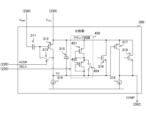
- FIG. 11 is a circuit diagram illustrating a configuration example of a comparator according to a second embodiment of the present technology.
- FIG. 11 is a diagram illustrating an example of a waveform of a reference signal according to a second embodiment of the present technology.
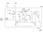
- FIG. 13 is a circuit diagram illustrating a configuration example of a comparator according to a third embodiment of the present technology.
- FIG. 13 is a circuit diagram illustrating a configuration example of a comparator according to a fourth embodiment of the present technology.
- FIG. 13 is a circuit diagram illustrating a configuration example of a comparator according to a fifth embodiment of the present technology.
- FIG. 23 is a circuit diagram illustrating a configuration example of a comparator according to a sixth embodiment of the present technology.
- FIG. 23 is a circuit diagram illustrating a configuration example of a comparator according to a seventh embodiment of the present technology.
- FIG. 23 is a circuit diagram showing another example of a comparator according to the seventh embodiment of the present technology.
- FIG. 23 is a circuit diagram illustrating a configuration example of a comparator according to an eighth embodiment of the present technology.
- FIG. 23 is a circuit diagram showing another example of a comparator according to the eighth embodiment of the present technology.
- FIG. 23 is a circuit diagram illustrating a configuration example of a comparator according to a ninth embodiment of the present technology.
- FIG. 23 is a circuit diagram of a comparator when a connection of a transistor is switched according to a ninth embodiment of the present technology.
- FIG. 23 is a circuit diagram of a comparator when a connection of a transistor is switched according to a ninth embodiment of the present technology.
- FIG. 23 is a circuit diagram showing a configuration example of a comparator according to a tenth embodiment of the present technology.
- FIG. 23 is a circuit diagram showing a configuration example of a comparator according to an eleventh embodiment of the present technology.
- FIG. 29 is a circuit diagram showing a configuration example of a comparator according to a twelfth embodiment of the present technology.
- 23 is a timing chart showing an example of an operation of a solid-state imaging element according to a twelfth embodiment of the present technology.
- 1 is a block diagram showing a schematic configuration example of a vehicle control system;
- FIG. 4 is an explanatory diagram showing an example of an installation position of an imaging unit.
- First embodiment (example of switching clamp voltage) 2.
- Second embodiment (example of changing the slope of the reference signal and switching the clamp voltage) 3.
- Third embodiment (example of changing the connection destination of a switch and switching the clamp voltage) 4.
- Fourth embodiment (example of switching clamp voltage with one-stage diode connection) 5.
- Fifth embodiment (example of switching clamp voltage by changing switch connection destination with one-stage diode connection) 6.
- Sixth embodiment (example of switching clamp voltage in three stages) 7.
- Seventh embodiment (example of switching clamp voltage by changing the total gate width of transistors) 8.
- Eighth embodiment (an example in which clamp voltage is switched by switching circuits connected in parallel) 9.
- Ninth embodiment (example of switching clamp voltage by changing transistor connection configuration) 10.
- Tenth embodiment (example in which a mirror capacitance is added and a clamp voltage is switched) 11.
- Eleventh embodiment (example in which a mirror capacitance and a resistor are added and the clamp voltage is switched) 12.
- Twelfth embodiment (example in which a level shift circuit is added and clamp voltage is switched) 13. Examples of applications to moving objects
- First embodiment [Configuration example of imaging device] 1 is a block diagram showing an example of a configuration of an imaging device 100 according to a first embodiment of the present technology.
- the imaging device 100 is a device for capturing image data, and includes an optical unit 110, a solid-state imaging element 200, and a DSP (Digital Signal Processing) circuit 120.
- the imaging device 100 further includes a display unit 130, an operation unit 140, a bus 150, a frame memory 160, a storage unit 170, and a power supply unit 180.
- the imaging device 100 is assumed to be a camera mounted on a smartphone, an in-vehicle camera, or the like.
- the optical unit 110 collects light from a subject and guides it to the solid-state imaging element 200.
- the solid-state imaging element 200 generates image data by photoelectric conversion.
- the solid-state imaging element 200 supplies the generated image data to the DSP circuit 120 via a signal line 209.
- the DSP circuit 120 performs a predetermined signal processing on the image data. This DSP circuit 120 outputs the processed image data to the frame memory 160 or the like via the bus 150. Note that the DSP circuit 120 is an example of a signal processing circuit as described in the claims.
- the display unit 130 displays image data.
- the display unit 130 may be, for example, a liquid crystal panel or an organic EL (Electro Luminescence) panel.
- the operation unit 140 generates an operation signal in accordance with a user's operation.
- the bus 150 is a common path for the optical unit 110, solid-state image sensor 200, DSP circuit 120, display unit 130, operation unit 140, frame memory 160, storage unit 170, and power supply unit 180 to exchange data with each other.
- the frame memory 160 holds image data.
- the storage unit 170 stores various data such as image data.
- the power supply unit 180 supplies power to the solid-state imaging element 200, the DSP circuit 120, the display unit 130, etc.
- Example of the configuration of a solid-state imaging element is a block diagram showing an example of a configuration of a solid-state imaging device 200 according to the first embodiment of the present technology.
- the solid-state imaging device 200 includes a vertical scanning circuit 210, a timing control unit 220, a digital to analog converter (DAC) 230, a pixel array unit 240, a column signal processing unit 260, a horizontal scanning circuit 270, and an image processing unit 280.
- DAC digital to analog converter
- the pixel array section 240 has a plurality of pixel circuits 250 arranged in a two-dimensional grid.
- a set of pixel circuits 250 arranged in a predetermined horizontal direction will be referred to as a "row,” and a set of pixel circuits 250 arranged vertically in a row will be referred to as a "column.”
- the vertical scanning circuit 210 drives the rows in sequence to output the pixel circuits 250.
- the timing control section 220 controls the operation timing of the vertical scanning circuit 210, the DAC 230, the column signal processing section 260, and the horizontal scanning circuit 270 in synchronization with the vertical synchronization signal VSYNC.
- the vertical synchronization signal VSYNC is a periodic signal of a predetermined frequency (e.g., 60 Hz) that indicates the imaging timing.
- the DAC 230 generates a predetermined reference signal by DA (Digital to Analog) conversion. For example, a sawtooth ramp signal is used as the reference signal.
- DA Digital to Analog
- the DAC 230 supplies the reference signal to the column signal processing unit 260.
- the pixel circuit 250 generates an analog pixel signal through photoelectric conversion and supplies it to the column signal processing unit 260.
- the column signal processing unit 260 performs signal processing such as AD conversion and CDS (Correlated Double Sampling) processing on pixel signals for each column.
- This column signal processing unit 260 supplies image data consisting of processed digital signals to the image processing unit 280 via a signal line 209.
- the horizontal scanning circuit 270 controls the column signal processing unit 260 to output digital signals in sequence.
- the image processing unit 280 performs various image processing operations on the image data and supplies the processed data to the DSP circuit 120.
- the image processing unit 280 also measures the illuminance based on the image data, and sets a higher analog gain value as the illuminance decreases.
- the multi-stage analog gain is divided into, for example, two regions, and the analog gain in the higher region is set to "high gain” and the analog gain in the lower region is set to "low gain.”
- the analog gain on the high gain side is set, and when the illuminance is equal to or greater than the specified value, the analog gain on the low gain side is set.
- the image processing unit 280 supplies gain setting information indicating the analog gain setting contents to the timing control unit 220.
- the processing performed by the image processing unit 280 can be performed by a circuit external to the solid-state imaging device 200 (such as the DSP circuit 120).
- Example of pixel circuit configuration is a circuit diagram showing a configuration example of a pixel circuit 250 according to the first embodiment of the present technology.
- the pixel circuit 250 includes a photoelectric conversion element 251, a transfer transistor 252, a reset transistor 253, a floating diffusion layer 254, an amplification transistor 255, and a selection transistor 256.
- a vertical signal line VSL is wired for each column along the vertical direction.
- the photoelectric conversion element 251 converts incident light into an electric charge and generates an electric charge.
- the transfer transistor 252 transfers the electric charge from the photoelectric conversion element 251 to the floating diffusion layer 254 in accordance with a transfer signal TRG from the vertical scanning circuit 210.
- the reset transistor 253 extracts charge from the floating diffusion layer 254 to initialize it in response to a reset signal RST from the vertical scanning circuit 210.
- the floating diffusion layer 254 accumulates electric charge and generates a voltage according to the amount of electric charge.
- the amplifier transistor 255 amplifies the voltage of the floating diffusion layer 254.
- the selection transistor 256 outputs the amplified voltage signal as a pixel signal to the column signal processing unit 260 via the vertical signal line VSL in accordance with the selection signal SEL from the vertical scanning circuit 210.
- pixel circuit 250 is not limited to the circuit shown in the figure, as long as it can generate a pixel signal through photoelectric conversion.
- Example of the configuration of the column signal processing unit] 4 is a block diagram showing an example of a configuration of the column signal processing unit 260 according to the first embodiment of the present technology.
- an ADC 261 and a latch 263 are arranged for each column.
- N is an integer
- N ADCs 261 and latches 263 are arranged.
- the ADC 261 is a single slope type and includes a comparator 300 and a counter 262.
- the comparator 300 compares a reference signal from the DAC 230 with a pixel signal from a corresponding column.
- the voltage of the reference signal is referred to as a reference voltage V RMP
- the voltage of the pixel signal input via the vertical signal line VSL is referred to as an input voltage V VSL .
- the comparator 300 supplies a comparison result COMP between the reference voltage V RMP and the input voltage V VSL to the counter 262 of the corresponding column.
- the input voltage V VSL when the pixel circuit 250 is initialized is hereinafter referred to as the "reset level”
- the input voltage V VSL when the charge is transferred to the floating diffusion layer 254 is hereinafter referred to as the “signal level”.
- the counter 262 counts the count value over the period until the comparison result COMP is inverted. For example, the counter 262 counts down over the period until the comparison result COMP with the reset level is inverted, and counts up over the period until the comparison result COMP with the signal level is inverted. This realizes CDS processing that finds the difference between the reset level and the signal level.
- the counter 262 then causes the latch 263 to hold a digital signal indicating the count value.
- CDS process is realized by counting up and counting down, this is not a limitation.
- the counter 262 may only count up or count down, and a downstream circuit may execute the CDS process to find the difference.
- the latch 263 holds the digital signal. This latch 263 outputs the held digital signal to the image processing unit 280 according to the control of the horizontal scanning circuit 270.
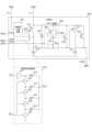
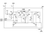
- [Example of comparator configuration] 5 is a circuit diagram showing a configuration example of the comparator 300 according to the first embodiment of the present technology.
- the comparator 300 includes an attenuation rate switching circuit 410, an input transistor 312, an auto-zero switch 313, a current source 314, a band-limiting capacitance 315, and a clamp circuit 450.
- the comparator 300 further includes an n-channel Metal Oxide Semiconductor (nMOS) clamp transistor 316, an output transistor 317, a current source 318, and an nMOS clamp transistor 319.
- nMOS Metal Oxide Semiconductor
- the attenuation rate switching circuit 410 attenuates the reference voltage V RMP by one of a plurality of attenuation rates and supplies it as V RMP ' to the gate of the input transistor 312.
- This attenuation rate switching circuit 410 includes, for example, a buffer 411, switches 412 to 415, and capacitors 416 to 419.
- a reference voltage V RMP is input to an input terminal of a buffer 411.
- a capacitor 416 is inserted between an output terminal of the buffer 411 and an output node of the attenuation rate switching circuit 410.
- One end of each of the capacitors 416 to 419 is commonly connected to the output node of the attenuation rate switching circuit 410.
- Switch 412 opens and closes the path between the input terminals of capacitors 416 and 417.
- Switch 413 opens and closes the path between the input terminals of capacitors 417 and 418.
- Switch 414 opens and closes the path between the input terminals of capacitors 418 and 419.
- Switch 415 opens and closes the path between the input terminal of capacitor 419 and the ground node.
- switches 412 to 415 open and close in accordance with a control signal Gctrl from the timing control section 220.
- the attenuation rate of the reference voltage V RMP increases as the capacitance value connected between the ground node and the output node of the attenuation rate switching circuit 410 increases compared to the capacitance value connected between the output terminal of the buffer 411 and the output node of the attenuation rate switching circuit 410 by opening and closing the switches.
- the slope of V RMP ' supplied to the gate of the input transistor 312 decreases, and the time until the comparison result of the comparator 300 is inverted becomes longer, and the count value of the counter 262 at the subsequent stage becomes larger. This produces the effect of amplifying the pixel signal in the ADC 261.
- This amplification rate of the pixel signal corresponds to the analog gain described above.
- the timing control section 220 increases the attenuation rate of the attenuation rate switching circuit 410 using the control signal Gctrl as the set value of the analog gain indicated by the gain setting information increases, and controls the analog gain to the set value in conjunction with the control of the slope of the reference voltage V RMP .
- the source of the input transistor 312 is connected to the vertical signal line, and the input voltage V VSL is input to the source.
- the reference voltage V RMP ' from the attenuation rate switching circuit 410 is input to the gate of the input transistor 312.
- the input transistor 312 is in the same voltage state as during auto-zero, and outputs a drain voltage Vd according to the input voltage V VSL and the reference voltage V RMP ' from the drain.
- approximately equal means that the changes from the voltage values during the respective auto-zero periods are completely equal, or the difference is within a predetermined tolerance.
- a pMOS transistor is used as the input transistor 312.
- the auto-zero switch 313 shorts the gate and drain of the input transistor 312 in accordance with a control signal AZSW from the timing control unit 220.
- Current source 314 is inserted between the drain of input transistor 312 and the ground node. This current source 314 supplies a constant current.
- Current source 314 is realized by an nMOS (n-channel MOS) transistor or the like.
- the band-limiting capacitance 315 is inserted between the source and drain of the input transistor 312.
- the clamp circuit 450 limits the lower limit of the drain voltage Vd by a voltage selected from a plurality of different clamp voltages in accordance with a control signal SELC.
- the control signal SELC is supplied, for example, by the timing control unit 220.
- the clamp circuit 450 includes pMOS clamp transistors 451 and 452 and a switch 454.
- the pMOS clamp transistors 451 and 452 are connected in series between the source and drain of the input transistor 312.
- the pMOS clamp transistor 451 is on the source side of the input transistor 312.
- the gate and drain of the pMOS clamp transistor 451 are connected, and the gate and drain of the pMOS clamp transistor 452 are also connected. In other words, these transistors are individually diode-connected.
- pMOS clamp transistor 451 is an example of a first clamp transistor as described in the claims
- pMOS clamp transistor 452 is an example of a second clamp transistor as described in the claims.
- Switch 454 shorts the source and drain of pMOS clamp transistor 451 according to the control signal SELC.
- the nMOS clamp transistor 316 limits the lower limit of the drain voltage Vd. This nMOS clamp transistor 316 is inserted between the source and drain of the input transistor 312, and a predetermined bias voltage is applied to the gate.
- the source of the output transistor 317 is connected to the vertical signal line VSL, and an input voltage V VSL is input to the source.
- the gate of the output transistor 317 is connected to the drain of the input transistor 312, and a drain voltage Vd is input to the gate.
- a pMOS transistor is used as the output transistor 317. It is preferable that the back gate and the source of the output transistor 317 are short-circuited.
- the output transistor 317 outputs from its drain a signal indicating whether or not the difference between the input voltage V VSL input to its source and the drain voltage Vd input to its gate exceeds a predetermined threshold voltage as a comparison result COMP.
- This comparison result COMP is supplied to the counter 262.
- the input transistor 312 supplies its drain-source voltage to the gate-source of the output transistor 317, so the comparison result COMP can be inverted at the ideal timing when the input voltage and the reference voltage match. This reduces nonlinearity caused by errors in the inversion timing, and improves the image quality of the image data.
- Current source 318 is inserted between the drain of output transistor 317 and the ground node, and supplies a constant current.
- Current source 318 is realized by an nMOS transistor or the like.
- the nMOS clamp transistor 319 limits the lower limit of the comparison result COMP. This nMOS clamp transistor 319 is inserted between the source and drain of the output transistor 317, and a predetermined bias voltage is applied to the gate.
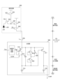
- FIG. 6 is a diagram for explaining a dynamic range and an output amplitude when the analog gain is a low gain in the first embodiment of the present technology.
- the sum of the drain-source voltages when the amplification transistor 255 and the selection transistor 256 in the pixel circuit 250 are in the on state is defined as the “pixel operating voltage.”
- the upper limit of the input voltage V VSL from the vertical signal line 259 is a value lower than the power supply voltage VDD by the pixel operating voltage.
- the amplitude of the drain voltage when the input transistor 312 is in an on state is defined as the "first-stage output amplitude.”
- the voltage between the allowable lower limit voltage of the connection node of the input transistor 312 and the current source 314 and the potential VSS of the ground node is defined as the “current source operating voltage.”
- the lower limit of the input voltage V VSL which is the voltage of the pixel signal, is the sum of the first-stage output amplitude and the current source operating voltage. The voltage difference between the upper and lower limits of this pixel signal is called the "VSL dynamic range.”
- the timing control unit 220 closes the switch 454 as shown in the figure. This disables the pMOS clamp transistor 451, and the pMOS clamp transistor becomes a single stage.
- the pMOS clamp transistor is a single stage, the first stage output amplitude becomes smaller compared to when the pMOS clamp transistor is a two stage stage.
- the VSL dynamic range becomes wider accordingly.
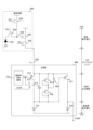
- FIG. 7 is a diagram illustrating the dynamic range and output amplitude when the analog gain is high in the first embodiment of the present technology.
- the timing control unit 220 opens the switch 454 as shown in the figure. This results in two stages of serially connected pMOS clamp transistors. When two stages of pMOS clamp transistors are used, the first stage output amplitude becomes larger compared to when there is a single stage of pMOS clamp transistors. This narrows the VSL dynamic range accordingly.
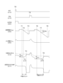
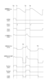
- FIG. 8 is a timing chart showing an example of the operation of the solid-state imaging element 200 when the analog gain is low in the first embodiment of the present technology.
- the vertical scanning circuit 210 supplies a high-level reset signal RST to the pixel to be read. Also, from timing T0 through a certain period, the timing control unit 220 supplies a high-level control signal AZSW to turn on the auto-zero switch 313.
- the input voltage V VSL becomes a reset level by the reset signal RST, and this level is also called the P-phase level.
- the first stage output Vd drops to the clamp voltage, and the potential difference between the voltage at the time of the drop and V VSL (reset level) corresponds to the first stage output amplitude ⁇ V L described above.
- the dotted curve adjacent to the locus of Vd indicates the locus of V VSL .
- the reference voltage V RMP gradually drops over the P-phase count period from timing T1 to T4.
- the first stage output Vd starts to invert, and at the following timing T3, the second stage output COMP is inverted.
- a counter 262 (not shown) counts over the period from timing T1 to T3, and obtains the count value as a reset level (P-phase level).
- the time from timing T2 to T3 is defined as an inversion delay Td L.
- the vertical scanning circuit 210 supplies a high-level transfer signal TRG to the pixel to be read.
- This transfer signal TRG causes the input voltage V VSL to drop to a signal level, which is also called the D-phase level.
- the first-stage output Vd drops to the clamp voltage, and the potential difference between the voltage at the time of this drop and V VSL (signal level) corresponds to the first-stage output amplitude ⁇ V L described above.
- the reference voltage V RMP is initialized once and gradually drops over the D-phase count period from timing T6 to T9.
- the first-stage output Vd starts to invert, and at timing T8 after an inversion delay ⁇ Td L , the second-stage output COMP is inverted.
- the counter 262 counts and obtains the count value as the signal level (D-phase level). The difference between the reset level and the signal level is output as a digital value representing the net signal level ⁇ SIG.
- FIG. 9 is a timing chart showing an example of the operation of the solid-state imaging element 200 when the analog gain is high in the first embodiment of the present technology.
- the first stage output amplitude ⁇ VH is larger than the first stage output amplitude ⁇ VL in the case of low gain.
- the dotted curve adjacent to the locus of Vd indicates the locus of V VSL .
- the inversion delay TdH in the case of high gain becomes longer than the inversion delay ⁇ TdL in the case of low gain.
- the inversion delay ⁇ TdH is long, the time for the noise of the first stage output to be averaged by the band limiting capacitance 315 until inversion becomes long, and the noise becomes smaller accordingly. In terms of frequency characteristics, this corresponds to a smaller noise band width (NBW).
- NBW noise band width
- the noise of the DAC 230 and the like is also reduced, and the cross noise is also improved.
- the timing control section 220 controls the clamp circuit 450 to set the pMOS clamp transistor to one stage. This makes the clamp voltage higher than in the case of two stages, and the first stage output amplitude is accordingly smaller. The dynamic range is wider because the first stage output amplitude is smaller. Also, the inversion delay is smaller and the noise is larger than in the case of two stages. However, since quantization error is dominant when low gain is used, large noise does not cause any problems.
- the timing control section 220 controls the clamp circuit 450 to set the pMOS clamp transistor to two stages. This results in a lower clamp voltage than in the case of one stage, and the first stage output amplitude becomes larger accordingly.
- the dynamic range becomes narrower as the first stage output amplitude becomes larger.
- the inversion delay becomes larger than in the case of one stage, which reduces noise.
- a circuit with a fixed number of stages of pMOS clamp transistors is considered as a comparative example.
- this comparative example it is difficult to increase the first-stage output amplitude in order to further reduce noise. Narrowing the dynamic range makes it possible to increase the first-stage output amplitude accordingly, but this is not desirable as it leads to a decrease in image quality, particularly in the case of low gain.
- lowering the minimum allowable drain voltage of the current source makes it possible to increase the first-stage output amplitude, but this increases the mutual conductance and the noise converted into VSL, making it impossible to achieve the goal of noise reduction.
- the solid-state imaging element 200 switches between two analog gain levels, but can also switch between three or more levels as described below.
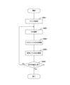
- FIG. 11 is a flowchart showing an example of the operation of the solid-state imaging device 200 in the first embodiment of the present technology. This operation is started, for example, when a specific application for capturing image data is executed.
- the solid-state imaging device 200 sets an analog gain according to the illuminance (step S901). At this time, the number of stages of the pMOS clamp transistor is controlled according to the analog gain.
- the solid-state imaging element 200 selects the row to be read out after exposure (step S902). Then, the solid-state imaging element 200 performs A/D conversion on the reset level of the selected row (step S903) and A/D conversion on the signal level (step S904). The solid-state imaging element 200 determines whether or not reading out of all rows has been completed (step S905).
- step S905 If reading out of all rows has not been completed (step S905: No), the solid-state imaging element 200 repeats steps S902 and onwards. On the other hand, if reading out of all rows has been completed (step S905: Yes), the solid-state imaging element 200 ends the operation for capturing image data. When capturing multiple pieces of image data consecutively, steps S901 to S905 are repeatedly executed in synchronization with the vertical synchronization signal VSYNC.
- the clamp circuit 450 limits the lower limit of the drain voltage Vd using a clamp voltage that corresponds to the analog gain, making it possible to reduce noise while maintaining the dynamic range.
- the analog gain is switched by changing the attenuation rate for the reference voltage V RMP , but the analog gain can also be switched by changing only the slope of the reference voltage V RMP .
- the solid-state imaging device 200 of the second embodiment differs from the first embodiment in that it does not have an attenuation rate switching circuit 410.
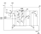
- FIG. 12 is a circuit diagram showing an example of the configuration of a comparator 300 in a second embodiment of the present technology.
- the comparator 300 in the second embodiment differs from the first embodiment in that the attenuation rate switching circuit 410 is omitted and a capacitor 311 is provided instead.
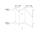
- FIG. 13 is a diagram showing an example of a waveform of a reference signal in the second embodiment of the present technology.
- "a” is a diagram showing an example of a waveform of a reference signal when the analog gain is controlled to a low gain.
- "b” is a diagram showing an example of a waveform of a reference signal when the analog gain is controlled to a high gain.
- the reference voltage V RMP of the reference signal gradually decreases over the P-phase count period. Also, in the D-phase count period, the reference signal RMP gradually decreases, and the amplitude of the reference signal V RMP is larger than that of the AD conversion period of the reset level.
- the amplitude of the reference signal RMP when controlling to a low gain, the amplitude of the reference signal RMP is greater than that in the case of a high gain. Also, as shown in FIG. 1B, when controlling to a high gain, the amplitude of the reference signal RMP is smaller than that in the case of a low gain.
- the timing control unit 220 controls the DAC 230 according to the gain setting information, and switches the analog gain by changing the slope of the reference signal.
- the analog gain can also be switched by a method other than the attenuation rate switching circuit 410 or changing the slope of the reference signal.
- a variable gain amplifier can be inserted between the comparator 300 and the pixel circuit 250, and the timing control unit 220 or the like can switch the gain.
- the timing control unit 220 controls the DAC 230 to change the analog gain based only on the slope of the reference signal, so that the attenuation rate switching circuit 410 can be eliminated.
- the switch 454 in the clamp circuit 450 shorts the source and drain of the upper pMOS clamp transistor 451, but this is not limited to the circuit configuration.
- the solid-state imaging device 200 of the third embodiment differs from the second embodiment in that the switch 454 shorts the source and drain of the lower pMOS clamp transistor 452.
- FIG. 14 is a circuit diagram showing an example of a configuration of a comparator 300 in a third embodiment of the present technology.
- the comparator 300 in this third embodiment differs from the second embodiment in that a switch 454 shorts the source and drain of the lower pMOS clamp transistor 452.
- one end of the switch 454 is connected to the output of the first-stage input transistor 312.
- the control line that transmits the control signal SELC to the switch 454 will become an interference path for other columns.
- the control line may become an interference path, thereby canceling out interference from other factors, and in that case, noise can be suppressed.
- the attenuation rate switching circuit 410 of the first embodiment can also be provided in the third embodiment.
- the switch 454 shorts the source and drain of the lower pMOS clamp transistor 452, thereby disabling the pMOS clamp transistor 452.
- the pMOS clamp transistors 451 and 452 are each individually diode-connected, but their gates can also be commonly connected to the drain of the pMOS clamp transistor 452.
- the solid-state imaging device 200 in the fourth embodiment differs from the second embodiment in that the gates of the pMOS clamp transistors 451 and 452 are commonly connected to the drain of the pMOS clamp transistor 452.
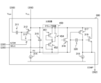
- FIG. 15 is a circuit diagram showing an example of the configuration of a comparator 300 in a fourth embodiment of the present technology.
- the comparator 300 in this fourth embodiment differs from the second embodiment in that the gates of the pMOS clamp transistors 451 and 452 are commonly connected to the drain of the pMOS clamp transistor 452.
- the second embodiment has two stages of diode connections
- the fourth embodiment has one stage of diode connections. By using one stage of diode connections, it is possible to reduce the output amplitude of the first stage input transistor 312 and the PVT (Process, Voltage, Temperature) fluctuations of the NBW compared to the two-stage case.
- PVT Process, Voltage, Temperature
- the attenuation rate switching circuit 410 of the first embodiment can also be provided in the fourth embodiment.
- the diode connection is in one stage, it is possible to reduce the PVT fluctuation of the output amplitude and NBW of the first stage.
- the solid-state imaging device 200 of the fifth embodiment differs from the fourth embodiment in that the switch 454 shorts the source and drain of the lower pMOS clamp transistor 452.
- FIG. 16 is a circuit diagram showing an example of a configuration of a comparator 300 in a fifth embodiment of the present technology.
- the comparator 300 in the fifth embodiment differs from the fourth embodiment in that a switch 454 shorts the source and drain of the lower pMOS clamp transistor 452.
- the attenuation rate switching circuit 410 of the first embodiment can also be provided in the fifth embodiment.
- the switch 454 shorts the source and drain of the lower pMOS clamp transistor 452, thereby disabling the pMOS clamp transistor 452.
- the diode connection is in one stage and the pMOS clamp transistor is in two stages, but this configuration does not allow the clamp voltage to be switched in three stages.
- the solid-state imaging device 200 in the sixth embodiment differs from the fourth embodiment in that the pMOS clamp transistor is in three stages.
- FIG. 17 is a circuit diagram showing an example of a configuration of a comparator 300 in a sixth embodiment of the present technology.
- the comparator 300 in the sixth embodiment differs from the fourth embodiment in that it further includes a pMOS clamp transistor 453 and a switch 455.
- the pMOS clamp transistor 453 is inserted between the drain of the pMOS clamp transistor 452 and the drain of the input transistor 312. In addition, the gates of the pMOS clamp transistors 451, 452, and 453 are commonly connected to the drain of the pMOS clamp transistor 453.
- Switches 454 and 455 short-circuit the sources and drains of two of the three pMOS clamp transistors according to control signals SELC1 and SELC2. For example, switch 454 shorts the source and drain of pMOS clamp transistor 451 according to control signal SELC1, and switch 455 shorts the source and drain of pMOS clamp transistor 452 according to control signal SELC2.
- the timing control section 220 controls the analog gain in three regions. In this case, the timing control section 220 increases the number of pMOS clamp transistor stages as the analog gain increases using the control signals SELC1 and SELC2.
- the number of analog gain stages can be four or more, and pMOS clamp transistors and switches can be added according to the number of stages.
- the sixth embodiment can also be provided with the attenuation rate switching circuit 410 of the first embodiment.
- the diode connection can also be three stages instead of one stage.
- the pMOS clamp transistors are arranged in three stages, so the timing control unit 220 controls the analog gain by dividing it into three regions. By dividing the regions into smaller regions, it is possible to reduce noise steps at the boundaries between the regions.
- the pMOS clamp transistors 451 and 452 are connected in series, but the present invention is not limited to this connection.
- the solid-state imaging device 200 in the seventh embodiment differs from the second embodiment in that the pMOS clamp transistors 451 and 452 are connected in parallel.
- FIG. 18 is a circuit diagram showing an example of a configuration of a comparator 300 in a seventh embodiment of the present technology.
- the comparator 300 in the seventh embodiment differs from the second embodiment in that pMOS clamp transistors 451 and 452 are connected in parallel by a switch 454.
- the sources of pMOS clamp transistors 451 and 452 are commonly connected to the source of input transistor 312.
- the drain of pMOS clamp transistor 452 is connected to the drain of input transistor 312.
- Switch 454 opens and closes the path between the drain of pMOS clamp transistor 451 and the drain of input transistor 312 in accordance with control signal SELC. Also, by providing switch 455 that is controlled exclusively with switch 454 and closing it when switch 454 is open, unexpected operation caused by the drain and gate voltages of pMOS clamp transistor 451 becoming floating may be avoided.
- timing control section 220 controls switch 454 to a closed state and switch 455 to an open state, and when high gain is set, controls switch 454 to an open state and switch 455 to a closed state.
- the sum of the gate lengths of the pMOS clamp transistors is controlled, whereas in the seventh embodiment, the sum of the gate widths is controlled.
- the gates of pMOS clamp transistors 451 and 452 can also be commonly connected to the drain of input transistor 312.
- the seventh embodiment can also be provided with the attenuation rate switching circuit 410 of the first embodiment.
- the number of pMOS clamp transistors can also be set to three or more, allowing the analog gain to be switched between three or more stages.
- the switch 454 connects the pMOS clamp transistors 451 and 452 in parallel, making it possible to control the sum of the gate widths of these transistors.
- the switch 454 shorts the source and drain of one of the pMOS clamp transistors 451 and 452, but this is not limiting.
- the solid-state imaging device 200 in the eighth embodiment differs from the second embodiment in that the number of stages is switched without shorting the source and drain of one of the pMOS clamp transistors connected in series.
- FIG. 20 is a circuit diagram showing an example of the configuration of a comparator 300 in an eighth embodiment of the present technology.
- the comparator 300 in the eighth embodiment differs from the second embodiment in that it further includes a pMOS clamp transistor 453 and switches 455, 456, and 457.
- the pMOS clamp transistors 451 and 452 are connected in series. These transistors are also individually diode-connected.
- the switch 454 connects the pMOS clamp transistor 453 in parallel to the input transistor 312 according to the control signal SELC.
- the source of the pMOS clamp transistor 453 is connected to the source of the input transistor 312, and the switch 454 connects the drain of the pMOS clamp transistor 453 to the drain of the input transistor 312 during low gain.
- a switch 456 that is controlled exclusively with the switch 454 may be provided and closed when the switch 454 is open, thereby preventing unexpected operation caused by the drain and gate voltages of the pMOS clamp transistor 453 becoming floating.
- switch 455 is controlled exclusively with switch 454.
- switch 455 connects the circuit consisting of pMOS clamp transistors 451 and 452 to input transistor 312 in parallel.
- the source of pMOS clamp transistor 451 is connected to the source of input transistor 312, and switch 455 connects the drain of pMOS clamp transistor 452 to the drain of input transistor 312 during high gain.
- switch 457 which is controlled exclusively with switch 455, may be provided and closed when switch 455 is open, thereby avoiding unexpected operation caused by the drain and gate voltages of pMOS clamp transistor 452 becoming floating.
- connection of the gate of pMOS clamp transistor 451 can also be changed, as shown in FIG. 21.
- the gates of pMOS clamp transistors 451 and 452 are commonly connected to the drain of pMOS clamp transistor 452.
- the eighth embodiment can also be provided with the attenuation rate switching circuit 410 of the first embodiment.
- Three or more pMOS clamp transistors and switches connected in series can also be added to switch the analog gain in three or more stages.
- the three-stage diode connection can also be reduced to one stage.
- the pMOS clamp transistors 451 and 452 are connected in series, but the connection is not limited to this.
- the solid-state imaging device 200 in the seventh embodiment differs from the second embodiment in that the connection can be switched between series and parallel.
- FIG. 22 is a circuit diagram showing an example of the configuration of the comparator 300 in the ninth embodiment of the present technology.
- a is a circuit diagram showing an example of the state of the comparator 300 in the case of low gain
- b in the figure is a circuit diagram showing the connection form of the pMOS clamp transistors 451 and 452 in the case of low gain.
- the comparator 300 in the ninth embodiment differs from the second embodiment in that it further includes switches 455 and 456.
- the pMOS clamp transistors 451 and 452 are connected in series, and their gates are commonly connected to the drain of the pMOS clamp transistor 452.
- the drain of the pMOS clamp transistor 452 is also connected to the drain of the input transistor 312.
- Switch 454 opens and closes the path between the source of pMOS clamp transistor 451 and the source of input transistor 312 according to the control signal SELC.
- Switch 455 opens and closes the path between the source of pMOS clamp transistor 451 and the drain of input transistor 312 according to the control signal SELC.
- Switch 456 opens and closes the path between the connection node of pMOS clamp transistors 451 and 452 and the source of input transistor 312 according to the control signal SELC.
- Switch 454 and switches 455 and 456 are controlled exclusively. In the case of low gain, the timing control unit 220 opens switch 454 and closes switches 455 and 456, as shown in FIG. a.
- pMOS clamp transistors 451 and 452 can be connected in parallel as illustrated in FIG. 1b.
- the switches are omitted in FIG. 1b. If the gate length and gate width of each pMOS clamp transistor are L and W, the aspect ratio when connected in parallel is (2W)/L.
- the timing control unit 220 closes switch 454 and opens switches 455 and 456.
- pMOS clamp transistors 451 and 452 can be connected in series as illustrated in FIG. 1b.
- the switches are omitted in FIG. 1b.
- the aspect ratio when connected in series is W/(2L).
- the clamp voltage can be switched and the NBW can be reduced at high gain.
- the attenuation rate switching circuit 410 of the first embodiment can also be provided in the ninth embodiment.
- the band-limiting capacitance 315 is inserted between the source and drain of the input transistor 312, but it may be difficult to sufficiently reduce the NBW with only this capacitance.
- the solid-state imaging device 200 in the tenth embodiment differs from the second embodiment in that a mirror capacitance is inserted between the gate and drain of the output transistor 317.
- FIG. 24 is a circuit diagram showing an example of the configuration of a comparator 300 in a tenth embodiment of the present technology.
- the comparator 300 in this tenth embodiment differs from the second embodiment in that it further includes a mirror capacitance 320.
- This mirror capacitance 320 is inserted between the gate and drain of the output transistor 317. By placing the mirror capacitance 320 in this position, the capacitance value appears larger by the amount of the gain of the second stage, and the NBW can be made smaller.
- the attenuation rate switching circuit 410 of the first embodiment can also be provided in the tenth embodiment. Also, each of the third to ninth embodiments can be applied to the tenth embodiment.
- the mirror capacitance 320 is inserted between the gate and drain of the output transistor 317, thereby making it possible to further reduce the NBW.
- the mirror capacitance 320 is inserted between the gate and drain of the output transistor 317, but the addition of the mirror capacitance 320 may cause the circuit to become unstable.
- the solid-state imaging device 200 in the eleventh embodiment differs from the tenth embodiment in that a resistor is added.
- FIG. 25 is a circuit diagram showing an example configuration of a comparator 300 in an eleventh embodiment of the present technology.
- the comparator 300 in the eleventh embodiment differs from the tenth embodiment in that it further includes a resistor 321.
- the resistor 321 is inserted between one end of the mirror capacitance 320 and the gate of the output transistor 317. The addition of the resistor 321 can stabilize the circuit.
- the attenuation rate switching circuit 410 of the first embodiment can also be provided in the eleventh embodiment. Also, each of the third to ninth embodiments can be applied to the eleventh embodiment.
- the resistor 321 is inserted between one end of the mirror capacitance 320 and the gate of the output transistor 317, thereby stabilizing the circuit.
- Twelfth embodiment In the first embodiment described above, the output of the second-stage output transistor 317 is directly output as the comparison result COMP, but the voltage range of this comparison result signal may be insufficient.
- the solid-state imaging device 200 in the twelfth embodiment differs from the first embodiment in that the voltage range of the comparison result signal is expanded.
- FIG. 26 is a circuit diagram showing an example of a configuration of a comparator 300 in a twelfth embodiment of the present technology.
- the comparator 300 in the twelfth embodiment differs from the first embodiment in that it further includes a switch 322, a switch 323, an nMOS clamp transistor 324, a level shift circuit 460, and a NAND (negative AND) gate 325.
- the switch 322 opens and closes the path between the input transistor 312 and the current source 314 in accordance with the control signal XPAC1 from the timing control unit 220. This switch 322 transitions to a closed state when the control signal XPAC1 is at a high level.
- Switch 323 opens and closes the path between the source and drain of output transistor 317 in accordance with control signal PAC2 from timing control unit 220. This switch 323 transitions to a closed state when control signal PAC2 is at a high level.
- the nMOS clamp transistor 324 limits the lower limit of the second stage output. This nMOS clamp transistor 324 is diode-connected and inserted between the source and drain of the output transistor 317. This nMOS clamp transistor 324 can prevent the output of the second stage from fluctuating too much and causing interference with other columns.
- the level shift circuit 460 outputs one of a pair of shift potentials, the difference between which is greater than the high and low levels of the output signal of the second-stage output transistor 317, to the NAND gate 325.
- This level shift circuit 460 includes switches 461 and 464, an nMOS transistor 462, and a pMOS transistor 463.
- the switch 461 opens and closes the path between the power supply voltage VDDH and the drain of the nMOS transistor 462 in accordance with the control signal PreChg1 from the timing control unit 220.
- the power supply voltage VDDH is a voltage higher than the upper limit of the output amplitude of the output transistor 317 (in other words, the lower limit of the VSL dynamic range).
- the switch 461 transitions to a closed state when the control signal PreChg1 is at a high level.
- the switch 461 may be configured with a pMOS transistor. In that case, the switch transitions to a closed state when the control signal PreChg1 is at a low level.
- nMOS transistor 462 The gate of nMOS transistor 462 is connected to the source of output transistor 317, and the source of nMOS transistor 462 is connected to the drain of output transistor 317.
- the gate of pMOS transistor 463 is connected to the connection node between switch 461 and nMOS transistor 462, and the source is connected to power supply voltage VDDH.
- the switch 464 opens and closes the path between the drain of the pMOS transistor 463 and the ground node in accordance with the control signal PreChg2 from the timing control unit 220. Furthermore, the switch 464 transitions to a closed state when the control signal PreChg2 is at a high level. One of a pair of shift potentials is output from the connection node between the pMOS transistor 463 and the switch 464.
- the NAND gate 325 outputs the negative logical product of the enable signal EN from the timing control unit 220 or the like and the output of the level shift circuit 460 as the comparison result COMP to the counter 262.
- the enable signal EN is at a high level, the output of the level shift circuit 460 is inverted and output as the comparison result COMP.
- the level shift circuit 460 expands the voltage range of the comparison result signal, making it possible to suppress malfunctions in downstream logic circuits, etc.
- FIG. 27 is a timing chart showing an example of the operation of the solid-state imaging device 200 in the twelfth embodiment of the present technology. From timing T0, the timing control unit 220 sets the control signal AZSW to a high level for a certain period of time.
- the timing control unit 220 also sets the control signal XPAC1 to a low level over the pulse period from timing T1. This makes it possible to speed up the rise of the first stage output voltage when the reference signal starts to rise.
- the timing control unit 220 also keeps the control signal PAC2 at a high level for the period up to timing T1. This allows the second-stage output level to be raised to VSL in advance, speeding up the initialization of the second-stage output. At the same time, the second-stage output transistor 317 is disabled when not in use, reducing the risk of the circuit becoming unstable.
- the timing control unit 220 also sets the control signals PreChg1 and PreChg2 to a high level between immediately after timing T0 and immediately before timing T1.
- the comparison result COMP is inverted immediately after timing T2.
- the timing control unit 220 also sets the control signal XPAC1 to a low level from timing T4 over the pulse period.
- the timing control unit 220 also sets the control signal XPAC2 to a high level over the period from timing T3 to T4.
- the timing control unit 220 also sets the control signals PreChg1 and PreChg2 to a high level between immediately after timing T3 and immediately before timing T4.
- the comparison result COMP is inverted immediately after timing T5. If the switch 461 is configured with a pMOS transistor, the control signal PreChg1 is inverted between a high level and a low level.
- each of the second to eleventh embodiments can be applied to the twelfth embodiment.
- the level shift circuit 460 expands the voltage range of the comparison result signal, making it possible to suppress malfunctions of downstream logic circuits, etc.
- the technology according to the present disclosure can be applied to various products.
- the technology according to the present disclosure may be realized as a device mounted on any type of moving body such as an automobile, an electric vehicle, a hybrid electric vehicle, a motorcycle, a bicycle, a personal mobility device, an airplane, a drone, a ship, or a robot.
- FIG. 28 is a block diagram showing a schematic configuration example of a vehicle control system, which is an example of a mobile object control system to which the technology disclosed herein can be applied.
- the vehicle control system 12000 includes a plurality of electronic control units connected via a communication network 12001.
- the vehicle control system 12000 includes a drive system control unit 12010, a body system control unit 12020, an outside vehicle information detection unit 12030, an inside vehicle information detection unit 12040, and an integrated control unit 12050.
- Also shown as functional components of the integrated control unit 12050 are a microcomputer 12051, an audio/video output unit 12052, and an in-vehicle network I/F (interface) 12053.
- the drive system control unit 12010 controls the operation of devices related to the drive system of the vehicle according to various programs.
- the drive system control unit 12010 functions as a control device for a drive force generating device for generating the drive force of the vehicle, such as an internal combustion engine or a drive motor, a drive force transmission mechanism for transmitting the drive force to the wheels, a steering mechanism for adjusting the steering angle of the vehicle, and a braking device for generating a braking force for the vehicle.
- the body system control unit 12020 controls the operation of various devices installed in the vehicle body according to various programs.
- the body system control unit 12020 functions as a control device for a keyless entry system, a smart key system, a power window device, or various lamps such as headlamps, tail lamps, brake lamps, turn signals, and fog lamps.
- radio waves or signals from various switches transmitted from a portable device that replaces a key can be input to the body system control unit 12020.
- the body system control unit 12020 accepts the input of these radio waves or signals and controls the vehicle's door lock device, power window device, lamps, etc.
- the outside-vehicle information detection unit 12030 detects information outside the vehicle equipped with the vehicle control system 12000.
- the image capturing unit 12031 is connected to the outside-vehicle information detection unit 12030.
- the outside-vehicle information detection unit 12030 causes the image capturing unit 12031 to capture images outside the vehicle and receives the captured images.
- the outside-vehicle information detection unit 12030 may perform object detection processing or distance detection processing for people, cars, obstacles, signs, or characters on the road surface based on the received images.
- the imaging unit 12031 is an optical sensor that receives light and outputs an electrical signal according to the amount of light received.
- the imaging unit 12031 can output the electrical signal as an image, or as distance measurement information.
- the light received by the imaging unit 12031 may be visible light, or may be invisible light such as infrared light.
- the in-vehicle information detection unit 12040 detects information inside the vehicle.
- a driver state detection unit 12041 that detects the state of the driver is connected.
- the driver state detection unit 12041 includes, for example, a camera that captures an image of the driver, and the in-vehicle information detection unit 12040 may calculate the driver's degree of fatigue or concentration based on the detection information input from the driver state detection unit 12041, or may determine whether the driver is dozing off.
- the microcomputer 12051 can calculate control target values for the driving force generating device, steering mechanism, or braking device based on information inside and outside the vehicle acquired by the outside vehicle information detection unit 12030 or the inside vehicle information detection unit 12040, and output control commands to the drive system control unit 12010.
- the microcomputer 12051 can perform cooperative control aimed at realizing the functions of an ADAS (Advanced Driver Assistance System), including vehicle collision avoidance or impact mitigation, following driving based on the distance between vehicles, maintaining vehicle speed, vehicle collision warning, or vehicle lane departure warning.
- ADAS Advanced Driver Assistance System
- the microcomputer 12051 can also control the driving force generating device, steering mechanism, braking device, etc. based on information about the surroundings of the vehicle acquired by the outside vehicle information detection unit 12030 or the inside vehicle information detection unit 12040, thereby performing cooperative control aimed at automatic driving, which allows the vehicle to travel autonomously without relying on the driver's operation.
- the microcomputer 12051 can also output control commands to the body system control unit 12020 based on information outside the vehicle acquired by the outside-vehicle information detection unit 12030. For example, the microcomputer 12051 can control the headlamps according to the position of a preceding vehicle or an oncoming vehicle detected by the outside-vehicle information detection unit 12030, and perform cooperative control aimed at preventing glare, such as switching high beams to low beams.
- the audio/image output unit 12052 transmits at least one output signal of audio and image to an output device capable of visually or audibly notifying the occupants of the vehicle or the outside of the vehicle of information.
- an audio speaker 12061, a display unit 12062, and an instrument panel 12063 are exemplified as output devices.
- the display unit 12062 may include, for example, at least one of an on-board display and a head-up display.
- FIG. 29 shows an example of the installation position of the imaging unit 12031.
- the imaging unit 12031 includes imaging units 12101, 12102, 12103, 12104, and 12105.
- the imaging units 12101, 12102, 12103, 12104, and 12105 are provided, for example, at the front nose, side mirrors, rear bumper, back door, and upper part of the windshield inside the vehicle cabin of the vehicle 12100.
- the imaging unit 12101 provided at the front nose and the imaging unit 12105 provided at the upper part of the windshield inside the vehicle cabin mainly acquire images of the front of the vehicle 12100.
- the imaging units 12102 and 12103 provided at the side mirrors mainly acquire images of the sides of the vehicle 12100.
- the imaging unit 12104 provided at the rear bumper or back door mainly acquires images of the rear of the vehicle 12100.
- the imaging unit 12105 provided at the upper part of the windshield inside the vehicle cabin is mainly used to detect leading vehicles, pedestrians, obstacles, traffic lights, traffic signs, lanes, etc.
- FIG. 29 shows an example of the imaging ranges of the imaging units 12101 to 12104.
- Imaging range 12111 indicates the imaging range of the imaging unit 12101 provided on the front nose
- imaging ranges 12112 and 12113 indicate the imaging ranges of the imaging units 12102 and 12103 provided on the side mirrors, respectively
- imaging range 12114 indicates the imaging range of the imaging unit 12104 provided on the rear bumper or back door.
- an overhead image of the vehicle 12100 viewed from above is obtained by superimposing the image data captured by the imaging units 12101 to 12104.
- At least one of the imaging units 12101 to 12104 may have a function of acquiring distance information.
- at least one of the imaging units 12101 to 12104 may be a stereo camera consisting of multiple imaging elements, or an imaging element having pixels for detecting phase differences.
- the microcomputer 12051 can obtain the distance to each solid object within the imaging ranges 12111 to 12114 and the change in this distance over time (relative speed with respect to the vehicle 12100) based on the distance information obtained from the imaging units 12101 to 12104, and can extract as a preceding vehicle, in particular, the closest solid object on the path of the vehicle 12100 that is traveling in approximately the same direction as the vehicle 12100 at a predetermined speed (e.g., 0 km/h or faster). Furthermore, the microcomputer 12051 can set the inter-vehicle distance that should be maintained in advance in front of the preceding vehicle, and perform automatic braking control (including follow-up stop control) and automatic acceleration control (including follow-up start control). In this way, cooperative control can be performed for the purpose of automatic driving, which runs autonomously without relying on the driver's operation.
- automatic braking control including follow-up stop control
- automatic acceleration control including follow-up start control
- the microcomputer 12051 classifies and extracts three-dimensional object data on three-dimensional objects, such as two-wheeled vehicles, ordinary vehicles, large vehicles, pedestrians, utility poles, and other three-dimensional objects, based on the distance information obtained from the imaging units 12101 to 12104, and can use the data to automatically avoid obstacles.
- the microcomputer 12051 distinguishes obstacles around the vehicle 12100 into obstacles that are visible to the driver of the vehicle 12100 and obstacles that are difficult to see.
- the microcomputer 12051 determines the collision risk, which indicates the risk of collision with each obstacle, and when the collision risk is equal to or exceeds a set value and there is a possibility of a collision, it can provide driving assistance for collision avoidance by outputting an alarm to the driver via the audio speaker 12061 or the display unit 12062, or by forcibly decelerating or steering the vehicle to avoid a collision via the drive system control unit 12010.
- At least one of the imaging units 12101 to 12104 may be an infrared camera that detects infrared rays.
- the microcomputer 12051 can recognize a pedestrian by determining whether or not a pedestrian is present in the captured image of the imaging units 12101 to 12104. The recognition of such a pedestrian is performed, for example, by a procedure of extracting feature points in the captured image of the imaging units 12101 to 12104 as infrared cameras, and a procedure of performing pattern matching processing on a series of feature points that indicate the contour of an object to determine whether or not it is a pedestrian.
- the audio/image output unit 12052 controls the display unit 12062 to superimpose a rectangular contour line for emphasis on the recognized pedestrian.
- the audio/image output unit 12052 may also control the display unit 12062 to display an icon or the like indicating a pedestrian at a desired position.
- the technology disclosed herein can be applied to, for example, the imaging unit 12031.
- the imaging device 100 in FIG. 1 can be applied to the imaging unit 12031.
- the present technology can also be configured as follows. (1) an input transistor that outputs, when an input voltage input to a source of the input transistor substantially coincides with a predetermined reference voltage input to a gate of the input transistor, a drain voltage corresponding to the input voltage from the drain of the input transistor; a clamp circuit that limits the lower limit of the drain voltage by a voltage selected from a plurality of different clamp voltages in accordance with a control signal. (2) the input transistor and the clamp circuit are disposed within an analog-to-digital converter; The solid-state imaging device according to (1), wherein the clamp circuit selects a lower clamp voltage for the input voltage as the analog gain of the analog-to-digital converter increases.
- the clamp circuit comprises: a first clamp transistor inserted between the source of the input transistor and a predetermined connection node;
- the solid-state imaging device according to any one of (3) to (5), wherein the gate and drain of the first clamp transistor are connected, and the gate and drain of the second clamp transistor are connected.
- the solid-state imaging device according to any one of (3) to (5), wherein the gates of the first and second clamp transistors are commonly connected to the drain of the second clamp transistor.
- the clamp circuit comprises: a plurality of clamp transistors inserted in series between the source and the drain of the input transistor; and a predetermined number of switches for short-circuiting sources and drains of some of the clamp transistors.
- the clamp circuit comprises: a first clamp transistor connected in parallel to the input transistor; a second clamp transistor; and and a switch that connects the second clamp transistor in parallel to the first clamp transistor in accordance with the control signal.
- the clamp circuit comprises: a first clamp transistor; second and third clamp transistors connected in series; The solid-state imaging element according to (1), further comprising a plurality of switches that connect either the first clamp transistor or a circuit consisting of the second and third clamp transistors in parallel to the input transistor in accordance with the control signal.
- the clamp circuit comprises: first and second clamp transistors; and a plurality of switches for connecting the first and second clamp transistors in parallel or in series between the source and drain of the input transistor in accordance with the control signal.
- the solid-state imaging element according to any one of (12) to (14), further comprising a level shift circuit that outputs one of a pair of shift potentials having a larger potential difference than the high level and low level of the output signal based on the drain voltage.
- the solid-state imaging device according to any one of (1) to (15), further comprising an attenuation rate switching circuit that attenuates the reference voltage by one of a plurality of attenuation rates and supplies the attenuated reference voltage to the gate of the input transistor.
- a digital-to-analog converter that provides a reference signal of the reference voltage;
- the solid-state imaging device according to any one of (1) to (15), further comprising a timing control section that controls the digital-to-analog converter to control a slope of the reference signal.
- An input transistor that outputs, when an input voltage input to a source and a predetermined reference voltage input to a gate are approximately equal to each other, a drain voltage corresponding to the input voltage from a drain; a clamp circuit that limits a lower limit of the drain voltage by a voltage selected from a plurality of different clamp voltages in accordance with a control signal; a counter that counts a count value over a period until a comparison result according to the drain voltage is inverted; and a signal processing circuit for processing a digital signal indicating the count value.
- Imaging device 110
- Optical section 120
- DSP circuit 130 Display section 140
- Operation section 150
- Bus 160
- Frame memory 170
- Power supply section 180
- Solid-state imaging element 210
- Vertical scanning circuit 220 Timing control section 230
- DAC Pixel array section 250
- Pixel circuit 251
- Photoelectric conversion element 252
- Transfer transistor 253
- Reset transistor 254
- Floating diffusion layer 255
- Amplification transistor 256 Selection transistor
- Counter 263 Latch 270
- Horizontal scanning circuit 280
- Image processing unit 300 Comparator 311, 416 to 419 Capacitor 312 Input transistor 313 Auto-zero switch 314, 318 Current source 315 Band-limiting capacitance 316, 319, 324 nMOS clamp transistor 317
- Output transistor 320
- Mirror capacitance 321
Landscapes
- Engineering & Computer Science (AREA)
- Multimedia (AREA)
- Signal Processing (AREA)
- Transforming Light Signals Into Electric Signals (AREA)
Abstract
比較器を用いてアナログデジタル変換を行う固体撮像素子において、ノイズを低減する。 固体撮像素子は、入力トランジスタと、クランプ回路とを具備する。入力トランジスタは、ソースに入力された入力電圧とゲートに入力された所定の参照電圧とが略一致する場合には入力電圧に応じたドレイン電圧をドレインから出力する。また、クランプ回路は、異なる複数のクランプ電圧のうち制御信号に従って選択した電圧によりドレイン電圧の下限を制限する。
Description
本技術は、固体撮像素子に関する。詳しくは、比較器を設けた固体撮像素子、撮像装置、および、固体撮像素子の制御方法に関する。
従来より、構造が簡易であることから、シングルスロープ型のADC(Analog to Digital Converter)が固体撮像素子などにおいてAD(Analog to Digital)変換に用いられている。このシングルスロープ型のADCは、一般に比較器と、その比較器の比較結果に基づいて計数を行うカウンタとから構成される。例えば、ADC内の比較器において、入力トランジスタおよび出力トランジスタを配置した固体撮像素子が提案されている(例えば、特許文献1参照。)。この比較器において、入力トランジスタは、ソースの入力電圧とゲートの参照電圧とが略一致する場合には入力電圧に応じたドレイン電圧を出力トランジスタのゲートへ出力する。また、出力トランジスタは、ソースの入力電圧とゲート電圧との間の差が閾値電圧を超えるか否かを示す信号を出力する。
上述の従来技術では、入力トランジスタのドレイン-ソース間電圧を出力トランジスタのゲート-ソース間に供給することにより、反転タイミングの誤差の低減を図っている。しかしながら、上述の固体撮像素子では、ノイズをさらに低減する目的で、1段目の入力トランジスタの出力の振幅を大きくすることが困難である。ダイナミックレンジを狭くする方法や、電流源の許容最小ドレイン電圧を下げる方法によれば、1段目の振幅を大きくすることができるが、ダイナミックレンジを狭くすると画質が低下するため、好ましくない。また、電流源の許容最小ドレイン電圧を下げると、相互コンダクタンスが大きくなり、VSL(Vertical Signal Line)換算のノイズが増大するため、好ましくない。このように、上述の固体撮像素子では、ノイズの低減が困難である。
本技術はこのような状況に鑑みて生み出されたものであり、比較器を用いてアナログデジタル変換を行う固体撮像素子において、ノイズを低減することを目的とする。
本技術は、上述の問題点を解消するためになされたものであり、その第1の側面は、ソースに入力された入力電圧とゲートに入力された所定の参照電圧とが略一致する場合には上記入力電圧に応じたドレイン電圧をドレインから出力する入力トランジスタと、異なる複数のクランプ電圧のうち制御信号に従って選択した電圧により上記ドレイン電圧の下限を制限するクランプ回路とを具備する固体撮像素子、および、その制御方法である。これにより、ノイズが低減するという作用をもたらす。
また、この第1の側面において、上記入力トランジスタおよび上記クランプ回路は、アナログデジタル変換器内に配置され、上記クランプ回路は、上記アナログデジタル変換器のアナログゲインが高いほど入力電圧に対して低いクランプ電圧を選択してもよい。これにより、アナログゲインに応じたクランプ電圧が選択されるという作用をもたらす。
また、この第1の側面において、上記クランプ回路は、上記入力トランジスタのソースと所定の接続ノードとの間に挿入された第1のクランプトランジスタと、上記入力トランジスタのドレインと上記接続ノードとの間に挿入された第2のクランプトランジスタと上記制御信号に従って上記第1および第2のクランプトランジスタの一方のソースおよびドレインを短絡するスイッチとを備えてもよい。
また、この第1の側面において、上記スイッチは、上記第1のクランプトランジスタのソースおよびドレインを短絡してもよい。これにより、第1のクランプトランジスタが無効化されるという作用をもたらす。
また、この第1の側面において、上記スイッチは、上記第2のクランプトランジスタのソースおよびドレインを短絡してもよい。これにより、第2のクランプトランジスタが無効化されるという作用をもたらす。
また、この第1の側面において、上記第1のクランプトランジスタのゲートおよびドレインが接続され、上記第2のクランプトランジスタのゲートおよびドレインが接続されてもよい。これにより、2段のダイオード接続が挿入されるという作用をもたらす。
また、この第1の側面において、上記第1および第2のクランプトランジスタのそれぞれのゲートは、上記第2のクランプトランジスタのドレインに共通に接続されてもよい。これにより、1段のダイオード接続が挿入されるという作用をもたらす。
また、この第1の側面において、上記クランプ回路は、上記入力トランジスタの上記ソースおよび上記ドレインの間に直列に挿入された複数のクランプトランジスタと、上記複数のクランプトランジスタの一部のソースおよびドレインを短絡する所定数のスイッチとを備えてもよい。これにより、ゲート長の合計が3段以上で制御されるという作用をもたらす。
また、この第1の側面において、上記クランプ回路は、上記入力トランジスタに並列に接続された第1のクランプトランジスタと、第2のクランプトランジスタと、上記制御信号に従って上記第2のクランプトランジスタを上記第1のクランプトランジスタに並列に接続するスイッチとを備えてもよい。これにより、ゲート幅の合計が制御されるという作用をもたらす。
また、この第1の側面において、上記クランプ回路は、第1のクランプトランジスタと、直列に接続された第2および第3のクランプトランジスタと、上記第1のクランプトランジスタと上記第2および第3のクランプトランジスタからなる回路とのいずれかを上記制御信号に従って上記入力トランジスタに並列に接続する複数のスイッチとを備えてもよい。これにより、ゲート長の合計が制御されるという作用をもたらす。
また、この第1の側面において、上記クランプ回路は、第1および第2のクランプトランジスタと、上記制御信号に従って上記入力トランジスタのソースおよびドレインの間において上記第1および第2のクランプトランジスタを並列または直列に接続する複数のスイッチとを備えもよい。これにより、トランジスタの接続形態が切り替えられるという作用をもたらす。
また、この第1の側面において、ソースに入力された上記入力電圧とゲートに入力された上記ドレイン電圧との間の差が所定の閾値電圧を超えるか否かを示す出力信号を出力する出力トランジスタをさらに具備してもよい。これにより、反転タイミングの誤差が低減するという作用をもたらす。
また、この第1の側面において、上記出力トランジスタのゲートおよびドレインの間に挿入されたミラー容量をさらに具備してもよい。これにより、ノイズ帯域幅が小さくなるという作用をもたらす。
また、この第1の側面において、上記出力トランジスタのゲートおよびドレインの間に直列に挿入されたミラー容量および抵抗素子をさらに具備してもよい。これにより、回路が安定化するという作用をもたらす。
また、この第1の側面において、上記ドレイン電圧に基づいて上記出力信号のハイレベルおよびローレベルより電位差の大きい一対のシフト電位の一方を出力するレベルシフト回路をさらに具備してもよい。これにより、電圧範囲が拡大されるという作用をもたらす。
また、この第1の側面において、複数の減衰率のいずれかにより上記参照電圧を減衰させて上記入力トランジスタのゲートに供給する減衰率切替回路をさらに具備してもよい。これにより、アナログゲインが切り替えられるという作用および上記参照電圧に含まれるノイズが減衰されるという作用をもたらす。
また、この第1の側面において、上記参照電圧の参照信号を供給するデジタルアナログ変換器と、上記デジタルアナログ変換器を制御して上記参照信号の傾きを制御するタイミング制御部とをさらに具備してもよい。これにより、アナログゲインが切り替えられるという作用をもたらす。
また、本技術の第2の側面は、ソースに入力された入力電圧とゲートに入力された所定の参照電圧とが略一致する場合には上記入力電圧に応じたドレイン電圧をドレインから出力する入力トランジスタと、異なる複数のクランプ電圧のうち制御信号に従って選択した電圧により上記ドレイン電圧の下限を制限するクランプ回路と、上記ドレイン電圧に応じた比較結果が反転するまでの期間に亘って計数値を計数するカウンタと、上記計数値を示すデジタル信号を処理する信号処理回路とを具備する撮像装置である。これにより、撮像装置のノイズが低減するという作用をもたらす。
以下、本技術を実施するための形態(以下、実施の形態と称する)について説明する。説明は以下の順序により行う。
1.第1の実施の形態(クランプ電圧を切り替える例)
2.第2の実施の形態(参照信号の傾きを変更し、クランプ電圧を切り替える例)
3.第3の実施の形態(スイッチの接続先を変更し、クランプ電圧を切り替える例)
4.第4の実施の形態(ダイオード接続を1段にし、クランプ電圧を切り替える例)
5.第5の実施の形態(ダイオード接続を1段にしてスイッチの接続先を変更し、クランプ電圧を切り替える例)
6.第6の実施の形態(クランプ電圧を3段階で切り替える例)
7.第7の実施の形態(トランジスタのゲート幅の合計の変更によりクランプ電圧を切り替える例)
8.第8の実施の形態(並列に接続する回路の切り替えにより、クランプ電圧を切り替える例)
9.第9の実施の形態(トランジスタの接続形態の変更により、クランプ電圧を切り替える例)
10.第10の実施の形態(ミラー容量を追加し、クランプ電圧を切り替える例)
11.第11の実施の形態(ミラー容量および抵抗を追加し、クランプ電圧を切り替える例)
12.第12の実施の形態(レベルシフト回路を追加し、クランプ電圧を切り替える例)
13.移動体への応用例
1.第1の実施の形態(クランプ電圧を切り替える例)
2.第2の実施の形態(参照信号の傾きを変更し、クランプ電圧を切り替える例)
3.第3の実施の形態(スイッチの接続先を変更し、クランプ電圧を切り替える例)
4.第4の実施の形態(ダイオード接続を1段にし、クランプ電圧を切り替える例)
5.第5の実施の形態(ダイオード接続を1段にしてスイッチの接続先を変更し、クランプ電圧を切り替える例)
6.第6の実施の形態(クランプ電圧を3段階で切り替える例)
7.第7の実施の形態(トランジスタのゲート幅の合計の変更によりクランプ電圧を切り替える例)
8.第8の実施の形態(並列に接続する回路の切り替えにより、クランプ電圧を切り替える例)
9.第9の実施の形態(トランジスタの接続形態の変更により、クランプ電圧を切り替える例)
10.第10の実施の形態(ミラー容量を追加し、クランプ電圧を切り替える例)
11.第11の実施の形態(ミラー容量および抵抗を追加し、クランプ電圧を切り替える例)
12.第12の実施の形態(レベルシフト回路を追加し、クランプ電圧を切り替える例)
13.移動体への応用例
<1.第1の実施の形態>
[撮像装置の構成例]
図1は、本技術の第1の実施の形態における撮像装置100の一構成例を示すブロック図である。この撮像装置100は、画像データを撮像するための装置であり、光学部110、固体撮像素子200およびDSP(Digital Signal Processing)回路120を備える。さらに撮像装置100は、表示部130、操作部140、バス150、フレームメモリ160、記憶部170および電源部180を備える。撮像装置100としては、スマートフォンに搭載されるカメラや、車載カメラなどが想定される。
[撮像装置の構成例]
図1は、本技術の第1の実施の形態における撮像装置100の一構成例を示すブロック図である。この撮像装置100は、画像データを撮像するための装置であり、光学部110、固体撮像素子200およびDSP(Digital Signal Processing)回路120を備える。さらに撮像装置100は、表示部130、操作部140、バス150、フレームメモリ160、記憶部170および電源部180を備える。撮像装置100としては、スマートフォンに搭載されるカメラや、車載カメラなどが想定される。
光学部110は、被写体からの光を集光して固体撮像素子200に導くものである。固体撮像素子200は、光電変換により画像データを生成するものである。この固体撮像素子200は、生成した画像データをDSP回路120に信号線209を介して供給する。
DSP回路120は、画像データに対して所定の信号処理を実行するものである。このDSP回路120は、処理後の画像データをバス150を介してフレームメモリ160などに出力する。なお、DSP回路120は、特許請求の範囲に記載の信号処理回路の一例である。
表示部130は、画像データを表示するものである。表示部130としては、例えば、液晶パネルや有機EL(Electro Luminescence)パネルが想定される。操作部140は、ユーザの操作に従って操作信号を生成するものである。
バス150は、光学部110、固体撮像素子200、DSP回路120、表示部130、操作部140、フレームメモリ160、記憶部170および電源部180が互いにデータをやりとりするための共通の経路である。
フレームメモリ160は、画像データを保持するものである。記憶部170は、画像データなどの様々なデータを記憶するものである。電源部180は、固体撮像素子200、DSP回路120や表示部130などに電源を供給するものである。
[固体撮像素子の構成例]
図2は、本技術の第1の実施の形態における固体撮像素子200の一構成例を示すブロック図である。この固体撮像素子200は、垂直走査回路210、タイミング制御部220、DAC(Digital to Analog Converter)230、画素アレイ部240、カラム信号処理部260、水平走査回路270および画像処理部280を備える。
図2は、本技術の第1の実施の形態における固体撮像素子200の一構成例を示すブロック図である。この固体撮像素子200は、垂直走査回路210、タイミング制御部220、DAC(Digital to Analog Converter)230、画素アレイ部240、カラム信号処理部260、水平走査回路270および画像処理部280を備える。
画素アレイ部240には、二次元格子状に複数の画素回路250が配列される。以下、所定の水平方向に配列された画素回路250の集合を「行」と称し、行に垂直方向に配列された画素回路250の集合を「列」と称する。
垂直走査回路210は、行を順に駆動して画素回路250を出力させるものである。
タイミング制御部220は、垂直同期信号VSYNCに同期して、垂直走査回路210、DAC230、カラム信号処理部260および水平走査回路270のそれぞれの動作タイミングを制御するものである。垂直同期信号VSYNCは、撮像タイミングを示す所定周波数(60ヘルツなど)の周期信号である。
DAC230は、DA(Digital to Analog)変換により、所定の参照信号を生成するものである。参照信号として、例えば、のこぎり刃状のランプ信号が用いられる。DAC230は、参照信号をカラム信号処理部260に供給する。
画素回路250は、光電変換により、アナログの画素信号を生成してカラム信号処理部260に供給するものである。
カラム信号処理部260は、画素信号に対して、AD変換処理やCDS(Correlated Double Sampling)処理などの信号処理を列ごとに行うものである。このカラム信号処理部260は、処理後のデジタル信号からなる画像データを画像処理部280に信号線209を介して供給する。
水平走査回路270は、カラム信号処理部260を制御して、デジタル信号を順に出力させるものである。
画像処理部280は、画像データに対して各種の画像処理を行い、処理後のデータをDSP回路120に供給するものである。
また、画像処理部280は、画像データに基づいて照度を測定し、照度が低いほど高い値のアナログゲインを設定する。多段階のアナログゲインを、例えば2つの領域に分け、高い方の領域のアナログゲインを「ハイゲイン」とし、低い方の領域のアナログゲインを「ローゲイン」とする。照度が所定値より低い場合にハイゲイン側のアナログゲインが設定され、照度が所定値以上の場合にローゲイン側のアナログゲインが設定される。画像処理部280は、アナログゲインの設定内容を示すゲイン設定情報をタイミング制御部220に供給する。
なお、画像処理部280の処理内容の一部または全てを、固体撮像素子200の外部の回路(DSP回路120など)が行うこともできる。
[画素回路の構成例]
図3は、本技術の第1の実施の形態における画素回路250の一構成例を示す回路図である。この画素回路250は、光電変換素子251、転送トランジスタ252、リセットトランジスタ253、浮遊拡散層254、増幅トランジスタ255および選択トランジスタ256を備える。また、画素アレイ部240において、垂直方向に沿って垂直信号線VSLが列ごとに配線されている。
図3は、本技術の第1の実施の形態における画素回路250の一構成例を示す回路図である。この画素回路250は、光電変換素子251、転送トランジスタ252、リセットトランジスタ253、浮遊拡散層254、増幅トランジスタ255および選択トランジスタ256を備える。また、画素アレイ部240において、垂直方向に沿って垂直信号線VSLが列ごとに配線されている。
光電変換素子251は、入射光を光電変換して電荷を生成するものである。転送トランジスタ252は、垂直走査回路210からの転送信号TRGに従って、光電変換素子251から浮遊拡散層254へ電荷を転送するものである。
リセットトランジスタ253は、垂直走査回路210からのリセット信号RSTに従って、浮遊拡散層254から電荷を引き抜いて初期化するものである。
浮遊拡散層254は、電荷を蓄積し、電荷量に応じた電圧を生成するものである。増幅トランジスタ255は、浮遊拡散層254の電圧を増幅するものである。
選択トランジスタ256は、垂直走査回路210からの選択信号SELに従って、増幅された電圧の信号を画素信号として、カラム信号処理部260へ垂直信号線VSLを介して出力するものである。
なお、画素回路250は、光電変換により、画素信号を生成することができるものであれば、同図に例示した回路に限定されない。
[カラム信号処理部の構成例]
図4は、本技術の第1の実施の形態におけるカラム信号処理部260の一構成例を示すブロック図である。このカラム信号処理部260には、ADC261およびラッチ263が列ごとに配置される。列数がN(Nは、整数)である場合には、ADC261およびラッチ263は、N個ずつ配置される。また、ADC261は、シングルスロープ型であり、比較器300およびカウンタ262を備える。
図4は、本技術の第1の実施の形態におけるカラム信号処理部260の一構成例を示すブロック図である。このカラム信号処理部260には、ADC261およびラッチ263が列ごとに配置される。列数がN(Nは、整数)である場合には、ADC261およびラッチ263は、N個ずつ配置される。また、ADC261は、シングルスロープ型であり、比較器300およびカウンタ262を備える。
比較器300は、DAC230からの参照信号と、対応する列からの画素信号とを比較するものである。参照信号の電圧を以下、参照電圧VRMPとし、垂直信号線VSLを介して入力される画素信号の電圧を以下、入力電圧VVSLとする。比較器300は、参照電圧VRMPと入力電圧VVSLとの比較結果COMPを、対応する列のカウンタ262に供給する。
また、画素回路250が初期化されたときの入力電圧VVSLを、以下、「リセットレベル」と称し、浮遊拡散層254へ電荷が転送されたときの入力電圧VVSLを、以下、「信号レベル」と称する。
カウンタ262は、比較結果COMPが反転するまでの期間に亘って計数値を計数するものである。このカウンタ262は、例えば、リセットレベルとの比較結果COMPが反転するまでの期間に亘ってダウンカウントし、信号レベルとの比較結果COMPが反転するまでの期間に亘ってアップカウントする。これにより、リセットレベルと信号レベルとの差分を求めるCDS処理が実現される。そして、カウンタ262は、計数値を示すデジタル信号をラッチ263に保持させる。
なお、CDS処理をアップカウントおよびダウンカウントにより実現しているが、この構成に限定されない。カウンタ262がアップカウントおよびダウンカウントのいずれかのみを行い、差分を求めるCDS処理を後段の回路が実行する構成としてもよい。
ラッチ263は、デジタル信号を保持するものである。このラッチ263は、水平走査回路270の制御に従って、保持したデジタル信号を画像処理部280に出力する。
[比較器の構成例]
図5は、本技術の第1の実施の形態における比較器300の一構成例を示す回路図である。この比較器300は、減衰率切替回路410、入力トランジスタ312、オートゼロスイッチ313、電流源314、帯域制限容量315およびクランプ回路450を備える。また、比較器300は、nMOS(n-channel Metal Oxide Semiconductor)クランプトランジスタ316、出力トランジスタ317、電流源318およびnMOSクランプトランジスタ319をさらに備える。
図5は、本技術の第1の実施の形態における比較器300の一構成例を示す回路図である。この比較器300は、減衰率切替回路410、入力トランジスタ312、オートゼロスイッチ313、電流源314、帯域制限容量315およびクランプ回路450を備える。また、比較器300は、nMOS(n-channel Metal Oxide Semiconductor)クランプトランジスタ316、出力トランジスタ317、電流源318およびnMOSクランプトランジスタ319をさらに備える。
減衰率切替回路410は、複数の減衰率のいずれかにより参照電圧VRMPを減衰させ、VRMP'として入力トランジスタ312のゲートに供給するものである。この減衰率切替回路410は、例えば、バッファ411と、スイッチ412乃至415と、キャパシタ416乃至419とを備える。
バッファ411の入力端子に参照電圧VRMPが入力される。キャパシタ416は、バッファ411の出力端子と減衰率切替回路410の出力ノードとの間に挿入される。また、キャパシタ416乃至419のそれぞれの一端は、減衰率切替回路410の出力ノードに共通に接続される。
スイッチ412は、キャパシタ416および417のそれぞれの入力側の端子間の経路を開閉するものである。スイッチ413は、キャパシタ417および418のそれぞれの入力側の端子間の経路を開閉するものである。スイッチ414は、キャパシタ418および419のそれぞれの入力側の端子間の経路を開閉するものである。スイッチ415は、キャパシタ419の入力側の端子と接地ノードとの間の経路を開閉するものである。
これらのスイッチ412から415は、タイミング制御部220からの制御信号Gctrlに従って開閉する。スイッチの開閉により、バッファ411の出力端子と減衰率切替回路410の出力ノードとの間に接続される容量値に比べて、接地ノードと減衰率切替回路410の出力ノードとの間に接続される容量値が大きくなるほど参照電圧VRMPの減衰率が大きくなる。その減衰率が大きくなること、または参照電圧VRMPの傾きが小さくなることにより、入力トランジスタ312のゲートに供給されるVRMP'の傾きが小さくなるほど、比較器300の比較結果が反転するまでの時間が長くなり、後段のカウンタ262の計数値が大きくなる。これにより、ADC261において画素信号が増幅される効果が生じる。この画素信号の増幅率が前述のアナログゲインに該当する。
タイミング制御部220は、ゲイン設定情報の示すアナログゲインの設定値が高いほど、制御信号Gctrlにより減衰率切替回路410の減衰率を大きくし、参照電圧VRMPの傾きの制御と合わせて、アナログゲインが設定値になるように制御する。
入力トランジスタ312のソースは、垂直信号線に接続され、そのソースには入力電圧VVSLが入力される。また、入力トランジスタ312のゲートには、減衰率切替回路410からの参照電圧VRMP'が入力される。入力トランジスタ312は、ソースに入力された入力電圧VVSLとゲートに入力された参照電圧VRMP'とが略一致する時点にはオートゼロ時と同じ電圧状態になり、その入力電圧VVSLと参照電圧VRMP'に応じたドレイン電圧Vdをドレインから出力する。ここで、「略一致」とは、各々のオートゼロ期間の電圧値からの変化が完全一致、または、差分が所定の許容値以内であることを意味する。この入力トランジスタ312として、例えば、pMOSトランジスタが用いられる。
また、入力トランジスタ312のバックゲートと、ソースとは、バックゲート効果を抑制するために短絡することが望ましい。
オートゼロスイッチ313は、タイミング制御部220からの制御信号AZSWに従って、入力トランジスタ312のゲートと、ドレインとの間を短絡するものである。
電流源314は、入力トランジスタ312のドレインと、接地ノードとの間に挿入される。この電流源314は、一定の電流を供給する。電流源314は、nMOS(n-channel MOS)トランジスタなどにより実現される。
帯域制限容量315は、入力トランジスタ312のソースと、ドレインとの間に挿入される。
クランプ回路450は、異なる複数のクランプ電圧のうち制御信号SELCに従って選択した電圧によりドレイン電圧Vdの下限を制限するものである。制御信号SELCは、例えば、タイミング制御部220により供給される。クランプ回路450は、pMOSクランプトランジスタ451および452と、スイッチ454とを備える。
pMOSクランプトランジスタ451および452は、入力トランジスタ312のソースおよびドレインの間において直列に接続される。pMOSクランプトランジスタ451を入力トランジスタ312のソース側とする。また、pMOSクランプトランジスタ451のゲートおよびドレインが接続され、pMOSクランプトランジスタ452のゲートおよびドレインも接続される。すなわち、これらのトランジスタは、個別にダイオード接続される。
なお、pMOSクランプトランジスタ451は、特許請求の範囲に記載の第1のクランプトランジスタの一例であり、pMOSクランプトランジスタ452は、特許請求の範囲に記載の第2のクランプトランジスタの一例である。
スイッチ454は、制御信号SELCに従って、pMOSクランプトランジスタ451のソースおよびドレインを短絡するものである。
nMOSクランプトランジスタ316は、ドレイン電圧Vdの下限を制限するものである。このnMOSクランプトランジスタ316は、入力トランジスタ312のソース-ドレイン間に挿入され、ゲートには所定のバイアス電圧が印加される。
出力トランジスタ317のソースは、垂直信号線VSLに接続され、そのソースには入力電圧VVSLが入力される。また、出力トランジスタ317のゲートは、入力トランジスタ312のドレインに接続され、ドレイン電圧Vdが入力される。この出力トランジスタ317として、例えば、pMOSトランジスタが用いられる。また、出力トランジスタ317のバックゲートとソースとは短絡することが望ましい。
出力トランジスタ317は、ソースに入力された入力電圧VVSLとゲートに入力されたドレイン電圧Vdとの間の差が所定の閾値電圧を超えるか否かを示す信号を比較結果COMPとしてドレインから出力する。この比較結果COMPは、カウンタ262に供給される。
入力トランジスタ312が、そのドレイン-ソース間電圧を出力トランジスタ317のゲート-ソース間に供給するため、入力電圧と参照電圧とが一致する理想的なタイミングで比較結果COMPを反転させることができる。これにより、反転タイミングの誤差に起因する非線形性を低減し、画像データの画質を向上させることができる。
電流源318は、出力トランジスタ317のドレインと、接地ノードとの間に挿入され、一定の電流を供給する。電流源318は、nMOSトランジスタなどにより実現される。
nMOSクランプトランジスタ319は、比較結果COMPの下限を制限するものである。このnMOSクランプトランジスタ319は、出力トランジスタ317のソース-ドレイン間に挿入され、ゲートには所定のバイアス電圧が印加される。
[固体撮像素子の動作例]
図6は、本技術の第1の実施の形態におけるアナログゲインがローゲインのときのダイナミックレンジおよび出力振幅を説明するための図である。
図6は、本技術の第1の実施の形態におけるアナログゲインがローゲインのときのダイナミックレンジおよび出力振幅を説明するための図である。
画素回路250内の増幅トランジスタ255および選択トランジスタ256がそれぞれのオン状態のときのドレイン-ソース間電圧の合計を「画素動作電圧」とする。垂直信号線259からの入力電圧VVSLの上限は、電源電圧VDDよりも、画素動作電圧だけ低い値となる。
また、入力トランジスタ312がオン状態のときの、そのドレイン電圧の振幅を「1段目出力振幅」とする。入力トランジスタ312および電流源314の接続ノードの許容下限電圧と、接地ノードの電位VSSとの間の電圧を「電流源動作電圧」とする。画素信号の電圧である入力電圧VVSLの下限は、1段目出力振幅および電流源動作電圧の合計となる。この画素信号の上限と下限との電圧差を「VSLダイナミックレンジ」と称する。
アナログゲインがローゲインに設定された際にタイミング制御部220は、同図に例示するように、スイッチ454を閉状態にする。これにより、pMOSクランプトランジスタ451が無効化され、pMOSクランプトランジスタが1段になる。pMOSクランプトランジスタを1段にすると、pMOSクランプトランジスタが2段の場合と比較して、1段目出力振幅が小さくなる。その分、VSLダイナミックレンジが広くなる。
図7は、本技術の第1の実施の形態におけるアナログゲインがハイゲインのときのダイナミックレンジおよび出力振幅を説明するための図である。
アナログゲインがハイゲインに設定された際にタイミング制御部220は、同図に例示するように、スイッチ454を開状態にする。これにより、直列接続のpMOSクランプトランジスタが2段になる。pMOSクランプトランジスタを2段にすると、pMOSクランプトランジスタが1段の場合と比較して、1段目出力振幅が大きくなる。その分、VSLダイナミックレンジが狭くなる。
図8は、本技術の第1の実施の形態におけるアナログゲインがローゲインのときの固体撮像素子200の動作の一例を示すタイミングチャートである。
タイミングT0からパルス期間に亘って、垂直走査回路210は、ハイレベルのリセット信号RSTを読み出し対象の画素に供給する。また、タイミングT0から一定期間に亘ってタイミング制御部220は、ハイレベルの制御信号AZSWを供給して、オートゼロスイッチ313をオン状態にする。
リセット信号RSTにより入力電圧VVSLは、リセットレベルになり、このレベルはP相レベルとも呼ばれる。また、オートゼロスイッチ313がオフ状態になり、参照電圧VRMPが上昇した直後に、1段目出力Vdはクランプ電圧まで降下し、その降下時の電圧とVVSL(リセットレベル)との電位差は、前述の1段目出力振幅ΔVLに該当する。同図において、Vdの軌跡に隣接する点線の曲線は、VVSLの軌跡を示す。
タイミングT1からT4までのP相カウント期間に亘って、参照電圧VRMPが徐々に降下する。この期間内のタイミングT2で1段目出力のVdが反転を開始し、その後のタイミングT3で2段目出力であるCOMPが反転する。タイミングT1からT3までの期間に亘って、カウンタ262(不図示)がカウントを行い、カウント値をリセットレベル(P相レベル)として取得する。また、タイミングT2からT3までの時間を反転遅延TdLとする。
P相カウント期間の直後のタイミングT5からパルス期間に亘って、垂直走査回路210は、ハイレベルの転送信号TRGを読み出し対象の画素に供給する。この転送信号TRGにより入力電圧VVSLは降下し、信号レベルとなり、このレベルはD相レベルとも呼ばれる。1段目出力Vdはクランプ電圧まで降下し、その降下時の電圧とVVSL(信号レベル)との電位差は、前述の1段目出力振幅ΔVLに該当する。
参照電圧VRMPは、一旦初期化され、タイミングT6からT9までのD相カウント期間に亘って、徐々に降下する。この期間内のタイミングT7で1段目出力のVdが反転を開始し、反転遅延ΔTdLの後のタイミングT8で2段目出力であるCOMPが反転する。タイミングT6からT8までの期間に亘って、カウンタ262がカウントを行い、カウント値を信号レベル(D相レベル)として取得する。リセットレベルと信号レベルとの差分が、正味の信号レベルΔSIGを表すデジタル値として出力される。
図9は、本技術の第1の実施の形態におけるアナログゲインがハイゲインのときの固体撮像素子200の動作の一例を示すタイミングチャートである。
ハイゲインの場合、pMOSクランプトランジスタが2段になるため、1段目出力振幅ΔVHは、ローゲインの場合の1段目出力振幅ΔVLより大きくなる。同図において、Vdの軌跡に隣接する点線の曲線は、VVSLの軌跡を示す。
1段目出力振幅ΔVHが大きいと、参照電圧VVSLの降下中に、1段目出力がオートゼロ時の電圧まで戻るタイミングT3'までの時間が長くなる。このため、ハイゲインの場合の反転遅延TdHは、ローゲインの場合の反転遅延ΔTdLより長くなる。
反転遅延ΔTdHが長いと、反転するまでに1段目出力のノイズが帯域制限容量315で移動平均される時間が長くなり、その分、ノイズが小さくなる。周波数特性上は、ノイズ帯域幅(NBW:Noise Band Width)が小さくなったことに相当する。NBWが小さくなると、DAC230などのノイズも低減し、横引きノイズも改善される。
図6から図9までを参照して上述した内容を図10にまとめる。ローゲインに設定された場合に、タイミング制御部220は、クランプ回路450を制御し、pMOSクランプトランジスタを1段にする。これにより、2段の場合よりもクランプ電圧が高くなり、その分、1段目出力振幅が小さくなる。1段目出力振幅が小さくなった分、ダイナミックレンジは広くなる。また、2段の場合よりも反転遅延は小さくなり、ノイズは大きくなる。ただし、ローゲイン時は量子化誤差が支配的であるため、ノイズが大きくても問題は生じない。
一方、ハイゲインに設定された場合に、タイミング制御部220は、クランプ回路450を制御し、pMOSクランプトランジスタを2段にする。これにより、1段の場合よりもクランプ電圧が低くなり、その分、1段目出力振幅が大きくなる。1段目出力振幅が大きくなった分、ダイナミックレンジは狭くなる。ただし、照度が暗く、入力電圧VVSLの降下量が小さいときにハイゲインが設定されるため、ダイナミックレンジが狭くても問題は生じない。また、1段の場合よりも反転遅延は大きくなり、これにより、ノイズが小さくなる。
ここで、pMOSクランプトランジスタの段数が固定の回路を比較例として想定する。この比較例では、ノイズをさらに低減する目的で、1段目出力振幅を大きくすることが困難である。ダイナミックレンジを狭くすれば、その分、1段目出力振幅を大きくすることができるが、特にローゲインの場合に画質が低下するため、好ましくない。また、電流源の許容最小ドレイン電圧を下げれば、1段目出力振幅を大きくすることができるが、相互コンダクタンスが大きくなり、VSL換算のノイズが増大するため、ノイズ低減の目的を達成できなくなってしまう。
これに対して、同図に例示したようにアナログゲインに応じてpMOSクランプトランジスタの段数を変える制御によれば、ローゲインの際にダイナミックレンジを確保しつつ、ハイゲインの際にノイズを小さくすることができる。
なお、固体撮像素子200は、アナログゲインを2段階で切り替えているが、後述するように3段階以上で切り替えることもできる。
図11は、本技術の第1の実施の形態における固体撮像素子200の動作の一例を示すフローチャートである。この動作は、例えば、画像データを撮像するための所定のアプリケーションが実行されたときに開始される。
固体撮像素子200は、照度に応じてアナログゲインを設定する(ステップS901)。このとき、アナログゲインに応じて、pMOSクランプトランジスタの段数が制御される。
固体撮像素子200は、露光後に読み出す行を選択する(ステップS902)。そして、固体撮像素子200は、選択された行のリセットレベルをAD変換し(ステップS903)、信号レベルをAD変換する(ステップS904)。固体撮像素子200は、全行の読出しが完了したか否かを判断する(ステップS905)。
全行の読出しが完了していない場合(ステップS905:No)、固体撮像素子200は、ステップS902以降を繰り返す。一方、全行の読出しが完了した場合に(ステップS905:Yes)、固体撮像素子200は、画像データを撮像するための動作を終了する。複数の画像データを連続して撮像する場合には、ステップS901乃至S905が、垂直同期信号VSYNCに同期して繰り返し実行される。
このように、本技術の第1の実施の形態によれば、クランプ回路450が、アナログゲインに応じたクランプ電圧によりドレイン電圧Vdの下限を制限するため、ダイナミックレンジを確保しつつ、ノイズを低減することができる。
<2.第2の実施の形態>
上述の第1の実施の形態では、参照電圧VRMPに対する減衰率の変更を用いてアナログゲインを切り替えていたが、参照電圧VRMPの傾きのみの変更によりアナログゲインを切り替えることもできる。この第2の実施の形態の固体撮像素子200は、減衰率切替回路410を持たない点において第1の実施の形態と異なる。
上述の第1の実施の形態では、参照電圧VRMPに対する減衰率の変更を用いてアナログゲインを切り替えていたが、参照電圧VRMPの傾きのみの変更によりアナログゲインを切り替えることもできる。この第2の実施の形態の固体撮像素子200は、減衰率切替回路410を持たない点において第1の実施の形態と異なる。
図12は、本技術の第2の実施の形態における比較器300の一構成例を示す回路図である。この第2の実施の形態の比較器300は、減衰率切替回路410が削減され、その代わりにキャパシタ311が配置される点において第1の実施の形態と異なる。
図13は、本技術の第2の実施の形態における参照信号の波形の一例を示す図である。同図におけるaは、アナログゲインをローゲインに制御する際の参照信号の波形の一例を示す図である。同図におけるbは、アナログゲインをハイゲインに制御する際の参照信号の波形の一例を示す図である。
同図におけるaおよびbに例示するように、P相カウント期間に亘って、参照信号の参照電圧VRMPは徐々に低下する。また、D相カウント期間においても、参照信号RMPは徐々に低下し、その振幅は、リセットレベルのAD変換期間よりも大きい。
また、同図におけるaに例示するように、ローゲインに制御する際には、参照信号RMPの振幅がハイゲインの場合よりも大きな値となる。また、同図におけるbに例示するように、ハイゲインに制御する際には、参照信号の振幅がローゲインの場合よりも小さな値となる。
同図に例示したように、タイミング制御部220は、ゲイン設定情報に従ってDAC230を制御し、参照信号の傾きを変更することによりアナログゲインを切り替える。
なお、減衰率切替回路410や、参照信号の傾きの変更以外の方法によりアナログゲインを切り替えることもできる。例えば、比較器300と画素回路250との間に可変ゲインアンプを挿入し、タイミング制御部220などが、そのゲインを切り替えてもよい。
このように、本技術の第2の実施の形態によれば、タイミング制御部220が、DAC230を制御して参照信号の傾きのみでアナログゲインを変更するため、減衰率切替回路410を削減することができる。
<3.第3の実施の形態>
上述の第2の実施の形態では、クランプ回路450内のスイッチ454は、上側のpMOSクランプトランジスタ451のソースおよびドレインを短絡していたが、この回路構成に限定されない。この第3の実施の形態の固体撮像素子200は、スイッチ454が下側のpMOSクランプトランジスタ452のソースおよびドレインを短絡する点において第2の実施の形態と異なる。
上述の第2の実施の形態では、クランプ回路450内のスイッチ454は、上側のpMOSクランプトランジスタ451のソースおよびドレインを短絡していたが、この回路構成に限定されない。この第3の実施の形態の固体撮像素子200は、スイッチ454が下側のpMOSクランプトランジスタ452のソースおよびドレインを短絡する点において第2の実施の形態と異なる。
図14は、本技術の第3の実施の形態における比較器300の一構成例を示す回路図である。この第3の実施の形態における比較器300は、スイッチ454が下側のpMOSクランプトランジスタ452のソースおよびドレインを短絡する点において第2の実施の形態と異なる。
同図に例示した回路構成では、スイッチ454の一端が、1段目の入力トランジスタ312の出力に接続される。この場合、スイッチ454への制御信号SELCを伝送する制御線が、他のカラムへの干渉経路になるおそれがある。しかし、逆に、制御線が干渉経路になることにより、他要因の干渉を打ち消すこともあり、その際には、ノイズを抑制することができる。
なお、第3の実施の形態に、第1の実施の形態の減衰率切替回路410を設けることもできる。
このように、本技術の第3の実施の形態によれば、スイッチ454が下側のpMOSクランプトランジスタ452のソースおよびドレインを短絡するため、そのpMOSクランプトランジスタ452を無効化することができる。
<4.第4の実施の形態>
上述の第2の実施の形態では、pMOSクランプトランジスタ451および452のそれぞれを個別にダイオード接続していたが、それらのゲートをpMOSクランプトランジスタ452のドレインに共通に接続することもできる。この第4の実施の形態における固体撮像素子200は、pMOSクランプトランジスタ451および452のそれぞれのゲートがpMOSクランプトランジスタ452のドレインに共通に接続される点において第2の実施の形態と異なる。
上述の第2の実施の形態では、pMOSクランプトランジスタ451および452のそれぞれを個別にダイオード接続していたが、それらのゲートをpMOSクランプトランジスタ452のドレインに共通に接続することもできる。この第4の実施の形態における固体撮像素子200は、pMOSクランプトランジスタ451および452のそれぞれのゲートがpMOSクランプトランジスタ452のドレインに共通に接続される点において第2の実施の形態と異なる。
図15は、本技術の第4の実施の形態における比較器300の一構成例を示す回路図である。この第4の実施の形態における比較器300は、pMOSクランプトランジスタ451および452のそれぞれのゲートがpMOSクランプトランジスタ452のドレインに共通に接続される点において第2の実施の形態と異なる。言い換えれば、第2の実施形態では、ダイオード接続が2段であったのに対し、第4の実施の形態では、ダイオード接続を1段にしている。ダイオード接続を1段にすることにより、2段の場合と比較して、1段目の入力トランジスタ312の出力振幅やNBWのPVT(Process, Voltage, Temperature)変動を小さくすることができる。
なお、第4の実施の形態に、第1の実施の形態の減衰率切替回路410を設けることもできる。
このように、本技術の第4の実施の形態によれば、ダイオード接続を1段としたため、1段目の出力振幅やNBWのPVT変動を小さくすることができる。
<5.第5の実施の形態>
上述の第4の実施の形態では、ダイオード接続を1段にし、上側のpMOSクランプトランジスタ451のソースおよびドレインを短絡していたが、この回路構成に限定されない。この第5の実施の形態の固体撮像素子200は、スイッチ454が下側のpMOSクランプトランジスタ452のソースおよびドレインを短絡する点において第4の実施の形態と異なる。
上述の第4の実施の形態では、ダイオード接続を1段にし、上側のpMOSクランプトランジスタ451のソースおよびドレインを短絡していたが、この回路構成に限定されない。この第5の実施の形態の固体撮像素子200は、スイッチ454が下側のpMOSクランプトランジスタ452のソースおよびドレインを短絡する点において第4の実施の形態と異なる。
図16は、本技術の第5の実施の形態における比較器300の一構成例を示す回路図である。この第5の実施の形態における比較器300は、スイッチ454が下側のpMOSクランプトランジスタ452のソースおよびドレインを短絡する点において第4の実施の形態と異なる。
なお、第5の実施の形態に、第1の実施の形態の減衰率切替回路410を設けることもできる。
このように、本技術の第5の実施の形態によれば、スイッチ454が下側のpMOSクランプトランジスタ452のソースおよびドレインを短絡するため、そのpMOSクランプトランジスタ452を無効化することができる。
<6.第6の実施の形態>
上述の第4の実施の形態では、ダイオード接続を1段にし、pMOSクランプトランジスタを2段にしていたが、この構成では、クランプ電圧を3段階で切り替えることができない。この第6の実施の形態における固体撮像素子200は、pMOSクランプトランジスタを3段にした点において第4の実施の形態と異なる。
上述の第4の実施の形態では、ダイオード接続を1段にし、pMOSクランプトランジスタを2段にしていたが、この構成では、クランプ電圧を3段階で切り替えることができない。この第6の実施の形態における固体撮像素子200は、pMOSクランプトランジスタを3段にした点において第4の実施の形態と異なる。
図17は、本技術の第6の実施の形態における比較器300の一構成例を示す回路図である。この第6の実施の形態における比較器300は、pMOSクランプトランジスタ453およびスイッチ455をさらに備える点において第4の実施の形態と異なる。
pMOSクランプトランジスタ453は、pMOSクランプトランジスタ452のドレインと、入力トランジスタ312のドレインとの間に挿入される。また、pMOSクランプトランジスタ451、452および453のそれぞれのゲートは、pMOSクランプトランジスタ453のドレインに共通に接続される。
スイッチ454および455は、制御信号SELC1およびSELC2に従って、3つのpMOSクランプトランジスタのうち2つのソースおよびドレインを短絡する。例えば、スイッチ454は、制御信号SELC1に従って、pMOSクランプトランジスタ451のソースおよびドレインを短絡し、スイッチ455は、制御信号SELC2に従って、pMOSクランプトランジスタ452のソースおよびドレインを短絡する。
pMOSクランプトランジスタを3段にしたため、クランプ電圧を3段階に切り替えることができる。また、タイミング制御部220は、アナログゲインを3つの領域に分けて制御する。この場合、タイミング制御部220は、制御信号SELC1およびSELC2によりアナログゲインが高いほどpMOSクランプトランジスタの段数を多くする。
なお、アナログゲインの段数を4段以上とし、その段数に応じてpMOSクランプトランジスタおよびスイッチを追加することもできる。また、第6の実施の形態に、第1の実施の形態の減衰率切替回路410を設けることもできる。また、第6の実施の形態においてダイオード接続を1段とせず、3段にすることもできる。
このように、本技術の第6の実施の形態によれば、pMOSクランプトランジスタを3段にしたため、タイミング制御部220は、アナログゲインを3つの領域に分けて制御する。領域を細かく分けることにより、領域の境界でのノイズ段差を小さくすることができる。
<7.第7の実施の形態>
上述の第2の実施の形態では、pMOSクランプトランジスタ451および452を直列に接続していたが、この接続形態に限定されない。この第7の実施の形態における固体撮像素子200は、pMOSクランプトランジスタ451および452が並列に接続される点において第2の実施の形態と異なる。
上述の第2の実施の形態では、pMOSクランプトランジスタ451および452を直列に接続していたが、この接続形態に限定されない。この第7の実施の形態における固体撮像素子200は、pMOSクランプトランジスタ451および452が並列に接続される点において第2の実施の形態と異なる。
図18は、本技術の第7の実施の形態における比較器300の一構成例を示す回路図である。この第7の実施の形態における比較器300は、pMOSクランプトランジスタ451および452が、スイッチ454により並列に接続される点において第2の実施の形態と異なる。
例えば、pMOSクランプトランジスタ451および452のソースは、入力トランジスタ312のソースに共通に接続される。また、pMOSクランプトランジスタ452のドレインは、入力トランジスタ312のドレインに接続される。スイッチ454は、制御信号SELCに従って、pMOSクランプトランジスタ451のドレインと、入力トランジスタ312のドレインとの間の経路を開閉する。また、スイッチ454と排他的に制御されるスイッチ455を設け、スイッチ454が開状態の際に閉状態とすることで、pMOSクランプトランジスタ451のドレインおよびゲート電圧がフローティングになることによる予期しない動作を避けるようにしてもよい。
タイミング制御部220は、ローゲインが設定された場合に、スイッチ454を閉状態に、スイッチ455を開状態に制御し、ハイゲインが設定された場合に、スイッチ454を開状態に、スイッチ455を閉状態に制御する。第4、第5、第6の実施の形態では、pMOSクランプトランジスタのそれぞれのゲート長の合計を制御していたのに対し、第7の実施の形態では、ゲート幅の合計を制御している。
なお、図19に例示するように、pMOSクランプトランジスタ451および452のゲートを入力トランジスタ312のドレインに共通に接続することもできる。
また、第7の実施の形態に、第1の実施の形態の減衰率切替回路410を設けることもできる。また、pMOSクランプトランジスタの個数を3つ以上にし、アナログゲインを3段階以上で切り替えることもできる。
このように、本技術の第7の実施の形態によれば、スイッチ454がpMOSクランプトランジスタ451および452を並列に接続するため、それらのトランジスタのゲート幅の合計を制御することができる。
<8.第8の実施の形態>
上述の第2の実施の形態では、pMOSクランプトラジスタ451および452の一方のソースおよびドレインをスイッチ454が短絡していたが、この構成に限定されない。この第8の実施の形態における固体撮像素子200は、直列に接続されたpMOSクランプトランジスタの一方のソースおよびドレインを短絡せずに、段数を切り替える点において第2の実施の形態と異なる。
上述の第2の実施の形態では、pMOSクランプトラジスタ451および452の一方のソースおよびドレインをスイッチ454が短絡していたが、この構成に限定されない。この第8の実施の形態における固体撮像素子200は、直列に接続されたpMOSクランプトランジスタの一方のソースおよびドレインを短絡せずに、段数を切り替える点において第2の実施の形態と異なる。
図20は、本技術の第8の実施の形態における比較器300の一構成例を示す回路図である。この第8の実施の形態における比較器300は、pMOSクランプトランジスタ453およびスイッチ455、456、457をさらに備える点において第2の実施の形態と異なる。
pMOSクランプトランジスタ451および452は、直列に接続される。また、これらのトランジスタは個別にダイオード接続される。スイッチ454は、制御信号SELCに従ってpMOSクランプトランジスタ453を入力トランジスタ312に並列に接続する。例えば、pMOSクランプトランジスタ453のソースは、入力トランジスタ312のソースに接続され、スイッチ454は、ローゲインの際にpMOSクランプトランジスタ453のドレインと入力トランジスタ312のドレインとを接続する。また、スイッチ454と排他的に制御されるスイッチ456を設け、スイッチ454が開状態の際に閉状態とすることで、pMOSクランプトランジスタ453のドレインおよびゲート電圧がフローティングになることによる予期しない動作を避けるようにしてもよい。
一方、スイッチ455は、スイッチ454と排他的に制御される。このスイッチ455は、スイッチ454が開状態の場合に、pMOSクランプトランジスタ451および452からなる回路を入力トランジスタ312に並列に接続する。例えば、pMOSクランプトランジスタ451のソースは、入力トランジスタ312のソースに接続され、スイッチ455は、ハイゲインの際にpMOSクランプトランジスタ452のドレインと入力トランジスタ312のドレインとを接続する。また、スイッチ455と排他的に制御されるスイッチ457を設け、スイッチ455が開状態の際に閉状態とすることで、pMOSクランプトランジスタ452のドレインおよびゲート電圧がフローティングになることによる予期しない動作を避けるようにしてもよい。
なお、図21に例示するように、pMOSクランプトランジスタ451のゲートの接続を変えることもできる。同図では、pMOSクランプトランジスタ451および452のゲートは、pMOSクランプトランジスタ452のドレインに共通に接続される。
また、第8の実施の形態に、第1の実施の形態の減衰率切替回路410を設けることもできる。また、直列接続した3つ以上のpMOSクランプトランジスタとスイッチとを追加し、アナログゲインを3段階以上で切り替えることもできる。また、3段のダイオード接続を1段にすることもできる。
このように、本技術の第8の実施の形態によれば、2段のpMOSクランプトランジスタと、1段のpMOSクランプトランジスタとのいずれかを接続するため、クランプ電圧を切り替えることができる。
<9.第9の実施の形態>
上述の第2の実施の形態では、pMOSクランプトランジスタ451および452を直列に接続していたが、この接続形態に限定されない。この第7の実施の形態における固体撮像素子200は、接続形態を直列および並列のいずれかに切り替える点において第2の実施の形態と異なる。
上述の第2の実施の形態では、pMOSクランプトランジスタ451および452を直列に接続していたが、この接続形態に限定されない。この第7の実施の形態における固体撮像素子200は、接続形態を直列および並列のいずれかに切り替える点において第2の実施の形態と異なる。
図22は、本技術の第9の実施の形態における比較器300の一構成例を示す回路図である。同図におけるaは、ローゲインの場合の比較器300の状態の一例を示す回路図であり、同図におけるbは、ローゲインの場合のpMOSクランプトランジスタ451および452の接続形態を示す回路図である。
第9の実施の形態における比較器300は、スイッチ455および456をさらに備える点において第2の実施の形態と異なる。
pMOSクランプトランジスタ451および452は直列に接続され、それらのゲートは、pMOSクランプトランジスタ452のドレインに共通に接続される。また、pMOSクランプトランジスタ452のドレインは、入力トランジスタ312のドレインに接続される。
スイッチ454は、制御信号SELCに従って、pMOSクランプトランジスタ451のソースと入力トランジスタ312のソースとの間の経路を開閉する。スイッチ455は、制御信号SELCに従って、pMOSクランプトランジスタ451のソースと入力トランジスタ312のドレインとの間の経路を開閉する。スイッチ456は、制御信号SELCに従って、pMOSクランプトランジスタ451および452の接続ノードと入力トランジスタ312のソースとの間の経路を開閉する。
スイッチ454と、スイッチ455および456とは排他的に制御される。ローゲインの場合にタイミング制御部220は、同図におけるaに例示するようにスイッチ454を開状態にし、スイッチ455および456を閉状態にする。
同図におけるaに例示するようにスイッチのそれぞれを制御することにより、同図におけるbに例示するように、pMOSクランプトランジスタ451および452を並列に接続することができる。同図におけるbでは、記載の便宜上、スイッチを省略している。pMOSクランプトランジスタの個々のゲート長およびゲート幅をLおよびWとすると、並列接続時のアスペクト比は、(2W)/Lとなる。
また、図23におけるaに例示するように、ハイゲインの場合にタイミング制御部220は、スイッチ454を閉状態にし、スイッチ455および456を開状態にする。
同図におけるaに例示するようにスイッチのそれぞれを制御することにより、同図におけるbに例示するように、pMOSクランプトランジスタ451および452を直列に接続することができる。同図におけるbでは、記載の便宜上、スイッチを省略している。直列接続時のアスペクト比は、W/(2L)となる。
図22および図23に例示したように、ゲート長/ゲート幅のアスペクト比の切り替えにより、クランプ電圧を切り替え、ハイゲイン時にNBWを小さくすることができる。
なお、第9の実施の形態に、第1の実施の形態の減衰率切替回路410を設けることもできる。
このように、本技術の第9の実施の形態によれば、スイッチ455および456を追加したため、pMOSクランプトランジスタの接続形態を切り替えることができる。
<10.第10の実施の形態>
上述の第2の実施の形態では、帯域制限容量315を入力トランジスタ312のソース-ドレイン間に挿入していたが、この容量のみでは、NBWを十分に小さくすることが困難なことがある。この第10の実施の形態における固体撮像素子200は、出力トランジスタ317のゲート-ドレイン間にミラー容量を挿入した点において第2の実施の形態と異なる。
上述の第2の実施の形態では、帯域制限容量315を入力トランジスタ312のソース-ドレイン間に挿入していたが、この容量のみでは、NBWを十分に小さくすることが困難なことがある。この第10の実施の形態における固体撮像素子200は、出力トランジスタ317のゲート-ドレイン間にミラー容量を挿入した点において第2の実施の形態と異なる。
図24は、本技術の第10の実施の形態における比較器300の一構成例を示す回路図である。この第10の実施の形態における比較器300は、ミラー容量320をさらに備える点において第2の実施の形態と異なる。このミラー容量320は、出力トランジスタ317のゲートおよびドレインの間に挿入される。この位置にミラー容量320を配置することにより、2段目のゲインの分、容量値が大きく見えるようになり、NBWをより小さくすることができる。
なお、第10の実施の形態に、第1の実施の形態の減衰率切替回路410を設けることもできる。また、第10の実施の形態に、第3から第9の実施の形態のそれぞれを適用することができる。
このように、本技術の第10の実施の形態によれば、出力トランジスタ317のゲートおよびドレインの間にミラー容量320を挿入したため、NBWをより小さくすることができる。
<11.第11の実施の形態>
上述の第10の実施の形態では、出力トランジスタ317のゲートおよびドレインの間にミラー容量320を挿入していたが、ミラー容量320の追加により、回路が不安定になることがある。この第11の実施の形態における固体撮像素子200は、抵抗を追加した点において第10の実施の形態と異なる。
上述の第10の実施の形態では、出力トランジスタ317のゲートおよびドレインの間にミラー容量320を挿入していたが、ミラー容量320の追加により、回路が不安定になることがある。この第11の実施の形態における固体撮像素子200は、抵抗を追加した点において第10の実施の形態と異なる。
図25は、本技術の第11の実施の形態における比較器300の一構成例を示す回路図である。この第11の実施の形態における比較器300は、抵抗321をさらに備える点において第10の実施の形態と異なる。抵抗321は、ミラー容量320の一端と、出力トランジスタ317のゲートとの間に挿入される。この抵抗321の追加により、回路を安定化することができる。
なお、第11の実施の形態に、第1の実施の形態の減衰率切替回路410を設けることもできる。また、第11の実施の形態に、第3から第9の実施の形態のそれぞれを適用することができる。
このように、本技術の第11の実施の形態によれば、ミラー容量320の一端と、出力トランジスタ317のゲートとの間に抵抗321を挿入したため、回路を安定化することができる。
<12.第12の実施の形態>
上述の第1の実施の形態では、2段目の出力トランジスタ317の出力をそのまま比較結果COMPとして出力していたが、この比較結果信号の電圧範囲が不足することがある。この第12の実施の形態における固体撮像素子200は、比較結果信号の電圧範囲を広げる点において第1の実施の形態と異なる。
上述の第1の実施の形態では、2段目の出力トランジスタ317の出力をそのまま比較結果COMPとして出力していたが、この比較結果信号の電圧範囲が不足することがある。この第12の実施の形態における固体撮像素子200は、比較結果信号の電圧範囲を広げる点において第1の実施の形態と異なる。
図26は、本技術の第12の実施の形態における比較器300の一構成例を示す回路図である。この第12の実施の形態における比較器300は、スイッチ322、スイッチ323、nMOSクランプトランジスタ324、レベルシフト回路460およびNAND(否定論理積)ゲート325をさらに備える点において第1の実施の形態と異なる。
スイッチ322は、タイミング制御部220からの制御信号XPAC1に従って、入力トランジスタ312および電流源314の間の経路を開閉するものである。このスイッチ322は、制御信号XPAC1がハイレベルの場合に閉状態に移行する。
スイッチ323は、タイミング制御部220からの制御信号PAC2に従って、出力トランジスタ317のソースおよびドレインの間の経路を開閉するものである。このスイッチ323は、制御信号PAC2がハイレベルの場合に閉状態に移行する。
nMOSクランプトランジスタ324は、2段目出力の下限を制限するものである。このnMOSクランプトランジスタ324は、ダイオード接続され、出力トランジスタ317のソースおよびドレインの間に挿入される。このnMOSクランプトランジスタ324により、2段目の出力が大きく振れすぎて他のカラムへの干渉を引き起こすことを抑制することができる。
レベルシフト回路460は、2段目の出力トランジスタ317の出力信号のハイレベルおよびローレベルよりも電位差の大きい一対のシフト電位の一方をNANDゲート325へ出力するものである。このレベルシフト回路460は、スイッチ461および464と、nMOSトランジスタ462と、pMOSトランジスタ463とを備える。
スイッチ461は、タイミング制御部220からの制御信号PreChg1に従って、電源電圧VDDHと、nMOSトランジスタ462のドレインとの間の経路を開閉するものである。ここで、電源電圧VDDHは、出力トランジスタ317の出力振幅の上限(言い換えれば、VSLダイナミックレンジの下限)よりも高い電圧である。また、スイッチ461は、制御信号PreChg1がハイレベルの場合に閉状態に移行する。スイッチ461はpMOSトランジスタで構成してもよい。その場合は、制御信号PreChg1がローレベルの場合に閉状態に移行する。
nMOSトランジスタ462のゲートは、出力トランジスタ317のソースに接続され、nMOSトランジスタ462のソースは、出力トランジスタ317のドレインに接続される。
pMOSトランジスタ463のゲートは、スイッチ461およびnMOSトランジスタ462の接続ノードに接続され、ソースは電源電圧VDDHに接続される。
スイッチ464は、タイミング制御部220からの制御信号PreChg2に従ってpMOSトランジスタ463のドレインと接地ノードとの間の経路を開閉する。また、スイッチ464は、制御信号PreChg2がハイレベルの場合に閉状態に移行する。pMOSトランジスタ463およびスイッチ464の接続ノードから、一対のシフト電位の一方が出力される。
NANDゲート325は、タイミング制御部220などからのイネーブル信号ENと、レベルシフト回路460の出力との否定論理積を比較結果COMPとしてカウンタ262に出力するものである。イネーブル信号ENがハイレベルの際に、レベルシフト回路460の出力が反転されて比較結果COMPとして出力される。
同図に例示したように、レベルシフト回路460により、比較結果信号の電圧範囲が拡大されるため、後段のロジック回路などの誤動作を抑制することができる。
図27は、本技術の第12の実施の形態における固体撮像素子200の動作の一例を示すタイミングチャートである。タイミングT0から一定期間に亘ってタイミング制御部220は、制御信号AZSWをハイレベルにする。
また、タイミング制御部220は、タイミングT1からパルス期間に亘って制御信号XPAC1をローレベルにする。これにより、参照信号の盛り上がり開始時における、1段目の出力電圧の立上りを高速化することができる。
また、タイミング制御部220は、タイミングT1までの期間に亘って制御信号PAC2をハイレベルにする。これにより、2段目出力のレベルをVSLまで予め上げておき、2段目出力の初期化を早めることができる。それと同時に、不使用時に2段目の出力トランジスタ317を無効化し、回路が不安定化するリスクを軽減することができる。
また、タイミング制御部220は、タイミングT0の直後からタイミングT1の直前までの間に制御信号PreChg1およびPreChg2をハイレベルにする。また、比較結果COMPは、タイミングT2の直後に反転する。
また、タイミング制御部220は、タイミングT4からパルス期間に亘って制御信号XPAC1をローレベルにする。また、タイミング制御部220は、タイミングT3からT4までの期間に亘って制御信号XPAC2をハイレベルにする。
また、タイミング制御部220は、タイミングT3の直後からタイミングT4の直前までの間に制御信号PreChg1およびPreChg2をハイレベルにする。また、比較結果COMPは、タイミングT5の直後に反転する。また、スイッチ461をpMOSトランジスタで構成した場合は、制御信号PreChg1はハイレベルとローレベルを反転させる。
なお、第12の実施の形態に第2から第11の実施の形態のそれぞれを適用することができる。
このように、本技術の第12の実施の形態によれば、レベルシフト回路460が比較結果信号の電圧範囲を拡大するため、後段のロジック回路などの誤動作を抑制することができる。
<13.移動体への応用例>
本開示に係る技術(本技術)は、様々な製品へ応用することができる。例えば、本開示に係る技術は、自動車、電気自動車、ハイブリッド電気自動車、自動二輪車、自転車、パーソナルモビリティ、飛行機、ドローン、船舶、ロボット等のいずれかの種類の移動体に搭載される装置として実現されてもよい。
本開示に係る技術(本技術)は、様々な製品へ応用することができる。例えば、本開示に係る技術は、自動車、電気自動車、ハイブリッド電気自動車、自動二輪車、自転車、パーソナルモビリティ、飛行機、ドローン、船舶、ロボット等のいずれかの種類の移動体に搭載される装置として実現されてもよい。
図28は、本開示に係る技術が適用され得る移動体制御システムの一例である車両制御システムの概略的な構成例を示すブロック図である。
車両制御システム12000は、通信ネットワーク12001を介して接続された複数の電子制御ユニットを備える。図28に示した例では、車両制御システム12000は、駆動系制御ユニット12010、ボディ系制御ユニット12020、車外情報検出ユニット12030、車内情報検出ユニット12040、及び統合制御ユニット12050を備える。また、統合制御ユニット12050の機能構成として、マイクロコンピュータ12051、音声画像出力部12052、及び車載ネットワークI/F(interface)12053が図示されている。
駆動系制御ユニット12010は、各種プログラムにしたがって車両の駆動系に関連する装置の動作を制御する。例えば、駆動系制御ユニット12010は、内燃機関又は駆動用モータ等の車両の駆動力を発生させるための駆動力発生装置、駆動力を車輪に伝達するための駆動力伝達機構、車両の舵角を調節するステアリング機構、及び、車両の制動力を発生させる制動装置等の制御装置として機能する。
ボディ系制御ユニット12020は、各種プログラムにしたがって車体に装備された各種装置の動作を制御する。例えば、ボディ系制御ユニット12020は、キーレスエントリシステム、スマートキーシステム、パワーウィンドウ装置、あるいは、ヘッドランプ、バックランプ、ブレーキランプ、ウィンカー又はフォグランプ等の各種ランプの制御装置として機能する。この場合、ボディ系制御ユニット12020には、鍵を代替する携帯機から発信される電波又は各種スイッチの信号が入力され得る。ボディ系制御ユニット12020は、これらの電波又は信号の入力を受け付け、車両のドアロック装置、パワーウィンドウ装置、ランプ等を制御する。
車外情報検出ユニット12030は、車両制御システム12000を搭載した車両の外部の情報を検出する。例えば、車外情報検出ユニット12030には、撮像部12031が接続される。車外情報検出ユニット12030は、撮像部12031に車外の画像を撮像させるとともに、撮像された画像を受信する。車外情報検出ユニット12030は、受信した画像に基づいて、人、車、障害物、標識又は路面上の文字等の物体検出処理又は距離検出処理を行ってもよい。
撮像部12031は、光を受光し、その光の受光量に応じた電気信号を出力する光センサである。撮像部12031は、電気信号を画像として出力することもできるし、測距の情報として出力することもできる。また、撮像部12031が受光する光は、可視光であっても良いし、赤外線等の非可視光であっても良い。
車内情報検出ユニット12040は、車内の情報を検出する。車内情報検出ユニット12040には、例えば、運転者の状態を検出する運転者状態検出部12041が接続される。運転者状態検出部12041は、例えば運転者を撮像するカメラを含み、車内情報検出ユニット12040は、運転者状態検出部12041から入力される検出情報に基づいて、運転者の疲労度合い又は集中度合いを算出してもよいし、運転者が居眠りをしていないかを判別してもよい。
マイクロコンピュータ12051は、車外情報検出ユニット12030又は車内情報検出ユニット12040で取得される車内外の情報に基づいて、駆動力発生装置、ステアリング機構又は制動装置の制御目標値を演算し、駆動系制御ユニット12010に対して制御指令を出力することができる。例えば、マイクロコンピュータ12051は、車両の衝突回避あるいは衝撃緩和、車間距離に基づく追従走行、車速維持走行、車両の衝突警告、又は車両のレーン逸脱警告等を含むADAS(Advanced Driver Assistance System)の機能実現を目的とした協調制御を行うことができる。
また、マイクロコンピュータ12051は、車外情報検出ユニット12030又は車内情報検出ユニット12040で取得される車両の周囲の情報に基づいて駆動力発生装置、ステアリング機構又は制動装置等を制御することにより、運転者の操作に拠らずに自律的に走行する自動運転等を目的とした協調制御を行うことができる。
また、マイクロコンピュータ12051は、車外情報検出ユニット12030で取得される車外の情報に基づいて、ボディ系制御ユニット12020に対して制御指令を出力することができる。例えば、マイクロコンピュータ12051は、車外情報検出ユニット12030で検知した先行車又は対向車の位置に応じてヘッドランプを制御し、ハイビームをロービームに切り替える等の防眩を図ることを目的とした協調制御を行うことができる。
音声画像出力部12052は、車両の搭乗者又は車外に対して、視覚的又は聴覚的に情報を通知することが可能な出力装置へ音声及び画像のうちの少なくとも一方の出力信号を送信する。図28の例では、出力装置として、オーディオスピーカ12061、表示部12062及びインストルメントパネル12063が例示されている。表示部12062は、例えば、オンボードディスプレイ及びヘッドアップディスプレイの少なくとも一つを含んでいてもよい。
図29は、撮像部12031の設置位置の例を示す図である。
図29では、撮像部12031として、撮像部12101,12102,12103,12104,12105を有する。
撮像部12101,12102,12103,12104,12105は、例えば、車両12100のフロントノーズ、サイドミラー、リアバンパ、バックドア及び車室内のフロントガラスの上部等の位置に設けられる。フロントノーズに備えられる撮像部12101及び車室内のフロントガラスの上部に備えられる撮像部12105は、主として車両12100の前方の画像を取得する。サイドミラーに備えられる撮像部12102,12103は、主として車両12100の側方の画像を取得する。リアバンパ又はバックドアに備えられる撮像部12104は、主として車両12100の後方の画像を取得する。車室内のフロントガラスの上部に備えられる撮像部12105は、主として先行車両又は、歩行者、障害物、信号機、交通標識又は車線等の検出に用いられる。
なお、図29には、撮像部12101ないし12104の撮影範囲の一例が示されている。撮像範囲12111は、フロントノーズに設けられた撮像部12101の撮像範囲を示し、撮像範囲12112,12113は、それぞれサイドミラーに設けられた撮像部12102,12103の撮像範囲を示し、撮像範囲12114は、リアバンパ又はバックドアに設けられた撮像部12104の撮像範囲を示す。例えば、撮像部12101ないし12104で撮像された画像データが重ね合わせられることにより、車両12100を上方から見た俯瞰画像が得られる。
撮像部12101ないし12104の少なくとも1つは、距離情報を取得する機能を有していてもよい。例えば、撮像部12101ないし12104の少なくとも1つは、複数の撮像素子からなるステレオカメラであってもよいし、位相差検出用の画素を有する撮像素子であってもよい。
例えば、マイクロコンピュータ12051は、撮像部12101ないし12104から得られた距離情報を基に、撮像範囲12111ないし12114内における各立体物までの距離と、この距離の時間的変化(車両12100に対する相対速度)を求めることにより、特に車両12100の進行路上にある最も近い立体物で、車両12100と略同じ方向に所定の速度(例えば、0km/h以上)で走行する立体物を先行車として抽出することができる。さらに、マイクロコンピュータ12051は、先行車の手前に予め確保すべき車間距離を設定し、自動ブレーキ制御(追従停止制御も含む)や自動加速制御(追従発進制御も含む)等を行うことができる。このように運転者の操作に拠らずに自律的に走行する自動運転等を目的とした協調制御を行うことができる。
例えば、マイクロコンピュータ12051は、撮像部12101ないし12104から得られた距離情報を元に、立体物に関する立体物データを、2輪車、普通車両、大型車両、歩行者、電柱等その他の立体物に分類して抽出し、障害物の自動回避に用いることができる。例えば、マイクロコンピュータ12051は、車両12100の周辺の障害物を、車両12100のドライバが視認可能な障害物と視認困難な障害物とに識別する。そして、マイクロコンピュータ12051は、各障害物との衝突の危険度を示す衝突リスクを判断し、衝突リスクが設定値以上で衝突可能性がある状況であるときには、オーディオスピーカ12061や表示部12062を介してドライバに警報を出力することや、駆動系制御ユニット12010を介して強制減速や回避操舵を行うことで、衝突回避のための運転支援を行うことができる。
撮像部12101ないし12104の少なくとも1つは、赤外線を検出する赤外線カメラであってもよい。例えば、マイクロコンピュータ12051は、撮像部12101ないし12104の撮像画像中に歩行者が存在するか否かを判定することで歩行者を認識することができる。かかる歩行者の認識は、例えば赤外線カメラとしての撮像部12101ないし12104の撮像画像における特徴点を抽出する手順と、物体の輪郭を示す一連の特徴点にパターンマッチング処理を行って歩行者か否かを判別する手順によって行われる。マイクロコンピュータ12051が、撮像部12101ないし12104の撮像画像中に歩行者が存在すると判定し、歩行者を認識すると、音声画像出力部12052は、当該認識された歩行者に強調のための方形輪郭線を重畳表示するように、表示部12062を制御する。また、音声画像出力部12052は、歩行者を示すアイコン等を所望の位置に表示するように表示部12062を制御してもよい。
以上、本開示に係る技術が適用され得る車両制御システムの一例について説明した。本開示に係る技術は、以上説明した構成のうち、例えば、撮像部12031に適用され得る。具体的には、図1の撮像装置100は、撮像部12031に適用することができる。撮像部12031に本開示に係る技術を適用することにより、ノイズを低減した、より見やすい撮影画像を得ることができるため、ドライバの疲労を軽減することが可能になる。
なお、上述の実施の形態は本技術を具現化するための一例を示したものであり、実施の形態における事項と、特許請求の範囲における発明特定事項とはそれぞれ対応関係を有する。同様に、特許請求の範囲における発明特定事項と、これと同一名称を付した本技術の実施の形態における事項とはそれぞれ対応関係を有する。ただし、本技術は実施の形態に限定されるものではなく、その要旨を逸脱しない範囲において実施の形態に種々の変形を施すことにより具現化することができる。
なお、本明細書に記載された効果はあくまで例示であって、限定されるものではなく、また、他の効果があってもよい。
なお、本技術は以下のような構成もとることができる。
(1)ソースに入力された入力電圧とゲートに入力された所定の参照電圧とが略一致する場合には前記入力電圧に応じたドレイン電圧をドレインから出力する入力トランジスタと、
異なる複数のクランプ電圧のうち制御信号に従って選択した電圧により前記ドレイン電圧の下限を制限するクランプ回路と
を具備する固体撮像素子。
(2)前記入力トランジスタおよび前記クランプ回路は、アナログデジタル変換器内に配置され、
前記クランプ回路は、前記アナログデジタル変換器のアナログゲインが高いほど入力電圧に対して低いクランプ電圧を選択する
前記(1)記載の固体撮像素子。
(3)前記クランプ回路は、
前記入力トランジスタのソースと所定の接続ノードとの間に挿入された第1のクランプトランジスタと、
前記入力トランジスタのドレインと前記接続ノードとの間に挿入された第2のクランプトランジスタと
前記制御信号に従って前記第1および第2のクランプトランジスタの一方のソースおよびドレインを短絡するスイッチと
を備える前記(1)または(2)に記載の固体撮像素子。
(4)前記スイッチは、前記第1のクランプトランジスタのソースおよびドレインを短絡する前記(3)記載の固体撮像素子。
(5)前記スイッチは、前記第2のクランプトランジスタのソースおよびドレインを短絡する前記(3)記載の固体撮像素子。
(6)前記第1のクランプトランジスタのゲートおよびドレインが接続され、前記第2のクランプトランジスタのゲートおよびドレインが接続される
前記(3)から(5)のいずれかに記載の固体撮像素子。
(7)前記第1および第2のクランプトランジスタのそれぞれのゲートは、前記第2のクランプトランジスタのドレインに共通に接続される
前記(3)から(5)のいずれかに記載の固体撮像素子。
(8)前記クランプ回路は、
前記入力トランジスタの前記ソースおよび前記ドレインの間に直列に挿入された複数のクランプトランジスタと、
前記複数のクランプトランジスタの一部のソースおよびドレインを短絡する所定数のスイッチと
を備える前記(1)記載の固体撮像素子。
(9)前記クランプ回路は、
前記入力トランジスタに並列に接続された第1のクランプトランジスタと、
第2のクランプトランジスタと、
前記制御信号に従って前記第2のクランプトランジスタを前記第1のクランプトランジスタに並列に接続するスイッチと
を備える前記(1)記載の固体撮像素子。
(10)前記クランプ回路は、
第1のクランプトランジスタと、
直列に接続された第2および第3のクランプトランジスタと、
前記第1のクランプトランジスタと前記第2および第3のクランプトランジスタからなる回路とのいずれかを前記制御信号に従って前記入力トランジスタに並列に接続する複数のスイッチと
を備える前記(1)記載の固体撮像素子。
(11)前記クランプ回路は、
第1および第2のクランプトランジスタと、
前記制御信号に従って前記入力トランジスタのソースおよびドレインの間において前記第1および第2のクランプトランジスタを並列または直列に接続する複数のスイッチと
を備える前記(1)記載の固体撮像素子。
(12)ソースに入力された前記入力電圧とゲートに入力された前記ドレイン電圧との間の差が所定の閾値電圧を超えるか否かを示す出力信号を出力する出力トランジスタをさらに具備する前記(1)から(11)のいずれかに記載の固体撮像素子。
(13)前記出力トランジスタのゲートおよびドレインの間に挿入されたミラー容量をさらに具備する前記(12)記載の固体撮像素子。
(14)前記出力トランジスタのゲートおよびドレインの間に直列に挿入されたミラー容量および抵抗素子をさらに具備する前記(12)記載の固体撮像素子。
(15)前記ドレイン電圧に基づいて前記出力信号のハイレベルおよびローレベルより電位差の大きい一対のシフト電位の一方を出力するレベルシフト回路をさらに具備する前記(12)から(14)のいずれかに記載の固体撮像素子。
(16)複数の減衰率のいずれかにより前記参照電圧を減衰させて前記入力トランジスタのゲートに供給する減衰率切替回路をさらに具備する
前記(1)から(15)のいずれかに記載の固体撮像素子。
(17)前記参照電圧の参照信号を供給するデジタルアナログ変換器と、
前記デジタルアナログ変換器を制御して前記参照信号の傾きを制御するタイミング制御部と
をさらに具備する前記(1)から(15)のいずれかに記載の固体撮像素子。
(18)ソースに入力された入力電圧とゲートに入力された所定の参照電圧とが略一致する場合には前記入力電圧に応じたドレイン電圧をドレインから出力する入力トランジスタと、
異なる複数のクランプ電圧のうち制御信号に従って選択した電圧により前記ドレイン電圧の下限を制限するクランプ回路と、
前記ドレイン電圧に応じた比較結果が反転するまでの期間に亘って計数値を計数するカウンタと、
前記計数値を示すデジタル信号を処理する信号処理回路と
を具備する撮像装置。
(19)ソースに入力された入力電圧とゲートに入力された所定の参照電圧とが略一致する場合には入力トランジスタが前記入力電圧に応じたドレイン電圧をドレインから出力する手順と、
異なる複数のクランプ電圧のうち制御信号に従って選択した電圧により前記ドレイン電圧の下限を制限する手順と
を具備する固体撮像素子の制御方法。
(1)ソースに入力された入力電圧とゲートに入力された所定の参照電圧とが略一致する場合には前記入力電圧に応じたドレイン電圧をドレインから出力する入力トランジスタと、
異なる複数のクランプ電圧のうち制御信号に従って選択した電圧により前記ドレイン電圧の下限を制限するクランプ回路と
を具備する固体撮像素子。
(2)前記入力トランジスタおよび前記クランプ回路は、アナログデジタル変換器内に配置され、
前記クランプ回路は、前記アナログデジタル変換器のアナログゲインが高いほど入力電圧に対して低いクランプ電圧を選択する
前記(1)記載の固体撮像素子。
(3)前記クランプ回路は、
前記入力トランジスタのソースと所定の接続ノードとの間に挿入された第1のクランプトランジスタと、
前記入力トランジスタのドレインと前記接続ノードとの間に挿入された第2のクランプトランジスタと
前記制御信号に従って前記第1および第2のクランプトランジスタの一方のソースおよびドレインを短絡するスイッチと
を備える前記(1)または(2)に記載の固体撮像素子。
(4)前記スイッチは、前記第1のクランプトランジスタのソースおよびドレインを短絡する前記(3)記載の固体撮像素子。
(5)前記スイッチは、前記第2のクランプトランジスタのソースおよびドレインを短絡する前記(3)記載の固体撮像素子。
(6)前記第1のクランプトランジスタのゲートおよびドレインが接続され、前記第2のクランプトランジスタのゲートおよびドレインが接続される
前記(3)から(5)のいずれかに記載の固体撮像素子。
(7)前記第1および第2のクランプトランジスタのそれぞれのゲートは、前記第2のクランプトランジスタのドレインに共通に接続される
前記(3)から(5)のいずれかに記載の固体撮像素子。
(8)前記クランプ回路は、
前記入力トランジスタの前記ソースおよび前記ドレインの間に直列に挿入された複数のクランプトランジスタと、
前記複数のクランプトランジスタの一部のソースおよびドレインを短絡する所定数のスイッチと
を備える前記(1)記載の固体撮像素子。
(9)前記クランプ回路は、
前記入力トランジスタに並列に接続された第1のクランプトランジスタと、
第2のクランプトランジスタと、
前記制御信号に従って前記第2のクランプトランジスタを前記第1のクランプトランジスタに並列に接続するスイッチと
を備える前記(1)記載の固体撮像素子。
(10)前記クランプ回路は、
第1のクランプトランジスタと、
直列に接続された第2および第3のクランプトランジスタと、
前記第1のクランプトランジスタと前記第2および第3のクランプトランジスタからなる回路とのいずれかを前記制御信号に従って前記入力トランジスタに並列に接続する複数のスイッチと
を備える前記(1)記載の固体撮像素子。
(11)前記クランプ回路は、
第1および第2のクランプトランジスタと、
前記制御信号に従って前記入力トランジスタのソースおよびドレインの間において前記第1および第2のクランプトランジスタを並列または直列に接続する複数のスイッチと
を備える前記(1)記載の固体撮像素子。
(12)ソースに入力された前記入力電圧とゲートに入力された前記ドレイン電圧との間の差が所定の閾値電圧を超えるか否かを示す出力信号を出力する出力トランジスタをさらに具備する前記(1)から(11)のいずれかに記載の固体撮像素子。
(13)前記出力トランジスタのゲートおよびドレインの間に挿入されたミラー容量をさらに具備する前記(12)記載の固体撮像素子。
(14)前記出力トランジスタのゲートおよびドレインの間に直列に挿入されたミラー容量および抵抗素子をさらに具備する前記(12)記載の固体撮像素子。
(15)前記ドレイン電圧に基づいて前記出力信号のハイレベルおよびローレベルより電位差の大きい一対のシフト電位の一方を出力するレベルシフト回路をさらに具備する前記(12)から(14)のいずれかに記載の固体撮像素子。
(16)複数の減衰率のいずれかにより前記参照電圧を減衰させて前記入力トランジスタのゲートに供給する減衰率切替回路をさらに具備する
前記(1)から(15)のいずれかに記載の固体撮像素子。
(17)前記参照電圧の参照信号を供給するデジタルアナログ変換器と、
前記デジタルアナログ変換器を制御して前記参照信号の傾きを制御するタイミング制御部と
をさらに具備する前記(1)から(15)のいずれかに記載の固体撮像素子。
(18)ソースに入力された入力電圧とゲートに入力された所定の参照電圧とが略一致する場合には前記入力電圧に応じたドレイン電圧をドレインから出力する入力トランジスタと、
異なる複数のクランプ電圧のうち制御信号に従って選択した電圧により前記ドレイン電圧の下限を制限するクランプ回路と、
前記ドレイン電圧に応じた比較結果が反転するまでの期間に亘って計数値を計数するカウンタと、
前記計数値を示すデジタル信号を処理する信号処理回路と
を具備する撮像装置。
(19)ソースに入力された入力電圧とゲートに入力された所定の参照電圧とが略一致する場合には入力トランジスタが前記入力電圧に応じたドレイン電圧をドレインから出力する手順と、
異なる複数のクランプ電圧のうち制御信号に従って選択した電圧により前記ドレイン電圧の下限を制限する手順と
を具備する固体撮像素子の制御方法。
100 撮像装置
110 光学部
120 DSP回路
130 表示部
140 操作部
150 バス
160 フレームメモリ
170 記憶部
180 電源部
200 固体撮像素子
210 垂直走査回路
220 タイミング制御部
230 DAC
240 画素アレイ部
250 画素回路
251 光電変換素子
252 転送トランジスタ
253 リセットトランジスタ
254 浮遊拡散層
255 増幅トランジスタ
256 選択トランジスタ
260 カラム信号処理部
261 ADC
262 カウンタ
263 ラッチ
270 水平走査回路
280 画像処理部
300 比較器
311、416~419 キャパシタ
312 入力トランジスタ
313 オートゼロスイッチ
314、318 電流源
315 帯域制限容量
316、319、324 nMOSクランプトランジスタ
317 出力トランジスタ
320 ミラー容量
321 抵抗
322、323、412~415、454~457、461、464 スイッチ
325 NAND(否定論理積)ゲート
410 減衰率切替回路
411 バッファ
450 クランプ回路
451~453 pMOSクランプトランジスタ
460 レベルシフト回路
462 nMOSトランジスタ
463 pMOSトランジスタ
12031 撮像部
110 光学部
120 DSP回路
130 表示部
140 操作部
150 バス
160 フレームメモリ
170 記憶部
180 電源部
200 固体撮像素子
210 垂直走査回路
220 タイミング制御部
230 DAC
240 画素アレイ部
250 画素回路
251 光電変換素子
252 転送トランジスタ
253 リセットトランジスタ
254 浮遊拡散層
255 増幅トランジスタ
256 選択トランジスタ
260 カラム信号処理部
261 ADC
262 カウンタ
263 ラッチ
270 水平走査回路
280 画像処理部
300 比較器
311、416~419 キャパシタ
312 入力トランジスタ
313 オートゼロスイッチ
314、318 電流源
315 帯域制限容量
316、319、324 nMOSクランプトランジスタ
317 出力トランジスタ
320 ミラー容量
321 抵抗
322、323、412~415、454~457、461、464 スイッチ
325 NAND(否定論理積)ゲート
410 減衰率切替回路
411 バッファ
450 クランプ回路
451~453 pMOSクランプトランジスタ
460 レベルシフト回路
462 nMOSトランジスタ
463 pMOSトランジスタ
12031 撮像部
Claims (19)
- ソースに入力された入力電圧とゲートに入力された所定の参照電圧とが略一致する場合には前記入力電圧に応じたドレイン電圧をドレインから出力する入力トランジスタと、
異なる複数のクランプ電圧のうち制御信号に従って選択した電圧により前記ドレイン電圧の下限を制限するクランプ回路と
を具備する固体撮像素子。 - 前記入力トランジスタおよび前記クランプ回路は、アナログデジタル変換器内に配置され、
前記クランプ回路は、前記アナログデジタル変換器のアナログゲインが高いほど入力電圧に対して低いクランプ電圧を選択する
請求項1記載の固体撮像素子。 - 前記クランプ回路は、
前記入力トランジスタのソースと所定の接続ノードとの間に挿入された第1のクランプトランジスタと、
前記入力トランジスタのドレインと前記接続ノードとの間に挿入された第2のクランプトランジスタと
前記制御信号に従って前記第1および第2のクランプトランジスタの一方のソースおよびドレインを短絡するスイッチと
を備える請求項1記載の固体撮像素子。 - 前記スイッチは、前記第1のクランプトランジスタのソースおよびドレインを短絡する請求項3記載の固体撮像素子。
- 前記スイッチは、前記第2のクランプトランジスタのソースおよびドレインを短絡する請求項3記載の固体撮像素子。
- 前記第1のクランプトランジスタのゲートおよびドレインが接続され、前記第2のクランプトランジスタのゲートおよびドレインが接続される
請求項3記載の固体撮像素子。 - 前記第1および第2のクランプトランジスタのそれぞれのゲートは、前記第2のクランプトランジスタのドレインに共通に接続される
請求項3記載の固体撮像素子。 - 前記クランプ回路は、
前記入力トランジスタの前記ソースおよび前記ドレインの間に直列に挿入された複数のクランプトランジスタと、
前記複数のクランプトランジスタの一部のソースおよびドレインを短絡する所定数のスイッチと
を備える請求項1記載の固体撮像素子。 - 前記クランプ回路は、
前記入力トランジスタに並列に接続された第1のクランプトランジスタと、
第2のクランプトランジスタと、
前記制御信号に従って前記第2のクランプトランジスタを前記第1のクランプトランジスタに並列に接続するスイッチと
を備える請求項1記載の固体撮像素子。 - 前記クランプ回路は、
第1のクランプトランジスタと、
直列に接続された第2および第3のクランプトランジスタと、
前記第1のクランプトランジスタと前記第2および第3のクランプトランジスタからなる回路とのいずれかを前記制御信号に従って前記入力トランジスタに並列に接続する複数のスイッチと
を備える請求項1記載の固体撮像素子。 - 前記クランプ回路は、
第1および第2のクランプトランジスタと、
前記制御信号に従って前記入力トランジスタのソースおよびドレインの間において前記第1および第2のクランプトランジスタを並列または直列に接続する複数のスイッチと
を備える請求項1記載の固体撮像素子。 - ソースに入力された前記入力電圧とゲートに入力された前記ドレイン電圧との間の差が所定の閾値電圧を超えるか否かを示す出力信号を出力する出力トランジスタをさらに具備する請求項1記載の固体撮像素子。
- 前記出力トランジスタのゲートおよびドレインの間に挿入されたミラー容量をさらに具備する請求項12記載の固体撮像素子。
- 前記出力トランジスタのゲートおよびドレインの間に直列に挿入されたミラー容量および抵抗素子をさらに具備する請求項12記載の固体撮像素子。
- 前記ドレイン電圧に基づいて前記出力信号のハイレベルおよびローレベルより電位差の大きい一対のシフト電位の一方を出力するレベルシフト回路をさらに具備する請求項12記載の固体撮像素子。
- 複数の減衰率のいずれかにより前記参照電圧を減衰させて前記入力トランジスタのゲートに供給する減衰率切替回路をさらに具備する
請求項1記載の固体撮像素子。 - 前記参照電圧の参照信号を供給するデジタルアナログ変換器と、
前記デジタルアナログ変換器を制御して前記参照信号の傾きを制御するタイミング制御部と
をさらに具備する請求項1記載の固体撮像素子。 - ソースに入力された入力電圧とゲートに入力された所定の参照電圧とが略一致する場合には前記入力電圧に応じたドレイン電圧をドレインから出力する入力トランジスタと、
異なる複数のクランプ電圧のうち制御信号に従って選択した電圧により前記ドレイン電圧の下限を制限するクランプ回路と、
前記ドレイン電圧に応じた比較結果が反転するまでの期間に亘って計数値を計数するカウンタと、
前記計数値を示すデジタル信号を処理する信号処理回路と
を具備する撮像装置。 - ソースに入力された入力電圧とゲートに入力された所定の参照電圧とが略一致する場合には入力トランジスタが前記入力電圧に応じたドレイン電圧をドレインから出力する手順と、
異なる複数のクランプ電圧のうち制御信号に従って選択した電圧により前記ドレイン電圧の下限を制限する手順と
を具備する固体撮像素子の制御方法。
Applications Claiming Priority (2)
| Application Number | Priority Date | Filing Date | Title |
|---|---|---|---|
| JP2023-008490 | 2023-01-24 | ||
| JP2023008490 | 2023-01-24 |
Publications (1)
| Publication Number | Publication Date |
|---|---|
| WO2024157599A1 true WO2024157599A1 (ja) | 2024-08-02 |
Family
ID=91970281
Family Applications (1)
| Application Number | Title | Priority Date | Filing Date |
|---|---|---|---|
| PCT/JP2023/042656 Ceased WO2024157599A1 (ja) | 2023-01-24 | 2023-11-29 | 固体撮像素子、撮像装置、および、固体撮像素子の制御方法 |
Country Status (1)
| Country | Link |
|---|---|
| WO (1) | WO2024157599A1 (ja) |
Citations (3)
| Publication number | Priority date | Publication date | Assignee | Title |
|---|---|---|---|---|
| JP2020136935A (ja) * | 2019-02-21 | 2020-08-31 | ソニーセミコンダクタソリューションズ株式会社 | 固体撮像素子 |
| WO2022038895A1 (ja) * | 2020-08-19 | 2022-02-24 | ソニーセミコンダクタソリューションズ株式会社 | 固体撮像素子、および、撮像装置 |
| WO2022074940A1 (ja) * | 2020-10-08 | 2022-04-14 | ソニーセミコンダクタソリューションズ株式会社 | 固体撮像素子、および、撮像装置 |
-
2023
- 2023-11-29 WO PCT/JP2023/042656 patent/WO2024157599A1/ja not_active Ceased
Patent Citations (3)
| Publication number | Priority date | Publication date | Assignee | Title |
|---|---|---|---|---|
| JP2020136935A (ja) * | 2019-02-21 | 2020-08-31 | ソニーセミコンダクタソリューションズ株式会社 | 固体撮像素子 |
| WO2022038895A1 (ja) * | 2020-08-19 | 2022-02-24 | ソニーセミコンダクタソリューションズ株式会社 | 固体撮像素子、および、撮像装置 |
| WO2022074940A1 (ja) * | 2020-10-08 | 2022-04-14 | ソニーセミコンダクタソリューションズ株式会社 | 固体撮像素子、および、撮像装置 |
Similar Documents
| Publication | Publication Date | Title |
|---|---|---|
| JP7365775B2 (ja) | 固体撮像素子 | |
| CN110710197B (zh) | 模拟数字转换器、固态成像元件和模拟数字转换器的控制方法 | |
| CN114245986A (zh) | 固态成像元件、成像装置和用于控制固态成像元件的方法 | |
| WO2020031439A1 (ja) | 固体撮像素子、撮像装置、および、固体撮像素子の制御方法 | |
| US12177591B2 (en) | Solid-state imaging element and imaging device | |
| JP7630452B2 (ja) | 固体撮像素子、および、撮像装置 | |
| CN111066248B (zh) | 电压转换电路、固体摄像元件及电压转换电路的控制方法 | |
| JP2021170691A (ja) | 撮像素子、制御方法、および電子機器 | |
| WO2022074940A1 (ja) | 固体撮像素子、および、撮像装置 | |
| JP7717073B2 (ja) | 固体撮像素子、および、撮像装置 | |
| CN111758251B (zh) | 传感器元件和电子器件 | |
| WO2019171686A1 (ja) | 増幅回路、撮像装置、および、増幅回路の制御方法 | |
| US20230254609A1 (en) | Solid state imaging element, imaging apparatus, and method for controlling solid state imaging element | |
| WO2024157599A1 (ja) | 固体撮像素子、撮像装置、および、固体撮像素子の制御方法 | |
| WO2022038903A1 (ja) | 固体撮像素子 | |
| US12133008B2 (en) | Solid-state imaging element and imaging device | |
| US12126925B2 (en) | Solid-state imaging element and imaging device | |
| WO2025253780A1 (ja) | イメージセンサ、撮像装置、および、イメージセンサの制御方法 | |
| WO2025258228A1 (ja) | イメージセンサ、撮像装置、および、イメージセンサの制御方法 | |
| WO2025192024A1 (ja) | イメージセンサ、および、イメージセンサの制御方法 | |
| WO2025204096A1 (ja) | イメージセンサ、および、撮像装置 |
Legal Events
| Date | Code | Title | Description |
|---|---|---|---|
| 121 | Ep: the epo has been informed by wipo that ep was designated in this application |
Ref document number: 23918554 Country of ref document: EP Kind code of ref document: A1 |
|
| NENP | Non-entry into the national phase |
Ref country code: DE |
|
| 122 | Ep: pct application non-entry in european phase |
Ref document number: 23918554 Country of ref document: EP Kind code of ref document: A1 |
|
| NENP | Non-entry into the national phase |
Ref country code: JP |