WO2024157569A1 - パッチパネル - Google Patents
パッチパネル Download PDFInfo
- Publication number
- WO2024157569A1 WO2024157569A1 PCT/JP2023/040191 JP2023040191W WO2024157569A1 WO 2024157569 A1 WO2024157569 A1 WO 2024157569A1 JP 2023040191 W JP2023040191 W JP 2023040191W WO 2024157569 A1 WO2024157569 A1 WO 2024157569A1
- Authority
- WO
- WIPO (PCT)
- Prior art keywords
- light
- waveguide
- patch panel
- branch
- optical connector
- Prior art date
- Legal status (The legal status is an assumption and is not a legal conclusion. Google has not performed a legal analysis and makes no representation as to the accuracy of the status listed.)
- Ceased
Links
Images



Classifications
-
- G—PHYSICS
- G02—OPTICS
- G02B—OPTICAL ELEMENTS, SYSTEMS OR APPARATUS
- G02B6/00—Light guides; Structural details of arrangements comprising light guides and other optical elements, e.g. couplings
- G02B6/44—Mechanical structures for providing tensile strength and external protection for fibres, e.g. optical transmission cables
- G02B6/4439—Auxiliary devices
- G02B6/444—Systems or boxes with surplus lengths
- G02B6/4441—Boxes
- G02B6/4446—Cable boxes, e.g. splicing boxes with two or more multi fibre cables
-
- G—PHYSICS
- G02—OPTICS
- G02B—OPTICAL ELEMENTS, SYSTEMS OR APPARATUS
- G02B6/00—Light guides; Structural details of arrangements comprising light guides and other optical elements, e.g. couplings
- G02B6/24—Coupling light guides
- G02B6/42—Coupling light guides with opto-electronic elements
-
- G—PHYSICS
- G02—OPTICS
- G02B—OPTICAL ELEMENTS, SYSTEMS OR APPARATUS
- G02B6/00—Light guides; Structural details of arrangements comprising light guides and other optical elements, e.g. couplings
- G02B6/44—Mechanical structures for providing tensile strength and external protection for fibres, e.g. optical transmission cables
- G02B6/4439—Auxiliary devices
- G02B6/444—Systems or boxes with surplus lengths
- G02B6/4441—Boxes
- G02B6/4448—Electro-optic
-
- G—PHYSICS
- G02—OPTICS
- G02B—OPTICAL ELEMENTS, SYSTEMS OR APPARATUS
- G02B6/00—Light guides; Structural details of arrangements comprising light guides and other optical elements, e.g. couplings
- G02B6/44—Mechanical structures for providing tensile strength and external protection for fibres, e.g. optical transmission cables
- G02B6/4439—Auxiliary devices
- G02B6/444—Systems or boxes with surplus lengths
- G02B6/44528—Patch-cords; Connector arrangements in the system or in the box
-
- G—PHYSICS
- G02—OPTICS
- G02B—OPTICAL ELEMENTS, SYSTEMS OR APPARATUS
- G02B6/00—Light guides; Structural details of arrangements comprising light guides and other optical elements, e.g. couplings
- G02B6/46—Processes or apparatus adapted for installing or repairing optical fibres or optical cables
Definitions
- the present invention relates to a patch panel.
- This application claims priority based on Japanese Patent Application No. 2023-011164, filed on January 27, 2023, the contents of which are incorporated herein by reference.
- Patch panels have traditionally been used to build optical networks in data centers and the like. Patch panels are equipped with a number of adapters to which optical connectors are connected. For example, the patch panel shown in Patent Document 1 is equipped with an LED 131 and a photodiode 132 for detecting that an optical connector is connected to an adapter (port 116).
- the present invention was made in consideration of these circumstances, and aims to provide a patch panel that can make connection work and the like more efficient.
- the patch panel according to aspect 1 of the present invention comprises an adapter having a socket into which an optical connector is inserted, a light emitting unit arranged adjacent to the socket, a light source that emits light, a light receiving element that detects the light, and a waveguide, the waveguide having a branching unit, a first branching path that guides the light emitted by the light source to the branching unit, a main waveguide that guides the light guided by the first branching path to the light emitting unit, and a second branching path that guides the light guided by the main waveguide towards the branching unit to the light receiving element.
- Aspect 2 of the present invention is a patch panel according to aspect 1, which includes a control unit that controls the light source based on the light detection result by the light receiving element.
- Aspect 3 of the present invention is a patch panel according to aspect 1 or 2, in which the light source emits light of two different colors.
- Aspect 4 of the present invention is a patch panel according to aspect 3, in which the control unit switches the color of the light emitted by the light source based on the light detection result by the light receiving element.
- Aspect 5 of the present invention is a patch panel according to any one of aspects 1 to 4, in which the main light-emitting portion is an optical fiber, and the light-emitting portion is an end face of the optical fiber.
- the above aspect of the present invention provides a patch panel that can make connection work and the like more efficient.
- FIG. 1 is an overall view of an optical connection system according to an embodiment of the present invention.
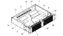
- FIG. 2 is a view of the patch panel of FIG. 1 with the lid removed.
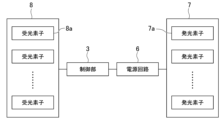
- 1 is a block diagram showing a configuration of a patch panel according to an embodiment of the present invention.
- FIG. 2 is a schematic diagram showing a waveguide according to the present embodiment.
- 5 is a cross-sectional view taken along the line VV in FIG. 4.
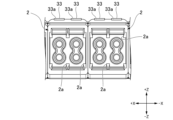
- FIG. 2 is an enlarged view of the periphery of the adapter in FIG. 1 .
- 1 is a perspective view of an optical connector according to an embodiment of the present invention.
- 1 is a cross-sectional view of an optical connector according to an embodiment of the present invention.
- FIG. 11 is an enlarged view of the periphery of an adapter according to a modified example of the embodiment.
- the optical connection system 100 includes a patch panel P and a plurality of optical connectors 10.
- the patch panel P includes a housing 1 and a plurality of adapters 2.
- the housing 1 has a pair of side walls 1a, a cover 1b, a bottom wall 1c, and a rear wall 1d.
- a control unit 3 Inside the housing 1, a control unit 3, a power supply circuit 6, a light source 7, a light receiving unit 8, a waveguide 30, etc. are arranged inside the housing 1, a control unit 3, a power supply circuit 6, a light source 7, a light receiving unit 8, a waveguide 30, etc. are arranged inside the housing 1, a control unit 3, a power supply circuit 6, a light source 7, a light receiving unit 8, a waveguide 30, etc. are arranged inside the housing 1, a control unit 3, a power supply circuit 6, a light source 7, a light receiving unit 8, a waveguide 30, etc. are arranged inside the housing 1, a control unit 3, a power supply circuit 6, a light source 7, a light receiving unit 8,
- An optical connector 10 is connected to the adapter 2. Although omitted in FIG. 2, an optical circuit (e.g., multiple optical fibers) for optically connecting the adapter (first adapter) 2 and the second adapter 4 is provided inside the housing 1.
- the optical connection system 100 is configured to optically connect the optical connector 10 connected to the adapter 2 and the second adapter 4. Such an optical connection system 100 is disposed, for example, in a data center or the like.
- the adapter 2 has a socket 2a (see FIG. 6) into which the optical connector 10 is inserted.
- the front side the side to which the socket 2a faces (-Y side)
- the opposite side (+Y side) is called the back side.
- a direction perpendicular to the front-rear direction Y is called the left-right direction X.
- One side (+X side) in the left-right direction X is called the left side
- the opposite side (-X side) is called the right side.
- a direction perpendicular to both the front-rear direction Y and the left-right direction X is called the up-down direction Z.
- the side where the cover 1b is arranged (+Z side) is called the upper side
- the side where the bottom wall 1c is arranged (-Z side) is called the lower side.
- the up-down direction Z does not have to coincide with the vertical direction.
- the multiple adapters 2 are arranged at the front end of the patch panel P. These adapters 2 are arranged side by side in both the left-right direction X and the up-down direction Z.
- the patch panel P has multiple waveguides 30 corresponding to the number of connectable optical connectors 10. Note that in FIG. 2, only one waveguide 30 is shown, and the remaining waveguides 30 are omitted.
- the waveguide 30 has a first branch 31, a second branch 32, a main waveguide portion 33, and a branch portion 34.
- the first branch 31, the second branch 32, and the main waveguide portion 33 are, for example, optical fibers made of plastic.
- the first branch 31, the second branch 32, and the main waveguide portion 33 may be optical fibers made of glass.
- a part or the whole of the waveguide 30 may be a planar optical waveguide.
- FIG. 3 is a functional block diagram of the patch panel P.
- the control unit 3 is electrically connected to the light receiving unit 8.
- the control unit 3 is also electrically connected to the light source 7 via the power supply circuit 6.
- the patch panel P has wiring for electrically connecting the control unit 3, the power supply circuit 6, the light source 7, the light receiving unit 8, etc.
- the control unit 3 includes hardware such as a CPU (Central Processing Unit) and an ASIC (Application Specific Integrated Circuit).
- the light source 7 includes a plurality of light emitting elements 7a.
- the light receiving unit 8 includes a plurality of light receiving elements 8a.
- the control unit 3 controls the power supply circuit 6 to switch the state of the light-emitting element 7a of the light source 7. For example, the control unit 3 may switch the state of the light-emitting element 7a depending on the light detection results of the multiple light-receiving elements 8a.
- the "state of the light-emitting element 7a" refers to on, off, blinking, color, etc.
- the control unit 3 may also communicate with the outside. The control unit 3 may then switch the state of the light-emitting element 7a based on a command from the outside.
- the "outside" may be, for example, a system that oversees the operation of a data center.
- the light-emitting elements 7a and the sockets 2a correspond one-to-one.
- a bicolor LED is used as the light-emitting element 7a.
- a bicolor LED is a type of LED (Light Emitting Diode) that can emit two different colors.
- the two different colors are referred to as the "first display color” and the "second display color", respectively.
- the patch panel P is configured to display a first display color or a second display color on each light-emitting unit 33a (described later) according to the connection status of the optical connector 10 to each socket 2a. For example, when the optical connector 10 is not connected to any socket 2a, the light-emitting unit 33a corresponding to that socket 2a displays the first display color. Alternatively, when the optical connector 10 is connected to the socket 2a, the light-emitting unit 33a corresponding to that socket 2a displays the second display color. For example, the first display color is red, and the second display color is green.
- the combination of the first and second display colors can be changed. Yellow, blue, white, etc. may be used.
- the state of the corresponding socket 2a may be displayed by changing the lighting state of the light-emitting element 7a. Lighting states include, for example, continuous lighting, blinking (repeated lighting and turning off), etc.
- the light-emitting element 7a may be an LED other than a two-color LED, or may not be an LED.
- the light source 7 may have multiple light-emitting elements 7a of different types (colors). Then, multiple light-emitting elements 7a of different types (colors) may emit light into one waveguide 30. In this case, the waveguide 30 may have multiple first branch paths 31, which will be described later.
- the multiple light receiving elements 8a and the multiple sockets 2a are in one-to-one correspondence.
- the light receiving elements 8a can detect light. More specifically, the light receiving elements 8a generate an electrical signal by receiving light. The electrical signal generated by the light receiving elements 8a is input to the control unit 3.
- a photodiode can be used as the light receiving elements 8a. The function of the light receiving elements 8a in the patch panel P will be described later.
- FIG 4 is a schematic diagram showing the connection relationship between the waveguide 30, the light-emitting element 7a, the light-receiving element 8a, and the optical connector 10.
- the first branch 31, the second branch 32, and the main waveguide portion 33 are depicted in a simplified linear form.
- each portion of the waveguide 30 is curved and arranged inside the housing 1.
- a large number of waveguides 30 are arranged inside the housing 1. Therefore, in order to make effective use of the space, each portion of the waveguide 30 (the first branch 31, the second branch 32, and the main waveguide portion 33) is curved and arranged.
- the length of each portion of the waveguide 30 can be changed as appropriate.
- FIG. 5 is a cross-sectional view taken along the line V-V in FIG. 4.
- the branch section 34 has a sheath 34a.
- the sheath 34a houses the respective ends of the first branch path 31, the second branch path 32, and the main wave section 33.
- the sheath 34a maintains the first branch path 31 and the second branch path 32 in a state where they are optically connected to the main wave section 33.
- the sheath 34a is a rectangular tube.
- the shape of the sheath 34a may be changed.
- the sheath 34a may be cylindrical.
- the outer diameter of the main wave section 33 is larger than the outer diameter of the first branch path 31 and the outer diameter of the second branch path 32.
- the main wave section 33 is an optical fiber with an outer diameter of 0.75 mm
- the first branch path 31 and the second branch path 32 are optical fibers with an outer diameter of 0.5 mm.
- the main waveguide section 33, the first branch path 31 and the second branch path 32 are realized by, for example, plastic fibers, which allows them to be constructed at a lower cost than when glass fibers are used.
- the branching section 34 In the branching section 34, the end face of the first branching path 31 is abutted against the end face of the main wave section 33. Therefore, the light emitted by the light-emitting element 7a propagates through the first branching path 31 toward the branching section 34 and enters the main wave section 33. Similarly, the end face of the second branching path 32 is abutted against the end face of the main wave section 33. Therefore, the return light (described later) that propagates through the main wave section 33 toward the branching section 34 enters the second branching path 32.
- the structure of the branching section 34 can be changed.
- the first branching path 31 and the second branching path 32 may be fusion-spliced to the main wave section 33.
- FIG. 6 is an enlarged view of the adapter 2 seen from the front side.
- the adapter 2 has a socket 2a for inserting the optical connector 10.
- one adapter 2 has two sockets 2a for a duplex type connector as an example.
- two optical connectors 10 can be connected to one adapter 2.
- the light-emitting portion 33a of the main wave portion 33 is disposed above each socket 2a of the adapter 2.
- the socket 2a and the light-emitting portion 33a correspond one-to-one.
- the light-emitting portion 33a is an end face of the main wave portion 33.
- the light emitted by the light-emitting element 7a propagates through the main wave portion 33 and is radiated from the light-emitting portion 33a.
- the number of sockets 2a that the adapter 2 has may be one. In this case, the adapter 2 and the light-emitting portion 33a correspond one-to-one.
- the optical connector 10 has two ferrules 11, two optical fibers 12, a housing 13, a locking projection 14, a boot 15, and a waveguide member 20.
- the number of ferrules 11 and optical fibers 12 in the optical connector 10 may be one or three or more.
- the ferrule 11 has a connection end face 11a facing the rear side (+Y side).
- the ferrule 11 has an insertion hole for inserting the optical fiber 12. This insertion hole opens in the connection end face 11a of the ferrule 11.
- the optical fiber 12 is exposed at the connection end face 11a.
- the optical connector 10 has a biasing member for biasing the ferrule 11 toward the connection end face 11a.
- the housing 13 houses the biasing member, the ferrule 11, etc. inside.
- the locking projection 14 protrudes upward from the housing 13.
- the locking projection 14 fits into a locking hole in the adapter 2. This determines the position of the optical connector 10 relative to the adapter 2.
- the boot 15 is located closer to the front (-Y side) than the housing 13.
- the boot 15 is made of an elastic material.
- a cable portion extends from the boot 15 toward the front.
- the cable portion has an outer sheath that houses the optical fiber 12.
- the waveguide 20 is located above the housing 13 and the boot 15. As shown in Figs. 7 and 8, the waveguide 20 has a first waveguide 21 and a second waveguide 22.
- the first waveguide 21 extends linearly in the front-rear direction Y.
- the waveguide 21 has an incident surface 21a.
- the incident surface 21a is an end surface of the first waveguide 21 facing the rear side (+Y side).
- a reflector 24 is provided on a part of the incident surface 21a.
- a mirror is used as the reflector 24.
- the mirror as the reflector 24 is attached to the incident surface 21a.
- the reflector 24 may be formed by plating a part of the incident surface 21a, for example.
- the second waveguide 22 is inclined downward as it approaches the front side.
- the second waveguide 22 is connected to the front end of the first waveguide 21.
- the first waveguide 21 and the second waveguide 22 guide light inside.
- the first waveguide 21 and the second waveguide 22 can be made of a material such as a transparent resin.
- the bottom surface of the second waveguide 22 is used as a scattering section 23 that scatters light.
- the incident surface 21a and the reflecting section 24 face the light emitting section 33a of the main waveguide section 33 (see Figures 4 and 6).
- the scattering section 23 faces the boot 15.
- the optical connection system 100 has a function of displaying the connection status of the optical connector 10 to the socket 2a using the light-emitting unit 33a. This function is called the housing-side display function.
- the optical connection system 100 also has a function of displaying the connection status using the scattering unit 23. This function is called the connector-side display function.
- the "connection status" can include, for example, a "non-connection state,” a "connection state,” an "alert state,” and the like.
- the “non-connection state” is a state in which the optical connector 10 is not connected to any socket 2a.
- the “connection state” is a state in which the optical connector 10 is normally connected to any socket 2a.
- the “alert state” is a state in which the optical connector 10 is connected to any socket 2a, but a network malfunction has occurred, for example, and maintenance is recommended. A more detailed description will be given below.
- the control unit 3 causes the multiple light-emitting elements 7a of the light source 7 to emit light in the first display color via the power supply circuit 6. At this time, all the light-emitting elements 7a may be caused to emit light. Alternatively, only the light-emitting elements 7a corresponding to the sockets 2a that may be used may be caused to emit light.
- the light of the first display color emitted by the light-emitting elements 7a passes through the first branch path 31 of the corresponding waveguide 30 and enters the main waveguide portion 33. The light of the first display color also reaches the light-emitting portion 33a (the end surface of the main waveguide portion 33).
- the reflecting portion 24 and the light emitting portion 33a of the optical connector 10 face each other. Therefore, a part of the light emitted from the light emitting portion 33a is reflected by the reflecting portion 24 and enters the main wave portion 33 again.
- the light reflected by the reflecting portion 24 is called "return light.”
- the return light travels through the main wave portion 33 toward the branching portion 34, and enters the second branching path 32 at the branching portion 34.
- the return light further travels through the second branching path 32 and enters the light receiving element 8a.
- the light receiving element 8a generates an electrical signal by receiving the return light, and inputs it to the control unit 3. This allows the control unit 3 to determine that the optical connector 10 has been inserted into the receptacle 2a corresponding to the light receiving element 8a.
- the control unit 3 causes the light-emitting element 7a corresponding to the socket 2a into which the optical connector 10 is inserted to emit light in the second display color.
- the light of the target light-emitting element 7a is switched from the first display color to the second display color.
- This causes the light-emitting unit 33a to emit light of the second display color.
- the light-emitting unit 33a corresponding to the socket 2a into which the optical connector 10 is not inserted continues to emit light of the first display color.
- the optical connection system 100 can cause the multiple light-emitting units 33a of the patch panel P to emit light in the first display color and the second display color depending on the connected state and the non-connected state.
- the control unit 3 may also cause the light emitting unit 33a of the socket 2a that is the target of maintenance to flash in the first display color or the second display color. This allows the user to grasp the connection status of multiple sockets 2a as follows: 1st display color (continuously lit): connected state 2nd display color (continuously lit): not connected state 1st display color or 2nd display color (blinking): alert state
- connection status of multiple sockets 2a In data centers and the like, the user can easily grasp the connection status of multiple sockets 2a, thereby improving work efficiency.
- the above-mentioned method of displaying the connection status is one example and can be modified as appropriate.
- a method of alternately lighting the first display color and the second display color may also be added, thereby displaying four or more types of status.
- the blinking pattern (time interval, etc.) of the first display color or the second display color may also be changed.
- the light emitted from the light-emitting unit 33a corresponds to the connection status. Therefore, the user can grasp the connection status by visually checking the light scattered in the scattering unit 23.
- the visibility of the light can be increased by scattering the light with the scattering unit 23 provided on the optical connector 10.
- the boot 15 located at the front end of the optical connector 10 appears to be emitting light, thereby further increasing visibility.
- the patch panel P includes an adapter 2 having a socket 2a into which an optical connector 10 is inserted, a light emitting unit 33a arranged adjacent to the socket 2a, a light source 7 that emits light, a light receiving element 8a that detects the light, and a waveguide 30.
- the waveguide 30 has a branching unit 34, a first branching path 31 that guides the light emitted by the light source 7 to the branching unit 34, a main waveguide unit 33 that guides the light guided by the first branching path 31 to the light emitting unit 33a, and a second branching path 32 that guides the light guided by the main waveguide unit 33 toward the branching unit 34 to the light receiving element 8a.
- connection status of the socket 2a can be recognized by the user by illuminating the light emitting unit 33a arranged adjacent to the socket 2a.
- the return light reflected by the optical connector 10 can be guided to the light receiving element 8a using the waveguide 30. Therefore, the light receiving element 8a can be used to detect whether the optical connector 10 is connected or not.
- the patch panel P also includes a control unit 3 that controls the light source 7 based on the light detection results from the light receiving element 8a.
- a control unit 3 controls the light source 7 based on the light detection results from the light receiving element 8a.
- the light source 7 can also emit two different colors. Specifically, the light source 7 can have a light-emitting element 7a that is a two-color LED. Alternatively, the light source 7 can have multiple types of light-emitting elements 7a that emit different colors. In these cases, the color of the light in the light-emitting section 33a can be switched depending on the connection status of the optical connector 10 to the socket 2a. In other words, the connection status can be indicated to the user using different colors.
- the control unit 3 also switches the color of light emitted by the light source 7 based on the light detection results from the light receiving element 8a. With this configuration, the color of light from the light emitting unit 33a can be automatically switched.
- the main wave portion 33 is an optical fiber
- the light emitting portion 33a is an end face of the optical fiber (main wave portion 33).
- the light emitting portion 33a can be arranged in a small space around the adapter 2. Therefore, the size of the patch panel P can be reduced.
- the light emitting portion 33a can be provided without arranging a board or the like around the adapter 2. This makes it possible to increase the density of the adapters 2 in the patch panel P, and the optical connectors 10 can be connected at high density.
- the light emitting portion 33a may have a flat shape when viewed from the front-rear direction Y. More specifically, the light emitting portion 33a of this modified example has a smaller dimension in the up-down direction Z than in the left-right direction X.
- Such a light emitting portion 33a can be formed, for example, by the following methods. As a first method, the end portion on the front side (-Y side) of the member (e.g., a plastic optical fiber) that becomes the main wave portion 33 may be deformed. When deforming, the member that becomes the main wave portion 33 may be heated and softened, and pressure may be applied in the up-down direction Z.
- the member e.g., a plastic optical fiber
- the front end of the material that will become the main wave portion 33 may be machined.
- a flat material may be used as the main wave portion 33.
- the main wave portion 33 has a flat shape in the vicinity of the light emitting portion 33a, and the other portion has a cylindrical shape.
- the entire main wave portion 33 has a flat shape.
- the light-emitting portion 33a flat, it is possible to arrange multiple adapters 2 at small intervals in the vertical direction Z. In other words, it is possible to arrange more adapters 2 closer together in the vertical direction Z. This makes it possible to increase the number of optical connectors 10 that can be connected to the patch panel P.
- the waveguide member 20 may be integrated with the boot 15 located in front of the housing 13.
- the boot 15 itself may be formed from a material capable of guiding light (e.g., transparent resin).
- the boot 15 may have an incident surface, a waveguide section that guides the light incident from the incident surface toward the side opposite the connection end surface, and a scattering section that scatters the light guided by the waveguide section. In this case as well, the same effect as in the above embodiment can be obtained.
- the control unit 3 described above has a computer system inside.
- a program for implementing the functions of the control unit 3 may be recorded on a computer-readable recording medium, and the program may be read into the computer system and executed to perform processing in the control unit 3.
Landscapes
- Physics & Mathematics (AREA)
- General Physics & Mathematics (AREA)
- Optics & Photonics (AREA)
- Mechanical Coupling Of Light Guides (AREA)
- Optical Couplings Of Light Guides (AREA)
Priority Applications (2)
| Application Number | Priority Date | Filing Date | Title |
|---|---|---|---|
| US19/151,019 US20260227590A1 (en) | 2023-01-27 | 2023-11-08 | Patch panel |
| JP2024572848A JP7879283B2 (ja) | 2023-01-27 | 2023-11-08 | パッチパネル |
Applications Claiming Priority (2)
| Application Number | Priority Date | Filing Date | Title |
|---|---|---|---|
| JP2023011164 | 2023-01-27 | ||
| JP2023-011164 | 2023-01-27 |
Publications (1)
| Publication Number | Publication Date |
|---|---|
| WO2024157569A1 true WO2024157569A1 (ja) | 2024-08-02 |
Family
ID=91970210
Family Applications (1)
| Application Number | Title | Priority Date | Filing Date |
|---|---|---|---|
| PCT/JP2023/040191 Ceased WO2024157569A1 (ja) | 2023-01-27 | 2023-11-08 | パッチパネル |
Country Status (3)
| Country | Link |
|---|---|
| US (1) | US20260227590A1 (cg-RX-API-DMAC7.html) |
| JP (1) | JP7879283B2 (cg-RX-API-DMAC7.html) |
| WO (1) | WO2024157569A1 (cg-RX-API-DMAC7.html) |
Citations (6)
| Publication number | Priority date | Publication date | Assignee | Title |
|---|---|---|---|---|
| JPH09508980A (ja) * | 1994-02-15 | 1997-09-09 | データ スウイツチ コーポレーシヨン | 光ファイバー接続モニター装置、パッチパネル制御システムならびにその使用法 |
| JP2005109598A (ja) * | 2003-09-29 | 2005-04-21 | Shoden Corp | 光通信機器用モニタ装置 |
| JP2007057642A (ja) * | 2005-08-23 | 2007-03-08 | Hitachi Metals Ltd | 光パッチパネル |
| US20170139165A1 (en) * | 2015-11-12 | 2017-05-18 | Facebook, Inc. | Modular monitored patch panel system |
| JP2018205664A (ja) * | 2017-06-09 | 2018-12-27 | 岡野電線株式会社 | 光ファイバケーブル |
| US20200166718A1 (en) * | 2018-11-28 | 2020-05-28 | Go!Foton Holdings, Inc. | Intelligent patch panel |
-
2023
- 2023-11-08 WO PCT/JP2023/040191 patent/WO2024157569A1/ja not_active Ceased
- 2023-11-08 US US19/151,019 patent/US20260227590A1/en active Pending
- 2023-11-08 JP JP2024572848A patent/JP7879283B2/ja active Active
Patent Citations (6)
| Publication number | Priority date | Publication date | Assignee | Title |
|---|---|---|---|---|
| JPH09508980A (ja) * | 1994-02-15 | 1997-09-09 | データ スウイツチ コーポレーシヨン | 光ファイバー接続モニター装置、パッチパネル制御システムならびにその使用法 |
| JP2005109598A (ja) * | 2003-09-29 | 2005-04-21 | Shoden Corp | 光通信機器用モニタ装置 |
| JP2007057642A (ja) * | 2005-08-23 | 2007-03-08 | Hitachi Metals Ltd | 光パッチパネル |
| US20170139165A1 (en) * | 2015-11-12 | 2017-05-18 | Facebook, Inc. | Modular monitored patch panel system |
| JP2018205664A (ja) * | 2017-06-09 | 2018-12-27 | 岡野電線株式会社 | 光ファイバケーブル |
| US20200166718A1 (en) * | 2018-11-28 | 2020-05-28 | Go!Foton Holdings, Inc. | Intelligent patch panel |
Also Published As
| Publication number | Publication date |
|---|---|
| JPWO2024157569A1 (cg-RX-API-DMAC7.html) | 2024-08-02 |
| US20260227590A1 (en) | 2026-08-06 |
| JP7879283B2 (ja) | 2026-06-23 |
Similar Documents
| Publication | Publication Date | Title |
|---|---|---|
| US7194183B2 (en) | Modular receptacle assembly and interface with integral optical indication | |
| US6352446B2 (en) | Modular jack assembly having light transmission means with a light indicator | |
| US10222561B2 (en) | Light launch device for transmitting light into a traceable fiber optic cable assembly with tracing optical fibers | |
| US6334012B1 (en) | Optical connector module | |
| US8638233B2 (en) | Cable connection component configured to provide visible indications | |
| US10101545B2 (en) | Traceable cable assembly and connector | |
| TWM463356U (zh) | 可追踪型線纜裝置 | |
| US20170207585A1 (en) | Traceable cable system, traceable cable assembly and connector | |
| US7447440B2 (en) | Multiple channel optical transceiver modules | |
| US10234614B2 (en) | Light source assemblies and systems and methods with mode homogenization | |
| EP0945933B1 (en) | Modular jack assembly with indicator | |
| JP4872941B2 (ja) | 光通信モジュール及びその使用方法 | |
| CN104968530B (zh) | 具有光显示的连接模块 | |
| JP7084263B2 (ja) | 光コネクタプラグの接続検知機構 | |
| WO2024157568A1 (ja) | 光コネクタ | |
| US5812730A (en) | Light dissipating spring interconnection between lightguides | |
| US8287302B2 (en) | Cable end connectors | |
| CN100403083C (zh) | 用于光背板的模块系统 | |
| KR102159330B1 (ko) | 엘이디 어댑터가 구비된 패치 코드 | |
| KR102802207B1 (ko) | 광전 센서 | |
| JP4587653B2 (ja) | 光通信機器用モニタ装置 | |
| US20250202585A1 (en) | Connectivity indicators in communication systems | |
| JP2001013376A (ja) | 光コネクタ及び光伝送モジュール | |
| WO2025178178A1 (ko) | 전자 제품용 컨트롤 패널 | |
| JP2002243989A (ja) | 光半導体モジュール |
Legal Events
| Date | Code | Title | Description |
|---|---|---|---|
| 121 | Ep: the epo has been informed by wipo that ep was designated in this application |
Ref document number: 23918524 Country of ref document: EP Kind code of ref document: A1 |
|
| ENP | Entry into the national phase |
Ref document number: 2024572848 Country of ref document: JP Kind code of ref document: A |
|
| WWE | Wipo information: entry into national phase |
Ref document number: 2024572848 Country of ref document: JP |
|
| NENP | Non-entry into the national phase |
Ref country code: DE |
|
| 122 | Ep: pct application non-entry in european phase |
Ref document number: 23918524 Country of ref document: EP Kind code of ref document: A1 |