WO2024157505A1 - 電子部品及び電子部品の製造方法 - Google Patents
電子部品及び電子部品の製造方法 Download PDFInfo
- Publication number
- WO2024157505A1 WO2024157505A1 PCT/JP2023/030254 JP2023030254W WO2024157505A1 WO 2024157505 A1 WO2024157505 A1 WO 2024157505A1 JP 2023030254 W JP2023030254 W JP 2023030254W WO 2024157505 A1 WO2024157505 A1 WO 2024157505A1
- Authority
- WO
- WIPO (PCT)
- Prior art keywords
- element body
- protective material
- electronic component
- metal alkoxide
- voids
- Prior art date
- Legal status (The legal status is an assumption and is not a legal conclusion. Google has not performed a legal analysis and makes no representation as to the accuracy of the status listed.)
- Ceased
Links
Images





Classifications
-
- H—ELECTRICITY
- H01—ELECTRIC ELEMENTS
- H01C—RESISTORS
- H01C1/00—Details
- H01C1/02—Housing; Enclosing; Embedding; Filling the housing or enclosure
- H01C1/034—Housing; Enclosing; Embedding; Filling the housing or enclosure the housing or enclosure being formed as coating or mould without outer sheath
-
- C—CHEMISTRY; METALLURGY
- C03—GLASS; MINERAL OR SLAG WOOL
- C03C—CHEMICAL COMPOSITION OF GLASSES, GLAZES OR VITREOUS ENAMELS; SURFACE TREATMENT OF GLASS; SURFACE TREATMENT OF FIBRES OR FILAMENTS MADE FROM GLASS, MINERALS OR SLAGS; JOINING GLASS TO GLASS OR OTHER MATERIALS
- C03C1/00—Ingredients generally applicable to manufacture of glasses, glazes, or vitreous enamels
- C03C1/006—Ingredients generally applicable to manufacture of glasses, glazes, or vitreous enamels to produce glass through wet route
-
- H—ELECTRICITY
- H01—ELECTRIC ELEMENTS
- H01C—RESISTORS
- H01C1/00—Details
- H01C1/02—Housing; Enclosing; Embedding; Filling the housing or enclosure
- H01C1/028—Housing; Enclosing; Embedding; Filling the housing or enclosure the resistive element being embedded in insulation with outer enclosing sheath
-
- H—ELECTRICITY
- H01—ELECTRIC ELEMENTS
- H01C—RESISTORS
- H01C1/00—Details
- H01C1/14—Terminals or tapping points specially adapted for resistors; Arrangements of terminals or tapping points on resistors
- H01C1/142—Terminals or tapping points specially adapted for resistors; Arrangements of terminals or tapping points on resistors the terminals or tapping points being coated on the resistive element
-
- H—ELECTRICITY
- H01—ELECTRIC ELEMENTS
- H01C—RESISTORS
- H01C17/00—Apparatus or processes specially adapted for manufacturing resistors
- H01C17/02—Apparatus or processes specially adapted for manufacturing resistors adapted for manufacturing resistors with envelope or housing
-
- H—ELECTRICITY
- H01—ELECTRIC ELEMENTS
- H01C—RESISTORS
- H01C17/00—Apparatus or processes specially adapted for manufacturing resistors
- H01C17/28—Apparatus or processes specially adapted for manufacturing resistors adapted for applying terminals
- H01C17/281—Apparatus or processes specially adapted for manufacturing resistors adapted for applying terminals by thick film techniques
-
- H—ELECTRICITY
- H01—ELECTRIC ELEMENTS
- H01C—RESISTORS
- H01C7/00—Non-adjustable resistors formed as one or more layers or coatings; Non-adjustable resistors made from powdered conducting material or powdered semi-conducting material with or without insulating material
- H01C7/04—Non-adjustable resistors formed as one or more layers or coatings; Non-adjustable resistors made from powdered conducting material or powdered semi-conducting material with or without insulating material having negative temperature coefficient
-
- H—ELECTRICITY
- H01—ELECTRIC ELEMENTS
- H01C—RESISTORS
- H01C7/00—Non-adjustable resistors formed as one or more layers or coatings; Non-adjustable resistors made from powdered conducting material or powdered semi-conducting material with or without insulating material
- H01C7/04—Non-adjustable resistors formed as one or more layers or coatings; Non-adjustable resistors made from powdered conducting material or powdered semi-conducting material with or without insulating material having negative temperature coefficient
- H01C7/041—Non-adjustable resistors formed as one or more layers or coatings; Non-adjustable resistors made from powdered conducting material or powdered semi-conducting material with or without insulating material having negative temperature coefficient formed with two or more layers
-
- H—ELECTRICITY
- H01—ELECTRIC ELEMENTS
- H01F—MAGNETS; INDUCTANCES; TRANSFORMERS; SELECTION OF MATERIALS FOR THEIR MAGNETIC PROPERTIES
- H01F27/00—Details of transformers or inductances, in general
- H01F27/02—Casings
-
- H—ELECTRICITY
- H01—ELECTRIC ELEMENTS
- H01G—CAPACITORS; CAPACITORS, RECTIFIERS, DETECTORS, SWITCHING DEVICES, LIGHT-SENSITIVE OR TEMPERATURE-SENSITIVE DEVICES OF THE ELECTROLYTIC TYPE
- H01G4/00—Fixed capacitors; Processes of their manufacture
- H01G4/002—Details
- H01G4/224—Housing; Encapsulation
-
- H—ELECTRICITY
- H01—ELECTRIC ELEMENTS
- H01G—CAPACITORS; CAPACITORS, RECTIFIERS, DETECTORS, SWITCHING DEVICES, LIGHT-SENSITIVE OR TEMPERATURE-SENSITIVE DEVICES OF THE ELECTROLYTIC TYPE
- H01G4/00—Fixed capacitors; Processes of their manufacture
- H01G4/002—Details
- H01G4/228—Terminals
- H01G4/232—Terminals electrically connecting two or more layers of a stacked or rolled capacitor
-
- H—ELECTRICITY
- H01—ELECTRIC ELEMENTS
- H01G—CAPACITORS; CAPACITORS, RECTIFIERS, DETECTORS, SWITCHING DEVICES, LIGHT-SENSITIVE OR TEMPERATURE-SENSITIVE DEVICES OF THE ELECTROLYTIC TYPE
- H01G4/00—Fixed capacitors; Processes of their manufacture
- H01G4/002—Details
- H01G4/228—Terminals
- H01G4/232—Terminals electrically connecting two or more layers of a stacked or rolled capacitor
- H01G4/2325—Terminals electrically connecting two or more layers of a stacked or rolled capacitor characterised by the material of the terminals
-
- H—ELECTRICITY
- H01—ELECTRIC ELEMENTS
- H01G—CAPACITORS; CAPACITORS, RECTIFIERS, DETECTORS, SWITCHING DEVICES, LIGHT-SENSITIVE OR TEMPERATURE-SENSITIVE DEVICES OF THE ELECTROLYTIC TYPE
- H01G4/00—Fixed capacitors; Processes of their manufacture
- H01G4/30—Stacked capacitors
-
- C—CHEMISTRY; METALLURGY
- C03—GLASS; MINERAL OR SLAG WOOL
- C03C—CHEMICAL COMPOSITION OF GLASSES, GLAZES OR VITREOUS ENAMELS; SURFACE TREATMENT OF GLASS; SURFACE TREATMENT OF FIBRES OR FILAMENTS MADE FROM GLASS, MINERALS OR SLAGS; JOINING GLASS TO GLASS OR OTHER MATERIALS
- C03C2201/00—Glass compositions
- C03C2201/60—Glass compositions containing organic material
-
- C—CHEMISTRY; METALLURGY
- C03—GLASS; MINERAL OR SLAG WOOL
- C03C—CHEMICAL COMPOSITION OF GLASSES, GLAZES OR VITREOUS ENAMELS; SURFACE TREATMENT OF GLASS; SURFACE TREATMENT OF FIBRES OR FILAMENTS MADE FROM GLASS, MINERALS OR SLAGS; JOINING GLASS TO GLASS OR OTHER MATERIALS
- C03C2203/00—Production processes
- C03C2203/20—Wet processes, e.g. sol-gel process
- C03C2203/26—Wet processes, e.g. sol-gel process using alkoxides
Definitions
- This disclosure relates to electronic components and methods for manufacturing electronic components.
- Patent Document 1 The electronic component described in Patent Document 1 comprises an element body, a protective material that covers the outer surface of the element body, and an external electrode that covers part of the outer surface of the protective material.
- the element body is porous and has voids inside.
- Patent Document 1 also discloses a glass film as an example of the protective material.
- the glass film disclosed in Patent Document 1 as a protective material tends to remain on the outer surface of the element during the manufacturing process of the glass film. This makes it difficult to fill voids inside the element with glass. As a result, voids tend to remain inside the element, and cracks and the like are likely to occur in the element starting from the voids.
- one aspect of the present disclosure is an electronic component having an element body, a protective material covering all or part of the outer surface of the element body, and an external electrode covering part of the outer surface of the protective material, the element body having a plurality of voids therein, the protective material being glass containing a silane compound having a carbon chain with three or more carbon atoms, a filling portion filling at least some of the voids, and a film portion covering the outer surface of the element body.
- An aspect of the present disclosure is a method for manufacturing an electronic component, comprising: an element preparation step of preparing an element having a plurality of voids therein; an element introduction step of introducing the element into a reaction vessel; a solution introduction step of introducing a solution containing a metal alkoxide or a metal alkoxide precursor and a silane compound having a carbon chain with three or more carbon atoms into the reaction vessel; and a protective material formation step of hydrolyzing and dehydrating and condensing the metal alkoxide on the outer surface of the element, and forming a protective material consisting of a filling portion that fills the plurality of voids and a film portion that covers the outer surface of the element.
- the protective material is glass containing a silane compound. And because this silane compound has a carbon chain with three or more carbon atoms, the glass easily penetrates into the voids inside the element during the manufacturing process of the protective material. As a result, the protective material has not only a film portion that covers the outer surface of the element, but also a filling portion that fills the voids. In this way, if the filling portion, which is part of the protective material, fills the voids in the element, it is possible to prevent cracks and the like from occurring in the element starting from the voids in the element.
- the strength of the element can be improved.
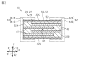
- FIG. FIG. 3 is a cross-sectional view taken along line 3-3 in FIG. 2.
- FIG. 2 is an enlarged cross-sectional view of the vicinity of a film portion of the electronic component.
- 1A to 1C are explanatory diagrams illustrating a manufacturing method of an electronic component.
- 1A to 1C are explanatory diagrams illustrating a manufacturing method of an electronic component.
- 1A to 1C are explanatory diagrams illustrating a manufacturing method of an electronic component.
- 1A to 1C are explanatory diagrams illustrating a manufacturing method of an electronic component.
- 1A to 1C are explanatory diagrams illustrating a manufacturing method of an electronic component.
- the electronic component 10 is, for example, a surface-mount type negative temperature coefficient thermistor component that is mounted on a circuit board, etc. Note that a negative temperature coefficient thermistor component has a characteristic that its resistance value decreases as the temperature increases.
- the electronic component 10 includes an element body 20.
- the element body 20 is generally rectangular prism-shaped and has a central axis CA.
- an axis extending along the central axis CA is defined as a first axis X.
- One of the axes perpendicular to the first axis X is defined as a second axis Y.
- An axis perpendicular to the first axis X and the second axis Y is defined as a third axis Z.
- One of the directions along the first axis X is defined as a first positive direction X1
- the direction along the first axis X opposite to the first positive direction X1 is defined as a first negative direction X2.
- One of the directions along the second axis Y is defined as a second positive direction Y1, and the direction along the second axis Y opposite to the second positive direction Y1 is defined as a second negative direction Y2.
- One of the directions along the third axis Z is defined as a third positive direction Z1, and the direction along the third axis Z opposite to the third positive direction Z1 is defined as a third negative direction Z2.
- the outer surface 21 of the element body 20 has six flat surfaces 22.
- the "surface” of the element body 20 here refers to a surface that can be observed when the entire element body 20 is observed. In other words, even if there are minute irregularities or steps that can only be seen by magnifying and observing a part of the element body 20 with a microscope, the surface is expressed as a flat surface or a curved surface.
- the six flat surfaces 22 face in different directions.
- the six flat surfaces 22 are broadly divided into a first end surface 22A facing the first positive direction X1, a second end surface 22B facing the first negative direction X2, and four side surfaces 22C.
- the four side surfaces 22C are a surface facing the third positive direction Z1, a surface facing the third negative direction Z2, a surface facing the second positive direction Y1, and a surface facing the second negative direction Y2, respectively.
- the boundary portions between two adjacent flat surfaces 22 and the boundary portions between three adjacent surfaces are curved.
- the corners of the element body 20 are rounded and chamfered.
- the outer surface 53 of the film portion 51 in the protective material 50 which will be described later, is identified with the outer surface 21 of the element body 20 and is given a reference number.
- the element body 20 has a larger dimension along the first axis X than along the third axis Z. Also, as shown in FIG. 3, the element body 20 has a larger dimension along the first axis X than along the second axis Y.
- the material of the element body 20 is a ceramic obtained by sintering a metal oxide containing one or more elements selected from Mn, Fe, Ni, Co, Ti, Ba, Al, and Zn. Therefore, as shown in FIG. 4, the element body 20 has a plurality of voids 23 inside. These voids 23 exist mainly at the boundaries of the grains that make up the element body 20, which is a sintered body. Note that the voids 23 are not shown in FIG. 3.
- the ratio of the total volume of the voids 23 to the volume of the element body 20 is defined as the porosity.
- the volume of the element body 20 includes the volume of the voids 23 in addition to the volume of the ceramic portion.
- the porosity is 0.5% to 2.5%.
- the porosity is calculated as follows. First, an electron microscope is used to image a 10 ⁇ m square area in any cross section of the element body 20. Similar areas are then imaged in multiple cross sections, and the integrated value of the area of the voids 23 and the integrated value of the area of the 10 ⁇ m square imaged area in the multiple images are calculated. The porosity is then calculated by multiplying the "integrated value of the area of the voids 23/integrated value of the area of the imaged area" by 100. Therefore, in this embodiment, the porosity is expressed as a percentage.
- the electronic component 10 has two first internal electrodes 41 and two second internal electrodes 42.
- the first internal electrodes 41 and the second internal electrodes 42 are both embedded inside the element body 20.
- the material of the first internal electrode 41 is a conductive material.
- the material of the first internal electrode 41 is palladium.
- the material of the second internal electrode 42 is the same as the material of the first internal electrode 41.
- the first internal electrode 41 has a rectangular plate shape.
- the main surface of the first internal electrode 41 is perpendicular to the second axis Y.
- the second internal electrode 42 has the same rectangular plate shape as the first internal electrode 41.
- the main surface of the second internal electrode 42 is perpendicular to the second axis Y, similar to the first internal electrode 41.
- the dimension of the first internal electrode 41 in the direction along the first axis X is smaller than the dimension of the element body 20 in the direction along the first axis X. Also, as shown in FIG. 1, the dimension of the first internal electrode 41 in the direction along the third axis Z is approximately two-thirds of the dimension of the element body 20 in the direction along the third axis Z. The dimensions of the second internal electrode 42 in each direction are the same as those of the first internal electrode 41.
- the first internal electrode 41 and the second internal electrode 42 are positioned alternately in the direction along the second axis Y. That is, from the side surface 22C facing the second positive direction Y1 toward the second negative direction Y2, the first internal electrode 41, the second internal electrode 42, the first internal electrode 41, the second internal electrode 42 are arranged in this order. In this embodiment, the distance between each internal electrode in the direction along the second axis Y is equal.
- the two first internal electrodes 41 and the two second internal electrodes 42 are both located at the center of the element body 20 in the direction along the third axis Z.
- the first internal electrode 41 is located closer to the first positive direction X1.
- the second internal electrode 42 is located closer to the first negative direction X2.
- the end of the first internal electrode 41 on the first positive direction X1 side coincides with the end of the element body 20 on the first positive direction X1 side.
- the end of the first internal electrode 41 on the first positive direction X1 side is exposed at the first end surface 22A of the element body 20.
- the end of the first internal electrode 41 on the first negative direction X2 side is located inside the element body 20 and does not reach the end of the element body 20 on the first negative direction X2 side.
- the end of the second internal electrode 42 on the first negative direction X2 side coincides with the end of the element body 20 on the first negative direction X2 side.
- the end of the first internal electrode 41 on the first negative direction X2 side is exposed at the second end surface 22B of the element body 20.
- the end of the second internal electrode 42 on the first positive direction X1 side is located inside the element body 20 and does not reach the end of the element body 20 on the first positive direction X1 side.
- the electronic component 10 includes a protective material 50.
- the protective material 50 is insulating glass.
- the glass contained in the protective material 50 contains silicon dioxide and a silane compound having a carbon chain with three or more carbon atoms.
- the silane compound that is the material of the protective material 50 has one or more functional groups selected from an epoxy group, a mercapto group, an amino group, a vinyl group, and a methacryl group.
- the silane compound is 3-glycidoxypropyltrimethoxysilane (hereinafter referred to as "GPTMS").
- GPTMS has an epoxy group as a functional group.
- the electronic component 10 has a first external electrode 61 and a second external electrode 62. Note that in FIGS. 1 to 3, the first external electrode 61 and the second external electrode 62 are illustrated by two-dot chain lines.
- the first external electrode 61 has a first base electrode 61A and a first metal layer 61B.
- the first base electrode 61A is laminated on a portion of the outer surface 21 of the element body 20, including the first end face 22A.
- the first base electrode 61A covers the first end face 22A of the element body 20, and also covers a portion of the four side faces 22C in the first positive direction X1 from above the protective material 50.
- the first base electrode 61A is a five-sided electrode.
- the material of the first base electrode 61A is a resin electrode. More specifically, it is a mixture of organic resin and silver particles.
- the first metal layer 61B covers the first base electrode 61A from the outside. Therefore, the first metal layer 61B is laminated on the first base electrode 61A. Although not shown in the figure, the first metal layer 61B has a two-layer structure consisting of a nickel layer and a tin layer, in that order from the first base electrode 61A side.
- the first external electrode 61 is connected to the end of the first internal electrode 41 on the first positive direction X1 side.
- the second external electrode 62 has a second base electrode 62A and a second metal layer 62B.
- the second base electrode 62A is laminated on a portion of the outer surface 21 of the element body 20, including the second end face 22B.
- the second base electrode 62A covers the second end face 22B of the element body 20, and also covers a portion of the first negative direction X2 side of the four side faces 22C from above the protective material 50.
- the second base electrode 62A is a five-sided electrode.
- the material of the second base electrode 62A is the same as the material of the first external electrode 61, and is a resin electrode. More specifically, it is a mixture of organic resin and silver particles.
- the second metal layer 62B covers the second base electrode 62A from the outside. Therefore, the second metal layer 62B is laminated on the second base electrode 62A. Specifically, the second metal layer 62B has a two-layer structure of nickel plating and tin plating, similar to the first metal layer 61B.
- the second external electrode 62 is connected to the end of the second internal electrode 42 on the first negative direction X2 side.
- the second external electrode 62 does not reach the first external electrode 61 on the side surface 22C, and is positioned away from the first external electrode 61 in the direction along the first axis X.
- the first external electrode 61 and the second external electrode 62 are not stacked, and the film portion 51 of the protective material 50 is exposed.
- the protective material 50 has a film portion 51 and a filling portion 52.
- the film portion 51 covers a part or all of the outer surface 21 of the element body 20. Specifically, the film portion 51 covers all four side surfaces 22C of the outer surface 21 of the element body 20.
- the filling portion 52 fills at least a part of the gaps 23.
- the average value of the thickness T of the membrane portion 51 is 20 nm or more and 1000 nm or less.
- the average value of the thickness T of the membrane portion 51 is calculated as follows. First, an electron microscope is used to image the cross section of the element body 20. For this image, a range of at least 10 ⁇ m or more in the direction along the outer surface 53 of the membrane portion 51 is set as the measurement range. Then, image processing is used to calculate the cross-sectional area of the membrane portion 51 in the measurement range. Then, the average value of the thickness T of the membrane portion 51 in the measurement range is calculated by dividing the cross-sectional area by the length of the measurement range in the direction along the outer surface 53 of the membrane portion 51.
- the arithmetic mean roughness of the outer surface 53 of the film portion 51 is 6 nm or more and 100 nm or less.
- the arithmetic mean roughness of the outer surface 53 of the film portion 51 is calculated as follows. First, a location where there is no recess due to falling off of ceramic particles, cracking, or chipping of the element body 20, etc. is identified. Specifically, the location is identified as follows. First, the element body 20 is cut in a direction perpendicular to the outer surface 21 of the element body 20 by focused ion beam processing or the like. Then, a cross section of the cut location is imaged using an electron microscope or the like.
- a tangent line is drawn that circumscribes both of the outer surfaces 21 on both sides of the recess. Note that a part of the tangent line may coincide with the outer surface 21 of the element body 20.
- the length from the tangent line to the inner surface of the recess in a direction perpendicular to the tangent line is set as the depth of the recess in the cut cross section.
- the element body 20 is further cut in a direction perpendicular to the cut cross section by a predetermined shooting pitch, and a new cut cross section is imaged. That is, a new cut cross section of the element body 20 that is approximately parallel to the cut cross section is imaged.
- the depth of the recess in this new cut cross section is measured by the same method.
- photographing of the cut cross section of the element body 20 and measuring the depth of the recess are repeated.
- the largest value among the depths of the recesses in each cut cross section obtained in this manner is determined to be the maximum depth of the entire recess. If the maximum depth of the recess is 10 times or more the arithmetic mean roughness of the entire outer surface 21 of the element body 20, the recess is determined to be the above-mentioned "recess caused by falling off of ceramic particles, cracking or chipping of the element body 20, etc.”
- a range of at least 10 ⁇ m or more in a direction along the outer surface 53 of the film portion 51 is set as the measurement range. Then, in this measurement range, the arithmetic mean roughness of the outer surface 53 of the film portion 51 is measured by white light interferometry.
- the filling portion 52 fills the void 23 located closest to the geometric center GC of the element body 20.
- the geometric center GC of the element body 20 is the center point of the element body 20, including the first internal electrode 41 and the second internal electrode 42 located inside the element body 20.
- the filling portion 52 is formed by the liquid glass material permeating from the outer surface 21 of the element body 20 to the inside. Therefore, if the filling portion 52 fills the void 23 located closest to the geometric center GC of the element body 20, it can be considered that the filling portion 52 fills almost all of the voids 23 in the element body 20.
- the filling portion 52 fills the gap 23 located closest to the geometric center GC of the element body 20 can be confirmed by using an electron microscope to image a cross section including the geometric center GC of the element body 20. Note that some deviation from the geometric center GC is permissible depending on factors such as the processing accuracy when cutting the element body 20. Even if the deviation from the geometric center GC in the strict sense is about 5% of the dimension of the element body 20 in the direction along the first axis X, it is still considered to be the geometric center GC. The same applies to deviations in the direction along the second axis Y and the direction along the third axis Z.
- the filling portion 52 fills almost all of the voids 23 in the base body 20, and therefore when the filling rate is the ratio of the total volume of the filling portion 52 to the volume of the base body 20, the filling rate is almost the same as the void rate. Therefore, the filling rate is equal to or greater than 0.5% and equal to or less than 2.5%, just like the void rate. In this way, on the premise that the filling portion 52 fills almost all of the voids 23 in the base body 20, the void rate can also be measured indirectly by measuring the filling rate.
- the method for calculating the filling rate is the same as the method for calculating the void ratio.
- an electron microscope is used to image a 10 ⁇ m square area in any cross section of the element body 20.
- the same range is then imaged in multiple cross sections, and the integrated value of the area of the filled portion 52 in the multiple images and the integrated value of the area of the 10 ⁇ m square imaged area are calculated.
- the filling rate is then calculated by multiplying the "integrated value of the area of the filled portion 52 / integrated value of the area of the imaged area" by 100. Therefore, in this embodiment, the filling rate is expressed as a percentage.
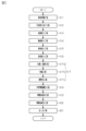
- the manufacturing method for electronic component 10 further includes a body preparation step S11, an R-chamfering processing step S12, a solvent introduction step S13, a catalyst introduction step S14, a body introduction step S15, a solution introduction step S16, a protective material formation step S17, an internal electrode exposure step S18, a conductor application step S19, a conductor hardening step S20, and a plating step S21.
- the element body preparation step S11 is performed.
- a rectangular parallelepiped element body 20 having six planes 22 is prepared. That is, the element body 20 at this stage is in a state before R-chamfering.
- a plurality of ceramic sheets that will become the element body 20 are prepared. The sheet is a thin plate. A conductive paste that will become the first internal electrode 41 is laminated on the sheet. A ceramic sheet that will become the element body 20 is laminated on the laminated paste. A conductive paste that will become the second internal electrode 42 is laminated on the sheet. In this manner, the ceramic sheet and the conductive paste are laminated. Then, by cutting to a predetermined size, the element body 20 is formed as an unfired laminate. After that, the unfired element body 20 is fired at a high temperature to prepare the element body 20.
- the ceramic sheet has a plurality of voids inside. Therefore, the prepared element body 20 has a plurality of voids 23 inside.
- the R-chamfering process S12 is performed.
- curved surfaces are formed at the boundary portions between two adjacent flat surfaces 22 and at the boundary portions between three adjacent flat surfaces 22 of the element body 20 prepared in the element body preparation process S11.
- the corners of the element body 20 are R-chamfered by barrel polishing to form curved surfaces at the above-mentioned boundary portions.
- a solvent introduction step S13 is performed as shown in Fig. 5.
- a solvent introduction step S13 2-propanol is introduced into a reaction vessel 81 as a solvent 82.
- a catalyst introduction step S14 is performed as shown in Fig. 5.
- stirring of the solvent 82 in the reaction vessel 81 is started.
- ammonia water is introduced into the reaction vessel 81 as an aqueous solution 83 containing a catalyst.
- the catalyst in this embodiment is a hydroxide ion, which functions as a catalyst for promoting hydrolysis of a metal alkoxide 84 described later.
- the element introduction step S15 is performed. As shown in FIG. 8, in the element introduction step S15, a plurality of element bodies 20 that have been formed in advance in the R chamfering step S12 as described above are introduced into a reaction vessel 81.
- a solution introduction step S16 is performed.
- a metal alkoxide 84 and a silane compound 85 are introduced into a reaction vessel 81.
- the metal alkoxide 84 is liquid tetraethyl orthosilicate (hereinafter referred to as "TEOS").
- TEOS is also called tetraethoxysilane.
- the silane compound 85 is liquid GPTMS.
- the GPTMS is introduced in a weight ratio of 0.12 or more and less than 1 relative to the TEOS. Specifically, the GPTMS is introduced in a weight ratio of approximately 0.43 relative to the TEOS.
- the amount of the solution containing the metal alkoxide 84 and the silane compound 85 to be added in the solution adding step S16 is calculated based on the porosity of the element body 20 and the area of the outer surface 21 of the element body 20 added in the element body adding step S15. Specifically, first, for each element body 20, the sum of the amount of the solution required to fill the voids 23 of the element body 20 and the amount of the solution required to form the film portion 51 covering the outer surface 21 of the element body 20 is calculated. The amount of the metal alkoxide 84 and the silane compound 85 required is calculated by multiplying this sum by the number of element bodies 20 added in the element body adding step S15.
- a protective material forming process S17 is performed.
- a protective material 50 is formed, which is made up of a filling portion 52 that fills the multiple voids 23 and a film portion 51 that covers the outer surface 21 of the base body 20.
- the protective material forming process S17 can be further divided into a filling/film forming process S17a, a drying process S17b, and a film hardening process S17c.
- the filling/film-forming step S17a is performed.
- the metal alkoxide 84 and the silane compound 85 are first put into the reaction vessel 81 by the solution-putting step S16, and then the stirring of the solvent 82 started in the above-mentioned solvent-putting step S13 is continued for a predetermined time.
- the metal alkoxide 84 is hydrolyzed by the hydroxide ions, which are the catalyst. Then, the condensation polymerization reaction between the metal alkoxides 84 proceeds more slowly than when the silane compound 85 is not present.
- the particles of the metal alkoxide 84 generated by the condensation polymerization reaction remain small in volume per molecule for a relatively long period of time. Therefore, the metal alkoxide 84 attached to the outer surface 21 of the element body 20 penetrates into the voids 23 inside the element body 20 together with the solution. After that, the condensation polymerization reaction of the metal alkoxide 84 proceeds in the voids 23, and the particles of the metal alkoxide 84 become larger. As a result, the filling portion 52 is formed in the voids 23. On the other hand, when the metal alkoxide 84 is hydrolyzed, the hydrolyzed metal alkoxide 84 and the silane compound 85 adhere to the outer surface 21 of the element body 20.
- the metal alkoxides 84 adhered to the outer surface 21 of the element body 20 are then condensed and polymerized together to form the film portion 51. Therefore, in the filling and film formation step S17a, the protective material 50 consisting of the sol-like film portion 51 and the sol-like filling portion 52 is formed by a liquid-phase reaction in the reaction vessel 81.
- a drying step S17b is performed.
- the element body 20 is removed from the reaction vessel 81 and dried.
- the sol-like protective material 50 is dried, and becomes a protective material 50 consisting of a gel-like film portion 51 and a gel-like filling portion 52.
- the film hardening step S17c is performed.
- the base body 20 on which the gel-like protective material 50 has been formed in the drying step S17b is baked at a temperature of 140 degrees or more and 160 degrees or less. Specifically, it is baked at a temperature of 150 degrees. This hardens the gel-like film portion 51 and the gel-like filling portion 52. In other words, the entire gel-like protective material 50 is hardened.
- the film portion 51 of the protective material 50 covers the entire outer surface 21 of the base body 20.
- the internal electrode exposure process S18 is performed.
- the film portion 51 covering the first end face 22A and the second end face 22B of the element body 20 is removed to expose the first internal electrode 41 and the second internal electrode 42.
- the film portion 51 is cut and removed by a laser from the entire area of the first end face 22A and the entire area of the second end face 22B of the element body 20.
- a conductor application step S19 is performed.
- a conductor paste is applied to a portion of the outer surface 21 of the element body 20 and a portion of the outer surface 53 of the film portion 51.
- the conductor paste is applied to two locations: the film portion 51 covering the first end face 22A of the element body 20 and a portion of the four side faces 22C of the element body 20 on the first positive direction X1 side, and the film portion 51 covering the second end face 22B of the element body 20 and a portion of the four side faces 22C of the element body 20 on the first negative direction X2 side.
- the conductor paste contains silver particles and an organic resin.
- the conductor hardening step S20 is performed.
- the base body 20 to which the conductor paste has been applied is heated to harden the conductor paste.
- the base body 20 is heated to about 200 degrees.
- the conductor paste applied in the conductor application step S19 is fired to form the first base electrode 61A and the second base electrode 62A.
- the plating process S21 is performed.
- a first metal layer 61B is formed on the surface of the first base electrode 61A by electroplating.
- a second metal layer 62B is formed on the surface of the second base electrode 62A.
- the first metal layer 61B and the second metal layer 62B are electroplated with two types of metal, nickel and tin, to form a two-layer structure. In this manner, the electronic component 10 is formed.
- the protective material 50 is glass containing a silane compound. Since this silane compound has a carbon chain with three or more carbon atoms, the glass easily enters the voids 23 inside the element body 20 during the manufacturing process of the protective material 50. As a result, the protective material 50 has not only a film portion 51 covering the outer surface 21 of the element body 20, but also a filling portion 52 filling the voids 23. In this way, if the filling portion 52, which is a part of the protective material 50, is filled into the voids 23 of the element body 20, it is possible to prevent cracks and the like from occurring in the element body 20 starting from the voids 23 in the element body 20.
- the thickness T of the film portion 51 is 20 nm or more and 1000 nm or less. If the thickness T of the film portion 51 is thinner than 20 nm, there is a risk that the adhesion between the film portion 51 and the first external electrode 61 and the second external electrode 62 may be insufficient. On the other hand, if the thickness T of the film portion 51 is greater than 1000 nm, the difference in temperature between the outer surface 53 of the film portion 51 and the surface of the film portion 51 facing the element body 20 may be large when the film portion 51 is fired. Therefore, there may be a difference in the degree of firing between the outer surface 53 of the film portion 51 and the surface of the film portion 51 facing the element body 20. Therefore, if the thickness T of the film portion 51 is 20 nm or more and 1000 nm or less, sufficient adhesion between the first external electrode 61 and the second external electrode 62 can be obtained, and uniform firing is also easy.
- the porosity is 0.5% or more and 2.5% or less. With this level of porosity, the manufacturing method of the above embodiment can fill almost all of the voids 23 with the filling portion 52 of the protective material 50. Therefore, no special process or special manufacturing equipment is required to form the filling portion 52 that fills the voids 23.
- the arithmetic mean roughness of the outer surface 53 of the film portion 51 is 6 nm or more and 100 nm or less. If the arithmetic mean roughness of the outer surface 53 of the film portion 51 is less than 6 nm, the anchor effect is unlikely to occur between the film portion 51 and the first external electrode 61 and the second external electrode 62, and there is a risk that sufficient adhesion cannot be obtained. On the other hand, if the arithmetic mean roughness of the outer surface 53 of the film portion 51 is greater than 100 nm, frictional forces are likely to occur on the outer surface 53 of the film portion 51, and there is a risk that damage due to friction may occur. Therefore, if the arithmetic mean roughness of the outer surface 53 of the film portion 51 is 6 nm or more and 100 nm or less, sufficient adhesion can be obtained and damage due to friction is unlikely to occur.
- the filling portion 52 fills the voids 23 that are located closest to the geometric center GC of the base body 20.
- the protective material 50 can be considered to fill almost all of the voids 23 in the base body 20. If the voids 23 are sufficiently filled in this way, the strength of the base body 20 can be reliably improved.
- the manufacturing method of electronic component 10 includes a solution introduction step S16 and a protective material formation step S17.
- a solution introduction step S16 By introducing metal alkoxide 84 and silane compound 85 having a carbon chain with three or more carbon atoms, film portion 51 and filling portion 52 can be formed. Therefore, the strength of element body 20 can be improved without making significant changes to the existing manufacturing method.
- the silane compound 85 has one or more functional groups selected from an epoxy group, a mercapto group, an amino group, a vinyl group, and a methacryl group. Silane compounds 85 having these functional groups are relatively easy to obtain and are also easy to produce. Therefore, they are easy to manufacture.
- GPTMS is introduced into the reaction vessel 81 in a weight ratio of 0.12 or more and less than 1 relative to TEOS.
- the protective material 50 can be easily formed while fully achieving the effect of slowing down the rate of the condensation polymerization reaction of TEOS.
- the manufacturing method of the electronic component 10 includes a conductor application step S19 and a conductor hardening step S20.
- the conductor paste contains resin as a material. Therefore, the first external electrode 61 and the second external electrode 62 contain resin. In other words, the first external electrode 61 and the second external electrode 62 are resin electrodes. Resin electrodes can be fired at a lower temperature than metal electrodes made of silver or the like. Therefore, the energy cost required for firing can be reduced.
- the material of the protective material 50 is a so-called organic-inorganic hybrid, so that high adhesion of each external electrode to the film portion 51 can be obtained.
- the filling portion 52 and the membrane portion 51 can be formed by firing at a temperature of 140 degrees or more and 160 degrees or less. This allows the use of a material that has a lower heat resistance than materials such as ceramics as the material for the element body 20. This increases the selectivity of the material for the element body 20. In addition, the energy cost required for firing can also be reduced.
- the electronic component 10 is not limited to a negative characteristic thermistor component.
- thermistor component other than a negative characteristic, or it may be a multilayer capacitor component or an inductor component.
- the material of the base body 20 is not limited to the example of the above embodiment.
- the material of the base body 20 is not limited to a sintered body, and can be any material that has voids inside.
- the material of the base body 20 may be a composite of resin and metal powder, fiber, thermosetting resin, etc.
- the shape of the element body 20 is not limited to the example of the above embodiment.
- the element body 20 may be a polygonal column shape other than a rectangular column shape having a central axis CA.
- the element body 20 may also be the core of a wire-wound inductor component.
- the core may have a so-called drum core shape.
- the core may have a cylindrical winding core portion and flange portions provided at each end of the winding core portion.
- the boundary portion between adjacent flat surfaces 22 of the outer surface 21 of the element body 20 does not have to be chamfered. In this case, no curved surface exists at the boundary portion.
- the first internal electrode 41 and the second internal electrode 42 may have any shape as long as they can ensure electrical conduction with the corresponding first external electrode 61 and second external electrode 62. Furthermore, the number of first internal electrodes 41 and second internal electrodes 42 does not matter, and the number of internal electrodes may be one, or three or more.
- the configuration of the first external electrode 61 is not limited to the example of the above embodiment.
- the first external electrode 61 may be composed of only the first base electrode 61A, and the first metal layer 61B may not have a two-layer structure. The same applies to the second external electrode 62.
- the materials of the first internal electrode 41, the second internal electrode 42, the first external electrode 61, and the second external electrode 62 are not important. It is sufficient to ensure electrical conduction between the first internal electrode 41 and the second internal electrode 42 and the corresponding first external electrode 61 and second external electrode 62.
- the material of the first internal electrode 41 and the second internal electrode 42 may be a conductive material such as silver or copper.
- the material of the first external electrode 61 and the second external electrode 62 does not have to be a resin electrode.
- it may be an electrode made of a mixture of silver and glass that does not contain resin.
- the material of the conductive filler mixed with the resin in the first external electrode 61 and the second external electrode 62 is not limited to silver. For example, it may be copper.
- the location of the first external electrode 61 is not limited to the example of the above embodiment.
- the first external electrode 61 may be disposed only on the first end surface 22A and one side surface 22C.
- the protective material 50 does not have to cover the entire area of the outer surface 21 of the element body 20.
- the area covered by the protective material 50 may be changed as appropriate depending on the shape of the element body 20, the positions of the first external electrode 61 and the second external electrode 62, etc.
- the glass contained in the protective material 50 may be diffused into the glass in the first base electrode 61A.
- the protective material 50 and the glass contained in the first base electrode 61A may be integrated.
- the second base electrode 62A may be integrated.
- the average thickness T of the film portion 51 may be less than 20 nm or more than 1000 nm. Regardless of the thickness T, the presence of the protective material 50 can improve the strength of the base body 20 compared to a case in which the protective material is not present.
- the arithmetic mean roughness of the outer surface 53 of the film portion 51 may be less than 6 nm or greater than 100 nm.
- the arithmetic mean roughness of the outer surface 53 of the film portion 51 can be changed as appropriate depending on the dimensions of the electronic component 10, the strength required of the electronic component 10, etc.
- equipment such as a laser microscope, an atomic force microscope, or a stylus profiling system may be used instead of white light interferometry.
- the filling portion 52 does not have to fill the void 23 closest to the geometric center GC of the base body 20. In other words, it is sufficient for the filling portion 52 to fill at least a portion of the void 23 of the base body 20.
- the filling rate may be less than 0.5% or more than 2.5%.
- the void rate may be less than 0.5% or more than 2.5%. Even if the void rate is small, as long as the filling portion 52 fills the voids 23, the effect of (1) can be obtained to some extent. Also, even if the void rate is large, it may be possible to fill all of the voids 23 with the filling portion 52, depending on the conditions of the solution introduction step S16 and the protective material formation step S17.
- the solvent 82 introduced in the solvent introduction step S13 is not limited to the example in the above embodiment, and may be any liquid capable of dispersing the metal alkoxide 84 appropriately.
- the solvent introduction step S13 may be performed after the catalyst introduction step S14 or the matrix introduction step S15.
- the solvent introduction step S13 may be performed prior to at least one of the solution introduction step S16 and the catalyst introduction step S14.
- the solvent introduction step S13 may also be omitted. In this case, for example, if the amount of water contained in the aqueous solution 83 containing the catalyst is appropriately large, the metal alkoxide 84 reacts in the liquid phase.
- the aqueous solution 83 containing the catalyst may also be introduced in a state where it is mixed with an organic solvent as the solvent 82.
- the aqueous solution 83 containing a catalyst is ammonia water, and the catalyst is hydroxide ions
- the catalyst is not limited to this. If the aqueous solution is basic, it can act as a catalyst to promote hydrolysis of the metal alkoxide 84, just like the ammonia water in the above embodiment. Even if the aqueous solution is acidic, it can act as a catalyst to promote hydrolysis of the metal alkoxide 84. Furthermore, even if the aqueous solution is neutral, it may contain a substance that functions as a catalyst, such as ions that can promote hydrolysis.
- a solid compound containing the catalyst and water may be added separately to the reaction vessel 81.
- the catalyst can be considered to have been added to the reaction vessel 81 when it is produced in the reaction vessel 81.
- a solid compound containing the catalyst may be added to the reaction vessel 81, and moisture in the air may be used as the water required for hydrolysis.
- the base body introduction step S15 may be performed prior to the catalyst introduction step S14. Also, if the base body introduction step S15 is performed prior to the catalyst introduction step S14, the solution introduction step S16 may be performed prior to the catalyst introduction step S14 or the base body introduction step S15. At the very least, the base body introduction step S15 needs to be performed prior to either the solution introduction step S16 or the catalyst introduction step S14.
- a solution containing a precursor for generating the metal alkoxide 84 may be added instead of the metal alkoxide 84.
- a metal complex or acetate which is a metal alkoxide precursor, may be added.
- Examples of the metal complex include acetylacetonates such as lithium acetylacetonate, titanium (IV) oxyacetylacetonate, titanium diisopropoxide bis(acetylacetonate), zirconium (IV) trifluoroacetylacetonate, zirconium (IV) acetylacetonate, aluminum acetylacetonate, aluminum (III) acetylacetonate, calcium (II) acetylacetonate, and zinc (II) acetylacetonate.
- Examples of the acetate include zirconium acetate, zirconium (IV) hydroxide acetate, and basic aluminum acetate.
- the metal alkoxide 84 may be generated inside the reaction vessel 81 instead of being introduced into the reaction vessel 81 after generating the metal alkoxide 84 outside the reaction vessel 81.
- the metal alkoxide 84 is generated by reacting a metal salt with an alcohol. Therefore, when a metal salt and an alcohol, which are metal alkoxide precursors, are introduced into the reaction vessel 81 and react with each other to generate the metal alkoxide 84, the metal alkoxide 84 can be considered to have been introduced into the reaction vessel 81.
- Metal alkoxide 84 is not limited to TEOS.
- the metal contained in metal alkoxide 84 may be titanium, zirconium, aluminum, or the like. If the metal contained in metal alkoxide 84 is silicon, the reaction rate is slower than other metals, and it is easier to control the reaction rate of metal alkoxide 84 to a constant value.
- the alkoxy group of metal alkoxide 84 may be a methoxy group, a propoxy group, or the like, or may be modified with a functional group such as a long-chain alkyl group or an epoxy group as in a coupling agent.
- the coordination number for the metal contained in metal alkoxide 84 is not limited to 4-coordination, and may be 3-coordination or 2-coordination.
- Silane compound 85 is not limited to GPTMS as long as it has a carbon chain with 3 or more carbon atoms. Silane compound 85 may not have any of epoxy groups, mercapto groups, amino groups, vinyl groups, or methacryl groups.
- silane compound 85 may be a silane compound such as 3-aminopropyltrimethoxysilane, 3-aminopropyltriethoxysilane, 3-(2-aminoethyl)aminopropyltrimethoxysilane, 3-phenylaminopropyltrimethoxysilane, (3-glycidoxypropyl)methyldimethoxysilane, 3-methacryloxypropyltrimethoxysilane, 3-methacryloxypropylmethyldimethoxysilane, 3-mercaptopropyltrimethoxysilane, n-propyltrimethoxysilane, isobutyltrimethoxysilane, n-hexyltrimethoxys
- the protective material 50 that has undergone the protective material formation process S17 contains a silane compound 85.
- the order in which the metal alkoxide 84 and the silane compound 85 are introduced does not matter. Also, a solution in which the metal alkoxide 84 and the silane compound 85 are mixed in a predetermined ratio may be introduced into the reaction vessel 81.
- the weight ratio of the silane compound 85 to the metal alkoxide 84 introduced into the reaction vessel 81 may be less than 0.12 or may be 1 or more. If the protective material 50 can be formed, the strength of the base body 20 can be improved.
- protective material 50 can be formed in protective material forming process S17, film hardening process S17c does not have to be performed after drying process S17b.
- protective material 50 may be hardened in conjunction with firing the conductor paste in conductor hardening process S20. In that case, conductor hardening process S20 and film hardening process S17c are considered to be performed simultaneously.
- the firing temperature of the solution containing the metal alkoxide 84 and the silane compound 85 attached to the outer surface 21 of the base body 20 may be lower than 140 degrees or higher than 160 degrees. Even if the firing temperature is high, the protective material 50 can be formed by using a highly heat-resistant material such as ceramics as the material of the base body 20.
- the method for removing the film portion 51 is not limited to laser cutting.
- the first internal electrode 41 and the second internal electrode 42 may be exposed using methods such as ion milling and polishing.
- the range in which the film portion 51 is removed is not limited to the example of the above embodiment.
- the conductor hardening step S20 is not limited to heating the conductor paste.
- ultraviolet light may be irradiated.
- the material of the conductive paste is not limited to resin. If the arithmetic mean roughness of the area where the conductive paste is applied is large, adhesion due to the anchor effect can be obtained.
- a protective material covering all or part of an outer surface of the element body; and an external electrode covering a part of the outer surface of the protective material;
- the element body has a plurality of voids therein,
- the protective material is glass containing a silane compound having a carbon chain with three or more carbon atoms, and the electronic component has a filling portion that fills at least a portion of the voids, and a film portion that covers the outer surface of the body.
- an element preparation step of preparing an element having a plurality of voids therein an element introduction step of introducing the element into a reaction vessel; a solution introduction step of introducing a solution containing a metal alkoxide or a metal alkoxide precursor and a silane compound having a carbon chain having 3 or more carbon atoms into the reaction vessel; and a protective material formation process for hydrolyzing and condensation polymerizing the metal alkoxide on the outer surface of the element body, and forming a protective material consisting of a filling portion that fills the multiple voids and a film portion that covers the outer surface of the element body.
- the silane compound has one or more functional groups selected from an epoxy group, a mercapto group, an amino group, a vinyl group, and a methacryl group.
- the metal alkoxide is tetraethyl orthosilicate;
- the silane compound is 3-glycidoxypropyltrimethoxysilane,
Landscapes
- Engineering & Computer Science (AREA)
- Microelectronics & Electronic Packaging (AREA)
- Power Engineering (AREA)
- Manufacturing & Machinery (AREA)
- Chemical & Material Sciences (AREA)
- Electromagnetism (AREA)
- Physics & Mathematics (AREA)
- Materials Engineering (AREA)
- Organic Chemistry (AREA)
- Geochemistry & Mineralogy (AREA)
- General Chemical & Material Sciences (AREA)
- Chemical Kinetics & Catalysis (AREA)
- Life Sciences & Earth Sciences (AREA)
- Fixed Capacitors And Capacitor Manufacturing Machines (AREA)
- Ceramic Capacitors (AREA)
- Thermistors And Varistors (AREA)
Priority Applications (3)
| Application Number | Priority Date | Filing Date | Title |
|---|---|---|---|
| JP2024572826A JPWO2024157505A1 (https=) | 2023-01-27 | 2023-08-23 | |
| CN202380018982.4A CN118715578A (zh) | 2023-01-27 | 2023-08-23 | 电子部件和电子部件的制造方法 |
| US18/983,399 US20250118461A1 (en) | 2023-01-27 | 2024-12-17 | Electronic component and method for manufacturing electronic component |
Applications Claiming Priority (2)
| Application Number | Priority Date | Filing Date | Title |
|---|---|---|---|
| JP2023011007 | 2023-01-27 | ||
| JP2023-011007 | 2023-01-27 |
Related Child Applications (1)
| Application Number | Title | Priority Date | Filing Date |
|---|---|---|---|
| US18/983,399 Continuation US20250118461A1 (en) | 2023-01-27 | 2024-12-17 | Electronic component and method for manufacturing electronic component |
Publications (1)
| Publication Number | Publication Date |
|---|---|
| WO2024157505A1 true WO2024157505A1 (ja) | 2024-08-02 |
Family
ID=91970199
Family Applications (1)
| Application Number | Title | Priority Date | Filing Date |
|---|---|---|---|
| PCT/JP2023/030254 Ceased WO2024157505A1 (ja) | 2023-01-27 | 2023-08-23 | 電子部品及び電子部品の製造方法 |
Country Status (4)
| Country | Link |
|---|---|
| US (1) | US20250118461A1 (https=) |
| JP (1) | JPWO2024157505A1 (https=) |
| CN (1) | CN118715578A (https=) |
| WO (1) | WO2024157505A1 (https=) |
Citations (7)
| Publication number | Priority date | Publication date | Assignee | Title |
|---|---|---|---|---|
| JPH04282802A (ja) * | 1991-03-11 | 1992-10-07 | Taiyo Yuden Co Ltd | セラミック電子部品の製造法 |
| JPH0897008A (ja) * | 1994-02-21 | 1996-04-12 | Matsushita Electric Ind Co Ltd | バリスタの製造法 |
| JP2003197406A (ja) * | 2001-12-25 | 2003-07-11 | Maruwa Co Ltd | チップ型バリスタの製造方法 |
| US20160042864A1 (en) * | 2014-08-05 | 2016-02-11 | Samsung Electro-Mechanics Co., Ltd. | Multilayer ceramic capacitor |
| JP2017147336A (ja) * | 2016-02-17 | 2017-08-24 | 株式会社村田製作所 | 着色膜の形成方法 |
| JP2021019002A (ja) * | 2019-07-17 | 2021-02-15 | 三菱マテリアル株式会社 | 電子部品の製造方法 |
| JP2021027163A (ja) * | 2019-08-05 | 2021-02-22 | 三菱マテリアル株式会社 | 保護膜付きサーミスタおよびその製造方法 |
-
2023
- 2023-08-23 WO PCT/JP2023/030254 patent/WO2024157505A1/ja not_active Ceased
- 2023-08-23 JP JP2024572826A patent/JPWO2024157505A1/ja active Pending
- 2023-08-23 CN CN202380018982.4A patent/CN118715578A/zh active Pending
-
2024
- 2024-12-17 US US18/983,399 patent/US20250118461A1/en active Pending
Patent Citations (7)
| Publication number | Priority date | Publication date | Assignee | Title |
|---|---|---|---|---|
| JPH04282802A (ja) * | 1991-03-11 | 1992-10-07 | Taiyo Yuden Co Ltd | セラミック電子部品の製造法 |
| JPH0897008A (ja) * | 1994-02-21 | 1996-04-12 | Matsushita Electric Ind Co Ltd | バリスタの製造法 |
| JP2003197406A (ja) * | 2001-12-25 | 2003-07-11 | Maruwa Co Ltd | チップ型バリスタの製造方法 |
| US20160042864A1 (en) * | 2014-08-05 | 2016-02-11 | Samsung Electro-Mechanics Co., Ltd. | Multilayer ceramic capacitor |
| JP2017147336A (ja) * | 2016-02-17 | 2017-08-24 | 株式会社村田製作所 | 着色膜の形成方法 |
| JP2021019002A (ja) * | 2019-07-17 | 2021-02-15 | 三菱マテリアル株式会社 | 電子部品の製造方法 |
| JP2021027163A (ja) * | 2019-08-05 | 2021-02-22 | 三菱マテリアル株式会社 | 保護膜付きサーミスタおよびその製造方法 |
Also Published As
| Publication number | Publication date |
|---|---|
| CN118715578A (zh) | 2024-09-27 |
| JPWO2024157505A1 (https=) | 2024-08-02 |
| US20250118461A1 (en) | 2025-04-10 |
Similar Documents
| Publication | Publication Date | Title |
|---|---|---|
| JP2022014533A (ja) | 電子部品 | |
| JP2022014536A (ja) | 電子部品 | |
| WO2006126333A1 (ja) | 積層セラミック電子部品およびその製造方法 | |
| WO2025004432A1 (ja) | 電子部品 | |
| US20250232899A1 (en) | Electronic component and film forming method | |
| JP2022014532A (ja) | 電子部品及び電子部品の製造方法 | |
| JP7593431B2 (ja) | 成膜方法及び電子部品の製造方法 | |
| WO2024157505A1 (ja) | 電子部品及び電子部品の製造方法 | |
| JP2022014534A (ja) | 電子部品 | |
| JP2022014535A (ja) | 電子部品 | |
| US20250266189A1 (en) | Protective glass film | |
| WO2024034425A1 (ja) | 電子部品及び電子部品の製造方法 | |
| JP7582508B2 (ja) | 電子部品 | |
| JP2016063079A (ja) | 抵抗素子およびその製造方法 | |
| WO2022264637A1 (ja) | 電子部品 | |
| CN113939476B (zh) | 钛酸钡粒子、其制造方法及钛酸钡粒子的分散液 | |
| WO2023084878A1 (ja) | 電子部品 | |
| JP7658455B2 (ja) | 電子部品 | |
| WO2025115910A1 (ja) | 電子部品及び電子部品の製造方法 | |
| JP2023168785A (ja) | 電子部品への熱負荷の測定方法 | |
| WO2024029252A1 (ja) | 電子部品 | |
| WO2025089298A1 (ja) | 電子部品、保護膜の成膜方法、及び電子部品の製造方法 | |
| JP6544485B2 (ja) | セラミック電子部品及びセラミック電子部品の製造方法 | |
| WO2024048037A1 (ja) | 電子部品及び成膜方法 | |
| WO2024262064A1 (ja) | 電子部品 |
Legal Events
| Date | Code | Title | Description |
|---|---|---|---|
| WWE | Wipo information: entry into national phase |
Ref document number: 202380018982.4 Country of ref document: CN |
|
| 121 | Ep: the epo has been informed by wipo that ep was designated in this application |
Ref document number: 23918465 Country of ref document: EP Kind code of ref document: A1 |
|
| ENP | Entry into the national phase |
Ref document number: 2024572826 Country of ref document: JP Kind code of ref document: A |
|
| WWE | Wipo information: entry into national phase |
Ref document number: 2024572826 Country of ref document: JP |
|
| NENP | Non-entry into the national phase |
Ref country code: DE |
|
| 122 | Ep: pct application non-entry in european phase |
Ref document number: 23918465 Country of ref document: EP Kind code of ref document: A1 |