WO2024143378A1 - SiC半導体装置 - Google Patents
SiC半導体装置 Download PDFInfo
- Publication number
- WO2024143378A1 WO2024143378A1 PCT/JP2023/046699 JP2023046699W WO2024143378A1 WO 2024143378 A1 WO2024143378 A1 WO 2024143378A1 JP 2023046699 W JP2023046699 W JP 2023046699W WO 2024143378 A1 WO2024143378 A1 WO 2024143378A1
- Authority
- WO
- WIPO (PCT)
- Prior art keywords
- planar
- electrode
- insulating film
- region
- drift
- Prior art date
- Legal status (The legal status is an assumption and is not a legal conclusion. Google has not performed a legal analysis and makes no representation as to the accuracy of the status listed.)
- Ceased
Links
Images











Classifications
-
- H—ELECTRICITY
- H10—SEMICONDUCTOR DEVICES; ELECTRIC SOLID-STATE DEVICES NOT OTHERWISE PROVIDED FOR
- H10D—INORGANIC ELECTRIC SEMICONDUCTOR DEVICES
- H10D30/00—Field-effect transistors [FET]
- H10D30/60—Insulated-gate field-effect transistors [IGFET]
- H10D30/64—Double-diffused metal-oxide semiconductor [DMOS] FETs
- H10D30/66—Vertical DMOS [VDMOS] FETs
-
- H—ELECTRICITY
- H10—SEMICONDUCTOR DEVICES; ELECTRIC SOLID-STATE DEVICES NOT OTHERWISE PROVIDED FOR
- H10D—INORGANIC ELECTRIC SEMICONDUCTOR DEVICES
- H10D62/00—Semiconductor bodies, or regions thereof, of devices having potential barriers
- H10D62/10—Shapes, relative sizes or dispositions of the regions of the semiconductor bodies; Shapes of the semiconductor bodies
- H10D62/124—Shapes, relative sizes or dispositions of the regions of semiconductor bodies or of junctions between the regions
- H10D62/126—Top-view geometrical layouts of the regions or the junctions
- H10D62/127—Top-view geometrical layouts of the regions or the junctions of cellular field-effect devices, e.g. multicellular DMOS transistors or IGBTs
-
- H—ELECTRICITY
- H10—SEMICONDUCTOR DEVICES; ELECTRIC SOLID-STATE DEVICES NOT OTHERWISE PROVIDED FOR
- H10D—INORGANIC ELECTRIC SEMICONDUCTOR DEVICES
- H10D62/00—Semiconductor bodies, or regions thereof, of devices having potential barriers
- H10D62/80—Semiconductor bodies, or regions thereof, of devices having potential barriers characterised by the materials
- H10D62/83—Semiconductor bodies, or regions thereof, of devices having potential barriers characterised by the materials being Group IV materials, e.g. B-doped Si or undoped Ge
- H10D62/832—Semiconductor bodies, or regions thereof, of devices having potential barriers characterised by the materials being Group IV materials, e.g. B-doped Si or undoped Ge being Group IV materials comprising two or more elements, e.g. SiGe
- H10D62/8325—Silicon carbide
-
- H—ELECTRICITY
- H10—SEMICONDUCTOR DEVICES; ELECTRIC SOLID-STATE DEVICES NOT OTHERWISE PROVIDED FOR
- H10D—INORGANIC ELECTRIC SEMICONDUCTOR DEVICES
- H10D64/00—Electrodes of devices having potential barriers
- H10D64/111—Field plates
-
- H—ELECTRICITY
- H10—SEMICONDUCTOR DEVICES; ELECTRIC SOLID-STATE DEVICES NOT OTHERWISE PROVIDED FOR
- H10D—INORGANIC ELECTRIC SEMICONDUCTOR DEVICES
- H10D64/00—Electrodes of devices having potential barriers
- H10D64/20—Electrodes characterised by their shapes, relative sizes or dispositions
- H10D64/23—Electrodes carrying the current to be rectified, amplified, oscillated or switched, e.g. sources, drains, anodes or cathodes
- H10D64/251—Source or drain electrodes for field-effect devices
- H10D64/252—Source or drain electrodes for field-effect devices for vertical or pseudo-vertical devices
-
- H—ELECTRICITY
- H10—SEMICONDUCTOR DEVICES; ELECTRIC SOLID-STATE DEVICES NOT OTHERWISE PROVIDED FOR
- H10D—INORGANIC ELECTRIC SEMICONDUCTOR DEVICES
- H10D64/00—Electrodes of devices having potential barriers
- H10D64/20—Electrodes characterised by their shapes, relative sizes or dispositions
- H10D64/23—Electrodes carrying the current to be rectified, amplified, oscillated or switched, e.g. sources, drains, anodes or cathodes
- H10D64/251—Source or drain electrodes for field-effect devices
- H10D64/252—Source or drain electrodes for field-effect devices for vertical or pseudo-vertical devices
- H10D64/2527—Source or drain electrodes for field-effect devices for vertical or pseudo-vertical devices for vertical devices wherein the source or drain electrodes are recessed in semiconductor bodies
-
- H—ELECTRICITY
- H10—SEMICONDUCTOR DEVICES; ELECTRIC SOLID-STATE DEVICES NOT OTHERWISE PROVIDED FOR
- H10D—INORGANIC ELECTRIC SEMICONDUCTOR DEVICES
- H10D64/00—Electrodes of devices having potential barriers
- H10D64/20—Electrodes characterised by their shapes, relative sizes or dispositions
- H10D64/23—Electrodes carrying the current to be rectified, amplified, oscillated or switched, e.g. sources, drains, anodes or cathodes
- H10D64/251—Source or drain electrodes for field-effect devices
- H10D64/258—Source or drain electrodes for field-effect devices characterised by the relative positions of the source or drain electrodes with respect to the gate electrode
-
- H—ELECTRICITY
- H10—SEMICONDUCTOR DEVICES; ELECTRIC SOLID-STATE DEVICES NOT OTHERWISE PROVIDED FOR
- H10D—INORGANIC ELECTRIC SEMICONDUCTOR DEVICES
- H10D64/00—Electrodes of devices having potential barriers
- H10D64/20—Electrodes characterised by their shapes, relative sizes or dispositions
- H10D64/27—Electrodes not carrying the current to be rectified, amplified, oscillated or switched, e.g. gates
- H10D64/311—Gate electrodes for field-effect devices
- H10D64/411—Gate electrodes for field-effect devices for FETs
- H10D64/511—Gate electrodes for field-effect devices for FETs for IGFETs
- H10D64/512—Disposition of the gate electrodes, e.g. buried gates
-
- H—ELECTRICITY
- H10—SEMICONDUCTOR DEVICES; ELECTRIC SOLID-STATE DEVICES NOT OTHERWISE PROVIDED FOR
- H10D—INORGANIC ELECTRIC SEMICONDUCTOR DEVICES
- H10D64/00—Electrodes of devices having potential barriers
- H10D64/20—Electrodes characterised by their shapes, relative sizes or dispositions
- H10D64/27—Electrodes not carrying the current to be rectified, amplified, oscillated or switched, e.g. gates
- H10D64/311—Gate electrodes for field-effect devices
- H10D64/411—Gate electrodes for field-effect devices for FETs
- H10D64/511—Gate electrodes for field-effect devices for FETs for IGFETs
- H10D64/514—Gate electrodes for field-effect devices for FETs for IGFETs characterised by the insulating layers
-
- H—ELECTRICITY
- H10—SEMICONDUCTOR DEVICES; ELECTRIC SOLID-STATE DEVICES NOT OTHERWISE PROVIDED FOR
- H10D—INORGANIC ELECTRIC SEMICONDUCTOR DEVICES
- H10D64/00—Electrodes of devices having potential barriers
- H10D64/20—Electrodes characterised by their shapes, relative sizes or dispositions
- H10D64/27—Electrodes not carrying the current to be rectified, amplified, oscillated or switched, e.g. gates
- H10D64/311—Gate electrodes for field-effect devices
- H10D64/411—Gate electrodes for field-effect devices for FETs
- H10D64/511—Gate electrodes for field-effect devices for FETs for IGFETs
- H10D64/517—Gate electrodes for field-effect devices for FETs for IGFETs characterised by the conducting layers
- H10D64/519—Gate electrodes for field-effect devices for FETs for IGFETs characterised by the conducting layers characterised by their top-view geometrical layouts
-
- H—ELECTRICITY
- H10—SEMICONDUCTOR DEVICES; ELECTRIC SOLID-STATE DEVICES NOT OTHERWISE PROVIDED FOR
- H10D—INORGANIC ELECTRIC SEMICONDUCTOR DEVICES
- H10D12/00—Bipolar devices controlled by the field effect, e.g. insulated-gate bipolar transistors [IGBT]
- H10D12/01—Manufacture or treatment
- H10D12/031—Manufacture or treatment of IGBTs
- H10D12/032—Manufacture or treatment of IGBTs of vertical IGBTs
-
- H—ELECTRICITY
- H10—SEMICONDUCTOR DEVICES; ELECTRIC SOLID-STATE DEVICES NOT OTHERWISE PROVIDED FOR
- H10D—INORGANIC ELECTRIC SEMICONDUCTOR DEVICES
- H10D12/00—Bipolar devices controlled by the field effect, e.g. insulated-gate bipolar transistors [IGBT]
- H10D12/01—Manufacture or treatment
- H10D12/031—Manufacture or treatment of IGBTs
- H10D12/032—Manufacture or treatment of IGBTs of vertical IGBTs
- H10D12/038—Manufacture or treatment of IGBTs of vertical IGBTs having a recessed gate, e.g. trench-gate IGBTs
-
- H—ELECTRICITY
- H10—SEMICONDUCTOR DEVICES; ELECTRIC SOLID-STATE DEVICES NOT OTHERWISE PROVIDED FOR
- H10D—INORGANIC ELECTRIC SEMICONDUCTOR DEVICES
- H10D12/00—Bipolar devices controlled by the field effect, e.g. insulated-gate bipolar transistors [IGBT]
- H10D12/411—Insulated-gate bipolar transistors [IGBT]
- H10D12/415—Insulated-gate bipolar transistors [IGBT] having edge termination structures
-
- H—ELECTRICITY
- H10—SEMICONDUCTOR DEVICES; ELECTRIC SOLID-STATE DEVICES NOT OTHERWISE PROVIDED FOR
- H10D—INORGANIC ELECTRIC SEMICONDUCTOR DEVICES
- H10D12/00—Bipolar devices controlled by the field effect, e.g. insulated-gate bipolar transistors [IGBT]
- H10D12/411—Insulated-gate bipolar transistors [IGBT]
- H10D12/441—Vertical IGBTs
-
- H—ELECTRICITY
- H10—SEMICONDUCTOR DEVICES; ELECTRIC SOLID-STATE DEVICES NOT OTHERWISE PROVIDED FOR
- H10D—INORGANIC ELECTRIC SEMICONDUCTOR DEVICES
- H10D12/00—Bipolar devices controlled by the field effect, e.g. insulated-gate bipolar transistors [IGBT]
- H10D12/411—Insulated-gate bipolar transistors [IGBT]
- H10D12/441—Vertical IGBTs
- H10D12/461—Vertical IGBTs having non-planar surfaces, e.g. having trenches, recesses or pillars in the surfaces of the emitter, base or collector regions
- H10D12/481—Vertical IGBTs having non-planar surfaces, e.g. having trenches, recesses or pillars in the surfaces of the emitter, base or collector regions having gate structures on slanted surfaces, on vertical surfaces, or in grooves, e.g. trench gate IGBTs
Definitions
- the present disclosure provides a novel SiC semiconductor device.
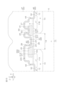
- the present disclosure provides a SiC semiconductor device including: a SiC chip having a principal surface; a channel region formed in a surface portion of the principal surface; a drift region adjacent to the channel region in the surface portion of the principal surface; a gate insulating film formed on the principal surface and having a channel covering portion covering the channel region and a drift covering portion covering the drift region; a planar gate electrode disposed on the channel covering portion and facing the channel region via the channel covering portion in the vertical direction; and a planar source electrode disposed on the drift covering portion at a distance from the planar gate electrode so as to face the planar gate electrode in the horizontal direction and facing the drift region via the drift covering portion in the vertical direction.
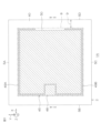
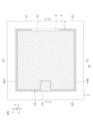
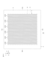
- FIG. 1 is a plan view showing a semiconductor device according to a first embodiment.
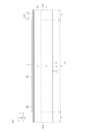
- FIG. 2 is a cross-sectional view taken along the line II-II shown in FIG.
- FIG. 3 is a plan view showing an example of the layout of the chip shown in FIG.
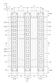
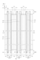
- FIG. 4 is an enlarged plan view showing an example of the layout of active regions together with a first planar structure according to the first embodiment.
- FIG. 5 is a cross-sectional view taken along line V-V shown in FIG.
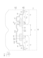
- FIG. 6 is an enlarged cross-sectional view showing a first planar structure according to the first embodiment.
- FIG. 7A is an enlarged cross-sectional view showing a first planar structure according to the second embodiment.
- FIG. 7B is an enlarged cross-sectional view showing the first planar structure according to the third embodiment.
- FIG. 7C is an enlarged cross-sectional view showing the first planar structure according to the fourth embodiment.
- FIG. 7D is an enlarged cross-sectional view showing the first planar structure according to the fifth embodiment.
- FIG. 7E is an enlarged cross-sectional view showing the first planar structure according to the sixth embodiment.
- FIG. 7F is an enlarged cross-sectional view showing the first planar structure according to the seventh embodiment.
- FIG. 7G is an enlarged plan view showing the first planar structure according to the eighth embodiment.
- FIG. 7H is an enlarged plan view showing the first planar structure according to the ninth embodiment.
- FIG. 7I is an enlarged plan view showing a first planar structure according to a tenth embodiment.
- FIG. 7J is an enlarged cross-sectional view showing the first planar structure according to the eleventh embodiment.
- FIG. 8 is a plan view showing a semiconductor device according to the second embodiment.
- FIG. 9 is a cross-sectional view taken along line IX-IX shown in FIG.
- FIG. 10 is a plan view showing an example of the layout of the chip shown in FIG.
- FIG. 11 is an enlarged plan view showing an example of the layout of an active region together with the second planar structure according to the first embodiment.
- FIG. 12 is a cross-sectional view taken along the line XII-XII shown in FIG.
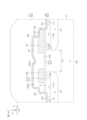
- FIG. 13 is an enlarged cross-sectional view showing the second planar structure.
- FIG. 14A is an enlarged cross-sectional view showing a second planar structure according to the second embodiment.
- FIG. 14B is an enlarged cross-sectional view showing a second planar structure according to the third embodiment.
- FIG. 14C is an enlarged cross-sectional view showing a second planar structure according to the fourth embodiment.
- FIG. 14D is an enlarged cross-sectional view showing a second planar structure according to the fifth embodiment.
- FIG. 14E is an enlarged cross-sectional view showing a second planar structure according to the sixth embodiment.
- FIG. 15 is an enlarged cross-sectional view showing a main part of a semiconductor device according to the third embodiment.
- FIG. 16 is an enlarged plan view showing an example of the layout of an active region of a semiconductor device according to the fourth embodiment.
- this term includes a numerical value (shape) that is equal to the numerical value (shape) of the comparison target, as well as a numerical error (shape error) within a range of ⁇ 10% based on the numerical value (shape) of the comparison target.
- shape a numerical value that is equal to the numerical value (shape) of the comparison target
- error a numerical error within a range of ⁇ 10% based on the numerical value (shape) of the comparison target.
- the off-direction is preferably the a-axis direction of the SiC single crystal (i.e., the second direction Y).
- the off-angle may be greater than 0° and less than or equal to 10°.
- the off-angle may have a value that falls within any one of the following ranges: greater than 0° and less than or equal to 1°, 1° or more and less than or equal to 2.5°, 2.5° or more and less than or equal to 5°, 5° or more and less than or equal to 7.5°, and 7.5° or more and less than or equal to 10°.
- the SiC semiconductor device 1A includes a plurality of p-type channel regions 13A, 13B formed in the surface layer portion of the first main surface 3.
- the plurality of channel regions 13A, 13B are partitioned in the surface layer portion of the plurality of body regions 10 into regions between the peripheries of the plurality of body regions 10 and the peripheries of the plurality of source regions 11A, 11B.
- the multiple surface drift regions 14 are arranged at intervals in the first direction X, and are each formed in a strip extending in the second direction Y.
- the multiple surface drift regions 14 are arranged at intervals in the m-axis direction of the SiC single crystal, and extend in the a-axis direction of the SiC single crystal.
- the multiple surface drift regions 14 are also formed in stripes extending in the second direction Y (a-axis direction).
- the first channel covering portion 21A partially covers the first source region 11A at a distance from the contact region 12, exposing a part of the first source region 11A and the contact region 12 from the first main surface 3.
- the second channel covering portion 21B partially covers the second source region 11B at a distance from the contact region 12, exposing a part of the second source region 11B and the contact region 12 from the first main surface 3.
- the drift covering portion 21C is continuous with the first channel covering portion 21A and the second channel covering portion 21B.
- the planar insulating film 27 has a portion extending horizontally in a film-like manner along the first channel covering portion 21A, a portion extending horizontally in a film-like manner along the second channel covering portion 21B, a portion extending horizontally in a film-like manner along the first electrode portion 22A, and a portion extending horizontally in a film-like manner along the second electrode portion 22B.
- the portions of the planar insulating film 27 that cover the first electrode portion 22A and the second electrode portion 22B are positioned above the portions of the planar insulating film 27 that cover the first channel covering portion 21A and the second channel covering portion 21B.
- the planar insulating film 27 is connected to the isolation insulating film 25 at the inner part of the planar gate electrode 22, and defines a recess through-hole 28 that communicates with the insulating recess 26.
- the recess through-hole 28 is formed in a band shape extending along the insulating recess 26 in a plan view. In this embodiment, the recess through-hole 28 is formed narrower than the surface drift region 14 in a cross-sectional view.
- the first planar structures 20A each include a planar source electrode 29 arranged on the gate insulating film 21.
- the planar source electrode 29 is arranged on the drift coating portion 21C at a distance from the planar gate electrode 22 so as to face the planar gate electrode 22 in the horizontal direction, and faces the surface drift region 14 via the drift coating portion 21C in the vertical direction Z.
- the planar source electrode 29 is disposed in the insulating recess 26.
- the planar source electrode 29 is formed in a strip shape extending in the second direction Y along the insulating recess 26 in a plan view.
- the planar source electrode 29 extends in the a-axis direction of the SiC single crystal.
- the extension direction of the planar source electrode 29 coincides with the off-direction of the SiC single crystal.
- the planar source electrode 29 is capacitively coupled to the surface drift region 14 via the gate insulating film 21. Specifically, the planar source electrode 29 is capacitively coupled to the surface drift region 14 via the intermediate insulating film 24 and the gate insulating film 21.
- the planar gate electrode 22 and the planar source electrode 29 are arranged horizontally adjacent to each other on the same gate insulating film 21, and the planar source electrode 29 faces the surface drift region 14 via the gate insulating film 21. Therefore, the source potential occurs near the side of the planar gate electrode 22, reducing the electrical effect of the gate potential on the surface drift region 14. This prevents the planar gate electrode 22 from being capacitively coupled to the surface drift region 14 via the gate insulating film 21.
- the planar source electrode 29 includes a conductive material different from that of the planar gate electrode 22. Specifically, the planar source electrode 29 includes a metal. More specifically, the planar source electrode 29 includes a metallic underlying electrode film 30 and a metallic electrode body 31.
- the underlying electrode film 30 is made of a metal barrier film.
- the underlying electrode film 30 includes at least one of a Ti film, a TiN film, and a W film.
- the underlying electrode film 30 includes a Ti film.
- the underlying electrode film 30 is formed in the form of a film along the wall surfaces of the insulating recess 26 and the wall surfaces of the recess through-hole 28.
- the underlying electrode film 30 covers the intermediate insulating film 24 and the isolation insulating film 25 within the insulating recess 26.
- the underlying electrode film 30 covers the planar insulating film 27 within the recess through-hole 28.
- the underlying electrode film 30 has a thickness less than 1/2 the width of the insulating recess 26, and defines an electrode recess within the insulating recess 26 and the recess through-hole 28.
- the electrode body 31 forms the body of the planar source electrode 29.
- the electrode body 31 includes at least one of a pure W film (a W film having a purity of 99% or more), a W alloy film, an Al film, a Cu film, an Al alloy film, and a Cu alloy film.
- the electrode body 31 may include at least one of a pure Cu film (a Cu film having a purity of 99% or more), a pure Al film (an Al film having a purity of 99% or more), an AlCu alloy film, an AlSi alloy film, and an AlSiCu alloy film.
- the electrode body 31 includes an Al alloy film (an AlSiCu alloy film in this embodiment).
- the SiC semiconductor device 1A includes a plurality of contact recesses 32 formed in the regions between adjacent first planar structures 20A (a plurality of planar insulating films 27) on the first main surface 3.
- the plurality of contact recesses 32 are arranged at intervals in the first direction X and are each formed in a strip shape extending in the second direction Y.
- Each contact recess 32 extends from the contact region 12 toward the periphery of the body region 10, partially exposing both the first source region 11A and the second source region 11B from both sides.
- the bottom wall of each contact recess 32 is formed at a distance from the bottom of the first source region 11A and the bottom of the second source region 11B toward the first main surface 3. It is not necessary for the contact recess 32 to be formed, and a configuration without the contact recess 32 may be adopted.
- the SiC semiconductor device 1A includes an interlayer insulating film 40 that selectively covers the first main surface 3.
- the interlayer insulating film 40 has a laminated structure including a first insulating film 41 and a second insulating film 42.
- the first insulating film 41 may include at least one of a silicon oxide film, a silicon nitride film, and a silicon oxynitride film. It is particularly preferable that the first insulating film 41 includes a silicon oxide film made of an oxide of the chip 2.
- the first insulating film 41 selectively covers the first main surface 3 in the active region 8 and the peripheral region 9. Specifically, the first insulating film 41 covers the region outside the multiple gate insulating films 21 in the active region 8, and is connected to the multiple gate insulating films 21. In this embodiment, the first insulating film 41 is formed integrally with the multiple gate insulating films 21, and forms a single insulating film together with the multiple gate insulating films 21.
- the first insulating film 41 covers the first main surface 3 so as to be continuous with the periphery of the first main surface 3 (the first to fourth side surfaces 5A to 5D) in the outer peripheral region 9.
- the first insulating film 41 may be formed at a distance inward from the periphery of the first main surface 3, exposing the drift region 6 from the periphery of the first main surface 3.
- the second insulating film 42 is laminated on the first insulating film 41.
- the second insulating film 42 may include at least one of a silicon oxide film, a silicon nitride film, and a silicon oxynitride film.
- the interlayer insulating film 40 preferably includes a silicon oxide film.
- the second insulating film 42 selectively covers the first main surface 3 in the active region 8 and the peripheral region 9, sandwiching the first insulating film 41 between them. Specifically, the second insulating film 42 covers the region outside the multiple planar insulating films 27 in the active region 8, and is connected to the multiple planar insulating films 27. In this embodiment, the second insulating film 42 is formed integrally with the multiple planar insulating films 27, and forms a single insulating film together with the multiple planar insulating films 27.
- the second insulating film 42 covers the first insulating film 41 so as to be continuous with the periphery (first to fourth side faces 5A to 5D) of the first main surface 3 in the outer peripheral region 9.
- the second insulating film 42 may be formed at a distance inward from the periphery of the first main surface 3, exposing the drift region 6 from the periphery of the first main surface 3.
- the SiC semiconductor device 1A includes a plurality of gate openings 43 exposing a plurality of planar gate electrodes 22.
- the plurality of gate openings 43 penetrate the plurality of planar insulating films 27 and expose one or both of one end and the other end of the plurality of planar gate electrodes 22 (both ends in this embodiment).
- the plurality of gate openings 43 may expose one or both of one end and the other end of the plurality of first electrode portions 22A.
- the plurality of gate openings 43 may expose one or both of one end and the other end of the plurality of second electrode portions 22B.
- each source opening 44 exposes the first source region 11A, the second source region 11B, and the contact region 12 through the corresponding contact recess 32.
- each source opening 44 also exposes the corresponding planar insulating film 27 and gate insulating film 21.
- the SiC semiconductor device 1A includes a first main surface electrode 45 disposed on the interlayer insulating film 40.
- the first main surface electrode 45 has a layered structure including an underlying electrode film 46 and an electrode body film 47, which are layered in this order from the interlayer insulating film 40 side.
- the underlying electrode film 46 is made of a metal barrier film, and is layered on the interlayer insulating film 40.
- the underlying electrode film 46 includes at least one of a Ti film, a TiN film, and a W film. In this embodiment, the underlying electrode film 46 includes a Ti film.
- the underlying electrode film 46 is formed in a film shape along the wall surface of the interlayer insulating film 40.
- the first principal surface electrode 45 includes a gate pad 48 disposed on the interlayer insulating film 40.
- the gate pad 48 is an electrode to which a gate potential is applied from the outside.
- the gate pad 48 may be referred to as a "gate pad electrode", a "first pad electrode”, etc.
- the gate pad 48 is disposed on a portion of the interlayer insulating film 40 that covers the active region 8.
- the gate pad 48 is formed in a polygonal shape (specifically, a rectangular shape) in a planar view.
- the gate pad 48 may be disposed within the active region 8 at a distance from the outer periphery region 9 in a plan view.
- the gate pad 48 may have a portion that is pulled out from the active region 8 to the outer periphery region 9 and is located in the outer periphery region 9.
- the gate pad 48 is disposed on the periphery of the active region 8 in a plan view.
- the first principal surface electrode 45 includes at least one (in this embodiment, multiple) gate wiring 49A, 49B that is drawn from the gate pad 48 onto the interlayer insulating film 40 (multiple planar insulating films 27).
- the gate wiring 49A, 49B may also be referred to as "wiring”, “wiring electrode”, etc.
- the electrode body film 47 of the source pad 50 enters the contact recess 32 through the source opening 44 from above the underlying electrode film 46, and is electrically connected to the multiple first source regions 11A, the multiple second source regions 11B, and the multiple contact regions 12 through the underlying electrode film 46.
- the base electrode film 46 of the source pad 50 penetrates into the insulating recess 26 through the recess through-hole 28 from above the planar insulating film 27, and forms the base electrode film 30 of the planar source electrode 29 within the insulating recess 26 and the recess through-hole 28.
- the electrode body film 47 of the source pad 50 penetrates into the insulating recess 26 through the recess through-hole 28 from above the base electrode film 46, and forms the electrode body 31 of the planar source electrode 29 within the insulating recess 26 and the recess through-hole 28.
- the second to eleventh embodiment examples of the first planar structure 20A are described below.
- the first planar structure 20A may have one or more of the characteristics of the second to eleventh embodiment examples instead of or in addition to the characteristics of the first embodiment example.
- the first planar structure 20A may have at least one of the characteristics of the first to eleventh embodiment examples.
- the first planar structure 20A may have a feature that combines features of multiple features of the first to eleventh embodiments.
- the first planar structure 20A may partially have one or multiple features of the first to eleventh embodiments in different regions.
- the SiC semiconductor device 1A may simultaneously include at least two first planar structures 20A of the first to eleventh embodiments in the active region 8.
- the insulating film 55 (isolation insulating film 25) is extended from the through hole 23 onto the electrode surface of the planar gate electrode 22, and extended onto the first channel covering portion 21A and the second channel covering portion 21B via the wall surface of the planar gate electrode 22.
- the insulating film 55 (isolation insulating film 25) covers the gate insulating film 21 and the planar gate electrode 22 (the first electrode portion 22A and the second electrode portion 22B) in a film-like manner, and defines an insulating recess 26 within the through hole 23.
- the insulating film 55 alleviates the restrictions on the layout (width and planar shape) of the recess through-hole 28 resulting from the layout (width and planar shape) of the insulating recess 26.
- the planar insulating film 27 may cover the gate insulating film 21 and the planar gate electrode 22 (first electrode portion 22A and second electrode portion 22B) with the insulating film 55 (isolation insulating film 25) sandwiched therebetween so as to expose the entire area of the insulating recess 26.
- the planar insulating film 27 may have a recess through hole 28 that covers the insulating film 55 (isolation insulating film 25) at a distance outward from the wall surface of the insulating recess 26 and exposes the entire insulating recess 26.
- the width of the recess through hole 28 may be larger than the width of the insulating recess 26.
- FIG. 7C is an enlarged cross-sectional view showing the first planar structure 20A according to the fourth embodiment.
- the features of the fourth embodiment can be applied to any one or more of the first to third embodiments.
- an intermediate insulating film 24 was formed to cover the drift covering portion 21C within the through hole 23.
- the first planar structure 20A according to the fourth embodiment has an isolation insulating film 25 but does not have an intermediate insulating film 24.
- the first planar structure 20A may have a recess 56 recessed toward the surface drift region 14 in the portion (insulating recess 26) of the drift covering portion 21C exposed from the isolation insulating film 25.
- the recess 56 is made of a thinned portion of the drift covering portion 21C. In other words, the recess 56 has a bottom located closer to the first main surface 3 than the portion of the drift covering portion 21C that is hidden by the isolation insulating film 25.
- the electrode surface of the underlying electrode film 30 is positioned above the upper end of the first channel covering portion 21A and the upper end of the second channel covering portion 21B.
- the underlying electrode film 30 may have a thickness less than the depth of the recessed portion 56 and an electrode surface positioned below the recessed portion 56.
- the electrode body 31 of the planar source electrode 29 is embedded in the insulating recess 26 and the recess through-hole 28 via the underlying electrode film 30.
- the electrode body 31 has a portion facing the recess portion 56 via the underlying electrode film 30, a portion facing the insulating recess 26 via the underlying electrode film 30, and a portion facing the recess through-hole 28 via the underlying electrode film 30.
- the electrode body 31 has a portion that covers the thinned portion of the drift covering portion 21C via the underlying electrode film 30.
- the planar source electrode 29 is capacitively coupled to the surface drift region 14 via the thinned portion of the drift coating portion 21C.
- FIG. 7D is an enlarged cross-sectional view showing the first planar structure 20A according to the fifth embodiment.
- the features according to the fifth embodiment can be applied to any one or more of the first to fourth embodiments.
- the electrode body 31 of the planar source electrode 29 is formed by a part of the electrode body film 47 of the source pad 50.
- the electrode body 31 is formed separately from the electrode body film 47.
- the electrode body 31 may include at least one of a pure W film (a W film with a purity of 99% or more), a W alloy film, an Al film, a Cu film, an Al alloy film, and a Cu alloy film.
- a pure W film a W film with a purity of 99% or more
- the electrode body 31 is preferably made of a pure W film or a W alloy film.
- the electrode body 31 of the planar source electrode 29 is preferably formed as a tungsten plug electrode.
- the configuration of the fifth embodiment is effective in improving the embeddability of the planar source electrode 29 and the film formation of the source pad 50.
- the technical idea of the fourth embodiment may be adopted and the intermediate insulating film 24 may be removed (see FIG. 7C).
- the planar source electrode 29 faces the surface drift region 14 in the vertical direction Z through the gate insulating film 21 within the insulating recess 26.
- the base electrode film 46 of the source pad 50 covers the electrode surfaces of the planar insulating film 27 and the planar source electrode 29, and is physically and electrically connected to the planar source electrode 29.
- the base electrode film 46 is connected to the electrode surface of the planar source electrode 29 on the drift covering portion 21C side relative to the main surface of the planar insulating film 27.
- the electrode body film 47 of the source pad 50 covers the planar insulating film 27 and the planar source electrode 29 with the base electrode film 46 sandwiched therebetween.
- each through hole 23 is arbitrary.
- Each through hole 23 may be formed in a square, rectangular, hexagonal, octagonal, circular, elliptical, or other shape in a planar view.
- a plurality of planar source electrodes 29 are arranged in the plurality of through holes 23.
- the plurality of planar source electrodes 29 are arranged in the plurality of through holes 23 at intervals in the extension direction (second direction Y) of the planar gate electrode 22.
- the lower end of the isolation insulating film 62 is connected to the drift covering portion 21C.
- the upper end of the isolation insulating film 62 has a recess 62A recessed toward the drift covering portion 21C.
- the recess 62A may be located above the electrode surface of the planar gate electrode 60 and the electrode surface of the planar source electrode 61.
- the recess 62A may have a portion located below the electrode surface of the planar gate electrode 60 and the electrode surface of the planar source electrode 61.
- the second planar structures 20B each include a planar insulating film 27 that covers the planar gate electrode 60 and the planar source electrode 61.
- the planar insulating film 27 may include the same insulating material as the gate insulating film 21, or may include an insulating material different from that of the gate insulating film 21.
- the planar insulating film 27 has a portion extending horizontally in a film shape along the first channel covering portion 21A, a portion extending horizontally in a film shape along the second channel covering portion 21B, a portion extending horizontally in a film shape along the electrode surface of the planar gate electrode 60, and a portion extending horizontally in a film shape along the electrode surface of the planar source electrode 61.
- the portions of the planar insulating film 27 that cover the planar gate electrode 60 and the planar source electrode 61 are positioned above the portions of the planar insulating film 27 that cover the first channel covering portion 21A and the second channel covering portion 21B.
- the planar source opening 63 is formed on the inner side of the active region 8 relative to the multiple gate openings 43, and exposes the inner portion of the planar source electrode 61.
- the planar source opening 63 is formed in a band shape extending in the second direction Y along the planar source electrode 61 in a plan view.
- the second gate wiring 49B described above is pulled out from the gate pad 48 toward the third side surface 5C and extends in a line along the periphery of the active region 8 so as to intersect (specifically, perpendicularly) with a portion (specifically, the other end) of the multiple second planar structures 20B.
- the second gate wiring 49B covers multiple planar insulating films 27.
- the aforementioned source pad 50 covers the multiple second planar structures 20B (multiple planar insulating films 27) in the active region 8. As in the first embodiment, the source pad 50 penetrates the multiple planar insulating films 27 and the multiple gate insulating films 21 via the multiple source openings 44, and is electrically connected to the multiple first source regions 11A, the multiple second source regions 11B, and the multiple contact regions 12.
- planar source opening 63 may have at least one of a portion facing the second source region 11B, a portion facing the second channel region 13B, and a portion facing the surface drift region 14.
- the planar source opening 63 may have both a portion facing the second channel region 13B and a portion facing the surface drift region 14.
- FIG. 14C is an enlarged cross-sectional view showing the second planar structure 20B according to the fourth embodiment.
- the fourth embodiment is characterized by a modified form of the third embodiment.
- a planar source opening 63 is formed to expose the electrode surface of the planar source electrode 61.
- the planar source opening 63 exposes the end of the electrode surface of the planar source electrode 61 opposite the planar gate electrode 60.
- the source opening 44 is connected to the planar source opening 63.
- the planar source opening 63 may expose the inner part of the electrode surface of the planar source electrode 61, and the source opening 44 may be formed at a distance from the planar source opening 63.
- FIG. 14D is an enlarged cross-sectional view showing a second planar structure 20B according to a fifth embodiment.
- the second planar structure 20B does not necessarily have to include both a planar gate electrode 60 and a planar source electrode 61 at the same time.
- the planar gate electrode 60 may be replaced with a planar source electrode 61.
- the second planar structure 20B may include one planar source electrode 61 that faces the first channel region 13A in the vertical direction Z via the first channel covering portion 21A, and the other planar source electrode 61 that faces the second channel region 13B in the vertical direction Z via the second channel covering portion 21B.
- the other planar source electrode 61 faces the second source region 11B and the second channel region 13B in the vertical direction Z via the gate insulating film 21, and is fixed at the same potential as the second source region 11B and the second channel region 13B.
- the second planar structure 20B of the fifth embodiment cannot be used alone because both the first channel region 13A and the second channel region 13B disappear. Therefore, it is desirable to use the second planar structure 20B of the fifth embodiment in combination with another planar structure. Of course, the second planar structure 20B of the fifth embodiment may be partially incorporated into a portion of the other planar structure.
- the second planar structure 20B includes a single planar source electrode 61.
- the single planar source electrode 61 is formed to be wider than the surface drift region 14, and faces the first source region 11A, the second source region 11B, the first channel region 13A, the second channel region 13B, and the surface drift region 14 in the vertical direction Z via the gate insulating film 21.
- the planar source opening 63 may be formed wider than the first channel region 13A.
- the planar source opening 63 may be formed wider than the second channel region 13B.
- the planar source opening 63 may be formed wider than the total width of the first channel region 13A and the second channel region 13B.
- the planar source opening 63 may be formed wider than the surface drift region 14.
- the planar source opening 63 may be formed wider than the total width of the first channel region 13A, the second channel region 13B, and the surface drift region 14.
- planar source opening 63 may be formed narrower than the total width of the first channel region 13A, the second channel region 13B, and the surface drift region 14.
- the planar source opening 63 may be formed narrower than the surface drift region 14.
- the planar source opening 63 may be formed narrower than the total width of the first channel region 13A and the second channel region 13B.
- the planar source opening 63 may be formed narrower than the first channel region 13A.
- the planar source opening 63 may be formed narrower than the second channel region 13B.
- FIG. 15 an example is shown in which the first planar structure 20A (see FIG. 6) according to the first embodiment is applied to the second planar structure 20B (see FIG. 13) according to the first embodiment.
- at least one feature of the first planar structure 20A (see FIG. 7A to FIG. 7J) according to the second to eleventh embodiments may be incorporated into part or all of at least one feature of the second planar structure 20B (see FIG. 14A to FIG. 14E) according to the second to sixth embodiments.
- the through hole 23 is formed in a band shape extending in the second direction Y in a plan view, and physically and electrically separates the planar gate electrode 60 and the planar source electrode 61.
- the through hole 23 extends in the a-axis direction of the SiC single crystal. Furthermore, the extension direction of the through hole 23 coincides with the off-direction of the SiC single crystal.
- the intermediate insulating film 24 is formed at a distance from the first channel region 13A and the second channel region 13B in the horizontal direction.
- the intermediate insulating film 24 faces the surface drift region 14 via the drift covering portion 21C, and does not face the first channel region 13A or the second channel region 13B.
- the intermediate insulating film 24 has a thickness less than the thickness of the planar gate electrode 60 and the thickness of the planar source electrode 61, and is formed at a distance from the electrode surfaces of the planar gate electrode 60 and the planar source electrode 61 toward the gate insulating film 21.
- the intermediate insulating film 24 may have a thickness greater than the thickness of the gate insulating film 21.
- the intermediate insulating film 24 may have a thickness less than the thickness of the gate insulating film 21.
- the technical idea of the fourth embodiment may be adopted and the intermediate insulating film 24 may be removed (see FIG. 7C).
- the third planar structure 20C includes an isolation insulating film 25 that covers the wall surface of the planar gate electrode 60 and the wall surface of the planar source electrode 61 in the through hole 23.
- the isolation insulating film 25 is disposed on the drift covering portion 21C, and has a portion that faces the surface drift region 14 in the vertical direction Z via the drift covering portion 21C.
- the isolation insulating film 25 extends in the vertical direction Z along the wall surfaces of the planar gate electrode 60 and the planar source electrode 61, and covers the wall surfaces of the planar gate electrode 60 and the planar source electrode 61 in a film-like manner.
- the isolation insulating film 25 is connected to the gate insulating film 21 (drift covering portion 21C) and the intermediate insulating film 24 at the lower end side of the planar gate electrode 60 and the lower end side of the planar source electrode 61.
- the isolation insulating film 25 is formed at a distance from both the first channel region 13A and the second channel region 13B in the horizontal direction, and does not face either the first channel region 13A or the second channel region 13B in the vertical direction Z.
- the isolation insulating film 25 defines an insulating recess 26 together with the intermediate insulating film 24 within the through hole 23.
- the insulating recess 26 is formed in a band shape extending along the through hole 23 in a plan view.
- the insulating recess 26 is formed to be narrower than the surface drift region 14 in a cross-sectional view.
- the third planar structure 20C includes a planar insulating film 27 that covers the planar gate electrode 60 and the planar source electrode 61.
- the planar insulating film 27 covers the electrode surface of the planar gate electrode 60 through the wall surface of the planar gate electrode 60 from above the first channel covering portion 21A, and covers the electrode surface of the planar source electrode 61 through the wall surface of the planar source electrode 61 from above the second channel covering portion 21B.
- the planar insulating film 27 has a portion extending horizontally in a film shape along the first channel covering portion 21A, a portion extending horizontally in a film shape along the second channel covering portion 21B, a portion extending horizontally in a film shape along the planar gate electrode 60, and a portion extending horizontally in a film shape along the planar source electrode 61.
- the portions of the planar insulating film 27 that cover the planar gate electrode 60 and the planar source electrode 61 are positioned higher than the portions of the planar insulating film 27 that cover the first channel covering portion 21A and the second channel covering portion 21B.
- the planar insulating film 27 is connected to the isolation insulating film 25 at the inner part of the planar gate electrode 60 and the inner part of the planar source electrode 61, and defines a recess through-hole 28 that communicates with the insulating recess 26.
- the recess through-hole 28 is formed in a band shape extending along the insulating recess 26 in a plan view. In this embodiment, the recess through-hole 28 is formed narrower than the surface drift region 14 in a cross-sectional view.
- the planar source electrode 29 is disposed in the insulating recess 26.
- the planar source electrode 29 is formed in a strip shape extending in the second direction Y (a-axis direction) along the insulating recess 26 in a planar view. In other words, the planar source electrode 29 extends approximately parallel to the planar gate electrode 60 and the planar source electrode 61.
- the planar source electrode 29 faces both the planar gate electrode 60 and the planar source electrode 61 in the horizontal direction within the insulating recess 26 via the isolation insulating film 25, and is electrically insulated from the planar gate electrode 22 by the isolation insulating film 25.
- FIG. 16 is an enlarged plan view showing an example of the layout of the active region 8 of a SiC semiconductor device 1D according to the fourth embodiment.
- FIG. 17 is a cross-sectional view taken along line XVII-XVII shown in FIG. 16.
- the SiC semiconductor device 1D simultaneously includes both one or more first planar structures 20A and one or more second planar structures 20B.
- the SiC semiconductor device 1D includes the first planar structure 20A (see Figure 6) according to the first embodiment and the second planar structure 20B (see Figure 13) according to the first embodiment.
- the SiC semiconductor device 1D may include at least one of the first planar structures 20A (see Figures 7A to 7J) according to the second to eleventh embodiments instead of or in addition to the first planar structure 20A (see Figure 6) according to the first embodiment.
- the SiC semiconductor device 1D may include at least one of the second planar structures 20B (see Figures 14A to 14E) according to the second to sixth embodiments instead of or in addition to the second planar structure 20B (see Figure 13) according to the first embodiment.
- first planar structures 20A and the number of second planar structures 20B are adjusted appropriately according to the feedback capacitance Crss to be achieved.
- the SiC semiconductor device 1D may have a layout portion in which multiple first planar structures 20A and at least one second planar structure 20B are alternately arranged in the first direction X.
- the SiC semiconductor device 1D may have a layout portion in which at least one first planar structure 20A and multiple second planar structures 20B are alternately arranged in the first direction X.
- the SiC semiconductor device 1D may include one or more third planar structures 20C instead of either or both of the one or more first planar structures 20A and the one or more second planar structures 20B.
- the number of first planar structures 20A and the number of fourth planar structures 20D are adjusted appropriately according to the feedback capacitance Crss to be achieved.
- the SiC semiconductor device 1E may have a layout portion in which multiple first planar structures 20A and at least one fourth planar structure 20D are alternately arranged in the first direction X.
- FIG. 20 is an enlarged plan view showing an example of the layout of the active region 8 of a SiC semiconductor device 1F according to the sixth embodiment.
- FIG. 21 is a cross-sectional view taken along line XXI-XXI shown in FIG. 20.
- the SiC semiconductor device 1F simultaneously includes both one or more second planar structures 20B and one or more fourth planar structures 20D.
- the SiC semiconductor device 1F may have a layout portion in which a plurality of second planar structures 20B and at least one fourth planar structure 20D are alternately arranged in the first direction X.
- the SiC semiconductor device 1F may have a layout portion in which at least one second planar structure 20B and a plurality of fourth planar structures 20D are alternately arranged in the first direction X.
- a planar insulating film 27 having a portion extending horizontally along the first channel covering portion 21A and the second channel covering portion 21B is shown.
- FIG. 22 which shows a cross-sectional view of a modified example of the planar insulating film 27, a planar insulating film 27 may be formed that does not have a portion extending horizontally in either or both of the first channel covering portion 21A and the second channel covering portion 21B.
- a semiconductor device (1A-1F) including a gate insulating film (21) having a second portion (21B) covering the first portion (21A), a planar gate electrode (22, 60) arranged on the first portion (21A) and facing the first channel region (13A) through the first portion (21A) in the vertical direction (Z), and a planar source electrode (29, 61) arranged on the second portion (21B) so as to face the planar gate electrode (22, 60) in the horizontal direction (X, Y), and facing the second channel region (13B) through the second portion (21B) in the vertical direction (Z).
- a semiconductor device (1A-1F) according to any one of A15 to A20, further including a planar insulating film (27) covering the planar gate electrode (22, 60) and the planar source electrode (29, 61), and a source pad (50) disposed on the planar insulating film (27), electrically insulated from the planar gate electrode (22, 60) by the planar insulating film (27), and electrically connected to the planar source electrode (29, 61) through the planar insulating film (27).
- a planar insulating film (27) covering the planar gate electrode (22, 60) and the planar source electrode (29, 61), and a source pad (50) disposed on the planar insulating film (27), electrically insulated from the planar gate electrode (22, 60) by the planar insulating film (27), and electrically connected to the planar source electrode (29, 61) through the planar insulating film (27).
Landscapes
- Electrodes Of Semiconductors (AREA)
- Junction Field-Effect Transistors (AREA)
Priority Applications (4)
| Application Number | Priority Date | Filing Date | Title |
|---|---|---|---|
| DE112023004900.9T DE112023004900T5 (de) | 2022-12-28 | 2023-12-26 | Sic-halbleiterbauelement |
| CN202380089540.9A CN120584561A (zh) | 2022-12-28 | 2023-12-26 | SiC半导体装置 |
| JP2024567869A JPWO2024143378A1 (https=) | 2022-12-28 | 2023-12-26 | |
| US19/252,551 US20250331225A1 (en) | 2022-12-28 | 2025-06-27 | SiC SEMICONDUCTOR DEVICE |
Applications Claiming Priority (2)
| Application Number | Priority Date | Filing Date | Title |
|---|---|---|---|
| JP2022-212614 | 2022-12-28 | ||
| JP2022212614 | 2022-12-28 |
Related Child Applications (1)
| Application Number | Title | Priority Date | Filing Date |
|---|---|---|---|
| US19/252,551 Continuation US20250331225A1 (en) | 2022-12-28 | 2025-06-27 | SiC SEMICONDUCTOR DEVICE |
Publications (1)
| Publication Number | Publication Date |
|---|---|
| WO2024143378A1 true WO2024143378A1 (ja) | 2024-07-04 |
Family
ID=91717764
Family Applications (1)
| Application Number | Title | Priority Date | Filing Date |
|---|---|---|---|
| PCT/JP2023/046699 Ceased WO2024143378A1 (ja) | 2022-12-28 | 2023-12-26 | SiC半導体装置 |
Country Status (5)
| Country | Link |
|---|---|
| US (1) | US20250331225A1 (https=) |
| JP (1) | JPWO2024143378A1 (https=) |
| CN (1) | CN120584561A (https=) |
| DE (1) | DE112023004900T5 (https=) |
| WO (1) | WO2024143378A1 (https=) |
Cited By (1)
| Publication number | Priority date | Publication date | Assignee | Title |
|---|---|---|---|---|
| CN119384019A (zh) * | 2024-12-30 | 2025-01-28 | 深圳天狼芯半导体有限公司 | 半导体器件、制备方法及电子设备 |
Citations (5)
| Publication number | Priority date | Publication date | Assignee | Title |
|---|---|---|---|---|
| JP2011228611A (ja) * | 2010-03-30 | 2011-11-10 | Renesas Electronics Corp | 半導体装置およびその製造方法、ならびに電源装置 |
| JP2017228761A (ja) * | 2016-06-16 | 2017-12-28 | 富士電機株式会社 | 半導体装置および製造方法 |
| CN109065620A (zh) * | 2018-08-22 | 2018-12-21 | 江苏中科君芯科技有限公司 | 一种具有低米勒电容的igbt器件 |
| CN112786587A (zh) * | 2019-11-08 | 2021-05-11 | 株洲中车时代电气股份有限公司 | 一种碳化硅mosfet器件及其元胞结构 |
| JP2022046240A (ja) * | 2020-09-10 | 2022-03-23 | 株式会社東芝 | 半導体装置 |
-
2023
- 2023-12-26 CN CN202380089540.9A patent/CN120584561A/zh active Pending
- 2023-12-26 WO PCT/JP2023/046699 patent/WO2024143378A1/ja not_active Ceased
- 2023-12-26 DE DE112023004900.9T patent/DE112023004900T5/de active Pending
- 2023-12-26 JP JP2024567869A patent/JPWO2024143378A1/ja active Pending
-
2025
- 2025-06-27 US US19/252,551 patent/US20250331225A1/en active Pending
Patent Citations (5)
| Publication number | Priority date | Publication date | Assignee | Title |
|---|---|---|---|---|
| JP2011228611A (ja) * | 2010-03-30 | 2011-11-10 | Renesas Electronics Corp | 半導体装置およびその製造方法、ならびに電源装置 |
| JP2017228761A (ja) * | 2016-06-16 | 2017-12-28 | 富士電機株式会社 | 半導体装置および製造方法 |
| CN109065620A (zh) * | 2018-08-22 | 2018-12-21 | 江苏中科君芯科技有限公司 | 一种具有低米勒电容的igbt器件 |
| CN112786587A (zh) * | 2019-11-08 | 2021-05-11 | 株洲中车时代电气股份有限公司 | 一种碳化硅mosfet器件及其元胞结构 |
| JP2022046240A (ja) * | 2020-09-10 | 2022-03-23 | 株式会社東芝 | 半導体装置 |
Cited By (1)
| Publication number | Priority date | Publication date | Assignee | Title |
|---|---|---|---|---|
| CN119384019A (zh) * | 2024-12-30 | 2025-01-28 | 深圳天狼芯半导体有限公司 | 半导体器件、制备方法及电子设备 |
Also Published As
| Publication number | Publication date |
|---|---|
| JPWO2024143378A1 (https=) | 2024-07-04 |
| US20250331225A1 (en) | 2025-10-23 |
| DE112023004900T5 (de) | 2025-09-18 |
| CN120584561A (zh) | 2025-09-02 |
Similar Documents
| Publication | Publication Date | Title |
|---|---|---|
| CN113574655B (zh) | SiC半导体装置 | |
| US20250331225A1 (en) | SiC SEMICONDUCTOR DEVICE | |
| WO2025143233A1 (ja) | 半導体装置 | |
| US20250022916A1 (en) | Sic semiconductor device | |
| US20250022920A1 (en) | Sic semiconductor device | |
| WO2023189054A1 (ja) | 半導体装置 | |
| US20260032990A1 (en) | Semiconductor device | |
| WO2025037606A1 (ja) | 半導体装置 | |
| US20250022926A1 (en) | Sic semiconductor device | |
| US20260090057A1 (en) | Semiconductor device and method for manufacturing same | |
| US20260090037A1 (en) | Sic semiconductor device | |
| US20260101548A1 (en) | Semiconductor device | |
| US20260032949A1 (en) | Semiconductor device and manufacturing method for semiconductor device | |
| WO2026018786A1 (ja) | 半導体装置 | |
| US20260020325A1 (en) | Semiconductor device | |
| WO2025116028A1 (ja) | 半導体装置 | |
| WO2025143234A1 (ja) | 半導体装置 | |
| WO2025143236A1 (ja) | 半導体装置 | |
| WO2025116029A1 (ja) | 半導体装置 | |
| WO2025143237A1 (ja) | 半導体装置 | |
| WO2025143235A1 (ja) | 半導体装置 | |
| WO2024202942A1 (ja) | 半導体装置 | |
| WO2025177996A1 (ja) | 半導体装置 | |
| WO2025225306A1 (ja) | 半導体装置 | |
| JP2025154596A (ja) | 半導体装置 |
Legal Events
| Date | Code | Title | Description |
|---|---|---|---|
| 121 | Ep: the epo has been informed by wipo that ep was designated in this application |
Ref document number: 23912156 Country of ref document: EP Kind code of ref document: A1 |
|
| WWE | Wipo information: entry into national phase |
Ref document number: 2024567869 Country of ref document: JP |
|
| WWE | Wipo information: entry into national phase |
Ref document number: 202380089540.9 Country of ref document: CN |
|
| WWE | Wipo information: entry into national phase |
Ref document number: 112023004900 Country of ref document: DE |
|
| WWP | Wipo information: published in national office |
Ref document number: 202380089540.9 Country of ref document: CN |
|
| WWP | Wipo information: published in national office |
Ref document number: 112023004900 Country of ref document: DE |
|
| 122 | Ep: pct application non-entry in european phase |
Ref document number: 23912156 Country of ref document: EP Kind code of ref document: A1 |