WO2024143223A1 - 積和演算器 - Google Patents
積和演算器 Download PDFInfo
- Publication number
- WO2024143223A1 WO2024143223A1 PCT/JP2023/046250 JP2023046250W WO2024143223A1 WO 2024143223 A1 WO2024143223 A1 WO 2024143223A1 JP 2023046250 W JP2023046250 W JP 2023046250W WO 2024143223 A1 WO2024143223 A1 WO 2024143223A1
- Authority
- WO
- WIPO (PCT)
- Prior art keywords
- digital
- analog
- conversion unit
- output
- successive approximation
- Prior art date
- Legal status (The legal status is an assumption and is not a legal conclusion. Google has not performed a legal analysis and makes no representation as to the accuracy of the status listed.)
- Ceased
Links
Images



Classifications
-
- G—PHYSICS
- G06—COMPUTING OR CALCULATING; COUNTING
- G06F—ELECTRIC DIGITAL DATA PROCESSING
- G06F3/00—Input arrangements for transferring data to be processed into a form capable of being handled by the computer; Output arrangements for transferring data from processing unit to output unit, e.g. interface arrangements
- G06F3/05—Digital input using the sampling of an analogue quantity at regular intervals of time, input from a/d converter or output to d/a converter
-
- G—PHYSICS
- G06—COMPUTING OR CALCULATING; COUNTING
- G06G—ANALOGUE COMPUTERS
- G06G7/00—Devices in which the computing operation is performed by varying electric or magnetic quantities
- G06G7/12—Arrangements for performing computing operations, e.g. operational amplifiers specially adapted therefor
- G06G7/14—Arrangements for performing computing operations, e.g. operational amplifiers specially adapted therefor for addition or subtraction
-
- G—PHYSICS
- G06—COMPUTING OR CALCULATING; COUNTING
- G06G—ANALOGUE COMPUTERS
- G06G7/00—Devices in which the computing operation is performed by varying electric or magnetic quantities
- G06G7/12—Arrangements for performing computing operations, e.g. operational amplifiers specially adapted therefor
- G06G7/16—Arrangements for performing computing operations, e.g. operational amplifiers specially adapted therefor for multiplication or division
-
- G—PHYSICS
- G06—COMPUTING OR CALCULATING; COUNTING
- G06G—ANALOGUE COMPUTERS
- G06G7/00—Devices in which the computing operation is performed by varying electric or magnetic quantities
- G06G7/12—Arrangements for performing computing operations, e.g. operational amplifiers specially adapted therefor
- G06G7/18—Arrangements for performing computing operations, e.g. operational amplifiers specially adapted therefor for integration or differentiation; for forming integrals
- G06G7/184—Arrangements for performing computing operations, e.g. operational amplifiers specially adapted therefor for integration or differentiation; for forming integrals using capacitive elements
-
- G—PHYSICS
- G06—COMPUTING OR CALCULATING; COUNTING
- G06G—ANALOGUE COMPUTERS
- G06G7/00—Devices in which the computing operation is performed by varying electric or magnetic quantities
- G06G7/48—Analogue computers for specific processes, systems or devices, e.g. simulators
- G06G7/60—Analogue computers for specific processes, systems or devices, e.g. simulators for living beings, e.g. their nervous systems ; for problems in the medical field
-
- G—PHYSICS
- G06—COMPUTING OR CALCULATING; COUNTING
- G06N—COMPUTING ARRANGEMENTS BASED ON SPECIFIC COMPUTATIONAL MODELS
- G06N3/00—Computing arrangements based on biological models
- G06N3/02—Neural networks
- G06N3/06—Physical realisation, i.e. hardware implementation of neural networks, neurons or parts of neurons
- G06N3/063—Physical realisation, i.e. hardware implementation of neural networks, neurons or parts of neurons using electronic means
- G06N3/065—Analogue means
Definitions
- the present invention relates to a multiply-and-accumulate unit. More specifically, the present invention relates to a multiply-and-accumulate unit using a digital-to-analog converter (DAC) and an analog-to-digital converter (ADC).
- DAC digital-to-analog converter
- ADC analog-to-digital converter
- Figure 8 is a conceptual diagram of neuro-calculation in an AI processor. Note that neuro-calculation requires many layers, but Figure 8 only shows the basic input layer, hidden layer, and output layer.
- the conventional digital multiply-and-accumulate unit mentioned above has problems with the calculation speed and energy consumption of the multiplier, and the calculation speed and energy consumption of the cumulative adder.
- the cumulative adder has issues with its slow calculation speed and high energy consumption because the output of the multiplier is sent to the cumulative adder sequentially via a bus.
- the inventor conducted research to solve the problems described above, and came to the following findings.
- energy consumption can be reduced by providing an RDAC with a current consumption control unit that controls current consumption to control the period during which the output voltage is generated, or by providing a successive approximation type ADC with a conversion count control unit that controls the number of successive approximations to set the number of successive approximations according to the required resolution.
- calculation accuracy can be reduced by providing an ADC with a reference voltage control unit to control the reference voltage, or by providing a coefficient control unit and a multiplier to multiply the ADC conversion value by a coefficient, thereby suppressing the occurrence of gain errors and improving calculation accuracy. Based on these findings, the inventor arrived at the present invention.
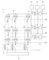
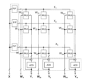
- the product-sum calculator comprises a resistive digital-to-analog conversion unit which includes a plurality of resistive digital-to-analog converters and converts the digital value of each element of an input vector into an analog voltage and outputs the analog voltage; a capacitive digital-to-analog conversion unit which includes a plurality of capacitive digital-to-analog converters and receives the analog voltage output from the resistive digital-to-analog conversion unit and sets a capacitance ratio between the input/output terminals and between the output terminal and ground corresponding to the digital value of each element of a matrix; a successive approximation type analog-to-digital conversion unit which includes a plurality of successive approximation type analog-to-digital converters and converts the voltage of a node commonly connected to each output terminal of the capacitive digital-to-analog conversion unit into a digital value and outputs the digital value; and a current consumption control unit which controls the current consumption of the resistive digital
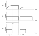
- the response is a step response of an RC circuit
- the set voltage is V s and the time constant is ⁇
- the error voltage V e can be expressed by the following formula 3.
- the conversion count control unit 15 controls the number of successive approximations in the successive approximation type analog-digital conversion unit 13.
- Fig. 3A is a circuit diagram showing the configuration of the successive approximation type ADC of the successive approximation type analog-digital conversion unit 13, and
- Fig. 3B is a conceptual diagram showing a method of reducing power consumption.
- the successive approximation type analog-digital conversion unit 13 is composed of a binary-weighted capacitance array C, a switch S for selecting a voltage to be applied to each capacitance from a ground potential or a reference voltage, a comparator for comparing voltages, and an SAR logic for controlling the successive approximation.
- the reference voltage control unit 16 controls the reference voltage of each successive approximation type ADC in the successive approximation type analog-digital conversion unit 13 so that the gain error of the ADC is minimized.
- Fig. 4 is a circuit diagram showing an example of the configuration of the reference voltage control unit 16.
- the reference voltage can also be controlled by connecting a capacitance ⁇ C (capacitance with a capacitance ratio ⁇ ) that samples an input signal as the reference voltage control unit 16 to a connection part of the input end of a binary-weighted capacitive digital-to-analog converter (DAC) and a comparator 21 that are provided in the successive approximation type analog-digital conversion unit 13 and generate a voltage difference between an input signal and a comparison voltage, as shown in Fig. 4.
- DAC binary-weighted capacitive digital-to-analog converter
- the switch S10 is closed, and the input signal V inp or the input signal V inn is selected by the switches S 11 , S 12 ... S n+10 of each capacitance of the capacitive DAC, thereby sampling the input signal.
- the switch S10 is opened, and the capacitance C/2 of the capacitive DAC is connected to the input signal V RP or the input signal V RN , and the remaining capacitances C/4 ... C/2 N-1 are connected to the ground GND.
- the potential difference (Va - Vb) at the input terminals of the comparator 21 when performing the most significant bit (MSB) comparison is expressed by the following formula 4.
- the adder 19 adds an arbitrary value to the output value from the successive approximation type analog-digital conversion section 13 to perform offset compensation, and the offset control section 20 controls the value added by the adder 19 .
Landscapes
- Engineering & Computer Science (AREA)
- Physics & Mathematics (AREA)
- Theoretical Computer Science (AREA)
- Mathematical Physics (AREA)
- General Physics & Mathematics (AREA)
- Computer Hardware Design (AREA)
- Software Systems (AREA)
- Health & Medical Sciences (AREA)
- Biomedical Technology (AREA)
- Neurology (AREA)
- General Engineering & Computer Science (AREA)
- General Health & Medical Sciences (AREA)
- Life Sciences & Earth Sciences (AREA)
- Biophysics (AREA)
- Computational Linguistics (AREA)
- Data Mining & Analysis (AREA)
- Evolutionary Computation (AREA)
- Artificial Intelligence (AREA)
- Computing Systems (AREA)
- Neurosurgery (AREA)
- Physiology (AREA)
- Molecular Biology (AREA)
- Human Computer Interaction (AREA)
- Power Engineering (AREA)
- Analogue/Digital Conversion (AREA)
Priority Applications (2)
| Application Number | Priority Date | Filing Date | Title |
|---|---|---|---|
| JP2024567758A JPWO2024143223A1 (https=) | 2022-12-26 | 2023-12-22 | |
| CN202380088909.4A CN120418802A (zh) | 2022-12-26 | 2023-12-22 | 积和运算器 |
Applications Claiming Priority (2)
| Application Number | Priority Date | Filing Date | Title |
|---|---|---|---|
| JP2022208738 | 2022-12-26 | ||
| JP2022-208738 | 2022-12-26 |
Publications (1)
| Publication Number | Publication Date |
|---|---|
| WO2024143223A1 true WO2024143223A1 (ja) | 2024-07-04 |
Family
ID=91717862
Family Applications (1)
| Application Number | Title | Priority Date | Filing Date |
|---|---|---|---|
| PCT/JP2023/046250 Ceased WO2024143223A1 (ja) | 2022-12-26 | 2023-12-22 | 積和演算器 |
Country Status (3)
| Country | Link |
|---|---|
| JP (1) | JPWO2024143223A1 (https=) |
| CN (1) | CN120418802A (https=) |
| WO (1) | WO2024143223A1 (https=) |
Citations (4)
| Publication number | Priority date | Publication date | Assignee | Title |
|---|---|---|---|---|
| JPH09259205A (ja) * | 1996-03-19 | 1997-10-03 | Yozan:Kk | 積和演算回路 |
| JP2010252247A (ja) * | 2009-04-20 | 2010-11-04 | Fujitsu Ltd | 電荷分配型デジタル・アナログ変換器及びそれを有する逐次比較型アナログ・デジタル変換器 |
| JP2020009112A (ja) * | 2018-07-06 | 2020-01-16 | 株式会社デンソー | ニューラルネットワーク回路 |
| WO2021171880A1 (ja) * | 2020-02-26 | 2021-09-02 | 株式会社テックイデア | 積和演算器 |
-
2023
- 2023-12-22 JP JP2024567758A patent/JPWO2024143223A1/ja active Pending
- 2023-12-22 WO PCT/JP2023/046250 patent/WO2024143223A1/ja not_active Ceased
- 2023-12-22 CN CN202380088909.4A patent/CN120418802A/zh active Pending
Patent Citations (4)
| Publication number | Priority date | Publication date | Assignee | Title |
|---|---|---|---|---|
| JPH09259205A (ja) * | 1996-03-19 | 1997-10-03 | Yozan:Kk | 積和演算回路 |
| JP2010252247A (ja) * | 2009-04-20 | 2010-11-04 | Fujitsu Ltd | 電荷分配型デジタル・アナログ変換器及びそれを有する逐次比較型アナログ・デジタル変換器 |
| JP2020009112A (ja) * | 2018-07-06 | 2020-01-16 | 株式会社デンソー | ニューラルネットワーク回路 |
| WO2021171880A1 (ja) * | 2020-02-26 | 2021-09-02 | 株式会社テックイデア | 積和演算器 |
Also Published As
| Publication number | Publication date |
|---|---|
| CN120418802A (zh) | 2025-08-01 |
| JPWO2024143223A1 (https=) | 2024-07-04 |
Similar Documents
| Publication | Publication Date | Title |
|---|---|---|
| US9654130B2 (en) | Analog-to-digital converters for successive approximation incorporating delta sigma analog-to-digital converters and hybrid digital-to-analog with charge-sharing and charge redistribution | |
| WO2020226898A1 (en) | Bit-ordered binary-weighted multiplier-accumulator | |
| KR101020672B1 (ko) | 비동기 전류모드 순환 비교를 이용한 아날로그-디지털 변환 | |
| Chang et al. | A 28-nm 10-b 2.2-GS/s 18.2-mW relative-prime time-interleaved sub-ranging SAR ADC with on-chip background skew calibration | |
| EP0730794B1 (en) | An efficient architecture for correcting component mismatches and circuit nonlinearities in a/d converters | |
| EP3537609A1 (en) | Method of applying a dither, and analog to digital converter operating in accordance with the method | |
| KR20170069140A (ko) | 플래시 지원 연속 근사 레지스터형 adc의 리던던시 장치 및 방법 | |
| KR20180105027A (ko) | 분할-커패시터 기반의 디지털-아날로그 변환기를 갖는 축차 근사형 아날로그-디지털 컨버터 | |
| KR20180122235A (ko) | 연속적인 근사 레지스터 아날로그 디지털 변환 장치 | |
| JPH11274927A (ja) | パイプライン接続a/d変換器のためのデジタル自己較正方式 | |
| CN102904573A (zh) | 模数转换器及模数转换方法 | |
| EP4035032A1 (en) | Successive bit-ordered binary-weighted multiplier-accumulator | |
| Stoops et al. | Digital background calibration of a split current-steering DAC | |
| CN109120263B (zh) | 一种基于数字调制校正的逐次逼近模数转换器 | |
| Baek et al. | A 600-MS/s, 65-dB SNDR, 75-MHz BW Time-Interleaved Noise-Shaping SAR ADC | |
| WO2024143223A1 (ja) | 積和演算器 | |
| US12261621B2 (en) | Successive approximation register (SAR) analog- to-digital converter (ADC) with input-dependent least significant bit (LSB) size | |
| Jiang et al. | A 16-bit 1MS/s weight borrowing SAR ADC with back propagation neural network calibration | |
| KR102921411B1 (ko) | 비동기 방식의 연속 근사 레지스터 아날로그 디지털 변환기 | |
| CN118138042A (zh) | 模拟数字转换器装置以及模拟前台校正方法 | |
| Pelgrom | Successive Approximation Conversion | |
| Zeloufi | A 12 bit 40 MSPS SAR ADC with a redundancy algorithm and digital calibration for the ATLAS LAr calorimeter readout | |
| US12489453B2 (en) | SAR ADC with bottom-plate sampling and mismatch error shaping | |
| US20250224928A1 (en) | Driving analog compute-in-memory cells using low power sparsity-aware digital-to-analog converters | |
| CN119893328B (zh) | 带有预判断逻辑的sar-ss型adc电路、模块 |
Legal Events
| Date | Code | Title | Description |
|---|---|---|---|
| 121 | Ep: the epo has been informed by wipo that ep was designated in this application |
Ref document number: 23912003 Country of ref document: EP Kind code of ref document: A1 |
|
| WWE | Wipo information: entry into national phase |
Ref document number: 2024567758 Country of ref document: JP |
|
| WWE | Wipo information: entry into national phase |
Ref document number: 202380088909.4 Country of ref document: CN |
|
| NENP | Non-entry into the national phase |
Ref country code: DE |
|
| WWP | Wipo information: published in national office |
Ref document number: 202380088909.4 Country of ref document: CN |
|
| 122 | Ep: pct application non-entry in european phase |
Ref document number: 23912003 Country of ref document: EP Kind code of ref document: A1 |