WO2024143218A1 - 電解コンデンサ - Google Patents
電解コンデンサ Download PDFInfo
- Publication number
- WO2024143218A1 WO2024143218A1 PCT/JP2023/046241 JP2023046241W WO2024143218A1 WO 2024143218 A1 WO2024143218 A1 WO 2024143218A1 JP 2023046241 W JP2023046241 W JP 2023046241W WO 2024143218 A1 WO2024143218 A1 WO 2024143218A1
- Authority
- WO
- WIPO (PCT)
- Prior art keywords
- layer
- metal foil
- electrolytic capacitor
- cathode
- anode
- Prior art date
- Legal status (The legal status is an assumption and is not a legal conclusion. Google has not performed a legal analysis and makes no representation as to the accuracy of the status listed.)
- Ceased
Links
Images




Classifications
-
- H—ELECTRICITY
- H01—ELECTRIC ELEMENTS
- H01G—CAPACITORS; CAPACITORS, RECTIFIERS, DETECTORS, SWITCHING DEVICES, LIGHT-SENSITIVE OR TEMPERATURE-SENSITIVE DEVICES OF THE ELECTROLYTIC TYPE
- H01G9/00—Electrolytic capacitors, rectifiers, detectors, switching devices, light-sensitive or temperature-sensitive devices; Processes of their manufacture
- H01G9/15—Solid electrolytic capacitors
-
- H—ELECTRICITY
- H01—ELECTRIC ELEMENTS
- H01G—CAPACITORS; CAPACITORS, RECTIFIERS, DETECTORS, SWITCHING DEVICES, LIGHT-SENSITIVE OR TEMPERATURE-SENSITIVE DEVICES OF THE ELECTROLYTIC TYPE
- H01G9/00—Electrolytic capacitors, rectifiers, detectors, switching devices, light-sensitive or temperature-sensitive devices; Processes of their manufacture
- H01G9/004—Details
- H01G9/008—Terminals
- H01G9/012—Terminals specially adapted for solid capacitors
-
- H—ELECTRICITY
- H01—ELECTRIC ELEMENTS
- H01G—CAPACITORS; CAPACITORS, RECTIFIERS, DETECTORS, SWITCHING DEVICES, LIGHT-SENSITIVE OR TEMPERATURE-SENSITIVE DEVICES OF THE ELECTROLYTIC TYPE
- H01G9/00—Electrolytic capacitors, rectifiers, detectors, switching devices, light-sensitive or temperature-sensitive devices; Processes of their manufacture
- H01G9/004—Details
- H01G9/04—Electrodes or formation of dielectric layers thereon
- H01G9/042—Electrodes or formation of dielectric layers thereon characterised by the material
-
- H—ELECTRICITY
- H01—ELECTRIC ELEMENTS
- H01G—CAPACITORS; CAPACITORS, RECTIFIERS, DETECTORS, SWITCHING DEVICES, LIGHT-SENSITIVE OR TEMPERATURE-SENSITIVE DEVICES OF THE ELECTROLYTIC TYPE
- H01G9/00—Electrolytic capacitors, rectifiers, detectors, switching devices, light-sensitive or temperature-sensitive devices; Processes of their manufacture
- H01G9/004—Details
- H01G9/04—Electrodes or formation of dielectric layers thereon
- H01G9/042—Electrodes or formation of dielectric layers thereon characterised by the material
- H01G9/0425—Electrodes or formation of dielectric layers thereon characterised by the material specially adapted for cathode
-
- H—ELECTRICITY
- H01—ELECTRIC ELEMENTS
- H01G—CAPACITORS; CAPACITORS, RECTIFIERS, DETECTORS, SWITCHING DEVICES, LIGHT-SENSITIVE OR TEMPERATURE-SENSITIVE DEVICES OF THE ELECTROLYTIC TYPE
- H01G9/00—Electrolytic capacitors, rectifiers, detectors, switching devices, light-sensitive or temperature-sensitive devices; Processes of their manufacture
- H01G9/004—Details
- H01G9/04—Electrodes or formation of dielectric layers thereon
- H01G9/042—Electrodes or formation of dielectric layers thereon characterised by the material
- H01G9/045—Electrodes or formation of dielectric layers thereon characterised by the material based on aluminium
-
- H—ELECTRICITY
- H01—ELECTRIC ELEMENTS
- H01G—CAPACITORS; CAPACITORS, RECTIFIERS, DETECTORS, SWITCHING DEVICES, LIGHT-SENSITIVE OR TEMPERATURE-SENSITIVE DEVICES OF THE ELECTROLYTIC TYPE
- H01G9/00—Electrolytic capacitors, rectifiers, detectors, switching devices, light-sensitive or temperature-sensitive devices; Processes of their manufacture
- H01G9/004—Details
- H01G9/04—Electrodes or formation of dielectric layers thereon
- H01G9/048—Electrodes or formation of dielectric layers thereon characterised by their structure
-
- H—ELECTRICITY
- H01—ELECTRIC ELEMENTS
- H01G—CAPACITORS; CAPACITORS, RECTIFIERS, DETECTORS, SWITCHING DEVICES, LIGHT-SENSITIVE OR TEMPERATURE-SENSITIVE DEVICES OF THE ELECTROLYTIC TYPE
- H01G9/00—Electrolytic capacitors, rectifiers, detectors, switching devices, light-sensitive or temperature-sensitive devices; Processes of their manufacture
- H01G9/004—Details
- H01G9/04—Electrodes or formation of dielectric layers thereon
- H01G9/048—Electrodes or formation of dielectric layers thereon characterised by their structure
- H01G9/055—Etched foil electrodes
-
- H—ELECTRICITY
- H01—ELECTRIC ELEMENTS
- H01G—CAPACITORS; CAPACITORS, RECTIFIERS, DETECTORS, SWITCHING DEVICES, LIGHT-SENSITIVE OR TEMPERATURE-SENSITIVE DEVICES OF THE ELECTROLYTIC TYPE
- H01G9/00—Electrolytic capacitors, rectifiers, detectors, switching devices, light-sensitive or temperature-sensitive devices; Processes of their manufacture
- H01G9/004—Details
- H01G9/08—Housing; Encapsulation
-
- H—ELECTRICITY
- H01—ELECTRIC ELEMENTS
- H01G—CAPACITORS; CAPACITORS, RECTIFIERS, DETECTORS, SWITCHING DEVICES, LIGHT-SENSITIVE OR TEMPERATURE-SENSITIVE DEVICES OF THE ELECTROLYTIC TYPE
- H01G9/00—Electrolytic capacitors, rectifiers, detectors, switching devices, light-sensitive or temperature-sensitive devices; Processes of their manufacture
- H01G9/004—Details
- H01G9/08—Housing; Encapsulation
- H01G9/10—Sealing, e.g. of lead-in wires
-
- H—ELECTRICITY
- H01—ELECTRIC ELEMENTS
- H01G—CAPACITORS; CAPACITORS, RECTIFIERS, DETECTORS, SWITCHING DEVICES, LIGHT-SENSITIVE OR TEMPERATURE-SENSITIVE DEVICES OF THE ELECTROLYTIC TYPE
- H01G9/00—Electrolytic capacitors, rectifiers, detectors, switching devices, light-sensitive or temperature-sensitive devices; Processes of their manufacture
- H01G9/004—Details
- H01G9/14—Structural combinations or circuits for modifying, or compensating for, electric characteristics of electrolytic capacitors
Definitions
- the adhesive strength between the metal foil and the capacitor element (cathode) via the conductive adhesive layer is low. This means that peeling between the metal foil and the capacitor element (hereinafter also referred to as “lamination peeling”) is likely to occur, increasing the contact resistance. In addition, misalignment between the capacitor element and the metal foil (hereinafter also referred to as “lamination misalignment”) is likely to occur when sealing the capacitor element. As a result, the reliability of the electrolytic capacitor is reduced.
- One aspect of the present disclosure provides a capacitor including a capacitor element having an anode portion and a cathode portion, an exterior body sealing the capacitor element, a metal foil electrically connected to the cathode portion, a first external electrode electrically connected to the metal foil, and a conductive adhesive layer;
- the present invention relates to an electrolytic capacitor, wherein the metal foil has a through hole penetrating in the thickness direction, the conductive adhesive layer includes a first layer interposed between the cathode portion and a main surface of the metal foil and a second layer filled in the through hole, the first layer and the second layer being integrated, and the metal foil has a first end face exposed from the outer casing, and the first end face is electrically connected to the first external electrode.
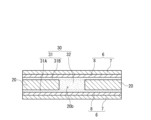
- FIG. 1 is a cross-sectional view illustrating a schematic example of an electrolytic capacitor according to an embodiment of the present disclosure.
- 2 is an enlarged schematic cross-sectional view of a main portion near a metal foil disposed between adjacent capacitor elements of the element laminate of the electrolytic capacitor shown in FIG. 1 .
- 2 is an enlarged schematic cross-sectional view of a main portion in the vicinity of a metal foil disposed at one end of the element laminate of the electrolytic capacitor shown in FIG. 1 .
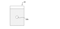
- FIG. 2 is a top view showing a schematic diagram of an example of a metal foil having one through-hole having a circular cross section.
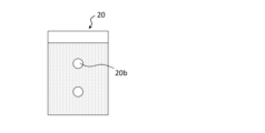
- FIG. 2 is a top view showing a schematic diagram of an example of a metal foil having two through holes each having a circular cross section.
- FIG. 2 is a top view showing a schematic diagram of an example of a metal foil having five through holes each having a circular cross section.
- FIG. 2 is a top view showing a schematic diagram of an example of a metal foil having three through holes each having a linear cross section.
- FIG. 2 is a top view showing a schematic diagram of an example of a metal foil having five through holes each having a linear cross section.
- FIG. 2 is a top view showing a schematic diagram of an example of a metal foil having seven through holes each having a linear cross section.
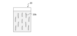
- FIG. 2 is a top view showing a schematic diagram of an example of a metal foil having nine through holes each having a linear cross section.
- FIG. 2 is a top view showing a schematic diagram of an example of a metal foil having eleven through-holes each having a linear cross section.
- the embodiments of the present disclosure are described using examples, but the present disclosure is not limited to the examples described below.
- specific numerical values and materials may be exemplified, but other numerical values and materials may be applied as long as the effects of the present disclosure are obtained.
- the expression "numerical value A to numerical value B" includes numerical value A and numerical value B and can be read as "numerical value A or more and numerical value B or less.”
- any of the exemplified lower limits and any of the exemplified upper limits can be arbitrarily combined as long as the lower limit is not equal to or greater than the upper limit.
- one of the materials may be selected and used alone, or two or more of the materials may be used in combination.
- the present disclosure encompasses a combination of the features described in two or more claims arbitrarily selected from the multiple claims described in the appended claims.
- the features described in two or more claims arbitrarily selected from the multiple claims described in the appended claims may be combined, provided that no technical contradiction arises.
- the conductive adhesive layer may be formed, for example, by applying a conductive adhesive to one main surface of the metal foil (the area to be attached to the cathode portion), placing a capacitor element (cathode portion) on top of the conductive adhesive, and then filling the through-hole on the other main surface of the metal foil with the conductive adhesive through the opening of the through-hole. If a capacitor element (cathode portion) is then separately placed on the other main surface of the metal foil, the conductive adhesive may be applied on the conductive adhesive filled in the other main surface of the metal foil and the through-hole, and the capacitor element (cathode portion) may be placed on top of the conductive adhesive.
- the separation layer may contain, for example, a resin, and may be one of the examples of the exterior body described below.
- the dielectric layer formed in the porous portion of the first part may be compressed and densified to provide insulation.
- Laminated samples a1 to a4 had a larger breaking load and higher adhesive strength than laminated sample b1.
- laminated samples a1 to a3 which had a through-hole ratio of 15% or less, had excellent adhesive strength.
Landscapes
- Engineering & Computer Science (AREA)
- Power Engineering (AREA)
- Microelectronics & Electronic Packaging (AREA)
- Chemical & Material Sciences (AREA)
- Materials Engineering (AREA)
- Fixed Capacitors And Capacitor Manufacturing Machines (AREA)
Priority Applications (3)
| Application Number | Priority Date | Filing Date | Title |
|---|---|---|---|
| CN202380088131.7A CN120418909A (zh) | 2022-12-27 | 2023-12-22 | 电解电容器 |
| JP2024567754A JPWO2024143218A1 (https=) | 2022-12-27 | 2023-12-22 | |
| US19/235,189 US20250308809A1 (en) | 2022-12-27 | 2025-06-11 | Electrolytic capacitor |
Applications Claiming Priority (2)
| Application Number | Priority Date | Filing Date | Title |
|---|---|---|---|
| JP2022210806 | 2022-12-27 | ||
| JP2022-210806 | 2022-12-27 |
Related Child Applications (1)
| Application Number | Title | Priority Date | Filing Date |
|---|---|---|---|
| US19/235,189 Continuation US20250308809A1 (en) | 2022-12-27 | 2025-06-11 | Electrolytic capacitor |
Publications (1)
| Publication Number | Publication Date |
|---|---|
| WO2024143218A1 true WO2024143218A1 (ja) | 2024-07-04 |
Family
ID=91717946
Family Applications (1)
| Application Number | Title | Priority Date | Filing Date |
|---|---|---|---|
| PCT/JP2023/046241 Ceased WO2024143218A1 (ja) | 2022-12-27 | 2023-12-22 | 電解コンデンサ |
Country Status (4)
| Country | Link |
|---|---|
| US (1) | US20250308809A1 (https=) |
| JP (1) | JPWO2024143218A1 (https=) |
| CN (1) | CN120418909A (https=) |
| WO (1) | WO2024143218A1 (https=) |
Citations (3)
| Publication number | Priority date | Publication date | Assignee | Title |
|---|---|---|---|---|
| JPH0582401A (ja) * | 1991-09-20 | 1993-04-02 | Nippon Chemicon Corp | 固体電解コンデンサ |
| WO2017090241A1 (ja) * | 2015-11-27 | 2017-06-01 | パナソニックIpマネジメント株式会社 | 電解コンデンサおよびその製造方法 |
| WO2021125045A1 (ja) * | 2019-12-18 | 2021-06-24 | 株式会社村田製作所 | 固体電解コンデンサ |
-
2023
- 2023-12-22 WO PCT/JP2023/046241 patent/WO2024143218A1/ja not_active Ceased
- 2023-12-22 CN CN202380088131.7A patent/CN120418909A/zh active Pending
- 2023-12-22 JP JP2024567754A patent/JPWO2024143218A1/ja active Pending
-
2025
- 2025-06-11 US US19/235,189 patent/US20250308809A1/en active Pending
Patent Citations (3)
| Publication number | Priority date | Publication date | Assignee | Title |
|---|---|---|---|---|
| JPH0582401A (ja) * | 1991-09-20 | 1993-04-02 | Nippon Chemicon Corp | 固体電解コンデンサ |
| WO2017090241A1 (ja) * | 2015-11-27 | 2017-06-01 | パナソニックIpマネジメント株式会社 | 電解コンデンサおよびその製造方法 |
| WO2021125045A1 (ja) * | 2019-12-18 | 2021-06-24 | 株式会社村田製作所 | 固体電解コンデンサ |
Also Published As
| Publication number | Publication date |
|---|---|
| CN120418909A (zh) | 2025-08-01 |
| JPWO2024143218A1 (https=) | 2024-07-04 |
| US20250308809A1 (en) | 2025-10-02 |
Similar Documents
| Publication | Publication Date | Title |
|---|---|---|
| US12476053B2 (en) | Electrolytic capacitor and manufacturing method thereof | |
| CN109791844B (zh) | 固体电解电容器 | |
| KR100907600B1 (ko) | 고체 전해 콘덴서 | |
| JP7706069B2 (ja) | 電解コンデンサおよびその製造方法 | |
| JP7796337B2 (ja) | 電解コンデンサ | |
| JP7724459B2 (ja) | 電解コンデンサ | |
| WO2022163644A1 (ja) | 電解コンデンサ | |
| US7957120B2 (en) | Capacitor chip and method for manufacturing same | |
| WO2024143218A1 (ja) | 電解コンデンサ | |
| WO2023120383A1 (ja) | 電解コンデンサおよびその製造方法 | |
| JP2023150741A (ja) | 固体電解コンデンサ | |
| WO2025047767A1 (ja) | 電解コンデンサ | |
| WO2024143173A1 (ja) | 固体電解コンデンサ | |
| CN114981905A (zh) | 电解电容器 | |
| US20260004970A1 (en) | Solid electrolytic capacitor and method for manufacturing same | |
| JP7526925B2 (ja) | 固体電解コンデンサ素子および固体電解コンデンサ | |
| WO2025263573A1 (ja) | 固体電解コンデンサおよび固体電解コンデンサの製造方法 | |
| JP2018117087A (ja) | 固体電解コンデンサおよびその製造方法 |
Legal Events
| Date | Code | Title | Description |
|---|---|---|---|
| 121 | Ep: the epo has been informed by wipo that ep was designated in this application |
Ref document number: 23911998 Country of ref document: EP Kind code of ref document: A1 |
|
| WWE | Wipo information: entry into national phase |
Ref document number: 202380088131.7 Country of ref document: CN |
|
| WWE | Wipo information: entry into national phase |
Ref document number: 2024567754 Country of ref document: JP |
|
| NENP | Non-entry into the national phase |
Ref country code: DE |
|
| WWP | Wipo information: published in national office |
Ref document number: 202380088131.7 Country of ref document: CN |
|
| 122 | Ep: pct application non-entry in european phase |
Ref document number: 23911998 Country of ref document: EP Kind code of ref document: A1 |