WO2024143218A1 - Electrolytic capacitor - Google Patents
Electrolytic capacitor Download PDFInfo
- Publication number
- WO2024143218A1 WO2024143218A1 PCT/JP2023/046241 JP2023046241W WO2024143218A1 WO 2024143218 A1 WO2024143218 A1 WO 2024143218A1 JP 2023046241 W JP2023046241 W JP 2023046241W WO 2024143218 A1 WO2024143218 A1 WO 2024143218A1
- Authority
- WO
- WIPO (PCT)
- Prior art keywords
- layer
- metal foil
- electrolytic capacitor
- cathode
- anode
- Prior art date
Links
- 239000003990 capacitor Substances 0.000 title claims abstract description 205
- 239000010410 layer Substances 0.000 claims abstract description 342
- 229910052751 metal Inorganic materials 0.000 claims abstract description 201
- 239000002184 metal Substances 0.000 claims abstract description 201
- 239000011888 foil Substances 0.000 claims abstract description 182
- 239000012790 adhesive layer Substances 0.000 claims abstract description 43
- 239000000758 substrate Substances 0.000 claims description 61
- 229920005989 resin Polymers 0.000 claims description 46
- 239000011347 resin Substances 0.000 claims description 46
- OKTJSMMVPCPJKN-UHFFFAOYSA-N Carbon Chemical compound [C] OKTJSMMVPCPJKN-UHFFFAOYSA-N 0.000 claims description 34
- 239000007784 solid electrolyte Substances 0.000 claims description 32
- 229910052799 carbon Inorganic materials 0.000 claims description 31
- PXHVJJICTQNCMI-UHFFFAOYSA-N Nickel Chemical compound [Ni] PXHVJJICTQNCMI-UHFFFAOYSA-N 0.000 claims description 28
- 239000002245 particle Substances 0.000 claims description 22
- 239000011247 coating layer Substances 0.000 claims description 14
- 238000000605 extraction Methods 0.000 claims description 11
- 229910052782 aluminium Inorganic materials 0.000 claims description 9
- XAGFODPZIPBFFR-UHFFFAOYSA-N aluminium Chemical compound [Al] XAGFODPZIPBFFR-UHFFFAOYSA-N 0.000 claims description 9
- 239000002923 metal particle Substances 0.000 claims description 9
- RTAQQCXQSZGOHL-UHFFFAOYSA-N Titanium Chemical compound [Ti] RTAQQCXQSZGOHL-UHFFFAOYSA-N 0.000 claims description 8
- 239000010936 titanium Substances 0.000 claims description 8
- 229910052719 titanium Inorganic materials 0.000 claims description 8
- 239000010949 copper Substances 0.000 claims description 7
- RYGMFSIKBFXOCR-UHFFFAOYSA-N Copper Chemical compound [Cu] RYGMFSIKBFXOCR-UHFFFAOYSA-N 0.000 claims description 6
- 229910052802 copper Inorganic materials 0.000 claims description 6
- 229910052759 nickel Inorganic materials 0.000 claims description 5
- 230000000149 penetrating effect Effects 0.000 claims description 5
- 229910000838 Al alloy Inorganic materials 0.000 claims description 3
- 229910000881 Cu alloy Inorganic materials 0.000 claims description 3
- GWEVSGVZZGPLCZ-UHFFFAOYSA-N Titan oxide Chemical compound O=[Ti]=O GWEVSGVZZGPLCZ-UHFFFAOYSA-N 0.000 claims description 3
- NRTOMJZYCJJWKI-UHFFFAOYSA-N Titanium nitride Chemical compound [Ti]#N NRTOMJZYCJJWKI-UHFFFAOYSA-N 0.000 claims description 3
- OGIDPMRJRNCKJF-UHFFFAOYSA-N titanium oxide Inorganic materials [Ti]=O OGIDPMRJRNCKJF-UHFFFAOYSA-N 0.000 claims description 3
- MTPVUVINMAGMJL-UHFFFAOYSA-N trimethyl(1,1,2,2,2-pentafluoroethyl)silane Chemical compound C[Si](C)(C)C(F)(F)C(F)(F)F MTPVUVINMAGMJL-UHFFFAOYSA-N 0.000 claims description 3
- 238000000034 method Methods 0.000 description 43
- 230000001070 adhesive effect Effects 0.000 description 30
- 239000000853 adhesive Substances 0.000 description 29
- 238000007747 plating Methods 0.000 description 24
- 239000000463 material Substances 0.000 description 23
- 238000000926 separation method Methods 0.000 description 16
- 239000011248 coating agent Substances 0.000 description 15
- 238000000576 coating method Methods 0.000 description 12
- 239000003822 epoxy resin Substances 0.000 description 11
- 229920000647 polyepoxide Polymers 0.000 description 11
- 229910052709 silver Inorganic materials 0.000 description 10
- 229920005992 thermoplastic resin Polymers 0.000 description 10
- BQCADISMDOOEFD-UHFFFAOYSA-N Silver Chemical compound [Ag] BQCADISMDOOEFD-UHFFFAOYSA-N 0.000 description 9
- 239000000945 filler Substances 0.000 description 9
- 239000004332 silver Substances 0.000 description 9
- 239000000126 substance Substances 0.000 description 9
- 230000008961 swelling Effects 0.000 description 9
- 238000010586 diagram Methods 0.000 description 8
- 238000011156 evaluation Methods 0.000 description 8
- 239000007787 solid Substances 0.000 description 8
- 238000006243 chemical reaction Methods 0.000 description 7
- -1 fluororesin Polymers 0.000 description 7
- 239000007788 liquid Substances 0.000 description 7
- 229920000547 conjugated polymer Polymers 0.000 description 6
- 230000007423 decrease Effects 0.000 description 6
- 239000007789 gas Substances 0.000 description 6
- 230000008569 process Effects 0.000 description 6
- 239000011342 resin composition Substances 0.000 description 6
- 230000015572 biosynthetic process Effects 0.000 description 5
- 239000002019 doping agent Substances 0.000 description 5
- 230000000694 effects Effects 0.000 description 5
- 238000005530 etching Methods 0.000 description 5
- 238000011049 filling Methods 0.000 description 5
- 238000003475 lamination Methods 0.000 description 5
- 238000012545 processing Methods 0.000 description 5
- 238000007789 sealing Methods 0.000 description 5
- 239000000243 solution Substances 0.000 description 5
- 239000002904 solvent Substances 0.000 description 5
- 239000002344 surface layer Substances 0.000 description 5
- 239000003795 chemical substances by application Substances 0.000 description 4
- 150000001875 compounds Chemical class 0.000 description 4
- 239000011521 glass Substances 0.000 description 4
- 239000000203 mixture Substances 0.000 description 4
- 239000003505 polymerization initiator Substances 0.000 description 4
- 229910052718 tin Inorganic materials 0.000 description 4
- XLYOFNOQVPJJNP-UHFFFAOYSA-N water Substances O XLYOFNOQVPJJNP-UHFFFAOYSA-N 0.000 description 4
- ATJFFYVFTNAWJD-UHFFFAOYSA-N Tin Chemical compound [Sn] ATJFFYVFTNAWJD-UHFFFAOYSA-N 0.000 description 3
- 229910045601 alloy Inorganic materials 0.000 description 3
- 239000000956 alloy Substances 0.000 description 3
- 239000003054 catalyst Substances 0.000 description 3
- 238000005229 chemical vapour deposition Methods 0.000 description 3
- 229920001577 copolymer Polymers 0.000 description 3
- 239000006185 dispersion Substances 0.000 description 3
- 239000010931 gold Substances 0.000 description 3
- 238000010438 heat treatment Methods 0.000 description 3
- 230000000873 masking effect Effects 0.000 description 3
- 229920001721 polyimide Polymers 0.000 description 3
- 239000002243 precursor Substances 0.000 description 3
- LBLYYCQCTBFVLH-UHFFFAOYSA-N 2-Methylbenzenesulfonic acid Chemical compound CC1=CC=CC=C1S(O)(=O)=O LBLYYCQCTBFVLH-UHFFFAOYSA-N 0.000 description 2
- 239000004593 Epoxy Substances 0.000 description 2
- 229920001609 Poly(3,4-ethylenedioxythiophene) Polymers 0.000 description 2
- 239000004642 Polyimide Substances 0.000 description 2
- 239000004734 Polyphenylene sulfide Substances 0.000 description 2
- VYPSYNLAJGMNEJ-UHFFFAOYSA-N Silicium dioxide Chemical compound O=[Si]=O VYPSYNLAJGMNEJ-UHFFFAOYSA-N 0.000 description 2
- 230000009471 action Effects 0.000 description 2
- 230000004075 alteration Effects 0.000 description 2
- 239000011230 binding agent Substances 0.000 description 2
- IISBACLAFKSPIT-UHFFFAOYSA-N bisphenol A Chemical compound C=1C=C(O)C=CC=1C(C)(C)C1=CC=C(O)C=C1 IISBACLAFKSPIT-UHFFFAOYSA-N 0.000 description 2
- PXKLMJQFEQBVLD-UHFFFAOYSA-N bisphenol F Chemical compound C1=CC(O)=CC=C1CC1=CC=C(O)C=C1 PXKLMJQFEQBVLD-UHFFFAOYSA-N 0.000 description 2
- 230000015556 catabolic process Effects 0.000 description 2
- 230000008859 change Effects 0.000 description 2
- 230000000052 comparative effect Effects 0.000 description 2
- 229920001940 conductive polymer Polymers 0.000 description 2
- 239000004020 conductor Substances 0.000 description 2
- 238000006731 degradation reaction Methods 0.000 description 2
- 230000032798 delamination Effects 0.000 description 2
- 238000000151 deposition Methods 0.000 description 2
- 230000008021 deposition Effects 0.000 description 2
- 238000001035 drying Methods 0.000 description 2
- 238000000866 electrolytic etching Methods 0.000 description 2
- 229920006332 epoxy adhesive Polymers 0.000 description 2
- PCHJSUWPFVWCPO-UHFFFAOYSA-N gold Chemical compound [Au] PCHJSUWPFVWCPO-UHFFFAOYSA-N 0.000 description 2
- 229910052737 gold Inorganic materials 0.000 description 2
- 229910002804 graphite Inorganic materials 0.000 description 2
- 239000010439 graphite Substances 0.000 description 2
- 239000011810 insulating material Substances 0.000 description 2
- 238000005259 measurement Methods 0.000 description 2
- 150000002736 metal compounds Chemical class 0.000 description 2
- 150000002739 metals Chemical class 0.000 description 2
- 238000012986 modification Methods 0.000 description 2
- 230000004048 modification Effects 0.000 description 2
- 238000000465 moulding Methods 0.000 description 2
- PSZYNBSKGUBXEH-UHFFFAOYSA-N naphthalene-1-sulfonic acid Chemical compound C1=CC=C2C(S(=O)(=O)O)=CC=CC2=C1 PSZYNBSKGUBXEH-UHFFFAOYSA-N 0.000 description 2
- 239000003960 organic solvent Substances 0.000 description 2
- TWNQGVIAIRXVLR-UHFFFAOYSA-N oxo(oxoalumanyloxy)alumane Chemical compound O=[Al]O[Al]=O TWNQGVIAIRXVLR-UHFFFAOYSA-N 0.000 description 2
- 229920000172 poly(styrenesulfonic acid) Polymers 0.000 description 2
- 229920001707 polybutylene terephthalate Polymers 0.000 description 2
- 238000006116 polymerization reaction Methods 0.000 description 2
- 229920000069 polyphenylene sulfide Polymers 0.000 description 2
- 229940005642 polystyrene sulfonic acid Drugs 0.000 description 2
- 229920000123 polythiophene Polymers 0.000 description 2
- 238000004080 punching Methods 0.000 description 2
- 238000007788 roughening Methods 0.000 description 2
- 229910000679 solder Inorganic materials 0.000 description 2
- 239000007921 spray Substances 0.000 description 2
- 238000004544 sputter deposition Methods 0.000 description 2
- 230000003746 surface roughness Effects 0.000 description 2
- 229920001187 thermosetting polymer Polymers 0.000 description 2
- 238000001771 vacuum deposition Methods 0.000 description 2
- 229920000178 Acrylic resin Polymers 0.000 description 1
- 239000004925 Acrylic resin Substances 0.000 description 1
- 239000004641 Diallyl-phthalate Substances 0.000 description 1
- YCKRFDGAMUMZLT-UHFFFAOYSA-N Fluorine atom Chemical compound [F] YCKRFDGAMUMZLT-UHFFFAOYSA-N 0.000 description 1
- 239000002033 PVDF binder Substances 0.000 description 1
- 239000004813 Perfluoroalkoxy alkane Substances 0.000 description 1
- ISWSIDIOOBJBQZ-UHFFFAOYSA-N Phenol Chemical compound OC1=CC=CC=C1 ISWSIDIOOBJBQZ-UHFFFAOYSA-N 0.000 description 1
- 239000004962 Polyamide-imide Substances 0.000 description 1
- 229920001807 Urea-formaldehyde Polymers 0.000 description 1
- 238000010521 absorption reaction Methods 0.000 description 1
- 239000000654 additive Substances 0.000 description 1
- PNEYBMLMFCGWSK-UHFFFAOYSA-N aluminium oxide Inorganic materials [O-2].[O-2].[O-2].[Al+3].[Al+3] PNEYBMLMFCGWSK-UHFFFAOYSA-N 0.000 description 1
- 238000007743 anodising Methods 0.000 description 1
- 229910021383 artificial graphite Inorganic materials 0.000 description 1
- QUDWYFHPNIMBFC-UHFFFAOYSA-N bis(prop-2-enyl) benzene-1,2-dicarboxylate Chemical compound C=CCOC(=O)C1=CC=CC=C1C(=O)OCC=C QUDWYFHPNIMBFC-UHFFFAOYSA-N 0.000 description 1
- 239000003575 carbonaceous material Substances 0.000 description 1
- 239000004927 clay Substances 0.000 description 1
- 229910052570 clay Inorganic materials 0.000 description 1
- 238000004140 cleaning Methods 0.000 description 1
- 239000003431 cross linking reagent Substances 0.000 description 1
- 239000002612 dispersion medium Substances 0.000 description 1
- 238000007772 electroless plating Methods 0.000 description 1
- 238000000313 electron-beam-induced deposition Methods 0.000 description 1
- 238000009713 electroplating Methods 0.000 description 1
- 239000000835 fiber Substances 0.000 description 1
- 229910052731 fluorine Inorganic materials 0.000 description 1
- 239000011737 fluorine Substances 0.000 description 1
- LNEPOXFFQSENCJ-UHFFFAOYSA-N haloperidol Chemical compound C1CC(O)(C=2C=CC(Cl)=CC=2)CCN1CCCC(=O)C1=CC=C(F)C=C1 LNEPOXFFQSENCJ-UHFFFAOYSA-N 0.000 description 1
- 229910052739 hydrogen Inorganic materials 0.000 description 1
- 239000001257 hydrogen Substances 0.000 description 1
- 150000003949 imides Chemical class 0.000 description 1
- 230000001771 impaired effect Effects 0.000 description 1
- 238000005470 impregnation Methods 0.000 description 1
- 238000001746 injection moulding Methods 0.000 description 1
- 229910010272 inorganic material Inorganic materials 0.000 description 1
- 239000011147 inorganic material Substances 0.000 description 1
- 229910052500 inorganic mineral Inorganic materials 0.000 description 1
- 238000009413 insulation Methods 0.000 description 1
- 239000012212 insulator Substances 0.000 description 1
- 229910000765 intermetallic Inorganic materials 0.000 description 1
- 150000002697 manganese compounds Chemical class 0.000 description 1
- 238000004519 manufacturing process Methods 0.000 description 1
- 150000001247 metal acetylides Chemical class 0.000 description 1
- 229910044991 metal oxide Inorganic materials 0.000 description 1
- 150000004706 metal oxides Chemical class 0.000 description 1
- 239000010445 mica Substances 0.000 description 1
- 229910052618 mica group Inorganic materials 0.000 description 1
- 239000011707 mineral Substances 0.000 description 1
- 239000000178 monomer Substances 0.000 description 1
- 229910021382 natural graphite Inorganic materials 0.000 description 1
- 229910052758 niobium Inorganic materials 0.000 description 1
- 239000010955 niobium Substances 0.000 description 1
- GUCVJGMIXFAOAE-UHFFFAOYSA-N niobium atom Chemical compound [Nb] GUCVJGMIXFAOAE-UHFFFAOYSA-N 0.000 description 1
- 150000004767 nitrides Chemical class 0.000 description 1
- 229910052755 nonmetal Inorganic materials 0.000 description 1
- 229910052763 palladium Inorganic materials 0.000 description 1
- 229920011301 perfluoro alkoxyl alkane Polymers 0.000 description 1
- 239000005011 phenolic resin Substances 0.000 description 1
- 239000013034 phenoxy resin Substances 0.000 description 1
- 229920006287 phenoxy resin Polymers 0.000 description 1
- 230000000704 physical effect Effects 0.000 description 1
- 229920006122 polyamide resin Polymers 0.000 description 1
- 229920002312 polyamide-imide Polymers 0.000 description 1
- 229920000767 polyaniline Polymers 0.000 description 1
- 229920001225 polyester resin Polymers 0.000 description 1
- 239000004645 polyester resin Substances 0.000 description 1
- 239000009719 polyimide resin Substances 0.000 description 1
- 230000000379 polymerizing effect Effects 0.000 description 1
- 229920005672 polyolefin resin Polymers 0.000 description 1
- 229920000128 polypyrrole Polymers 0.000 description 1
- 229920001343 polytetrafluoroethylene Polymers 0.000 description 1
- 239000004810 polytetrafluoroethylene Substances 0.000 description 1
- 229920002635 polyurethane Polymers 0.000 description 1
- 239000004814 polyurethane Substances 0.000 description 1
- 229920005749 polyurethane resin Polymers 0.000 description 1
- 229920002981 polyvinylidene fluoride Polymers 0.000 description 1
- 239000011148 porous material Substances 0.000 description 1
- 238000002360 preparation method Methods 0.000 description 1
- 239000000377 silicon dioxide Substances 0.000 description 1
- 239000002356 single layer Substances 0.000 description 1
- 239000000454 talc Substances 0.000 description 1
- 229910052623 talc Inorganic materials 0.000 description 1
- 229910052715 tantalum Inorganic materials 0.000 description 1
- GUVRBAGPIYLISA-UHFFFAOYSA-N tantalum atom Chemical compound [Ta] GUVRBAGPIYLISA-UHFFFAOYSA-N 0.000 description 1
- JBQYATWDVHIOAR-UHFFFAOYSA-N tellanylidenegermanium Chemical compound [Te]=[Ge] JBQYATWDVHIOAR-UHFFFAOYSA-N 0.000 description 1
- 238000009864 tensile test Methods 0.000 description 1
- 150000003609 titanium compounds Chemical class 0.000 description 1
- 229920006305 unsaturated polyester Polymers 0.000 description 1
- 125000000391 vinyl group Chemical group [H]C([*])=C([H])[H] 0.000 description 1
- 229920002554 vinyl polymer Polymers 0.000 description 1
- NWONKYPBYAMBJT-UHFFFAOYSA-L zinc sulfate Chemical compound [Zn+2].[O-]S([O-])(=O)=O NWONKYPBYAMBJT-UHFFFAOYSA-L 0.000 description 1
Images


Classifications
-
- H—ELECTRICITY
- H01—ELECTRIC ELEMENTS
- H01G—CAPACITORS; CAPACITORS, RECTIFIERS, DETECTORS, SWITCHING DEVICES, LIGHT-SENSITIVE OR TEMPERATURE-SENSITIVE DEVICES OF THE ELECTROLYTIC TYPE
- H01G9/00—Electrolytic capacitors, rectifiers, detectors, switching devices, light-sensitive or temperature-sensitive devices; Processes of their manufacture
- H01G9/004—Details
- H01G9/04—Electrodes or formation of dielectric layers thereon
- H01G9/042—Electrodes or formation of dielectric layers thereon characterised by the material
- H01G9/045—Electrodes or formation of dielectric layers thereon characterised by the material based on aluminium
-
- H—ELECTRICITY
- H01—ELECTRIC ELEMENTS
- H01G—CAPACITORS; CAPACITORS, RECTIFIERS, DETECTORS, SWITCHING DEVICES, LIGHT-SENSITIVE OR TEMPERATURE-SENSITIVE DEVICES OF THE ELECTROLYTIC TYPE
- H01G9/00—Electrolytic capacitors, rectifiers, detectors, switching devices, light-sensitive or temperature-sensitive devices; Processes of their manufacture
- H01G9/004—Details
- H01G9/04—Electrodes or formation of dielectric layers thereon
- H01G9/048—Electrodes or formation of dielectric layers thereon characterised by their structure
- H01G9/055—Etched foil electrodes
Definitions
- the adhesive strength between the metal foil and the capacitor element (cathode) via the conductive adhesive layer is low. This means that peeling between the metal foil and the capacitor element (hereinafter also referred to as “lamination peeling”) is likely to occur, increasing the contact resistance. In addition, misalignment between the capacitor element and the metal foil (hereinafter also referred to as “lamination misalignment”) is likely to occur when sealing the capacitor element. As a result, the reliability of the electrolytic capacitor is reduced.
- One aspect of the present disclosure provides a capacitor including a capacitor element having an anode portion and a cathode portion, an exterior body sealing the capacitor element, a metal foil electrically connected to the cathode portion, a first external electrode electrically connected to the metal foil, and a conductive adhesive layer;
- the present invention relates to an electrolytic capacitor, wherein the metal foil has a through hole penetrating in the thickness direction, the conductive adhesive layer includes a first layer interposed between the cathode portion and a main surface of the metal foil and a second layer filled in the through hole, the first layer and the second layer being integrated, and the metal foil has a first end face exposed from the outer casing, and the first end face is electrically connected to the first external electrode.
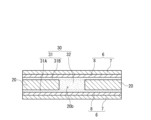
- FIG. 1 is a cross-sectional view illustrating a schematic example of an electrolytic capacitor according to an embodiment of the present disclosure.
- 2 is an enlarged schematic cross-sectional view of a main portion near a metal foil disposed between adjacent capacitor elements of the element laminate of the electrolytic capacitor shown in FIG. 1 .
- 2 is an enlarged schematic cross-sectional view of a main portion in the vicinity of a metal foil disposed at one end of the element laminate of the electrolytic capacitor shown in FIG. 1 .
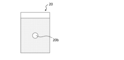
- FIG. 2 is a top view showing a schematic diagram of an example of a metal foil having one through-hole having a circular cross section.
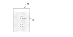
- FIG. 2 is a top view showing a schematic diagram of an example of a metal foil having two through holes each having a circular cross section.
- FIG. 2 is a top view showing a schematic diagram of an example of a metal foil having five through holes each having a circular cross section.
- FIG. 2 is a top view showing a schematic diagram of an example of a metal foil having three through holes each having a linear cross section.
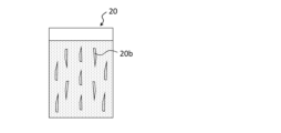
- FIG. 2 is a top view showing a schematic diagram of an example of a metal foil having five through holes each having a linear cross section.
- FIG. 2 is a top view showing a schematic diagram of an example of a metal foil having seven through holes each having a linear cross section.
- FIG. 2 is a top view showing a schematic diagram of an example of a metal foil having nine through holes each having a linear cross section.
- FIG. 2 is a top view showing a schematic diagram of an example of a metal foil having eleven through-holes each having a linear cross section.
- the embodiments of the present disclosure are described using examples, but the present disclosure is not limited to the examples described below.
- specific numerical values and materials may be exemplified, but other numerical values and materials may be applied as long as the effects of the present disclosure are obtained.
- the expression "numerical value A to numerical value B" includes numerical value A and numerical value B and can be read as "numerical value A or more and numerical value B or less.”
- any of the exemplified lower limits and any of the exemplified upper limits can be arbitrarily combined as long as the lower limit is not equal to or greater than the upper limit.
- one of the materials may be selected and used alone, or two or more of the materials may be used in combination.
- the present disclosure encompasses a combination of the features described in two or more claims arbitrarily selected from the multiple claims described in the appended claims.
- the features described in two or more claims arbitrarily selected from the multiple claims described in the appended claims may be combined, provided that no technical contradiction arises.
- the conductive adhesive layer may be formed, for example, by applying a conductive adhesive to one main surface of the metal foil (the area to be attached to the cathode portion), placing a capacitor element (cathode portion) on top of the conductive adhesive, and then filling the through-hole on the other main surface of the metal foil with the conductive adhesive through the opening of the through-hole. If a capacitor element (cathode portion) is then separately placed on the other main surface of the metal foil, the conductive adhesive may be applied on the conductive adhesive filled in the other main surface of the metal foil and the through-hole, and the capacitor element (cathode portion) may be placed on top of the conductive adhesive.
- the separation layer may contain, for example, a resin, and may be one of the examples of the exterior body described below.
- the dielectric layer formed in the porous portion of the first part may be compressed and densified to provide insulation.
- Laminated samples a1 to a4 had a larger breaking load and higher adhesive strength than laminated sample b1.
- laminated samples a1 to a3 which had a through-hole ratio of 15% or less, had excellent adhesive strength.
Landscapes
- Engineering & Computer Science (AREA)
- Power Engineering (AREA)
- Microelectronics & Electronic Packaging (AREA)
- Chemical & Material Sciences (AREA)
- Materials Engineering (AREA)
- Fixed Capacitors And Capacitor Manufacturing Machines (AREA)
Abstract
This electrolytic capacitor comprises: a capacitor element that is provided with a positive electrode part and a negative electrode part; an exterior body that seals the capacitor element; a metal foil that is electrically connected to the negative electrode part; a first external electrode that is electrically connected to the metal foil; and a conductive adhesive layer. The metal foil has a through hole that passes therethrough in the thickness direction. The conductive adhesive layer includes a first layer that is between the negative electrode part and a main surface of the metal foil, and a second layer that is filled in the through hole. The first layer and the second layer are integrated with each other. The metal foil has a first end surface that is exposed from the exterior body. The first end surface is electrically connected to the first external electrode.
Description
本開示は、電解コンデンサに関する。
This disclosure relates to electrolytic capacitors.
電解コンデンサは、コンデンサ素子と、コンデンサ素子を封止する外装体と、コンデンサ素子と電気的に接続される外部電極と、を備える。コンデンサ素子は、陽極部と、陰極部とを備える。陰極部は、導電性接着層を介して金属箔と密着している。金属箔は、外装体から露出する端面を有し、当該端面は、陰極側の外部電極と電気的に接続している。
The electrolytic capacitor comprises a capacitor element, an exterior body that seals the capacitor element, and an external electrode that is electrically connected to the capacitor element. The capacitor element comprises an anode portion and a cathode portion. The cathode portion is in close contact with the metal foil via a conductive adhesive layer. The metal foil has an end face that is exposed from the exterior body, and the end face is electrically connected to the cathode-side external electrode.
特許文献1は、「多孔質層を表面に有する弁作用金属基体と、前記多孔質層の表面に形成された誘電体層と、前記誘電体層上に設けられた固体電解質層とを有するユニットが複数個積層された固体電解コンデンサであって、積層されたユニットの間に導電体層が存在し、前記導電体層のうち少なくとも一つは金属箔を含み、前記ユニット及び前記導電体層は、外装樹脂により封止されており、前記弁作用金属基体の陽極部側端面は、固体電解コンデンサの一端面において外装樹脂の表面に形成された陽極外部電極と直接接続されており、前記金属箔は、固体電解コンデンサの他端面において外装樹脂の表面に形成された陰極外部電極と直接接続されていることを特徴とする固体電解コンデンサ」を開示している。
Patent Document 1 discloses a solid electrolytic capacitor in which "a plurality of units are stacked, each unit having a valve action metal substrate having a porous layer on its surface, a dielectric layer formed on the surface of the porous layer, and a solid electrolyte layer provided on the dielectric layer, a conductive layer is present between the stacked units, at least one of the conductive layers includes metal foil, the units and the conductive layer are sealed with an exterior resin, the anode side end face of the valve action metal substrate is directly connected to an anode external electrode formed on the surface of the exterior resin at one end face of the solid electrolytic capacitor, and the metal foil is directly connected to a cathode external electrode formed on the surface of the exterior resin at the other end face of the solid electrolytic capacitor."
また、特許文献1は、「前記金属箔を含む導電体層は、前記固体電解質層上に設けられたカーボン層と、前記カーボン層上に設けられた導電性接着剤層と、前記導電性接着剤層上に設けられた金属箔とからなる」ことを開示している。
Patent document 1 also discloses that "the conductive layer containing the metal foil is composed of a carbon layer provided on the solid electrolyte layer, a conductive adhesive layer provided on the carbon layer, and a metal foil provided on the conductive adhesive layer."
導電性接着層を介した金属箔とコンデンサ素子(陰極部)との間の接着強度が低い。よって、金属箔とコンデンサ素子との間の剥離(以下、「積層剥離」とも称する。)が生じて接触抵抗が増大し易い。また、コンデンサ素子を封止する際にコンデンサ素子と金属箔とのずれ(以下、「積層ずれ」とも称する。)が生じ易い。その結果、電解コンデンサの信頼性が低下する。
The adhesive strength between the metal foil and the capacitor element (cathode) via the conductive adhesive layer is low. This means that peeling between the metal foil and the capacitor element (hereinafter also referred to as "lamination peeling") is likely to occur, increasing the contact resistance. In addition, misalignment between the capacitor element and the metal foil (hereinafter also referred to as "lamination misalignment") is likely to occur when sealing the capacitor element. As a result, the reliability of the electrolytic capacitor is reduced.
本開示の一側面は、陽極部および陰極部を備えるコンデンサ素子と、前記コンデンサ素子を封止する外装体と、前記陰極部と電気的に接続する金属箔と、前記金属箔と電気的に接続する第1外部電極と、導電性接着層と、を備え、
前記金属箔は、厚み方向に貫通する貫通穴を有し、前記導電性接着層は、前記陰極部と前記金属箔の主面との間に介在する第1層と、前記貫通穴に充填される第2層と、を含み、前記第1層と前記第2層とは、一体化されており、前記金属箔は、前記外装体から露出する第1端面を有し、前記第1端面は、前記第1外部電極と電気的に接続している、電解コンデンサに関する。 One aspect of the present disclosure provides a capacitor including a capacitor element having an anode portion and a cathode portion, an exterior body sealing the capacitor element, a metal foil electrically connected to the cathode portion, a first external electrode electrically connected to the metal foil, and a conductive adhesive layer;
The present invention relates to an electrolytic capacitor, wherein the metal foil has a through hole penetrating in the thickness direction, the conductive adhesive layer includes a first layer interposed between the cathode portion and a main surface of the metal foil and a second layer filled in the through hole, the first layer and the second layer being integrated, and the metal foil has a first end face exposed from the outer casing, and the first end face is electrically connected to the first external electrode.
本開示によれば、電解コンデンサの信頼性の低下を抑制することができる。
This disclosure makes it possible to prevent a decrease in the reliability of electrolytic capacitors.
本発明の新規な特徴を添付の請求の範囲に記述するが、本発明は、構成および内容の両方に関し、本発明の他の目的および特徴と併せ、図面を照合した以下の詳細な説明によりさらによく理解されるであろう。
The novel features of the present invention are set forth in the appended claims, but the present invention, both in terms of structure and content, together with other objects and features of the present invention, will be better understood from the following detailed description taken in conjunction with the drawings.
以下では、本開示の実施形態について例を挙げて説明するが、本開示は以下で説明する例に限定されない。以下の説明では、具体的な数値や材料を例示する場合があるが、本開示の効果が得られる限り、他の数値や材料を適用してもよい。この明細書において、「数値A~数値B」という記載は、数値Aおよび数値Bを含み、「数値A以上で数値B以下」と読み替えることが可能である。以下の説明において、特定の物性や条件などに関する数値の下限と上限とを例示した場合、下限が上限以上とならない限り、例示した下限のいずれかと例示した上限のいずれかを任意に組み合わせることができる。複数の材料が例示される場合、その中から1種を選択して単独で用いてもよく、2種以上を組み合わせて用いてもよい。
Below, the embodiments of the present disclosure are described using examples, but the present disclosure is not limited to the examples described below. In the following description, specific numerical values and materials may be exemplified, but other numerical values and materials may be applied as long as the effects of the present disclosure are obtained. In this specification, the expression "numerical value A to numerical value B" includes numerical value A and numerical value B and can be read as "numerical value A or more and numerical value B or less." In the following description, when a lower limit and an upper limit of a numerical value related to a specific physical property or condition are exemplified, any of the exemplified lower limits and any of the exemplified upper limits can be arbitrarily combined as long as the lower limit is not equal to or greater than the upper limit. When multiple materials are exemplified, one of the materials may be selected and used alone, or two or more of the materials may be used in combination.
また、本開示は、添付の請求の範囲に記載の複数の請求項から任意に選択される2つ以上の請求項に記載の事項の組み合わせを包含する。つまり、技術的な矛盾が生じない限り、添付の請求の範囲に記載の複数の請求項から任意に選択される2つ以上の請求項に記載の事項を組み合わせることができる。
In addition, the present disclosure encompasses a combination of the features described in two or more claims arbitrarily selected from the multiple claims described in the appended claims. In other words, the features described in two or more claims arbitrarily selected from the multiple claims described in the appended claims may be combined, provided that no technical contradiction arises.
本開示の実施形態に係る電解コンデンサは、陽極部および陰極部を備えるコンデンサ素子と、コンデンサ素子を封止する外装体と、陰極部と電気的に接続する金属箔と、金属箔と電気的に接続する第1外部電極と、導電性接着層と、を備える。金属箔は、外装体から露出する第1端面を有し、第1端面は、第1外部電極と電気的に接続している。金属箔は、厚み方向に貫通する貫通穴を有する。導電性接着層は、陰極部と金属箔の主面との間に介在する第1層と、貫通穴に充填される第2層と、を含む。第1層と第2層とは、一体化されている。電解コンデンサは、コンデンサ素子を1つ含んでもよく、複数のコンデンサ素子を含んでもよい。第1層は、金属箔の主面および貫通穴に充填される第2層の上に形成される。
An electrolytic capacitor according to an embodiment of the present disclosure includes a capacitor element having an anode portion and a cathode portion, an exterior body sealing the capacitor element, a metal foil electrically connected to the cathode portion, a first external electrode electrically connected to the metal foil, and a conductive adhesive layer. The metal foil has a first end face exposed from the exterior body, and the first end face is electrically connected to the first external electrode. The metal foil has a through hole penetrating in the thickness direction. The conductive adhesive layer includes a first layer interposed between the cathode portion and a main surface of the metal foil, and a second layer filled in the through hole. The first layer and the second layer are integrated. The electrolytic capacitor may include one capacitor element or may include multiple capacitor elements. The first layer is formed on the main surface of the metal foil and on the second layer filled in the through hole.
貫通穴に充填された第2層による接着効果およびアンカー効果が相俟って、金属箔および陰極部と接着層(第1層)との間の密着強度が向上する。これにより、金属箔と陰極部との間の接着強度の低下が抑制され、接触抵抗の増大が抑制され、積層剥離および積層ずれが抑制され、積層剥離および積層ずれに起因する電解コンデンサの信頼性の低下が抑制される。信頼性の低下は、性能の低下、性能のばらつきの増大などを含む。
The adhesive effect and anchor effect of the second layer filled in the through hole combine to improve the adhesion strength between the metal foil and the cathode part and the adhesive layer (first layer). This prevents a decrease in adhesive strength between the metal foil and the cathode part, prevents an increase in contact resistance, prevents delamination and lamination misalignment, and prevents a decrease in the reliability of the electrolytic capacitor due to delamination and lamination misalignment. Decreases in reliability include a decrease in performance and an increase in performance variability.
貫通穴の全体に第2層が充填されていることが望ましいが、第2層による効果を損なわない範囲で、貫通穴の一部に第2層が充填されていない部分(空隙)が含まれていてもよい。貫通穴への第2層の充填率は、55%以上であってもよく、75%以上であってもよい。貫通穴への第2層の充填率とは、金属箔の厚さ方向の断面(貫通穴を有する断面)における、貫通穴が占める領域の面積に対する第2層が占める領域の面積の割合である。すなわち、上記の断面において、貫通穴が占める領域の面積をS0とし、第2層が占める領域の面積をS1とするとき、(S1/S0)×100により求められる。複数の貫通穴のそれぞれに第2層が充填されている場合、貫通穴の総数の60%以上(好ましくは80%以上)において、第2層の充填率が90%以上であることが望ましい。
It is desirable that the second layer fills the entire through hole, but a portion of the through hole may contain a portion (a gap) that is not filled with the second layer, as long as the effect of the second layer is not impaired. The filling rate of the through hole with the second layer may be 55% or more, or 75% or more. The filling rate of the through hole with the second layer is the ratio of the area of the area occupied by the through hole in a cross section (cross section having the through hole) in the thickness direction of the metal foil to the area of the area occupied by the second layer. In other words, when the area of the area occupied by the through hole in the above cross section is S0 and the area of the area occupied by the second layer is S1, it is calculated by (S1/S0) x 100. When each of a plurality of through holes is filled with the second layer, it is desirable that the filling rate of the second layer is 90% or more in 60% or more (preferably 80% or more) of the total number of through holes.
電解コンデンサは、コンデンサ素子を複数積層した素子積層体を備えてもよい。この場合、金属箔は、複数のコンデンサ素子の少なくとも1つに配置されている。この場合、金属箔は、互いに隣り合うコンデンサ素子同士の間に配置されていることが好ましい。すなわち、互いに隣り合うコンデンサ素子間で、1つの金属箔を共有していることが好ましい。この場合、第1層は、金属箔の両方の主面に形成されている。すなわち、第1層は、互いに隣り合うコンデンサ素子同士のうちの一方のコンデンサ素子の陰極部と金属箔の一方の主面との間に介在する第1A層と、互いに隣り合うコンデンサ素子のうちの他方のコンデンサ素子の陰極部と金属箔の他方の主面との間に介在する第1B層と、を含む。第1A層および第1B層と、第2層とは、一体化されている。
The electrolytic capacitor may include an element stack in which a plurality of capacitor elements are stacked. In this case, the metal foil is disposed in at least one of the plurality of capacitor elements. In this case, it is preferable that the metal foil is disposed between adjacent capacitor elements. In other words, it is preferable that one metal foil is shared between adjacent capacitor elements. In this case, the first layer is formed on both main surfaces of the metal foil. In other words, the first layer includes a first A layer interposed between the cathode portion of one of the adjacent capacitor elements and one main surface of the metal foil, and a first B layer interposed between the cathode portion of the other of the adjacent capacitor elements and the other main surface of the metal foil. The first A layer and the first B layer are integrated with the second layer.
互いに隣り合うコンデンサ素子間に金属箔を配置する場合、互いに隣り合うコンデンサ素子同士の間に、第1A層と第2層と第1B層とが介在する領域が形成される。第1A層および第1B層は、第2層を介して一体化されている。これにより、コンデンサ素子同士の間の接着強度が更に向上する。第2層によるアンカー効果が、第1A層および第1B層の両方に対して効率的に発揮される。
When metal foil is placed between adjacent capacitor elements, an area is formed between the adjacent capacitor elements where the first A layer, the second layer, and the first B layer are interposed. The first A layer and the first B layer are integrated via the second layer. This further improves the adhesive strength between the capacitor elements. The anchor effect of the second layer is efficiently exerted on both the first A layer and the first B layer.
また、互いに隣り合うコンデンサ素子間に金属箔を配置する場合、素子積層体内で生じたガスが金属箔の貫通穴を経由して排気され、ガスの発生量の増大に伴う電解コンデンサの積層方向の膨れが抑制され、当該膨れに伴う性能低下(例えばESRの上昇)および性能のばらつきが抑制される。ガスは、特に、貫通穴の第2層が充填されない領域(空隙)を移動し易い。当該ガスは、導電性接着層の形成時の加熱による硬化処理、リフロー処理などにより、電解コンデンサが高温に曝される場合に発生し易い。
In addition, when metal foil is placed between adjacent capacitor elements, gas generated within the element stack is exhausted through the through holes in the metal foil, suppressing swelling of the electrolytic capacitor in the stacking direction due to increased gas generation, and suppressing performance degradation (e.g., increased ESR) and performance variation due to such swelling. Gas is particularly likely to move through areas (gaps) where the second layer of the through holes is not filled. Such gas is likely to be generated when the electrolytic capacitor is exposed to high temperatures due to curing treatment by heating when forming the conductive adhesive layer, reflow treatment, etc.
(貫通穴)
金属箔は、厚み方向に貫通する貫通穴を、1つまたは複数有する。貫通穴の個数は、例えば、1~500個である。貫通穴の最大径は、例えば、0.01mm以上、2mm以下である。貫通穴の断面の面積は、例えば、78μm2以上、3.14mm2以下である。複数の貫通穴が規則的に設けられていてもよい。複数の貫通穴は、格子状(例えば、千鳥格子状、正方格子状)に設けられていてもよい。 (Through hole)
The metal foil has one or more through holes penetrating in the thickness direction. The number of through holes is, for example, 1 to 500. The maximum diameter of the through hole is, for example, 0.01 mm or more and 2 mm or less. The cross-sectional area of the through hole is, for example, 78 μm2 or more and 3.14 mm2 or less. The multiple through holes may be provided regularly. The multiple through holes may be provided in a lattice pattern (for example, a houndstooth lattice pattern, a square lattice pattern).
第2層の形成による接着強度の向上、第1層による陰極部との密着領域の確保、および金属箔の強度確保などの観点から、金属箔を、その主面の法線方向から見たとき、金属箔(陰極部に密着させる領域)に占める貫通穴の面積の割合は、0.04%以上、15%以下が好ましく、0.1%以上、10%以下がより好ましい。陰極部に密着させる領域とは、第1層を形成する領域とも言える。貫通穴を複数有する場合、貫通穴の面積は、複数の貫通穴の合計面積である。
From the viewpoints of improving the adhesive strength by forming the second layer, ensuring an area of adhesion with the cathode part by the first layer, and ensuring the strength of the metal foil, when the metal foil is viewed in the normal direction of its main surface, the ratio of the area of the through holes to the metal foil (area that is in close contact with the cathode part) is preferably 0.04% or more and 15% or less, and more preferably 0.1% or more and 10% or less. The area that is in close contact with the cathode part can also be said to be the area where the first layer is formed. When there are multiple through holes, the area of the through holes is the total area of the multiple through holes.
貫通穴の面積の割合が0.04%以上(もしくは0.1%以上)である場合、第2層による効果が得られ易い。貫通穴の面積の割合が15%以下(もしくは10%以下)である場合、金属箔による導電性が十分に確保される。
If the area ratio of the through holes is 0.04% or more (or 0.1% or more), the effect of the second layer is easily obtained. If the area ratio of the through holes is 15% or less (or 10% or less), the conductivity of the metal foil is sufficiently ensured.
金属箔を、その主面の法線方向から見たとき、貫通穴の形状は、円形状、楕円形状、多角形状、または線形状であってもよい。貫通穴は、形状によっては、打ち抜き加工により形成してもよい。線形状の貫通穴は、カッターナイフなどを用いて形成される幅が細長い形状である。線形状は、直線状でもよく、曲線状でもよい。多角形状としては、三角形状、四角形状などが挙げられる。貫通穴を有する金属箔としては、例えば、図4~図11に示す、貫通穴20bを有する金属箔20が挙げられる。なお、図4~図11中の網掛け部分は、陰極部に密着させる領域である。
When the metal foil is viewed in the normal direction of its main surface, the shape of the through hole may be circular, elliptical, polygonal, or linear. Depending on the shape, the through hole may be formed by punching. A linear through hole is an elongated shape formed using a cutter knife or the like. The linear shape may be straight or curved. Examples of polygonal shapes include triangular and rectangular shapes. An example of a metal foil having a through hole is metal foil 20 having a through hole 20b shown in Figures 4 to 11. The shaded areas in Figures 4 to 11 are areas that are brought into close contact with the cathode part.
貫通穴の形成方法によっては、金属箔の主面の粗さが大きくなることがある。例えば、カッターナイフなどにより線形状の貫通穴を形成する場合、貫通穴の周縁部に凸部が形成され得る。貫通穴を有する金属箔の主面の面粗さSaは、例えば、10μm以上、200μm以下である。なお、「面粗さSa」は、JIS B 0681-2:2018に規定される三次元表面性状パラメータの一つであり、算術平均高さを表す。
Depending on the method for forming the through holes, the roughness of the main surface of the metal foil may increase. For example, when forming linear through holes using a cutter knife, a convex portion may be formed on the periphery of the through hole. The surface roughness Sa of the main surface of the metal foil having the through holes is, for example, 10 μm or more and 200 μm or less. Note that "surface roughness Sa" is one of the three-dimensional surface property parameters defined in JIS B 0681-2:2018, and represents the arithmetic mean height.
(金属箔)
貫通穴の形成し易さ、強度、導電性などの観点から、金属箔は、アルミニウム、アルミニウム合金、銅、または銅合金を含むことが好ましい。金属箔の主面は、エッチング処理などにより粗面化されてもよい。金属箔は、主面に被覆層を有してもよい。被覆層は、金属箔の一方の主面に形成されてもよく、両方の主面に形成されてもよい。被覆層は、例えば、金属箔とは異なる材料(金属、金属化合物、非金属など)を含む。 (Metal foil)
From the viewpoints of ease of forming through holes, strength, conductivity, etc., the metal foil preferably contains aluminum, an aluminum alloy, copper, or a copper alloy. The main surface of the metal foil may be roughened by etching or the like. The metal foil may have a coating layer on the main surface. The coating layer may be formed on one or both main surfaces of the metal foil. The coating layer contains, for example, a material (metal, metal compound, nonmetal, etc.) different from the metal foil.
被覆層を構成する材料としては、例えば、金属(チタン、ニッケルなど)、チタン化合物などの金属化合物(窒化物、炭化物、炭窒化物、酸化物など)、炭素質材料などが挙げられる。金属酸化物は、化成処理により形成されてもよい。被覆層は、これらの材料を一種含んでもよく、二種以上含んでもよい。被覆層は、単層構造であってもよく、多層構造であってもよい。
Materials constituting the coating layer include, for example, metals (titanium, nickel, etc.), metal compounds such as titanium compounds (nitrides, carbides, carbonitrides, oxides, etc.), and carbonaceous materials. Metal oxides may be formed by chemical conversion treatment. The coating layer may contain one or more of these materials. The coating layer may have a single layer structure or a multilayer structure.
被覆層は、チタン層、ニッケル層、チタン窒化物層、チタン炭化物層、チタン炭窒化物層、チタン酸化物層、およびカーボン層からなる群より選択される少なくとも1層により構成されていることが好ましい。この場合、性能低下(例えばESRの上昇)が抑制され易く、性能ばらつきが低減され易い。
The coating layer is preferably composed of at least one layer selected from the group consisting of a titanium layer, a nickel layer, a titanium nitride layer, a titanium carbide layer, a titanium carbonitride layer, a titanium oxide layer, and a carbon layer. In this case, performance degradation (e.g., an increase in ESR) is easily suppressed, and performance variation is easily reduced.
被覆層は、材料によっては、気相法、焼成法などにより形成されてもよい。被覆層を構成する材料が、金属箔に直接固着され、高い導電性が得られる。気相法としては、蒸着(真空蒸着、電子ビーム蒸着、アークプラズマ蒸着など)、スパッタリング法、CVD法などが挙げられる。
Depending on the material, the coating layer may be formed by a gas phase method, a baking method, etc. The material that constitutes the coating layer is directly adhered to the metal foil, resulting in high conductivity. Gas phase methods include deposition (vacuum deposition, electron beam deposition, arc plasma deposition, etc.), sputtering, and CVD.
金属箔の厚みは、0.1μm以上、100μm以下であってもよく、1μm以上、50μm以下であってもよい。被覆層の厚みは、金属箔の片方の主面あたり、0.5μm以上、10μm以下であってもよく、1μm以上、5μm以下であってもよい。
The thickness of the metal foil may be 0.1 μm or more and 100 μm or less, or 1 μm or more and 50 μm or less. The thickness of the coating layer may be 0.5 μm or more and 10 μm or less, or 1 μm or more and 5 μm or less, per main surface of the metal foil.
(導電性接着層)
導電性接着層は、導電性粒子と、樹脂(バインダー樹脂)と、を含むことが好ましい。導電性粒子は、カーボン粒子および金属粒子からなる群より選択される少なくとも1種を含むことが好ましい。金属粒子としては、銀粒子、銅粒子などが挙げられる。樹脂は、熱可塑性樹脂および硬化性樹脂の硬化物の少なくとも一方を含んでもよい。 (Conductive adhesive layer)
The conductive adhesive layer preferably contains conductive particles and a resin (binder resin). The conductive particles preferably contain at least one selected from the group consisting of carbon particles and metal particles. Examples of the metal particles include silver particles and copper particles. The resin may contain at least one of a thermoplastic resin and a cured product of a curable resin.
導電性接着層の形成に用いられる導電性接着剤は、例えば、導電性粒子と、熱可塑性樹脂および硬化性樹脂の少なくとも一方の樹脂材料と、を含む。導電性接着剤に用いられる樹脂材料としては、例えば、エポキシ樹脂、アクリル樹脂、ポリイミド樹脂、ポリアミド樹脂、ポリウレタン樹脂、ポリエステル樹脂、フッ素樹脂、ビニル樹脂、ポリオレフィン樹脂、フェノキシ樹脂、ゴム状材料などが挙げられる。エポキシ樹脂としては、ビスフェノールF型エポキシ樹脂、ビスフェノールA型エポキシ樹脂、あるいは、これらを混合したものを用いることができる。また、エポキシ樹脂は、多官能エポキシ樹脂を含んでもよい。多官能エポキシ樹脂としては、テトラフェニロールエタン型樹脂を用いることができる。導電性接着剤は、硬化剤、重合開始剤などの他の材料を含んでもよい。導電性接着剤は、溶剤を含んでもよい。
The conductive adhesive used to form the conductive adhesive layer includes, for example, conductive particles and at least one of a thermoplastic resin and a curable resin. Examples of the resin material used in the conductive adhesive include epoxy resin, acrylic resin, polyimide resin, polyamide resin, polyurethane resin, polyester resin, fluororesin, vinyl resin, polyolefin resin, phenoxy resin, and rubber-like materials. As the epoxy resin, bisphenol F type epoxy resin, bisphenol A type epoxy resin, or a mixture of these can be used. The epoxy resin may also include a polyfunctional epoxy resin. As the polyfunctional epoxy resin, tetraphenylolethane type resin can be used. The conductive adhesive may include other materials such as a curing agent and a polymerization initiator. The conductive adhesive may also include a solvent.
導電性接着層は、例えば、導電性接着剤を金属箔の一方の主面(陰極部に密着させる領域)に塗布し、その上にコンデンサ素子(陰極部)を配置し、その後、金属箔の他方の主面側の貫通穴の開口より当該貫通穴内に導電性接着剤を充填することにより形成してもよい。その後、金属箔の他方の主面にも別途コンデンサ素子(陰極部)を配置する場合、さらに、金属箔の他方の主面および貫通穴に充填された導電性接着剤の上に導電性接着剤を塗布し、その上にコンデンサ素子(陰極部)を配置してもよい。
The conductive adhesive layer may be formed, for example, by applying a conductive adhesive to one main surface of the metal foil (the area to be attached to the cathode portion), placing a capacitor element (cathode portion) on top of the conductive adhesive, and then filling the through-hole on the other main surface of the metal foil with the conductive adhesive through the opening of the through-hole. If a capacitor element (cathode portion) is then separately placed on the other main surface of the metal foil, the conductive adhesive may be applied on the conductive adhesive filled in the other main surface of the metal foil and the through-hole, and the capacitor element (cathode portion) may be placed on top of the conductive adhesive.
また、導電性接着剤をコンデンサ素子の一方の主面側の陰極部に塗布し、その上に金属箔を配置し、その後、導電性接着剤を当該コンデンサ素子の他方の主面側の陰極部に塗布し、その上に別途金属箔を配置してもよい。その後、金属箔の上からコンデンサ素子に荷重をかけて、陰極部に塗布された導電接着剤の一部を貫通穴に入り込ませてもよい。このようにして、導電性接着層を形成してもよい。
Alternatively, a conductive adhesive may be applied to the cathode portion on one main surface of the capacitor element, metal foil may be placed on top of that, and then a conductive adhesive may be applied to the cathode portion on the other main surface of the capacitor element, with separate metal foil placed on top of that. A load may then be applied to the capacitor element from above the metal foil, causing part of the conductive adhesive applied to the cathode portion to penetrate into the through hole. In this manner, a conductive adhesive layer may be formed.
以下、電解コンデンサについて、詳述する。
コンデンサ素子は、陽極部と、陰極部とを備える。陽極部は、例えば、一方の端部(第1端部とも称する。)を含む第1部分と、一方の端部とは反対側の他方の端部(第2端部とも称する。)を含む第2部分とを含む陽極体である。陰極部は、陽極体の第2部分に形成される。陽極体は少なくとも第2部分の表面に誘電体層を有する。 The electrolytic capacitor will be described in detail below.
The capacitor element includes an anode portion and a cathode portion. The anode portion is, for example, an anode body including a first portion including one end (also referred to as a first end) and a second portion including the other end (also referred to as a second end) opposite to the one end. The cathode portion is formed in the second portion of the anode body. The anode body has a dielectric layer on at least a surface of the second portion.
(陽極体)
陽極体は、例えば、弁作用金属、弁作用金属を含む合金、および弁作用金属を含む化合物(金属間化合物など)を含んでもよい。これらの材料は一種を単独でまたは二種以上を組み合わせて使用してもよい。弁作用金属としては、アルミニウム、タンタル、ニオブ、チタンなどが挙げられる。陽極体は、弁作用金属、弁作用金属を含む合金、または弁作用金属を含む化合物の箔(陽極箔)であってもよく、弁作用金属、弁作用金属を含む合金、または弁作用金属を含む化合物の粒子の成形体(多孔質成形体)またはその焼結体(多孔質焼結体)であってもよい。 (Anode body)
The anode body may contain, for example, a valve metal, an alloy containing a valve metal, and a compound containing a valve metal (such as an intermetallic compound). These materials may be used alone or in combination of two or more. Examples of the valve metal include aluminum, tantalum, niobium, and titanium. The anode body may be a foil (anode foil) of a valve metal, an alloy containing a valve metal, or a compound containing a valve metal, or may be a molded body (porous molded body) or a sintered body (porous sintered body) of particles of a valve metal, an alloy containing a valve metal, or a compound containing a valve metal.
陽極体として陽極箔を用いる場合、通常、表面積を増やすため、陽極箔の少なくとも第2部分の表面には、多孔質部が形成される。このような陽極箔は、芯部と、芯部の表面に形成された多孔質部とを有する。多孔質部は、例えば、陽極箔の表面に凹凸を形成することにより形成される。多孔質部を有する陽極箔は、例えば、陽極箔の少なくとも第2部分の表面をエッチング(電解エッチングなど)などにより粗面化することによって形成してもよい。第1部分の表面に所定のマスキング部材を配置した後、エッチング処理などの粗面化処理を行うことも可能である。一方で、陽極箔の表面の全面をエッチング処理などにより粗面化処理することも可能である。前者の場合、第1部分の表面には多孔質部を有さず、第2部分の表面に多孔質部を有する陽極箔が得られる。後者の場合、第2部分の表面に加え、第1部分の表面にも多孔質部が形成される。エッチング処理としては、公知の手法を用いればよく、例えば、電解エッチングが挙げられる。マスキング部材は、特に限定されず、導電性材料を含む導電体であってもよいが、樹脂などの絶縁体が好ましい。マスキング部材は、固体電解質層の形成前に取り除かれる。
When an anode foil is used as an anode body, a porous portion is usually formed on at least the second portion of the anode foil in order to increase the surface area. Such an anode foil has a core and a porous portion formed on the surface of the core. The porous portion is formed, for example, by forming irregularities on the surface of the anode foil. An anode foil having a porous portion may be formed, for example, by roughening the surface of at least the second portion of the anode foil by etching (electrolytic etching, etc.). It is also possible to perform a roughening process such as an etching process after placing a predetermined masking member on the surface of the first portion. On the other hand, it is also possible to roughen the entire surface of the anode foil by etching or the like. In the former case, an anode foil is obtained that does not have a porous portion on the surface of the first portion and has a porous portion on the surface of the second portion. In the latter case, a porous portion is formed on the surface of the first portion in addition to the surface of the second portion. As the etching process, a known method may be used, for example, electrolytic etching. The masking member is not particularly limited and may be a conductor containing a conductive material, but an insulator such as a resin is preferable. The masking material is removed before the solid electrolyte layer is formed.
陽極箔の表面の全面を粗面化処理する場合、第1部分の表面に多孔質部を有する。この場合、多孔質部と外装体との接触部分を通じて固体電解コンデンサ内部に空気が侵入することを抑制する観点から、第1部分に形成された多孔質部の少なくとも一部を、予め、除去したり、圧縮して多孔質部の孔をつぶしたりしておいてもよい。これによって、空気の侵入による電解コンデンサの信頼性の低下を抑制できる。
When the entire surface of the anode foil is roughened, the surface of the first portion has a porous portion. In this case, in order to prevent air from entering the solid electrolytic capacitor through the contact portion between the porous portion and the exterior body, at least a portion of the porous portion formed in the first portion may be removed in advance or compressed to crush the pores of the porous portion. This makes it possible to prevent a decrease in the reliability of the electrolytic capacitor due to air entering the electrolytic capacitor.
複数のコンデンサ素子を積層する場合、コンデンサ素子の陽極体の第1端部を束ねて、リードと接続して、外部電極と電気的に接続してもよい。しかし、束ねずに複数の第1端部の端面をそれぞれ外装体の外面から露出させて、外部電極と電気的に接続させてもよい。
When stacking multiple capacitor elements, the first ends of the anode bodies of the capacitor elements may be bundled together and connected to a lead for electrical connection to an external electrode. However, instead of bundling, the end faces of the multiple first ends may each be exposed from the outer surface of the exterior body and electrically connected to an external electrode.
なお、外装体の外面とは、外装体の外形を形作る表面である。例えば、コンデンサ素子が基板とともに外装体で封止された封止物が直方体または立方体などの形状を有する場合、1つの表面(例えば、底面)が基板の表面に相当し、基板の表面以外の残りの5つの表面(例えば、側面、天面など)が外装体の外面に相当することがある。
The outer surface of the exterior body is the surface that forms the outer shape of the exterior body. For example, if the sealed object in which the capacitor element is sealed together with the substrate in the exterior body has a rectangular or cubic shape, one surface (e.g., the bottom surface) may correspond to the surface of the substrate, and the remaining five surfaces other than the substrate surface (e.g., the sides, top surface, etc.) may correspond to the outer surface of the exterior body.
(誘電体層)
誘電体層は、例えば、陽極体の少なくとも第2部分の表面の弁作用金属を、化成処理などにより陽極酸化することで形成される。誘電体層は弁作用金属の酸化物を含む。例えば、弁作用金属としてアルミニウムを用いた場合の誘電体層は酸化アルミニウムを含む。誘電体層は、少なくとも多孔質部が形成されている第2部分の表面(多孔質部の孔の内壁面を含む)に沿って形成される。なお、誘電体層の形成方法はこれに限定されず、第2部分の表面に、誘電体として機能する絶縁性の層を形成できればよい。誘電体層は、第1部分の表面(例えば、第1部分の表面の多孔質部)にも形成されてもよい。 (Dielectric Layer)
The dielectric layer is formed, for example, by anodizing the valve metal on at least the surface of the second portion of the anode body by chemical conversion treatment or the like. The dielectric layer contains an oxide of the valve metal. For example, when aluminum is used as the valve metal, the dielectric layer contains aluminum oxide. The dielectric layer is formed along at least the surface of the second portion in which the porous portion is formed (including the inner wall surface of the hole of the porous portion). Note that the method of forming the dielectric layer is not limited to this, and it is sufficient if an insulating layer that functions as a dielectric can be formed on the surface of the second portion. The dielectric layer may also be formed on the surface of the first portion (for example, the porous portion on the surface of the first portion).
化成処理は、例えば、陽極体を化成液中に浸漬することにより、陽極体の表面に化成液を含浸させ、陽極体をアノードとして、化成液中に浸漬したカソードとの間に電圧を印加することにより行うことができる。陽極体の表面に多孔質部を有する場合、誘電体層は、多孔質部の表面の凹凸形状に沿って形成される。
The chemical conversion treatment can be carried out, for example, by immersing the anode body in a chemical conversion solution, thereby impregnating the surface of the anode body with the chemical conversion solution, and applying a voltage between the anode body as the anode and a cathode immersed in the chemical conversion solution. If the anode body has a porous portion on its surface, the dielectric layer is formed to conform to the uneven shape of the surface of the porous portion.
(陰極部)
陰極部は、誘電体層を有する陽極体の第2部分に形成される。分離層の第2部分側の表面を陰極部が覆っている場合もある。 (Cathode)
The cathode part is formed on the second part of the anode body having the dielectric layer, and may cover the surface of the separation layer facing the second part.
陰極部は、誘電体層を有する陽極体の第2部分に形成される。分離層の第2部分側の表面を陰極部が覆っている場合もある。 (Cathode)
The cathode part is formed on the second part of the anode body having the dielectric layer, and may cover the surface of the separation layer facing the second part.
陰極部は、誘電体層の少なくとも一部を覆う固体電解質層と、固体電解質層の少なくとも一部を覆う陰極引出層とを備えてもよい。この場合、金属箔は、導電性接着剤を用いて陰極引出層に密着させる。すなわち、陰極引出層と金属箔との間に導電性接着層が介在している。陰極部は、誘電体層の少なくとも一部を覆うように固体電解質を形成し、固体電解質層の少なくとも一部を覆うように陰極引出層を形成することによって形成される。誘電体層を有する陽極体の一部に陰極部を形成することによって、コンデンサ素子が得られる。
The cathode portion may include a solid electrolyte layer covering at least a portion of the dielectric layer, and a cathode lead layer covering at least a portion of the solid electrolyte layer. In this case, the metal foil is adhered to the cathode lead layer using a conductive adhesive. That is, a conductive adhesive layer is interposed between the cathode lead layer and the metal foil. The cathode portion is formed by forming a solid electrolyte so as to cover at least a portion of the dielectric layer, and forming a cathode lead layer so as to cover at least a portion of the solid electrolyte layer. A capacitor element is obtained by forming the cathode portion on a portion of an anode body having a dielectric layer.
(固体電解質層)
固体電解質層は、例えば、導電性高分子(共役系高分子、ドーパントなど)を含む。共役系高分子としては、例えば、π共役系高分子(ポリピロール、ポリチオフェン、ポリアニリンおよびこれらの誘導体など)を用いてもよい。例えば、ポリチオフェン誘導体には、ポリ(3,4-エチレンジオキシチオフェン)(PEDOT)などが包含される。ドーパントとしては、ポリスチレンスルホン酸(PSS)などを用いてもよく、ナフタレンスルホン酸、トルエンスルホン酸などを用いてもよい。固体電解質層は、例えば、共役系高分子の前駆体(モノマー、オリゴマーなど)およびドーパント(ナフタレンスルホン酸、トルエンスルホン酸など)を誘電体層上で化学重合および電解重合の少なくとも一方を利用して重合することにより、形成することができる。あるいは、共役系高分子およびドーパントが溶解した溶液、または、共役系高分子およびドーパントが分散した分散液を、誘電体層に付着させ、乾燥させることによって固体電解質層を形成してもよい。分散媒(溶媒)としては、例えば、水、有機溶媒、またはこれらの混合物が挙げられる。固体電解質層は、マンガン化合物を含んでもよい。 (Solid electrolyte layer)
The solid electrolyte layer includes, for example, a conductive polymer (conjugated polymer, dopant, etc.). As the conjugated polymer, for example, a π-conjugated polymer (polypyrrole, polythiophene, polyaniline, and derivatives thereof, etc.) may be used. For example, polythiophene derivatives include poly(3,4-ethylenedioxythiophene) (PEDOT) and the like. As the dopant, polystyrene sulfonic acid (PSS) and the like may be used, and naphthalene sulfonic acid, toluene sulfonic acid, and the like may be used. The solid electrolyte layer can be formed, for example, by polymerizing a precursor of the conjugated polymer (monomer, oligomer, etc.) and a dopant (naphthalene sulfonic acid, toluene sulfonic acid, etc.) on a dielectric layer using at least one of chemical polymerization and electrolytic polymerization. Alternatively, a solution in which the conjugated polymer and the dopant are dissolved, or a dispersion in which the conjugated polymer and the dopant are dispersed, may be attached to the dielectric layer and dried to form the solid electrolyte layer. As the dispersion medium (solvent), for example, water, an organic solvent, or a mixture thereof may be used. The solid electrolyte layer may include a manganese compound.
(陰極引出層)
陰極引出層は、固体電解質層の少なくとも一部を覆う導電性カーボンを含む層(カーボン層とも称する)を備えてもよい。この場合、金属箔は、導電性接着剤を用いてカーボン層に密着させる。すなわち、カーボン層と金属箔との間に導電性接着層が介在している。カーボン層に含まれる導電性カーボンとしては、例えば、黒鉛(人造黒鉛、天然黒鉛など)が挙げられる。 (Cathode extraction layer)
The cathode extraction layer may include a layer containing conductive carbon (also referred to as a carbon layer) that covers at least a part of the solid electrolyte layer. In this case, the metal foil is adhered to the carbon layer using a conductive adhesive. That is, a conductive adhesive layer is interposed between the carbon layer and the metal foil. Examples of the conductive carbon contained in the carbon layer include graphite (artificial graphite, natural graphite, etc.).
陰極引出層は、更に、カーボン層の少なくとも一部を覆う金属含有層を備えてもよい。この場合、金属箔は、金属含有層に密着させる。さらに、金属含有層と金属箔との間に導電性接着層が介在していてもよい。金属含有層は、例えば、金属粒子と樹脂とを含む。金属粒子としては、銀粒子などが挙げられる。金属含有層の形成に用いられる樹脂(バインダー樹脂)としては、熱可塑性樹脂でもよく、イミド系樹脂、エポキシ樹脂などの熱硬化性樹脂が好ましい。
The cathode extraction layer may further include a metal-containing layer that covers at least a portion of the carbon layer. In this case, the metal foil is adhered to the metal-containing layer. Furthermore, a conductive adhesive layer may be interposed between the metal-containing layer and the metal foil. The metal-containing layer contains, for example, metal particles and a resin. Examples of the metal particles include silver particles. The resin (binder resin) used to form the metal-containing layer may be a thermoplastic resin, and thermosetting resins such as imide resins and epoxy resins are preferred.
(分離層)
陽極部と陰極部とを電気的に分離するため、絶縁性の分離層を設けてもよい。分離層は、陰極部を形成する前に形成される。分離層は、第1部分の表面の少なくとも一部を覆うように、陰極部に近接して設けてもよい。固体電解コンデンサ内部への空気の侵入を抑制する観点からは、分離層は、第1部分および外装体と密着していてもよい。分離層は、第1部分の上に誘電体層を介して配置されてもよい。このような分離層は、誘電体層の形成後に設けられる。この場合に限らず、必要に応じて、誘電体層の形成前に設けてもよい。 (Separation Layer)
An insulating separation layer may be provided to electrically separate the anode part and the cathode part. The separation layer is formed before the cathode part is formed. The separation layer may be provided close to the cathode part so as to cover at least a part of the surface of the first part. From the viewpoint of suppressing the intrusion of air into the inside of the solid electrolytic capacitor, the separation layer may be in close contact with the first part and the exterior body. The separation layer may be disposed on the first part via a dielectric layer. Such a separation layer is provided after the dielectric layer is formed. This is not limited to this case, and may be provided before the dielectric layer is formed, as necessary.
分離層は、例えば、樹脂を含み、後述の外装体について例示するものを用いることができる。第1部分の多孔質部に形成した誘電体層を圧縮して緻密化することで、絶縁性を持たせてもよい。
The separation layer may contain, for example, a resin, and may be one of the examples of the exterior body described below. The dielectric layer formed in the porous portion of the first part may be compressed and densified to provide insulation.
分離層は、例えば、シート状の絶縁部材(樹脂テープなど)を、第1部分に貼り付けることにより設けてもよい。表面に多孔質部を有する陽極箔を用いる場合では、第1部分の少なくとも一部の多孔質部を除去または圧縮して平坦化してから、絶縁部材を第1部分に密着させてもよい。シート状の絶縁部材は、第1部分に貼り付ける側の表面に粘着層を有することが好ましい。
The separation layer may be provided, for example, by attaching a sheet-like insulating member (such as a resin tape) to the first portion. When using an anode foil having a porous portion on its surface, at least a portion of the porous portion of the first portion may be removed or compressed to flatten it, and then the insulating member may be adhered to the first portion. It is preferable that the sheet-like insulating member has an adhesive layer on the surface that is attached to the first portion.
また、液状樹脂を第1部分の少なくとも一部に塗布または含浸させて、第1部分と密着する絶縁部材を形成してもよい。液状樹脂を用いた方法では、絶縁部材は、第1部分の多孔質部の少なくとも表層の凹凸を埋めるように形成してもよい。この場合、多孔質部の表層の凹部に液状樹脂が容易に入り込み、凹部内にも絶縁部材を容易に形成することができる。この場合、陽極体の表層の多孔質部が絶縁部材で保護されるため、陽極体の端部を外装体とともに部分的に除去して、外装体の外面を形成するとともに、陽極体の端面を外装体の外面から露出させる際に、陽極体の多孔質部の崩壊が抑制される。陽極体の多孔質部の表層と絶縁部材とが強固に密着しているため、陽極体の端部を外装体とともに部分的に除去する際に、絶縁部材が陽極体の多孔質部の表面から剥離することが抑制される。
Also, a liquid resin may be applied to or impregnated into at least a portion of the first portion to form an insulating member that adheres to the first portion. In a method using a liquid resin, the insulating member may be formed so as to fill in the unevenness of at least the surface layer of the porous portion of the first portion. In this case, the liquid resin easily penetrates into the recesses in the surface layer of the porous portion, and the insulating member can be easily formed in the recesses as well. In this case, since the porous portion of the surface layer of the anode body is protected by the insulating member, when the end of the anode body is partially removed together with the exterior body to form the outer surface of the exterior body and the end face of the anode body is exposed from the outer surface of the exterior body, the collapse of the porous portion of the anode body is suppressed. Since the surface layer of the porous portion of the anode body and the insulating member are firmly adhered to each other, the insulating member is suppressed from peeling off from the surface of the porous portion of the anode body when the end of the anode body is partially removed together with the exterior body.
液状樹脂としては、例えば、後述の外装体について例示する硬化性樹脂組成物などを用いてもよく、樹脂を溶剤に溶解させた溶液を用いてもよい。また、液状樹脂の塗布または含浸を行うとともに、シート状の絶縁部材を用いてもよい。
As the liquid resin, for example, a curable resin composition exemplified for the exterior body described below may be used, or a solution in which the resin is dissolved in a solvent may be used. Also, a sheet-like insulating material may be used in addition to coating or impregnation with the liquid resin.
(基材)
電解コンデンサは、1つのコンデンサ素子もしくは複数のコンデンサ素子を有する積層体を支持する基板を備えてもよい。基板は、例えば、絶縁基板である。第1外部電極と第2外部電極との間を電気的に分離できる場合、基板は、金属基板もしくは配線パターンが施されたプリント基板であってもよい。 (Base material)
The electrolytic capacitor may include a substrate supporting one capacitor element or a laminate having a plurality of capacitor elements. The substrate may be, for example, an insulating substrate. If the first external electrode and the second external electrode can be electrically separated, the substrate may be a metal substrate or a printed circuit board having a wiring pattern.
基板が絶縁基板である場合、1つのコンデンサ素子もしくは複数のコンデンサ素子を有する積層体は、接着剤(例えばエポキシ系接着剤)を用いて、基板の上に載置されていてもよい。
If the substrate is an insulating substrate, the laminate having one capacitor element or multiple capacitor elements may be placed on the substrate using an adhesive (e.g., an epoxy adhesive).
基板が金属基板などである場合、1つのコンデンサ素子の陰極部と基板との間に金属箔を配置してもよく、素子積層体のうち基板に最も近いコンデンサ素子の陰極部と基板との間に金属箔を配置してもよい。この場合、導電性接着剤を用いて金属箔を陰極部および基板に接着してもよい。この場合、金属箔と陰極部との間だけでなく金属箔と基板との間にも導電性接着層が形成される。すなわち、導電性接着層は、金属箔の陰極部側の主面と陰極部との間に介在する第1層と、金属箔の基板側の主面と基板との間に介在する第3層と、金属箔の貫通穴に充填されるとともに第1層および第3層と一体形成される第2層と、を備える。第2層の存在により、陰極部と金属箔との間の接着強度とともに基板と金属箔との間の接着強度も向上する。
If the substrate is a metal substrate, a metal foil may be disposed between the cathode of one capacitor element and the substrate, or between the cathode of the capacitor element in the element stack closest to the substrate and the substrate. In this case, the metal foil may be bonded to the cathode and the substrate using a conductive adhesive. In this case, a conductive adhesive layer is formed not only between the metal foil and the cathode, but also between the metal foil and the substrate. That is, the conductive adhesive layer includes a first layer interposed between the cathode side main surface of the metal foil and the cathode, a third layer interposed between the substrate side main surface of the metal foil and the substrate, and a second layer that fills the through holes of the metal foil and is integrally formed with the first and third layers. The presence of the second layer improves the adhesive strength between the cathode and the metal foil as well as between the substrate and the metal foil.
絶縁基板としては、ガラスエポキシ基板、紙フェノール基板、ガラスポリイミド基板、フッ素基板などが挙げられる。絶縁基板の厚さは、例えば、500μm以下であり、250μm以下であってもよく、200μm以下または150μm以下であってもよい。また、絶縁基板の厚さは、例えば、50μm以上であってもよい。
Insulating substrates include glass epoxy substrates, paper phenol substrates, glass polyimide substrates, and fluorine substrates. The thickness of the insulating substrate is, for example, 500 μm or less, and may be 250 μm or less, 200 μm or less, or 150 μm or less. The thickness of the insulating substrate may be, for example, 50 μm or more.
基板は、絶縁基板の少なくとも一方の主面を覆う被膜を備えてもよい。被膜は、硬化性樹脂(例えばエポキシ樹脂)の硬化物および熱可塑性樹脂(例えばフッ素樹脂)の少なくとも一方を含んでもよい。エポキシ樹脂には、上記で例示したものを用いることができる。フッ素樹脂としては、例えば、ポリテトラフルオロエチレン、パーフルオロアルコキシアルカン、パーフルオロエチレンプロペンコポリマー、パーフルオロエチレンプロペンコポリマー、ポリフッ化ビニリデン、フッ化ビニリデン共重合体が挙げられる。
The substrate may have a coating covering at least one of the main surfaces of the insulating substrate. The coating may contain at least one of a cured product of a curable resin (e.g., an epoxy resin) and a thermoplastic resin (e.g., a fluororesin). The epoxy resin may be any of those exemplified above. Examples of fluororesins include polytetrafluoroethylene, perfluoroalkoxyalkane, perfluoroethylenepropene copolymer, perfluoroethylenepropene copolymer, polyvinylidene fluoride, and vinylidene fluoride copolymer.
被膜を形成する樹脂材料は、熱可塑性樹脂であってもよく、硬化性樹脂であってもよい。被膜を形成する樹脂材料(樹脂組成物)は、触媒、硬化剤、架橋剤、重合開始剤、硬化促進剤などの添加剤を含んでもよい。被膜は、樹脂材料を含むコーティング剤を絶縁基板の主面に塗布し、乾燥または加熱することによって形成される。コーティング剤は、溶剤を含んでもよい。溶剤としては、水、有機溶剤などが挙げられる。
The resin material that forms the coating may be a thermoplastic resin or a curable resin. The resin material (resin composition) that forms the coating may contain additives such as a catalyst, a curing agent, a crosslinking agent, a polymerization initiator, and a curing accelerator. The coating is formed by applying a coating agent that contains a resin material to the main surface of the insulating substrate and drying or heating the coating agent. The coating agent may contain a solvent. Examples of the solvent include water and organic solvents.
被膜は、フィラーを含んでもよい。フィラーとしては、例えば、絶縁性の粒子および絶縁性の繊維が挙げられる。フィラーを構成する絶縁性材料としては、例えば、シリカ、アルミナなどの絶縁性の化合物(酸化物など)、ガラス、鉱物材料(タルク、マイカ、クレーなど)などが挙げられる。
The coating may contain a filler. Examples of the filler include insulating particles and insulating fibers. Examples of insulating materials constituting the filler include insulating compounds (e.g., oxides) such as silica and alumina, glass, and mineral materials (e.g., talc, mica, clay, etc.).
被膜の厚さは、例えば、0.3μm以上であり、1μm以上または3μm以上であってもよく、10μm以上または30μm以上であってもよい。また、被膜の厚さは、例えば、100μm以下であってもよい。
The thickness of the coating is, for example, 0.3 μm or more, and may be 1 μm or more, 3 μm or more, 10 μm or more, or 30 μm or more. The thickness of the coating may be, for example, 100 μm or less.
(外装体)
コンデンサ素子(または積層された複数のコンデンサ素子)は、外装体で覆われることで封止される。陽極部および陰極部の少なくとも一方の端面が外装体の外面から露出するようにコンデンサ素子を封止してもよく、封止後、外装体を部分的に除去することで、外面を形成するとともに、陽極部および陰極部の少なくとも一方の端面を外面から露出させてもよい。陽極部および陰極部の一方と電気的に接続したリードの他端を、外装体から引き出した状態になるように、外装体で封止して、リードの他端と外部電極とを接続してもよい。また、所定の形状に折り曲げ加工した板状の外部リード端子を導電性のペースト等を介して、コンデンサ素子(または積層された複数のコンデンサ素子の最下層または最上層)において露出する陰極部の表面に貼り付けることにより、コンデンサ素子とリード端子との電気的接続を行ってもよい。 (Exterior body)
The capacitor element (or a plurality of laminated capacitor elements) is sealed by being covered with an exterior body. The capacitor element may be sealed so that at least one end face of the anode part and the cathode part is exposed from the outer surface of the exterior body, or after sealing, the exterior body may be partially removed to form the outer surface and expose at least one end face of the anode part and the cathode part from the outer surface. The capacitor element may be sealed with the exterior body so that the other end of the lead electrically connected to one of the anode part and the cathode part is pulled out from the exterior body, and the other end of the lead may be connected to an external electrode. In addition, a plate-shaped external lead terminal bent into a predetermined shape may be attached to the surface of the cathode part exposed in the capacitor element (or the lowermost or uppermost layer of the laminated plurality of capacitor elements) via a conductive paste or the like, thereby electrically connecting the capacitor element to the lead terminal.
外装体は、例えば、硬化性樹脂組成物の硬化物を含むことが好ましく、熱可塑性樹脂もしくはそれを含む組成物を含んでもよい。
The exterior body preferably contains, for example, a cured product of a curable resin composition, and may contain a thermoplastic resin or a composition containing the same.
外装体は、例えば、射出成形などの成形技術を用いて形成してもよい。外装体は、例えば、所定の金型を用いて、硬化性樹脂組成物または熱可塑性樹脂(組成物)を、基板に支持されたコンデンサ素子を覆うように所定の箇所に充填することによって形成してもよい。
The exterior body may be formed, for example, by using a molding technique such as injection molding. The exterior body may be formed, for example, by using a specified mold to fill a curable resin composition or a thermoplastic resin (composition) in a specified location so as to cover the capacitor element supported on the substrate.
硬化性樹脂組成物は、硬化性樹脂に加え、フィラー、硬化剤、重合開始剤、および触媒などから選択される少なくとも一種を含んでもよい。硬化性樹脂としては、熱硬化性樹脂が例示される。硬化剤、重合開始剤、触媒などは、硬化性樹脂の種類に応じて適宜選択される。
The curable resin composition may contain, in addition to the curable resin, at least one selected from a filler, a curing agent, a polymerization initiator, a catalyst, etc. An example of the curable resin is a thermosetting resin. The curing agent, polymerization initiator, catalyst, etc. are appropriately selected depending on the type of curable resin.
硬化性樹脂としては、エポキシ樹脂、フェノール樹脂、ユリア樹脂、ポリイミド、ポリアミドイミド、ポリウレタン、ジアリルフタレート、不飽和ポリエステルなどが挙げられる。熱可塑性樹脂としては、ポリフェニレンサルファイド(PPS)、ポリブチレンテレフタレート(PBT)などが挙げられる。熱可塑性樹脂およびフィラーを含む熱可塑性樹脂組成物を用いてもよい。
Examples of the curable resin include epoxy resin, phenol resin, urea resin, polyimide, polyamideimide, polyurethane, diallyl phthalate, and unsaturated polyester. Examples of the thermoplastic resin include polyphenylene sulfide (PPS) and polybutylene terephthalate (PBT). A thermoplastic resin composition containing a thermoplastic resin and a filler may also be used.
外装体の強度などを高める観点から、外装体はフィラーを含むことが好ましい。フィラーとしては、被膜について記載したフィラーから選択してもよい。外装体は、フィラーを一種含んでもよく、二種以上組み合わせて含んでもよい。
From the viewpoint of increasing the strength of the exterior body, it is preferable that the exterior body contains a filler. The filler may be selected from the fillers described for the coating. The exterior body may contain one type of filler or a combination of two or more types.
(コンタクト層)
外装体から露出する陽極部および陰極部の端面の少なくとも一方は、コンタクト層を介して、外部電極と接続していてもよい。コンタクト層は、例えば、無電解Niめっき層で形成してもよく、無電解Niめっき層とこれを覆う無電解Agめっき層とで形成してもよい。コンタクト層を設ける場合、コンタクト層により陽極部または陰極部の端面と外部電極との電気的接続をより確実にすることができ、固体電解コンデンサの信頼性を高める上で有利である。 (contact layer)
At least one of the end faces of the anode part and the cathode part exposed from the exterior body may be connected to an external electrode via a contact layer. The contact layer may be formed of, for example, an electroless Ni plating layer, or may be formed of an electroless Ni plating layer and an electroless Ag plating layer covering the electroless Ni plating layer. When the contact layer is provided, the contact layer can ensure a more reliable electrical connection between the end face of the anode part or the cathode part and the external electrode, which is advantageous in terms of improving the reliability of the solid electrolytic capacitor.
コンタクト層は、外装体の表面は極力覆わず、外装体から露出した陽極部または陰極部の端面のみを覆うように選択的に形成してもよい。陽極部または陰極部の端面に選択的に無電解Niめっき層が形成されるように、無電解Niめっき層の形成に先立って、ジンケート処理を行ってもよい。
The contact layer may be selectively formed so as to cover only the end faces of the anode or cathode exposed from the exterior body, without covering the surface of the exterior body as much as possible. A zincate treatment may be performed prior to the formation of the electroless Ni plating layer so that the electroless Ni plating layer is selectively formed on the end faces of the anode or cathode.
(外部電極)
外部電極は、通常、陰極部と接続する第1外部電極と、陽極部と接続する第2外部電極と、を含む。陽極部が誘電体層を備える陽極体を含む場合、陽極体(第2部分)は外装体から露出する第2端面を有し、第2端面は第2外部電極と電気的に接続していてもよい。各外部電極は、金属層を含んでもよい。金属層は、例えば、めっき層である。金属層は、例えば、ニッケル(Ni)、銅(Cu)、亜鉛(Zn)、錫(Sn)、銀(Ag)、および金(Au)よりなる群から選択される少なくとも1種を含む。金属層の形成には、例えば、電解めっき法、無電解めっき法、スパッタリング法、真空蒸着法、化学蒸着(CVD)法、コールドスプレー法、溶射法などの成膜技術を用いてもよい。 (External electrode)
The external electrode usually includes a first external electrode connected to the cathode portion and a second external electrode connected to the anode portion. When the anode portion includes an anode body having a dielectric layer, the anode body (second portion) has a second end surface exposed from the exterior body, and the second end surface may be electrically connected to the second external electrode. Each external electrode may include a metal layer. The metal layer is, for example, a plating layer. The metal layer includes, for example, at least one selected from the group consisting of nickel (Ni), copper (Cu), zinc (Zn), tin (Sn), silver (Ag), and gold (Au). For the formation of the metal layer, for example, a film formation technique such as an electrolytic plating method, an electroless plating method, a sputtering method, a vacuum deposition method, a chemical vapor deposition (CVD) method, a cold spray method, or a thermal spray method may be used.
各外部電極は、例えば、Ni層と錫層との積層構造を含んでもよい。各外部電極は、外表面が、はんだとの濡れ性に優れた金属であることが好ましい。このような金属として、たとえばSn、Au、Ag、Pd等が挙げられる。
Each external electrode may include, for example, a laminated structure of a Ni layer and a tin layer. It is preferable that the outer surface of each external electrode is made of a metal that has excellent wettability with solder. Examples of such metals include Sn, Au, Ag, and Pd.
各外部電極は、例えば、導電性ペースト層とめっき層との積層構造を含んでもよい。はんだとの濡れ性に優れる点で、めっき層として、上記のNi層と錫層との積層構造を有するめっき層(Ni/Snめっき層など)を採用してもよい。
Each external electrode may, for example, include a laminated structure of a conductive paste layer and a plating layer. In terms of excellent wettability with solder, a plating layer having the above-mentioned laminated structure of a Ni layer and a tin layer (such as a Ni/Sn plating layer) may be used as the plating layer.
(導電性ペースト層)
導電性ペースト層は、コンデンサ素子または複数のコンデンサ素子の陽極部および陰極部の少なくとも一方の端面を覆うように形成してもよい。このとき、コンタクト層を介して、端面を覆うように導電性ペースト層を形成してもよい。また、陽極部または陰極部の端面だけでなく、この端面が露出した外装体の表面(側面など)を覆うように導電性ペースト層を形成してもよい。このようにして、コンデンサ素子の陽極部または陰極部と、導電性ペースト層とが電気的に接続される。 (Conductive paste layer)
The conductive paste layer may be formed to cover at least one end face of the anode part and the cathode part of the capacitor element or a plurality of capacitor elements. In this case, the conductive paste layer may be formed to cover the end face via a contact layer. The conductive paste layer may be formed to cover not only the end face of the anode part or the cathode part, but also the surface (side surface, etc.) of the exterior body on which the end face is exposed. In this way, the anode part or the cathode part of the capacitor element and the conductive paste layer are electrically connected.
導電性ペースト層は、導電性粒子および樹脂材料を含む導電性ペーストを、陽極部または陰極部の端面が露出した外装体の表面に塗布し、乾燥させることにより形成され得る。そのため、導電性ペースト層は、導電性粒子を含む導電性樹脂層と言うこともできる。樹脂材料は、外装体およびコンタクト層との接着に適しており、化学結合(例えば、水素結合)により接合強度を高めることができる。導電性粒子としては、例えば、銀、銅などの金属粒子や、カーボンなどの導電性の無機材料の粒子を用いることができる。
The conductive paste layer can be formed by applying a conductive paste containing conductive particles and a resin material to the surface of the exterior body where the end face of the anode or cathode is exposed, and then drying it. Therefore, the conductive paste layer can also be called a conductive resin layer containing conductive particles. The resin material is suitable for bonding with the exterior body and the contact layer, and can increase the bonding strength by chemical bonding (e.g., hydrogen bonding). As the conductive particles, for example, metal particles such as silver or copper, or particles of a conductive inorganic material such as carbon can be used.
導電性ペースト層は、コンデンサ素子の陽極部または陰極部の端面が露出した外装体の表面(例えば、側面)だけでなく、この表面と交差する表面(例えば、上面または底面)の一部を被覆してもよい。また、基板の表面がコンデンサ素子の外表面の一部を構成しているときは、基板の表面の一部を被覆してもよい。
The conductive paste layer may cover not only the surface (e.g., side) of the exterior body where the end face of the anode or cathode of the capacitor element is exposed, but also part of the surface (e.g., top or bottom) that intersects with this surface. In addition, when the surface of the substrate constitutes part of the outer surface of the capacitor element, it may cover part of the surface of the substrate.
絶縁基板として、絶縁基板を含む積層基板を用いる場合、積層基板の素子積層体が載置される側と反対側に、外部電極(陰極部と電気的に接続する第1外部電極など)を予め形成してもよい。載置により、外部電極(第1外部電極など)は、積層基板に形成された配線パターン、および、表面の配線パターンと裏面の配線パターンとを接続するスルーホールを介して、コンデンサ素子の陽極部または陰極部(通常、陰極部)と電気的に接続され得る。この場合、基板を介して、第1外部電極と、各コンデンサ素子の陰極部との電気的接続がされる。裏面の配線パターン次第で、電解コンデンサ底面の中央領域に第1外部電極(陰極)を任意に配置することができる。例えば、第1外部電極を第2外部電極に近接して配置してもよい。
When a laminated substrate including an insulating substrate is used as the insulating substrate, an external electrode (such as a first external electrode electrically connected to the cathode portion) may be formed in advance on the side of the laminated substrate opposite to the side on which the element stack is placed. By placing the external electrode (such as the first external electrode) can be electrically connected to the anode portion or cathode portion (usually the cathode portion) of the capacitor element via the wiring pattern formed on the laminated substrate and the through hole connecting the wiring pattern on the front side and the wiring pattern on the back side. In this case, the first external electrode is electrically connected to the cathode portion of each capacitor element via the substrate. Depending on the wiring pattern on the back side, the first external electrode (cathode) can be arbitrarily placed in the central region of the bottom surface of the electrolytic capacitor. For example, the first external electrode may be placed close to the second external electrode.
図1は、本開示の一実施形態に係る電解コンデンサの一例を模式的に示す断面図である。図2は、図1に示す電解コンデンサの素子積層体の互いに隣り合うコンデンサ素子間に配置される金属箔付近の要部を拡大した断面模式図である。図3は、図1に示す電解コンデンサの素子積層体の端部に配置される金属箔付近の要部を拡大した断面模式図である。なお、図1の電解コンデンサ100は、図2および図3に示す貫通穴20bおよび導電性接着層30を有するが、図1では、便宜上、貫通穴20bおよび導電性接着層30を図示せずに省略する。
FIG. 1 is a cross-sectional view showing an example of an electrolytic capacitor according to an embodiment of the present disclosure. FIG. 2 is a cross-sectional view showing an enlarged schematic view of a main part near the metal foil arranged between adjacent capacitor elements of the element stack of the electrolytic capacitor shown in FIG. 1. FIG. 3 is a cross-sectional view showing an enlarged schematic view of a main part near the metal foil arranged at an end of the element stack of the electrolytic capacitor shown in FIG. 1. Note that the electrolytic capacitor 100 in FIG. 1 has the through hole 20b and conductive adhesive layer 30 shown in FIGS. 2 and 3, but in FIG. 1, the through hole 20b and conductive adhesive layer 30 are omitted for convenience.
図1に示すように、電解コンデンサ100は、積層された複数のコンデンサ素子10と、コンデンサ素子10を封止する外装体14と、第1外部電極22と、第2外部電極21と、を備える。図示例では、積層された複数のコンデンサ素子10は、基板17に支持されている。基板17は、絶縁基板17aと、絶縁基板17aの片方の主面を覆う被膜17bとを含む。
As shown in FIG. 1, the electrolytic capacitor 100 comprises a plurality of stacked capacitor elements 10, an exterior body 14 that seals the capacitor elements 10, a first external electrode 22, and a second external electrode 21. In the illustrated example, the stacked capacitor elements 10 are supported on a substrate 17. The substrate 17 includes an insulating substrate 17a and a coating 17b that covers one of the main surfaces of the insulating substrate 17a.
各コンデンサ素子10は、陽極部を構成する陽極体3と、陰極部6とを備える。陽極体3は、例えば、陽極箔である。陽極体3は、芯部4と芯部4の表面(陽極体3の表層)に形成された多孔質部5とを有する。多孔質部5の少なくとも一部の表面には誘電体層(図示しない)が形成されている。陰極部6は、誘電体層の少なくとも一部を覆っている。陰極部6は、固体電解質層7および陰極引出層を含む。
Each capacitor element 10 includes an anode body 3 constituting an anode portion, and a cathode portion 6. The anode body 3 is, for example, an anode foil. The anode body 3 has a core portion 4 and a porous portion 5 formed on the surface of the core portion 4 (the surface layer of the anode body 3). A dielectric layer (not shown) is formed on at least a portion of the surface of the porous portion 5. The cathode portion 6 covers at least a portion of the dielectric layer. The cathode portion 6 includes a solid electrolyte layer 7 and a cathode lead layer.
コンデンサ素子10は、一方の端部(第1端部)において陰極部6で覆われることなく、陽極体3が露出している。コンデンサ素子10の他方の端部(第2端部)は陰極部6で覆われている。陽極体3の陰極部6(特に、固体電解質層7)で覆われた部分を第2部分2と称し、それ以外の部分を第1部分1と称する。第1部分1は、陽極体3の陰極部6で覆われていない。第1部分1の端部が第1端部であり、第2部分2の端部が第2端部である。
At one end (first end) of the capacitor element 10, the anode body 3 is exposed without being covered by the cathode portion 6. The other end (second end) of the capacitor element 10 is covered by the cathode portion 6. The portion of the anode body 3 that is covered by the cathode portion 6 (particularly the solid electrolyte layer 7) is referred to as the second portion 2, and the other portion is referred to as the first portion 1. The first portion 1 is not covered by the cathode portion 6 of the anode body 3. The end of the first portion 1 is the first end, and the end of the second portion 2 is the second end.
図示例では、第2部分2は、芯部4と、芯部4の表面に形成された多孔質部5とを有する。第1部分1では、表面に多孔質部5を有していてもよく、有していなくてもよい。誘電体層は、少なくとも第2部分2に形成された多孔質部5の表面に沿って形成されている。誘電体層の少なくとも一部は、多孔質部5の孔の内壁面を覆い、その内壁面に沿って形成されている。
In the illustrated example, the second portion 2 has a core portion 4 and a porous portion 5 formed on the surface of the core portion 4. The first portion 1 may or may not have a porous portion 5 on its surface. The dielectric layer is formed at least along the surface of the porous portion 5 formed in the second portion 2. At least a portion of the dielectric layer covers the inner wall surface of the hole in the porous portion 5 and is formed along that inner wall surface.
陰極部6は、誘電体層の少なくとも一部を覆う固体電解質層7と、固体電解質層7の少なくとも一部を覆う陰極引出層とを備える。誘電体層の表面は、陽極体3の表面の形状に応じた凹凸形状が形成されている。固体電解質層7は、例えば、このような誘電体層の凹凸を埋めるように形成される。陰極引出層は、固体電解質層7の少なくとも一部を覆うカーボン層8を備える。
The cathode section 6 comprises a solid electrolyte layer 7 that covers at least a portion of the dielectric layer, and a cathode lead layer that covers at least a portion of the solid electrolyte layer 7. The surface of the dielectric layer is formed with an uneven shape that corresponds to the shape of the surface of the anode body 3. The solid electrolyte layer 7 is formed, for example, so as to fill in the unevenness of the dielectric layer. The cathode lead layer comprises a carbon layer 8 that covers at least a portion of the solid electrolyte layer 7.
電解コンデンサ10は、陰極部6と電気的に接続する金属箔20を備える(図2、図3)。金属箔20は、厚み方向に貫通する貫通穴20bを少なくとも1つ有している。導電性接着層30により、金属箔20は陰極部6の陰極引出層(カーボン層8)に密着している。導電性接着層30は、陰極部6と金属箔20の主面との間に介在する第1層31と、貫通穴20bに充填される第2層32と、を含む。第1層31は、金属箔20の主面および貫通穴20bに充填される第2層32の上に形成され、第2層32と一体化されている。
The electrolytic capacitor 10 includes a metal foil 20 that is electrically connected to the cathode section 6 (Figs. 2 and 3). The metal foil 20 has at least one through hole 20b that penetrates in the thickness direction. The metal foil 20 is adhered to the cathode lead layer (carbon layer 8) of the cathode section 6 by a conductive adhesive layer 30. The conductive adhesive layer 30 includes a first layer 31 that is interposed between the cathode section 6 and the main surface of the metal foil 20, and a second layer 32 that fills the through hole 20b. The first layer 31 is formed on the main surface of the metal foil 20 and on the second layer 32 that fills the through hole 20b, and is integrated with the second layer 32.
図2に示す金属箔20は、積層方向において互いに隣り合うコンデンサ素子10の間に配置されている。この場合、金属箔20の両方の主面に第1層31が形成されている。すなわち、第1層31は、互いに隣り合うコンデンサ素子10同士のうちの一方のコンデンサ素子10の陰極部6と金属箔20の一方の主面との間に介在する第1A層31Aと、互いに隣り合うコンデンサ素子10のうちの他方のコンデンサ素子10の陰極部6と金属箔20の他方の主面との間に介在する第1B層31Bと、を含む。第1A層31Aおよび第1B層31Bは、第2層32と、一体化されている。第1A層31Aおよび第1B層31Bは、第2層32を介して一体化されている。
The metal foil 20 shown in FIG. 2 is disposed between the capacitor elements 10 adjacent to each other in the stacking direction. In this case, the first layer 31 is formed on both main surfaces of the metal foil 20. That is, the first layer 31 includes a first A layer 31A interposed between the cathode portion 6 of one of the adjacent capacitor elements 10 and one main surface of the metal foil 20, and a first B layer 31B interposed between the cathode portion 6 of the other of the adjacent capacitor elements 10 and the other main surface of the metal foil 20. The first A layer 31A and the first B layer 31B are integrated with the second layer 32. The first A layer 31A and the first B layer 31B are integrated via the second layer 32.
図3に示す金属箔20は、積層方向の端部のコンデンサ素子10の上に配置されている。この場合、金属箔20の一方の主面(コンデンサ素子10の側)に第1層31が形成されている。第1層31と第2層32とは、一体化されている。
The metal foil 20 shown in FIG. 3 is disposed on top of the capacitor element 10 at the end in the stacking direction. In this case, a first layer 31 is formed on one main surface of the metal foil 20 (the side facing the capacitor element 10). The first layer 31 and the second layer 32 are integrated.
陽極体3の陰極部6と対向しない領域のうち、少なくとも陰極部6に隣接する部分には、陽極体3の表面を覆うように絶縁性の分離層(または絶縁部材)12を形成してもよい。これにより、陰極部6と陽極体3の露出部分(第1部分1)との接触が規制されている。分離層12は、例えば、絶縁性の樹脂層である。
In the region of the anode body 3 that does not face the cathode portion 6, at least the portion adjacent to the cathode portion 6, an insulating separation layer (or insulating member) 12 may be formed so as to cover the surface of the anode body 3. This restricts contact between the cathode portion 6 and the exposed portion (first portion 1) of the anode body 3. The separation layer 12 is, for example, an insulating resin layer.
外装体14は、ほぼ直方体の外形を有し、電解コンデンサ100もほぼ直方体の外形を有する。図示例では、外装体14は、第1外面14aおよび第1外面14aとは反対側の第2外面14bを有する。各コンデンサ素子10の陽極部である陽極体3の第1端部の端面1aは、第1外面14aにおいて露出している。また、金属箔20の端面20aは、第2外面14bにおいて外装体から露出している。
The exterior body 14 has a substantially rectangular parallelepiped outer shape, and the electrolytic capacitor 100 also has a substantially rectangular parallelepiped outer shape. In the illustrated example, the exterior body 14 has a first outer surface 14a and a second outer surface 14b opposite the first outer surface 14a. The end face 1a of the first end of the anode body 3, which is the anode portion of each capacitor element 10, is exposed at the first outer surface 14a. In addition, the end face 20a of the metal foil 20 is exposed from the exterior body at the second outer surface 14b.
外装体14から露出する金属箔20の端面20aのそれぞれおよび第2外面14bは、第1外部電極22で覆われている。金属箔20の端面20aには、コンタクト層15が端面20aを覆うように形成されている。第1外部電極22は、コンタクト層15を介して、金属箔20の端面20aと電気的に接続している。
Each of the end faces 20a of the metal foil 20 exposed from the exterior body 14 and the second outer surface 14b are covered with a first external electrode 22. A contact layer 15 is formed on the end face 20a of the metal foil 20 so as to cover the end face 20a. The first external electrode 22 is electrically connected to the end face 20a of the metal foil 20 via the contact layer 15.
電解コンデンサ100において、複数の陽極体3の第1端部の外装体14から露出する端面1aのそれぞれおよび第1外面14aは、第2外部電極21に覆われている。陽極体3の端面1aには、コンタクト層15が端面1aを覆うように形成されている。図示例では、外装体14の第1外面14aから、分離層12の端面も露出しており、この露出した端面も第2外部電極21で覆われている。第2外部電極21は、コンタクト層15を介して、陽極体3の端面1aと電気的に接続している。
In the electrolytic capacitor 100, each of the end faces 1a exposed from the exterior body 14 at the first ends of the multiple anode bodies 3 and the first outer surface 14a are covered with a second external electrode 21. A contact layer 15 is formed on the end face 1a of the anode body 3 so as to cover the end face 1a. In the illustrated example, the end face of the separation layer 12 is also exposed from the first outer surface 14a of the exterior body 14, and this exposed end face is also covered with a second external electrode 21. The second external electrode 21 is electrically connected to the end face 1a of the anode body 3 via the contact layer 15.
第2外部電極21は、例えば、銀ペースト層などの導電性ペースト層21Aと、導電性ペースト層21Aを覆うNi/Snめっき層21Bとを備える。同様に、第1外部電極22は、例えば、銀ペースト層などの導電性ペースト層22Aと、導電性ペースト層22Aを覆うNi/Snめっき層22Bとを備える。
The second external electrode 21 comprises, for example, a conductive paste layer 21A, such as a silver paste layer, and a Ni/Sn plating layer 21B covering the conductive paste layer 21A. Similarly, the first external electrode 22 comprises, for example, a conductive paste layer 22A, such as a silver paste layer, and a Ni/Sn plating layer 22B covering the conductive paste layer 22A.
第2外部電極21は、外装体14の第1外面14a全体を覆うとともに、第1外面14aと垂直な第3外面および基板17のそれぞれの第1外面14a側の一部も覆っている。第1外部電極22も同様に、第2外面14b全体を覆うとともに、第2外面14bと垂直な第3外面14cおよび基板17のそれぞれの第2外面14b側の一部も覆っている。このような構成によって、第2外部電極21と第1外面14aとの間、および第1外部電極22と第2外面14bとの間の双方において、密着性をさらに高めることができる。基板17の一部を覆う第1外部電極22および第2外部電極21は、それぞれ、電解コンデンサ100の底面において露出している。これらの露出部分は、それぞれ、電解コンデンサ100の陽極端子および陰極端子を構成する。
The second external electrode 21 covers the entire first outer surface 14a of the exterior body 14, and also covers a third outer surface perpendicular to the first outer surface 14a and a portion of the first outer surface 14a side of the substrate 17. Similarly, the first external electrode 22 covers the entire second outer surface 14b, and also covers a third outer surface 14c perpendicular to the second outer surface 14b and a portion of the second outer surface 14b side of the substrate 17. This configuration can further improve adhesion between the second external electrode 21 and the first outer surface 14a, and between the first external electrode 22 and the second outer surface 14b. The first external electrode 22 and the second external electrode 21, which cover a portion of the substrate 17, are each exposed at the bottom surface of the electrolytic capacitor 100. These exposed portions constitute the anode terminal and the cathode terminal of the electrolytic capacitor 100, respectively.
《付記》
以上の実施形態の記載により、以下の技術が開示される。
(技術1)
陽極部および陰極部を備えるコンデンサ素子と、
前記コンデンサ素子を封止する外装体と、
前記陰極部と電気的に接続する金属箔と、
前記金属箔と電気的に接続する第1外部電極と、
導電性接着層と、を備え、
前記金属箔は、厚み方向に貫通する貫通穴を有し、
前記導電性接着層は、前記陰極部と前記金属箔の主面との間に介在する第1層と、前記貫通穴に充填される第2層と、を含み、
前記第1層と前記第2層とは、一体化されており、
前記金属箔は、前記外装体から露出する第1端面を有し、
前記第1端面は、前記第1外部電極と電気的に接続している、電解コンデンサ。
(技術2)
前記コンデンサ素子を複数積層した素子積層体を備える、技術1に記載の電解コンデンサ。
(技術3)
前記素子積層体において、互いに隣り合う前記コンデンサ素子同士の間に前記金属箔が配置され、
前記第1層は、互いに隣り合う前記コンデンサ素子同士のうちの一方の前記コンデンサ素子の前記陰極部と前記金属箔の一方の主面との間に介在する第1A層と、互いに隣り合う前記コンデンサ素子のうちの他方の前記コンデンサ素子の前記陰極部と前記金属箔の他方の主面との間に介在する第1B層と、を含み、
前記第1A層および前記第1B層と、前記第2層とは、一体化されている、技術2に記載の電解コンデンサ。
(技術4)
前記陰極部は、前記誘電体層の表面の少なくとも一部を覆う固体電解質層と、前記固体電解質層を覆う陰極引出層と、を備え、
前記陰極引出層と前記金属箔との間に前記導電性接着層が介在している、技術1~3のいずれか1つに記載の電解コンデンサ。
(技術5)
前記陰極引出層は、前記固体電解質層の表面を覆うカーボン層を備え、
前記カーボン層と前記金属箔との間に前記導電性接着層が介在している、技術4に記載の電解コンデンサ。
(技術6)
前記陰極引出層は、前記固体電解質層の表面を覆うカーボン層と、前記カーボン層の表面を覆う金属含有層と、を備え、
前記金属含有層は、金属粒子と、樹脂と、を含み、
前記金属含有層と前記金属箔との間に前記導電性接着層が介在している、技術4に記載の電解コンデンサ。
(技術7)
前記陽極部と電気的に接続する第2外部電極を備える、技術1~6のいずれか1つに記載の電解コンデンサ。
(技術8)
前記陽極部は、表面に誘電体層を有する陽極体を含み、
前記陽極体は、前記外装体から露出する第2端面を有し、
前記第2端面は、前記第2外部電極と電気的に接続している、技術7に記載の電解コンデンサ。
(技術9)
前記金属箔を、その主面の法線方向から見たとき、前記金属箔の前記陰極部に密着させる領域に占める前記貫通穴の面積の割合は、0.04%以上、15%以下である、技術1~8のいずれか1つに記載の電解コンデンサ。
(技術10)
前記金属箔を、その主面の法線方向から見たとき、前記貫通穴の形状は、円形状、楕円形状、多角形状、または線形状である、技術1~9のいずれか1つに記載の電解コンデンサ。
(技術11)
複数の前記貫通穴が規則的に設けられている、技術1~10のいずれか1つに記載の電解コンデンサ。
(技術12)
複数の前記貫通穴が格子状に設けられている、技術11に記載の電解コンデンサ。
(技術13)
前記金属箔は、アルミニウム、アルミニウム合金、銅、または銅合金を含む、技術1~12のいずれか1つに記載の電解コンデンサ。
(技術14)
前記金属箔は、主面に被覆層を有し、
前記被覆層は、チタン層、ニッケル層、チタン窒化物層、チタン炭化物層、チタン炭窒化物層、チタン酸化物層、およびカーボン層からなる群より選択される少なくとも1層により構成されている、技術1~13のいずれか1つに記載の電解コンデンサ。
(技術15)
前記素子積層体を支持する基板を備える、技術2に記載の電解コンデンサ。
(技術16)
前記導電性接着層は、導電性粒子と、樹脂と、を含み、
前記導電性粒子は、カーボン粒子および金属粒子からなる群より選択される少なくとも1種を含む、技術1~15のいずれか1つに記載の電解コンデンサ。 Additional Notes
The above description of the embodiments discloses the following techniques.
(Technique 1)
a capacitor element having an anode portion and a cathode portion;
an exterior body that encapsulates the capacitor element;
A metal foil electrically connected to the cathode portion;
A first external electrode electrically connected to the metal foil;
A conductive adhesive layer;
The metal foil has a through hole penetrating in a thickness direction,
the conductive adhesive layer includes a first layer interposed between the cathode portion and a main surface of the metal foil, and a second layer filled in the through hole,
The first layer and the second layer are integrated together,
the metal foil has a first end surface exposed from the exterior body,
The first end surface is electrically connected to the first external electrode.
(Technique 2)
The electrolytic capacitor according to claim 1, further comprising an element stack in which a plurality of the capacitor elements are stacked.
(Technique 3)
In the element stack, the metal foil is disposed between adjacent capacitor elements,
the first layer includes a firstA layer interposed between the cathode portion of one of the capacitor elements adjacent to each other and one main surface of the metal foil, and a firstB layer interposed between the cathode portion of the other of the capacitor elements adjacent to each other and the other main surface of the metal foil,
The electrolytic capacitor according toclaim 2, wherein the first A layer and the first B layer are integrated with the second layer.
(Technique 4)
the cathode section includes a solid electrolyte layer covering at least a portion of a surface of the dielectric layer, and a cathode extraction layer covering the solid electrolyte layer,
4. The electrolytic capacitor according to any one of Techniques 1 to 3, wherein the conductive adhesive layer is interposed between the cathode extraction layer and the metal foil.
(Technique 5)
the cathode extraction layer includes a carbon layer covering a surface of the solid electrolyte layer,
The electrolytic capacitor according toclaim 4, wherein the conductive adhesive layer is interposed between the carbon layer and the metal foil.
(Technique 6)
the cathode extraction layer includes a carbon layer covering a surface of the solid electrolyte layer and a metal-containing layer covering a surface of the carbon layer,
The metal-containing layer includes metal particles and a resin,
The electrolytic capacitor according toclaim 4, wherein the conductive adhesive layer is interposed between the metal-containing layer and the metal foil.
(Technique 7)
The electrolytic capacitor according to any one of Techniques 1 to 6, further comprising a second external electrode electrically connected to the anode portion.
(Technique 8)
the anode portion includes an anode body having a dielectric layer on a surface thereof,
the anode body has a second end surface exposed from the exterior body,
The electrolytic capacitor according toclaim 7, wherein the second end surface is electrically connected to the second external electrode.
(Technique 9)
The electrolytic capacitor according to any one of Techniques 1 to 8, wherein, when the metal foil is viewed from a normal direction of a main surface thereof, a ratio of an area of the through holes to an area of the metal foil that is in close contact with the cathode portion is 0.04% or more and 15% or less.
(Technique 10)
The electrolytic capacitor according to any one of claims 1 to 9, wherein the through holes have a circular, elliptical, polygonal, or linear shape when viewed from a normal direction of the main surface of the metal foil.
(Technique 11)
11. The electrolytic capacitor according to any one of claims 1 to 10, wherein the plurality of through holes are arranged regularly.
(Technique 12)
12. The electrolytic capacitor according to claim 11, wherein the through holes are arranged in a lattice pattern.
(Technique 13)
13. The electrolytic capacitor according to any one of claims 1 to 12, wherein the metal foil comprises aluminum, an aluminum alloy, copper, or a copper alloy.
(Technique 14)
The metal foil has a coating layer on a main surface,
The electrolytic capacitor according to any one of Techniques 1 to 13, wherein the coating layer is composed of at least one layer selected from the group consisting of a titanium layer, a nickel layer, a titanium nitride layer, a titanium carbide layer, a titanium carbonitride layer, a titanium oxide layer, and a carbon layer.
(Technique 15)
The electrolytic capacitor according toclaim 2, further comprising a substrate supporting the element stack.
(Technique 16)
The conductive adhesive layer includes conductive particles and a resin,
16. The electrolytic capacitor according to any one of claims 1 to 15, wherein the conductive particles include at least one selected from the group consisting of carbon particles and metal particles.
以上の実施形態の記載により、以下の技術が開示される。
(技術1)
陽極部および陰極部を備えるコンデンサ素子と、
前記コンデンサ素子を封止する外装体と、
前記陰極部と電気的に接続する金属箔と、
前記金属箔と電気的に接続する第1外部電極と、
導電性接着層と、を備え、
前記金属箔は、厚み方向に貫通する貫通穴を有し、
前記導電性接着層は、前記陰極部と前記金属箔の主面との間に介在する第1層と、前記貫通穴に充填される第2層と、を含み、
前記第1層と前記第2層とは、一体化されており、
前記金属箔は、前記外装体から露出する第1端面を有し、
前記第1端面は、前記第1外部電極と電気的に接続している、電解コンデンサ。
(技術2)
前記コンデンサ素子を複数積層した素子積層体を備える、技術1に記載の電解コンデンサ。
(技術3)
前記素子積層体において、互いに隣り合う前記コンデンサ素子同士の間に前記金属箔が配置され、
前記第1層は、互いに隣り合う前記コンデンサ素子同士のうちの一方の前記コンデンサ素子の前記陰極部と前記金属箔の一方の主面との間に介在する第1A層と、互いに隣り合う前記コンデンサ素子のうちの他方の前記コンデンサ素子の前記陰極部と前記金属箔の他方の主面との間に介在する第1B層と、を含み、
前記第1A層および前記第1B層と、前記第2層とは、一体化されている、技術2に記載の電解コンデンサ。
(技術4)
前記陰極部は、前記誘電体層の表面の少なくとも一部を覆う固体電解質層と、前記固体電解質層を覆う陰極引出層と、を備え、
前記陰極引出層と前記金属箔との間に前記導電性接着層が介在している、技術1~3のいずれか1つに記載の電解コンデンサ。
(技術5)
前記陰極引出層は、前記固体電解質層の表面を覆うカーボン層を備え、
前記カーボン層と前記金属箔との間に前記導電性接着層が介在している、技術4に記載の電解コンデンサ。
(技術6)
前記陰極引出層は、前記固体電解質層の表面を覆うカーボン層と、前記カーボン層の表面を覆う金属含有層と、を備え、
前記金属含有層は、金属粒子と、樹脂と、を含み、
前記金属含有層と前記金属箔との間に前記導電性接着層が介在している、技術4に記載の電解コンデンサ。
(技術7)
前記陽極部と電気的に接続する第2外部電極を備える、技術1~6のいずれか1つに記載の電解コンデンサ。
(技術8)
前記陽極部は、表面に誘電体層を有する陽極体を含み、
前記陽極体は、前記外装体から露出する第2端面を有し、
前記第2端面は、前記第2外部電極と電気的に接続している、技術7に記載の電解コンデンサ。
(技術9)
前記金属箔を、その主面の法線方向から見たとき、前記金属箔の前記陰極部に密着させる領域に占める前記貫通穴の面積の割合は、0.04%以上、15%以下である、技術1~8のいずれか1つに記載の電解コンデンサ。
(技術10)
前記金属箔を、その主面の法線方向から見たとき、前記貫通穴の形状は、円形状、楕円形状、多角形状、または線形状である、技術1~9のいずれか1つに記載の電解コンデンサ。
(技術11)
複数の前記貫通穴が規則的に設けられている、技術1~10のいずれか1つに記載の電解コンデンサ。
(技術12)
複数の前記貫通穴が格子状に設けられている、技術11に記載の電解コンデンサ。
(技術13)
前記金属箔は、アルミニウム、アルミニウム合金、銅、または銅合金を含む、技術1~12のいずれか1つに記載の電解コンデンサ。
(技術14)
前記金属箔は、主面に被覆層を有し、
前記被覆層は、チタン層、ニッケル層、チタン窒化物層、チタン炭化物層、チタン炭窒化物層、チタン酸化物層、およびカーボン層からなる群より選択される少なくとも1層により構成されている、技術1~13のいずれか1つに記載の電解コンデンサ。
(技術15)
前記素子積層体を支持する基板を備える、技術2に記載の電解コンデンサ。
(技術16)
前記導電性接着層は、導電性粒子と、樹脂と、を含み、
前記導電性粒子は、カーボン粒子および金属粒子からなる群より選択される少なくとも1種を含む、技術1~15のいずれか1つに記載の電解コンデンサ。 Additional Notes
The above description of the embodiments discloses the following techniques.
(Technique 1)
a capacitor element having an anode portion and a cathode portion;
an exterior body that encapsulates the capacitor element;
A metal foil electrically connected to the cathode portion;
A first external electrode electrically connected to the metal foil;
A conductive adhesive layer;
The metal foil has a through hole penetrating in a thickness direction,
the conductive adhesive layer includes a first layer interposed between the cathode portion and a main surface of the metal foil, and a second layer filled in the through hole,
The first layer and the second layer are integrated together,
the metal foil has a first end surface exposed from the exterior body,
The first end surface is electrically connected to the first external electrode.
(Technique 2)
The electrolytic capacitor according to claim 1, further comprising an element stack in which a plurality of the capacitor elements are stacked.
(Technique 3)
In the element stack, the metal foil is disposed between adjacent capacitor elements,
the first layer includes a firstA layer interposed between the cathode portion of one of the capacitor elements adjacent to each other and one main surface of the metal foil, and a firstB layer interposed between the cathode portion of the other of the capacitor elements adjacent to each other and the other main surface of the metal foil,
The electrolytic capacitor according to
(Technique 4)
the cathode section includes a solid electrolyte layer covering at least a portion of a surface of the dielectric layer, and a cathode extraction layer covering the solid electrolyte layer,
4. The electrolytic capacitor according to any one of Techniques 1 to 3, wherein the conductive adhesive layer is interposed between the cathode extraction layer and the metal foil.
(Technique 5)
the cathode extraction layer includes a carbon layer covering a surface of the solid electrolyte layer,
The electrolytic capacitor according to
(Technique 6)
the cathode extraction layer includes a carbon layer covering a surface of the solid electrolyte layer and a metal-containing layer covering a surface of the carbon layer,
The metal-containing layer includes metal particles and a resin,
The electrolytic capacitor according to
(Technique 7)
The electrolytic capacitor according to any one of Techniques 1 to 6, further comprising a second external electrode electrically connected to the anode portion.
(Technique 8)
the anode portion includes an anode body having a dielectric layer on a surface thereof,
the anode body has a second end surface exposed from the exterior body,
The electrolytic capacitor according to
(Technique 9)
The electrolytic capacitor according to any one of Techniques 1 to 8, wherein, when the metal foil is viewed from a normal direction of a main surface thereof, a ratio of an area of the through holes to an area of the metal foil that is in close contact with the cathode portion is 0.04% or more and 15% or less.
(Technique 10)
The electrolytic capacitor according to any one of claims 1 to 9, wherein the through holes have a circular, elliptical, polygonal, or linear shape when viewed from a normal direction of the main surface of the metal foil.
(Technique 11)
11. The electrolytic capacitor according to any one of claims 1 to 10, wherein the plurality of through holes are arranged regularly.
(Technique 12)
12. The electrolytic capacitor according to claim 11, wherein the through holes are arranged in a lattice pattern.
(Technique 13)
13. The electrolytic capacitor according to any one of claims 1 to 12, wherein the metal foil comprises aluminum, an aluminum alloy, copper, or a copper alloy.
(Technique 14)
The metal foil has a coating layer on a main surface,
The electrolytic capacitor according to any one of Techniques 1 to 13, wherein the coating layer is composed of at least one layer selected from the group consisting of a titanium layer, a nickel layer, a titanium nitride layer, a titanium carbide layer, a titanium carbonitride layer, a titanium oxide layer, and a carbon layer.
(Technique 15)
The electrolytic capacitor according to
(Technique 16)
The conductive adhesive layer includes conductive particles and a resin,
16. The electrolytic capacitor according to any one of claims 1 to 15, wherein the conductive particles include at least one selected from the group consisting of carbon particles and metal particles.
[実施例]
以下、本開示を実施例および比較例に基づいて具体的に説明するが、本開示は以下の実施例に限定されるものではない。 [Example]
Hereinafter, the present disclosure will be specifically described based on examples and comparative examples, but the present disclosure is not limited to the following examples.
以下、本開示を実施例および比較例に基づいて具体的に説明するが、本開示は以下の実施例に限定されるものではない。 [Example]
Hereinafter, the present disclosure will be specifically described based on examples and comparative examples, but the present disclosure is not limited to the following examples.
《電解コンデンサA1~A8およびB1》
下記の要領で、図1に示すような積層された複数のコンデンサ素子10を含む固体電解コンデンサを作製し、その特性を評価した。 Electrolytic capacitors A1 to A8 and B1
A solid electrolytic capacitor including a plurality oflaminated capacitor elements 10 as shown in FIG. 1 was fabricated in the following manner, and its characteristics were evaluated.
下記の要領で、図1に示すような積層された複数のコンデンサ素子10を含む固体電解コンデンサを作製し、その特性を評価した。 Electrolytic capacitors A1 to A8 and B1
A solid electrolytic capacitor including a plurality of
(コンデンサ素子10の作製)
アルミニウム箔(厚み:100μm)の両面をエッチング処理して、陽極体3を作製した。化成処理により、陽極体3の第2部分2の表面に誘電体層(酸化アルミニウムの層)を形成した。陽極体3の第1端部1に分離層12を形成した後、表面に誘電体層を有する陽極体3の第2部分2を覆うように導電性高分子を含む固体電解質層7を形成した。 (Fabrication of Capacitor Element 10)
Both surfaces of an aluminum foil (thickness: 100 μm) were etched to produce ananode body 3. A dielectric layer (aluminum oxide layer) was formed on the surface of the second portion 2 of the anode body 3 by chemical conversion treatment. After forming a separation layer 12 on the first end 1 of the anode body 3, a solid electrolyte layer 7 containing a conductive polymer was formed so as to cover the second portion 2 of the anode body 3 having the dielectric layer on its surface.
アルミニウム箔(厚み:100μm)の両面をエッチング処理して、陽極体3を作製した。化成処理により、陽極体3の第2部分2の表面に誘電体層(酸化アルミニウムの層)を形成した。陽極体3の第1端部1に分離層12を形成した後、表面に誘電体層を有する陽極体3の第2部分2を覆うように導電性高分子を含む固体電解質層7を形成した。 (Fabrication of Capacitor Element 10)
Both surfaces of an aluminum foil (thickness: 100 μm) were etched to produce an
表面に誘電体層および固体電解質層を有する陽極体3を、黒鉛粒子を水に分散した分散液に浸漬し、分散液から取り出し後、加熱乾燥することにより、少なくとも固体電解質層7の表面にカーボン層8を形成した。このようにして、固体電解質層7の表面にカーボン層8からなる陰極引出層を形成し、コンデンサ素子10を得た。
The anode body 3 having a dielectric layer and a solid electrolyte layer on its surface was immersed in a dispersion liquid in which graphite particles were dispersed in water, and after being removed from the dispersion liquid, it was heated and dried to form a carbon layer 8 on at least the surface of the solid electrolyte layer 7. In this way, a cathode lead layer consisting of the carbon layer 8 was formed on the surface of the solid electrolyte layer 7, and a capacitor element 10 was obtained.
(金属箔20の作製)
素子積層体の作製に用いる金属箔20として、厚さ20μmのアルミニウム箔を準備した。金属箔20の所定位置に、表1に示す形状および個数の貫通穴20bを設けた(図4~図7)。貫通穴の大きさは、金属箔(陰極部に密着させる領域:図4~図7の網掛け部分)に占める貫通穴の面積割合が表1に示す値となるように調整した。円形状の貫通穴は打ち抜き加工により設けた。線形状の貫通穴は、カッターナイフを用いて形成した。 (Preparation of metal foil 20)
An aluminum foil with a thickness of 20 μm was prepared as themetal foil 20 used to fabricate the element stack. Through holes 20b were provided at predetermined positions of the metal foil 20 with the shape and number shown in Table 1 (FIGS. 4 to 7). The size of the through holes was adjusted so that the area ratio of the through holes to the metal foil (the area to be in close contact with the cathode portion: the shaded area in FIG. 4 to FIG. 7) was the value shown in Table 1. The circular through holes were provided by punching. The linear through holes were formed using a utility knife.
素子積層体の作製に用いる金属箔20として、厚さ20μmのアルミニウム箔を準備した。金属箔20の所定位置に、表1に示す形状および個数の貫通穴20bを設けた(図4~図7)。貫通穴の大きさは、金属箔(陰極部に密着させる領域:図4~図7の網掛け部分)に占める貫通穴の面積割合が表1に示す値となるように調整した。円形状の貫通穴は打ち抜き加工により設けた。線形状の貫通穴は、カッターナイフを用いて形成した。 (Preparation of metal foil 20)
An aluminum foil with a thickness of 20 μm was prepared as the
(コンデンサ素子10の積層)
複数のコンデンサ素子10を、第1部分1が重なり合うように積層し、素子積層体を作製した。このとき、互いに隣り合うコンデンサ素子10同士の間に金属箔20(アルミニウム箔、厚さ20μm)を配置した。さらに、積層方向の端部(基板17と反対側の端部)のコンデンサ素子10の上にも金属箔20を配置した。 (Lamination of capacitor elements 10)
A plurality ofcapacitor elements 10 were stacked such that the first portions 1 overlapped each other to produce an element stack. At this time, metal foil 20 (aluminum foil, thickness 20 μm) was placed between adjacent capacitor elements 10. Furthermore, metal foil 20 was also placed on the capacitor elements 10 at the end in the stacking direction (the end opposite to the substrate 17).
複数のコンデンサ素子10を、第1部分1が重なり合うように積層し、素子積層体を作製した。このとき、互いに隣り合うコンデンサ素子10同士の間に金属箔20(アルミニウム箔、厚さ20μm)を配置した。さらに、積層方向の端部(基板17と反対側の端部)のコンデンサ素子10の上にも金属箔20を配置した。 (Lamination of capacitor elements 10)
A plurality of
導電性接着剤を用いて、金属箔20をコンデンサ素子10(カーボン層8)に密着させた。導電性接着剤には、導電性カーボン粒子および樹脂材料を含む導電性ペーストを用いた。具体的には、導電性接着剤を金属箔の主面に塗布するとともに金属箔の貫通穴に充填し、導電性接着層30を形成した。導電性接着層30として、第1層31と第2層32とを一体形成した。第1層31は、コンデンサ素子10の陰極引出層と金属箔20の主面との間に形成した。第2層は、貫通穴20b内に形成した。貫通穴20b内への第2層の充填率は、75%以上であった。
The metal foil 20 was adhered to the capacitor element 10 (carbon layer 8) using a conductive adhesive. A conductive paste containing conductive carbon particles and a resin material was used as the conductive adhesive. Specifically, the conductive adhesive was applied to the main surface of the metal foil and filled into the through holes of the metal foil to form a conductive adhesive layer 30. A first layer 31 and a second layer 32 were integrally formed as the conductive adhesive layer 30. The first layer 31 was formed between the cathode lead layer of the capacitor element 10 and the main surface of the metal foil 20. The second layer was formed inside the through holes 20b. The filling rate of the second layer into the through holes 20b was 75% or more.
(基板17の配置)
素子積層体を、エポキシ系接着剤を用いて基板17上に載置した。基板17は、絶縁基板17aのみで構成した。絶縁基板17aには、平均厚さが100μmのガラスエポキシ基板を加熱乾燥させたものを用いた。 (Arrangement of substrate 17)
The element stack was placed on asubstrate 17 using an epoxy adhesive. The substrate 17 was made of an insulating substrate 17a alone. A glass epoxy substrate having an average thickness of 100 μm that had been heated and dried was used as the insulating substrate 17a.
素子積層体を、エポキシ系接着剤を用いて基板17上に載置した。基板17は、絶縁基板17aのみで構成した。絶縁基板17aには、平均厚さが100μmのガラスエポキシ基板を加熱乾燥させたものを用いた。 (Arrangement of substrate 17)
The element stack was placed on a
(外装体14による封止)
モールド成形により、コンデンサ素子10の周囲に、絶縁性樹脂で形成された外装体14を形成した。 (Sealing by exterior body 14)
Anexterior body 14 made of insulating resin was formed around the capacitor element 10 by molding.
モールド成形により、コンデンサ素子10の周囲に、絶縁性樹脂で形成された外装体14を形成した。 (Sealing by exterior body 14)
An
外装体14の側面側の部分をダイシングにより切断して、第1外面14aおよび第2外面14bを形成した。このとき、第1外面14aから各コンデンサ素子10の陽極体3の端面1aが露出し、第2外面14bから金属箔20の端面20aが露出するように外装体14を切断した。このようにして、第1外面14aから陽極体3の端面1aが露出し、第2外面14bから陰極部6を構成する金属箔20の端面20aが露出した状態の前駆体を得た。外装体14の第1外面14aおよび第2外面14b、ならびに第1外面14aから露出した分離層12の端面には、洗浄処理および親水化処理を行った。
The side portions of the exterior body 14 were cut by dicing to form the first outer surface 14a and the second outer surface 14b. At this time, the exterior body 14 was cut so that the end face 1a of the anode body 3 of each capacitor element 10 was exposed from the first outer surface 14a, and the end face 20a of the metal foil 20 was exposed from the second outer surface 14b. In this way, a precursor was obtained in which the end face 1a of the anode body 3 was exposed from the first outer surface 14a, and the end face 20a of the metal foil 20 constituting the cathode part 6 was exposed from the second outer surface 14b. A cleaning process and a hydrophilization process were performed on the first outer surface 14a and second outer surface 14b of the exterior body 14, and the end face of the separation layer 12 exposed from the first outer surface 14a.
(コンタクト層15の形成)
上記で得られた前駆体を用いて、第1外面14aから露出した陽極体3の端面1aを覆うように、無電解Niめっき層を形成し、次いで、無電解Niめっき層上に、無電解Agめっき層を形成した。このようにして、無電解Niめっき層および無電解Agめっき層からなるコンタクト層15を形成した。上記と同様にして、第2外面14bから露出した金属箔20の端面20aを覆うコンタクト層15を形成した。 (Formation of Contact Layer 15)
Using the precursor obtained above, an electroless Ni plating layer was formed so as to cover theend face 1a of the anode body 3 exposed from the first outer surface 14a, and then an electroless Ag plating layer was formed on the electroless Ni plating layer. In this manner, a contact layer 15 consisting of an electroless Ni plating layer and an electroless Ag plating layer was formed. In the same manner as above, a contact layer 15 was formed to cover the end face 20a of the metal foil 20 exposed from the second outer surface 14b.
上記で得られた前駆体を用いて、第1外面14aから露出した陽極体3の端面1aを覆うように、無電解Niめっき層を形成し、次いで、無電解Niめっき層上に、無電解Agめっき層を形成した。このようにして、無電解Niめっき層および無電解Agめっき層からなるコンタクト層15を形成した。上記と同様にして、第2外面14bから露出した金属箔20の端面20aを覆うコンタクト層15を形成した。 (Formation of Contact Layer 15)
Using the precursor obtained above, an electroless Ni plating layer was formed so as to cover the
(第1外部電極22および第2外部電極21の形成)
上記で形成したコンタクト層15と第1外面14aおよび第2外面14bのそれぞれとを覆うように、第1外部電極22および第2外部電極21をそれぞれ形成した。 (Formation ofFirst External Electrode 22 and Second External Electrode 21)
A firstexternal electrode 22 and a second external electrode 21 were formed so as to cover the contact layer 15 formed above and the first external surface 14a and the second external surface 14b, respectively.
上記で形成したコンタクト層15と第1外面14aおよび第2外面14bのそれぞれとを覆うように、第1外部電極22および第2外部電極21をそれぞれ形成した。 (Formation of
A first
より具体的には、銀粒子と樹脂とを含む導電性ペーストを、コンタクト層15および外装体の外面に塗布し、加熱乾燥することによって、導電性ペースト層21Aおよび22Aをそれぞれ形成した。次いで、導電性ペースト層21Aおよび22Aのそれぞれを覆うように、電解Niめっき層および電解Snめっき層を形成した。このようにして、Ni/Snめっき層21Bおよび22Bのそれぞれを形成した。めっき層の表面を水洗し、乾燥させることによって、第1外部電極22および第2外部電極21を有する電解コンデンサを得た。
More specifically, a conductive paste containing silver particles and resin was applied to the contact layer 15 and the outer surface of the exterior body, and then heated and dried to form conductive paste layers 21A and 22A, respectively. Next, an electrolytic Ni plating layer and an electrolytic Sn plating layer were formed to cover the conductive paste layers 21A and 22A, respectively. In this manner, Ni/ Sn plating layers 21B and 22B, respectively, were formed. The surfaces of the plating layers were washed with water and dried to obtain an electrolytic capacitor having a first external electrode 22 and a second external electrode 21.
《電解コンデンサB1》
金属箔に貫通穴を設けなかった以外、電解コンデンサA1と同様にして、電解コンデンサB1を得た。 《Electrolytic capacitor B1》
An electrolytic capacitor B1 was obtained in the same manner as electrolytic capacitor A1, except that no through holes were provided in the metal foil.
金属箔に貫通穴を設けなかった以外、電解コンデンサA1と同様にして、電解コンデンサB1を得た。 《Electrolytic capacitor B1》
An electrolytic capacitor B1 was obtained in the same manner as electrolytic capacitor A1, except that no through holes were provided in the metal foil.
得られた電解コンデンサについて、下記の評価1~2を行った。
The electrolytic capacitors obtained were subjected to the following evaluations 1 and 2.
[評価1:初期の静電容量、ESR、高さ寸法]
電解コンデンサについて、20℃の環境下で、4端子測定用のLCRメータを用いて、周波数120Hzにおける初期の静電容量(μF)および周波数100kHzにおける初期のESR(mΩ)を測定した。 [Evaluation 1: Initial capacitance, ESR, height dimension]
For the electrolytic capacitor, the initial capacitance (μF) at a frequency of 120 Hz and the initial ESR (mΩ) at a frequency of 100 kHz were measured in an environment of 20° C. using an LCR meter for four-terminal measurement.
また、電解コンデンサの初期の高さ寸法(mm)を測定した。電解コンデンサの高さ寸法は、素子積層体の積層方向における電解コンデンサの高さ寸法(図1に示す外装体14が露出する上面から基板17が露出する下面までの積層方向の長さ)とした。
The initial height dimension (mm) of the electrolytic capacitor was also measured. The height dimension of the electrolytic capacitor was the height dimension of the electrolytic capacitor in the stacking direction of the element stack (the length in the stacking direction from the upper surface where the exterior body 14 is exposed to the lower surface where the substrate 17 is exposed as shown in FIG. 1).
電解コンデンサの初期の静電容量、ESR、高さ寸法の測定に対する試験数は10個とした。初期の容量およびESRについては、それぞれ、10個の測定値の標準偏差を求めた。また、ESRおよび高さ寸法は、それぞれ、10個の測定値の平均値を、初期のESR(X0)および高さ寸法(H0)として求めた。
Ten electrolytic capacitors were tested to measure their initial capacitance, ESR, and height. The standard deviation of the ten measured values for the initial capacitance and ESR was calculated. The average values of the ten measured values for ESR and height were calculated as the initial ESR (X0) and height (H0).
[評価2:リフロー処理後のΔESRおよびΔ寸法(膨れ)]
155℃の恒温槽内で電解コンデンサを24時間静置した(ベーク処理)。次に、30℃および60%RHの恒温恒湿槽内で電解コンデンサを192時間静置した(吸湿処理)。その後、恒温恒湿槽から電解コンデンサを取り出し、25℃に冷却した。
次いで、電解コンデンサに、IPC/JEDEC J-STD-020Dに則ったリフロー処理を行った。具体的には、電解コンデンサを、保持温度:150~200℃、および保持時間:180秒以内で予備加熱した。予備加熱後の固体電解コンデンサを、255℃以上の温度(最高温度260℃)で30秒間加熱した。このときの最高温度260℃での加熱は10秒以内とした。 [Evaluation 2: ΔESR and Δdimension (swelling) after reflow treatment]
The electrolytic capacitor was left to stand in a thermostatic chamber at 155° C. for 24 hours (baking treatment). Next, the electrolytic capacitor was left to stand in a thermostatic chamber at 30° C. and 60% RH for 192 hours (moisture absorption treatment). Thereafter, the electrolytic capacitor was removed from the thermostatic chamber and cooled to 25° C.
Next, the electrolytic capacitor was subjected to a reflow process in accordance with IPC/JEDEC J-STD-020D. Specifically, the electrolytic capacitor was preheated at a holding temperature of 150 to 200°C for a holding time of 180 seconds or less. After preheating, the solid electrolytic capacitor was heated at a temperature of 255°C or higher (maximum temperature 260°C) for 30 seconds. The heating at the maximum temperature of 260°C was limited to 10 seconds or less.
評価1と同様の方法により、リフロー処理後の電解コンデンサのESR(X1)および高さ寸法(H1)を求めた。
The ESR (X1) and height dimension (H1) of the electrolytic capacitor after reflow processing were determined using the same method as in Evaluation 1.
得られたX0およびX1を用いて、下記式(1)よりΔESR(%)(リフロー処理後のESRの変化率)を求めた。
The obtained X0 and X1 were used to calculate ΔESR (%) (the rate of change in ESR after reflow processing) according to the following formula (1).
ΔESR=(X1-X0)/X0×100・・・・(1)
ΔESR = (X1 - X0) / X0 x 100 ... (1)
得られたH0およびH1を用いて、下記式(2)よりΔ寸法(膨れ)(%)(リフロー処理後の高さの変化率)を求めた。
The obtained H0 and H1 were used to calculate the Δ dimension (bulge) (%) (the rate of change in height after reflow processing) using the following formula (2).
Δ寸法(膨れ)=(H1-H0)/H0×100・・・・(2)
Δ dimension (bulge) = (H1 - H0) / H0 x 100... (2)
評価結果を表1に示す。表1中、A1~A8は実施例であり、B1は比較例である。なお、表1中の初期容量および初期ESRの標準偏差σは、それぞれ、電解コンデンサB1の初期容量および初期ESRの標準偏差σを100とするときの相対値として表した。また、表1中のΔESRおよびΔ寸法(膨れ)は、それぞれ、電解コンデンサB1のΔESRおよびΔ寸法(膨れ)を100とするときの相対値として表した。
The evaluation results are shown in Table 1. In Table 1, A1 to A8 are working examples, and B1 is a comparative example. Note that the initial capacitance and standard deviation σ of the initial ESR in Table 1 are each expressed as a relative value when the standard deviation σ of the initial capacitance and initial ESR of electrolytic capacitor B1 is set to 100. Also, the ΔESR and Δdimension (swelling) in Table 1 are each expressed as a relative value when the ΔESR and Δdimension (swelling) of electrolytic capacitor B1 are set to 100.

電解コンデンサA1~A8では、電解コンデンサB1に比べて、初期容量の標準偏差σが小さく、ばらつきが低減され、信頼性が向上した。また、電解コンデンサA1~A8では、リフロー処理後のΔESRおよびΔ寸法が小さくなり、耐熱性も向上した。特に、貫通穴の面積割合が0.04%以上、15%以下の範囲内である電解コンデンサA1~A7では、初期ESRの標準偏差も小さく、ばらつきが低減され、信頼性が更に向上した。
Compared to electrolytic capacitor B1, electrolytic capacitors A1 to A8 had a smaller standard deviation σ of the initial capacitance, reducing variability and improving reliability. Furthermore, electrolytic capacitors A1 to A8 had smaller ΔESR and Δdimension after reflow processing, improving heat resistance. In particular, electrolytic capacitors A1 to A7, which have a through-hole area ratio in the range of 0.04% to 15%, also had a smaller standard deviation of the initial ESR, reducing variability and further improving reliability.
《電解コンデンサA9~A12》
カッターを用いて、金属箔の所定位置に線形状の貫通穴を5、7、9、または11個設けた(図8~図11)。貫通穴の大きさは、金属箔(陰極部に密着させる領域:図8~図11の網掛け部分)に占める貫通穴の面積割合が表2に示す値となるように調整した。上記以外、電解コンデンサA1と同様にして電解コンデンサA9~A12を作製した。上記と同様にして、リフロー処理後のΔESRおよびΔ寸法(膨れ)を求めた。 Electrolytic capacitors A9 to A12
Using a cutter, 5, 7, 9, or 11 linear through-holes were made at predetermined positions in the metal foil (FIGS. 8 to 11). The size of the through-holes was adjusted so that the area ratio of the through-holes to the metal foil (the area to be in close contact with the cathode portion: the shaded area in FIGS. 8 to 11) was the value shown in Table 2. Except for the above, electrolytic capacitors A9 to A12 were produced in the same manner as electrolytic capacitor A1. The ΔESR and Δdimension (swelling) after reflow treatment were determined in the same manner as above.
評価結果を表2に示す。表2では電解コンデンサB1の結果も示す。表2中、A9~A12は実施例である。表2中のΔESRおよびΔ寸法(膨れ)は、それぞれ、電解コンデンサB1のΔESRおよびΔ寸法(膨れ)を100とするときの相対値として表した。
The evaluation results are shown in Table 2. Table 2 also shows the results for electrolytic capacitor B1. In Table 2, A9 to A12 are examples. The ΔESR and Δdimension (swelling) in Table 2 are expressed as relative values when the ΔESR and Δdimension (swelling) of electrolytic capacitor B1 are set to 100.

電解コンデンサA9~A12では、電解コンデンサB1に比べて、リフロー処理後のΔESRおよびΔ寸法(膨れ)が小さくなった。
In electrolytic capacitors A9 to A12, the ΔESR and Δdimension (swelling) after reflow processing were smaller than in electrolytic capacitor B1.
以下、金属箔とコンデンサ素子との密着性について評価を行った。
The adhesion between the metal foil and the capacitor element was evaluated as follows:
[評価3:金属箔とコンデンサ素子との密着強度]
金属箔には、厚さ20μmのアルミニウム箔を用いた。金属箔の陰極部に密着させる領域の中央付近に円形状の貫通穴を1つ設けた(図4)。貫通穴の直径は、0.5mm、1mm、1.5mm、または2mmとした。金属箔(陰極部に密着させる領域:図4の網掛け部分)に占める貫通穴の面積割合は、表3に示す値であった。導電性接着剤を金属箔の一方の主面に塗布するとともに貫通穴に充填し、金属箔の一方の主面の上にコンデンサ素子を配置し、金属箔をコンデンサ素子(陰極部)に密着させた。このようにして、第1層および第2層を含む導電性接着層を形成し、積層サンプルa1~a4を作製した。コンデンサ素子および導電性接着剤には、電解コンデンサA1で用いたコンデンサ素子および導電性接着剤と同じものを用いた。また、金属箔に貫通穴を設けない(第2層を形成しない)以外、積層サンプルa1と同様にして、積層サンプルb1を作製した。 [Evaluation 3: Adhesion strength between metal foil and capacitor element]
The metal foil was an aluminum foil with a thickness of 20 μm. A circular through hole was provided near the center of the area of the metal foil to be in contact with the cathode part (FIG. 4). The diameter of the through hole was 0.5 mm, 1 mm, 1.5 mm, or 2 mm. The area ratio of the through hole to the metal foil (area to be in contact with the cathode part: shaded area in FIG. 4) was the value shown in Table 3. A conductive adhesive was applied to one main surface of the metal foil and filled into the through hole, a capacitor element was placed on one main surface of the metal foil, and the metal foil was in contact with the capacitor element (cathode part). In this way, a conductive adhesive layer including a first layer and a second layer was formed, and laminated samples a1 to a4 were produced. The capacitor element and the conductive adhesive were the same as those used in the electrolytic capacitor A1. Moreover, laminated sample b1 was produced in the same manner as laminated sample a1, except that a through hole was not provided in the metal foil (the second layer was not formed).
各積層サンプルについて引張試験を行い、破断するまで荷重を加え、破断した時(金属箔がコンデンサ素子から剥離した時)の最大荷重(以下、「破断荷重」と称する。)を求めた。測定装置には、JIS B 7721に準拠する引張試験機を用いた。具体的には、日本計測システム(株)製の荷重試験機HIT-MおよびロードセルJLC-M50Nを用いた。積層サンプルa1~a4およびb1は、それぞれ10個ずつ作製し、10個の測定値の平均値を求めた。
A tensile test was performed on each laminate sample, a load was applied until it broke, and the maximum load (hereinafter referred to as the "breaking load") at the time of break (when the metal foil peeled off from the capacitor element) was determined. A tensile tester conforming to JIS B 7721 was used as the measuring device. Specifically, a load tester HIT-M and load cell JLC-M50N manufactured by Japan Measurement Systems Co., Ltd. were used. Ten of each of the laminate samples a1 to a4 and b1 were produced, and the average of the measured values of the ten samples was calculated.
評価結果を表3に示す。表3中の破断荷重は、積層サンプルb1の破断荷重を100とするときの相対値として表した。
The evaluation results are shown in Table 3. The breaking loads in Table 3 are expressed as relative values when the breaking load of laminated sample b1 is set to 100.

積層サンプルa1~a4では、積層サンプルb1に比べて、破断荷重が大きく、接着強度が高められた。特に、貫通穴の割合が15%以下である積層サンプルa1~a3では、優れた接着強度が得られた。
Laminated samples a1 to a4 had a larger breaking load and higher adhesive strength than laminated sample b1. In particular, laminated samples a1 to a3, which had a through-hole ratio of 15% or less, had excellent adhesive strength.
本開示に係る電解コンデンサは、高い信頼性が求められる様々な用途に利用できる。
The electrolytic capacitor disclosed herein can be used in a variety of applications that require high reliability.
本発明を現時点での好ましい実施態様に関して説明したが、そのような開示を限定的に解釈してはならない。種々の変形および改変は、上記開示を読むことによって本発明に属する技術分野における当業者には間違いなく明らかになるであろう。したがって、添付の請求の範囲は、本発明の真の精神および範囲から逸脱することなく、すべての変形および改変を包含する、と解釈されるべきものである。
Although the present invention has been described in terms of the presently preferred embodiments, such disclosure is not to be interpreted as limiting. Various modifications and alterations will no doubt become apparent to those skilled in the art to which the present invention pertains upon reading the above disclosure. Accordingly, the appended claims should be construed to embrace all such modifications and alterations without departing from the true spirit and scope of the invention.
1:第1部分(陽極引出部)、1a:第1端部の端面、2:第2部分(陰極形成部)、3:陽極体、4:芯部、5:多孔質部、6:陰極部、7:固体電解質層、8:カーボン層、10:コンデンサ素子、12:分離層(絶縁部材)、14:外装体、14a:外装体の第1外面、14b:外装体の第2外面、15:コンタクト層、17:基板、17a:絶縁基板、17b:被膜、20:金極箔、20a:金属箔の端面、20b:金属箔の貫通穴、21:第2外部電極、21A:銀ペースト層、21B:Ni/Snめっき層、22:第1外部電極、22A:銀ペースト層、22B:Ni/Snめっき層、30:導電性接着層、31:第1層、31A:第1A層、31B:第1B層、32:第2層、100:電解コンデンサ
1: first portion (anode lead portion), 1a: end face of first end portion, 2: second portion (cathode forming portion), 3: anode body, 4: core portion, 5: porous portion, 6: cathode portion, 7: solid electrolyte layer, 8: carbon layer, 10: capacitor element, 12: separation layer (insulating member), 14: exterior body, 14a: first outer surface of exterior body, 14b: second outer surface of exterior body, 15: contact layer, 17: substrate, 17a: insulating substrate , 17b: coating, 20: gold foil, 20a: end face of metal foil, 20b: through hole of metal foil, 21: second external electrode, 21A: silver paste layer, 21B: Ni/Sn plating layer, 22: first external electrode, 22A: silver paste layer, 22B: Ni/Sn plating layer, 30: conductive adhesive layer, 31: first layer, 31A: 1A layer, 31B: 1B layer, 32: second layer, 100: electrolytic capacitor
1: first portion (anode lead portion), 1a: end face of first end portion, 2: second portion (cathode forming portion), 3: anode body, 4: core portion, 5: porous portion, 6: cathode portion, 7: solid electrolyte layer, 8: carbon layer, 10: capacitor element, 12: separation layer (insulating member), 14: exterior body, 14a: first outer surface of exterior body, 14b: second outer surface of exterior body, 15: contact layer, 17: substrate, 17a: insulating substrate , 17b: coating, 20: gold foil, 20a: end face of metal foil, 20b: through hole of metal foil, 21: second external electrode, 21A: silver paste layer, 21B: Ni/Sn plating layer, 22: first external electrode, 22A: silver paste layer, 22B: Ni/Sn plating layer, 30: conductive adhesive layer, 31: first layer, 31A: 1A layer, 31B: 1B layer, 32: second layer, 100: electrolytic capacitor
Claims (16)
- 陽極部および陰極部を備えるコンデンサ素子と、
前記コンデンサ素子を封止する外装体と、
前記陰極部と電気的に接続する金属箔と、
前記金属箔と電気的に接続する第1外部電極と、
導電性接着層と、を備え、
前記金属箔は、厚み方向に貫通する貫通穴を有し、
前記導電性接着層は、前記陰極部と前記金属箔の主面との間に介在する第1層と、前記貫通穴に充填される第2層と、を含み、
前記第1層と前記第2層とは、一体化されており、
前記金属箔は、前記外装体から露出する第1端面を有し、
前記第1端面は、前記第1外部電極と電気的に接続している、電解コンデンサ。 a capacitor element having an anode portion and a cathode portion;
an exterior body that encapsulates the capacitor element;
A metal foil electrically connected to the cathode portion;
A first external electrode electrically connected to the metal foil;
A conductive adhesive layer;
The metal foil has a through hole penetrating in a thickness direction,
the conductive adhesive layer includes a first layer interposed between the cathode portion and a main surface of the metal foil, and a second layer filled in the through hole,
The first layer and the second layer are integrated together,
the metal foil has a first end surface exposed from the exterior body,
The first end surface is electrically connected to the first external electrode. - 前記コンデンサ素子を複数積層した素子積層体を備える、請求項1に記載の電解コンデンサ。 The electrolytic capacitor according to claim 1, comprising an element stack in which a plurality of the capacitor elements are stacked.
- 前記素子積層体において、互いに隣り合う前記コンデンサ素子同士の間に前記金属箔が配置され、
前記第1層は、互いに隣り合う前記コンデンサ素子同士のうちの一方の前記コンデンサ素子の前記陰極部と前記金属箔の一方の主面との間に介在する第1A層と、互いに隣り合う前記コンデンサ素子のうちの他方の前記コンデンサ素子の前記陰極部と前記金属箔の他方の主面との間に介在する第1B層と、を含み、
前記第1A層および前記第1B層と、前記第2層とは、一体化されている、請求項2に記載の電解コンデンサ。 In the element stack, the metal foil is disposed between adjacent capacitor elements,
the first layer includes a firstA layer interposed between the cathode portion of one of the capacitor elements adjacent to each other and one main surface of the metal foil, and a firstB layer interposed between the cathode portion of the other of the capacitor elements adjacent to each other and the other main surface of the metal foil,
3. The electrolytic capacitor according to claim 2, wherein the first A layer and the first B layer are integrated with the second layer. - 前記陰極部は、前記誘電体層の表面の少なくとも一部を覆う固体電解質層と、前記固体電解質層を覆う陰極引出層と、を備え、
前記陰極引出層と前記金属箔との間に前記導電性接着層が介在している、請求項1に記載の電解コンデンサ。 the cathode section includes a solid electrolyte layer covering at least a portion of a surface of the dielectric layer, and a cathode extraction layer covering the solid electrolyte layer,
2. The electrolytic capacitor according to claim 1, wherein the conductive adhesive layer is interposed between the cathode extraction layer and the metal foil. - 前記陰極引出層は、前記固体電解質層の表面を覆うカーボン層を備え、
前記カーボン層と前記金属箔との間に前記導電性接着層が介在している、請求項4に記載の電解コンデンサ。 the cathode extraction layer includes a carbon layer covering a surface of the solid electrolyte layer,
5. The electrolytic capacitor according to claim 4, wherein the conductive adhesive layer is interposed between the carbon layer and the metal foil. - 前記陰極引出層は、前記固体電解質層の表面を覆うカーボン層と、前記カーボン層の表面を覆う金属含有層と、を備え、
前記金属含有層は、金属粒子と、樹脂と、を含み、
前記金属含有層と前記金属箔との間に前記導電性接着層が介在している、請求項4に記載の電解コンデンサ。 the cathode extraction layer includes a carbon layer covering a surface of the solid electrolyte layer and a metal-containing layer covering a surface of the carbon layer,
The metal-containing layer includes metal particles and a resin,
5. The electrolytic capacitor of claim 4, wherein the conductive adhesive layer is interposed between the metal-containing layer and the metal foil. - 前記陽極部と電気的に接続する第2外部電極を備える、請求項1に記載の電解コンデンサ。 The electrolytic capacitor of claim 1, further comprising a second external electrode electrically connected to the anode portion.
- 前記陽極部は、表面に誘電体層を有する陽極体を含み、
前記陽極体は、前記外装体から露出する第2端面を有し、
前記第2端面は、前記第2外部電極と電気的に接続している、請求項7に記載の電解コンデンサ。 the anode portion includes an anode body having a dielectric layer on a surface thereof,
the anode body has a second end surface exposed from the exterior body,
The electrolytic capacitor according to claim 7 , wherein the second end surface is electrically connected to the second external electrode. - 前記金属箔を、その主面の法線方向から見たとき、前記金属箔の前記陰極部に密着させる領域に占める前記貫通穴の面積の割合は、0.04%以上、15%以下である、請求項1に記載の電解コンデンサ。 The electrolytic capacitor of claim 1, wherein the ratio of the area of the through holes to the area of the metal foil that is in close contact with the cathode portion is 0.04% or more and 15% or less when the metal foil is viewed in the normal direction of its main surface.
- 前記金属箔を、その主面の法線方向から見たとき、前記貫通穴の形状は、円形状、楕円形状、多角形状、または線形状である、請求項1に記載の電解コンデンサ。 The electrolytic capacitor of claim 1, wherein the through holes have a circular, elliptical, polygonal, or linear shape when the metal foil is viewed in the normal direction of its main surface.
- 複数の前記貫通穴が規則的に設けられている、請求項1に記載の電解コンデンサ。 The electrolytic capacitor of claim 1, in which a plurality of the through holes are arranged in a regular pattern.
- 複数の前記貫通穴が格子状に設けられている、請求項11に記載の電解コンデンサ。 The electrolytic capacitor according to claim 11, wherein the through holes are arranged in a lattice pattern.
- 前記金属箔は、アルミニウム、アルミニウム合金、銅、または銅合金を含む、請求項1に記載の電解コンデンサ。 The electrolytic capacitor of claim 1, wherein the metal foil comprises aluminum, an aluminum alloy, copper, or a copper alloy.
- 前記金属箔は、主面に被覆層を有し、
前記被覆層は、チタン層、ニッケル層、チタン窒化物層、チタン炭化物層、チタン炭窒化物層、チタン酸化物層、およびカーボン層からなる群より選択される少なくとも1層により構成されている、請求項1に記載の電解コンデンサ。 The metal foil has a coating layer on a main surface,
2. The electrolytic capacitor according to claim 1, wherein the coating layer is composed of at least one layer selected from the group consisting of a titanium layer, a nickel layer, a titanium nitride layer, a titanium carbide layer, a titanium carbonitride layer, a titanium oxide layer, and a carbon layer. - 前記素子積層体を支持する基板を備える、請求項2に記載の電解コンデンサ。 The electrolytic capacitor of claim 2, comprising a substrate supporting the element stack.
- 前記導電性接着層は、導電性粒子と、樹脂と、を含み、
前記導電性粒子は、カーボン粒子および金属粒子からなる群より選択される少なくとも1種を含む、請求項1に記載の電解コンデンサ。
The conductive adhesive layer includes conductive particles and a resin,
2. The electrolytic capacitor according to claim 1, wherein the conductive particles include at least one type selected from the group consisting of carbon particles and metal particles.
Applications Claiming Priority (2)
| Application Number | Priority Date | Filing Date | Title |
|---|---|---|---|
| JP2022210806 | 2022-12-27 | ||
| JP2022-210806 | 2022-12-27 |
Publications (1)
| Publication Number | Publication Date |
|---|---|
| WO2024143218A1 true WO2024143218A1 (en) | 2024-07-04 |
Family
ID=91717946
Family Applications (1)
| Application Number | Title | Priority Date | Filing Date |
|---|---|---|---|
| PCT/JP2023/046241 WO2024143218A1 (en) | 2022-12-27 | 2023-12-22 | Electrolytic capacitor |
Country Status (1)
| Country | Link |
|---|---|
| WO (1) | WO2024143218A1 (en) |
Citations (3)
| Publication number | Priority date | Publication date | Assignee | Title |
|---|---|---|---|---|
| JPH0582401A (en) * | 1991-09-20 | 1993-04-02 | Nippon Chemicon Corp | Solid electrolytic capacitor |
| WO2017090241A1 (en) * | 2015-11-27 | 2017-06-01 | パナソニックIpマネジメント株式会社 | Electrolytic capacitor and method for manufacturing same |
| WO2021125045A1 (en) * | 2019-12-18 | 2021-06-24 | 株式会社村田製作所 | Solid electrolytic capacitor |
-
2023
- 2023-12-22 WO PCT/JP2023/046241 patent/WO2024143218A1/en unknown
Patent Citations (3)
| Publication number | Priority date | Publication date | Assignee | Title |
|---|---|---|---|---|
| JPH0582401A (en) * | 1991-09-20 | 1993-04-02 | Nippon Chemicon Corp | Solid electrolytic capacitor |
| WO2017090241A1 (en) * | 2015-11-27 | 2017-06-01 | パナソニックIpマネジメント株式会社 | Electrolytic capacitor and method for manufacturing same |
| WO2021125045A1 (en) * | 2019-12-18 | 2021-06-24 | 株式会社村田製作所 | Solid electrolytic capacitor |
Similar Documents
| Publication | Publication Date | Title |
|---|---|---|
| CN109791844B (en) | Solid electrolytic capacitor | |
| JP7300616B2 (en) | Electrolytic capacitor and manufacturing method thereof | |
| JP4440911B2 (en) | Solid electrolytic capacitor | |
| JP7489624B2 (en) | Electrolytic capacitor and its manufacturing method | |
| CN100466124C (en) | Solid electrolytic capacitor and method of manufacturing the same | |
| JP2023130477A (en) | solid electrolytic capacitor | |
| US7957120B2 (en) | Capacitor chip and method for manufacturing same | |
| JPWO2018142972A1 (en) | Solid electrolytic capacitor | |
| US20220399168A1 (en) | Electrolytic capacitor | |
| WO2022163645A1 (en) | Electrolytic capacitor | |
| WO2024143218A1 (en) | Electrolytic capacitor | |
| WO2022163644A1 (en) | Electrolytic capacitor | |
| WO2024143173A1 (en) | Solid electrolytic capacitor | |
| WO2023120383A1 (en) | Electrolytic capacitor and production method thereof | |
| CN115335936B (en) | Solid electrolytic capacitor | |
| JP2023150741A (en) | solid electrolytic capacitor | |
| JP7526925B2 (en) | Solid electrolytic capacitor element and solid electrolytic capacitor | |
| US11508528B2 (en) | Electrolytic capacitor and method for producing same | |
| JP7439907B2 (en) | solid electrolytic capacitor | |
| WO2022091854A1 (en) | Electrolytic capacitor | |
| JP2023028537A (en) | Electric device, filter device and capacitor module | |
| JP2018117087A (en) | Solid electrolytic capacitor and manufacturing method thereof |
Legal Events
| Date | Code | Title | Description |
|---|---|---|---|
| 121 | Ep: the epo has been informed by wipo that ep was designated in this application |
Ref document number: 23911998 Country of ref document: EP Kind code of ref document: A1 |