WO2024141887A1 - 半導体装置 - Google Patents
半導体装置 Download PDFInfo
- Publication number
- WO2024141887A1 WO2024141887A1 PCT/IB2023/063066 IB2023063066W WO2024141887A1 WO 2024141887 A1 WO2024141887 A1 WO 2024141887A1 IB 2023063066 W IB2023063066 W IB 2023063066W WO 2024141887 A1 WO2024141887 A1 WO 2024141887A1
- Authority
- WO
- WIPO (PCT)
- Prior art keywords
- layer
- insulating layer
- transistor
- conductive layer
- semiconductor
- Prior art date
- Legal status (The legal status is an assumption and is not a legal conclusion. Google has not performed a legal analysis and makes no representation as to the accuracy of the status listed.)
- Ceased
Links
Images























Classifications
-
- H—ELECTRICITY
- H10—SEMICONDUCTOR DEVICES; ELECTRIC SOLID-STATE DEVICES NOT OTHERWISE PROVIDED FOR
- H10D—INORGANIC ELECTRIC SEMICONDUCTOR DEVICES
- H10D30/00—Field-effect transistors [FET]
- H10D30/60—Insulated-gate field-effect transistors [IGFET]
- H10D30/67—Thin-film transistors [TFT]
- H10D30/6729—Thin-film transistors [TFT] characterised by the electrodes
- H10D30/673—Thin-film transistors [TFT] characterised by the electrodes characterised by the shapes, relative sizes or dispositions of the gate electrodes
- H10D30/6733—Multi-gate TFTs
- H10D30/6734—Multi-gate TFTs having gate electrodes arranged on both top and bottom sides of the channel, e.g. dual-gate TFTs
-
- H—ELECTRICITY
- H10—SEMICONDUCTOR DEVICES; ELECTRIC SOLID-STATE DEVICES NOT OTHERWISE PROVIDED FOR
- H10D—INORGANIC ELECTRIC SEMICONDUCTOR DEVICES
- H10D86/00—Integrated devices formed in or on insulating or conducting substrates, e.g. formed in silicon-on-insulator [SOI] substrates or on stainless steel or glass substrates
- H10D86/40—Integrated devices formed in or on insulating or conducting substrates, e.g. formed in silicon-on-insulator [SOI] substrates or on stainless steel or glass substrates characterised by multiple TFTs
- H10D86/60—Integrated devices formed in or on insulating or conducting substrates, e.g. formed in silicon-on-insulator [SOI] substrates or on stainless steel or glass substrates characterised by multiple TFTs wherein the TFTs are in active matrices
-
- G—PHYSICS
- G02—OPTICS
- G02F—OPTICAL DEVICES OR ARRANGEMENTS FOR THE CONTROL OF LIGHT BY MODIFICATION OF THE OPTICAL PROPERTIES OF THE MEDIA OF THE ELEMENTS INVOLVED THEREIN; NON-LINEAR OPTICS; FREQUENCY-CHANGING OF LIGHT; OPTICAL LOGIC ELEMENTS; OPTICAL ANALOGUE/DIGITAL CONVERTERS
- G02F1/00—Devices or arrangements for the control of the intensity, colour, phase, polarisation or direction of light arriving from an independent light source, e.g. switching, gating or modulating; Non-linear optics
- G02F1/01—Devices or arrangements for the control of the intensity, colour, phase, polarisation or direction of light arriving from an independent light source, e.g. switching, gating or modulating; Non-linear optics for the control of the intensity, phase, polarisation or colour
- G02F1/13—Devices or arrangements for the control of the intensity, colour, phase, polarisation or direction of light arriving from an independent light source, e.g. switching, gating or modulating; Non-linear optics for the control of the intensity, phase, polarisation or colour based on liquid crystals, e.g. single liquid crystal display cells
- G02F1/133—Constructional arrangements; Operation of liquid crystal cells; Circuit arrangements
- G02F1/136—Liquid crystal cells structurally associated with a semi-conducting layer or substrate, e.g. cells forming part of an integrated circuit
- G02F1/1362—Active matrix addressed cells
- G02F1/1368—Active matrix addressed cells in which the switching element is a three-electrode device
-
- G—PHYSICS
- G09—EDUCATION; CRYPTOGRAPHY; DISPLAY; ADVERTISING; SEALS
- G09F—DISPLAYING; ADVERTISING; SIGNS; LABELS OR NAME-PLATES; SEALS
- G09F9/00—Indicating arrangements for variable information in which the information is built-up on a support by selection or combination of individual elements
- G09F9/30—Indicating arrangements for variable information in which the information is built-up on a support by selection or combination of individual elements in which the desired character or characters are formed by combining individual elements
-
- H—ELECTRICITY
- H10—SEMICONDUCTOR DEVICES; ELECTRIC SOLID-STATE DEVICES NOT OTHERWISE PROVIDED FOR
- H10B—ELECTRONIC MEMORY DEVICES
- H10B12/00—Dynamic random access memory [DRAM] devices
-
- H—ELECTRICITY
- H10—SEMICONDUCTOR DEVICES; ELECTRIC SOLID-STATE DEVICES NOT OTHERWISE PROVIDED FOR
- H10D—INORGANIC ELECTRIC SEMICONDUCTOR DEVICES
- H10D30/00—Field-effect transistors [FET]
- H10D30/60—Insulated-gate field-effect transistors [IGFET]
- H10D30/67—Thin-film transistors [TFT]
-
- H—ELECTRICITY
- H10—SEMICONDUCTOR DEVICES; ELECTRIC SOLID-STATE DEVICES NOT OTHERWISE PROVIDED FOR
- H10D—INORGANIC ELECTRIC SEMICONDUCTOR DEVICES
- H10D30/00—Field-effect transistors [FET]
- H10D30/60—Insulated-gate field-effect transistors [IGFET]
- H10D30/67—Thin-film transistors [TFT]
- H10D30/6729—Thin-film transistors [TFT] characterised by the electrodes
- H10D30/673—Thin-film transistors [TFT] characterised by the electrodes characterised by the shapes, relative sizes or dispositions of the gate electrodes
- H10D30/6731—Top-gate only TFTs
-
- H—ELECTRICITY
- H10—SEMICONDUCTOR DEVICES; ELECTRIC SOLID-STATE DEVICES NOT OTHERWISE PROVIDED FOR
- H10D—INORGANIC ELECTRIC SEMICONDUCTOR DEVICES
- H10D30/00—Field-effect transistors [FET]
- H10D30/60—Insulated-gate field-effect transistors [IGFET]
- H10D30/67—Thin-film transistors [TFT]
- H10D30/6729—Thin-film transistors [TFT] characterised by the electrodes
- H10D30/673—Thin-film transistors [TFT] characterised by the electrodes characterised by the shapes, relative sizes or dispositions of the gate electrodes
- H10D30/6736—Thin-film transistors [TFT] characterised by the electrodes characterised by the shapes, relative sizes or dispositions of the gate electrodes characterised by the shape of gate insulators
-
- H—ELECTRICITY
- H10—SEMICONDUCTOR DEVICES; ELECTRIC SOLID-STATE DEVICES NOT OTHERWISE PROVIDED FOR
- H10D—INORGANIC ELECTRIC SEMICONDUCTOR DEVICES
- H10D30/00—Field-effect transistors [FET]
- H10D30/60—Insulated-gate field-effect transistors [IGFET]
- H10D30/67—Thin-film transistors [TFT]
- H10D30/674—Thin-film transistors [TFT] characterised by the active materials
- H10D30/6755—Oxide semiconductors, e.g. zinc oxide, copper aluminium oxide or cadmium stannate
-
- H—ELECTRICITY
- H10—SEMICONDUCTOR DEVICES; ELECTRIC SOLID-STATE DEVICES NOT OTHERWISE PROVIDED FOR
- H10D—INORGANIC ELECTRIC SEMICONDUCTOR DEVICES
- H10D30/00—Field-effect transistors [FET]
- H10D30/60—Insulated-gate field-effect transistors [IGFET]
- H10D30/67—Thin-film transistors [TFT]
- H10D30/6757—Thin-film transistors [TFT] characterised by the structure of the channel, e.g. transverse or longitudinal shape or doping profile
-
- H—ELECTRICITY
- H10—SEMICONDUCTOR DEVICES; ELECTRIC SOLID-STATE DEVICES NOT OTHERWISE PROVIDED FOR
- H10D—INORGANIC ELECTRIC SEMICONDUCTOR DEVICES
- H10D84/00—Integrated devices formed in or on semiconductor substrates that comprise only semiconducting layers, e.g. on Si wafers or on GaAs-on-Si wafers
-
- H—ELECTRICITY
- H10—SEMICONDUCTOR DEVICES; ELECTRIC SOLID-STATE DEVICES NOT OTHERWISE PROVIDED FOR
- H10D—INORGANIC ELECTRIC SEMICONDUCTOR DEVICES
- H10D84/00—Integrated devices formed in or on semiconductor substrates that comprise only semiconducting layers, e.g. on Si wafers or on GaAs-on-Si wafers
- H10D84/01—Manufacture or treatment
- H10D84/0123—Integrating together multiple components covered by H10D12/00 or H10D30/00, e.g. integrating multiple IGBTs
- H10D84/0126—Integrating together multiple components covered by H10D12/00 or H10D30/00, e.g. integrating multiple IGBTs the components including insulated gates, e.g. IGFETs
-
- H—ELECTRICITY
- H10—SEMICONDUCTOR DEVICES; ELECTRIC SOLID-STATE DEVICES NOT OTHERWISE PROVIDED FOR
- H10D—INORGANIC ELECTRIC SEMICONDUCTOR DEVICES
- H10D84/00—Integrated devices formed in or on semiconductor substrates that comprise only semiconducting layers, e.g. on Si wafers or on GaAs-on-Si wafers
- H10D84/01—Manufacture or treatment
- H10D84/02—Manufacture or treatment characterised by using material-based technologies
- H10D84/03—Manufacture or treatment characterised by using material-based technologies using Group IV technology, e.g. silicon technology or silicon-carbide [SiC] technology
- H10D84/038—Manufacture or treatment characterised by using material-based technologies using Group IV technology, e.g. silicon technology or silicon-carbide [SiC] technology using silicon technology, e.g. SiGe
-
- H—ELECTRICITY
- H10—SEMICONDUCTOR DEVICES; ELECTRIC SOLID-STATE DEVICES NOT OTHERWISE PROVIDED FOR
- H10D—INORGANIC ELECTRIC SEMICONDUCTOR DEVICES
- H10D86/00—Integrated devices formed in or on insulating or conducting substrates, e.g. formed in silicon-on-insulator [SOI] substrates or on stainless steel or glass substrates
- H10D86/40—Integrated devices formed in or on insulating or conducting substrates, e.g. formed in silicon-on-insulator [SOI] substrates or on stainless steel or glass substrates characterised by multiple TFTs
- H10D86/421—Integrated devices formed in or on insulating or conducting substrates, e.g. formed in silicon-on-insulator [SOI] substrates or on stainless steel or glass substrates characterised by multiple TFTs having a particular composition, shape or crystalline structure of the active layer
-
- H—ELECTRICITY
- H10—SEMICONDUCTOR DEVICES; ELECTRIC SOLID-STATE DEVICES NOT OTHERWISE PROVIDED FOR
- H10D—INORGANIC ELECTRIC SEMICONDUCTOR DEVICES
- H10D86/00—Integrated devices formed in or on insulating or conducting substrates, e.g. formed in silicon-on-insulator [SOI] substrates or on stainless steel or glass substrates
- H10D86/40—Integrated devices formed in or on insulating or conducting substrates, e.g. formed in silicon-on-insulator [SOI] substrates or on stainless steel or glass substrates characterised by multiple TFTs
- H10D86/441—Interconnections, e.g. scanning lines
-
- H—ELECTRICITY
- H10—SEMICONDUCTOR DEVICES; ELECTRIC SOLID-STATE DEVICES NOT OTHERWISE PROVIDED FOR
- H10H—INORGANIC LIGHT-EMITTING SEMICONDUCTOR DEVICES HAVING POTENTIAL BARRIERS
- H10H29/00—Integrated devices, or assemblies of multiple devices, comprising at least one light-emitting semiconductor element covered by group H10H20/00
- H10H29/30—Active-matrix LED displays
-
- H—ELECTRICITY
- H10—SEMICONDUCTOR DEVICES; ELECTRIC SOLID-STATE DEVICES NOT OTHERWISE PROVIDED FOR
- H10K—ORGANIC ELECTRIC SOLID-STATE DEVICES
- H10K59/00—Integrated devices, or assemblies of multiple devices, comprising at least one organic light-emitting element covered by group H10K50/00
- H10K59/10—OLED displays
- H10K59/12—Active-matrix OLED [AMOLED] displays
Definitions
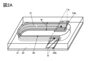
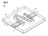
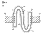
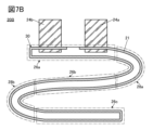
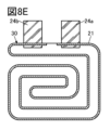
- the first opening has a plurality of extension portions and at least one bent portion
- the extension portions have a shape that is extended in one direction when viewed from above, and one of the extension portions is connected to another of the extension portions via a bent portion.
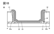
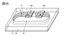
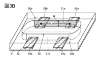
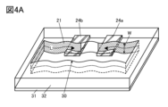
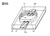
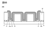
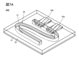
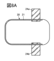
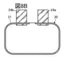
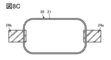
- the channel length L of the transistor 20 corresponds to the distance between the source electrode 24a and the drain electrode 24b in the circumferential direction of the semiconductor layer 21 provided on the sidewall of the opening 30.
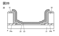
- the channel width W of the transistor 20 is the width of the semiconductor layer 21 along the depth direction of the opening 30. Therefore, since the channel width W can be controlled by the thickness of the insulating layer 32 and the depth of the opening 30, a transistor with an extremely short channel width can be realized. For example, it is possible to realize a transistor with an extremely small channel width that could not be realized with a mass-production exposure tool. Also, it is possible to realize a transistor with a channel width of less than 10 nm without using the extremely expensive exposure tool used in cutting-edge LSI technology.
- a folded structure By connecting two extensions with one bend, a folded structure can be formed in the opening 30.
- the length of the opening 30 can be made significantly greater than the distance between the source electrode 24a and the drain electrode 24b.
- the channel length L can be increased without increasing the area occupied by the transistor.
- a transistor with high saturation properties can be obtained.
- a transistor with an extremely small ratio of the channel width W to the channel length L (W/L ratio) can be realized.
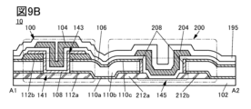
- the insulating layer 106 has a shape that follows the shapes of the upper surface and side surfaces of the semiconductor layer 208, the upper surface and side surfaces near the side ends of the conductive layer 212a, the upper surface and side surfaces near the side ends of the conductive layer 212b, the side surfaces of the insulating layer 110, and the upper surface of the substrate 102.
- the channel length of the transistor 100 can be controlled by the thickness of the insulating layer 110 (specifically, the insulating layer 110b) provided between the conductive layer 112a and the conductive layer 112b. Therefore, a transistor having a channel length shorter than the limit resolution of an exposure device used to manufacture the transistor can be manufactured with high precision.
- the characteristic variation between multiple transistors 100 is also reduced. This makes it possible to stabilize the operation of a semiconductor device including the transistor 100 and to increase its reliability.
- the reduced characteristic variation increases the degree of freedom in circuit design and allows the operating voltage of the semiconductor device to be reduced. This allows the power consumption of the semiconductor device to be reduced.
- the semiconductor layer 108 and the semiconductor layer 208 can each be made of silicon.
- silicon examples include single crystal silicon, polycrystalline silicon, microcrystalline silicon, and amorphous silicon.
- polycrystalline silicon examples include low temperature polysilicon (LTPS).
- Transistors using amorphous silicon in the channel formation region can be formed on a large glass substrate and can be manufactured at low cost. Transistors using polycrystalline silicon in the channel formation region have high field effect mobility and can operate at high speed. Furthermore, transistors using microcrystalline silicon in the channel formation region have higher field effect mobility and can operate at high speed than transistors using amorphous silicon.
- an oxynitride refers to a material whose composition contains more oxygen than nitrogen.
- a nitride oxide refers to a material whose composition contains more nitrogen than oxygen.
- silicon oxynitride refers to a material whose composition contains more oxygen than nitrogen.
- Silicon nitride oxide refers to a material whose composition contains more nitrogen than oxygen.
- the insulating layer 110b is preferably formed by a deposition method such as a sputtering method or a plasma enhanced chemical vapor deposition (PECVD) method.
- a deposition method such as a sputtering method or a plasma enhanced chemical vapor deposition (PECVD) method.
- PECVD plasma enhanced chemical vapor deposition
- the insulating layer 110b it is preferable that substances (e.g., atoms, molecules, and ions) diffuse easily. It can also be said that it is preferable that the diffusion coefficient of the substance in the insulating layer 110b is large. In particular, it is preferable that oxygen diffuses easily in the insulating layer 110b. In other words, it is preferable that the diffusion coefficient of oxygen in the insulating layer 110b is large.
- the oxygen contained in the insulating layer 110b diffuses through the insulating layer 110b and is supplied to the semiconductor layer 108 via the interface between the insulating layer 110b and the semiconductor layer 108, and is also supplied to the semiconductor layer 208 via the interface between the insulating layer 110b and the semiconductor layer 208.
- V O oxygen vacancies
- V O H increases due to an increase in oxygen vacancies (V O ) in the channel formation region, which may shift the threshold voltage of the transistor and increase the drain current (hereinafter also referred to as cutoff current) that flows when the gate voltage is 0 V.
- cutoff current may increase due to a shift in the threshold voltage to the negative side.
- oxygen is supplied to at least the region of the semiconductor layer 108 that is in contact with the insulating layer 110b and the region of the semiconductor layer 208 that is in contact with the insulating layer 110b, that is, the channel formation regions of the transistors 100 and 200, and the oxygen vacancies (V O ) and V O H in the channel formation regions can be reduced.
- V O oxygen vacancies
- V O H oxygen vacancies
- the region of the semiconductor layer 108 in contact with the conductive layer 112a functions as one of the source and drain regions of the transistor 100, and the region in contact with the conductive layer 112b functions as the other.
- the source and drain regions are regions with lower electrical resistance than the channel formation region.
- the source and drain regions can also be said to be regions with a higher carrier concentration and a higher oxygen defect density than the channel formation region.
- the insulating layer 110a is provided between the insulating layer 110b and the conductive layer 112a.
- the insulating layer 110c is provided between the insulating layer 110b and the conductive layer 112b. It is preferable that the insulating layer 110a and the insulating layer 110c each release a small amount of impurities (e.g., hydrogen and water) and are difficult for impurities to permeate. This can prevent the impurities contained in the insulating layer 110a and the insulating layer 110c from diffusing into the channel formation region. Therefore, a transistor that exhibits good electrical characteristics and is highly reliable can be obtained.
- impurities e.g., hydrogen and water
- oxygen can be effectively supplied from the insulating layer 110b to the channel formation region.
- a configuration in which one or both of the insulating layers 110a and 110c are not provided may also be used.
- the insulating layer 110a and the insulating layer 110c each preferably contain nitrogen, and preferably use one or more of the above-mentioned nitrides and nitride oxides.
- silicon nitride or silicon nitride oxide may be preferably used for the insulating layer 110a and the insulating layer 110c.
- one or both of the insulating layer 110a and the insulating layer 110c may use one or more of an oxide and an oxynitride.
- aluminum oxide may be preferably used for the insulating layer 110a and the insulating layer 110c.
- the insulating layer 110a may use the same material as the insulating layer 110c, or a different material.
- different materials refer to materials in which some or all of the constituent elements are different, or materials in which the constituent elements are the same but the composition is different.
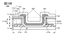
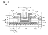
- the thickness T110a of the insulating layer 110a can be, for example, 3 nm or more, 5 nm or more, 10 nm or more, 20 nm or more, 50 nm or more, or 70 nm or more, and can be less than 1 ⁇ m, 500 nm or less, 400 nm or less, 300 nm or less, 200 nm or less, 150 nm or less, or 120 nm or less. As shown in FIG. 11B, the thickness T110a can be the shortest distance between the surface on which the insulating layer 110a is formed (here, the upper surface of the conductive layer 112a) and the lower surface of the insulating layer 110b in a cross-sectional view.
- the thickness T110a of the insulating layer 110a When the thickness T110a of the insulating layer 110a is large, the amount of impurities released from the insulating layer 110a increases, and the amount of impurities diffusing into the channel formation region may increase. On the other hand, when the thickness T110a is small, oxygen contained in the insulating layer 110b may diffuse to the conductive layer 112a side through the insulating layer 110a, and the amount of oxygen supplied to the channel formation region may decrease. By setting the thickness T110a within the above range, oxygen vacancies (V O ) and V O H in the channel formation region can be reduced. In addition, the conductive layer 112a is oxidized by the oxygen contained in the insulating layer 110b, and the electrical resistance of the conductive layer 112a can be prevented from increasing.
- the thickness T110c of the insulating layer 110c can be, for example, 3 nm or more, 5 nm or more, 10 nm or more, 15 nm or more, or 20 nm or more, and can be 1 ⁇ m or less, 500 nm or less, 300 nm or less, 200 nm or less, 150 nm or less, 120 nm or less, or 100 nm or less. As shown in FIG. 11B, the thickness T110c can be the shortest distance between the surface on which the insulating layer 110c is formed (here, the upper surface of the insulating layer 110b) and the lower surface of the conductive layer 112b in a cross-sectional view.
- the thickness T110c of the insulating layer 110c When the thickness T110c of the insulating layer 110c is large, the amount of impurities released from the insulating layer 110c increases, and the amount of impurities diffusing into the channel formation region may increase. On the other hand, when the thickness T110c is small, oxygen contained in the insulating layer 110b may diffuse to the conductive layer 112b side through the insulating layer 110c, and the amount of oxygen supplied to the channel formation region may decrease. By setting the thickness T110c within the above range, oxygen vacancies (V O ) and V O H in the channel formation region can be reduced. In addition, the conductive layer 112b is oxidized by the oxygen contained in the insulating layer 110b, and the electrical resistance of the conductive layer 112b can be prevented from increasing.
- At least one of the region of the semiconductor layer 108 in contact with the insulating layer 110a and the region of the semiconductor layer 108 in contact with the insulating layer 110c may be a region having a lower electrical resistance than the channel formation region (hereinafter, also referred to as a low-resistance region).
- the region may be a region having a higher carrier concentration or a higher oxygen defect density than the channel formation region.
- the semiconductor layer 108 can be configured to have a low-resistance region between the region of the semiconductor layer 108 in contact with the conductive layer 112a (one of the source region and the drain region) and the channel formation region. Similarly, by using a material that releases impurities in the insulating layer 110c, the region of the semiconductor layer 108 in contact with the insulating layer 110c can be a low-resistance region.
- the semiconductor layer 108 can be configured to have a low-resistance region between the region of the semiconductor layer 108 in contact with the conductive layer 112b (the other of the source region and the drain region) and the channel formation region.
- the low resistance regions can function as buffer regions to reduce the drain electric field. These low resistance regions may also function as source or drain regions.
- the conductive layer 112a functions as a drain electrode and the conductive layer 112b functions as a source electrode, by making the region of the semiconductor layer 108 in contact with the insulating layer 110a into a low resistance region, a high electric field is unlikely to occur near the drain region, the generation of hot carriers is suppressed, and deterioration of the transistor can be suppressed.
- the conductive layer 112a functions as a source electrode and the conductive layer 112b functions as a drain electrode, by making the region of the semiconductor layer 108 in contact with the insulating layer 110c into a low resistance region, a high electric field is unlikely to occur near the drain region, the generation of hot carriers is suppressed, and deterioration of the transistor can be suppressed.
- the region of the semiconductor layer 208 in contact with the insulating layer 110a may be a low resistance region compared to the channel formation region.
- This region can also be said to be a region with a high carrier concentration or a high oxygen defect density compared to the channel formation region.
- the region in contact with the insulating layer 110a can be a low resistance region.
- the semiconductor layer 208 can be configured to have a low resistance region between the region in contact with the conductive layer 212a (one of the source region and the drain region) and the channel formation region.
- the low resistance region can function as a buffer region for relaxing the drain electric field. Note that the low resistance region may function as a source region or a drain region.
- the shape of the top surface of the opening 145 is a rectangle with rounded corners, but the present invention is not limited to this, and various shapes can be used as described above.
- the shape of the top surface of the opening 145 can be a circle.
- the top surface shape of opening 145 refers to the shape of the top surface end portion of insulating layer 110 on the opening 145 side.
- the top surface shape of opening 141 refers to the shape of the top surface end portion of insulating layer 110 on the opening 141 side.
- the top surface shape of opening 143 refers to the shape of the bottom surface end portion of conductive layer 112b on the opening 143 side.
- the top surface shapes of openings 141 and 143 can be made to match or roughly match each other.
- the bottom surface end of conductive layer 112b on the opening 143 side match or roughly match the top surface end of insulating layer 110 on the opening 141 side.
- the bottom surface of conductive layer 112b refers to the surface on the insulating layer 110 side.
- the top surface of insulating layer 110 refers to the surface on the conductive layer 112b side.
- openings 141 and 143 do not have to be the same. Furthermore, when the top surface shapes of openings 141 and 143 are circular, openings 141 and 143 may or may not be concentric.
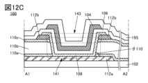
- the channel length L100 of the transistor 100 is indicated by a double-headed dashed arrow.
- the channel length L100 of the transistor 100 corresponds to the length of the side of the insulating layer 110b on the opening 141 side in a cross-sectional view.
- the channel length L100 is determined by the thickness T110b of the insulating layer 110b and the angle ⁇ 110 between the side of the insulating layer 110b on the opening 141 side and the surface on which the insulating layer 110b is to be formed (here, the upper surface of the insulating layer 110a). Therefore, the channel length L100 can be set to a value smaller than the limit resolution of the exposure device, and a transistor of a fine size can be realized.
- a transistor with an extremely small channel length that could not be realized with a conventional exposure device for mass production of flat panel displays (for example, a minimum line width of about 2 ⁇ m or 1.5 ⁇ m).
- a transistor with a channel length of less than 10 nm without using an extremely expensive exposure device used in cutting-edge LSI technology.
- the channel length L100 can be, for example, 5 nm or more, 7 nm or more, or 10 nm or more, and less than 3 ⁇ m, 2.5 ⁇ m or less, 2 ⁇ m or less, 1.5 ⁇ m or less, 1.2 ⁇ m or less, 1 ⁇ m or less, 500 nm or less, 300 nm or less, 200 nm or less, 100 nm or less, 50 nm or less, 30 nm or less, or 20 nm or less.
- the channel length L100 can be 100 nm or more and 1 ⁇ m or less.
- the on-state current of the transistor 100 can be increased.
- the transistor 100 By using the transistor 100, a circuit capable of high-speed operation can be manufactured. Furthermore, the area occupied by the circuit can be reduced. Therefore, a small-sized semiconductor device can be obtained. For example, when the semiconductor device of one embodiment of the present invention is applied to a large display device or a high-definition display device, even if the number of wirings is increased, signal delay in each wiring can be reduced and display unevenness can be suppressed. Furthermore, since the area occupied by the circuit can be reduced, the frame of the display device can be narrowed.
- the shape of the side of the insulating layer 110 on the opening 141 side is shown as straight lines in a cross-sectional view, but this is not a limitation of one embodiment of the present invention.
- the shape of the side of the insulating layer 110 on the opening 141 side may be curved, and the side may have both straight and curved regions.
- the width D141 of opening 141 is indicated by a double-headed arrow with a two-dot chain line.
- Figure 11A shows an example in which the top surface shape of opening 141 is circular.
- width D141 corresponds to the diameter of the circle
- channel width W100 of transistor 100 is the length of the circumference of the circle.
- channel width W100 is ⁇ x D141. In this way, when the top surface shape of opening 141 is circular, a transistor with a smaller channel width W100 can be realized compared to other shapes.
- the width D141 of the opening 141 may vary in the depth direction.
- the average value of the diameter at the highest point of the insulating layer 110b (or insulating layer 110) in a cross-sectional view, the diameter at the lowest point, and the diameter at the midpoint between these three diameters may be used as the width D141 of the opening 141.
- the diameter of the opening 141 may be any one of the diameters at the highest point of the insulating layer 110b (or insulating layer 110) in a cross-sectional view, the diameter at the lowest point, and the diameter at the midpoint between these two diameters.
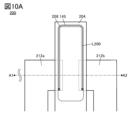
- the channel length L200 of the transistor 200 is indicated by a solid double-headed arrow.
- the channel length L200 corresponds to the distance between the conductive layer 212a and the conductive layer 212b along the circumferential direction of the semiconductor layer 208 provided on the sidewall of the opening 145.
- the channel length L200 of the transistor 200 can be controlled by the top surface shape and size of the opening 145. Therefore, the channel length L200 can be made larger than the channel length L100.
- the channel width W200 can be, for example, 5 nm or more, 7 nm or more, or 10 nm or more, and can be less than 3 ⁇ m, 2.5 ⁇ m or less, 2 ⁇ m or less, 1.5 ⁇ m or less, 1.2 ⁇ m or less, 1 ⁇ m or less, 500 nm or less, 300 nm or less, 200 nm or less, 100 nm or less, 50 nm or less, 30 nm or less, or 20 nm or less.
- the channel length L100 of the transistor 100 can be set to a value smaller than the limit resolution of the exposure device.
- the channel length L100 is determined by the film thickness of the insulating layer 110b, when multiple transistors 100 are formed on the same surface in the same process, all the transistors 100 have the same channel length.
- the channel length L200 of the transistor 200 can be controlled by the upper surface shape and size of the opening 145.
- the transistor 200 can be formed by sharing some of the processes with the transistor 100. Therefore, the transistor 100 with a short channel length and the transistor 200 with a longer channel length can be formed on the same surface with good productivity.
- n oxide also written as AZO
- indium aluminum zinc oxide In-Al-Zn oxide, also written as IAZO
- indium tin zinc oxide In-Sn-Zn oxide, also written as ITZO (registered trademark)
- indium titanium zinc oxide In-Ti-Zn oxide
- indium gallium zinc oxide In-Ga-Zn oxide, also written as IGZO
- indium gallium tin zinc oxide In-Ga-Sn-Zn oxide, also written as IGZTO
- indium gallium aluminum zinc oxide In-Ga-Al-Zn oxide, also written as IGAZO, IGZAO, or IAGZO
- indium tin oxide containing silicon also written as ITSO
- gallium tin oxide Ga-Sn oxide
- aluminum tin oxide Al-Sn oxide
- materials that do not contain Zn such as indium oxide, are suitable because they have high affinity with Si processes.
- materials containing Zn are suitable because they can improve crystallinity.
- the field effect mobility of the transistor can be increased.
- a transistor with a large on-current can be realized.
- the metal oxide may contain one or more nonmetallic elements.
- the carrier concentration increases or the band gap decreases, which may increase the field effect mobility of the transistor.
- nonmetallic elements include carbon, nitrogen, phosphorus, sulfur, selenium, fluorine, chlorine, bromine, and hydrogen.
- the metal oxide becomes highly crystalline and the diffusion of impurities in the metal oxide can be suppressed. This suppresses fluctuations in the electrical characteristics of the transistor and increases its reliability.
- the electrical characteristics and reliability of the transistors vary depending on the composition of the metal oxide applied to the semiconductor layer 108 and the semiconductor layer 208. Therefore, by varying the composition of the metal oxide depending on the electrical characteristics and reliability required of the transistor, a semiconductor device that combines excellent electrical characteristics and high reliability can be obtained.
- the atomic ratio of In in the In-M-Zn oxide may be less than the atomic ratio of element M.
- the conductive layer 112a, the conductive layer 112b, the conductive layer 104, the conductive layer 204, the conductive layer 212a, conductive layer 212b may each have a single layer structure or a laminated structure of two or more layers.
- the conductive layers 112a, 112b, 104, 204, 212a, and 212b may each be a Cu-X alloy film (X is Mn, Ni, Cr, Fe, Co, Mo, Ta, or Ti).
- X is Mn, Ni, Cr, Fe, Co, Mo, Ta, or Ti.
- the insulating layer 106 has a single-layer structure, it is preferable to use an oxide or an oxynitride for the insulating layer 106. Specifically, silicon oxide or silicon oxynitride can be suitably used for the insulating layer 106.
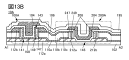
- the semiconductor device 10A has a transistor 100A, a transistor 200A, and an insulating layer 110.
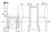
- the transistor 100A differs from the transistor 100 shown in FIG. 9A etc. mainly in that the transistor 100A has insulating layers 147 and 149 and that the semiconductor layer 108 does not contact the side surface of the conductive layer 112b.
- the transistor 200A differs from the transistor 200 shown in FIG. 9A etc. mainly in that the transistor 200A has insulating layers 247 and 249.
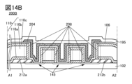
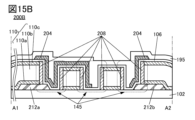
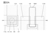
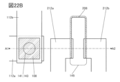
- Extending portion 146a, extending portion 146b, and extending portion 146c have a shape that extends in one direction (in FIG. 14A, a direction perpendicular to dashed line A1-A2) when viewed from above.
- bending portion 148a and bending portion 148b are provided such that one end is bent relative to the other end when viewed from above.
- a folded structure can be formed in the opening 145.
- the length of the opening 145 can be significantly longer than the distance between the conductive layers 212a and 212b. This significantly increases the channel length of the transistor 200B, and increases the saturation of the transistor 200B.
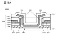
- the insulating layer 110 includes an insulating layer 110a on the conductive layer 212a and the conductive layer 212b, an insulating layer 110b1 on the insulating layer 110a, an insulating layer 110d1 on the insulating layer 110b1, an insulating layer 110d2 on the insulating layer 110d1 and the conductive layer 216, an insulating layer 110b2 on the insulating layer 110d2, and an insulating layer 110c on the insulating layer 110b2.
- the conductive layer 216 functions as a back gate electrode (which can also be called a second gate electrode) of the transistor 200C.
- the conductive layer 216 is preferably located on the insulating layer 110d1.
- the conductive layers 212a and 212b and the conductive layer 216 are electrically insulated from each other by the insulating layers 110a, 110b1, and 110d1.
- the conductive layer 216 preferably has an opening, and an opening 145 is preferably provided inside the opening.
- the conductive layer 216 may be electrically connected to the conductive layer 212a or the conductive layer 212b.
- the conductive layer 212a and the conductive layer 216 may be in contact with each other through an opening provided in the insulating layers 110a, 110b1, and 110d1.
- the conductive layer 216 may have a single layer structure or a stacked structure of two or more layers.
- the conductive layer 216 may be made of any of the materials that can be used for the conductive layer 212a, the conductive layer 212b, and the conductive layer 204.
- FIG. 16A illustrates an example in which the cross-sectional shape of the conductive layer 216 has a tapered shape
- the conductive layer 216 may be arranged so that its cross-sectional shape is vertical. With this arrangement, the side surface of the conductive layer 216 and the surface of the semiconductor layer 208 that contacts the insulating layer 110 become parallel. With this arrangement, the potential given to the conductive layer 216 can be efficiently applied to the semiconductor layer 208, which is preferable.
- the insulating layer 110d2 covers the upper and side surfaces of the conductive layer 216.
- the insulating layer 110d2 is provided so as to cover a portion of the opening of the conductive layer 216. It is preferable that the insulating layer 110d2 contacts the insulating layer 110d1 through the opening.
- the insulating layer 110d1 and the insulating layer 110d2 have the same configuration as the insulating layers 110a and 110c. Specifically, it is preferable that the insulating layer 110d1 and the insulating layer 110d2 are made of a film into which oxygen does not easily diffuse. It is also preferable that the insulating layer 110d1 and the insulating layer 110d2 are made of a film into which hydrogen does not easily diffuse. By providing such insulating layer 110d1 and insulating layer 110d2, it is possible to prevent the conductive layer 216 from being oxidized. It is also possible to prevent the hydrogen contained in the conductive layer 216 from diffusing into the semiconductor layer 208.
- FIG. 16A shows an example in which the thickness of insulating layer 110d1 is uniform regardless of location, the present invention is not limited to this.
- insulating layer 110d1 may have different thicknesses in areas that overlap with conductive layer 216 and areas that do not overlap. For example, when processing the film that will become conductive layer 216, parts of insulating layer 110d1 that do not overlap with conductive layer 216 may be removed, resulting in a thinner thickness.
- the insulating layer 110b2 preferably covers the upper and side surfaces of the conductive layer 216 via the insulating layer 110d2.
- the insulating layer 110b2 is preferably provided so as to cover a portion of the opening of the conductive layer 216 via the insulating layer 110d2.
- the insulating layer 110b1 and the insulating layer 110b2 can each have a configuration similar to that applicable to the insulating layer 110b. Specifically, it is preferable to use a layer containing oxygen for each of the insulating layers 110b1 and 110b2, and it is preferable to have a region with a higher oxygen content than at least one of the insulating layers 110a, 110c, 110d1, and 110d2.
- the structure of the insulating layer 110 can be made symmetrical above and below the conductive layer 216.
- oxygen can be supplied to the semiconductor layer 208 from both the insulating layers 110b1 and 110b2, improving the characteristics of the transistor.
- the present invention is not limited to the above, and for example, it is also possible to configure the device without providing insulating layer 110b1. It is also possible to configure the device without providing insulating layer 110d1 and insulating layer 110d2.
- the semiconductor layer 208 has an area that overlaps with the conductive layer 204 via the insulating layer 106 and with the conductive layer 216 via a part of the insulating layer 110 (particularly, the insulating layer 110b2 and the insulating layer 110d2).
- a part of the semiconductor layer 208 is sandwiched between the side of the conductive layer 204 and the side of the conductive layer 216, a part of the insulating layer 110 (particularly, the insulating layer 110b2 and the insulating layer 110d2) is provided between at least a part of the semiconductor layer 208 and the side of the conductive layer 204, and the insulating layer 106 is provided between at least a part of the semiconductor layer 208 and the side of the conductive layer 216.
- a part of the insulating layer 110 functions as a backgate insulating layer (which can also be called a second gate insulating layer) of the transistor 200C.
- the transistor 200C has a backgate electrode, the potential of the backgate side (also called the backchannel) of the semiconductor layer 208 can be fixed. Therefore, the saturation of the Id-Vd characteristics of the transistor 200C can be further improved.
- the transistor 200C has a back gate electrode, the potential of the back channel of the semiconductor layer 208 can be fixed, and a negative shift in the threshold voltage can be suppressed. This makes it possible to realize a transistor with normally-off characteristics (i.e., a threshold voltage of a positive value).
- Transistor 200C has a region in which conductive layer 216, insulating layer 110, semiconductor layer 208, insulating layer 106, and conductive layer 204 overlap in this order in one direction without any other layers in between. By widening this region, the electric field of the back channel of semiconductor layer 208 can be more reliably controlled.
- the shortest distance between the conductive layer 216 and the semiconductor layer 208 may differ on the left and right sides of the opening in the insulating layer 110.
- transistor 100 can be configured to have a back gate.
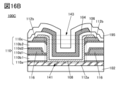
- Transistor 100C shown in FIG. 16B differs from transistor 100 mainly in that it has conductive layer 116 on conductive layer 112a and that insulating layer 110 has a six-layer structure.
- the conductive layer 116 corresponds to the conductive layer 216 described above, and the description of the conductive layer 216 can be referred to. That is, the conductive layer 116 functions as a backgate electrode of the transistor 100C.
- the insulating layer 110 has the same structure as the insulating layer 110 shown in FIG. 16A. That is, a part of the insulating layer 110 functions as a backgate insulating layer of the transistor 100C.
- the semiconductor layer 108 is sandwiched between the side of the conductive layer 104 and the side of the conductive layer 116, a portion of the insulating layer 110 (particularly, the insulating layer 110b2 and the insulating layer 110d2) is provided between at least a portion of the semiconductor layer 108 and the side of the conductive layer 104, and the insulating layer 106 is provided between at least a portion of the semiconductor layer 108 and the side of the conductive layer 116.
- the transistor 100C has a back gate electrode, the potential of the back gate side (also called the back channel) of the semiconductor layer 108 can be fixed. Therefore, the saturation of the Id-Vd characteristics of the transistor 200C can be further improved.
- the transistor 100C has a back gate electrode, the potential of the back channel of the semiconductor layer 108 can be fixed, and a negative shift in the threshold voltage can be suppressed. This makes it possible to realize a transistor with normally-off characteristics (i.e., a threshold voltage of a positive value).
- the thin films (insulating films, semiconductor films, conductive films, etc.) that make up semiconductor devices can be formed using methods such as sputtering, chemical vapor deposition (CVD), vacuum deposition, pulsed laser deposition (PLD), ALD, and molecular beam epitaxy (MBE).
- CVD methods include PECVD and thermal CVD.
- thermal CVD method is metal organic chemical vapor deposition (MOCVD).
- the thin film When processing the thin film that constitutes the semiconductor device, a photolithography method or the like can be used.
- the thin film may be processed using a nanoimprint method, a sandblasting method, a lift-off method, or the like.
- island-shaped thin films may be directly formed using a film formation method that uses a shielding mask such as a metal mask.
- the light used for exposure can be, for example, i-line (wavelength 365 nm), g-line (wavelength 436 nm), h-line (wavelength 405 nm), or a mixture of these.
- ultraviolet light, KrF laser light, ArF laser light, etc. can also be used.
- Exposure can also be performed by immersion exposure technology.
- Extreme ultraviolet (EUV) light or X-rays can also be used as the light used for exposure.
- Electron beams can also be used instead of the light used for exposure. Extreme ultraviolet light, X-rays, or electron beams are preferable because they enable extremely fine processing. When exposure is performed by scanning a beam such as an electron beam, a photomask is not required.
- etching the thin film one or more of the following methods can be used: dry etching, wet etching, and sandblasting.
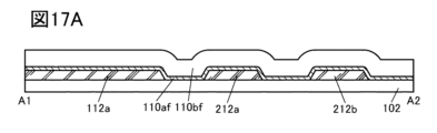
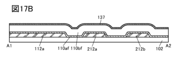
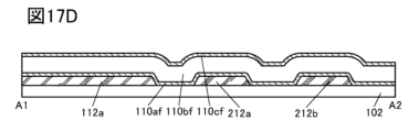
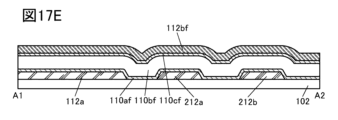
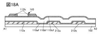
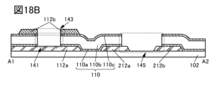
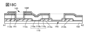
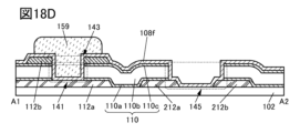
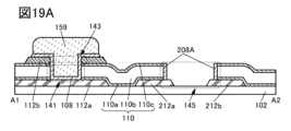
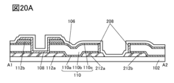
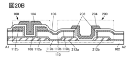
- Fig. 17A to Fig. 20B show cross-sectional views taken along dashed line A1-A2 in Fig. 9A.
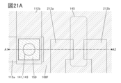
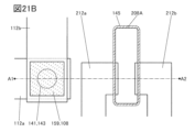
- Fig. 21A to Fig. 22B show top views.
- a film that will become the conductive layer 112a, the conductive layer 212a, and the conductive layer 212b is formed on the substrate 102, and the film is processed to form the conductive layer 112a, the conductive layer 212a, and the conductive layer 212b.
- the film can be preferably formed by a sputtering method.
- the conductive layer 112a, the conductive layer 212a, and the conductive layer 212b can be preferably formed by, for example, a wet etching method. Note that an insulating layer that will become a base film may be stacked on the substrate 102 before the film is formed.
- a conductive film having high conductivity such as copper can be used for the conductive layer 112a, the conductive layer 212a, and the conductive layer 212b.
- a laminated film having a copper layer and an ITSO layer on the copper layer can be used for the conductive layer 112a, the conductive layer 212a, and the conductive layer 212b.
- the conductive layer 112a, the conductive layer 212a, and the conductive layer 212b are disposed on a flat portion on the substrate 102, so that even if a conductive film having high conductivity such as copper is used, the conductive layer 112a, the conductive layer 212a, and the conductive layer 212b can be relatively easily routed. Therefore, the conductive layer 112a, the conductive layer 212a, and the conductive layer 212b can function as wiring with low electrical resistance.
- insulating film 110af which will become insulating layer 110a
- insulating film 110bf which will become insulating layer 110b
- the channel length L100 of transistor 100 and the channel width W200 of transistor 200 depend on the film thickness of insulating film 110bf. Therefore, the film thickness of insulating film 110bf can be set according to the electrical characteristics desired for transistor 100 and transistor 200.
- the substrate temperature during the formation of the insulating film 110af and the insulating film 110bf is preferably 180°C or higher and 450°C or lower, more preferably 200°C or higher and 450°C or lower, even more preferably 250°C or higher and 450°C or lower, even more preferably 300°C or higher and 450°C or lower, even more preferably 300°C or higher and 400°C or lower, even more preferably 350°C or higher and 400°C or lower.
- the substrate temperature during the formation of the insulating film 110af and the insulating film 110bf within the above-mentioned range, it is possible to reduce the release of impurities (e.g., water and hydrogen) from the insulating film 110af and the insulating film 110bf, and to suppress the diffusion of impurities into the semiconductor layer 108. Therefore, it is possible to obtain a transistor that exhibits good electrical characteristics and is highly reliable.
- impurities e.g., water and hydrogen
- oxygen may be supplied to the insulating film 110bf.
- an ion implantation method, an ion doping method, a plasma immersion ion implantation method, or a plasma treatment can be used as a method for supplying oxygen.
- an apparatus that converts oxygen gas into plasma by high-frequency power can be suitably used.
- a PECVD apparatus, a plasma etching apparatus, and a plasma ashing apparatus can be given as an apparatus that converts gas into plasma by high-frequency power.
- the plasma treatment is preferably performed in an atmosphere containing oxygen.
- the plasma treatment is preferably performed in an atmosphere containing one or more of oxygen, nitrous oxide (N 2 O), nitrogen dioxide (NO 2 ), carbon monoxide, and carbon dioxide.
- the conductivity of the metal oxide layer 137 does not matter.
- At least one of an insulating film, a semiconductor film, and a conductive film can be used as the metal oxide layer 137.
- aluminum oxide, hafnium oxide, hafnium aluminate, indium oxide, indium tin oxide (ITO), or indium tin oxide containing silicon (ITSO) can be used as the metal oxide layer 137.
- an atmosphere containing as little hydrogen, water, and the like it is possible to prevent hydrogen, water, and the like from being taken into the insulating film 110af and the insulating film 110bf as much as possible.
- an oven a rapid heating (RTA: Rapid Thermal Annealing) device, and the like can be used. Using an RTA device can shorten the heating process time.
- RTA Rapid Thermal Annealing
- the film 139 is preferably a conductive film or a semiconductor film.
- the film 139 can be a metal oxide film, a metal film, or an alloy film. It is preferable to use a metal oxide as the film 139 and form it by a sputtering method or the like in an atmosphere containing oxygen, because oxygen can be supplied to the insulating film 110bf even during the formation of the film 139.
- the thickness of film 139 is preferably thin. Specifically, the thickness of film 139 is preferably 1 nm or more, 2 nm or more, or 3 nm or more, and 20 nm or less, 15 nm or less, or 10 nm or less. Typically, the thickness can be about 5 nm.
- a wet etching method can be suitably used to remove the film 139.
- a conductive film or a semiconductor film containing one or more of indium, zinc, gallium, tin, aluminum, chromium, tantalum, titanium, molybdenum, nickel, iron, cobalt, and tungsten can be used.
- insulating film 110cf which will become insulating layer 110c, is formed on insulating film 110bf (FIG. 17D).
- the description of the formation of insulating film 110af and insulating film 110bf can be referenced for the formation of insulating film 110cf, so a detailed description will be omitted.
- the ALD method it is preferable to use a film formation method such as thermal ALD or PEALD (Plasma Enhanced ALD).
- a film formation method such as thermal ALD or PEALD (Plasma Enhanced ALD).
- the thermal ALD method is preferable because it shows extremely high coating properties.
- the PEALD method is preferable because it shows high coating properties and allows low-temperature film formation.
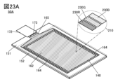
- connection portion 140 is provided on the outside of the display portion 162.
- the connection portion 140 can be provided along one side or multiple sides of the display portion 162. There may be one or multiple connection portions 140.
- FIG. 23A shows an example in which the connection portion 140 is provided so as to surround the four sides of the display portion.
- the connection portion 140 electrically connects the common electrode of the display element and the conductive layer, and can supply a potential to the common electrode.
- liquid crystal elements also called liquid crystal devices
- light-emitting devices Other elements that can be used include shutter-type or optical interference-type MEMS (Micro Electro Mechanical Systems) elements, display elements that use microcapsules, electrophoresis, electrowetting, or electronic liquid powder (registered trademark) methods, etc.
- QLEDs Quantum-dot LEDs that use a light source and color conversion technology using quantum dot materials.
- Liquid crystal materials that can be used in liquid crystal elements include, for example, thermotropic liquid crystal, low molecular weight liquid crystal, polymer liquid crystal, polymer dispersed liquid crystal (PDLC: Polymer Dispersed Liquid Crystal), polymer network liquid crystal (PNLC: Polymer Network Liquid Crystal), ferroelectric liquid crystal, and antiferroelectric liquid crystal.
- thermotropic liquid crystal low molecular weight liquid crystal
- polymer liquid crystal polymer dispersed liquid crystal
- PNLC Polymer Network liquid crystal
- ferroelectric liquid crystal and antiferroelectric liquid crystal.
- these liquid crystal materials can exhibit cholesteric phase, smectic phase, cubic phase, chiral nematic phase, isotropic phase, blue phase, etc.
- either positive type liquid crystal or negative type liquid crystal can be used as the liquid crystal material, and can be selected according to the mode or design to be applied.
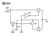
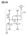
- writing data to the latch circuit LAT such that the signal input from terminal SP2 is output to terminal LIN may be simply referred to as "writing data to the latch circuit LAT.”
- writing data with a value of "1" to the latch circuit LAT may be simply referred to as "writing data to the latch circuit LAT.”
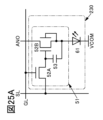
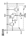
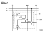
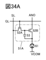
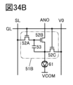
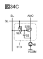
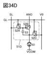
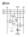
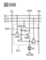
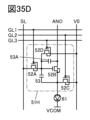
- Transistor 52B has the function of controlling the amount of current flowing through light-emitting device 61.
- Capacitive element 53 has the function of maintaining the gate potential of transistor 52B. The intensity of the light emitted by light-emitting device 61 is controlled according to an image signal supplied to the gate of transistor 52B.
- the above-mentioned semiconductor device can be suitably used in the pixel circuit 51.
- the transistor 52B that functions as a drive transistor that controls the current flowing through the light-emitting device 61 preferably has high saturation.
- the transistor 52B By using one of the transistors 20, 200, and 200A, which have a long channel length, as the transistor 52B, a highly reliable display device can be obtained.
- the transistor 100 as the transistor 52A, the area occupied by the pixel circuit 51A can be reduced, resulting in a high-definition display device.
- One of the source and drain of transistor 52C is electrically connected to one of the source and drain of transistor 52B.
- the other of the source and drain of transistor 52C is electrically connected to wiring V0.
- a reference potential is supplied to wiring V0.
- the gate of transistor 52C is electrically connected to wiring GL.
- An insulating layer 195 is provided to cover the transistor 52A, the transistor 52B, and the capacitor 53, an insulating layer 233 is provided to cover the insulating layer 195, and an insulating layer 235 is provided to cover the insulating layer 233.
- a light-emitting device 61 can be provided on the insulating layer 235.
- FIG. 25C shows a pixel electrode 111 that functions as one electrode of the light-emitting device 61.
- the insulating layer 195, the insulating layer 233, the insulating layer 110a, the insulating layer 110b, and the insulating layer 110c have a first opening that reaches the conductive layer 212b, and a conductive layer 234 is provided to cover the first opening.
- the conductive layer 234 is electrically connected to the conductive layer 212b through the first opening.
- the insulating layer 235 has a second opening that reaches the conductive layer 234, and a pixel electrode 111 is provided to cover the second opening.
- the pixel electrode 111 is electrically connected to the conductive layer 234 through the second opening.
- the insulating layer 195 can be described in the above, and detailed description thereof will be omitted.
- the insulating layer 233 and the insulating layer 235 have the function of reducing unevenness caused by the transistors 52A, 52B, and 52C, and making the surface on which the light-emitting device 61 is formed flatter. Note that in this specification and the like, the insulating layer 233 and the insulating layer 235 may each be referred to as a flattening layer.
- the insulating layer 233 and the insulating layer 235 are preferably organic insulating films.
- Examples of materials that can be used for the organic insulating film include acrylic resin, polyimide resin, epoxy resin, polyamide resin, polyimideamide resin, siloxane resin, benzocyclobutene resin, phenol resin, and precursors of these resins.
- the insulating layer 235 may have a laminated structure of an organic insulating film and an inorganic insulating film. It is preferable that the insulating layer 235 has a laminated structure of an organic insulating film and an inorganic insulating film on the organic insulating film. This allows the inorganic insulating film to function as an etching protection layer when forming the light-emitting device 61.
- the display device 50B has a configuration in which a pixel circuit, a driver circuit, and the like are provided on a substrate 310.
- the display device 50B has an element layer 71, an element layer 73, an element layer 75, and a wiring layer 77.
- the wiring layer 77 is a layer in which wirings are provided.
- Transistor 300 can be a transistor included in element layer 71.
- Transistor MTCK can be a transistor included in element layer 73.
- Light-emitting device 130 can be a light-emitting device included in element layer 75.
- a semiconductor substrate for example, a single crystal substrate made of silicon or germanium
- a semiconductor substrate for example, an SOI (Silicon On Insulator) substrate, a glass substrate, a quartz substrate, a plastic substrate, a sapphire glass substrate, a metal substrate, a stainless steel substrate, a substrate having stainless steel foil, a tungsten substrate, a substrate having tungsten foil, a flexible substrate, a laminated film, paper containing a fibrous material, or a base film
- the substrate 310 is described as a semiconductor substrate having silicon as a material. Therefore, the transistor included in the element layer 71 can be a transistor having silicon (also called a Si transistor).
- the transistor 300 has an element isolation layer 312, a conductive layer 316, an insulating layer 315, an insulating layer 317, a semiconductor region 313 formed of a part of the substrate 310, and a low-resistance region 314a and a low-resistance region 314b that function as a source region or a drain region. Therefore, the transistor 300 is a Si transistor. Note that FIG.
- FIG. 27 shows a configuration in which one of the source and drain of the transistor 300 is electrically connected to a conductive layer 330, a conductive layer 356, and a conductive layer 514, which will be described later, via a conductive layer 328, which will be described later, but the electrical connection configuration of the display device of one embodiment of the present invention is not limited to this.
- the display device of one embodiment of the present invention may have a configuration in which, for example, the gate of the transistor 300 is electrically connected to the conductive layer 514 via the conductive layer 328.
- the transistor 300 can be made into a Fin type by, for example, configuring the upper surface and the side surface in the channel width direction of the semiconductor region 313 to be covered by the conductive layer 316 via the insulating layer 315 that functions as a gate insulating layer.
- the effective channel width can be increased, and the on characteristics of the transistor 300 can be improved.
- the contribution of the electric field of the gate electrode can be increased, and therefore the off characteristics of the transistor 300 can be improved.
- the transistor 300 may be a planar type instead of a Fin type.
- the transistor 300 may be either a p-channel type or an n-channel type. Alternatively, multiple transistors 300 may be provided, and both p-channel and n-channel types may be used.
- the conductive layer 316 which functions as a gate electrode, can be made of a semiconductor material such as silicon containing an element that imparts n-type conductivity, such as arsenic or phosphorus, or an element that imparts p-type conductivity, such as boron or aluminum.
- the conductive layer 316 can be made of a conductive material such as a metal material, an alloy material, or a metal oxide material.
- the work function is determined by the material of the conductor, so the threshold voltage of the transistor can be adjusted by selecting the material of the conductor. Specifically, it is preferable to use one or both of titanium nitride and tantalum nitride as the conductor. Furthermore, in order to achieve both conductivity and embeddability, it is preferable to use one or both of tungsten and aluminum as a laminated material for the conductor, and in particular, it is preferable to use tungsten in terms of heat resistance.
- the element isolation layer 312 is provided to isolate multiple transistors formed on the substrate 310 from each other.
- the element isolation layer can be formed, for example, by using a LOCOS (Local Oxidation of Silicon) method, a STI (Shallow Trench Isolation) method, or a mesa isolation method.
- LOCOS Local Oxidation of Silicon
- STI Shallow Trench Isolation
- an insulating layer 320 and an insulating layer 322 are stacked in this order from the substrate 310 side.
- Insulating layer 320 and insulating layer 322 may be made of, for example, one or more selected from silicon oxide, silicon oxynitride, silicon nitride oxide, silicon nitride, aluminum oxide, aluminum oxynitride, aluminum nitride oxide, and aluminum nitride.
- the insulating layer 322 may function as a planarizing film that flattens steps caused by the insulating layer 320 and the transistor 300 covered by the insulating layer 322.
- the top surface of the insulating layer 322 may be planarized by a planarization process using a chemical mechanical polishing (CMP) method to improve flatness.
- CMP chemical mechanical polishing
- a conductive layer 328 is embedded in the insulating layer 320 and the insulating layer 322, and connects to the transistor MTCK and the like that are provided above the insulating layer 322.
- the conductive layer 328 functions as a plug or wiring.
- the conductive layer 328 can be made of a material that can be used for the conductive layer MPG.
- a wiring layer 77 is provided on the transistor 300.
- the wiring layer 77 includes, for example, an insulating layer 324, an insulating layer 326, a conductive layer 330, an insulating layer 350, an insulating layer 352, an insulating layer 354, and a conductive layer 356.
- Insulating layer 324 and insulating layer 326 are laminated in this order on insulating layer 322 and conductive layer 328.
- an opening is formed in insulating layer 324 and insulating layer 326 in the area overlapping conductive layer 328.
- conductive layer 330 is embedded in the opening.
- Insulating layer 350, insulating layer 352, and insulating layer 354 are laminated in this order on insulating layer 326 and conductive layer 330. In addition, in the region overlapping conductive layer 330, openings are formed in insulating layer 350, insulating layer 352, and insulating layer 354. Conductive layer 356 is embedded in the opening.
- the insulating layers 324 and 350 use an insulator having a barrier property against one or more selected from hydrogen, oxygen, and water, similar to the insulating layer 592. It is also preferable that the insulating layers 326, 352, and 354 use an insulator having a relatively low dielectric constant, similar to the insulating layer 594, in order to reduce the parasitic capacitance generated between wirings.
- the insulating layers 326, 352, and 354 function as an interlayer insulating film and a planarizing film. It is also preferable that the conductive layers 330 and 356 include a conductor having a barrier property against one or more selected from hydrogen, oxygen, and water.
- An insulating layer 512 is provided above the insulating layer 354 and the conductive layer 356.
- An insulating layer IS1 is provided on the insulating layer 512.
- a conductive layer 514 that functions as a plug or wiring is embedded in the insulating layer IS1 and the insulating layer 512. This electrically connects one of the source and drain of the transistor MTCK to one of the source and drain of the transistor 300.
- a material that can be used for the conductive layer MPG can be used for the conductive layer 514.
- the transistor MTCK is provided on the insulating layer IS1 and the conductive layer 514.
- An insulating layer IS3 is formed above the transistor MTCK.
- An insulating layer IS2 is formed below the insulating layer IS3.
- An insulating layer 574 and an insulating layer 581 are laminated in this order on the insulating layer IS3.
- a conductive layer MPG that functions as a plug or wiring is embedded in the insulating layer GI1, the insulating layer IS2, the insulating layer IS3, the insulating layer 574, and the insulating layer 581. Note that the insulating layers, conductive layers, and semiconductor layers around the transistor MTCK refer to the second embodiment.
- the insulating layer 574 preferably has a function of suppressing the diffusion of impurities such as water and hydrogen (e.g., hydrogen atoms and/or hydrogen molecules).
- the insulating layer 574 preferably functions as a barrier insulating film that suppresses the impurities from being mixed into the transistor MTCK.
- the insulating layer 574 also preferably has a function of suppressing the diffusion of oxygen (e.g., oxygen atoms and/or oxygen molecules).
- the insulating layer 574 preferably has lower oxygen permeability than the insulating layer IS2 and the insulating layer IS3.
- the insulating layer 574 preferably functions as a barrier insulating film that suppresses the diffusion of impurities such as water and hydrogen. Therefore, the insulating layer 574 is preferably made of an insulating material that has a function of suppressing the diffusion of impurities such as hydrogen atoms, hydrogen molecules, water molecules, nitrogen atoms, nitrogen molecules, nitrogen oxide molecules (e.g., N2O , NO, and NO2 ), and copper atoms (through which the above impurities are unlikely to permeate). Alternatively, it is preferable to use an insulating material that has a function of suppressing the diffusion of oxygen (e.g., oxygen atoms and/or oxygen molecules) (through which the above oxygen is unlikely to permeate).
- oxygen e.g., oxygen atoms and/or oxygen molecules
- an insulator having a function of suppressing the permeation of impurities such as water and hydrogen and oxygen for example, an insulator containing one or more selected from boron, carbon, nitrogen, oxygen, fluorine, magnesium, aluminum, silicon, phosphorus, chlorine, argon, gallium, germanium, yttrium, zirconium, lanthanum, neodymium, hafnium, and tantalum may be used in a single layer or in a laminated form.
- an insulator having a function of suppressing the permeation of impurities such as water and hydrogen and oxygen for example, metal oxides such as aluminum oxide, magnesium oxide, gallium oxide, germanium oxide, yttrium oxide, zirconium oxide, lanthanum oxide, neodymium oxide, hafnium oxide, and tantalum oxide can be mentioned.
- an oxide containing aluminum and hafnium (hafnium aluminate) can be mentioned as an oxide containing aluminum and hafnium (hafnium aluminate).
- the insulating layer 574 it is preferable to use aluminum oxide or silicon nitride for the insulating layer 574. This can prevent impurities such as water and hydrogen from diffusing from above the insulating layer 574 to the transistor MTCK. Alternatively, it can prevent oxygen contained in the insulating layer IS3, etc. from diffusing above the insulating layer 574.
- Insulating layer 592 and insulating layer 594 are laminated in this order on insulating layer 574 and insulating layer 581.
- an insulating film (referred to as a barrier insulating film) having a barrier property that prevents impurities such as water and hydrogen from diffusing from the substrate 310 and the transistor MTCK to a region above the insulating layer 592 (for example, a region where the light-emitting device 130R, the light-emitting device 130G, and the light-emitting device 130B are provided). Therefore, it is preferable to use an insulating material for the insulating layer 592 that has a function of suppressing the diffusion of impurities such as hydrogen atoms, hydrogen molecules, and water molecules (the impurities are unlikely to permeate through the insulating material).
- an insulating material for the insulating layer 592 that has a function of suppressing the diffusion of impurities such as nitrogen atoms, nitrogen molecules, nitrogen oxide molecules (for example, N 2 O, NO, and NO 2 ), and copper atoms (the oxygen is unlikely to permeate through the insulating material).
- impurities such as nitrogen atoms, nitrogen molecules, nitrogen oxide molecules (for example, N 2 O, NO, and NO 2 ), and copper atoms (the oxygen is unlikely to permeate through the insulating material).
- it is preferable to have a function of suppressing the diffusion of oxygen for example, one or both of oxygen atoms and oxygen molecules).
- silicon nitride formed by the CVD method can be used as a film with barrier properties against hydrogen.
- insulating layer 594 is preferably an interlayer film with a low dielectric constant. For this reason, materials that can be used for insulating layer 581 can be used for insulating layer 594.
- a conductive layer MPG functioning as a plug or wiring is embedded in insulating layers GI1, IS2, IS3, 574, and 581, and a conductive layer 596 functioning as a plug or wiring is embedded in insulating layers 592 and 594.
- conductive layer MPG and conductive layer 596 are electrically connected to a light-emitting device or the like provided above insulating layer 594.
- a conductive layer that functions as a plug or wiring may be given the same reference symbol as a group of multiple structures.
- the wiring and the plug that connects to the wiring may be an integrated unit. That is, there are cases where a part of the conductive layer functions as the wiring, and cases where a part of the conductive layer functions as the plug.
- each plug and wiring e.g., conductive layer MPG and conductive layer 596
- one or more conductive materials selected from metal materials, alloy materials, metal nitride materials, and metal oxide materials can be used in a single layer or in a laminated form. It is preferable to use a high melting point material such as tungsten or molybdenum that has both heat resistance and conductivity, and tungsten is preferably used. Alternatively, it is preferable to form the wiring from a low resistance conductive material such as aluminum or copper. By using a low resistance conductive material, the wiring resistance can be reduced.
- Insulating layer 598 and insulating layer 599 are formed in order on insulating layer 594 and conductive layer 596.
- insulating layer 598 is preferably made of an insulator having barrier properties against one or more of hydrogen, oxygen, and water.
- insulating layer 599 is preferably made of an insulator having a relatively low dielectric constant in order to reduce parasitic capacitance between wirings. Insulating layer 599 also functions as an interlayer insulating film and a planarizing film.
- the light-emitting device 130 and the connection portion 140 are formed on the insulating layer 599.
- connection portion 140 may be called a cathode contact portion, and is electrically connected to the cathode electrodes of the light-emitting devices 130R, 130G, and 130B.
- the connection portion 140 has one or more conductive layers selected from conductive layers 182a to 182c described below, at least one conductive layer from conductive layers 126a to 126c described below, one or more conductive layers selected from conductive layers 129a to 129c described below, a common layer 114 described below, and a common electrode 115 described below.
- connection portion 140 may be provided so as to surround the four sides of the display portion in a plan view, or may be provided within the display portion (e.g., between adjacent light-emitting devices 130) (not shown).
- Light-emitting device 130R has conductive layer 182a, conductive layer 126a on conductive layer 182a, and conductive layer 129a on conductive layer 126a. All of conductive layer 182a, conductive layer 126a, and conductive layer 129a can be called pixel electrodes, or some of them can be called pixel electrodes.
- Light-emitting device 130G has conductive layer 182b, conductive layer 126b on conductive layer 182b, and conductive layer 129b on conductive layer 126b. As with light-emitting device 130R, all of conductive layer 182b, conductive layer 126b, and conductive layer 129b can be called pixel electrodes, or some of them can be called pixel electrodes.
- Light-emitting device 130B has conductive layer 182c, conductive layer 126c on conductive layer 182c, and conductive layer 129c on conductive layer 126c.
- conductive layer 182c, conductive layer 126c, and conductive layer 129c can all be referred to as pixel electrodes, or only some of them can be referred to as pixel electrodes.
- the conductive layers 182a to 182c and the conductive layers 126a to 126c may be, for example, conductive layers that function as reflective electrodes.
- conductive layers that function as reflective electrodes for example, silver, aluminum, or an alloy film of silver (Ag), palladium (Pd), and copper (Cu) (Ag-Pd-Cu (APC) film) may be used as a conductive layer with high reflectivity to visible light.
- the conductive layers 182a to 182c and the conductive layers 126a to 126c may be, for example, a stacked film of aluminum sandwiched between a pair of titanium layers (a stacked film of Ti, Al, and Ti in this order), or a stacked film of silver sandwiched between a pair of indium tin oxide layers (a stacked film of ITO, Ag, and ITO in this order).
- a conductive layer that functions as a reflective electrode may be used for the conductive layers 182a to 182c, and a material with high light-transmitting properties may be used for the conductive layers 126a to 126c.
- materials with high light-transmitting properties include an alloy of silver and magnesium and indium tin oxide (sometimes referred to as ITO).
- a conductive material that is light-transmitting and light-reflective for the conductive layers 129a to 129c which are the upper electrodes (common electrodes)
- a conductive material that is light-reflective for the conductive layers 182a to 182c which are the lower electrodes (pixel electrodes)
- the conductive layers 126a to 126c it is preferable to use a conductive material that is light-transmitting and light-reflective for the conductive layers 129a to 129c, which are the upper electrodes (common electrodes), and to use a conductive material that is light-reflective for the conductive layers 182a to 182c, which are the lower electrodes (pixel electrodes), and the conductive layers 126a to 126c.
- an insulating layer containing an organic material can be suitably used.
- acrylic resin, polyimide resin, epoxy resin, polyamide resin, polyimideamide resin, siloxane resin, benzocyclobutene resin, phenolic resin, or precursors of these resins can be applied to layer 128.
- a photosensitive resin can be used for layer 128. Examples of photosensitive resins include positive-type materials and negative-type materials.
- the taper angle ⁇ 1 of the insulating layer 127 is less than 90°, preferably 60° or less, and more preferably 45° or less.
- Display device 50B is a top emission type. Light emitted by the light emitting device is emitted towards substrate 119. For this reason, it is preferable to use a material that is highly transparent to visible light for substrate 119. For example, a substrate that is highly transparent to visible light may be selected for substrate 119 from among the substrates that can be used for substrate 310.
- the pixel electrode contains a material that reflects visible light
- the opposing electrode (common electrode 115) contains a material that transmits visible light.
- the gaze detection unit 84 has a function of acquiring information about the user's gaze. Specifically, it has a function of detecting the user's gaze.
- the user's gaze may be acquired, for example, by an eye tracking method such as the Pupil Center Corneal Reflection method or the Bright/Dark Pupil Effect method. Alternatively, it may be acquired by an eye tracking method using a laser or ultrasound.
- the sensor 97 may be used to measure the surrounding temperature, humidity, illuminance, odor, etc.
- the sensor 97 may also be used to obtain information for personal authentication using, for example, a fingerprint, palm print, iris, retina, pulse shape (including vein shape and artery shape), or face.
- the sensor 97 may also be used to measure the number of times the user blinks, eyelid behavior, pupil size, body temperature, pulse rate, or oxygen saturation in the blood, and detect the user's fatigue level and health condition, etc.
- the electronic device 150 may detect the user's fatigue level and health condition, etc., and display a warning, etc. on the display device 90.
- the housing 105 shown in FIG. 29A is provided with an input terminal 109 and an output terminal 89.
- a cable can be connected to the input terminal 109 to supply an image signal (image data) from a video output device or the like, or power for charging a battery (not shown) provided within the housing 105.
- the output terminal 89 functions as, for example, an audio output terminal, and can be connected to earphones, headphones, etc.
- the cushioning member 87 is the part that comes into contact with the user's face (forehead, cheeks, etc.).
- the cushioning member 87 comes into close contact with the user's face, preventing external light from entering (light leakage), and enhancing the sense of immersion.
- the cushioning member 87 is made of a soft material so that it comes into close contact with the user's face when the user wears the electronic device 150. Using such a material is preferable because it feels good on the skin and does not make the user feel cold when worn in cold seasons, etc.
- the members that come into contact with the user's skin, such as the cushioning member 87 or the attachment part 86 are removable, as this makes cleaning or replacement easier.
- FIG. 30A is a perspective view of a display device 90A that can be used with the display devices 90_L and 90_R shown in FIGS. 28A and 28B.
- Display device 90A has substrate 91 and substrate 92.
- Display device 90A has a display section 93 provided between substrate 91 and substrate 92.
- Display section 93 has a plurality of pixels 230.
- Pixel 230 has pixel circuit 51 and light-emitting device 61.
- Display section 93 is an area in display device 90A that displays an image.
- the display unit 93 can support various screen ratios, such as 1:1 (square), 4:3, 16:9, and 16:10.
- a display element may sometimes be replaced with “device.”
- a display element, a light-emitting device, and a liquid crystal element may be replaced with, for example, a display device, a light-emitting device, and a liquid crystal device.
- Display device 90A receives various signals and power supply potentials from the outside via terminal section 94, and can display images using display elements provided in display section 93.
- Various elements can be used as the display elements.
- Representative examples include light-emitting devices that have the function of emitting light, such as organic EL elements and LED elements, liquid crystal elements, and MEMS elements.
- a number of layers are provided between substrate 91 and substrate 92, and each layer is provided with transistors for performing circuit operations or display elements for emitting light.
- pixel circuits having the function of controlling the operation of the display elements
- drive circuits having the function of controlling the pixel circuits
- functional circuits having the function of controlling the drive circuits, etc. are provided.
- Figure 30B shows a perspective view that illustrates the configuration of each layer provided between substrate 91 and substrate 92.
- a layer 62 is provided on the substrate 91.
- the layer 62 has a driver circuit 65, a functional circuit 40, and an input/output circuit 80.
- the layer 62 has a transistor 63 (also called a Si transistor) having silicon in a channel formation region 64.
- a silicon substrate can be used for the substrate 91.
- a silicon substrate is preferable because it has higher thermal conductivity than a glass substrate.
- the transistor 63 can be, for example, a transistor having single crystal silicon in the channel formation region (also called a "c-Si transistor").
- a transistor having single crystal silicon in the channel formation region is used as the transistor provided in the layer 62, the on-state current of the transistor can be increased. This is preferable because the circuit in the layer 62 can be driven at high speed.
- a Si transistor can be formed by microfabrication so that the channel length is 3 nm or more and 10 nm or less, it can be used as the display device 90A in which an accelerator such as a CPU or GPU, an application processor, etc. are provided integrally with the display unit.
- a transistor having polycrystalline silicon in a channel formation region may be provided in layer 62.
- Low temperature polysilicon LTPS: Low Temperature Poly Silicon
- LTPS transistor a transistor having LTPS in a channel formation region
- an OS transistor may be provided in layer 62 as necessary.
- the driving circuit 65 has, for example, a gate driver circuit, a source driver circuit, and the like. In addition, it may have an arithmetic circuit, a memory circuit, a power supply circuit, and the like.
- the width of the non-display area (also called the frame) present on the periphery of the display unit 93 of the display device 90A can be made extremely narrow compared to the case where these circuits and the display unit 93 are arranged side by side, and the display device 90A can be made smaller.
- the functional circuit 40 has, for example, the function of an application processor for controlling each circuit in the display device 90A and generating signals for controlling each circuit.
- the functional circuit 40 may also have a circuit for correcting image data such as an accelerator such as a CPU or GPU.
- the functional circuit 40 may also have an LVDS (Low Voltage Differential Signaling) circuit that functions as an interface for receiving image data from outside the display device 90A, a MIPI (Mobile Industry Processor Interface) circuit, and a D/A (Digital to Analog) conversion circuit.
- the functional circuit 40 may also have a circuit for compressing and expanding image data, a power supply circuit, etc.
- a layer 83 is provided on the layer 62.
- the layer 83 has a pixel circuit group 55 including a plurality of pixel circuits 51.
- the layer 83 may include an OS transistor.
- the pixel circuit 51 may include an OS transistor.
- the layer 83 may be stacked on the layer 62.
- Si transistors may be provided in layer 83.
- pixel circuit 51 may be configured to include transistors having single crystal silicon or polycrystalline silicon in the channel formation region.
- LTPS may be used as the polycrystalline silicon.
- layer 83 may be formed on a separate substrate and bonded to layer 62.
- the pixel circuit 51 may be composed of multiple types of transistors using different semiconductor materials.
- the transistors may be provided in different layers for each type of transistor.
- the Si transistors and the OS transistors may be provided in a stacked state. By providing the transistors in a stacked state, the area occupied by the pixel circuit 51 is reduced. This makes it possible to improve the resolution of the display device 90A.
- LTPO a configuration in which LTPS transistors and OS transistors are combined may be referred to as LTPO.
- the transistor 52 which is an OS transistor
- Such an OS transistor has a characteristic of having a very low off-state current. Therefore, it is preferable to use an OS transistor as a transistor provided in a pixel circuit, in particular, because analog data written to the pixel circuit can be retained for a long period of time.
- Layer 81 is provided on layer 83.
- Substrate 92 is provided on layer 81.
- Substrate 92 is preferably a light-transmitting substrate or a layer made of a light-transmitting material.
- Layer 81 is provided with a plurality of light-emitting devices 61.
- layer 81 can be configured to be stacked on layer 83.
- organic electroluminescence elements also called organic EL elements
- light-emitting devices 61 are not limited to this, and for example, inorganic EL elements made of inorganic materials can be used.
- “organic EL elements” and “inorganic EL elements” may be collectively referred to as "EL elements”.
- Light-emitting devices 61 may have inorganic compounds such as quantum dots.
- quantum dots can be used in the light-emitting layer to function as light-emitting materials.
- the display device 90A can have a stacked structure of the light-emitting device 61, the pixel circuit 51, the driver circuit 65, and the functional circuit 40, and therefore the aperture ratio (effective display area ratio) of the pixel can be extremely high.
- the aperture ratio of the pixel can be 40% or more and less than 100%, preferably 50% or more and 95% or less, and more preferably 60% or more and 95% or less.
- the pixel circuits 51 can be arranged at an extremely high density, and the resolution of the pixel can be extremely high.
- the pixels can be arranged at a resolution of 2000 ppi or more, preferably 3000 ppi or more, more preferably 5000 ppi or more, and even more preferably 6000 ppi or more, and 20000 ppi or less, or 30000 ppi or less.
- Such a display device 90A has extremely high resolution, it can be suitably used in VR devices such as head-mounted displays, or in glasses-type AR devices. For example, even in a configuration in which the display unit of the display device 90A is viewed through an optical component such as a lens, the display device 90A has an extremely high-resolution display unit, so that even if the display unit is enlarged with a lens, the pixels are not visible, allowing for a highly immersive display.
- the diagonal size of the display unit 93 can be 0.1 inches or more and 5.0 inches or less, preferably 0.5 inches or more and 2.0 inches or less, and more preferably 1 inch or more and 1.7 inches or less.
- the diagonal size of the display unit 93 may be 1.5 inches or close to 1.5 inches.
- the display device 90A can be applied to devices other than wearable electronic devices.
- the diagonal size of the display unit 93 may exceed 2.0 inches.
- the configuration of the transistors used in the pixel circuit 51 may be appropriately selected according to the diagonal size of the display unit 93.
- the diagonal size of the display unit 93 is preferably 0.1 inches or more and 3 inches or less.
- the diagonal size of the display unit 93 is preferably 0.1 inches or more and 30 inches or less, and more preferably 1 inch or more and 30 inches or less.
- the diagonal size of the display unit 93 is preferably 0.1 inches or more and 50 inches or less, and more preferably 1 inch or more and 50 inches or less.
- the diagonal size of the display section 93 is preferably 0.1 inches or more and 200 inches or less, and more preferably 50 inches or more and 100 inches or less.
- FIG. 31 is a block diagram showing the configuration of the display device 90A, and shows the pixel circuits 51, the multiple wirings that connect the drive circuit 65 and the functional circuit 40, and the bus wiring within the display device 90A.
- the input/output circuit 80 supports transmission methods such as LVDS (Low Voltage Differential Signaling), and has a function of distributing control signals and image data input via a terminal unit 94 to the drive circuit 65 and the function circuit 40.
- the input/output circuit 80 also has a function of outputting information from the display device 90A to the outside via the terminal unit 94.
- the display device 90A in FIG. 31 illustrates a configuration in which the circuits included in the drive circuit 65, the circuits included in the functional circuit 40, and the input/output circuit 80 are each electrically connected to the bus wiring BSL.
- the source driver circuit 66 has a function of transmitting image data to the pixel circuit 51 of the pixel 230. Therefore, the source driver circuit 66 is electrically connected to the pixel circuit 51 via the wiring SL. Note that multiple source driver circuits 66 may be provided.
- the digital-to-analog conversion circuit 67 has a function of converting image data that has been digitally processed by a GPU, a correction circuit, etc., described below, into analog data.
- the image data converted into analog data is amplified by an amplifier circuit 35, such as an operational amplifier, and transmitted to the pixel circuit 51 via the source driver circuit 66. Note that the image data may be transmitted in the order of the source driver circuit 66, the digital-to-analog conversion circuit 67, and the pixel circuit 51.
- the digital-to-analog conversion circuit 67 and the amplifier circuit 35 may also be included in the source driver circuit 66.
- the gate driver circuit 33 has a function of selecting a pixel circuit in the pixel circuit 51 to which image data is to be sent. Therefore, the gate driver circuit 33 is electrically connected to the pixel circuit 51 via the wiring GL. Note that multiple gate driver circuits 33 may be provided in correspondence with the source driver circuits 66.
- the level shifter 34 has the function of converting signals input to the source driver circuit 66, the digital-to-analog conversion circuit 67, the gate driver circuit 33, etc., to an appropriate level, for example.
- the storage device 41 has a function of storing image data to be displayed in the pixel circuit 51.
- the storage device 41 can be configured to store image data as digital data or analog data.
- the storage device 41 When storing image data in the storage device 41, it is preferable that the storage device 41 is a non-volatile memory. In this case, for example, a NAND type memory can be used for the storage device 41.
- the storage device 41 When storing temporary data generated by the GPU 42, EL correction circuit 43, CPU 45, etc. in the storage device 41, it is preferable that the storage device 41 is a volatile memory. In this case, for example, SRAM (Static Random Access Memory), DRAM (Dynamic Random Access Memory), etc. can be used for the storage device 41.
- SRAM Static Random Access Memory
- DRAM Dynamic Random Access Memory
- the GPU 42 has a function of performing processing to output image data read from the storage device 41 to the pixel circuit 51.
- the GPU 42 is configured to perform pipeline processing in parallel, so that the image data to be output to the pixel circuit 51 can be processed at high speed.
- the GPU 42 can also function as a decoder for restoring an encoded image.
- the functional circuit 40 may include a plurality of circuits capable of improving the display quality of the display device 90A.
- such circuits may include a correction circuit (color adjustment, dimming) that detects color unevenness in the displayed image and corrects the color unevenness to create an optimal image.
- the functional circuit 40 may include an EL correction circuit that corrects image data according to the characteristics of the light-emitting device.
- the functional circuit 40 includes an EL correction circuit 43.
- Video intelligence calculations can be applied not only to image correction, but also to up-conversion processing that increases the resolution of image data.
- the GPU 42 in Figure 31 shows blocks for performing various correction calculations (color unevenness correction 42a, up-conversion 42b, etc.).
- the algorithm for upconverting image data can be selected from the Nearest Neighbor method, Bilinear method, Bicubic method, RAISR (Rapid and Accurate Image Super-Resolution) method, ANR (Anchored Neighborhood Regression) method, A+ method, SRCNN (Super-Resolution Convolutional Neural Network) method, etc.
- the upconversion process may be configured to use a different algorithm for each area determined according to the gaze point. For example, upconversion process for the gaze point and areas near the gaze point may be performed using an algorithm with a slow processing speed but high accuracy, and upconversion process for areas other than the gaze point may be performed using an algorithm with a fast processing speed but low accuracy. With this configuration, the time required for upconversion process can be shortened. Also, the power consumption required for upconversion process can be reduced.
- down-conversion processing may be performed to reduce the resolution of image data. If the resolution of the image data is greater than the resolution of the display unit 93, a portion of the image data may not be displayed on the display unit 93. In such a case, down-conversion processing can be performed to display the entire image data on the display unit 93.
- the timing controller 44 has a function of controlling the drive frequency (frame frequency, frame rate, refresh rate, etc.) for displaying an image. For example, when display device 90A displays a still image, the power consumption of display device 90A can be reduced by lowering the drive frequency using the timing controller 44.
- the CPU 45 has a function for performing general-purpose processing, such as, for example, running an operating system, controlling data, performing various calculations, and running programs.
- the CPU 45 has a role for issuing commands such as writing or reading image data in the storage device 41, correcting image data, and operating the sensor described below.
- the CPU 45 may have a function for transmitting control signals to at least one of the circuits included in the functional circuit 40.
- the sensor controller 46 has, as an example, a function for controlling the sensor. Also, in FIG. 31, wiring SNCL is illustrated as wiring for electrically connecting to the sensor.
- the sensor can be, for example, a touch sensor that can be provided in the display unit.
- the sensor can be, for example, an illuminance sensor.
- the display device can have a stacked structure of a display element, a pixel circuit, a driver circuit, and a functional circuit 40.
- the driver circuit and the functional circuit which are peripheral circuits, can be arranged to overlap with the pixel circuit, and the frame width can be made extremely narrow, so that a display device with a small size can be obtained.
- the display device according to one embodiment of the present invention can have a stacked structure, so that wiring connecting the circuits can be shortened, and therefore a display device with a reduced weight can be obtained.
- the display device according to one embodiment of the present invention can have a display portion with improved pixel resolution, so that a display device with excellent display quality can be obtained.
- FIGS. 32A to 32C are perspective views of a display module 500.
- the display module 500 has a structure in which an FPC 504 (Flexible Printed Circuits) is provided on the terminal portion 94 of the display device 90A.
- the FPC 504 has a structure in which wiring is provided on a film made of an insulating material.
- the FPC 504 is flexible.
- the FPC 504 functions as wiring for supplying video signals, control signals, power supply potential, and the like from the outside to the display device 90A.
- An IC may also be mounted on the FPC 504.
- the display module 500 shown in FIG. 32B has a configuration in which a display device 90A is provided on a printed wiring board 501.
- the printed wiring board 501 has a structure in which wiring is provided inside or on the surface, or both inside and on the surface, of a substrate made of an insulating material.
- the pixel circuit 51F shown in FIG. 35B is an example in which a capacitive element 53A is added to the pixel circuit 51E.
- the capacitive element 53A functions as a storage capacitor.
- the input/output circuit 442 outputs information photoelectrically converted by the light receiving element to the function circuit 40.
- the display unit 93 is divided into 32 sub-display units 95.
- the display device 90B according to one embodiment of the present invention is not limited to 32 divisions, and may be divided into 16, 64, or 128 divisions, for example. Increasing the number of divisions of the display unit 93 can reduce the actual decrease in display quality felt by the user.
- Electronic devices include, for example, electronic devices with relatively large screens such as television sets, desktop or notebook personal computers, computer monitors, digital signage, large game machines such as pachinko machines, as well as digital cameras, digital video cameras, digital photo frames, mobile phones, portable game machines, personal digital assistants, and audio playback devices.
- the electronic device 6500 shown in FIG. 39A is a portable information terminal that can be used as a smartphone.
- the electronic device 6500 includes a housing 6501, a display portion 6502, a power button 6503, a button 6504, a speaker 6505, a microphone 6506, a camera 6507, a light source 6508, and the like.
- the display portion 6502 has a touch panel function.
- a display device can be applied to the display portion 7000.
- Figures 39E and 39F show an example of digital signage.
- the digital signage 7300 shown in FIG. 39E has a housing 7301, a display unit 7000, and a speaker 7303. It can also have LED lamps, operation keys (including a power switch or an operation switch), connection terminals, various sensors, a microphone, etc.
- FIG. 39F shows digital signage 7400 attached to a cylindrical pole 7401.
- Digital signage 7400 has a display unit 7000 that is provided along the curved surface of pole 7401.
- a display device according to one embodiment of the present invention can be applied to the display portion 7000.
- the larger the display unit 7000 the more information can be provided at one time. Also, the larger the display unit 7000, the more easily it catches people's attention, which can increase the advertising effectiveness of an advertisement, for example.
- a touch panel By applying a touch panel to the display unit 7000, not only can images or videos be displayed on the display unit 7000, but the user can also intuitively operate it, which is preferable. Furthermore, when used to provide information such as route information or traffic information, the intuitive operation can improve usability.
- the digital signage 7300 or the digital signage 7400 can also be made to run a game using the screen of the information terminal 7311 or the information terminal 7411 as an operating means (controller). This allows an unspecified number of users to participate in and enjoy the game at the same time.
- the electronic device shown in Figures 40A to 40G has a housing 9000, a display unit 9001, a speaker 9003, operation keys 9005 (including a power switch or an operation switch), a connection terminal 9006, a sensor 9007 (including a function to sense, detect, or measure force, displacement, position, speed, acceleration, angular velocity, rotation speed, distance, light, liquid, magnetism, temperature, chemical substance, sound, time, hardness, electric field, current, voltage, power, radiation, flow rate, humidity, gradient, vibration, odor, or infrared), a microphone 9008, etc.
- a display device of one embodiment of the present invention can be applied to the display portion 9001.
- the electronic devices shown in Figures 40A to 40G have various functions. For example, they can have a function to display various information (still images, videos, text images, etc.) on the display unit, a touch panel function, a function to display a calendar, date or time, etc., a function to control processing by various software (programs), a wireless communication function, a function to read and process programs or data recorded on a recording medium, etc.
- the functions of the electronic devices are not limited to these, and they can have various functions.
- the electronic devices may have multiple display units.
- the electronic devices may have a function to provide a camera or the like, capture still images or videos, and store them on a recording medium (external or built into the camera), a function to display the captured images on the display unit, etc.
- FIG. 40A is a perspective view showing a mobile information terminal 9101.
- the mobile information terminal 9101 can be used as a smartphone, for example.
- the mobile information terminal 9101 may be provided with a speaker 9003, a connection terminal 9006, a sensor 9007, and the like.
- the mobile information terminal 9101 can display text and image information on multiple surfaces.
- FIG. 40A shows an example in which three icons 9050 are displayed.
- Information 9051 shown in a dashed rectangle can also be displayed on another surface of the display unit 9001. Examples of the information 9051 include notifications of incoming e-mail, SNS, telephone calls, etc., the title of e-mail or SNS, the sender's name, the date and time, the remaining battery level, and radio wave strength.
- an icon 9050 or the like may be displayed at the position where the information 9051 is displayed.
- Figure 40B is a perspective view showing the mobile information terminal 9102.
- the mobile information terminal 9102 has a function of displaying information on three or more sides of the display unit 9001.
- information 9052, information 9053, and information 9054 are each displayed on different sides.
- a user can check information 9053 displayed in a position that can be observed from above the mobile information terminal 9102 while the mobile information terminal 9102 is stored in a breast pocket of clothes. The user can check the display without taking the mobile information terminal 9102 out of the pocket and decide, for example, whether or not to answer a call.
- FIG. 40C is a perspective view showing a tablet terminal 9103.
- the tablet terminal 9103 is capable of executing various applications such as mobile phone calls, e-mail, text browsing and creation, music playback, Internet communication, and computer games, for example.
- the tablet terminal 9103 has a display unit 9001, a camera 9002, a microphone 9008, and a speaker 9003 on the front side of the housing 9000, operation keys 9005 as operation buttons on the side of the housing 9000, and a connection terminal 9006 on the bottom.
- FIG. 40D is a perspective view showing a wristwatch-type mobile information terminal 9200.
- the mobile information terminal 9200 can be used, for example, as a smart watch (registered trademark).
- the display surface of the display unit 9001 is curved, and display can be performed along the curved display surface.
- the mobile information terminal 9200 can also make hands-free calls by communicating with, for example, a headset capable of wireless communication.
- the mobile information terminal 9200 can also transmit data to and from other information terminals and charge itself via a connection terminal 9006. Charging may be performed by wireless power supply.
- Figures 40E to 40G are perspective views showing a foldable mobile information terminal 9201.
- Figure 40E is a perspective view of the mobile information terminal 9201 in an unfolded state
- Figure 40G is a folded state
- Figure 40F is a perspective view of a state in the process of changing from one of Figures 40E and 40G to the other.
- the mobile information terminal 9201 has excellent portability when folded, and has excellent display visibility due to a seamless wide display area when unfolded.
- the display unit 9001 of the mobile information terminal 9201 is supported by three housings 9000 connected by hinges 9055.
- the display unit 9001 can be bent with a radius of curvature of 0.1 mm or more and 150 mm or less.
- a configuration example of a sub-display section 95 having a plurality of pixels 230 arranged in a matrix of p rows and q columns (p and q are each an integer of 2 or more) will be described.
- Fig. 41A is a block diagram illustrating the sub-display section 95.
- the sub-display section 95 is electrically connected to a source driver circuit 66 and a gate driver circuit 33 provided in a section 39.
- pixel 230 in row p, column 1 is indicated as pixel 230[p,1]
- pixel 230 in row 1 is indicated as pixel 230[p,1]
- column q is indicated as pixel 230[1,q]
- pixel 230 in row p, column q is indicated as pixel 230[p,q].
- an OS transistor may be used as the transistor constituting the pixel 230, and a Si transistor may be used as the transistor constituting the driver circuit.
- OS transistors have a small off-state current, and therefore power consumption can be reduced.
- Si transistors have a higher operating speed than OS transistors, and therefore are suitable for use in the driver circuit.
- OS transistors may be used as both the transistor constituting the pixel 230 and the transistor constituting the driver circuit.
- Si transistors may be used as both the transistor constituting the pixel 230 and the transistor constituting the driver circuit.
- Si transistors may be used as the transistor constituting the pixel 230, and OS transistors may be used as the transistor constituting the driver circuit.
- Both Si transistors and OS transistors may be used for the transistors that make up the pixel 230.
- both Si transistors and OS transistors may be used for the transistors that make up the driver circuit.
- 41A shows p lines GL arranged approximately in parallel and whose potentials are controlled by the gate driver circuit 33, and q lines SL arranged approximately in parallel and whose potentials are controlled by the source driver circuit 66.
- the pixel 230 arranged in the rth row (r is an arbitrary number, and in this embodiment, etc., is an integer between 1 and p) is electrically connected to the gate driver circuit 33 via the line GL in the rth row.
- the pixel 230 arranged in the sth column (s is an arbitrary number, and in this embodiment, etc., is an integer between 1 and q) is electrically connected to the source driver circuit 66 via the line SL in the sth column.
- the pixel 230 in the rth row and sth column is shown as pixel 230[r,s].
- the number of wirings GL electrically connected to the pixels 230 included in one row is not limited to one.
- the number of wirings SL electrically connected to the pixels 230 included in one column is not limited to one.
- the wirings GL and SL are just examples, and the wirings connected to the pixels 230 are not limited to the wirings GL and SL.
- a full-color display can be realized by arranging a pixel 230 that controls red light, a pixel 230 that controls green light, and a pixel 230 that controls blue light in a striped pattern, collectively functioning as one pixel 240, and controlling the amount of light emitted by each pixel 230 (light emission brightness).
- each of the three pixels 230 functions as a sub-pixel. That is, each of the three sub-pixels controls the amount of light emitted, etc., of red light, green light, or blue light (see FIG. 41B1).
- the color of light controlled by each of the three sub-pixels is not limited to a combination of red (R), green (G), and blue (B), but may also be cyan (C), magenta (M), and yellow (Y) (see FIG. 41B2).
- a display unit 93 capable of full-color display at so-called 2K resolution can be realized.
- a display unit 93 capable of full-color display at so-called 4K resolution can be realized.
- a display unit 93 capable of full-color display at so-called 8K resolution can be realized.
- the three pixels 230 constituting one pixel 240 may be arranged in a delta arrangement (see FIG. 41B3). Specifically, the three pixels 230 constituting one pixel 240 may be arranged so that a line connecting the center points of each of them forms a triangle. Note that the arrangement of the pixels 230 is not limited to a stripe arrangement or a delta arrangement. The arrangement of the pixels 230 may be a zigzag arrangement, an S-stripe arrangement, a Bayer arrangement, or a Pentile arrangement.
- the areas of the three sub-pixels do not have to be the same. If the luminous efficiency and reliability differ depending on the luminous color, the area of the sub-pixels may be changed for each luminous color (see FIG. 41B4).
- a subpixel that controls white light may be added to three subpixels that control red, green, and blue light respectively (see FIG. 41B5).
- a subpixel that controls white light By adding a subpixel that controls white light, the brightness of the display area can be increased.
- a subpixel that controls yellow light may be added to three subpixels that control red, green, and blue light respectively (see FIG. 41B6).
- a subpixel that controls white light may be added to three subpixels that control cyan, magenta, and yellow light respectively (see FIG. 41B7).
- a pixel 237 including a light receiving element may be provided in one pixel 240.
- a pixel 230 (G) that emits green light, a pixel 230 (B) that emits blue light, a pixel 230 (R) that emits red light, and a pixel 237 (S) that has a light receiving element are arranged in a stripe pattern. Note that in this specification and elsewhere, pixel 237 is also referred to as an "imaging pixel.”
- the light receiving element of pixel 237 is preferably an element that detects visible light, and is preferably an element that detects one or more of the following colors: blue, purple, blue-purple, green, yellow-green, yellow, orange, red, etc.
- the light receiving element of pixel 237 may also be an element that detects infrared light.
- the pixel 240 shown in FIG. 42A has a stripe arrangement.
- the pixel 240 shown in FIG. 42B has three pixels 230 and one pixel 237 arranged in a matrix.
- FIG. 42B shows an example in which a pixel 230 that emits red light is adjacent to a pixel 237 having a light receiving element in the row direction, and a pixel 230 that emits blue light and a pixel 230 that emits green light are adjacent to each other in the row direction, but is not limited to this.
- the pixel 240 shown in FIG. 42C has a configuration in which pixel 237 is added to the S stripe arrangement.
- the pixel 240 in FIG. 42C has one vertically elongated pixel 230, two horizontally elongated pixels 230, and one horizontally elongated pixel 237.
- the vertically elongated pixel 230 may be any of R, G, and S, and there is no limitation on the order in which the horizontally elongated sub-pixels are arranged.
- FIG. 42D shows an example in which pixels 240a and pixels 240b are arranged alternately.
- Pixel 240a has pixel 230 that exhibits blue light, pixel 230 that exhibits green light, and pixel 237 that has a light receiving element.
- Pixel 240b has pixel 230 that exhibits red light, pixel 230 that exhibits green light, and pixel 237 that has a light receiving element.
- Pixels 240a and 240b function together as one pixel 240.
- both pixels 240a and 240b have pixel 230 that exhibits green light and pixel 237, but this is not limited thereto.
- the definition of the imaging pixel can be increased.
- FIG. 42E The layout shown in FIG. 42E is preferable because it increases the aperture ratio of each subpixel. Also, FIG. 42F shows an example in which the top surface shape of pixel 230 and pixel 237 is hexagonal.
- the pixel 240 shown in FIG. 42F is an example in which pixels 230 are arranged in a single horizontal row, with pixel 237 arranged below them.
- the pixel 240 shown in FIG. 42G is an example in which pixel 230 and pixel 230X are arranged in a single horizontal row, with pixel 237 arranged below them.
- pixel 230 that emits infrared light can be applied to pixel 230X. That is, pixel 230X has a light-emitting device 61 that emits infrared light (IR).
- pixel 237 preferably has a light-receiving element that detects infrared light. For example, while an image is displayed by pixel 230 that emits visible light, reflected infrared light emitted by sub-pixel X can be detected by pixel 237.
- a single pixel 240 may have multiple pixels 237.
- the wavelength range of light detected by the multiple pixels 237 may be the same or different.
- some of the multiple pixels 237 may detect visible light, and other parts may detect infrared light.
- Pixel 237 does not have to be provided in all pixels 240. Pixels 240 including pixel 237 may be provided for every certain number of pixels.
Landscapes
- Physics & Mathematics (AREA)
- Engineering & Computer Science (AREA)
- Microelectronics & Electronic Packaging (AREA)
- General Physics & Mathematics (AREA)
- Nonlinear Science (AREA)
- Chemical & Material Sciences (AREA)
- Mathematical Physics (AREA)
- Crystallography & Structural Chemistry (AREA)
- Theoretical Computer Science (AREA)
- Optics & Photonics (AREA)
- Thin Film Transistor (AREA)
- Metal-Oxide And Bipolar Metal-Oxide Semiconductor Integrated Circuits (AREA)
- Insulated Gate Type Field-Effect Transistor (AREA)
Priority Applications (4)
| Application Number | Priority Date | Filing Date | Title |
|---|---|---|---|
| CN202380085943.6A CN120419310A (zh) | 2022-12-28 | 2023-12-21 | 半导体装置 |
| KR1020257023706A KR20250129016A (ko) | 2022-12-28 | 2023-12-21 | 반도체 장치 |
| JP2024566918A JPWO2024141887A1 (cg-RX-API-DMAC7.html) | 2022-12-28 | 2023-12-21 | |
| US19/137,771 US20260082635A1 (en) | 2022-12-28 | 2023-12-21 | Semiconductor device |
Applications Claiming Priority (4)
| Application Number | Priority Date | Filing Date | Title |
|---|---|---|---|
| JP2022-211400 | 2022-12-28 | ||
| JP2022211400 | 2022-12-28 | ||
| JP2023007422 | 2023-01-20 | ||
| JP2023-007422 | 2023-01-20 |
Publications (1)
| Publication Number | Publication Date |
|---|---|
| WO2024141887A1 true WO2024141887A1 (ja) | 2024-07-04 |
Family
ID=91716596
Family Applications (1)
| Application Number | Title | Priority Date | Filing Date |
|---|---|---|---|
| PCT/IB2023/063066 Ceased WO2024141887A1 (ja) | 2022-12-28 | 2023-12-21 | 半導体装置 |
Country Status (6)
| Country | Link |
|---|---|
| US (1) | US20260082635A1 (cg-RX-API-DMAC7.html) |
| JP (1) | JPWO2024141887A1 (cg-RX-API-DMAC7.html) |
| KR (1) | KR20250129016A (cg-RX-API-DMAC7.html) |
| CN (1) | CN120419310A (cg-RX-API-DMAC7.html) |
| TW (1) | TW202427765A (cg-RX-API-DMAC7.html) |
| WO (1) | WO2024141887A1 (cg-RX-API-DMAC7.html) |
Cited By (2)
| Publication number | Priority date | Publication date | Assignee | Title |
|---|---|---|---|---|
| WO2026018136A1 (ja) * | 2024-07-19 | 2026-01-22 | 株式会社半導体エネルギー研究所 | 半導体装置の作製方法 |
| WO2026053087A1 (ja) * | 2024-09-06 | 2026-03-12 | 株式会社半導体エネルギー研究所 | 半導体装置 |
Citations (7)
| Publication number | Priority date | Publication date | Assignee | Title |
|---|---|---|---|---|
| JP2011522394A (ja) * | 2007-12-31 | 2011-07-28 | エータモタ・コーポレイション | 端部接触型縦型カーボンナノチューブトランジスタ |
| JP2015005738A (ja) * | 2013-05-20 | 2015-01-08 | 株式会社半導体エネルギー研究所 | 半導体装置およびその作製方法 |
| JP2017139276A (ja) * | 2016-02-02 | 2017-08-10 | 株式会社ジャパンディスプレイ | 半導体装置 |
| US20180204856A1 (en) * | 2017-01-18 | 2018-07-19 | Samsung Display Co., Ltd. | Transistor array panel |
| WO2018203181A1 (ja) * | 2017-05-01 | 2018-11-08 | 株式会社半導体エネルギー研究所 | 半導体装置 |
| US20200312937A1 (en) * | 2019-03-25 | 2020-10-01 | Samsung Display Co., Ltd. | Thin film transistor substrate, display apparatus and method of manufacturing the same |
| US20210391430A1 (en) * | 2020-06-15 | 2021-12-16 | Taiwan Semiconductor Manufacturing Company, Ltd. | Semiconductor device and manufacturing method thereof |
Family Cites Families (1)
| Publication number | Priority date | Publication date | Assignee | Title |
|---|---|---|---|---|
| DE112015004166T5 (de) | 2014-09-12 | 2017-05-24 | Semiconductor Energy Laboratory Co., Ltd. | Anzeigevorrichtung |
-
2023
- 2023-12-21 KR KR1020257023706A patent/KR20250129016A/ko active Pending
- 2023-12-21 WO PCT/IB2023/063066 patent/WO2024141887A1/ja not_active Ceased
- 2023-12-21 JP JP2024566918A patent/JPWO2024141887A1/ja active Pending
- 2023-12-21 US US19/137,771 patent/US20260082635A1/en active Pending
- 2023-12-21 CN CN202380085943.6A patent/CN120419310A/zh active Pending
- 2023-12-22 TW TW112150316A patent/TW202427765A/zh unknown
Patent Citations (7)
| Publication number | Priority date | Publication date | Assignee | Title |
|---|---|---|---|---|
| JP2011522394A (ja) * | 2007-12-31 | 2011-07-28 | エータモタ・コーポレイション | 端部接触型縦型カーボンナノチューブトランジスタ |
| JP2015005738A (ja) * | 2013-05-20 | 2015-01-08 | 株式会社半導体エネルギー研究所 | 半導体装置およびその作製方法 |
| JP2017139276A (ja) * | 2016-02-02 | 2017-08-10 | 株式会社ジャパンディスプレイ | 半導体装置 |
| US20180204856A1 (en) * | 2017-01-18 | 2018-07-19 | Samsung Display Co., Ltd. | Transistor array panel |
| WO2018203181A1 (ja) * | 2017-05-01 | 2018-11-08 | 株式会社半導体エネルギー研究所 | 半導体装置 |
| US20200312937A1 (en) * | 2019-03-25 | 2020-10-01 | Samsung Display Co., Ltd. | Thin film transistor substrate, display apparatus and method of manufacturing the same |
| US20210391430A1 (en) * | 2020-06-15 | 2021-12-16 | Taiwan Semiconductor Manufacturing Company, Ltd. | Semiconductor device and manufacturing method thereof |
Cited By (2)
| Publication number | Priority date | Publication date | Assignee | Title |
|---|---|---|---|---|
| WO2026018136A1 (ja) * | 2024-07-19 | 2026-01-22 | 株式会社半導体エネルギー研究所 | 半導体装置の作製方法 |
| WO2026053087A1 (ja) * | 2024-09-06 | 2026-03-12 | 株式会社半導体エネルギー研究所 | 半導体装置 |
Also Published As
| Publication number | Publication date |
|---|---|
| CN120419310A (zh) | 2025-08-01 |
| TW202427765A (zh) | 2024-07-01 |
| KR20250129016A (ko) | 2025-08-28 |
| US20260082635A1 (en) | 2026-03-19 |
| JPWO2024141887A1 (cg-RX-API-DMAC7.html) | 2024-07-04 |
Similar Documents
| Publication | Publication Date | Title |
|---|---|---|
| WO2023203425A1 (ja) | 半導体装置及び半導体装置の作製方法 | |
| WO2023209493A1 (ja) | 半導体装置及び半導体装置の作製方法 | |
| US20260082635A1 (en) | Semiconductor device | |
| WO2023218280A1 (ja) | 半導体装置、及び、半導体装置の作製方法 | |
| WO2024042408A1 (ja) | 半導体装置 | |
| WO2024201262A1 (ja) | 半導体装置及び半導体装置の作製方法 | |
| WO2024141879A1 (ja) | 半導体装置 | |
| JP2024158715A (ja) | 半導体装置、及び、半導体装置の作製方法 | |
| WO2022153146A1 (ja) | 表示装置および電子機器 | |
| WO2024141883A1 (ja) | 半導体装置 | |
| WO2024134442A1 (ja) | 半導体装置 | |
| KR20250170619A (ko) | 반도체 장치 및 반도체 장치의 제작 방법 | |
| WO2024134441A1 (ja) | 半導体装置 | |
| WO2023199153A1 (ja) | 半導体装置 | |
| WO2024121683A1 (ja) | 半導体装置 | |
| WO2024161260A1 (ja) | 半導体装置、及び、半導体装置の作製方法 | |
| WO2024141865A1 (ja) | 半導体装置、及び、半導体装置の作製方法 | |
| WO2025078929A1 (ja) | 半導体装置、及びその作製方法 | |
| WO2024165961A1 (ja) | 半導体装置、及びその作製方法 | |
| WO2024150098A1 (ja) | 半導体装置、及びその作製方法 | |
| WO2024201263A1 (ja) | 半導体装置、及び半導体装置の作製方法 | |
| WO2024246718A1 (ja) | 半導体装置、及び、半導体装置の作製方法 | |
| WO2024033737A1 (ja) | タッチパネル、及びタッチパネルの作製方法 | |
| WO2023228004A1 (ja) | 半導体装置 | |
| WO2024047488A1 (ja) | 半導体装置 |
Legal Events
| Date | Code | Title | Description |
|---|---|---|---|
| 121 | Ep: the epo has been informed by wipo that ep was designated in this application |
Ref document number: 23911085 Country of ref document: EP Kind code of ref document: A1 |
|
| WWE | Wipo information: entry into national phase |
Ref document number: 2024566918 Country of ref document: JP |
|
| WWE | Wipo information: entry into national phase |
Ref document number: 202380085943.6 Country of ref document: CN |
|
| ENP | Entry into the national phase |
Ref document number: 1020257023706 Country of ref document: KR Free format text: ST27 STATUS EVENT CODE: A-0-1-A10-A15-NAP-PA0105 (AS PROVIDED BY THE NATIONAL OFFICE) |
|
| WWE | Wipo information: entry into national phase |
Ref document number: 1020257023706 Country of ref document: KR |
|
| NENP | Non-entry into the national phase |
Ref country code: DE |
|
| WWP | Wipo information: published in national office |
Ref document number: 202380085943.6 Country of ref document: CN |
|
| WWP | Wipo information: published in national office |
Ref document number: 1020257023706 Country of ref document: KR |
|
| 122 | Ep: pct application non-entry in european phase |
Ref document number: 23911085 Country of ref document: EP Kind code of ref document: A1 |