WO2024141865A1 - 半導体装置、及び、半導体装置の作製方法 - Google Patents
半導体装置、及び、半導体装置の作製方法 Download PDFInfo
- Publication number
- WO2024141865A1 WO2024141865A1 PCT/IB2023/062972 IB2023062972W WO2024141865A1 WO 2024141865 A1 WO2024141865 A1 WO 2024141865A1 IB 2023062972 W IB2023062972 W IB 2023062972W WO 2024141865 A1 WO2024141865 A1 WO 2024141865A1
- Authority
- WO
- WIPO (PCT)
- Prior art keywords
- insulating layer
- layer
- transistor
- semiconductor device
- semiconductor
- Prior art date
- Legal status (The legal status is an assumption and is not a legal conclusion. Google has not performed a legal analysis and makes no representation as to the accuracy of the status listed.)
- Ceased
Links
Images

































Classifications
-
- H—ELECTRICITY
- H05—ELECTRIC TECHNIQUES NOT OTHERWISE PROVIDED FOR
- H05B—ELECTRIC HEATING; ELECTRIC LIGHT SOURCES NOT OTHERWISE PROVIDED FOR; CIRCUIT ARRANGEMENTS FOR ELECTRIC LIGHT SOURCES, IN GENERAL
- H05B33/00—Electroluminescent light sources
- H05B33/12—Light sources with substantially two-dimensional [2D] radiating surfaces
- H05B33/14—Light sources with substantially two-dimensional [2D] radiating surfaces characterised by the chemical or physical composition or the arrangement of the electroluminescent material, or by the simultaneous addition of the electroluminescent material in or onto the light source
-
- H—ELECTRICITY
- H10—SEMICONDUCTOR DEVICES; ELECTRIC SOLID-STATE DEVICES NOT OTHERWISE PROVIDED FOR
- H10D—INORGANIC ELECTRIC SEMICONDUCTOR DEVICES
- H10D30/00—Field-effect transistors [FET]
- H10D30/01—Manufacture or treatment
- H10D30/021—Manufacture or treatment of FETs having insulated gates [IGFET]
-
- H—ELECTRICITY
- H10—SEMICONDUCTOR DEVICES; ELECTRIC SOLID-STATE DEVICES NOT OTHERWISE PROVIDED FOR
- H10D—INORGANIC ELECTRIC SEMICONDUCTOR DEVICES
- H10D30/00—Field-effect transistors [FET]
- H10D30/60—Insulated-gate field-effect transistors [IGFET]
- H10D30/67—Thin-film transistors [TFT]
-
- H—ELECTRICITY
- H10—SEMICONDUCTOR DEVICES; ELECTRIC SOLID-STATE DEVICES NOT OTHERWISE PROVIDED FOR
- H10D—INORGANIC ELECTRIC SEMICONDUCTOR DEVICES
- H10D84/00—Integrated devices formed in or on semiconductor substrates that comprise only semiconducting layers, e.g. on Si wafers or on GaAs-on-Si wafers
-
- H—ELECTRICITY
- H10—SEMICONDUCTOR DEVICES; ELECTRIC SOLID-STATE DEVICES NOT OTHERWISE PROVIDED FOR
- H10D—INORGANIC ELECTRIC SEMICONDUCTOR DEVICES
- H10D84/00—Integrated devices formed in or on semiconductor substrates that comprise only semiconducting layers, e.g. on Si wafers or on GaAs-on-Si wafers
- H10D84/01—Manufacture or treatment
- H10D84/0123—Integrating together multiple components covered by H10D12/00 or H10D30/00, e.g. integrating multiple IGBTs
- H10D84/0126—Integrating together multiple components covered by H10D12/00 or H10D30/00, e.g. integrating multiple IGBTs the components including insulated gates, e.g. IGFETs
-
- H—ELECTRICITY
- H10—SEMICONDUCTOR DEVICES; ELECTRIC SOLID-STATE DEVICES NOT OTHERWISE PROVIDED FOR
- H10D—INORGANIC ELECTRIC SEMICONDUCTOR DEVICES
- H10D84/00—Integrated devices formed in or on semiconductor substrates that comprise only semiconducting layers, e.g. on Si wafers or on GaAs-on-Si wafers
- H10D84/01—Manufacture or treatment
- H10D84/02—Manufacture or treatment characterised by using material-based technologies
- H10D84/03—Manufacture or treatment characterised by using material-based technologies using Group IV technology, e.g. silicon technology or silicon-carbide [SiC] technology
- H10D84/038—Manufacture or treatment characterised by using material-based technologies using Group IV technology, e.g. silicon technology or silicon-carbide [SiC] technology using silicon technology, e.g. SiGe
-
- H—ELECTRICITY
- H10—SEMICONDUCTOR DEVICES; ELECTRIC SOLID-STATE DEVICES NOT OTHERWISE PROVIDED FOR
- H10K—ORGANIC ELECTRIC SOLID-STATE DEVICES
- H10K59/00—Integrated devices, or assemblies of multiple devices, comprising at least one organic light-emitting element covered by group H10K50/00
- H10K59/10—OLED displays
- H10K59/12—Active-matrix OLED [AMOLED] displays
-
- H—ELECTRICITY
- H10—SEMICONDUCTOR DEVICES; ELECTRIC SOLID-STATE DEVICES NOT OTHERWISE PROVIDED FOR
- H10K—ORGANIC ELECTRIC SOLID-STATE DEVICES
- H10K71/00—Manufacture or treatment specially adapted for the organic devices covered by this subclass
- H10K71/20—Changing the shape of the active layer in the devices, e.g. patterning
-
- H—ELECTRICITY
- H10—SEMICONDUCTOR DEVICES; ELECTRIC SOLID-STATE DEVICES NOT OTHERWISE PROVIDED FOR
- H10K—ORGANIC ELECTRIC SOLID-STATE DEVICES
- H10K71/00—Manufacture or treatment specially adapted for the organic devices covered by this subclass
- H10K71/40—Thermal treatment, e.g. annealing in the presence of a solvent vapour
Definitions
- one embodiment of the present invention is not limited to the above technical field.
- Examples of technical fields of one embodiment of the present invention include semiconductor devices, display devices, light-emitting devices, power storage devices, memory devices, lighting devices, input devices (e.g., touch sensors), input/output devices (e.g., touch panels), electronic devices having them, driving methods thereof, or manufacturing methods thereof.
- Devices requiring high-definition display devices such as those for virtual reality (VR), augmented reality (AR), substitute reality (SR), and mixed reality (MR), are being actively developed.
- VR virtual reality
- AR augmented reality
- SR substitute reality
- MR mixed reality
- One aspect of the present invention is a semiconductor device having a transistor and a first insulating layer, the transistor having a source electrode, a drain electrode, a semiconductor layer, a gate insulating layer, and a gate electrode, the source electrode and the drain electrode being disposed facing each other so as to be embedded in the first insulating layer, the first insulating layer having an opening between the source electrode and the drain electrode, the semiconductor layer being disposed in contact with the opposing side surfaces of the source electrode and the drain electrode and with the side surface of the first insulating layer between the source electrode and the drain electrode in the opening, the gate insulating layer being disposed in contact with the side surface of the semiconductor layer in the opening, and the gate electrode being disposed in contact with the side surface of the gate insulating layer so as to have a region facing the semiconductor layer in the opening.
- the top surface of the source electrode, the top surface of the drain electrode, and the top surface of the first insulating layer are approximately the same height.
- the length of the opening in a direction perpendicular to the channel length direction in a plan view is greater than the length of the source electrode and drain electrode in the aforementioned direction.
- FIG. 1A is a schematic perspective view of an example of a semiconductor device
- FIG IB is a cross-sectional view of the example of the semiconductor device.
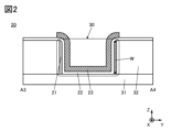
- FIG. 2 is a cross-sectional view showing an example of a semiconductor device.
- 3A and 3B are schematic perspective and plan views illustrating an example of a semiconductor device.
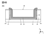
- 4A and 4B are cross-sectional views showing an example of a semiconductor device.
- 5A and 5B are cross-sectional views showing an example of a semiconductor device.
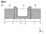
- 6A and 6B are cross-sectional views showing an example of a semiconductor device.
- 7A and 7B are schematic perspective and plan views illustrating an example of a semiconductor device.
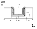
- 8A and 8B are cross-sectional views showing an example of a semiconductor device.
- FIGS. 9A and 9B are schematic perspective and cross-sectional views illustrating an example of a semiconductor device.
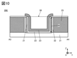
- FIG. 10 is a cross-sectional view showing an example of a semiconductor device.
- 11A is a plan view illustrating an example of a semiconductor device
- FIG.11B is a cross-sectional view illustrating an example of a semiconductor device.
- FIG. 12 is a cross-sectional view showing an example of a semiconductor device.
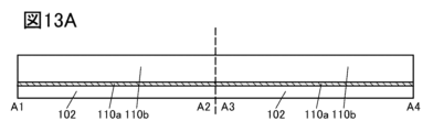
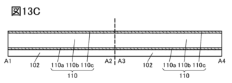
- 13A to 13C are cross-sectional views showing an example of a method for manufacturing a semiconductor device.
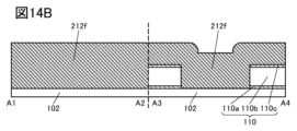
- 14A to 14C are cross-sectional views showing an example of a method for manufacturing a semiconductor device.
- 15A to 15C are cross-sectional views showing an example of a method for manufacturing a semiconductor device.
- FIG. 16A and 16B are cross-sectional views illustrating an example of a method for manufacturing a semiconductor device.
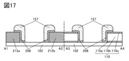
- 17A to 17C are cross-sectional views illustrating an example of a method for manufacturing a semiconductor device.
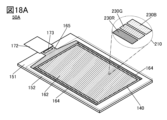
- Fig. 18A is a perspective view showing an example of a display device
- Fig. 18B is a block diagram showing an example of the display device.
- Fig. 19A is a circuit diagram of a latch circuit
- Fig. 19B is a circuit diagram of an inverter circuit.
- 20A and 20B are circuit diagrams of a pixel circuit
- Fig. 20C is a cross-sectional view showing an example of a pixel circuit.
- FIG. 21 is a schematic cross-sectional view showing a configuration example of a display device.
- 22A and 22B are diagrams illustrating an example of the configuration of an electronic device.
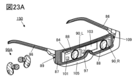
- 23A and 23B are diagrams illustrating an example of the configuration of an electronic device.
- 24A and 24B are diagrams illustrating a configuration example of a display device.
- FIG. 25 is a diagram illustrating an example of the configuration of a display device.
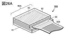
- 26A to 26C are perspective views of a display module.
- 27A and 27B are diagrams illustrating a configuration example of a display device.
- 28A to 28D are circuit diagrams of pixel circuits.
- 29A to 29D are circuit diagrams of pixel circuits.
- 30A and 30B are diagrams illustrating a configuration example of a display device.
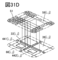
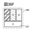
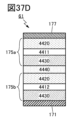
- 31A to 31D are diagrams for explaining a configuration example of a display device.
- an identification reference number such as “_1”, “[n]”, “[m,n]” may be added to the reference number.
- an identification reference number such as “_1”, “[n]”, “[m,n]” is added to a reference number in a drawing, etc., when it is not necessary to distinguish between them in this specification, the identification reference number may not be added.
- ordinal numbers “first” and “second” are used for convenience and do not limit the number of components or the order of the components (e.g., process order or stacking order).
- an ordinal number attached to a component in one place in this specification may not match an ordinal number attached to the same component in another place in this specification or in the claims.
- film and “layer” can be interchanged depending on the circumstances.
- conductive layer can be changed to the term “conductive film.”
- insulating film can be changed to the term “insulating layer.”
- a transistor is a type of semiconductor element that can perform functions such as amplifying current or voltage, and switching operations that control conduction or non-conduction.
- transistor includes IGFETs (Insulated Gate Field Effect Transistors) and thin film transistors (TFTs).
- source and drain may be interchanged when transistors of different polarity are used, or when the direction of current changes during circuit operation. For this reason, in this specification, the terms “source” and “drain” may be used interchangeably. Note that the source and drain of a transistor may be appropriately referred to as the source terminal and drain terminal, or the source electrode and drain electrode, depending on the situation.
- Gate and backgate can be used interchangeably. For this reason, in this specification and the like, the terms “gate” and “backgate” can be used interchangeably. Note that the names of the gate and backgate of a transistor can be appropriately changed depending on the situation, such as gate electrode and backgate electrode.
- electrically connected includes cases where the connection is made via "something that has some kind of electrical action.”
- something that has some kind of electrical action is not particularly limited as long as it allows the transmission and reception of electrical signals between the connected objects.
- something that has some kind of electrical action includes electrodes or wiring, as well as switching elements such as transistors, resistive elements, coils, and other elements with various functions.
- the off-state current refers to leakage current between the source and drain when a transistor is in an off state (also referred to as a non-conducting state or a cut-off state).
- the off-state refers to a state in which the voltage Vgs between the gate and source of an n-channel transistor is lower than the threshold voltage Vth (higher than Vth for a p-channel transistor).
- top surface shapes roughly match means that at least a portion of the contours of the stacked layers overlap. For example, this includes cases where the upper and lower layers are processed using the same mask pattern, or where parts of the mask pattern are the same. However, strictly speaking, the contours may not overlap, and the upper layer may be located inside the lower layer, or outside the lower layer, in which case it may also be said that “top surface shapes roughly match.” Furthermore, when the top surface shapes match or roughly match, it can also be said that the edges are aligned or roughly aligned.
- the top surface shape of a certain component refers to the contour shape of the component when viewed from a plan view.
- a plan view refers to a view from the normal direction of the surface on which the component is formed, or the surface of the support (e.g., substrate) on which the component is formed.
- a tapered shape refers to a shape in which at least a portion of the side of the structure is inclined with respect to the substrate surface or the surface to be formed.
- it refers to a shape in which the angle (also called the taper angle) between the inclined side and the substrate surface or the surface to be formed is less than 90°.
- the side of the structure, the substrate surface, and the surface to be formed do not necessarily need to be completely flat, and may be approximately planar with a slight curvature, or approximately planar with fine irregularities.
- a device manufactured using a metal mask or an FMM may be referred to as a device with an MM (metal mask) structure.
- a device manufactured without using a metal mask or an FMM may be referred to as a device with an MML (metal maskless) structure.
- devices with an MML structure can be manufactured without using a metal mask, they can exceed the upper limit of fineness resulting from the alignment accuracy of the metal mask.
- devices with an MML structure can eliminate the need for equipment related to the manufacturing of metal masks and the process of cleaning the metal masks.
- devices with an MML structure are suitable for mass production because they make it possible to keep manufacturing costs low.
- a light-emitting device (also referred to as a light-emitting element) has an EL layer between a pair of electrodes.
- the EL layer has at least a light-emitting layer.
- layers also referred to as functional layers
- a light-receiving device (also referred to as a light-receiving element) has at least an active layer that functions as a photoelectric conversion layer between a pair of electrodes.
- one of the pair of electrodes may be referred to as a pixel electrode, and the other as a common electrode.
- island-like refers to a state in which two or more layers made of the same material and formed in the same process are physically separated.
- step discontinuity refers to the phenomenon in which a layer, film, or electrode is divided due to the shape of the surface on which it is formed (e.g., a step, etc.).
- the side of the insulating layer in the opening located between the source electrode and the drain electrode functions as a channel formation region of the transistor.
- the distance between the source electrode and the drain electrode on the side corresponds to the channel length of the transistor
- the depth (height) of the side corresponds to the channel width of the transistor. Therefore, by adjusting the thickness of the insulating layer in which the source electrode and the drain electrode are embedded, the channel width of the transistor changes, and the on-current of the transistor can be adjusted.
- the thinner the insulating layer the smaller the channel width of the transistor, and the smaller the ratio of the channel width to the channel length of the transistor can be. This allows the on-current of the transistor to be reduced.
- the thicker the insulating layer the larger the channel width of the transistor, and the larger the ratio of the channel width to the channel length of the transistor can be. This allows the on-current of the transistor to be increased.
- the semiconductor device 20 can control the channel width W of the transistor included in the semiconductor device by the thickness of the insulating layer 32 (the depth of the opening 30). That is, the contact area between the semiconductor layer 21 and the conductive layer 24a and the conductive layer 24b (the area of the side surface of the conductive layer 24a and the conductive layer 24b at the opening 30 shown in FIG. 1A) can be adjusted by the thickness of the insulating layer 32. In other words, the channel width W of the transistor can be adjusted by the thickness of the insulating layer 32.
- the length (D1) of the opening 30 in the Y direction (A3-A4 direction) is approximately equal to the length (D2) of the conductive layers 24a and 24b (FIG. 1A).
- the length (D1) of the opening 30 in the Y direction (A3-A4 direction) is longer than the length (D2) of the conductive layers 24a and 24b (FIGS. 3A and 3B).
- the channel width W is illustrated as being the same for both the transistors in semiconductor device 20 and the transistors in semiconductor device 20A. Therefore, in terms of the W/L ratio, the transistors in semiconductor device 20A are smaller than the transistors in semiconductor device 20. In other words, it can be said that semiconductor device 20A has transistors with smaller on-currents than semiconductor device 20.
- the semiconductor device 20B can have a larger contact area between the semiconductor layer 21 and the conductive layers 24a and 24b than the semiconductor device 20. That is, the semiconductor device 20B can have a transistor with a larger on-current than the semiconductor device 20. Furthermore, in the semiconductor device 20B, the contact area between the semiconductor layer 21 and other layers (conductive layers 24a, 24b, insulating layer 32, and insulating layer 31) is larger than that of the semiconductor device 20, so that peeling of the semiconductor layer 21 can be suppressed. Therefore, the semiconductor device can be manufactured with high productivity and high yield.
- FIGS. 6A and 6B show an example of the configuration of a semiconductor device 20C having a different configuration from the semiconductor device 20 shown in FIGS. 1B and 2.
- the schematic perspective view of the semiconductor device 20A shown in FIG. 3A can be referred to. That is, the conductive layer 24a, the conductive layer 24b, and the insulating layer 32 have the same configuration in the semiconductor device 20A and the semiconductor device 20C.
- FIG. 6A is a cross-sectional view taken along dashed line A1-A2 shown in FIG. 3A.
- FIG. 6B is a cross-sectional view taken along dashed line A3-A4 shown in FIG. 3A.
- some components of the semiconductor device 20C are omitted in FIG. 3A.
- the following section will mainly explain the differences between semiconductor device 20C and semiconductor device 20, and may omit explanations of overlapping parts.
- semiconductor device 20C can enjoy both the effects obtained by semiconductor device 20A and the effects obtained by semiconductor device 20B.
- opening 30 may have a top surface shape other than a rectangle. This allows for greater freedom in the processing shape of opening 30, and therefore allows for improved integration of transistors when manufacturing a semiconductor device having multiple transistors within a substrate surface.
- the upper surface shape of the opening 30 is shown as a rectangle, but as in the semiconductor device 20D, the upper surface shape of the opening 30 may be a circle.
- the upper surface shape of the opening 30 is not limited to the above, and may be various shapes. For example, it may be an ellipse, a rectangle with rounded corners, etc. It may also be a regular polygon such as an equilateral triangle, a square, a regular pentagon, or a polygon other than a regular polygon.
- the contents described above for the semiconductor device 20 and the like can also be applied to the semiconductor device described later.
- the contents described for the semiconductor device described later can also be applied to the semiconductor device 20 and the like.
- an oxynitride refers to a material whose composition contains more oxygen than nitrogen.
- An oxynitride refers to a material whose composition contains more nitrogen than oxygen.
- oxygen can be supplied to the semiconductor layer 208.
- oxygen vacancies (V O ) are repaired and the oxygen vacancies (V O ) can be reduced. Therefore, a transistor having good electrical characteristics and high reliability can be obtained.
- a film that is difficult for oxygen to permeate for each of the insulating layers 110a and 110c can suppress the oxygen contained in the insulating layer 110b from diffusing to the substrate 102 side through the insulating layer 110a. Similarly, it can suppress the oxygen contained in the insulating layer 110b from diffusing to the insulating layer 106 side through the insulating layer 110c.
- the insulating layer 110a and the insulating layer 110c each preferably contain nitrogen, and preferably use one or more of the above-mentioned nitrides and nitride oxides.
- silicon nitride or silicon nitride oxide may be preferably used for the insulating layer 110a and the insulating layer 110c, respectively.
- one or both of the insulating layer 110a and the insulating layer 110c may use one or more of an oxide and an oxynitride.
- aluminum oxide may be preferably used for the insulating layer 110a and the insulating layer 110c, respectively.
- the insulating layer 110a may use the same material as the insulating layer 110c, or a different material may be used.
- the thickness T110a of the insulating layer 110a is large, the amount of impurities released from the insulating layer 110a may increase, resulting in a large amount of impurities diffusing into the channel formation region.
- the thickness T110a is small, oxygen contained in the insulating layer 110b may diffuse to the substrate 102 side through the insulating layer 110a, resulting in a decrease in the amount of oxygen supplied to the channel formation region.
- the thickness T110b of the insulating layer 110b can be, for example, 5 nm or more and less than 3 ⁇ m, 7 nm or more and less than 2.5 ⁇ m, 10 nm or more and less than 2 ⁇ m, 10 nm or more and less than 1.5 ⁇ m, 10 nm or more and less than 1.2 ⁇ m, 10 nm or more and less than 1 ⁇ m, 10 nm or more and less than 500 nm, 10 nm or more and less than 300 nm, 10 nm or more and less than 200 nm, 10 nm or more and less than 100 nm, 10 nm or more and less than 50 nm, 10 nm or more and less than 30 nm, or 10 nm or more and less than 20 nm.
- the diameter of the opening 145 in plan view is equal to or greater than the limit resolution of the exposure device.
- the diameter of the opening 145 can be, for example, 200 nm or more and less than 5 ⁇ m, 300 nm or more and less than 4.5 ⁇ m, 400 nm or more and less than 4 ⁇ m, 500 nm or more and less than 3.5 ⁇ m, 500 nm or more and less than 3 ⁇ m, 500 nm or more and less than 2.5 ⁇ m, 500 nm or more and less than 2 ⁇ m, 500 nm or more and less than 1.5 ⁇ m, or 500 nm or more and less than 1 ⁇ m.
- the insulating layer 110a and the insulating layer 110c are made of a material that releases less hydrogen from itself.
- the insulating layer 110a and the insulating layer 110c are made of a material that releases even a small amount of hydrogen, it is preferable that the thicknesses of these layers are thin.
- the channel length L200 and the channel width W200 of the transistors included in the semiconductor device 200 of one embodiment of the present invention can be adjusted by varying the thickness of the insulating layer 110 and the top surface shape of the opening 145.
- the W/L ratio by adjusting the W/L ratio by varying the thickness of the insulating layer 110 and the top surface shape of the opening 145, a transistor with a large W/L ratio can be applied to a transistor that requires a large on-current, and a transistor with a small W/L ratio can be applied to a transistor that requires high saturation, thereby realizing a high-performance semiconductor device 200 that makes use of the advantages of each transistor.
- the element M include aluminum, gallium, tin, yttrium, titanium, vanadium, chromium, manganese, iron, cobalt, nickel, zirconium, molybdenum, hafnium, tantalum, tungsten, lanthanum, cerium, neodymium, magnesium, calcium, strontium, barium, boron, silicon, germanium, and antimony.
- the element M of the metal oxide is preferably one or more of the above elements, more preferably one or more selected from aluminum, gallium, tin, and yttrium, and even more preferably one or more of gallium and tin.
- metal elements and metalloid elements may be collectively referred to as "metal elements", and the "metal element" described in this specification may include metalloid elements.
- the semiconductor layer 208 may be, for example, indium oxide (In oxide), indium zinc oxide (In-Zn oxide), indium tin oxide (In-Sn oxide, also referred to as ITO), indium titanium oxide (In-Ti oxide), indium gallium oxide (In-Ga oxide), indium tungsten oxide (In-W oxide, also referred to as IWO), indium gallium aluminum oxide (In-Ga-Al oxide), indium gallium tin oxide (In-Ga-Sn oxide), gallium zinc oxide (Ga-Zn oxide, also referred to as GZO), aluminum zinc oxide (Al-Zn oxide, AZ), or O), indium aluminum zinc oxide (In-Al-Zn oxide, also referred to as IAZO), indium tin zinc oxide (In-Sn-Zn oxide, also referred to as ITZO (registered trademark)), indium titanium zinc oxide (In-Ti-Zn oxide), indium gallium zinc oxide (In-Ga-Zn oxide, also
- indium tin oxide containing silicon also referred to as ITSO
- gallium tin oxide Ga-Sn oxide
- aluminum tin oxide Al-Sn oxide
- materials not containing Zn such as indium oxide, are suitable because they have high affinity with Si processes.
- materials containing Zn are suitable because they can improve crystallinity.
- the field effect mobility of the transistor can be increased.
- a transistor with a large on-current can be realized.
- the metal elements include yttrium, zirconium, silver, cadmium, tin, antimony, barium, lead, bismuth, lanthanum, cerium, praseodymium, neodymium, promethium, samarium, and europium.
- Lanthanum, cerium, praseodymium, neodymium, promethium, samarium, and europium are called light rare earth elements.
- the metal oxide becomes highly crystalline and the diffusion of impurities in the metal oxide can be suppressed. This suppresses fluctuations in the electrical characteristics of the transistor and increases its reliability.
- the electrical characteristics and reliability of the transistor vary depending on the composition of the metal oxide applied to the semiconductor layer 208. Therefore, by varying the composition of the metal oxide according to the electrical characteristics and reliability required of the transistor, a semiconductor device that combines excellent electrical characteristics and high reliability can be obtained.
- the metal oxide is an In-M-Zn oxide
- the atomic ratio of In in the In-M-Zn oxide is equal to or greater than the atomic ratio of element M.
- the atomic ratio of In in the In-M-Zn oxide may be less than the atomic ratio of the element M.
- the ratio of the number of indium atoms to the sum of the numbers of atoms of all metal elements contained may be referred to as the indium content. The same applies to other metal elements.
- the on-current or field effect mobility of the transistor can be increased. Furthermore, by having the element M, the generation of oxygen vacancies (V 0 ) can be suppressed.
- the element M is preferably one or more of the above elements, and more preferably one or more selected from aluminum, gallium, tin, and yttrium.
- In:Al:Zn 40:1:10 and metal oxides in the vicinity thereof can be preferably used.
- the silicon content (the ratio of the number of silicon atoms to the sum of the numbers of atoms of all metal elements contained) is preferably 1% or more and 20% or less, more preferably 3% or more and 20% or less, even more preferably 3% or more and 15% or less, and even more preferably 5% or more and 15% or less.
- the composition of the semiconductor layer 208 can be analyzed using, for example, energy dispersive X-ray spectrometry (EDX), X-ray photoelectron spectrometry (XPS), inductively coupled plasma mass spectrometry (ICP-MS), or inductively coupled plasma-atomic emission spectrometry (ICP-AES).
- EDX energy dispersive X-ray spectrometry
- XPS X-ray photoelectron spectrometry
- ICP-MS inductively coupled plasma mass spectrometry
- ICP-AES inductively coupled plasma-atomic emission spectrometry
- a combination of these techniques may be used for the analysis.
- the actual content may differ from the content obtained by analysis due to the influence of analytical accuracy. For example, if the content of element M is low, the content of element M obtained by analysis may be lower than the actual content.
- the sputtering method or the ALD method can be suitably used to form the metal oxide.
- the composition of the formed metal oxide may differ from the composition of the sputtering target.
- the zinc content in the formed metal oxide may decrease to about 50% compared to the sputtering target.
- the crystallinity of the semiconductor layer 208 can be analyzed, for example, by X-ray diffraction (XRD), a transmission electron microscope (TEM), or electron diffraction (ED). Alternatively, the analysis may be performed by combining a plurality of these techniques.
- XRD X-ray diffraction
- TEM transmission electron microscope
- ED electron diffraction
- VOH When a metal oxide is used for the semiconductor layer 208, it is preferable to reduce VOH in the channel formation region as much as possible to make it highly pure or substantially highly pure.
- it is important to remove impurities such as water and hydrogen in the metal oxide (sometimes referred to as dehydration or dehydrogenation treatment) and to supply oxygen to the metal oxide to repair oxygen vacancies ( VOH ).
- impurities such as water and hydrogen in the metal oxide
- VOH oxygen vacancies
- supplying oxygen to a metal oxide to repair oxygen vacancies ( VOH ) may be referred to as oxygen addition treatment.
- the semiconductor layer 208 may have a layered material that functions as a semiconductor.
- a layered material is a general term for a group of materials that have a layered crystal structure.
- a layered crystal structure is a structure in which layers formed by covalent or ionic bonds are stacked via bonds weaker than covalent or ionic bonds, such as van der Waals bonds.
- a layered material has high electrical conductivity within a unit layer, that is, high two-dimensional electrical conductivity.
- the conductive layer 212a, the conductive layer 212b, and the conductive layer 204 may each have a single layer structure or a laminated structure of two or more layers.
- Examples of materials that can be used for the conductive layer 212a, the conductive layer 212b, and the conductive layer 204 include one or more of chromium, copper, aluminum, gold, silver, zinc, tantalum, titanium, tungsten, manganese, nickel, iron, cobalt, molybdenum, and niobium, and alloys containing one or more of the above-mentioned metals.
- the conductive layer 212a, the conductive layer 212b, and the conductive layer 204 can each be preferably made of a low-resistance conductive material containing one or more of copper, silver, gold, and aluminum. In particular, copper or aluminum is preferable because of its excellent mass productivity.
- the insulating layer 106 has a single-layer structure, it is preferable to use an oxide or an oxynitride for the insulating layer 106. Specifically, silicon oxide or silicon oxynitride can be suitably used for the insulating layer 106.
- the thickness of the gate insulating layer becomes thin, the leakage current may become large.
- a material with a high relative dielectric constant also called a high-k material
- high-k materials that can be used for the insulating layer 106 include gallium oxide, hafnium oxide, zirconium oxide, oxides containing aluminum and hafnium, oxynitrides containing aluminum and hafnium, oxides containing silicon and hafnium, oxynitrides containing silicon and hafnium, and nitrides containing silicon and hafnium.
- FIGS. 13A to 17 show a cross-sectional view between dashed dotted lines A1-A2 and A3-A4 shown in FIG. 11A.
- the thin films (insulating films, semiconductor films, conductive films, etc.) that make up semiconductor devices can be formed by wet film formation methods such as spin coating, dipping, spray coating, inkjet, dispensing, screen printing, offset printing, doctor knife, slit coating, roll coating, curtain coating, or knife coating.
- the light used for exposure can be, for example, i-line (wavelength 365 nm), g-line (wavelength 436 nm), h-line (wavelength 405 nm), or a mixture of these. Other light such as ultraviolet light, KrF laser light, or ArF laser light can also be used.
- Exposure can also be performed by immersion exposure technology. Extreme ultraviolet (EUV) light or X-rays can also be used as the light used for exposure. Electron beams can also be used instead of the light used for exposure. Extreme ultraviolet light, X-rays, or electron beams are preferable because they enable extremely fine processing. When exposure is performed by scanning a beam such as an electron beam, a photomask is not required.
- the insulating layer 110a and the insulating layer 110b can be preferably formed by sputtering or PECVD. After forming the insulating layer 110a, it is preferable to form the insulating layer 110b continuously in a vacuum without exposing the surface of the insulating layer 110a to the atmosphere. By forming the insulating layer 110a and the insulating layer 110b continuously, it is possible to prevent impurities from the atmosphere from adhering to the surface of the insulating layer 110a. Examples of such impurities include water and organic matter.
- the substrate temperature during the formation of the insulating layer 110a and the insulating layer 110b is preferably 180°C or higher and 450°C or lower, more preferably 200°C or higher and 450°C or lower, even more preferably 250°C or higher and 450°C or lower, even more preferably 300°C or higher and 450°C or lower, even more preferably 300°C or higher and 400°C or lower, even more preferably 350°C or higher and 400°C or lower.
- the substrate temperature during the formation of the film is preferably 350°C or less, more preferably 340°C or less, even more preferably 330°C or less, and even more preferably 300°C or less. This allows a large amount of oxygen to be supplied to the insulating layer 110b.
- the film is removed.
- a wet etching method can be suitably used to remove the film.
- the film may be removed by a CMP process.
- the process of supplying oxygen to the insulating layer 110b is not limited to the above-mentioned method.
- oxygen radicals, oxygen atoms, oxygen atomic ions, or oxygen molecular ions are supplied to the insulating layer 110b by ion doping, ion implantation, or plasma treatment.
- oxygen may be supplied to the insulating layer 110b through the film. It is preferable to remove the film after supplying oxygen.
- a conductive film 212f which will later become conductive layer 212a and conductive layer 212b, is formed on the substrate 102 and on the insulating layer 110 so as to fill the opening 144 (FIG. 14B).
- a sputtering method can be suitably used to form the conductive film 212f.
- a resist mask 159 is formed on the conductive layer 212s and the insulating layer 110c.
- the resist mask 159 is provided so as to have an area that overlaps with the area in which the conductive layer 212a and the conductive layer 212b will be formed later.
- the conductive layer 212s is processed to form an opening 145 that reaches the substrate 102, and conductive layers 212a and 212b that sandwich the opening 145 (FIG. 15A).
- a wet etching method and a dry etching method can be suitably used.
- an anisotropic dry etching method can be suitably used.
- a fine opening 145 whose side is approximately perpendicular to the substrate surface can be formed, so that the area occupied by the transistor to be formed later in the substrate surface can be reduced. Note that this processing may result in the film thickness of the substrate 102 in the region overlapping with the opening 145 being thinner than the film thickness of the substrate 102 in the region not overlapping with the opening 145.
- the metal oxide film 208f is preferably formed by a sputtering method using a metal oxide target.
- the metal oxide film 208f is preferably formed by an ALD method.
- the ALD method has high coverage and can be suitably used to form the metal oxide film 208f that covers the opening 145.
- a metal oxide film can be formed with good coverage even on the side surface of the insulating layer 110.
- the ALD method makes it easy to control the film thickness by the number of cycles, so a thin film can be formed with good yield.
- the metal oxide film 208f is preferably a dense film with as few defects as possible.
- the metal oxide film 208f is preferably a high-purity film with as few impurities, including hydrogen, as possible reduced.
- oxygen gas when forming the metal oxide film 208f.
- oxygen gas oxygen can be suitably supplied to the insulating layer 110.
- oxygen gas oxygen can be suitably supplied to the insulating layer 110b.
- the metal oxide film may become polycrystalline.
- the grain boundaries become the recombination centers, and carriers may be captured, resulting in a small on-current of the transistor. Therefore, it is preferable to adjust the oxygen flow ratio or oxygen partial pressure so that the metal oxide film 208f does not become polycrystalline. Since the ease with which the metal oxide film becomes polycrystalline differs depending on the composition of the metal oxide film, the oxygen flow ratio or oxygen partial pressure may be adjusted according to the composition of the metal oxide film 208f.
- the higher the substrate temperature when forming the metal oxide film the higher the crystallinity and the denser the metal oxide film will be.
- the lower the substrate temperature the lower the crystallinity and the higher the electrical conductivity of the metal oxide film will be.
- the method for processing the semiconductor layer 208 in the semiconductor device of one embodiment of the present invention is not limited to the above.
- the semiconductor layer 208 may be formed by etching the metal oxide film 208f through a resist mask.
- Figure 17 shows a method for forming the semiconductor layer 208 by etching through a resist mask 157.
- the resist mask 157 is preferably formed so as to overlap the area straddling both the inside and outside of the opening 145.
- an etching process on the metal oxide film 208f in this state, it is possible to form a semiconductor layer 208 (semiconductor layer 21 in the case of semiconductor device 20B) with one end located inside the opening 145 (opening 30 in the case of semiconductor device 20B) and the other end located outside, as in the semiconductor device 20B shown in Figures 5A and 5B.
- the etching process can be preferably performed using either or both of a wet etching method and a dry etching method.
- insulating layer 195 is formed to cover conductive layer 204 and insulating layer 106.
- the PECVD method can be suitably used to form insulating layer 195.
- the semiconductor device of one embodiment of the present invention can be used, for example, as one or both of the display portion 162 and the circuit portion 164 of the display device 50A.
- Light-emitting devices include, for example, self-luminous light-emitting devices such as LEDs, OLEDs (organic LEDs), and semiconductor lasers. LEDs can include, for example, mini LEDs and micro LEDs.
- one electrode functions as an anode and the other electrode functions as a cathode.
- transistor Tr33 It is preferable to use a transistor with a small off-state current for the transistor Tr33.
- An OS transistor can be suitably used for the transistor Tr33. This allows the latch circuit LAT to hold data for a long period of time. This reduces the frequency with which data is rewritten to the latch circuit LAT.
- writing data to the latch circuit LAT such that the signal input from terminal SP2 is output to terminal LIN may be simply referred to as "writing data to the latch circuit LAT.”
- writing data with a value of "1" to the latch circuit LAT may be simply referred to as "writing data to the latch circuit LAT.”
- the inverter circuit INV has transistors Tr41, Tr43, Tr45, Tr47, and a capacitance element C41.
- all the transistors in the latch circuit LAT can be transistors of the same polarity, for example, n-channel transistors. This allows, for example, transistor Tr33 as well as transistors Tr31, Tr35, Tr36, Tr41, Tr43, Tr45, and Tr47 to be OS transistors. Therefore, all the transistors in the latch circuit LAT can be manufactured in the same process.
- the semiconductor device of one embodiment of the present invention can be preferably used for the inverter circuit INV.
- a VLFET included in the semiconductor device of one embodiment of the present invention can be applied to one or more of the transistors Tr41, Tr43, Tr45, and Tr47.
- ⁇ Configuration Example 3> 20A shows an example of the configuration of a pixel 230.
- the pixel 230 includes a pixel circuit 51 and a light-emitting device 61.
- the pixel circuit 51 shown in FIG. 20A is a 2Tr1C type pixel circuit having a transistor 52A, a transistor 52B, and a capacitor 53. Note that there is no particular limitation on the pixel circuit that can be applied to the display device of one embodiment of the present invention.
- the anode of the light-emitting device 61 is electrically connected to one of the source or drain of the transistor 52B and one electrode of the capacitance element 53.
- the other of the source or drain of the transistor 52B is electrically connected to the wiring ANO.
- the gate of the transistor 52B is electrically connected to one of the source or drain of the transistor 52A and the other electrode of the capacitance element 53.
- the other of the source or drain of the transistor 52A is electrically connected to the wiring GL.
- the gate of the transistor 52A is electrically connected to the wiring GL.
- the cathode of the light-emitting device 61 is electrically connected to the wiring VCOM.
- the pixel circuit 51A shown in FIG. 20B differs from the pixel circuit 51 shown in FIG. 20A mainly in that it has a transistor 52C.
- the pixel circuit 51A is a 3Tr1C type pixel circuit having a transistor 52A, a transistor 52B, a transistor 52C, and a capacitance element 53.
- the transistor 52C has a function of controlling the conductive state or non-conductive state between the wiring V0 and one of the source electrode or drain electrode of the transistor 52B based on the potential of the wiring GL.
- the reference potential of the wiring V0 provided via the transistor 52C can suppress variations in the gate-source voltage of the transistor 52B.
- the wiring V0 can be used to obtain a current value that can be used to set pixel parameters. Specifically, the wiring V0 can function as a monitor line for outputting the current flowing through the transistor 52B or the current flowing through the light-emitting device 61 to the outside.
- the current output to the wiring V0 can be converted to a voltage by a source follower circuit and output to the outside, or it can be converted to a digital signal by an AD converter and output to the outside.
- An insulating layer 195 is provided to cover the transistor 52A, the transistor 52B, and the capacitor 53, an insulating layer 233 is provided to cover the insulating layer 195, and an insulating layer 235 is provided to cover the insulating layer 233.
- a light-emitting device 61 can be provided on the insulating layer 235.
- FIG. 20C shows a pixel electrode 111 that functions as one electrode of the light-emitting device 61.
- the insulating layer 195 and the insulating layer 233 have a first opening that reaches the conductive layer 212a, and a conductive layer 234 is provided to cover the first opening.
- the conductive layer 234 is electrically connected to the conductive layer 212a through the first opening.
- the insulating layer 235 has a second opening that reaches the conductive layer 234, and a pixel electrode 111 is provided to cover the second opening.
- the pixel electrode 111 is electrically connected to the conductive layer 234 through the second opening.
- the insulating layer 195 can be described above, so a detailed description will be omitted.
- the insulating layer 233 and the insulating layer 235 have the function of reducing unevenness caused by the transistor 52A, the transistor 52B, and the transistor 52C, and making the surface on which the light-emitting device 61 is formed more flat. Note that in this specification and the like, the insulating layer 233 and the insulating layer 235 may each be referred to as a flattening layer.
- the insulating layer 233 and the insulating layer 235 are preferably organic insulating films.
- Materials that can be used for the organic insulating film include acrylic resin, polyimide resin, epoxy resin, polyamide resin, polyimideamide resin, siloxane resin, benzocyclobutene resin, phenol resin, and precursors of these resins.
- the insulating layer 235 may have a laminated structure of an organic insulating film and an inorganic insulating film. It is preferable that the insulating layer 235 has a laminated structure of an organic insulating film and an inorganic insulating film on the organic insulating film. This allows the inorganic insulating film to function as an etching protection layer when forming the light-emitting device 61.
- the display device 50B has a configuration in which a pixel circuit, a driver circuit, and the like are provided on a substrate 310.
- the display device 50B has an element layer 71, an element layer 73, an element layer 75, and a wiring layer 77.
- the wiring layer 77 is a layer in which wirings are provided.
- the element layer 71 has a substrate 310, and a transistor 300 is formed on the substrate 310.
- a wiring layer 77 is provided above the transistor 300, and wiring layer 77 has wiring that electrically connects the transistor 300, the transistor MTCK, the light-emitting device 130R, the light-emitting device 130G, and the light-emitting device 130B.
- An element layer 73 and an element layer 75 are provided above the wiring layer 77, and the element layer 73 has the transistor MTCK and the like.
- the element layer 75 has the light-emitting device 130 (in FIG. 21, the light-emitting device 130R, the light-emitting device 130G, and the light-emitting device 130B) and the like.
- Transistor 300 can be a transistor included in element layer 71.
- Transistor MTCK can be a transistor included in element layer 73.
- Light-emitting device 130 can be a light-emitting device included in element layer 75.
- the substrate 310 may be a semiconductor substrate (for example, a single crystal substrate made of silicon or germanium).
- the substrate 310 may be, for example, an SOI (Silicon On Insulator) substrate, a glass substrate, a quartz substrate, a plastic substrate, a sapphire glass substrate, a metal substrate, a stainless steel substrate, a substrate having stainless steel foil, a tungsten substrate, a substrate having tungsten foil, a flexible substrate, a laminated film, paper containing a fibrous material, or a base film.
- the substrate 310 is described as a semiconductor substrate having silicon as a material. Therefore, the transistors included in the element layer 71 may be Si transistors.
- the transistor 300 has an element isolation layer 312, a conductive layer 316, an insulating layer 315, an insulating layer 317, a semiconductor region 313 formed of a part of the substrate 310, and a low-resistance region 314a and a low-resistance region 314b that function as a source region or a drain region. Therefore, the transistor 300 is a Si transistor. Note that FIG.
- the display device of one embodiment of the present invention may have a configuration in which, for example, the gate of the transistor 300 is electrically connected to the conductive layer 514 via the conductive layer 328.
- the transistor 300 can be made into a Fin type by, for example, configuring the upper surface and the side surface in the channel width direction of the semiconductor region 313 to cover the conductive layer 316 via an insulating layer 315 that functions as a gate insulating layer.
- the effective channel width can be increased, and the on characteristics of the transistor 300 can be improved.
- the contribution of the electric field of the gate electrode can be increased, and therefore the off characteristics of the transistor 300 can be improved.
- the transistor 300 may be a planar type instead of a Fin type.
- the region in which the channel of the semiconductor region 313 is formed, the region nearby, and the low resistance region 314a and low resistance region 314b that become the source region or drain region preferably contain a silicon-based semiconductor, specifically, single crystal silicon.
- each of the above-mentioned regions may be formed using, for example, germanium, silicon germanium, gallium arsenide, aluminum gallium arsenide, or gallium nitride.
- a configuration using silicon in which the effective mass is controlled by applying stress to the crystal lattice and changing the lattice spacing may also be used.
- the transistor 300 may be, for example, a HEMT (High Electron Mobility Transistor) using gallium arsenide and aluminum gallium arsenide.
- HEMT High Electron Mobility Transistor
- the conductive layer 316 which functions as a gate electrode, can be made of a semiconductor material such as silicon containing an element that imparts n-type conductivity, such as arsenic or phosphorus, or an element that imparts p-type conductivity, such as boron or aluminum.
- the conductive layer 316 can be made of a conductive material such as a metal material, an alloy material, or a metal oxide material.
- the work function is determined by the material of the conductor, so the threshold voltage of the transistor can be adjusted by selecting the material of the conductor. Specifically, it is preferable to use one or both of titanium nitride and tantalum nitride as the conductor. Furthermore, in order to achieve both conductivity and embeddability, it is preferable to use one or both of tungsten and aluminum as a laminated material for the conductor, and in particular, it is preferable to use tungsten in terms of heat resistance.
- the element isolation layer 312 is provided to isolate multiple transistors formed on the substrate 310 from each other.
- the element isolation layer can be formed, for example, by using a LOCOS (Local Oxidation of Silicon) method, a STI (Shallow Trench Isolation) method, or a mesa isolation method.
- LOCOS Local Oxidation of Silicon
- STI Shallow Trench Isolation
- an insulating layer 320 and an insulating layer 322 are stacked in this order from the substrate 310 side.
- Insulating layer 320 and insulating layer 322 may be made of, for example, one or more selected from silicon oxide, silicon oxynitride, silicon nitride oxide, silicon nitride, aluminum oxide, aluminum oxynitride, aluminum nitride oxide, and aluminum nitride.
- oxynitride refers to a material whose composition contains more oxygen than nitrogen
- nitride oxide refers to a material whose composition contains more nitrogen than oxygen
- silicon oxynitride refers to a material whose composition contains more oxygen than nitrogen
- silicon nitride oxide refers to a material whose composition contains more nitrogen than oxygen
- a conductive layer 328 is embedded in the insulating layer 320 and the insulating layer 322, and connects to the transistor MTCK and the like that are provided above the insulating layer 322.
- the conductive layer 328 functions as a plug or wiring.
- the conductive layer 328 can be made of a material that can be applied to the conductive layer MPG.
- a wiring layer 77 is provided on the transistor 300.
- the wiring layer 77 includes, for example, an insulating layer 324, an insulating layer 326, a conductive layer 330, an insulating layer 350, an insulating layer 352, an insulating layer 354, and a conductive layer 356.
- the conductive layer 330 and the conductive layer 356 function as a plug or wiring that connects to the transistor 300. Note that the conductive layer 330 and the conductive layer 356 can be formed using a material similar to that of the conductive layer 328 or the conductive layer 596 described above.
- an insulator having a barrier property against one or more selected from hydrogen, oxygen, and water for the insulating layer 324, the insulating layer 350, and the insulating layer 592. It is also preferable to use an insulator having a relatively low relative dielectric constant for the insulating layer 326, the insulating layer 352, the insulating layer 354, and the insulating layer 594 in order to reduce the parasitic capacitance generated between wirings.
- the insulating layer 326, the insulating layer 352, and the insulating layer 354 function as an interlayer insulating film and a planarizing film. It is also preferable that the conductive layer 356 contains a conductor having a barrier property against one or more selected from hydrogen, oxygen, and water.
- An insulating layer 512 is provided above the insulating layer 354 and the conductive layer 356.
- An insulating layer IS1 is provided on the insulating layer 512.
- a conductive layer 514 that functions as a plug or wiring is embedded in the insulating layer IS1 and the insulating layer 512. This electrically connects one of the source or drain of the transistor MTCK to one of the source or drain of the transistor 300.
- a material that can be used for the conductive layer MPG can be used for the conductive layer 514.
- An insulating layer IS3 is formed above the transistor MTCK.
- insulating layers 574 and 581 are stacked in this order on the insulating layer IS3.
- the insulating layer 574 preferably has a function of suppressing the diffusion of impurities such as water and hydrogen (e.g., hydrogen atoms and/or hydrogen molecules).
- the insulating layer 574 preferably functions as a barrier insulating film that suppresses the impurities from being mixed into the transistor MTCK.
- the insulating layer 574 also preferably has a function of suppressing the diffusion of oxygen (e.g., oxygen atoms and/or oxygen molecules).
- the insulating layer 574 preferably has lower oxygen permeability than the insulating layer IS2 and the insulating layer IS3.
- the insulating layer 574 preferably functions as a barrier insulating film that suppresses the diffusion of impurities such as water and hydrogen. Therefore, the insulating layer 574 is preferably made of an insulating material that has a function of suppressing the diffusion of impurities such as hydrogen atoms, hydrogen molecules, water molecules, nitrogen atoms, nitrogen molecules, nitrogen oxide molecules (e.g., N2O , NO, and NO2 ), and copper atoms (through which the above impurities are unlikely to permeate). Alternatively, it is preferable to use an insulating material that has a function of suppressing the diffusion of oxygen (e.g., oxygen atoms and/or oxygen molecules) (through which the above oxygen is unlikely to permeate).
- oxygen e.g., oxygen atoms and/or oxygen molecules
- Insulators having the function of suppressing the permeation of impurities such as water and hydrogen and oxygen may be used in a single layer or in a multilayer structure, and may contain one or more of boron, carbon, nitrogen, oxygen, fluorine, magnesium, aluminum, silicon, phosphorus, chlorine, argon, gallium, germanium, yttrium, zirconium, lanthanum, neodymium, hafnium, and tantalum.
- insulators having the function of suppressing the permeation of impurities such as water and hydrogen and oxygen may include metal oxides such as aluminum oxide, magnesium oxide, gallium oxide, germanium oxide, yttrium oxide, zirconium oxide, lanthanum oxide, neodymium oxide, hafnium oxide, and tantalum oxide.
- Insulators having the function of suppressing the permeation of impurities such as water and hydrogen and oxygen may include, for example, oxides containing aluminum and hafnium (hafnium aluminate).
- the insulating layer 574 it is preferable to use aluminum oxide or silicon nitride for the insulating layer 574. This can prevent impurities such as water and hydrogen from diffusing from above the insulating layer 574 to the transistor MTCK. Alternatively, it can prevent oxygen contained in the insulating layer IS3, etc. from diffusing above the insulating layer 574.
- the insulating layer 581 is a film that functions as an interlayer film, and preferably has a lower dielectric constant than the insulating layer 574.
- the relative dielectric constant of the insulating layer 581 is preferably less than 4, and more preferably less than 3.
- the relative dielectric constant of the insulating layer 581 is preferably 0.7 times or less the relative dielectric constant of the insulating layer 574, and more preferably 0.6 times or less.
- the insulating layer 581 preferably has a reduced concentration of impurities such as water and hydrogen in the film.
- the insulating layer 581 can be made of, for example, silicon oxide, silicon oxynitride, silicon nitride oxide, or silicon nitride.
- the insulating layer 581 can be made of, for example, silicon oxide to which fluorine has been added, silicon oxide to which carbon has been added, silicon oxide to which carbon and nitrogen have been added, or silicon oxide having vacancies.
- silicon oxide and silicon oxynitride are preferred because they are thermally stable.
- materials such as silicon oxide, silicon oxynitride, and silicon oxide having vacancies are preferred because they can easily form a region containing oxygen that is released by heating.
- the insulating layer 581 can be made of resin.
- the material that can be used for the insulating layer 581 may be an appropriate combination of the above-mentioned materials.
- Insulating layer 592 and insulating layer 594 are laminated in this order on insulating layer 574 and insulating layer 581.
- Insulating layer 598 and insulating layer 599 are formed on insulating layer 594 and conductive layer 596, in that order.
- the motion detection unit 101 has a function of detecting the movement of the housing 105, that is, the movement of the head of the user wearing the electronic device 150.
- the motion detection unit 101 may use, for example, a motion sensor using MEMS technology.
- a motion sensor using MEMS technology.
- a three-axis motion sensor or a six-axis motion sensor may be used.
- Information regarding the movement of the housing 105 detected by the motion detection unit 101 may be referred to as first information or motion information.
- the calculation unit 103 performs various data processing and program control by interpreting and executing commands from various programs using the processor.
- the programs that can be executed by the processor may be stored in a memory area of the processor, or may be stored in a separately provided storage unit.
- the storage unit for example, a storage device using non-volatile storage elements such as flash memory, MRAM (Magnetoresistive Random Access Memory), PRAM (Phase change RAM), ReRAM (Resistive RAM), and FeRAM (Ferroelectric RAM), or a storage device using volatile storage elements such as DRAM (Dynamic RAM) and SRAM (Static RAM) may be used.
- the electronic device 150 may be provided with a sensor 97.
- the sensor 97 may have a function of acquiring information on one or more of the user's vision, hearing, touch, taste, and smell. More specifically, the sensor 97 may have a function of detecting or measuring information on one or more of the following: force, displacement, position, speed, acceleration, angular velocity, rotation speed, distance, light, magnetism, temperature, sound, time, electric field, current, voltage, power, radiation, humidity, gradient, vibration, odor, and infrared light.
- the electronic device 150 may be provided with one or more sensors 97.
- the housing 105 shown in FIG. 23A is provided with an input terminal 109 and an output terminal 89.
- the input terminal 109 can be connected to a cable that supplies an image signal (image data) from a video output device or the like, or power for charging a battery (not shown) provided within the housing 105.
- the output terminal 89 functions as an audio output terminal, for example, and can be used to connect earphones, headphones, etc.
- the housing 105 preferably has a mechanism that allows the left-right positions of the lens 88 and the display devices 90_L and 90_R to be adjusted so that they are optimally positioned according to the position of the user's eyes. It is also preferable that the housing 105 has a mechanism that allows the focus to be adjusted by changing the distance between the lens 88 and the display devices 90_L and 90_R.
- the electronic device of one embodiment of the present invention may further include an earphone 99A.
- the earphone 99A has a communication unit (not shown) and has a wireless communication function.
- the earphone 99A can output audio data using the wireless communication function.
- the earphone 99A may also have a vibration mechanism that functions as a bone conduction earphone.
- the earphone 99A can be configured to be connected directly to the mounting portion 86 or connected via a wire, like the earphone 99B shown in FIG. 23B.
- the earphone 99B and the mounting portion 86 may also have a magnet. This allows the earphone 99B to be fixed to the mounting portion 86 by magnetic force, which is preferable as it makes storage easier.
- FIG. 24A, 24B, and 25 The configuration of a display device 90A that can be applied to the display device 90_L and the display device 90_R shown in FIGS. 22A and 22B will be described with reference to FIGS. 24A, 24B, and 25.
- FIG. 24A, 24B, and 25 The configuration of a display device 90A that can be applied to the display device 90_L and the display device 90_R shown in FIGS. 22A and 22B will be described with reference to FIGS. 24A, 24B, and 25.
- FIG. 24A is a perspective view of a display device 90A that can be used with the display devices 90_L and 90_R shown in FIGS. 22A and 22B.
- a display unit 93 capable of displaying at a resolution of so-called full high vision (also called “2K resolution”, “2K1K”, or “2K”). Also, for example, when the pixels 230 are arranged in a matrix of 3840 x 2160 pixels, a display unit 93 capable of displaying at a resolution of so-called ultra high vision (also called “4K resolution”, “4K2K”, or “4K”).
- the pixel density (resolution) of the display unit 93 is preferably 1000 ppi or more and 10000 ppi or less. For example, it may be 2000 ppi or more and 6000 ppi or less, or 3000 ppi or more and 5000 ppi or less.
- the display unit 93 can support various screen ratios, such as 1:1 (square), 4:3, 16:9, and 16:10.
- a display element may sometimes be referred to as "device.”
- a display element, a light-emitting element, and a liquid crystal element may be referred to as a display device, a light-emitting device, and a liquid crystal device, respectively.
- the display device 90A receives various signals and power supply potentials from the outside via the terminal section 94, and can display images using the display elements provided in the display section 93.
- Various elements can be used as the display elements.
- Representative examples include light-emitting elements that have the function of emitting light, such as organic EL elements (OLED elements) and LED elements, liquid crystal elements, and MEMS (Micro Electro Mechanical Systems) elements.
- a number of layers are provided between substrate 91 and substrate 92, and each layer is provided with transistors for performing circuit operations or display elements for emitting light.
- pixel circuits having the function of controlling the operation of the display elements
- drive circuits having the function of controlling the pixel circuits
- functional circuits having the function of controlling the drive circuits, etc. are provided.
- a layer 62 is provided on the substrate 91.
- the layer 62 has a driver circuit 65, a functional circuit 40, and an input/output circuit 80.
- the layer 62 has a transistor 63 (also called a Si transistor) having silicon in a channel formation region 64.
- a silicon substrate can be used for the substrate 91.
- a silicon substrate is preferable because it has higher thermal conductivity than a glass substrate.
- the transistor 63 can be, for example, a transistor having single crystal silicon in the channel formation region (also referred to as a c-Si transistor).
- a transistor having single crystal silicon in the channel formation region also referred to as a c-Si transistor.
- the on-state current of the transistor can be increased. This is preferable because the circuit in the layer 62 can be driven at high speed.
- a Si transistor can be formed by microfabrication so that the channel length is 3 nm or more and 10 nm or less, a display device 90A in which an accelerator such as a CPU or GPU, an application processor, etc. are provided integrally with the display unit can be used.
- a transistor having polycrystalline silicon in a channel formation region may be provided in layer 62.
- Low temperature polysilicon LTPS: Low Temperature Poly Silicon
- LTPS transistor a transistor having LTPS in a channel formation region
- an OS transistor may be provided in layer 62 as necessary.
- the driving circuit 65 has, for example, a gate driver circuit, a source driver circuit, and the like. In addition, it may have an arithmetic circuit, a memory circuit, a power supply circuit, and the like.
- the width of the non-display area (also called a frame) existing on the periphery of the display unit 93 of the display device 90A can be made extremely narrow compared to the case where these circuits and the display unit 93 are arranged side by side, and the display device 90A can be made smaller.
- the functional circuit 40 has, for example, the function of an application processor for controlling each circuit in the display device 90A and generating signals for controlling each circuit.
- the functional circuit 40 may also have a circuit for correcting image data such as an accelerator such as a CPU or GPU.
- the functional circuit 40 may also have an LVDS (Low Voltage Differential Signaling) circuit that functions as an interface for receiving image data from outside the display device 90A, a MIPI (Mobile Industry Processor Interface) circuit, and a D/A (Digital to Analog) conversion circuit.
- the functional circuit 40 may also have a circuit for compressing and expanding image data, a power supply circuit, etc.
- a layer 83 is provided on the layer 62.
- the layer 83 has a pixel circuit group 55 including a plurality of pixel circuits 51.
- An OS transistor may be provided in the layer 83.
- the pixel circuit 51 may be configured to include an OS transistor. Note that the layer 83 can be stacked on the layer 62.
- Si transistors may be provided in layer 83.
- pixel circuit 51 may be configured to include transistors having single crystal silicon or polycrystalline silicon in the channel formation region.
- LTPS may be used as the polycrystalline silicon.
- layer 83 may be formed on a separate substrate and bonded to layer 62.
- the pixel circuit 51 may be composed of multiple types of transistors using different semiconductor materials.
- the transistors may be provided in different layers for each type of transistor.
- the Si transistors and the OS transistors may be provided in a stacked state. By providing the transistors in a stacked state, the area occupied by the pixel circuit 51 is reduced. This can improve the resolution of the display device 90A.
- LTPO a configuration in which LTPS transistors and OS transistors are combined may be referred to as LTPO.
- the transistor 52 which is an OS transistor
- Such an OS transistor has a characteristic of having a very low off-state current. Therefore, it is particularly preferable to use an OS transistor as a transistor provided in a pixel circuit, because analog data written to the pixel circuit can be retained for a long period of time.
- Layer 81 is provided on layer 83.
- Substrate 92 is provided on layer 81.
- Substrate 92 is preferably a light-transmitting substrate or a layer made of a light-transmitting material.
- Layer 81 is provided with a plurality of light-emitting devices 61.
- layer 81 can be configured to be stacked on layer 83.
- organic electroluminescence elements also called organic EL elements
- light-emitting devices 61 are not limited to this, and for example, inorganic EL elements made of inorganic materials can be used.
- “organic EL elements” and “inorganic EL elements” may be collectively referred to as "EL elements”.
- Light-emitting devices 61 may have inorganic compounds such as quantum dots.
- quantum dots can be used in the light-emitting layer to function as light-emitting materials.
- the display device 90A can have a stacked configuration of the light-emitting device 61, the pixel circuit 51, the driver circuit 65, and the functional circuit 40, and therefore the aperture ratio (effective display area ratio) of the pixel can be extremely high.
- the aperture ratio of the pixel can be 40% or more and less than 100%, preferably 50% or more and 95% or less, and more preferably 60% or more and 95% or less.
- the pixel circuits 51 can be arranged at an extremely high density, and the resolution of the pixel can be extremely high.
- the display portion 93 (the region where the pixel circuits 51 and the light-emitting device 61 are stacked) of the display device 90A
- pixels with a resolution of 2000 ppi or more, preferably 3000 ppi or more, more preferably 5000 ppi or more, and even more preferably 6000 ppi or more, and 20000 ppi or less, or 30000 ppi or less.
- the diagonal size of the display unit 93 can be 0.1 inches or more and 5.0 inches or less, preferably 0.5 inches or more and 2.0 inches or less, and more preferably 1 inch or more and 1.7 inches or less.
- the diagonal size of the display unit 93 may be 1.5 inches or close to 1.5 inches.
- the display device 90A can be applied to devices other than wearable electronic devices.
- the diagonal size of the display portion 93 may exceed 2.0 inches.
- the configuration of the transistors used in the pixel circuit 51 may be appropriately selected according to the diagonal size of the display portion 93.
- the diagonal size of the display portion 93 is preferably 0.1 inches or more and 3 inches or less.
- the diagonal size of the display portion 93 is preferably 0.1 inches or more and 30 inches or less, and more preferably 1 inch or more and 30 inches or less.
- the diagonal size of the display portion 93 is preferably 0.1 inches or more and 50 inches or less, and more preferably 1 inch or more and 50 inches or less.
- the diagonal size of the display section 93 is preferably 0.1 inches or more and 200 inches or less, and more preferably 50 inches or more and 100 inches or less.
- a display device using single crystal Si transistors in the pixel circuit 51 etc. is difficult to handle large sizes (typically, screen sizes exceeding 30 inches in diagonal size) because a laser crystallization device is used in the manufacturing process.
- an OS transistor is not restricted by the use of a laser crystallization device in the manufacturing process, or can be manufactured at a relatively low process temperature (typically 450° C. or lower), so it is possible to handle display devices with a relatively large area (typically, diagonal size of 50 inches to 100 inches).
- LTPO can be applied to the diagonal size of the display part in the area between when an LTPS transistor is used and when an OS transistor is used (typically, 1 inch to 50 inches).
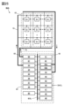
- FIG. 25 is a block diagram showing the configuration of the display device 90A, and shows the pixel circuits 51, the multiple wirings connecting the drive circuit 65 and the functional circuit 40, and the bus wiring within the display device 90A.
- the layer 83 has a plurality of pixel circuits 51 arranged in a matrix.
- the input/output circuit 80 supports transmission methods such as LVDS, and has a function of distributing control signals and image data input via a terminal unit 94 to a drive circuit 65 and a function circuit 40.
- the input/output circuit 80 also has a function of outputting information from the display device 90A to the outside via the terminal unit 94.
- the display device 90A in FIG. 25 illustrates a configuration in which the circuits included in the drive circuit 65, the circuits included in the functional circuit 40, and the input/output circuit 80 are each electrically connected to the bus wiring BSL.
- the source driver circuit 66 has a function of transmitting image data to the pixel circuit 51 of the pixel 230. Therefore, the source driver circuit 66 is electrically connected to the pixel circuit 51 via the wiring SL. Note that multiple source driver circuits 66 may be provided.
- the digital-to-analog conversion circuit 67 has a function of converting image data that has been digitally processed by a GPU, a correction circuit, etc., described below, into analog data.
- the image data converted into analog data is amplified by an amplifier circuit 35 such as an operational amplifier, and transmitted to the pixel circuit 51 via the source driver circuit 66. Note that the image data may be transmitted in the order of the source driver circuit 66, the digital-to-analog conversion circuit 67, and the pixel circuit 51.
- the digital-to-analog conversion circuit 67 and the amplifier circuit 35 may also be included in the source driver circuit 66.
- the functional circuit 40 may include a plurality of circuits capable of improving the display quality of the display device 90A.
- the circuit may include a correction circuit (color adjustment, dimming) that detects color unevenness in the displayed image and corrects the color unevenness to create an optimal image.
- the functional circuit 40 may include an EL correction circuit that corrects image data according to the characteristics of the light-emitting device.
- the functional circuit 40 includes an EL correction circuit 43.
- the algorithm for upconverting image data can be selected from the Nearest Neighbor method, Bilinear method, Bicubic method, RAISR (Rapid and Accurate Image Super-Resolution) method, ANR (Anchored Neighborhood Regression) method, A+ method, SRCNN (Super-Resolution Convolutional Neural Network) method, etc.
- down-conversion processing may be performed to reduce the resolution of image data. If the resolution of the image data is greater than the resolution of the display unit 93, a portion of the image data may not be displayed on the display unit 93. In such a case, down-conversion processing can be performed to display the entire image data on the display unit 93.
- the sensor controller 46 has, as an example, a function for controlling the sensor. Also, in FIG. 25, wiring SNCL is illustrated as wiring for electrically connecting to the sensor.
- the display device of one embodiment of the present invention can have a stacked structure of a display element, a pixel circuit 51, a driver circuit 65, and a functional circuit 40.
- the driver circuit and the functional circuit which are peripheral circuits, can be arranged to overlap with the pixel circuit, and the width of the frame can be made extremely narrow, so that a display device with a small size can be obtained.
- the display device of one embodiment of the present invention can have a stacked structure, so that wiring connecting the circuits can be shortened, and therefore a display device with a reduced weight can be obtained.
- the display device of one embodiment of the present invention can have a display portion with improved pixel resolution, so that a display device with excellent display quality can be obtained.
- the display module 500 shown in FIG. 26B has a configuration in which a display device 90A is provided on a printed wiring board 501.
- the printed wiring board 501 has a structure in which wiring is provided inside or on the surface, or both inside and on the surface, of a substrate made of an insulating material.
- the terminal portion 502 may be electrically connected to a connection portion 505 provided on the underside of the printed wiring board 501 (the side on which the display device 90A is not provided).
- a connection portion 505 provided on the underside of the printed wiring board 501 (the side on which the display device 90A is not provided).
- the connection portion 505 a socket-type connection portion, the display module 500 can be easily attached to and detached from other devices.
- the pixel circuit 51 shown as an example in FIG. 27A and FIG. 27B includes a transistor 52A, a transistor 52B, a transistor 52C, and a capacitor 53.
- the transistors 52A, 52B, and 52C can be OS transistors.
- Each of the OS transistors 52A, 52B, and 52C preferably includes a backgate electrode.
- the backgate electrode can be configured to receive the same signal as the gate electrode, or the backgate electrode can be configured to receive a signal different from the gate electrode.
- Transistor 52B has a gate electrode electrically connected to transistor 52A, a first electrode electrically connected to light-emitting device 61, and a second electrode electrically connected to wiring ANO.
- Wiring ANO is a wiring for providing a potential for supplying a current to light-emitting device 61.
- Transistor 52A has a first terminal electrically connected to the gate electrode of transistor 52B, a second terminal electrically connected to the wiring SL that functions as a source line, and a gate electrode that has the function of controlling the conductive state or non-conductive state based on the potential of the wiring GL1 that functions as a gate line.
- the transistor 52C has a first terminal electrically connected to the wiring V0, a second terminal electrically connected to the light-emitting device 61, and a gate electrode that has a function of controlling the conductive state or non-conductive state based on the potential of the wiring GL2 that functions as a gate line.
- the wiring V0 is a wiring for providing a reference potential and a wiring for outputting the current flowing through the pixel circuit 51 to the drive circuit 65 or the functional circuit 40.
- the wiring electrically connecting the pixel circuits 51 and the drive circuit 65 can be shortened, and the wiring resistance of the wiring can be reduced. Therefore, data can be written at high speed, and the display device 90A can be driven at high speed. As a result, even if the display device 90A has a large number of pixel circuits 51, a sufficient frame period can be secured, and the pixel density of the display device 90A can be increased. In addition, by increasing the pixel density of the display device 90A, the resolution of the image displayed by the display device 90A can be increased. For example, the pixel density of the display device 90A can be 1000 ppi or more, or 5000 ppi or more, or 7000 ppi or more. Therefore, the display device 90A can be, for example, a display device for AR or VR, and can be suitably applied to electronic devices such as HMDs in which the display unit is close to the user.
- Each of the multiple sections 59 has multiple pixel circuits 51, multiple wirings SL, and multiple wirings GL.
- one of the multiple pixel circuits 51 is electrically connected to at least one of the multiple wirings SL and at least one of the multiple wirings GL.
- partition 59[i,j] (i is an integer between 1 and m, and j is an integer between 1 and n) and partition 39[i,j] are provided to overlap.
- the source driver circuit 66[i,j] of partition 39[i,j] is electrically connected to the wiring SL of partition 59[i,j].
- the gate driver circuit 33[i,j] of partition 39[i,j] is electrically connected to the wiring GL of partition 59[i,j].
- the source driver circuit 66[i,j] and the gate driver circuit 33[i,j] have the function of controlling the multiple pixel circuits 51 of partition 59[i,j].
- the display device 90B can arbitrarily set the drive frequency for image display for each sub-display unit 95 by using the timing controller 44 of the functional circuit 40.
- the functional circuit 40 has a function of controlling the operation of each of the multiple sections 39 and the multiple sections 59. In other words, the functional circuit 40 has a function of controlling the drive frequency and operation timing of each of the multiple sub-display units 95 arranged in a matrix.
- the functional circuit 40 also has a function of adjusting synchronization between the sub-display units.
- a timing controller 441 and an input/output circuit 442 may be provided for each partition 39 (see FIG. 31D).
- an I2C (Inter-Integrated Circuit) interface may be used as the input/output circuit 442.
- the timing controller 441 in partition 39[i,j] is shown as timing controller 441[i,j].
- the input/output circuit 442 in partition 39[i,j] is shown as input/output circuit 442[i,j].
- Lowering the drive frequency can reduce the power consumption of the display device.
- lowering the drive frequency also reduces the display quality.
- the display quality when displaying moving images is reduced.
- by making the second drive frequency lower than the first drive frequency it is possible to reduce the power consumption in areas where the user's visibility is low, while suppressing the substantial degradation of the display quality.
- the semiconductor device of one embodiment of the present invention can be applied to parts other than the display part of an electronic device.
- the semiconductor device of one embodiment of the present invention in a control part of an electronic device, it is possible to reduce power consumption, which is preferable.
- the electronic device of this embodiment may have a sensor (including a function to sense, detect, or measure force, displacement, position, speed, acceleration, angular velocity, rotation speed, distance, light, liquid, magnetism, temperature, chemical substances, sound, time, hardness, electric field, current, voltage, power, radiation, flow rate, humidity, gradient, vibration, odor, or infrared light).
- a sensor including a function to sense, detect, or measure force, displacement, position, speed, acceleration, angular velocity, rotation speed, distance, light, liquid, magnetism, temperature, chemical substances, sound, time, hardness, electric field, current, voltage, power, radiation, flow rate, humidity, gradient, vibration, odor, or infrared light).
- the flexible display device can be applied to the display panel 6511. Therefore, an extremely lightweight electronic device can be realized.
- the display panel 6511 is extremely thin, a large-capacity battery 6518 can be mounted thereon while keeping the thickness of the electronic device small.
- an electronic device with a narrow frame can be realized.
- FIG. 33C shows an example of a television device.
- a television device 7100 has a display unit 7000 built into a housing 7101.
- the housing 7101 is supported by a stand 7103.
- a display device can be applied to the display portion 7000.
- the television device 7100 is configured to include a receiver and a modem.
- the receiver can receive general television broadcasts.
- by connecting to a wired or wireless communication network via the modem it is also possible to carry out one-way (from sender to receiver) or two-way (between sender and receiver, or between receivers, etc.) information communication.
- FIG. 33D shows an example of a notebook personal computer.
- the notebook personal computer 7200 has a housing 7211, a keyboard 7212, a pointing device 7213, an external connection port 7214, etc.
- the display unit 7000 is built into the housing 7211.
- a display device can be applied to the display portion 7000.
- Figures 33E and 33F show an example of digital signage.
- the digital signage 7300 shown in FIG. 33E has a housing 7301, a display unit 7000, and a speaker 7303. It can also have LED lamps, operation keys (including a power switch or an operation switch), connection terminals, various sensors, a microphone, etc.
- the larger the display unit 7000 the more information can be provided at one time. Also, the larger the display unit 7000, the more easily it catches people's attention, which can increase the advertising effectiveness of an advertisement, for example.
- the digital signage 7300 or the digital signage 7400 can be linked via wireless communication with an information terminal 7311 or an information terminal 7411 such as a smartphone carried by a user.
- advertising information displayed on the display unit 7000 can be displayed on the screen of the information terminal 7311 or the information terminal 7411.
- the display on the display unit 7000 can be switched by operating the information terminal 7311 or the information terminal 7411.
- the digital signage 7300 or the digital signage 7400 can also be made to run a game using the screen of the information terminal 7311 or the information terminal 7411 as an operating means (controller). This allows an unspecified number of users to participate in and enjoy the game at the same time.
- the electronic device shown in Figures 34A to 34G has a housing 9000, a display unit 9001, a speaker 9003, operation keys 9005 (including a power switch or an operation switch), a connection terminal 9006, a sensor 9007 (including a function to sense, detect, or measure force, displacement, position, speed, acceleration, angular velocity, rotation speed, distance, light, liquid, magnetism, temperature, chemical substance, sound, time, hardness, electric field, current, voltage, power, radiation, flow rate, humidity, gradient, vibration, odor, or infrared), a microphone 9008, etc.
- a display device of one embodiment of the present invention can be applied to the display portion 9001.
- FIG. 34A is a perspective view showing a mobile information terminal 9101.
- the mobile information terminal 9101 can be used as a smartphone, for example.
- the mobile information terminal 9101 may be provided with a speaker 9003, a connection terminal 9006, a sensor 9007, and the like.
- the mobile information terminal 9101 can display text and image information on multiple surfaces.
- FIG. 34A shows an example in which three icons 9050 are displayed.
- Information 9051 shown in a dashed rectangle can also be displayed on another surface of the display unit 9001. Examples of the information 9051 include notifications of incoming e-mail, SNS, telephone calls, etc., the title of e-mail or SNS, the sender's name, the date and time, the remaining battery level, and radio wave strength.
- an icon 9050 or the like may be displayed at the position where the information 9051 is displayed.
- Figure 34B is a perspective view showing a mobile information terminal 9102.
- the mobile information terminal 9102 has a function of displaying information on three or more sides of the display unit 9001.
- information 9052, information 9053, and information 9054 are each displayed on different sides.
- a user can check information 9053 displayed in a position that can be observed from above the mobile information terminal 9102 while the mobile information terminal 9102 is stored in a breast pocket of clothes. The user can check the display without taking the mobile information terminal 9102 out of the pocket and decide, for example, whether or not to answer a call.
- FIG. 34D is a perspective view showing a wristwatch-type mobile information terminal 9200.
- the mobile information terminal 9200 can be used, for example, as a smart watch (registered trademark).
- the display surface of the display unit 9001 is curved, and display can be performed along the curved display surface.
- the mobile information terminal 9200 can also make hands-free calls by communicating with, for example, a headset capable of wireless communication.
- the mobile information terminal 9200 can also transmit data to and from other information terminals and charge itself via a connection terminal 9006. Charging may be performed by wireless power supply.
- FIG. 34E to 34G are perspective views showing a foldable mobile information terminal 9201.
- FIG. 34E is a perspective view of the mobile information terminal 9201 in an unfolded state
- FIG. 34G is a perspective view of the mobile information terminal 9201 in a folded state
- FIG. 34F is a perspective view of the mobile information terminal 9201 in a state in the middle of changing from one of FIG. 34E and FIG. 34G to the other.
- the mobile information terminal 9201 is highly portable when folded, and has a seamless, wide display area when unfolded, providing excellent viewability of the display.
- the display unit 9001 of the mobile information terminal 9201 is supported by three housings 9000 connected by hinges 9055.
- the display unit 9001 can be bent with a radius of curvature of 0.1 mm or more and 150 mm or less.
- a configuration example of a sub-display section 95 having a plurality of pixels 230 arranged in a matrix of p rows and q columns (p and q are each an integer of 2 or more) will be described.
- Fig. 35A is a block diagram illustrating the sub-display section 95.
- the sub-display section 95 is electrically connected to a source driver circuit 66 and a gate driver circuit 33 provided in a section 39.
- 35A shows p wirings GL arranged approximately in parallel and whose potentials are controlled by the gate driver circuit 33, and q wirings SL arranged approximately in parallel and whose potentials are controlled by the source driver circuit 66.
- the pixel 230 arranged in the rth row (r indicates an arbitrary number, and in this embodiment, etc., is an integer between 1 and p) is electrically connected to the gate driver circuit 33 via the wiring GL in the rth row.
- the pixel 230 arranged in the sth column (s indicates an arbitrary number, and in this embodiment, etc., is an integer between 1 and q) is electrically connected to the source driver circuit 66 via the wiring SL in the sth column.
- the pixel 230 in the rth row and sth column is shown as pixel 230[r,s].
- the number of wirings GL electrically connected to the pixels 230 included in one row is not limited to one.
- the number of wirings SL electrically connected to the pixels 230 included in one column is not limited to one.
- the wirings GL and SL are just examples, and the wirings connected to the pixels 230 are not limited to the wirings GL and SL.
- the color of light controlled by each of the three sub-pixels is not limited to a combination of red (R), green (G), and blue (B), but may also be cyan (C), magenta (M), or yellow (Y) (see FIG. 35B2).
- a display unit 93 capable of full-color display at so-called 2K resolution can be realized.
- a display unit 93 capable of full-color display at so-called 4K resolution can be realized.
- a display unit 93 capable of full-color display at so-called 8K resolution can be realized.
- the arrangement of the three pixels 230 constituting one pixel 240 may be a delta arrangement (see FIG. 35B3). Specifically, the three pixels 230 constituting one pixel 240 may be arranged so that a line connecting the center points of each of them forms a triangle. Note that the arrangement of the pixels 230 is not limited to a stripe arrangement or a delta arrangement. The arrangement of the pixels 230 may be a zigzag arrangement, an S-stripe arrangement, a Bayer arrangement, or a Pentile arrangement.
- the areas of the three sub-pixels do not have to be the same. If the luminous efficiency and reliability differ depending on the luminous color, the area of the sub-pixels may be changed for each luminous color (see FIG. 35B4).
- the four subpixels may be combined to function as one pixel.
- a subpixel that controls white light may be added to three subpixels that control red, green, and blue light respectively (see FIG. 35B5).
- a subpixel that controls white light By adding a subpixel that controls white light, the brightness of the display area can be increased.
- a subpixel that controls yellow light may be added to three subpixels that control red, green, and blue light respectively (see FIG. 35B6).
- a subpixel that controls white light may be added to three subpixels that control cyan, magenta, and yellow light respectively (see FIG. 35B7).
- the light receiving device of pixel 237 is preferably an element that detects visible light, and is preferably an element that detects one or more of the following colors: blue, purple, blue-purple, green, yellow-green, yellow, orange, red, etc.
- the light receiving device of pixel 237 may also be an element that detects infrared light.
- the pixel 240 shown in FIG. 36B has three pixels 230 and one pixel 237 arranged in a matrix.
- FIG. 36B shows an example in which a pixel 230 that emits red light is adjacent to a pixel 237 having a light receiving device in the row direction, and a pixel 230 that emits blue light and a pixel 230 that emits green light are adjacent to each other in the row direction, but is not limited to this.
- FIG. 36D shows an example in which pixels 240a and pixels 240b are arranged alternately.
- Pixel 240a has a pixel 230 that exhibits blue light, a pixel 230 that exhibits green light, and a pixel 237 that has a light receiving device.
- Pixel 240b has a pixel 230 that exhibits red light, a pixel 230 that exhibits green light, and a pixel 237 that has a light receiving device.
- Pixels 240a and 240b function together as one pixel 240.
- both pixels 240a and 240b have a pixel 230 that exhibits green light and a pixel 237, but this is not limited to this.
- the definition of the imaging pixel can be increased.
- FIG. 36E shows an example in which the top surface shape of pixel 230 and pixel 237 is hexagonal.
- the pixel 240 shown in FIG. 36G is an example in which pixel 230 and pixel 230X are arranged in a single horizontal row, with pixel 237 arranged below them.
- a single pixel 240 may have multiple pixels 237.
- the wavelength range of light detected by the multiple pixels 237 may be the same or different.
- some of the multiple pixels 237 may detect visible light, and other parts may detect infrared light.
- the movement of the user's gaze, the number of blinks, the blinking rhythm, and the like can be used to operate the electronic device.
- the pixels 237, or the pixels 237 and the sensor 97 can be used to detect information such as the movement of the user's gaze, the number of blinks, and the blinking rhythm, and one or more combinations of this information can be used as an operation signal for the electronic device.
- blinks can be replaced with mouse clicks.
- the plurality of imaging pixels can be used as the gaze detection unit 84 described above. This allows the number of components of the electronic device to be reduced. This allows the electronic device to be made lighter, more productive, and less expensive.
- the light-emitting device 61 shown in FIG. 37B includes a layer 4430-1 on the conductive layer 171, a layer 4430-2 on the layer 4430-1, a light-emitting layer 4411 on the layer 4430-2, a layer 4420-1 on the light-emitting layer 4411, a layer 4420-2 on the layer 4420-1, and a conductive layer 177 on the layer 4420-2.
- a configuration in which multiple light-emitting units (EL layer 175a, EL layer 175b) are connected in series via an intermediate layer (charge generating layer) 4440 is referred to as a tandem structure or stack structure in this specification.
- a tandem structure By using a tandem structure, it is possible to realize a light-emitting device capable of emitting light with high brightness.
- the luminescent color of the EL layer 175a and the EL layer 175b may be the same.
- the luminescent color of the EL layer 175a and the EL layer 175b may both be green.
- a full-color display can be realized by using a light-emitting device 61 that emits red light (R), a light-emitting device 61 that emits green light (G), and a light-emitting device 61 that emits blue light (B) as sub-pixels and configuring one pixel with these three sub-pixels.
- the display unit 93 includes three types of sub-pixels, R, G, and B, the light-emitting devices may be in a tandem structure.
- the light emission color of the light emitting device can be red, green, blue, cyan, magenta, yellow, or white, depending on the material that constitutes the EL layer 175.
- the color purity can be further improved by providing the light emitting device with a microcavity structure.
Landscapes
- Engineering & Computer Science (AREA)
- Manufacturing & Machinery (AREA)
- Microelectronics & Electronic Packaging (AREA)
- Thin Film Transistor (AREA)
- Electrodes Of Semiconductors (AREA)
Priority Applications (1)
| Application Number | Priority Date | Filing Date | Title |
|---|---|---|---|
| JP2024566909A JPWO2024141865A1 (https=) | 2022-12-27 | 2023-12-20 |
Applications Claiming Priority (2)
| Application Number | Priority Date | Filing Date | Title |
|---|---|---|---|
| JP2022-210297 | 2022-12-27 | ||
| JP2022210297 | 2022-12-27 |
Publications (1)
| Publication Number | Publication Date |
|---|---|
| WO2024141865A1 true WO2024141865A1 (ja) | 2024-07-04 |
Family
ID=91716593
Family Applications (1)
| Application Number | Title | Priority Date | Filing Date |
|---|---|---|---|
| PCT/IB2023/062972 Ceased WO2024141865A1 (ja) | 2022-12-27 | 2023-12-20 | 半導体装置、及び、半導体装置の作製方法 |
Country Status (2)
| Country | Link |
|---|---|
| JP (1) | JPWO2024141865A1 (https=) |
| WO (1) | WO2024141865A1 (https=) |
Citations (5)
| Publication number | Priority date | Publication date | Assignee | Title |
|---|---|---|---|---|
| US20140061723A1 (en) * | 2012-09-04 | 2014-03-06 | Stmicroelectronics S.A. | Mos transistor |
| JP2017139276A (ja) * | 2016-02-02 | 2017-08-10 | 株式会社ジャパンディスプレイ | 半導体装置 |
| WO2018203181A1 (ja) * | 2017-05-01 | 2018-11-08 | 株式会社半導体エネルギー研究所 | 半導体装置 |
| WO2021009620A1 (ja) * | 2019-07-18 | 2021-01-21 | 株式会社半導体エネルギー研究所 | 半導体装置、および半導体装置の作製方法 |
| US20210391430A1 (en) * | 2020-06-15 | 2021-12-16 | Taiwan Semiconductor Manufacturing Company, Ltd. | Semiconductor device and manufacturing method thereof |
-
2023
- 2023-12-20 WO PCT/IB2023/062972 patent/WO2024141865A1/ja not_active Ceased
- 2023-12-20 JP JP2024566909A patent/JPWO2024141865A1/ja active Pending
Patent Citations (5)
| Publication number | Priority date | Publication date | Assignee | Title |
|---|---|---|---|---|
| US20140061723A1 (en) * | 2012-09-04 | 2014-03-06 | Stmicroelectronics S.A. | Mos transistor |
| JP2017139276A (ja) * | 2016-02-02 | 2017-08-10 | 株式会社ジャパンディスプレイ | 半導体装置 |
| WO2018203181A1 (ja) * | 2017-05-01 | 2018-11-08 | 株式会社半導体エネルギー研究所 | 半導体装置 |
| WO2021009620A1 (ja) * | 2019-07-18 | 2021-01-21 | 株式会社半導体エネルギー研究所 | 半導体装置、および半導体装置の作製方法 |
| US20210391430A1 (en) * | 2020-06-15 | 2021-12-16 | Taiwan Semiconductor Manufacturing Company, Ltd. | Semiconductor device and manufacturing method thereof |
Also Published As
| Publication number | Publication date |
|---|---|
| JPWO2024141865A1 (https=) | 2024-07-04 |
Similar Documents
| Publication | Publication Date | Title |
|---|---|---|
| WO2023209493A1 (ja) | 半導体装置及び半導体装置の作製方法 | |
| WO2023218280A1 (ja) | 半導体装置、及び、半導体装置の作製方法 | |
| US20260082635A1 (en) | Semiconductor device | |
| WO2024157122A1 (ja) | 半導体装置 | |
| WO2024042408A1 (ja) | 半導体装置 | |
| WO2024201262A1 (ja) | 半導体装置及び半導体装置の作製方法 | |
| WO2024141879A1 (ja) | 半導体装置 | |
| JP2024158715A (ja) | 半導体装置、及び、半導体装置の作製方法 | |
| WO2024141883A1 (ja) | 半導体装置 | |
| WO2024134441A1 (ja) | 半導体装置 | |
| WO2024141865A1 (ja) | 半導体装置、及び、半導体装置の作製方法 | |
| WO2024161260A1 (ja) | 半導体装置、及び、半導体装置の作製方法 | |
| US20260075945A1 (en) | Semiconductor device | |
| WO2022153146A1 (ja) | 表示装置および電子機器 | |
| US20260052770A1 (en) | Semiconductor device and display device | |
| WO2024165961A1 (ja) | 半導体装置、及びその作製方法 | |
| WO2025078929A1 (ja) | 半導体装置、及びその作製方法 | |
| WO2024033737A1 (ja) | タッチパネル、及びタッチパネルの作製方法 | |
| WO2024201263A1 (ja) | 半導体装置、及び半導体装置の作製方法 | |
| WO2024150098A1 (ja) | 半導体装置、及びその作製方法 | |
| WO2024134442A1 (ja) | 半導体装置 | |
| WO2025062255A1 (ja) | 半導体装置 | |
| WO2025094000A1 (ja) | 半導体装置 | |
| KR20250170619A (ko) | 반도체 장치 및 반도체 장치의 제작 방법 | |
| WO2024246718A1 (ja) | 半導体装置、及び、半導体装置の作製方法 |
Legal Events
| Date | Code | Title | Description |
|---|---|---|---|
| 121 | Ep: the epo has been informed by wipo that ep was designated in this application |
Ref document number: 23911072 Country of ref document: EP Kind code of ref document: A1 |
|
| WWE | Wipo information: entry into national phase |
Ref document number: 2024566909 Country of ref document: JP |
|
| NENP | Non-entry into the national phase |
Ref country code: DE |
|
| 122 | Ep: pct application non-entry in european phase |
Ref document number: 23911072 Country of ref document: EP Kind code of ref document: A1 |