WO2024135256A1 - 積層セラミック電子部品 - Google Patents
積層セラミック電子部品 Download PDFInfo
- Publication number
- WO2024135256A1 WO2024135256A1 PCT/JP2023/042616 JP2023042616W WO2024135256A1 WO 2024135256 A1 WO2024135256 A1 WO 2024135256A1 JP 2023042616 W JP2023042616 W JP 2023042616W WO 2024135256 A1 WO2024135256 A1 WO 2024135256A1
- Authority
- WO
- WIPO (PCT)
- Prior art keywords
- layer
- organic layer
- electrode layer
- base electrode
- external electrode
- Prior art date
- Legal status (The legal status is an assumption and is not a legal conclusion. Google has not performed a legal analysis and makes no representation as to the accuracy of the status listed.)
- Ceased
Links
Images


Classifications
-
- H—ELECTRICITY
- H01—ELECTRIC ELEMENTS
- H01G—CAPACITORS; CAPACITORS, RECTIFIERS, DETECTORS, SWITCHING DEVICES, LIGHT-SENSITIVE OR TEMPERATURE-SENSITIVE DEVICES OF THE ELECTROLYTIC TYPE
- H01G4/00—Fixed capacitors; Processes of their manufacture
- H01G4/002—Details
- H01G4/005—Electrodes
- H01G4/008—Selection of materials
-
- H—ELECTRICITY
- H01—ELECTRIC ELEMENTS
- H01G—CAPACITORS; CAPACITORS, RECTIFIERS, DETECTORS, SWITCHING DEVICES, LIGHT-SENSITIVE OR TEMPERATURE-SENSITIVE DEVICES OF THE ELECTROLYTIC TYPE
- H01G4/00—Fixed capacitors; Processes of their manufacture
- H01G4/002—Details
- H01G4/005—Electrodes
- H01G4/012—Form of non-self-supporting electrodes
-
- H—ELECTRICITY
- H01—ELECTRIC ELEMENTS
- H01G—CAPACITORS; CAPACITORS, RECTIFIERS, DETECTORS, SWITCHING DEVICES, LIGHT-SENSITIVE OR TEMPERATURE-SENSITIVE DEVICES OF THE ELECTROLYTIC TYPE
- H01G4/00—Fixed capacitors; Processes of their manufacture
- H01G4/002—Details
- H01G4/018—Dielectrics
- H01G4/06—Solid dielectrics
- H01G4/08—Inorganic dielectrics
- H01G4/12—Ceramic dielectrics
-
- H—ELECTRICITY
- H01—ELECTRIC ELEMENTS
- H01G—CAPACITORS; CAPACITORS, RECTIFIERS, DETECTORS, SWITCHING DEVICES, LIGHT-SENSITIVE OR TEMPERATURE-SENSITIVE DEVICES OF THE ELECTROLYTIC TYPE
- H01G4/00—Fixed capacitors; Processes of their manufacture
- H01G4/002—Details
- H01G4/228—Terminals
- H01G4/232—Terminals electrically connecting two or more layers of a stacked or rolled capacitor
- H01G4/2325—Terminals electrically connecting two or more layers of a stacked or rolled capacitor characterised by the material of the terminals
-
- H—ELECTRICITY
- H01—ELECTRIC ELEMENTS
- H01G—CAPACITORS; CAPACITORS, RECTIFIERS, DETECTORS, SWITCHING DEVICES, LIGHT-SENSITIVE OR TEMPERATURE-SENSITIVE DEVICES OF THE ELECTROLYTIC TYPE
- H01G4/00—Fixed capacitors; Processes of their manufacture
- H01G4/002—Details
- H01G4/228—Terminals
- H01G4/248—Terminals the terminals embracing or surrounding the capacitive element, e.g. caps
-
- H—ELECTRICITY
- H01—ELECTRIC ELEMENTS
- H01G—CAPACITORS; CAPACITORS, RECTIFIERS, DETECTORS, SWITCHING DEVICES, LIGHT-SENSITIVE OR TEMPERATURE-SENSITIVE DEVICES OF THE ELECTROLYTIC TYPE
- H01G4/00—Fixed capacitors; Processes of their manufacture
- H01G4/002—Details
- H01G4/228—Terminals
- H01G4/252—Terminals the terminals being coated on the capacitive element
-
- H—ELECTRICITY
- H01—ELECTRIC ELEMENTS
- H01G—CAPACITORS; CAPACITORS, RECTIFIERS, DETECTORS, SWITCHING DEVICES, LIGHT-SENSITIVE OR TEMPERATURE-SENSITIVE DEVICES OF THE ELECTROLYTIC TYPE
- H01G4/00—Fixed capacitors; Processes of their manufacture
- H01G4/30—Stacked capacitors
-
- H—ELECTRICITY
- H01—ELECTRIC ELEMENTS
- H01G—CAPACITORS; CAPACITORS, RECTIFIERS, DETECTORS, SWITCHING DEVICES, LIGHT-SENSITIVE OR TEMPERATURE-SENSITIVE DEVICES OF THE ELECTROLYTIC TYPE
- H01G4/00—Fixed capacitors; Processes of their manufacture
- H01G4/002—Details
- H01G4/018—Dielectrics
- H01G4/06—Solid dielectrics
- H01G4/08—Inorganic dielectrics
- H01G4/12—Ceramic dielectrics
- H01G4/1209—Ceramic dielectrics characterised by the ceramic dielectric material
- H01G4/1218—Ceramic dielectrics characterised by the ceramic dielectric material based on titanium oxides or titanates
- H01G4/1227—Ceramic dielectrics characterised by the ceramic dielectric material based on titanium oxides or titanates based on alkaline earth titanates
Definitions
- the present invention relates to multilayer ceramic electronic components.
- a multilayer ceramic capacitor comprises a laminate in which dielectric layers and internal electrode layers are alternately stacked, and external electrodes connected to the internal electrode layers and provided on both end surfaces of the laminate.
- Patent Document 1 discloses a multilayer ceramic capacitor having the above-mentioned structure, in which terminal electrodes as external electrodes are made of a metal component and an inorganic binder, and in which multiple voids are formed inside.
- the multilayer ceramic capacitor of Patent Document 1 has terminal electrodes with voids. This reduces external stress and suppresses the occurrence of cracks inside the capacitor. This improves the reliability of the multilayer ceramic capacitor.
- the object of the present invention is to provide a highly reliable multilayer ceramic electronic component that is capable of preventing cracks from occurring in the laminate of the multilayer ceramic electronic component.
- the multilayer ceramic electronic component of the present invention comprises a laminate including a plurality of ceramic layers and a plurality of internal conductor layers stacked alternately, and having a first main surface and a second main surface that face each other in a height direction, a first side surface and a second side surface that face each other in a width direction perpendicular to the height direction, and a first end surface and a second end surface that face each other in a length direction perpendicular to the height direction and the width direction, and an external electrode connected to the internal conductor layer, the external electrode having a first external electrode arranged on the first end surface and a second external electrode arranged on the second end surface, the first external electrode having a first base electrode layer arranged on the first end surface and a first organic layer arranged on the first base electrode layer.
- the second external electrode has a second base electrode layer disposed on the second end face, a second organic layer disposed on the second base electrode layer, and a second plating layer disposed on the second organic layer
- the surface of the first organic layer is formed as a surface on which a part of the first base electrode layer is exposed
- the surface of the second organic layer is formed as a surface on which a part of the second base electrode layer is exposed
- the atomic percentage of the main component metal of the first base electrode layer on the surface of the first organic layer is 4.0 atom% or less
- the atomic percentage of the main component metal of the second base electrode layer on the surface of the second organic layer is 4.0 atom% or less.
- the present invention provides highly reliable multilayer ceramic electronic components that can prevent cracks from occurring in the laminate of the multilayer ceramic electronic components.
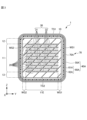
- FIG. 1 is an external perspective view of a multilayer ceramic capacitor according to a first embodiment; This is a cross-sectional view of FIG.
- FIG. 3 is a cross-sectional view taken along line III-III of FIG. 2.
- FIG. 3 is a cross-sectional view of FIG. 2 along the line IVA-IVA.
- 4 is a cross-sectional view taken along line IVB-IVB of FIG. 2.
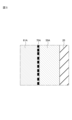
- FIG. 3 is an enlarged cross-sectional view of a portion indicated by R in FIG. 2 .
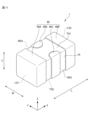
- FIG. 1 is a diagram showing a multilayer ceramic capacitor having a double structure.
- FIG. 1 is a diagram showing a multilayer ceramic capacitor having a triple structure.
- FIG. 1 is a diagram showing a multilayer ceramic capacitor having a four-row structure.
- FIG. 1 is a diagram showing a multilayer ceramic capacitor having a double structure.
- FIG. 3 is a cross-sectional view corresponding to FIG. 2 in a modified example.
- FIG. 4B is a cross-sectional view corresponding to FIG. 4A in a modified example.
- FIG. 5 is a cross-sectional view corresponding to FIG. 4B in a modified example.
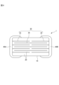
- FIG. 11 is an external perspective view of a multilayer ceramic capacitor according to a second embodiment.
- FIG. 4B is a cross-sectional view corresponding to FIG. 4A in the second embodiment.
- FIG. 5 is a cross-sectional view corresponding to FIG. 4B in the second embodiment.
- FIG. 1 is an external perspective view of the multilayer ceramic capacitor 1 according to the first embodiment.
- FIG. 2 is a cross-sectional view taken along II-II in FIG. 1.
- FIG. 3 is a cross-sectional view taken along III-III in FIG. 2.
- FIG. 4A is a cross-sectional view taken along IVA-IVA in FIG. 2.
- FIG. 4B is a cross-sectional view taken along IVB-IVB in FIG. 2.
- FIG. 5 is an enlarged cross-sectional view of a portion indicated by R in FIG. 2.
- the multilayer ceramic capacitor 1 As shown in FIG. 1, the multilayer ceramic capacitor 1 according to the first embodiment has a substantially rectangular parallelepiped shape.
- the multilayer ceramic capacitor 1 includes a laminate 10 having a substantially rectangular parallelepiped shape, and a pair of external electrodes 40 arranged at a distance from each other on both ends of the laminate 10.
- arrow T indicates the stacking direction of the multilayer ceramic capacitor 1 and the laminate 10. This stacking direction T is also the thickness direction and height direction of the multilayer ceramic capacitor 1 and the laminate 10.
- arrow L indicates the length direction of the multilayer ceramic capacitor 1 and the laminate 10, which is perpendicular to the stacking direction T.
- arrow W indicates the width direction of the multilayer ceramic capacitor 1 and the laminate 10, which is perpendicular to the stacking direction T and the length direction L.
- a pair of external electrodes 40 are respectively disposed at one end and the other end of the length direction L of the laminate 10.
- FIGS. 1 to 4B show an XYZ orthogonal coordinate system.
- the length direction L of the multilayer ceramic capacitor 1 and the laminate 10 corresponds to the X direction.
- the width direction W of the multilayer ceramic capacitor 1 and the laminate 10 corresponds to the Y direction.
- the stacking direction T of the multilayer ceramic capacitor 1 and the laminate 10 corresponds to the Z direction.
- the cross section shown in FIG. 2 is also called the LT cross section.
- the cross section shown in FIG. 3 is also called the WT cross section.
- the cross sections shown in FIG. 4A and FIG. 4B are also called the LW cross section.
- the laminate 10 includes a first main surface TS1 and a second main surface TS2 that face the stacking direction T, a first end surface LS1 and a second end surface LS2 that face the length direction L that is perpendicular to the stacking direction T, and a first side surface WS1 and a second side surface WS2 that face the width direction W that is perpendicular to the stacking direction T and the length direction L.
- the laminate 10 has a generally rectangular parallelepiped shape.
- the dimension of the laminate 10 in the length direction L is not necessarily longer than the dimension in the width direction W. It is preferable that the corners and ridges of the laminate 10 are rounded. A corner is a portion where three faces of the laminate intersect, and a ridge is a portion where two faces of the laminate intersect. Incidentally, unevenness may be formed on part or all of the surfaces constituting the laminate 10.
- the dimensions of the laminate 10 are not particularly limited, but if the dimension of the laminate 10 in the length direction L is the L dimension, it is preferable that the L dimension is 0.2 mm or more and 10 mm or less. If the dimension of the laminate 10 in the stacking direction T is the T dimension, it is preferable that the T dimension is 0.1 mm or more and 10 mm or less. If the dimension of the laminate 10 in the width direction W is the W dimension, it is preferable that the W dimension is 0.1 mm or more and 10 mm or less.
- the laminate 10 has an inner layer portion 11, and a first main surface side outer layer portion 12 and a second main surface side outer layer portion 13 arranged to sandwich the inner layer portion 11 in the stacking direction T.
- the inner layer portion 11 includes a plurality of dielectric layers 20 as a plurality of ceramic layers stacked alternately in the stacking direction T, and a plurality of internal electrode layers 30 as a plurality of internal conductor layers.
- the inner layer portion 11 includes the internal electrode layer 30 located closest to the first principal surface TS1 in the stacking direction T to the internal electrode layer 30 located closest to the second principal surface TS2.
- the multiple internal electrode layers 30 are arranged opposite each other with the dielectric layer 20 interposed therebetween.
- the inner layer portion 11 is a portion that generates electrostatic capacitance and essentially functions as a capacitor.
- the multiple dielectric layers 20 are made of a dielectric material.
- the dielectric material may be, for example, a dielectric ceramic containing components such as BaTiO3 , CaTiO3 , SrTiO3 , or CaZrO3 .
- the dielectric material may also be a material in which a subcomponent such as a Mn compound, an Fe compound, a Cr compound, a Co compound, or a Ni compound is added to the main components. It is particularly preferable that the dielectric material is a material containing BaTiO3 as the main component.
- the thickness of the dielectric layer 20 is preferably 0.5 ⁇ m or more and 15 ⁇ m or less.
- the number of dielectric layers 20 to be stacked is preferably 10 or more and 700 or less.
- the number of dielectric layers 20 is the total number of the dielectric layers 20 in the inner layer portion 11 and the number of dielectric layers 20 in each of the first main surface side outer layer portion 12 and the second main surface side outer layer portion 13.
- the multiple internal electrode layers 30 include multiple first internal electrode layers 31 as multiple first internal conductor layers, and multiple second internal electrode layers 32 as multiple second internal conductor layers.
- the first internal electrode layers 31 and the second internal electrode layers 32 are alternately arranged in the stacking direction T with the dielectric layer 20 sandwiched therebetween.
- the first internal electrode layer 31 is extended to the first end face LS1.
- the second internal electrode layer 32 is extended to the second end face LS2.
- the first internal electrode layer 31 and the second internal electrode layer 32 may be collectively referred to as the internal electrode layer 30.
- the first internal electrode layer 31 has a first opposing portion 31A and a first extension portion 31B.
- the first opposing portion 31A is a region that faces the second internal electrode layer 32 with the dielectric layer 20 sandwiched therebetween, and is located inside the laminate 10.
- the first extension portion 31B is a portion that is extended from the first opposing portion 31A to the first end face LS1, and is exposed at the first end face LS1.
- the second internal electrode layer 32 has a second opposing portion 32A and a second lead-out portion 32B.
- the second opposing portion 32A is a region facing the first internal electrode layer 31 with the dielectric layer 20 sandwiched therebetween, and is located inside the laminate 10.
- the second lead-out portion 32B is a portion that is led out from the second opposing portion 32A to the second end face LS2, and is exposed at the second end face LS2.
- the first opposing portion 31A and the second opposing portion 32A face each other via the dielectric layer 20, forming a capacitance and exhibiting the characteristics of a capacitor.
- the shapes of the first opposing portion 31A and the second opposing portion 32A are not particularly limited, but are preferably rectangular. However, the corners of the rectangular shape may be rounded or the corners of the rectangular shape may be formed at an angle.
- the shapes of the first pull-out portion 31B and the second pull-out portion 32B are not particularly limited, but are preferably rectangular. However, the corners of the rectangular shape may be rounded or the corners of the rectangular shape may be formed at an angle.
- the dimension in the width direction W of the first opposing portion 31A and the dimension in the width direction W of the first pull-out portion 31B may be the same, or one of the dimensions may be smaller.
- the dimension in the width direction W of the second opposing portion 32A and the dimension in the width direction W of the second pull-out portion 32B may be the same, or one of the dimensions may be smaller.
- the first internal electrode layer 31 and the second internal electrode layer 32 are made of an appropriate conductive material, such as a metal such as Ni, Cu, Ag, Pd, or Au, or an alloy containing at least one of these metals. When an alloy is used, the first internal electrode layer 31 and the second internal electrode layer 32 may be made of, for example, an Ag-Pd alloy.
- each of the first internal electrode layer 31 and the second internal electrode layer 32 is preferably, for example, 0.2 ⁇ m or more and 2.0 ⁇ m or less.
- the total number of the first internal electrode layers 31 and the second internal electrode layers 32 is preferably 10 or more and 700 or less.
- the first main surface side outer layer portion 12 is located on the first main surface TS1 side of the laminate 10.
- the first main surface side outer layer portion 12 is a collection of multiple dielectric layers 20 located between the first main surface TS1 and the internal electrode layer 30 closest to the first main surface TS1.
- the second main surface side outer layer portion 13 is located on the second main surface TS2 side of the laminate 10.
- the second main surface side outer layer portion 13 is a collection of multiple dielectric layers 20 located between the second main surface TS2 and the internal electrode layer 30 closest to the second main surface TS2.
- the dielectric layers 20 used in the first main surface side outer layer portion 12 and the second main surface side outer layer portion 13 may be the same as the dielectric layers 20 used in the internal layer portion 11.
- the laminate 10 has an opposing electrode portion 11E.
- the opposing electrode portion 11E is a portion where the first opposing portion 31A of the first internal electrode layer 31 and the second opposing portion 32A of the second internal electrode layer 32 face each other.
- the opposing electrode portion 11E is configured as a part of the inner layer portion 11.
- Figures 4A and 4B show the range of the width direction W and length direction L of the opposing electrode portion 11E.
- the opposing electrode portion 11E is also called the effective portion of the capacitor.
- the laminate 10 has a side surface outer layer portion.
- the side surface outer layer portion has a first side surface outer layer portion WG1 and a second side surface outer layer portion WG2.
- the first side surface outer layer portion WG1 is a portion including the dielectric layer 20 located between the opposing electrode portion 11E and the first side surface WS1.
- the second side surface outer layer portion WG2 is a portion including the dielectric layer 20 located between the opposing electrode portion 11E and the second side surface WS2.
- Figures 3, 4A, and 4B show the range of the width direction W of the first side surface outer layer portion WG1 and the second side surface outer layer portion WG2.
- the side surface outer layer portion is also called a W gap or a side gap.
- the laminate 10 has an end surface side outer layer portion.
- the end surface side outer layer portion has a first end surface side outer layer portion LG1 and a second end surface side outer layer portion LG2.
- the first end surface side outer layer portion LG1 is a portion that includes the dielectric layer 20 and the first lead portion 31B, located between the counter electrode portion 11E and the first end surface LS1.
- the first end surface side outer layer portion LG1 is an assembly of the portions of the multiple dielectric layers 20 on the first end surface LS1 side and the multiple first lead portions 31B.
- the second end surface side outer layer portion LG2 is a portion that includes the dielectric layer 20 and the second lead portion 32B, located between the counter electrode portion 11E and the second end surface LS2.
- the second end surface side outer layer portion LG2 is an assembly of the portions of the multiple dielectric layers 20 on the second end surface LS2 side and the multiple second lead portions 32B. 2, 4A, and 4B show the range of the length direction L of the first end surface side outer layer portion LG1 and the second end surface side outer layer portion LG2.
- the end surface side outer layer portion is also called the L gap or end gap.
- the external electrode 40 has a first external electrode 40A arranged on the first end face LS1 side of the laminate 10, and a second external electrode 40B arranged on the second end face LS2 side of the laminate 10.
- the first external electrode 40A and the second external electrode 40B have the same basic configuration. Furthermore, the first external electrode 40A and the second external electrode 40B have shapes that are roughly plane-symmetrical with respect to a WT cross section at the center of the longitudinal direction L of the multilayer ceramic capacitor 1. Therefore, in the following, when it is not necessary to distinguish between the first external electrode 40A and the second external electrode 40B, the first external electrode 40A and the second external electrode 40B may be collectively referred to as the external electrodes 40.
- the first external electrode 40A is disposed on the first end face LS1.
- the first external electrode 40A is in contact with the first lead portions 31B of the first internal electrode layers 31 exposed on the first end face LS1. This allows the first external electrode 40A to be electrically connected to the first internal electrode layers 31.
- the first external electrode 40A may also be disposed on a portion of the first main surface TS1 and a portion of the second main surface TS2, as well as a portion of the first side surface WS1 and a portion of the second side surface WS2.
- the first external electrode 40A is formed to extend from the first end face LS1 to a portion of the first main surface TS1 and a portion of the second main surface TS2, as well as a portion of the first side surface WS1 and a portion of the second side surface WS2.
- the second external electrode 40B is disposed on the second end face LS2.
- the second external electrode 40B is in contact with the second lead portions 32B of the second internal electrode layers 32 exposed on the second end face LS2. This allows the second external electrode 40B to be electrically connected to the second internal electrode layers 32.
- the second external electrode 40B may also be disposed on a portion of the first main surface TS1 and a portion of the second main surface TS2, as well as a portion of the first side surface WS1 and a portion of the second side surface WS2.
- the second external electrode 40B is formed to extend from the second end face LS2 to a portion of the first main surface TS1 and a portion of the second main surface TS2, as well as a portion of the first side surface WS1 and a portion of the second side surface WS2.
- the first opposing portion 31A of the first internal electrode layer 31 and the second opposing portion 32A of the second internal electrode layer 32 face each other via the dielectric layer 20, forming a capacitance. Therefore, the characteristics of a capacitor are expressed between the first external electrode 40A to which the first internal electrode layer 31 is connected and the second external electrode 40B to which the second internal electrode layer 32 is connected.
- the first external electrode 40A has a first base electrode layer 50A, a first organic layer 70A arranged on the first base electrode layer 50A, and a first plating layer 60A arranged on the first organic layer 70A.
- the second external electrode 40B has a second base electrode layer 50B, a second organic layer 70B arranged on the second base electrode layer 50B, and a second plating layer 60B arranged on the second organic layer 70B.
- the first base electrode layer 50A is disposed on the first end face LS1.
- the first base electrode layer 50A is connected to the first lead portions 31B of each of the first internal electrode layers 31 exposed at the first end face LS1.
- the first base electrode layer 50A is formed to extend from the first end face LS1 to a portion of the first main surface TS1 and a portion of the second main surface TS2, as well as a portion of the first side surface WS1 and a portion of the second side surface WS2.
- the second base electrode layer 50B is disposed on the second end face LS2.
- the second base electrode layer 50B is in contact with the second lead portions 32B of each of the multiple second internal electrode layers 32 exposed at the second end face LS2.
- the second base electrode layer 50B is formed to extend from the second end face LS2 to a portion of the first main surface TS1 and a portion of the second main surface TS2, as well as a portion of the first side surface WS1 and a portion of the second side surface WS2.
- the first base electrode layer 50A and the second base electrode layer 50B of this embodiment are baked layers.
- the baked layer preferably contains a metal component and either a glass component or a ceramic component, or both.
- the metal component includes at least one selected from, for example, Cu, Ni, Ag, Pd, Ag-Pd alloy, Au, etc.
- the glass component includes at least one selected from, for example, B, Si, Ba, Mg, Al, Li, etc.
- the ceramic component may be the same type of ceramic material as the dielectric layer 20, or a different type of ceramic material.
- the ceramic component includes at least one selected from, for example, BaTiO 3 , CaTiO 3 , (Ba, Ca)TiO 3 , SrTiO 3 , CaZrO 3 , etc.
- the main component metal of the first base electrode layer 50A and the main component metal of the second base electrode layer 50B are preferably Cu.
- the baked layer is formed by, for example, applying a conductive paste containing glass and metal to the laminate 10 and baking it.
- the baked layer can be formed by simultaneously baking the laminated chip before firing, which is the material of the laminate 10 having a plurality of internal electrodes and dielectric layers, and the conductive paste applied to the laminated chip.
- the baked layer may be formed by baking the laminate 10 after the laminated chip is fired to obtain the laminate 10 and then applying the conductive paste to the laminate 10 and baking it.
- it is preferable to form the baked layer by baking a material to which a ceramic material is added instead of a glass component. In that case, it is particularly preferable to use the same type of ceramic material as the dielectric layer 20 as the ceramic material to be added.
- the baked layer may be a multi-layered layer.
- the thickness of the first base electrode layer 50A located on the first end surface LS1 in the length direction L is preferably, for example, about 2 ⁇ m or more and 220 ⁇ m or less at the center of the stacking direction T and width direction W of the first base electrode layer 50A.
- the thickness of the second base electrode layer 50B located on the second end surface LS2 in the length direction L is preferably, for example, about 2 ⁇ m or more and 220 ⁇ m or less at the center of the stacking direction T and width direction W of the second base electrode layer 50B.
- the thickness of the first base electrode layer 50A provided on this portion, corresponding to the stacking direction T is preferably, for example, about 4 ⁇ m or more and 15 ⁇ m or less at the center of the length direction L and width direction W of the first base electrode layer 50A provided on this portion.
- the thickness of the first base electrode layer 50A provided on this portion in the width direction W is preferably, for example, about 4 ⁇ m or more and 15 ⁇ m or less at the center of the length direction L and stacking direction T of the first base electrode layer 50A provided on this portion.
- the thickness of the second base electrode layer 50B provided on this portion, corresponding to the stacking direction T is preferably, for example, about 4 ⁇ m or more and 15 ⁇ m or less at the center in the length direction L and width direction W of the second base electrode layer 50B provided on this portion.
- the thickness of the second base electrode layer 50B provided on this portion in the width direction W is preferably, for example, about 4 ⁇ m or more and 15 ⁇ m or less at the center of the length direction L and stacking direction T of the second base electrode layer 50B provided on this portion.
- the first organic layer 70A is disposed so as to cover the first base electrode layer 50A. Details of the first organic layer 70A will be described later.
- the second organic layer 70B is disposed so as to cover the second base electrode layer 50B. Details of the second organic layer 70B will be described later.
- the first plating layer 60A is disposed so as to cover the first organic layer 70A.
- the second plating layer 60B is disposed so as to cover the second organic layer 70B.
- the first plating layer 60A and the second plating layer 60B may contain, for example, at least one selected from Cu, Ni, Sn, Ag, Pd, an Ag-Pd alloy, Au, etc.
- the first plating layer 60A and the second plating layer 60B may each be formed of multiple layers.
- the first plating layer 60A and the second plating layer 60B preferably have a two-layer structure in which a Sn plating layer is formed on a Ni plating layer.
- the first plating layer 60A is disposed so as to cover the first organic layer 70A.
- the first plating layer 60A has a first Ni plating layer 61A and a first Sn plating layer 62A located on the first Ni plating layer 61A.
- the second plating layer 60B is disposed so as to cover the second organic layer 70B.
- the second plating layer 60B has a second Ni plating layer 61B and a second Sn plating layer 62B located on the second Ni plating layer 61B.
- the Ni plating layer prevents the first and second underlying electrode layers 50A and 50B from being eroded by solder when mounting the multilayer ceramic capacitor 1.
- the Sn plating layer improves the wettability of the solder when mounting the multilayer ceramic capacitor 1, thereby making it easier to mount the multilayer ceramic capacitor 1.
- the thickness of each of the first Ni plating layer 61A, the first Sn plating layer 62A, the second Ni plating layer 61B, and the second Sn plating layer 62B is preferably 2 ⁇ m or more and 15 ⁇ m or less.
- the external electrode 40 of this embodiment may have, for example, a conductive resin layer containing conductive particles and a thermosetting resin.
- the conductive resin layer may be disposed so as to cover the baked layer.
- the conductive resin layer is disposed between the baked layer and the organic layer 70 (first organic layer 70A, second organic layer 70B).
- the conductive resin layer may completely cover the baked layer, or may cover a portion of the baked layer.
- the conductive resin layer containing a thermosetting resin is more flexible than, for example, a conductive layer made of a plating film or a fired conductive paste. Therefore, even if the multilayer ceramic capacitor 1 is subjected to a physical shock or a shock caused by a thermal cycle, the conductive resin layer functions as a buffer layer. Therefore, the conductive resin layer suppresses the occurrence of cracks in the multilayer ceramic capacitor 1.
- the metal constituting the conductive particles may be Ag, Cu, Ni, Sn, Bi, or an alloy containing these.
- the conductive particles preferably contain Ag.
- the conductive particles are, for example, Ag metal powder. Ag has the lowest resistivity of all metals, making it suitable as an electrode material. In addition, Ag is a precious metal, so it is resistant to oxidation and has high weather resistance. Therefore, Ag metal powder is suitable as a conductive particle.
- the conductive particles may also be metal powder with an Ag-coated surface.
- the metal powder is preferably a powder of Cu, Ni, Sn, Bi or an alloy thereof. In order to make the base metal less expensive while maintaining the properties of Ag, it is preferable to use Ag-coated metal powder.
- the conductive particles may be Cu or Ni that has been subjected to an anti-oxidation treatment.
- the conductive particles may also be metal powder with a surface coating of Sn, Ni, or Cu.
- the metal powder is Ag, Cu, Ni, Sn, Bi, or an alloy powder of these.
- the shape of the conductive particles is not particularly limited.
- the conductive particles may be spherical, flat, or other shapes, but it is preferable to use a mixture of spherical metal powder and flat metal powder.
- the conductive particles contained in the conductive resin layer are primarily responsible for ensuring the electrical conductivity of the conductive resin layer. Specifically, when multiple conductive particles come into contact with each other, a conductive path is formed inside the conductive resin layer.
- the resin constituting the conductive resin layer may contain at least one selected from various known thermosetting resins, such as epoxy resin, phenol resin, urethane resin, silicone resin, and polyimide resin.
- thermosetting resins such as epoxy resin, phenol resin, urethane resin, silicone resin, and polyimide resin.
- epoxy resin which has excellent heat resistance, moisture resistance, and adhesion, is one of the most suitable resins.
- the resin of the conductive resin layer contains a hardener in addition to the thermosetting resin.
- the hardener of the epoxy resin may be various known compounds such as phenol-based, amine-based, acid anhydride-based, imidazole-based, active ester-based, and amide-imide-based compounds.
- the conductive resin layer may be formed of multiple layers.
- the thickness of the thickest part of the conductive resin layer is preferably 10 ⁇ m or more and 200 ⁇ m or less.
- the organic layer 70 according to this embodiment includes a first organic layer 70A and a second organic layer 70B.
- the first organic layer 70A is disposed on the first base electrode layer 50A.
- the first plating layer 60A is disposed on the first organic layer 70A.
- the first organic layer 70A may also be disposed on a part of the first main surface TS1 and a part of the second main surface TS2, and a part of the first side surface WS1 and a part of the second side surface WS2.
- the first organic layer 70A is formed to extend to approximately the center in the length direction L of the first main surface TS1 and the second main surface TS2, and to approximately the center in the length direction L of the first side surface WS1 and the second side surface WS2.
- the second organic layer 70B is disposed on the second base electrode layer 50B.
- the second plating layer 60B is disposed on the second organic layer 70B.
- the second organic layer 70B may also be disposed on a part of the first main surface TS1 and a part of the second main surface TS2, and a part of the first side surface WS1 and a part of the second side surface WS2.
- the second organic layer 70B is formed to extend to approximately the center in the length direction L of the first main surface TS1 and the second main surface TS2, and to approximately the center in the length direction L of the first side surface WS1 and the second side surface WS2.
- first organic layer 70A and the second organic layer 70B are integrally formed at approximately the center in the length direction L of the first principal surface TS1 and the second principal surface TS2, and at approximately the center in the length direction L of the first side surface WS1 and the second side surface WS2.
- first organic layer 70A and the second organic layer 70B of this embodiment are integrally formed so as to cover the entire portion of the surface of the laminate 10 that is exposed from the external electrode 40.
- FIG. Fig. 5 is an enlarged cross-sectional view of the portion indicated by R in Fig. 2.
- the state of the first base electrode layer 50A covered by the first organic layer 70A will be described, but the state of the second base electrode layer 50A covered by the second organic layer 70B is similar, so description thereof will be omitted.
- the first organic layer 70A is formed between the first base electrode layer 50A formed on the dielectric layer 20 and the first Ni plating layer 61A.
- the surface of the first organic layer 70A is formed as a surface where a part of the first base electrode layer 50A is exposed. That is, the first organic layer 70A has a plurality of voids as shown in FIG. 5.
- the atomic percentage of the main component metal of the first base electrode layer 50A is 4.0 atom % or less. It is more preferable that on the surface of the first organic layer 70A, the atomic percentage of the main component metal of the first base electrode layer 50A is 3.0 atom % or less.
- the surface of the second organic layer 70B is formed as a surface where a part of the second base electrode layer 50B is exposed. That is, the second organic layer 70B has a plurality of voids as shown in FIG. 5.
- the atomic percentage of the main component metal of the second base electrode layer 50B is 4.0 atom % or less. It is more preferable that on the surface of the second organic layer 70B, the atomic percentage of the main component metal of the second base electrode layer 50B is 3.0 atom % or less.
- the atomic percentage of the main component metal of the first base electrode layer 50A is preferably 0.6 atom% or more.
- the atomic percentage of the main component metal of the second base electrode layer 50B is preferably 0.6 atom% or more.
- the main component metal of the first base electrode layer 50A and the main component metal of the second base electrode layer 50B are preferably Cu.
- the main component metal of the first base electrode layer 50A and the main component metal of the second base electrode layer 50B are not limited to Cu.
- Ni, Ag, Pd, Ag-Pd alloy, Au, etc. may be used.
- the first organic layer 70A and the second organic layer 70B contain an organosilicon compound. This allows the first organic layer 70A and the second organic layer 70B to be reliably formed on the surfaces of the laminate 10, the base electrode layer 50, etc., improving reliability.
- the compositions constituting the first organic layer 70A and the second organic layer 70B are not limited to this.
- the first organic layer 70A and the second organic layer 70B can be, for example, a fatty acid coat.
- the fatty acid coat is a layer formed so that fatty acids are dotted on the surface of the base electrode layer.
- the fatty acid is present at least on the surface of the base electrode layer. More specifically, the fatty acid is present at least on the surface of the first base electrode layer 50A and the surface of the second base electrode layer 50B.
- the carboxyl group of the fatty acid is ionized and adsorbed to the base electrode layer by ionic bonding force, and the deposition of the plating of the plating layer provided on the base electrode layer is inhibited at the adsorption portion, and the bonding area between the base electrode layer and the plating layer can be reduced. Therefore, the adhesion between the base electrode layer and the plating layer is reduced, which has the effect of promoting peeling between the base electrode layer and the plating layer formed thereon. Therefore, when the multilayer ceramic capacitor is subjected to an impact from being dropped or a thermal cycle, it is possible to stably separate the base electrode layer from the plating layer, and it is possible to release the stress. As a result, it is possible to prevent cracks from occurring in the laminate of the multilayer ceramic capacitor.
- the total atomic percentage (atom%) of Si, C, N, and O on the surface of the first organic layer 70A is preferably 90 atom% or more.
- the total atomic percentage (atom%) of Si, C, N, and O on the surface of the second organic layer 70B is preferably 90 atom% or more.
- the thickness of the first organic layer 70A is preferably 5 nm or more and 500 nm or less. Furthermore, the thickness of the first organic layer 70A is more preferably 100 nm or more and 200 nm or less.
- the thickness of the second organic layer 70B is preferably 5 nm or more and 500 nm or less. Furthermore, the thickness of the second organic layer 70B is more preferably 100 nm or more and 200 nm or less.
- the lengthwise dimension of the multilayer ceramic capacitor 1 including the laminate 10 and the external electrodes 40 is taken as L dimension, then it is preferable that the L dimension is 0.2 mm or more and 10 mm or less. If the dimension of the multilayer ceramic capacitor 1 in the stacking direction is taken as T dimension, then it is preferable that the T dimension is 0.1 mm or more and 10 mm or less. If the widthwise dimension of the multilayer ceramic capacitor 1 is taken as W dimension, then it is preferable that the W dimension is 0.1 mm or more and 10 mm or less.
- the acceleration voltage of the thermoelectrons at this time is 15 kV.
- a qualitative analysis of all elements is performed by wide scanning, and then a quantitative analysis of all elements is performed by narrow scanning, so that the abundance ratio (atom%) of all elements on the surface on the organic layer can be calculated.
- a narrow scan spectrum is calculated for elements detected from the wide scan spectrum, and the total of the detected elements is normalized to 100 atom%, and then XPS analysis is performed.
- the abundance ratio (atom %) is an atomic percentage indicating the ratio of atoms excluding hydrogen and helium.
- the method for manufacturing the multilayer ceramic capacitor 1 of this embodiment is not limited as long as it satisfies the above-mentioned requirements.
- a suitable manufacturing method includes the following steps. Each step will be described in detail below.
- a dielectric sheet for the dielectric layer 20 and a conductive paste for the internal electrode layer 30 are prepared.
- the dielectric sheet for the dielectric layer 20 and the conductive paste for the internal electrode layer 30 both contain a binder and a solvent.
- the binder and solvent may be publicly known.
- the paste made of a conductive material is, for example, a metal powder to which an organic binder and an organic solvent have been added.
- a conductive paste for the internal electrode layer 30 is printed on the dielectric sheet by, for example, screen printing or gravure printing using a printing plate that is patterned to have the shape of the internal electrode layer 30 of this embodiment. This prepares a dielectric sheet on which the pattern of the first internal electrode layer 31 is formed, and a dielectric sheet on which the pattern of the second internal electrode layer 32 is formed.
- a portion that will become the first main surface side outer layer portion 12 on the first main surface TS1 side is formed.
- dielectric sheets on which the pattern of the first internal electrode layer 31 is printed and dielectric sheets on which the pattern of the second internal electrode layer 32 is printed are alternately stacked in sequence to form a portion that will become the inner layer portion 11.
- a predetermined number of dielectric sheets on which the pattern of the internal electrode layer 30 is not printed are stacked to form a portion that will become the second main surface side outer layer portion 13 on the second main surface TS2 side. In this way, a laminated sheet is obtained.
- the laminated sheet is pressed in the lamination direction using a means such as a hydrostatic press to produce a laminated block.
- the laminated block is cut into individual pieces of a predetermined size to obtain a number of laminated chips.
- the laminated chips may be polished by barrel polishing or the like to round off the corners and edges.
- the firing temperature at this time depends on the materials of the dielectric layer 20 and the internal electrode layer 30, but is preferably, for example, 900°C or higher and 1400°C or lower.
- the base electrode layer 50 is a baked layer.
- the baked layer can be formed by applying a conductive paste containing a glass component and a metal to the laminate 10 by a method such as dipping, and then performing a baking process.
- the temperature for the baking process at this time is preferably 700°C or higher and 900°C or lower.
- the laminated chip before firing and the conductive paste applied to the laminated chip may be fired at the same time.
- the conductive paste is applied to the laminated chip before firing, and the laminated chip and the conductive paste applied to the laminated chip are fired at the same time to form the laminate 10 with the fired layer formed.
- an organic layer that loosely coats the organic compound is formed on the base electrode layer.
- One method for forming an organic layer that loosely coats the organic compound on the base electrode layer is to dilute the organic compound with an organic solvent and spray coat it. Specifically, for example, a solution is prepared by diluting a silane coupling agent with IPA (2-propanol). The laminate with the base electrode layer formed is placed in a barrel device, and the solution is spray coated onto the laminate with the base electrode layer formed. The laminate is then removed from the barrel device, spread on filter paper, and heat-treated in an oven at 100°C to 200°C for a specified time (30 to 60 minutes) to harden the organic layer.
- the organic compound can be diluted with an organic solvent to prepare a solution, and then the solution can be applied to a laminate on which a base electrode layer has been formed, followed by thermal curing to form the layer.
- the solution can be applied by dipping or the like.
- the target atomic percentage of the main component metal of the base electrode layer on the surface of the organic layer and the thickness of the organic layer can be controlled by controlling the solution concentration, application method, application time, and application temperature.
- a plating layer is formed on the surface of the organic layer 70.
- a first plating layer 60A is formed on the surface of the first organic layer 70A.
- a second plating layer 60B is formed on the surface of the second organic layer 70B.
- a Ni plating layer and a Sn plating layer are formed as the plating layers. Either electrolytic plating or electroless plating may be used for plating. However, electroless plating has the disadvantage of complicating the process because pretreatment with a catalyst or the like is required to improve the plating deposition rate. Therefore, it is usually preferable to use electrolytic plating.
- the Ni plating layer and the Sn plating layer are formed sequentially, for example, by barrel plating.
- the conductive resin layer may be disposed so as to cover the baked layer.
- a conductive resin paste containing a thermosetting resin and a metal component is applied onto the baked layer, and then heat-treated at a temperature of 250 to 550°C or higher.
- the thermosetting resin is thermally cured to form a conductive resin layer.
- the atmosphere during this heat treatment is preferably an N2 atmosphere.
- the oxygen concentration is preferably 100 ppm or less.
- the multilayer ceramic capacitor 1 is manufactured through the above manufacturing process.
- the configuration of the multilayer ceramic capacitor 1 is not limited to the configuration shown in Figures 1 to 4B.
- the multilayer ceramic capacitor 1 may be a multilayer ceramic capacitor with a double structure, triple structure, or quadruple structure as shown in Figures 6 to 8.
- the multilayer ceramic capacitor 1 shown in FIG. 6 is a multilayer ceramic capacitor 1 with a double structure, and includes, as the internal electrode layer 30, a first internal electrode layer 33 and a second internal electrode layer 34, as well as a floating internal electrode layer 35 that is not drawn out to either the first end surface LS1 or the second end surface LS2.
- the multilayer ceramic capacitor 1 shown in FIG. 7 is a multilayer ceramic capacitor 1 with a triple structure, including a first floating internal electrode layer 35A and a second floating internal electrode layer 35B as the floating internal electrode layer 35.
- the multilayer ceramic capacitor 1 with a quadruple structure, including a first floating internal electrode layer 35A, a second floating internal electrode layer 35B, and a third floating internal electrode layer 35C as the floating internal electrode layer 35.
- the multilayer ceramic capacitor 1 has a structure in which the opposing electrode portion is divided into multiple parts.
- multiple capacitor components are formed between the opposing internal electrode layers 30, and these capacitor components are connected in series.
- the voltage applied to each capacitor component is reduced, and the multilayer ceramic capacitor 1 can withstand high voltage.
- the multilayer ceramic capacitor 1 of this embodiment may have a multi-row structure of four or more rows.
- the first organic layer 70A and the second organic layer 70B extend to approximately the center in the length direction L of the first main surface TS1 and the second main surface TS2 and to approximately the center in the length direction L of the first side surface WS1 and the second side surface WS2, and are integrally formed so as to cover the entire portion of the surface of the laminate 10 that is exposed from the external electrode 40.
- the configuration of the first organic layer 70A and the second organic layer 70B is not limited to this.
- Figure 9 is a cross-sectional view of the modified example corresponding to Figure 2.
- Figure 10A is a cross-sectional view of the modified example corresponding to Figure 4A.
- Figure 10B is a cross-sectional view of the modified example corresponding to Figure 4B. Note that configurations similar to those in the first embodiment may be given the same names and detailed descriptions may be omitted.
- the multilayer ceramic capacitor 1 As shown in FIG. 1, the multilayer ceramic capacitor 1 according to the modified example has a substantially rectangular parallelepiped shape.
- the multilayer ceramic capacitor 1 includes a laminate 10 having a substantially rectangular parallelepiped shape, and a pair of external electrodes 40 arranged at a distance from each other on both ends of the laminate 10.
- the external electrode 40 has a first external electrode 40A arranged on the first end face LS1 side of the laminate 10, and a second external electrode 40B arranged on the second end face LS2 side of the laminate 10.
- the first external electrode 40A has a first base electrode layer 50A, a first organic layer 70bA arranged on the first base electrode layer 50A, and a first plating layer 60A arranged on the first organic layer 70bA.
- the second external electrode 40B has a second base electrode layer 50B, a second organic layer 70bB arranged on the second base electrode layer 50B, and a second plating layer 60B arranged on the second organic layer 70bB.
- the organic layer 70b in this modified example includes a first organic layer 70bA and a second organic layer 70bB.
- the first organic layer 70bA is disposed on the first base electrode layer 50A.
- the first plating layer 60A is disposed on the first organic layer 70bA.
- the first organic layer 70bA may also be disposed on a portion of the first principal surface TS1 and a portion of the second principal surface TS2, as well as a portion of the first side surface WS1 and a portion of the second side surface WS2.
- the first organic layer 70bA is formed to extend to a portion of the first principal surface TS1 and a portion of the second principal surface TS2, as well as a portion of the first side surface WS1 and a portion of the second side surface WS2.
- the second organic layer 70bB is disposed on the second base electrode layer 50B.
- the second plating layer 60B is disposed on the second organic layer 70bB.
- the second organic layer 70bB may also be disposed on a portion of the first principal surface TS1 and a portion of the second principal surface TS2, as well as a portion of the first side surface WS1 and a portion of the second side surface WS2.
- the second organic layer 70bB is formed to extend to a portion of the first principal surface TS1 and a portion of the second principal surface TS2, as well as a portion of the first side surface WS1 and a portion of the second side surface WS2.
- the multilayer ceramic capacitor 1 there is a portion between the first external electrode 40A and the second external electrode 40B where the organic layer 70b is not present. Therefore, the first organic layer 70bA and the second organic layer 70bB in this modified example are not formed integrally, and part of the surface of the laminate 10 is exposed. Even in this case, the organic layer is formed at the end of the base electrode layer of the external electrode, which is the starting point of the crack, so that the effect of suppressing cracks can be obtained.
- the multilayer ceramic capacitor 1 according to the first embodiment is a two-terminal type having two external electrodes, but is not limited to this and may be a multi-terminal type having a large number of external electrodes.
- Figure 11 is an external perspective view of the multilayer ceramic capacitor according to the second embodiment.
- Figure 12 is a cross-sectional view corresponding to Figure 4A in the second embodiment.
- Figure 13 is a cross-sectional view corresponding to Figure 4B in the second embodiment.
- the multilayer ceramic capacitor 1 of this embodiment differs from the first embodiment in the configuration of the internal electrode layers inside the laminate 10 and the external electrode 40.
- the multiple internal electrode layers as multiple internal conductor layers include multiple first internal electrode layers 131 as multiple first internal conductor layers that are extended to the first end face LS1 and the second end face LS2, and multiple second internal electrode layers 132 as multiple second internal conductor layers that are extended to at least one of the first side face WS1 or the second side face WS2.
- the multiple internal electrode layers include multiple first internal electrode layers 131 that are extended to the first end face LS1 and the second end face LS2, and multiple second internal electrode layers 132 that are extended to the first side face WS1 and the second side face WS2.
- the multiple first internal electrode layers 131 are arranged on the multiple dielectric layers 20.
- the multiple second internal electrode layers 132 are arranged on the multiple dielectric layers 20.
- the multiple first internal electrode layers 131 and the multiple second internal electrode layers 132 are arranged alternately in the stacking direction T of the laminate 10, with the dielectric layers 20 interposed between them.
- the first internal electrode layers 131 and the second internal electrode layers 132 are arranged so as to sandwich the dielectric layers 20 between them.
- the first internal electrode layer 131 is disposed on the dielectric layer 20 and extends from the first end face LS1 to the second end face LS2 so as to be exposed at the first end face LS1 and the second end face LS2. More specifically, the first internal electrode layer 131 has a first opposing portion 131A facing the second internal electrode layer 132, a first lead-out portion 131B extending from the first opposing portion 131A to the first end face LS1, and a second lead-out portion 131C extending from the first opposing portion 131A to the second end face LS2.
- the first opposing portion 131A is located in the center on the dielectric layer 20.
- the first lead-out portion 131B is exposed at the first end face LS1.
- the second lead-out portion 131C is exposed at the second end face LS2.
- the first internal electrode layer 131 is not exposed to the first side surface WS1 and the second side surface WS2.
- the shapes of the first opposing portion 131A of the first internal electrode layer 131, the first lead portion 131B, and the second lead portion 131C are not particularly limited.
- the second internal electrode layer 132 is disposed on the dielectric layer 20 and is disposed so as to be exposed to the first side surface WS1 and the second side surface WS2 without being exposed to the first end surface LS1 and the second end surface LS2. Specifically, the second internal electrode layer 132 extends between the first side surface WS1 and the second side surface WS2. More specifically, the second internal electrode layer 132 has a second opposing portion 132A facing the first internal electrode layer 131, a third lead portion 132B extending from the second opposing portion 132A to the first side surface WS1, and a fourth lead portion 132C extending from the second opposing portion 132A to the second side surface WS2. The second opposing portion 132A is located in the center on the dielectric layer 20.
- the second opposing portion 132A is formed in a rectangular shape so as to extend in the direction of the first end face LS1 and the direction of the second end face LS2.
- the third lead portion 132B is exposed to the first side face WS1.
- the fourth lead portion 132C is exposed to the second side face WS2.
- the second internal electrode layer 132 is not exposed to the first end face LS1 or the second end face LS2.
- the shapes of the second opposing portion 132A, the third lead portion 132B, and the fourth lead portion 132C of the second internal electrode layer 132 are not particularly limited.
- the first opposing portion 131A and the second opposing portion 132A face each other via the dielectric layer 20, forming a capacitance and exhibiting the characteristics of a capacitor.
- the external electrode 40 has at least a first external electrode 40A, a second external electrode 40B, and a third external electrode 40C.
- the external electrode 40 has a first external electrode 40A, a second external electrode 40B, a third external electrode 40C, and further a fourth external electrode 40D.
- the first external electrode 40A is disposed on the first end face LS1 and is connected to the first internal electrode layer 131.
- the first external electrode 40A is connected to the first internal electrode layer 131 that is extended to the first end face LS1. More specifically, the first external electrode 40A is connected to the first extended portion 131B of the first internal electrode layer 131.
- the first external electrode 40A is formed to extend from the first end face LS1 to a portion of the first main surface TS1 and a portion of the second main surface TS2, as well as a portion of the first side surface WS1 and a portion of the second side surface WS2.
- the second external electrode 40B is disposed on the second end face LS2 and is connected to the first internal electrode layer 131.
- the second external electrode 40B is connected to the first internal conductor layer 131 that is extended to the second end face LS2. More specifically, the second external electrode 40B is connected to the second extended portion 131C of the first internal electrode layer 131.
- the second external electrode 40B is formed extending from the second end face LS2 to a portion of the first main surface TS1 and a portion of the second main surface TS2, as well as a portion of the first side surface WS1 and a portion of the second side surface WS2.
- the third external electrode 40C is disposed on the first side surface WS1 and is connected to the second internal electrode layer 132. More specifically, the third external electrode 40C is connected to the third lead portion 132B of the second internal electrode layer 132. In this embodiment, the third external electrode 40C is disposed so as to extend from the first side surface WS1 to a portion of the first main surface TS1 and a portion of the second main surface TS2.
- the fourth external electrode 40D is disposed on the second side surface WS2 and is connected to the second internal electrode layer 132. More specifically, the fourth external electrode 40D is connected to the fourth lead portion 132C of the second internal electrode layer 132. In this embodiment, the fourth external electrode 40D is disposed so as to extend from the second side surface WS2 to a portion of the first main surface TS1 and a portion of the second main surface TS2.
- the layer structure of the external electrode 40 of this embodiment can be, for example, any of the layer structures similar to those of the external electrode 40 of the first embodiment.
- the first external electrode 40A may include a first base electrode layer 50A, a first plating layer 60A, and a first organic layer 70A
- the first plating layer 60A may include a first Ni plating layer 61A and a first Sn plating layer 62A
- the second external electrode 40B may include a second base electrode layer 50B, a second plating layer 60B, and a second organic layer 70B
- the second plating layer 60B may include a second Ni plating layer 61B and a second Sn plating layer 62B.
- the third external electrode 40C may include a third base electrode layer 50C, a third plating layer 60C, and a third organic layer 70C, and the third plating layer 60C may include a third Ni plating layer 61C and a third Sn plating layer 62C.
- the fourth external electrode 40D may include a fourth base electrode layer 50D, a fourth plating layer 60D, and a fourth organic layer 70D, and the fourth plating layer 60D may include a fourth Ni plating layer 61D and a fourth Sn plating layer 62D.
- the first base electrode layer 50A, the second base electrode layer 50B, the third base electrode layer 50C, and the fourth base electrode layer 50D may be, for example, baked layers.
- the organic layer 70 includes a first organic layer 70A, a second organic layer 70B, a third organic layer 70C, and a fourth organic layer 70D.
- the first organic layer 70A is disposed on the first base electrode layer 50A.
- the first plating layer 60A is disposed on the first organic layer 70A.
- the first organic layer 70A may also be disposed on a part of the first principal surface TS1 and a part of the second principal surface TS2, as well as a part of the first side surface WS1 and a part of the second side surface WS2, between the first external electrode 40A and the second external electrode 40B, the third external electrode 40C, and the fourth external electrode 40D in the longitudinal direction L.
- the second organic layer 70B is disposed on the second base electrode layer 50B.
- a second plating layer 60B is disposed on the second organic layer 70B.
- the second organic layer 70B may also be disposed on a part of the first principal surface TS1 and a part of the second principal surface TS2, as well as a part of the first side surface WS1 and a part of the second side surface WS2, between the second external electrode 40B and the first external electrode 40A, the third external electrode 40C, and the fourth external electrode 40D in the longitudinal direction L.
- the third organic layer 70C is disposed on the third base electrode layer 50C.
- a third plating layer 60C is disposed on the third organic layer 70C.
- the third organic layer 70C may also be disposed on a portion of the first side surface WS1 between the third external electrode 40C and the first external electrode 40A in the length direction L, and between the third external electrode 40C and the second external electrode 40B in the length direction L.
- the third organic layer 70C may also be disposed on a portion of the first main surface TS1 and a portion of the second main surface TS2.
- the fourth organic layer 70D is disposed on the fourth base electrode layer 50D.
- a fourth plating layer 60D is disposed on the fourth organic layer 70D.
- the fourth organic layer 70D may also be disposed on a portion of the second side surface WS2 between the fourth external electrode 40D and the first external electrode 40A in the length direction L, and between the fourth external electrode 40D and the second external electrode 40B in the length direction L.
- the fourth organic layer 70D may also be disposed on a portion of the first main surface TS1 and a portion of the second main surface TS2.
- the first organic layer 70A, the second organic layer 70B, the third organic layer 70C, and the fourth organic layer 70D are integrally formed so as to cover the entire portion of the surface of the laminate 10 that is exposed from the external electrodes 40.
- the organic layers are formed at the ends of the base electrode layers of the external electrodes, which are the starting points of cracks, so that the effect of suppressing cracks can be obtained.
- the organic layers include at least the first organic layer 70A and the second organic layer 70B.
- a multilayer ceramic capacitor in which a dielectric layer 20 made of a dielectric ceramic is used as a ceramic layer is exemplified as a multilayer ceramic electronic component.
- the multilayer ceramic electronic components of the present disclosure are not limited to this.
- the ceramic electronic components of the present disclosure can also be applied to various multilayer ceramic electronic components such as piezoelectric components using piezoelectric ceramic as a ceramic layer, and thermistors using semiconductor ceramic as a ceramic layer.
- piezoelectric ceramics include PZT (lead zirconate titanate) ceramics
- semiconductor ceramics include spinel ceramics.
- the multilayer ceramic capacitor 1 according to the embodiment described above provides the following advantages:
- the multilayer ceramic capacitor 1 includes a laminate 10 including a plurality of dielectric layers 20 (ceramic layers 20) and a plurality of internal electrode layers 30 (internal conductor layers 30) that are alternately stacked, and has a first main surface TS1 and a second main surface TS2 that face a height direction T, a first side surface WS1 and a second side surface WS2 that face a width direction W that is perpendicular to the height direction T, and a first end surface LS1 and a second end surface LS2 that face a length direction L that is perpendicular to the height direction T and the width direction W, and an external electrode 40 connected to the internal electrode layer 30, the external electrode 40 having a first external electrode 40A arranged on the first end surface LS1 and a second external electrode 40B arranged on the second end surface LS2, the first external electrode 40A having a first base electrode layer 50A arranged on the first end surface LS1 and a first base electrode layer 50B arranged on the first end
- the second external electrode 40B has a first organic layer 70A disposed on the second end face LS1, and a first plating layer 60A disposed on the first organic layer 70A, and the second external electrode 40B has a second base electrode layer 50B disposed on the second base electrode layer 50B, and a second plating layer 60B disposed on the second organic layer 70B, and the surface of the first organic layer 70A is
- the surface of the second organic layer 70B is formed as a surface on which a portion of the second base electrode layer 50B is exposed, and the atomic percentage of the main component metal of the first base electrode layer 50A on the surface of the first organic layer 70A is 4.0 atom % or less, and the atomic percentage of the main component metal of the second base electrode layer 50B on the surface of the second organic layer 70B is 4.0 atom % or less.
- the atomic percentage of the main component metal of the first base electrode layer 50A on the surface of the first organic layer 70A is 0.6 atom % or more
- the atomic percentage of the main component metal of the second base electrode layer 50B on the surface of the second organic layer 70B is 0.6 atom % or more.
- the main component metal of the first base electrode layer 50A and the main component metal of the second base electrode layer 50B are Cu.
- the first organic layer 70A and the second organic layer 70B are organosilicon compounds.
- the multilayer ceramic capacitor 1 has a plurality of internal electrode layers 30 including a plurality of first internal electrode layers 31 extending to the first end face LS1 and a plurality of second internal electrode layers 32 extending to the second end face LS2, with the first external electrode 40A connected to the first internal electrode layer 31 and the second external electrode 40B connected to the second internal electrode layer 32.
- the external electrode 40 further includes a third external electrode 40C (or a fourth external electrode 40D), and the multiple internal electrode layers 30 include multiple first internal electrode layers 131 extended to the first end face LS1 and the second end face LS2, and multiple second internal electrode layers 132 extended to at least one of the first side face WS1 or the second side face WS2, and the first external electrode 40A is connected to the first internal electrode layer 131 extended to the first end face LS1, the second external electrode 40B is connected to the first internal electrode layer 131 extended to the second end face LS2, and the third external electrode 40C (or the fourth external electrode 40D) is connected to the second internal electrode layer 132.
- the third external electrode 40C or the fourth external electrode 40D
- the present invention is not limited to the configurations of the above embodiments, and can be modified as appropriate within the scope of the present invention without changing the gist of the invention. Note that the present invention also includes a combination of two or more of the individual desirable configurations described in the above embodiments.
- multilayer ceramic capacitors having the structures shown in Figures 1 to 5 were fabricated as samples for the examples and comparative examples. Specifically, multiple lots of multilayer ceramic capacitors fabricated so that the atomic percentage of the main component metal of the base electrode layer on the surface of the organic layer was different were fabricated as samples for Examples 1 to 7 and Comparative Examples 1 to 5.
- Samples from the same lot were produced under the same manufacturing conditions, and the external electrodes had the same specifications.
- 110 samples were produced for each lot (Examples 1-7 and Comparative Examples 1-5). Of the 110 samples produced for each lot, 100 samples were checked for the presence or absence of plating defects, and then a deflection strength test was performed. The atomic percentage of the main component metal of the base electrode layer on the surface of the organic layer was measured using the remaining 10 samples produced in the same lot. The atomic percentage of the main component metal of the base electrode layer on the surface of the organic layer was measured using the measurement method described above, and the average value of the 10 samples was used as the measurement result.
- Plating layer Formed in two layers, with a Ni plating layer formed on the base electrode layer on which the fatty acid was arranged, and a Sn plating layer formed on the Ni plating layer.
- the multilayer ceramic capacitor was mounted on a mounting board with a thickness of 1.6 mm using solder paste. After that, the board was bent from the back side of the board where the multilayer ceramic capacitor was not mounted using a push rod with a curvature radius of 1 ⁇ m to apply mechanical stress. At this time, the deflection amount was set to 2 mm, and the board was bent for 60 seconds. Note that the conditions for this test were stricter than the AEC-Q200 standard required for electronic components for automotive use.
- the multilayer ceramic capacitor was removed from the board, the cross section was polished, and the presence or absence of cracks in the laminate was observed.
- the cross section was polished so that the LT surface of the multilayer ceramic capacitor was exposed up to a position that was 1/2 of the width direction W connecting the first end face and the second end face of the multilayer ceramic capacitor.
- Table 1 shows the results of measuring the atomic percentage of the main component metal of the base electrode layer on the surface of the organic layer, Cu (atom %), and the evaluation results of the number of cracks generated in the bending strength test and the number of plating defects generated, for the samples of Examples 1 to 7 and Comparative Examples 1 to 5.
- the atomic percentage of the main component metal of the base electrode layer on the surface of the organic layer is 3.0 atom% or less.
- Comparative Example 1 which is a sample in which the surface of the organic layer is not formed as a surface on which a part of the base electrode layer is exposed, the atomic percentage of the main component metal of the base electrode layer on the surface of the organic layer was 0.0 atom%, and plating defects occurred. It is preferable that the surface of the organic layer is formed as a surface on which a part of the base electrode layer is exposed, and it is more preferable that the atomic percentage of the main component metal of the base electrode layer on the surface of the organic layer is 0.6 atom% or more. This can also suppress the occurrence of plating defects.
- the atomic percentage of the main component metal of the base electrode layer on the surface of the organic layer is 0.6 atom% or more and 4.0 atom% or less. It is also more preferable that the atomic percentage of the main component metal of the base electrode layer on the surface of the organic layer is 0.6 atom% or more and 3.0 atom% or less.
- a laminate including a plurality of ceramic layers and a plurality of internal conductor layers stacked alternately, the laminate having a first main surface and a second main surface opposed to each other in a height direction, a first side surface and a second side surface opposed to each other in a width direction perpendicular to the height direction, and a first end surface and a second end surface opposed to each other in a length direction perpendicular to the height direction and the width direction; an external electrode connected to the internal conductor layer; the external electrodes include a first external electrode disposed on the first end surface and a second external electrode disposed on the second end surface; the first external electrode has a first base electrode layer disposed on the first end face, a first organic layer disposed on the first base electrode layer, and a first plating layer disposed on the first organic layer; the second external electrode has a second base electrode layer disposed on the second end face, a second organic layer disposed on the second base electrode layer, and a second plating layer disposed on the second organic layer,
- the plurality of internal conductor layers include a plurality of first internal conductor layers extended to the first end surface and a plurality of second internal conductor layers extended to the second end surface; the first external electrode is connected to the first internal conductor layer;
- the multilayer ceramic electronic component according to any one of ⁇ 1> to ⁇ 4>, wherein the second external electrodes are connected to the second internal conductor layers.
- the external electrodes further include a third external electrode
- the plurality of internal conductor layers include a plurality of first internal conductor layers extending to the first end face and the second end face, and a plurality of second internal conductor layers extending to at least one of the first side face and the second side face;
- the first external electrode is connected to the first internal conductor layer that is extended to the first end face;
- the second external electrode is connected to the first internal conductor layer that is extended to the second end face,
- the multilayer ceramic electronic component according to any one of ⁇ 1> to ⁇ 4>, wherein the third external electrode is connected to the second internal conductor layer.
- Multilayer ceramic capacitors multilayer ceramic electronic components
- Laminate 20 Dielectric layer (ceramic layer) 30 Internal electrode layer (internal conductor layer) 40 External electrode 40A First external electrode 40B Second external electrode 50A First base electrode layer 50B Second base electrode layer 60A First plating layer 60B Second plating layer 70A First organic layer 70B Second organic layer L Length direction LS1 First end face LS2 Second end face T Height direction TS1 First main surface TS2 Second main surface W Width direction WS1 First side surface WS2 Second side surface
Landscapes
- Engineering & Computer Science (AREA)
- Power Engineering (AREA)
- Manufacturing & Machinery (AREA)
- Microelectronics & Electronic Packaging (AREA)
- Chemical & Material Sciences (AREA)
- Ceramic Engineering (AREA)
- Inorganic Chemistry (AREA)
- Materials Engineering (AREA)
- Fixed Capacitors And Capacitor Manufacturing Machines (AREA)
- Ceramic Capacitors (AREA)
Priority Applications (5)
| Application Number | Priority Date | Filing Date | Title |
|---|---|---|---|
| JP2024565712A JPWO2024135256A1 (https=) | 2022-12-19 | 2023-11-28 | |
| EP23906624.4A EP4621819A1 (en) | 2022-12-19 | 2023-11-28 | Layered ceramic electronic component |
| CN202380086505.1A CN120359585A (zh) | 2022-12-19 | 2023-11-28 | 层叠陶瓷电子部件 |
| KR1020257012572A KR20250073228A (ko) | 2022-12-19 | 2023-11-28 | 적층 세라믹 전자부품 |
| US19/236,252 US20250308798A1 (en) | 2022-12-19 | 2025-06-12 | Multilayer ceramic electronic component |
Applications Claiming Priority (2)
| Application Number | Priority Date | Filing Date | Title |
|---|---|---|---|
| JP2022202676 | 2022-12-19 | ||
| JP2022-202676 | 2022-12-19 |
Related Child Applications (1)
| Application Number | Title | Priority Date | Filing Date |
|---|---|---|---|
| US19/236,252 Continuation US20250308798A1 (en) | 2022-12-19 | 2025-06-12 | Multilayer ceramic electronic component |
Publications (1)
| Publication Number | Publication Date |
|---|---|
| WO2024135256A1 true WO2024135256A1 (ja) | 2024-06-27 |
Family
ID=91588320
Family Applications (1)
| Application Number | Title | Priority Date | Filing Date |
|---|---|---|---|
| PCT/JP2023/042616 Ceased WO2024135256A1 (ja) | 2022-12-19 | 2023-11-28 | 積層セラミック電子部品 |
Country Status (6)
| Country | Link |
|---|---|
| US (1) | US20250308798A1 (https=) |
| EP (1) | EP4621819A1 (https=) |
| JP (1) | JPWO2024135256A1 (https=) |
| KR (1) | KR20250073228A (https=) |
| CN (1) | CN120359585A (https=) |
| WO (1) | WO2024135256A1 (https=) |
Cited By (1)
| Publication number | Priority date | Publication date | Assignee | Title |
|---|---|---|---|---|
| WO2026054040A1 (ja) * | 2024-09-06 | 2026-03-12 | 株式会社村田製作所 | 積層セラミックコンデンサ |
Citations (4)
| Publication number | Priority date | Publication date | Assignee | Title |
|---|---|---|---|---|
| JPH053132A (ja) | 1991-06-25 | 1993-01-08 | Mitsubishi Materials Corp | チツプ型積層セラミツクスコンデンサ |
| JP2020102563A (ja) * | 2018-12-25 | 2020-07-02 | 株式会社村田製作所 | 積層セラミック電子部品およびその実装構造 |
| JP2021048387A (ja) * | 2019-09-18 | 2021-03-25 | サムソン エレクトロ−メカニックス カンパニーリミテッド. | 積層型電子部品 |
| JP2022174958A (ja) * | 2021-05-12 | 2022-11-25 | 株式会社村田製作所 | 積層セラミック電子部品 |
-
2023
- 2023-11-28 CN CN202380086505.1A patent/CN120359585A/zh active Pending
- 2023-11-28 WO PCT/JP2023/042616 patent/WO2024135256A1/ja not_active Ceased
- 2023-11-28 JP JP2024565712A patent/JPWO2024135256A1/ja active Pending
- 2023-11-28 KR KR1020257012572A patent/KR20250073228A/ko active Pending
- 2023-11-28 EP EP23906624.4A patent/EP4621819A1/en active Pending
-
2025
- 2025-06-12 US US19/236,252 patent/US20250308798A1/en active Pending
Patent Citations (4)
| Publication number | Priority date | Publication date | Assignee | Title |
|---|---|---|---|---|
| JPH053132A (ja) | 1991-06-25 | 1993-01-08 | Mitsubishi Materials Corp | チツプ型積層セラミツクスコンデンサ |
| JP2020102563A (ja) * | 2018-12-25 | 2020-07-02 | 株式会社村田製作所 | 積層セラミック電子部品およびその実装構造 |
| JP2021048387A (ja) * | 2019-09-18 | 2021-03-25 | サムソン エレクトロ−メカニックス カンパニーリミテッド. | 積層型電子部品 |
| JP2022174958A (ja) * | 2021-05-12 | 2022-11-25 | 株式会社村田製作所 | 積層セラミック電子部品 |
Non-Patent Citations (1)
| Title |
|---|
| See also references of EP4621819A1 |
Cited By (1)
| Publication number | Priority date | Publication date | Assignee | Title |
|---|---|---|---|---|
| WO2026054040A1 (ja) * | 2024-09-06 | 2026-03-12 | 株式会社村田製作所 | 積層セラミックコンデンサ |
Also Published As
| Publication number | Publication date |
|---|---|
| US20250308798A1 (en) | 2025-10-02 |
| JPWO2024135256A1 (https=) | 2024-06-27 |
| EP4621819A1 (en) | 2025-09-24 |
| KR20250073228A (ko) | 2025-05-27 |
| CN120359585A (zh) | 2025-07-22 |
Similar Documents
| Publication | Publication Date | Title |
|---|---|---|
| US10840021B2 (en) | Multilayer ceramic electronic component | |
| US10453612B2 (en) | Multilayer ceramic capacitor | |
| US11062848B2 (en) | Multilayer ceramic electronic component | |
| CN115483030B (zh) | 层叠陶瓷电子部件 | |
| US11735366B2 (en) | Multilayer ceramic electronic component and method for manufacturing the same | |
| JP7517260B2 (ja) | 積層セラミック電子部品 | |
| JP7468498B2 (ja) | 積層セラミックコンデンサ | |
| JP2019192862A (ja) | 積層セラミックコンデンサおよびその製造方法 | |
| WO2023095620A1 (ja) | 積層セラミック電子部品 | |
| JP2026069621A (ja) | 積層セラミックコンデンサ | |
| JP2026069620A (ja) | 積層セラミックコンデンサ | |
| JP7501564B2 (ja) | 積層セラミック電子部品 | |
| US20250308798A1 (en) | Multilayer ceramic electronic component | |
| JP7740567B2 (ja) | 積層セラミック電子部品 | |
| JP7776002B2 (ja) | 積層セラミックコンデンサ | |
| WO2025126319A1 (ja) | 積層セラミック電子部品 | |
| US20260094766A1 (en) | Multilayer ceramic capacitor | |
| WO2024257211A1 (ja) | 積層セラミックコンデンサ | |
| CN120727458A (zh) | 层叠陶瓷电子部件 | |
| JP2026050185A (ja) | 積層セラミックコンデンサ | |
| KR20250144885A (ko) | 적층 세라믹 전자부품 | |
| WO2025094421A1 (ja) | 積層セラミック電子部品及び積層セラミック電子部品の製造方法 | |
| WO2026034048A1 (ja) | 積層セラミック電子部品 | |
| WO2025004487A1 (ja) | 積層セラミックコンデンサ |
Legal Events
| Date | Code | Title | Description |
|---|---|---|---|
| 121 | Ep: the epo has been informed by wipo that ep was designated in this application |
Ref document number: 23906624 Country of ref document: EP Kind code of ref document: A1 |
|
| ENP | Entry into the national phase |
Ref document number: 20257012572 Country of ref document: KR Kind code of ref document: A |
|
| WWE | Wipo information: entry into national phase |
Ref document number: 1020257012572 Country of ref document: KR |
|
| WWE | Wipo information: entry into national phase |
Ref document number: 2024565712 Country of ref document: JP |
|
| WWE | Wipo information: entry into national phase |
Ref document number: 202517056717 Country of ref document: IN |
|
| WWE | Wipo information: entry into national phase |
Ref document number: 2023906624 Country of ref document: EP Ref document number: 202380086505.1 Country of ref document: CN |
|
| ENP | Entry into the national phase |
Ref document number: 2023906624 Country of ref document: EP Effective date: 20250616 |
|
| WWP | Wipo information: published in national office |
Ref document number: 202517056717 Country of ref document: IN |
|
| NENP | Non-entry into the national phase |
Ref country code: DE |
|
| WWP | Wipo information: published in national office |
Ref document number: 202380086505.1 Country of ref document: CN |
|
| WWP | Wipo information: published in national office |
Ref document number: 2023906624 Country of ref document: EP |