WO2024128039A1 - Rfidタグ - Google Patents
Rfidタグ Download PDFInfo
- Publication number
- WO2024128039A1 WO2024128039A1 PCT/JP2023/043158 JP2023043158W WO2024128039A1 WO 2024128039 A1 WO2024128039 A1 WO 2024128039A1 JP 2023043158 W JP2023043158 W JP 2023043158W WO 2024128039 A1 WO2024128039 A1 WO 2024128039A1
- Authority
- WO
- WIPO (PCT)
- Prior art keywords
- conductor
- substrate
- rfid tag
- land
- rfic chip
- Prior art date
- Legal status (The legal status is an assumption and is not a legal conclusion. Google has not performed a legal analysis and makes no representation as to the accuracy of the status listed.)
- Ceased
Links
Images


Classifications
-
- G—PHYSICS
- G06—COMPUTING OR CALCULATING; COUNTING
- G06K—GRAPHICAL DATA READING; PRESENTATION OF DATA; RECORD CARRIERS; HANDLING RECORD CARRIERS
- G06K19/00—Record carriers for use with machines and with at least a part designed to carry digital markings
- G06K19/06—Record carriers for use with machines and with at least a part designed to carry digital markings characterised by the kind of the digital marking, e.g. shape, nature, code
- G06K19/067—Record carriers with conductive marks, printed circuits or semiconductor circuit elements, e.g. credit or identity cards also with resonating or responding marks without active components
- G06K19/07—Record carriers with conductive marks, printed circuits or semiconductor circuit elements, e.g. credit or identity cards also with resonating or responding marks without active components with integrated circuit chips
- G06K19/0723—Record carriers with conductive marks, printed circuits or semiconductor circuit elements, e.g. credit or identity cards also with resonating or responding marks without active components with integrated circuit chips the record carrier comprising an arrangement for non-contact communication, e.g. wireless communication circuits on transponder cards, non-contact smart cards or RFIDs
-
- G—PHYSICS
- G06—COMPUTING OR CALCULATING; COUNTING
- G06K—GRAPHICAL DATA READING; PRESENTATION OF DATA; RECORD CARRIERS; HANDLING RECORD CARRIERS
- G06K19/00—Record carriers for use with machines and with at least a part designed to carry digital markings
- G06K19/06—Record carriers for use with machines and with at least a part designed to carry digital markings characterised by the kind of the digital marking, e.g. shape, nature, code
- G06K19/067—Record carriers with conductive marks, printed circuits or semiconductor circuit elements, e.g. credit or identity cards also with resonating or responding marks without active components
- G06K19/07—Record carriers with conductive marks, printed circuits or semiconductor circuit elements, e.g. credit or identity cards also with resonating or responding marks without active components with integrated circuit chips
- G06K19/077—Constructional details, e.g. mounting of circuits in the carrier
- G06K19/07749—Constructional details, e.g. mounting of circuits in the carrier the record carrier being capable of non-contact communication, e.g. constructional details of the antenna of a non-contact smart card
- G06K19/0775—Constructional details, e.g. mounting of circuits in the carrier the record carrier being capable of non-contact communication, e.g. constructional details of the antenna of a non-contact smart card arrangements for connecting the integrated circuit to the antenna
-
- G—PHYSICS
- G06—COMPUTING OR CALCULATING; COUNTING
- G06K—GRAPHICAL DATA READING; PRESENTATION OF DATA; RECORD CARRIERS; HANDLING RECORD CARRIERS
- G06K19/00—Record carriers for use with machines and with at least a part designed to carry digital markings
- G06K19/06—Record carriers for use with machines and with at least a part designed to carry digital markings characterised by the kind of the digital marking, e.g. shape, nature, code
- G06K19/067—Record carriers with conductive marks, printed circuits or semiconductor circuit elements, e.g. credit or identity cards also with resonating or responding marks without active components
- G06K19/07—Record carriers with conductive marks, printed circuits or semiconductor circuit elements, e.g. credit or identity cards also with resonating or responding marks without active components with integrated circuit chips
- G06K19/077—Constructional details, e.g. mounting of circuits in the carrier
- G06K19/07749—Constructional details, e.g. mounting of circuits in the carrier the record carrier being capable of non-contact communication, e.g. constructional details of the antenna of a non-contact smart card
- G06K19/07773—Antenna details
- G06K19/07775—Antenna details the antenna being on-chip
-
- G—PHYSICS
- G06—COMPUTING OR CALCULATING; COUNTING
- G06K—GRAPHICAL DATA READING; PRESENTATION OF DATA; RECORD CARRIERS; HANDLING RECORD CARRIERS
- G06K19/00—Record carriers for use with machines and with at least a part designed to carry digital markings
- G06K19/06—Record carriers for use with machines and with at least a part designed to carry digital markings characterised by the kind of the digital marking, e.g. shape, nature, code
- G06K19/067—Record carriers with conductive marks, printed circuits or semiconductor circuit elements, e.g. credit or identity cards also with resonating or responding marks without active components
- G06K19/07—Record carriers with conductive marks, printed circuits or semiconductor circuit elements, e.g. credit or identity cards also with resonating or responding marks without active components with integrated circuit chips
- G06K19/077—Constructional details, e.g. mounting of circuits in the carrier
- G06K19/07749—Constructional details, e.g. mounting of circuits in the carrier the record carrier being capable of non-contact communication, e.g. constructional details of the antenna of a non-contact smart card
- G06K19/07773—Antenna details
- G06K19/07777—Antenna details the antenna being of the inductive type
- G06K19/07779—Antenna details the antenna being of the inductive type the inductive antenna being a coil
-
- H—ELECTRICITY
- H01—ELECTRIC ELEMENTS
- H01Q—ANTENNAS, i.e. RADIO AERIALS
- H01Q1/00—Details of, or arrangements associated with, antennas
- H01Q1/52—Means for reducing coupling between antennas; Means for reducing coupling between an antenna and another structure
-
- H—ELECTRICITY
- H01—ELECTRIC ELEMENTS
- H01Q—ANTENNAS, i.e. RADIO AERIALS
- H01Q7/00—Loop antennas with a substantially uniform current distribution around the loop and having a directional radiation pattern in a plane perpendicular to the plane of the loop
-
- H—ELECTRICITY
- H01—ELECTRIC ELEMENTS
- H01Q—ANTENNAS, i.e. RADIO AERIALS
- H01Q9/00—Electrically-short antennas having dimensions not more than twice the operating wavelength and consisting of conductive active radiating elements
- H01Q9/04—Resonant antennas
- H01Q9/16—Resonant antennas with feed intermediate between the extremities of the antenna, e.g. centre-fed dipole
- H01Q9/26—Resonant antennas with feed intermediate between the extremities of the antenna, e.g. centre-fed dipole with folded element or elements, the folded parts being spaced apart a small fraction of operating wavelength
- H01Q9/27—Spiral antennas
Definitions
- This disclosure relates to RFID tags.
- an RFID tag that includes an RFIC chip and a coil conductor that is electrically connected to the RFIC chip and used as an antenna.
- the RFIC chip is disposed within the opening of the coil conductor.
- a first connecting conductor that electrically connects one end of the coil conductor to the RFIC chip, and a second connecting conductor that electrically connects the other end of the coil conductor to the RFIC chip each extend in opposite directions from the RFIC chip.
- the present disclosure therefore aims to electrically connect a coil conductor and an RFIC chip placed inside an opening in an RFID tag, while suppressing a decrease in communication distance.
- a substrate having a first surface and a second surface opposite the first surface; a coil conductor including a first spiral conductor provided on the first surface of the substrate, a second spiral conductor provided on the second surface of the substrate, and an interlayer connection conductor penetrating the substrate and electrically connecting one end of the first spiral conductor and one end of the second spiral conductor; an RFIC chip provided on the substrate so as to be positioned within an opening of the coil conductor in a plan view of the substrate, the RFIC chip including first and second terminals; a first connection conductor provided on a first surface of the base material and electrically connecting the other end of the first spiral conductor and the first terminal of the RFIC chip; a second connection conductor provided on a second surface of the base material and electrically connecting the other end of the second spiral conductor and the second terminal of the RFIC chip; An RFID tag is provided in which, in a plan view of the base material, the first connecting conductor and
- an RFID tag having a coil conductor and an RFIC chip placed within an opening in the coil conductor, it is possible to electrically connect the coil conductor and the RFIC chip while suppressing a decrease in communication distance.
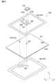
- FIG. 1 is a perspective view of an RFID tag according to a first embodiment of the present disclosure
- 1 is a top view of an RFID tag according to a first embodiment
- FIG. 1 is an exploded perspective view of an RFID tag according to a first embodiment
- Schematic diagram of an RFID tag according to Comparative Example 1 Schematic diagram of an RFID tag according to a first embodiment
- FIG. 13 is an exploded perspective view of an RFID tag according to Comparative Example 2.
- 1 is a top view of an RFID tag according to a second embodiment of the present invention
- FIG. 13 is an exploded perspective view of an RFID tag according to a second embodiment of the present invention
- FIG. 13 is a perspective view of an RFID tag according to a second embodiment of the present disclosure.
- FIG. 13 is an exploded perspective view of an RFID tag according to a second embodiment.
- FIG. 13 is a perspective view of an RFID tag according to a third embodiment of the present disclosure.
- 13 is a top view of an RFID tag according to the third embodiment.
- FIG. 13 is an exploded perspective view of an RFID tag according to a third embodiment.
- Fig. 1 is a perspective view of an RFID tag according to a first embodiment of the present disclosure.
- Fig. 2 is a top view of the RFID tag according to the first embodiment.
- Fig. 3 is an exploded perspective view of the RFID tag according to the first embodiment.
- the X-axis direction indicates the width direction of the RFID tag
- the Y-axis direction indicates the depth direction
- the Z-axis direction indicates the thickness direction.
- the RFID (Radio Frequency IDentification) tag 10 has a substrate 12, an RFIC (Radio Frequency integrated circuit) chip 14 provided on the substrate 12, and a coil conductor 16 electrically connected to the RFIC chip 14.
- RFIC Radio Frequency integrated circuit
- the RFIC chip 14 is configured to perform wireless communication with an external device using the coil conductor 16.
- the RFIC chip 14 has first and second terminals 14a, 14b that are electrically connected to the coil conductor 16.
- the RFIC chip 14 is provided on the first surface 12a of the substrate 12. Specifically, first, a first land conductor 18 electrically connected to one end of the coil conductor 16, and a second land conductor 20 electrically connected to the other end of the coil conductor 16 are provided on the first surface 12a of the substrate 12. These first and second land conductors 18, 20 are, for example, conductor patterns.
- the first terminal 14a of the RFIC chip 14 faces the first land conductor 18 and is fixed while being electrically connected to the first land conductor 18, for example, via a solder material.
- the second terminal 14b of the RFIC chip 14 faces the second land conductor 20 and is fixed while being electrically connected to the second land conductor 20, for example, via a solder material.
- the coil conductor 16 functions as an antenna when the RFIC chip 14 communicates wirelessly with an external device.
- the coil conductor 16 includes a first spiral conductor 22 provided on the first surface 12a of the substrate 12, and a second spiral conductor 24 provided on the second surface 12b of the substrate 12.
- first spiral conductor 22 and the second spiral conductor 24 partially overlap each other.
- These first and second spiral conductors 22, 24 are, for example, conductor patterns.
- the coil conductor 16 includes an interlayer connection conductor portion 26, such as a through-hole conductor, that penetrates the substrate 12 in the thickness direction (Z-axis direction) and electrically connects one end 22a of the first spiral conductor 22 and one end 24a of the second spiral conductor 24.
- an interlayer connection conductor portion 26 such as a through-hole conductor, that penetrates the substrate 12 in the thickness direction (Z-axis direction) and electrically connects one end 22a of the first spiral conductor 22 and one end 24a of the second spiral conductor 24.
- the RFIC chip 14 As shown in FIG. 2, in a plan view of the substrate 12 (viewed in the Z-axis direction), the RFIC chip 14, the first land conductor 18, and the second land conductor 20 are arranged within the opening 16a of the coil conductor 16. In particular, the RFIC chip 14 is arranged in the center of the opening 16a.
- a first connecting conductor 28 is provided on the first surface 12a of the substrate 12 to electrically connect the other end 22b of the first spiral conductor 22 in the coil conductor 16 to the first land conductor 18.
- the first connecting conductor 28 is, for example, a conductor pattern.
- a second connecting conductor 30 is provided on the second surface 12b of the substrate 12 to electrically connect the other end 24b of the second spiral conductor 24 in the coil conductor 16 to the second land conductor 20.
- the second connecting conductor 30 is, for example, a conductor pattern.
- the RFIC chip 14 and the coil conductor 16 are electrically connected by such first and second connecting conductors 28, 30.
- the first connecting conductor 28 and the second connecting conductor 30 are provided on the first and second surfaces 12a, 12b, respectively, of the substrate 12 so as to at least partially overlap when viewed in a plan view of the substrate 12 (viewed in the Z-axis direction). More preferably, the first and second connecting conductors 28, 30 are provided on the substrate 12 so as to overlap as much as possible. In the case of the first embodiment, the overlapping portions 28a, 30a of the first connecting conductor 28 and the second connecting conductor 30 extend linearly in the same direction. The reason why the first connecting conductor 28 and the second connecting conductor 30 partially overlap each other will be described later.
- a land support conductor 34 that supports the first land conductor 18 and the second land conductor 20 is provided on the second surface 12b of the substrate 12.
- the land support conductor 34 is a part of the second connection conductor 30.
- the land support conductor 34 overlaps both the first land conductor 18 and the second land conductor 20 in a planar view of the substrate 12 (in the Z-axis direction). In other words, in a planar view of the substrate 12, the first land conductor 18 and the second land conductor 20 are located within the contour of the land support conductor 34.
- Such a land support conductor 34 prevents the electrical connection between the first and second land conductors 18, 20 and the RFIC chip 14 from being cut off. This is because the second spiral conductor 24 is present on the surface 12b side of the substrate 12, and the first and second land conductors 18, 20 are suspended in the air due to the conductor thickness (e.g., 20 ⁇ m thick) of this spiral conductor 24. However, due to the presence of the land support conductor 34, the first and second land conductors 18, 20 are at the same height and do not float in the air. Therefore, in the case of solder connection, the solder is applied without bending the substrate 12 due to the pressure conditions of the solder squeegee, so poor connection does not occur between the RFIC chip 14 and the first and second land conductors 18, 20.
- the RFID tag 10 when the RFID tag 10 is attached to the surface of an object via the second surface 12b of the substrate 12, the presence of the land support conductor 34 makes the distance from the first land conductor 18 to the object the same as the distance from the second land conductor 20 to the object. Therefore, the RFID tag 10 can be attached to the object without the RFIC chip 14 being tilted.
- the land support conductor 34 when the land support conductor 34 is not present, the second spiral conductor 24 is present on the surface 12b side of the substrate 12, but due to the conductor thickness of this spiral conductor 24, the first and second land conductors 18, 20 are connected to the RFIC chip 14 in a floating state in the air. For this reason, the height of the first and second land conductors 18, 20 is unstable, and in the case of solder connection, the solder is applied as the substrate 12 bends depending on the pressure conditions of the solder squeegee, making the amount of solder unstable, which causes poor connection between the RFIC chip 14 and the first and second land conductors 18, 20. This can also occur when connecting ICs while applying a load, such as in ACP connection or ultrasonic welding.
- the RFIC chip 14 will tilt when the RFID tag 10 is attached to the surface of the object. This is because the distance from the first land conductor 18 to the object is smaller than the distance from the second land conductor 20 to the object due to the absence of the land support conductor 34. If the RFIC chip 14 tilts, for example, the electrical connection between the second terminal 14b and the second land conductor 20 may be broken.
- FIG. 4 is a schematic diagram of an RFID tag in Comparative Example 1.
- FIG. 5 is a schematic diagram of an RFID tag in Example 1. The RFID tag shown in FIG. 5 corresponds to a simplified version of the RFID tag 10 according to the first embodiment shown in FIGS. 1 to 3.
- the RFID tag 110 of Comparative Example 1 has a coil conductor 116 and an RFIC chip 114 disposed within an opening 116a of the coil conductor 116.
- the RFID tag 110 also has a first connecting conductor 128 that electrically connects one end of the coil conductor 116 to the RFIC chip 114, and a second connecting conductor 130 that electrically connects the other end of the coil conductor 116 to the RFIC chip 114.
- the first and second connecting conductors 128, 130 extend in opposite directions from the RFIC chip 114 and do not overlap in a planar view.
- magnetic flux f1 is generated by current i1 flowing through the coil conductor 116.
- Magnetic flux f2 is generated by current i2 flowing through the first connecting conductor 128, the RFIC chip 114, and the second connecting conductor 130. Note that current i1 and current i2 are the same current.
- the first connecting conductor 228 and the second connecting conductor 230 extend linearly in the same direction from the RFIC chip 214 and partially overlap each other (note that in FIG. 5, the first connecting conductor 228 and the second connecting conductor 230 are shown in a non-overlapping state because they would be indistinguishable if they overlapped).
- a magnetic flux f1 is generated by a current i1 flowing through the coil conductor 216.
- a magnetic flux is also generated by a current i2 flowing through the first connecting conductor 228, the RFIC chip 214, and the second connecting conductor 230.
- the direction of the current i2 flowing through the first connecting conductor 228 and the direction of the current i2 flowing through the second connecting conductor 230 are opposite to each other, the magnetic flux generated in the first connecting conductor 228 and the magnetic flux generated in the second connecting conductor 230 cancel each other out.
- the magnetic flux f1 passing through the opening 216a of the coil conductor 216 is not substantially canceled out by the magnetic flux generated in the first and second connecting conductors 228 and 230.
- the communication distance of the RFID tag 210 of the first embodiment is longer than that of the RFID tag 110 of the first comparative example.
- the inventors verified this effect through simulations.
- Figure 6 is a top view of the model of the RFID tag of Comparative Example 2 used in the simulation.
- Figure 7 is an exploded perspective view of the model of the RFID tag of Comparative Example 2.
- Figure 8 is a top view of the model of the RFID tag of Example 2 used in the simulation.
- Figure 9 is an exploded perspective view of the model of the RFID tag of Example 2.
- the coil conductor 316 includes a first spiral conductor 322 provided on the first surface 312a of the substrate 312 and a second spiral conductor 324 provided on the second surface 312b.
- the coil conductor 316 also includes an interlayer connection conductor 326 that electrically connects the outer end of the first spiral conductor 322 and the outer end of the second spiral conductor 324.
- the RFIC chip 314 is disposed in the center of the opening 316a of the coil conductor 316 in a plan view (Z-axis direction view) of the substrate 312.
- the first terminal 314a of the RFIC chip 314 is electrically connected to the inner end of the first spiral conductor 322 via a first connection conductor 328.
- the second terminal 314b of the RFIC chip 314 is electrically connected to the inner end of the second spiral conductor 324 via the second connecting conductor 330 and the interlayer connecting conductor 332.
- the first connecting conductor 328 and the second connecting conductor 330 do not overlap when viewed in a plan view (Z-axis direction) of the substrate 312.
- the coil conductor 416 includes a first spiral conductor 422 provided on the first surface 412a of the substrate 412 and a second spiral conductor 424 provided on the second surface 412b.
- the coil conductor 416 also includes an interlayer connection conductor 426 that electrically connects the outer end of the first spiral conductor 422 and the outer end of the second spiral conductor 424.
- the RFIC chip 414 is disposed in the center of the opening 416a of the coil conductor 416 in a plan view (Z-axis direction view) of the substrate 412.
- the first terminal 414a of the RFIC chip 414 is electrically connected to the inner end of the first spiral conductor 422 via a first connection conductor 428.
- the second terminal 414b of the RFIC chip 414 is electrically connected to the inner end of the second spiral conductor 424 via the second connecting conductor 430 and the interlayer connecting conductor 432.
- the first connecting conductor 428 and the second connecting conductor 430 partially overlap each other in a plan view (viewed in the Z-axis direction) of the substrate 412.
- the substrate 312 and RFIC chip 314 in Comparative Example 2 are the same as the substrate 412 and RFIC chip 414 in Example 2.
- the material of the conductors such as the coil conductor 316 in Comparative Example 2 is the same as the material of the conductors such as the coil conductor 416 in Example 2. Under these conditions, the inventors simulated the communication distances of the RFID tag 310 in Comparative Example 2 and the RFID tag 410 in Example 2.
- the communication distance of the RFID tag 310 of Comparative Example 2 was 10.5 mm, and the communication distance of the RFID tag 410 of Example 2 was 12.5 mm.
- This simulation result shows that the communication distance of the RFID tag is improved if the first connecting conductor and the second connecting conductor at least partially overlap when viewed in a planar view of the substrate.
- the coil conductor 16 and the RFIC chip 14 can be electrically connected while suppressing a decrease in communication distance.
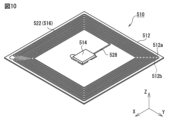
- Fig. 10 is a perspective view of an RFID tag according to a second embodiment of the present disclosure
- Fig. 11 is a top view of the RFID tag according to the second embodiment
- Fig. 12 is an exploded perspective view of the RFID tag according to the second embodiment.
- an RFID tag 510 has a substrate 512, an RFIC chip 514, and a coil conductor 516.
- the coil conductor 516 includes a first spiral conductor 522 provided on a first surface 512a of the substrate 512, a second spiral conductor 524 provided on a second surface 512b of the substrate 512, and an interlayer connection conductor 526 that electrically connects the outer circumferential end of the first spiral conductor 522 and the outer circumferential end of the second spiral conductor 524.
- a first connection conductor 528 is provided on the first surface 512a of the substrate 512, electrically connecting the inner end of the first spiral conductor 522 to the first terminal 514a of the RFIC chip 514.
- the first connection conductor 528 is electrically connected to the first terminal 514a of the RFIC chip 514 via the first land conductor 518.
- a second connection conductor 530 is provided on the second surface 512b of the substrate 512, electrically connecting the inner end of the second spiral conductor 524 to the second terminal 514b of the RFIC chip 514.
- the second connection conductor 530 is electrically connected to the second terminal 514b of the RFIC chip 514 via the interlayer connection conductor 532 and the second land conductor 520.
- the first connecting conductor 528 and the second connecting conductor 530 overlap each other in a plan view (Z-axis direction view) on the substrate 512. In the case of the present embodiment 2, the first connecting conductor 528 and the second connecting conductor 530 overlap each other in many areas.
- the RFID tag 510 of this second embodiment can electrically connect the coil conductor 516 and the RFIC chip 514 while suppressing a decrease in the communication distance.
- the number of turns in the coil conductor 516 of the RFID tag 510 of the present embodiment 2 is greater than the number of turns in the coil conductor 16 of the RFID tag 10 of the above-mentioned embodiment 1. This is because the RFID tag 10 of the above-mentioned embodiment 1 and the RFID tag 510 of the present embodiment 2 differ in communication frequency, and therefore the required inductance of the coil conductor is different. Also, in the case of the present embodiment 2, the first spiral conductor 522 in the coil conductor 516 differs from the second spiral conductor 524 in that the corners are curved convexly toward the center in order to fine-tune the inductance of the coil conductor 516 to an appropriate value.
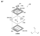
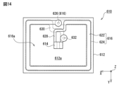
- FIG. 13 is a perspective view of an RFID tag according to a third embodiment of the present disclosure
- Fig. 14 is a top view of the RFID tag according to the third embodiment
- Fig. 15 is an exploded perspective view of the RFID tag according to the third embodiment.
- an RFID tag 610 has a substrate 612, an RFIC chip 614, and a coil conductor 616.
- the coil conductor 616 includes a first spiral conductor 622 provided on a first surface 612a of the substrate 612, a second spiral conductor 624 provided on a second surface 612b of the substrate 612, and an interlayer connection conductor 626 that electrically connects one end of the first spiral conductor 622 and one end of the second spiral conductor 624.
- a first connection conductor 628 is provided on the first surface 612a of the substrate 612, electrically connecting the other end of the first spiral conductor 622 to the first terminal 614a of the RFIC chip 614.
- the first connection conductor 628 is electrically connected to the first terminal 614a of the RFIC chip 614 via the first land conductor 618.
- a second connection conductor 630 is provided on the second surface 612b of the substrate 612, electrically connecting the other end of the second spiral conductor 624 to the second terminal 614b of the RFIC chip 614.
- the second connection conductor 630 is electrically connected to the second terminal 614b of the RFIC chip 614 via the interlayer connection conductor 632 and the second land conductor 620.
- the first connecting conductor 628 and the second connecting conductor 630 overlap each other in a plan view (Z-axis direction view) on the substrate 612. Furthermore, unlike the first connecting conductor 28 and the second connecting conductor 30 of the above-mentioned embodiment 1, the first connecting conductor 628 and the second connecting conductor 630 cross each other. Therefore, a gap is generated between the part of the first connecting conductor 628 and the part of the second connecting conductor 630 that extend between the intersection and the RFIC chip 614. Due to this gap, the magnetic fields generated in the parts of the first connecting conductor 628 and the second connecting conductor 630 cannot cancel each other out. However, since the magnetic fields generated at the intersection can cancel each other out, the communication distance is longer than when the first connecting conductor and the second connecting conductor do not overlap at all (for example, in the above-mentioned comparative examples 1 and 2).
- the RFID tag 610 of this third embodiment can electrically connect the coil conductor 616 and the RFIC chip 614 while suppressing a decrease in the communication distance.
- the coil conductor 16 is composed of a first spiral conductor 22 provided on the first surface 12a of the substrate 12 and a second spiral conductor 24 provided on the second surface 12b of the substrate 12.
- the embodiments of the present disclosure are not limited to this.
- the coil conductor may be composed of a spiral conductor formed on only one of the first and second surfaces of the substrate.
- the first aspect is a substrate having a first surface and a second surface opposite the first surface; a coil conductor including a first spiral conductor provided on the first surface of the substrate, a second spiral conductor provided on the second surface of the substrate, and an interlayer connection conductor penetrating the substrate and electrically connecting one end of the first spiral conductor and one end of the second spiral conductor; an RFIC chip provided on the substrate so as to be positioned within an opening of the coil conductor in a plan view of the substrate, the RFIC chip including first and second terminals; a first connection conductor provided on a first surface of the base material and electrically connecting the other end of the first spiral conductor and the first terminal of the RFIC chip; a second connection conductor provided on a second surface of the base material and electrically connecting the other end of the second spiral conductor and the second terminal of the RFIC chip; In the RFID tag, the first connecting conductor and the second connecting conductor at least partially overlap each other in a plan view of the base material.
- the second aspect is In the RFID tag of the first aspect, in a plan view of the base material, the overlapping portions of the first connecting conductor and the second connecting conductor extend in the same direction.
- the third aspect is In the RFID tag of the first aspect, the first connecting conductor and the second connecting conductor cross each other in a plan view of the base material.
- the fourth aspect is a first land conductor provided on the first surface of the base material, facing and electrically connected to the first terminal of the RFIC chip; a second land conductor provided on the first surface of the base material, facing and electrically connected to the second terminal of the RFIC chip, the first connection conductor is electrically connected to the first land conductor;
- the RFID tag according to any one of the first to third aspects, wherein the second connection conductor is electrically connected to the second land conductor.
- the fifth aspect is A fourth aspect of the RFID tag further includes a land support conductor that is provided on the second surface of the substrate so as to face both the first land conductor and the second land conductor in a planar view of the substrate, and supports the first and second land conductors.
- the sixth aspect is A fifth aspect of the RFID tag, wherein the land support conductor is a part of the second connecting conductor.
- the first connecting conductor and the second connecting conductor are at least partially overlapped with each other in a plan view of the substrate, thereby canceling out the magnetic fields generated by the first connecting conductor and the second connecting conductor.
- the predetermined distance is, for example, a distance smaller than the width of the first and second connecting conductors.
- a capacitance is formed between them. This capacitance can reduce the inductance of the coil conductor, that is, the number of turns of the coil conductor can be reduced, which has the advantage of allowing the RFID tag to be made smaller.
- This disclosure is applicable to an RFID tag having a coil conductor and an RFIC chip disposed within an opening in the coil conductor.
Landscapes
- Engineering & Computer Science (AREA)
- Microelectronics & Electronic Packaging (AREA)
- Computer Hardware Design (AREA)
- Physics & Mathematics (AREA)
- General Physics & Mathematics (AREA)
- Theoretical Computer Science (AREA)
- Computer Networks & Wireless Communication (AREA)
- Coils Or Transformers For Communication (AREA)
Priority Applications (3)
| Application Number | Priority Date | Filing Date | Title |
|---|---|---|---|
| DE212023000396.1U DE212023000396U1 (de) | 2022-12-12 | 2023-12-01 | RFID-Etikett |
| JP2024564286A JP7786616B2 (ja) | 2022-12-12 | 2023-12-01 | Rfidタグ |
| US19/090,933 US20250225362A1 (en) | 2022-12-12 | 2025-03-26 | Rfid tag |
Applications Claiming Priority (2)
| Application Number | Priority Date | Filing Date | Title |
|---|---|---|---|
| JP2022-197889 | 2022-12-12 | ||
| JP2022197889 | 2022-12-12 |
Related Child Applications (1)
| Application Number | Title | Priority Date | Filing Date |
|---|---|---|---|
| US19/090,933 Continuation US20250225362A1 (en) | 2022-12-12 | 2025-03-26 | Rfid tag |
Publications (1)
| Publication Number | Publication Date |
|---|---|
| WO2024128039A1 true WO2024128039A1 (ja) | 2024-06-20 |
Family
ID=91485684
Family Applications (1)
| Application Number | Title | Priority Date | Filing Date |
|---|---|---|---|
| PCT/JP2023/043158 Ceased WO2024128039A1 (ja) | 2022-12-12 | 2023-12-01 | Rfidタグ |
Country Status (4)
| Country | Link |
|---|---|
| US (1) | US20250225362A1 (https=) |
| JP (1) | JP7786616B2 (https=) |
| DE (1) | DE212023000396U1 (https=) |
| WO (1) | WO2024128039A1 (https=) |
Citations (2)
| Publication number | Priority date | Publication date | Assignee | Title |
|---|---|---|---|---|
| US20160241306A1 (en) * | 2015-02-17 | 2016-08-18 | Byeong-Taek MOON | Portable device and near field communication chip |
| WO2021085269A1 (ja) * | 2019-10-28 | 2021-05-06 | 京セラ株式会社 | Rfidタグ用基板およびrfidタグならびにrfidシステム |
-
2023
- 2023-12-01 DE DE212023000396.1U patent/DE212023000396U1/de active Active
- 2023-12-01 JP JP2024564286A patent/JP7786616B2/ja active Active
- 2023-12-01 WO PCT/JP2023/043158 patent/WO2024128039A1/ja not_active Ceased
-
2025
- 2025-03-26 US US19/090,933 patent/US20250225362A1/en active Pending
Patent Citations (2)
| Publication number | Priority date | Publication date | Assignee | Title |
|---|---|---|---|---|
| US20160241306A1 (en) * | 2015-02-17 | 2016-08-18 | Byeong-Taek MOON | Portable device and near field communication chip |
| WO2021085269A1 (ja) * | 2019-10-28 | 2021-05-06 | 京セラ株式会社 | Rfidタグ用基板およびrfidタグならびにrfidシステム |
Also Published As
| Publication number | Publication date |
|---|---|
| JPWO2024128039A1 (https=) | 2024-06-20 |
| JP7786616B2 (ja) | 2025-12-16 |
| DE212023000396U1 (de) | 2025-08-25 |
| US20250225362A1 (en) | 2025-07-10 |
Similar Documents
| Publication | Publication Date | Title |
|---|---|---|
| JP3957000B1 (ja) | 基板実装用アンテナコイル及びアンテナ装置 | |
| JP4978756B2 (ja) | 通信端末 | |
| CN101859923B (zh) | 天线 | |
| US8698685B2 (en) | Antenna device | |
| CN205429169U (zh) | 天线装置及电子设备 | |
| JP2008245132A (ja) | 無線装置 | |
| CN205039241U (zh) | 无线通信装置 | |
| JP2017038350A (ja) | アンテナ装置、電子機器およびアンテナ装置の実装方法 | |
| US11269024B2 (en) | Magnetic sensor | |
| JP6589815B2 (ja) | アンテナ装置 | |
| JP2016178449A (ja) | アンテナ装置 | |
| US12131859B2 (en) | Coil structure | |
| JP6115285B2 (ja) | コイル部品 | |
| JP7786616B2 (ja) | Rfidタグ | |
| TW202123529A (zh) | 天線 | |
| JP6627252B2 (ja) | アンテナ装置 | |
| US11461612B2 (en) | RFID tag and RFID tag-equipped article | |
| WO2022038995A1 (ja) | アンテナ装置 | |
| JP6809133B2 (ja) | アンテナ装置 | |
| CN114784491A (zh) | 线圈部件和具备其的无线电力传输设备 | |
| WO2012144077A1 (ja) | アンテナ装置、通信モジュール、携帯電子機器及びそれを利用した通信方法 | |
| US20240128006A1 (en) | Laminated coil component | |
| JP2018200926A (ja) | 電子機器 | |
| KR20250111057A (ko) | 전자 부품 | |
| JP2008125036A (ja) | アンテナ装置及びそれを用いたアンテナ実装基板 |
Legal Events
| Date | Code | Title | Description |
|---|---|---|---|
| 121 | Ep: the epo has been informed by wipo that ep was designated in this application |
Ref document number: 23903328 Country of ref document: EP Kind code of ref document: A1 |
|
| WWE | Wipo information: entry into national phase |
Ref document number: 2024564286 Country of ref document: JP |
|
| WWE | Wipo information: entry into national phase |
Ref document number: 212023000396 Country of ref document: DE |
|
| WWG | Wipo information: grant in national office |
Ref document number: 212023000396 Country of ref document: DE |
|
| 122 | Ep: pct application non-entry in european phase |
Ref document number: 23903328 Country of ref document: EP Kind code of ref document: A1 |