WO2024128011A1 - 半導体装置 - Google Patents
半導体装置 Download PDFInfo
- Publication number
- WO2024128011A1 WO2024128011A1 PCT/JP2023/042902 JP2023042902W WO2024128011A1 WO 2024128011 A1 WO2024128011 A1 WO 2024128011A1 JP 2023042902 W JP2023042902 W JP 2023042902W WO 2024128011 A1 WO2024128011 A1 WO 2024128011A1
- Authority
- WO
- WIPO (PCT)
- Prior art keywords
- lead
- back surface
- sealing resin
- leads
- semiconductor element
- Prior art date
- Legal status (The legal status is an assumption and is not a legal conclusion. Google has not performed a legal analysis and makes no representation as to the accuracy of the status listed.)
- Ceased
Links
Images










Classifications
-
- H—ELECTRICITY
- H10—SEMICONDUCTOR DEVICES; ELECTRIC SOLID-STATE DEVICES NOT OTHERWISE PROVIDED FOR
- H10W—GENERIC PACKAGES, INTERCONNECTIONS, CONNECTORS OR OTHER CONSTRUCTIONAL DETAILS OF DEVICES COVERED BY CLASS H10
- H10W70/00—Package substrates; Interposers; Redistribution layers [RDL]
- H10W70/40—Leadframes
- H10W70/421—Shapes or dispositions
-
- H—ELECTRICITY
- H10—SEMICONDUCTOR DEVICES; ELECTRIC SOLID-STATE DEVICES NOT OTHERWISE PROVIDED FOR
- H10W—GENERIC PACKAGES, INTERCONNECTIONS, CONNECTORS OR OTHER CONSTRUCTIONAL DETAILS OF DEVICES COVERED BY CLASS H10
- H10W70/00—Package substrates; Interposers; Redistribution layers [RDL]
- H10W70/40—Leadframes
- H10W70/421—Shapes or dispositions
- H10W70/424—Cross-sectional shapes
-
- H—ELECTRICITY
- H10—SEMICONDUCTOR DEVICES; ELECTRIC SOLID-STATE DEVICES NOT OTHERWISE PROVIDED FOR
- H10W—GENERIC PACKAGES, INTERCONNECTIONS, CONNECTORS OR OTHER CONSTRUCTIONAL DETAILS OF DEVICES COVERED BY CLASS H10
- H10W72/00—Interconnections or connectors in packages
-
- H—ELECTRICITY
- H10—SEMICONDUCTOR DEVICES; ELECTRIC SOLID-STATE DEVICES NOT OTHERWISE PROVIDED FOR
- H10W—GENERIC PACKAGES, INTERCONNECTIONS, CONNECTORS OR OTHER CONSTRUCTIONAL DETAILS OF DEVICES COVERED BY CLASS H10
- H10W74/00—Encapsulations, e.g. protective coatings
-
- H—ELECTRICITY
- H10—SEMICONDUCTOR DEVICES; ELECTRIC SOLID-STATE DEVICES NOT OTHERWISE PROVIDED FOR
- H10W—GENERIC PACKAGES, INTERCONNECTIONS, CONNECTORS OR OTHER CONSTRUCTIONAL DETAILS OF DEVICES COVERED BY CLASS H10
- H10W74/00—Encapsulations, e.g. protective coatings
- H10W74/10—Encapsulations, e.g. protective coatings characterised by their shape or disposition
- H10W74/111—Encapsulations, e.g. protective coatings characterised by their shape or disposition the semiconductor body being completely enclosed
Definitions
- This disclosure relates to a semiconductor device.
- QFN Quadrature For Non-Lead Package
- Patent Document 1 discloses an example of a QFN semiconductor device.
- the semiconductor device disclosed in this document comprises multiple leads, a semiconductor element, and sealing resin.
- the semiconductor element is supported by the multiple leads.
- the sealing resin covers a portion of each lead and the semiconductor element.
- the sealing resin and the semiconductor element are rectangular in plan view.
- this semiconductor device the end faces of the multiple leads are exposed so as to be flush with the side surface of the sealing resin (packaging material in Patent Document 1). In addition, the back surfaces of the multiple leads are exposed so as to be flush with the bottom surface of the sealing resin. Therefore, compared to a QFP (Quad Flat Package) in which the leads protrude from the side surface of the sealing resin, this semiconductor device has the advantage that it is possible to miniaturize the semiconductor device and reduce the mounting area on the wiring board.
- QFP Quad Flat Package
- the center of the semiconductor element in a planar view may be positioned offset from the center of the encapsulating resin in a planar view. If the center of the semiconductor element is offset from the center of the encapsulating resin, this offset may cause a bias in the stress that occurs in the solder joined to the back surface of the lead when the semiconductor device is mounted on the wiring board. In areas where the solder stress is concentrated when the semiconductor device is mounted, there is a concern that cracks may occur in the solder or the solder may peel off.
- An object of the present disclosure is to provide a semiconductor device that is an improvement over conventional semiconductor devices.
- an object of the present disclosure is to provide a semiconductor device that is suitable for suppressing stress concentration during mounting on a wiring board and improving mounting reliability in a configuration in which the center of the semiconductor element is offset from the center of the semiconductor element.
- the semiconductor device provided by the first aspect of the present disclosure includes a plurality of leads, each of which has a main surface facing one side in a thickness direction, a back surface facing the other side in the thickness direction, and an end surface connected to the back surface and facing a direction perpendicular to the thickness direction, a semiconductor element supported by the main surfaces of the plurality of leads and conductive to at least one of the plurality of leads, and a sealing resin covering a portion of each of the plurality of leads and at least a portion of the semiconductor element.
- the sealing resin is rectangular when viewed in the thickness direction, and has a first corner portion located on one side of a first direction perpendicular to the thickness direction, a second corner portion located on the other side of the first direction, a bottom surface facing the other side in the thickness direction, and a first side surface each connected to the bottom surface and facing one side of the first direction, a second side surface facing the other side of the first direction, a third side surface facing one side of a second direction perpendicular to the thickness direction and the first direction, and a fourth side surface facing the other side of the second direction.
- the main surface is covered with the sealing resin, and the back surface is exposed from the bottom surface.
- the multiple leads include a first lead located closest to the first corner and conducting to the semiconductor element.
- the end face of the first lead is exposed from at least one of the first side surface, the third side surface, and the fourth side surface.
- the area of the back surface of the first lead is larger than the area of the back surface of the lead located next to the first lead and conducting to the semiconductor element, or the area of the back surface of the lead located closest to the second corner and conducting to the semiconductor element.
- the semiconductor device provided by the second aspect of the present disclosure includes a plurality of leads, each of which has a main surface facing one side in a thickness direction, a back surface facing the other side in the thickness direction, and an end surface connected to the back surface and facing a direction perpendicular to the thickness direction, a semiconductor element supported by the main surfaces of the leads and conductive to at least one of the leads, and a sealing resin covering a portion of each of the leads and at least a portion of the semiconductor element.
- the sealing resin is rectangular when viewed in the thickness direction, and has a first corner portion located on one side of a first direction perpendicular to the thickness direction, a second corner portion located on the other side of the first direction, a bottom surface facing the other side in the thickness direction, and a first side surface each connected to the bottom surface and facing one side of the first direction, a second side surface facing the other side of the first direction, a third side surface facing one side of a second direction perpendicular to the thickness direction and the first direction, and a fourth side surface facing the other side of the second direction.
- the main surface is covered with the sealing resin, and the back surface is exposed from the bottom surface.
- the multiple leads include a first lead located closest to the first corner.
- the end face of the first lead is exposed from at least one of the first side surface, the third side surface, and the fourth side surface.
- the area of the back surface of the first lead is larger than the area of the back surface of the lead located next to the first lead, or the area of the back surface of the lead located closest to the second corner.
- the semiconductor device disclosed herein can suppress stress concentration during mounting on a wiring board, improving mounting reliability.
- FIG. 1 is a perspective view showing a semiconductor device according to a first embodiment of the present disclosure.
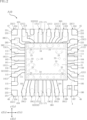
- FIG. 2 is a plan view (through a sealing resin) showing the semiconductor device according to the first embodiment of the present disclosure.
- FIG. 3 is a plan view (with a semiconductor element and a sealing resin transparent) showing the semiconductor device according to the first embodiment of the present disclosure.
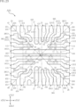
- FIG. 4 is a bottom view showing the semiconductor device according to the first embodiment of the present disclosure.
- FIG. 5 is a front view showing the semiconductor device according to the first embodiment of the present disclosure.
- FIG. 6 is a rear view showing the semiconductor device according to the first embodiment of the present disclosure.
- FIG. 7 is a right side view showing the semiconductor device according to the first embodiment of the present disclosure.
- FIG. 1 is a perspective view showing a semiconductor device according to a first embodiment of the present disclosure.
- FIG. 2 is a plan view (through a sealing resin) showing the semiconductor device according to the first embodiment of the present disclosure.
- FIG. 3 is a
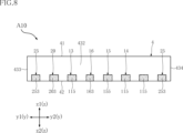
- FIG. 8 is a left side view showing the semiconductor device according to the first embodiment of the present disclosure.
- FIG. 9 is a partially enlarged view of FIG.
- FIG. 10 is a partially enlarged view of FIG.
- FIG. 11 is a cross-sectional view taken along line XI-XI in FIG.
- FIG. 12 is a cross-sectional view taken along line XII-XII in FIG.
- FIG. 13 is a cross-sectional view taken along line XIII-XIII in FIG.
- FIG. 14 is a cross-sectional view taken along line XIV-XIV in FIG.
- FIG. 15 is a cross-sectional view taken along line XV-XV in FIG.
- FIG. 10 is a partially enlarged view of FIG.
- FIG. 11 is a cross-sectional view taken along line XI-XI in FIG.
- FIG. 12 is a cross-sectional view taken along line XII-XII in FIG.
- FIG. 13 is
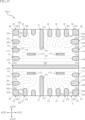
- FIG. 16 is a plan view (with a semiconductor element and a sealing resin transparent) showing a semiconductor device according to a first modification of the first embodiment.
- FIG. 17 is a bottom view showing a semiconductor device according to a first modification of the first embodiment.
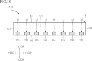
- FIG. 18 is a right side view showing a semiconductor device according to a first modification of the first embodiment.
- FIG. 19 is a plan view (with a semiconductor element and a sealing resin transparent) showing a semiconductor device according to a second embodiment of the present disclosure.
- FIG. 20 is a bottom view showing the semiconductor device according to the second embodiment of the present disclosure.
- FIG. 21 is a rear view showing the semiconductor device according to the second embodiment of the present disclosure.
- FIG. 22 is a right side view showing the semiconductor device according to the second embodiment of the present disclosure.
- FIG. 23 is a plan view (with a semiconductor element and a sealing resin transparent) showing a semiconductor device according to a first modification of the second embodiment.
- FIG. 24 is a bottom view showing a semiconductor device according to a first modification of the second embodiment.
- FIG. 25 is a front view showing a semiconductor device according to a first modification of the second embodiment.
- FIG. 26 is a rear view showing the semiconductor device according to the first modification of the second embodiment.
- FIG. 27 is a right side view showing a semiconductor device according to a first modification of the second embodiment.
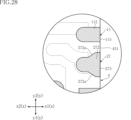
- FIG. 28 is a partially enlarged bottom view showing another example of the configuration of the first lead.
- FIG. 29 is a partially enlarged bottom view showing another example of the configuration of the first lead.
- an object A is formed on an object B" and “an object A is formed on an object B” include “an object A is formed directly on an object B” and “an object A is formed on an object B with another object interposed between the object A and the object B” unless otherwise specified.
- an object A is disposed on an object B” and “an object A is disposed on an object B” include “an object A is disposed directly on an object B” and “an object A is disposed on an object B with another object interposed between the object A and the object B" unless otherwise specified.
- an object A is located on an object B includes “an object A is located on an object B in contact with an object B” and “an object A is located on an object B with another object interposed between the object A and the object B” unless otherwise specified.
- an object A overlaps an object B when viewed in a certain direction includes “an object A overlaps the entire object B” and “an object A overlaps a part of an object B.”
- a surface A faces (one side or the other side of) direction B” is not limited to the case where the angle of surface A with respect to direction B is 90 degrees, but also includes the case where surface A is tilted with respect to direction B.
- the semiconductor device A10 includes a plurality of leads 1, a semiconductor element 3, and a sealing resin 4.
- the package format of the semiconductor device A10 is a QFN (Quad For Non-Lead Package).
- the specific configuration of the semiconductor element 3 is not particularly limited, and in the present embodiment, the semiconductor element 3 is, for example, a flip-chip type LSI (Large Scale Integration) having a switching circuit 321 and a control circuit 322 (each of which will be described in detail later) configured therein.
- LSI Large Scale Integration
- the semiconductor device A10 DC power (voltage) is converted into AC power (voltage) by the switching circuit 321.
- the semiconductor device A10 is used, for example, as one element constituting a circuit of a DC/DC converter.
- FIG. 1 is a perspective view showing the semiconductor device A10.
- FIG. 2 is a plan view showing the semiconductor device A10.
- FIG. 3 is a plan view showing the semiconductor device A10.
- FIG. 4 is a bottom view showing the semiconductor device A10.
- FIG. 5 is a front view showing the semiconductor device A10.
- FIG. 6 is a rear view showing the semiconductor device A10.
- FIG. 7 is a right side view showing the semiconductor device A10.
- FIG. 8 is a left side view showing the semiconductor device A10.
- FIG. 9 and FIG. 10 are partial enlarged views of FIG. 4.
- FIG. 11 is a cross-sectional view taken along line XI-XI in FIG. 3.
- FIG. 10 is a cross-sectional view taken along line X-X in FIG. 3.
- FIG. 11 is a cross-sectional view taken along line XI-XI in FIG. 3.
- FIG. 10 is a cross-sectional view taken along line X-X in FIG. 3.
- FIG. 11 is a
- FIG. 11 is a cross-sectional view taken along line XI-XI in FIG. 3.
- FIG. 12 is a cross-sectional view taken along line XII-XII in FIG. 3.
- FIG. 13 is a cross-sectional view taken along line XIII-XIII in FIG. 3.
- FIG. 14 is a cross-sectional view taken along line XIV-XIV in FIG. 3.
- FIG. 15 is a cross-sectional view taken along line XV-XV in FIG. 3.
- FIG. 2 shows the sealing resin 4 in a see-through manner.
- FIG. 3 shows the semiconductor element 3 and sealing resin 4 in a see-through manner. In these figures, the semiconductor element 3 and sealing resin 4 are shown by imaginary lines (double-dashed lines).
- the thickness direction (direction when viewed from above) of the multiple leads 1 is an example of the "thickness direction" of the present disclosure, and is referred to as the "thickness direction z".
- the direction perpendicular to the thickness direction z (left-right direction in FIG. 2) is referred to as the "first direction x”.
- the direction perpendicular to the thickness direction z and the first direction x (up-down direction in FIG. 2) is referred to as the "second direction y”.
- the semiconductor device A10 is rectangular when viewed in the thickness direction z. As shown in FIGS. 1 to 3, in the illustrated example, the semiconductor device A10 is square when viewed in the thickness direction z.
- the right side in FIG. 2 is an example of the "one side of the first direction" of the present disclosure, and is referred to as the "x1 side of the first direction x”
- the left side in the figure is an example of the "other side of the first direction” of the present disclosure, and is referred to as the "x2 side of the first direction x”
- the upper side in the figure is an example of “one side in the second direction” in this disclosure and is called the “y1 side of the second direction y”
- the lower side in the figure is an example of "the other side in the second direction” in this disclosure and is called the "y2 side of the second direction y.”
- the upper side in the figure is an example of “one side in the thickness direction” in this disclosure and is called the “z1 side of the thickness direction z”
- the lower side in the figure is an example of "the other side in the thickness direction” in this disclosure and is called the “z2 side of the thickness direction z.”
- the multiple leads 1 include multiple leads 11, 12, 13, 14, lead 15, lead 16, a pair of leads 17, lead 18, multiple leads 19, lead 20, multiple leads 21, lead 22, lead 23, and multiple leads 25.
- the multiple leads 1 (multiple leads 11 to 14, lead 15, lead 16, a pair of leads 17, lead 18, multiple leads 19, lead 20, multiple leads 21, lead 22, and lead 23) support the semiconductor element 3 and form terminals for mounting the semiconductor device A10 on a wiring board.
- each of the multiple leads 11 to 14, lead 15, lead 16, a pair of leads 17, lead 18, multiple leads 19, lead 20, multiple leads 21, lead 22, lead 23, and multiple leads 25 is partially covered with the sealing resin 4.
- the multiple leads 11 to 14, lead 15, lead 16, pair of leads 17, lead 18, multiple leads 19, lead 20, multiple leads 21, lead 22, lead 23, and multiple leads 25 are all made of the same lead frame.
- the constituent material of the lead frame is, for example, copper or a copper alloy.
- the multiple leads 11, 12, 13, and 14 are arranged on the x1 side and the x2 side of the first direction x in the semiconductor device A10.
- two (a pair) of leads 11, 12 are arranged on the x1 side of the first direction x
- the other two (a pair) of leads 13, 14 are arranged on the x2 side of the first direction x.
- the multiple leads 11 to 14 each extend approximately in the first direction x.
- the pair of leads 11, 12 located on the x1 side of the first direction x are arranged at an interval in the second direction y.
- the pair of leads 13, 14 located on the x2 side of the first direction x are arranged at an interval in the second direction y.
- Each of the multiple leads 11 to 14 outputs AC power (voltage) converted by the switching circuit 321 configured in the semiconductor element 3.
- each of the multiple leads 11, 12, 13, 14 has a main surface 111, a back surface 112, a back surface 113, a concave surface 114 and an end surface 115.
- the main surface 111 faces the z1 side in the thickness direction z and faces the semiconductor element 3.
- the main surface 111 is covered with the sealing resin 4.
- the semiconductor element 3 is supported by the main surface 111.
- the back surface 112, the back surface 113, and the concave surface 114 face the opposite side to the main surface 111 (the z2 side in the thickness direction z).
- the back surface 112 and the back surface 113 are located apart in the first direction x with the concave surface 114 in between, and are exposed from the sealing resin 4.
- the concave surface 114 is located closer to the z1 side in the thickness direction z than the back surface 112 and the back surface 113, and is closer to the main surface 111 than the back surface 112 and the back surface 113.
- the concave surface 114 is covered with the sealing resin 4.
- the end surface 115 is connected to both the main surface 111 and the back surface 112, and faces the x1 side in the first direction x or the x2 side in the first direction x.
- the end surface 115 is exposed from the sealing resin 4.
- the lead 14 has two back surfaces 112 and two end surfaces 115.
- the back surface 112 and end surface 115 on one side are spaced apart from the back surface 112 and end surface 115 on the other side in the second direction y.
- the main surface 111 on which the semiconductor element 3 is supported may be plated with silver, for example.
- the back surface 112, back surface 113, and end surface 115 exposed from the sealing resin 4 may be plated with tin, for example.
- tin plating multiple metal platings may be used, for example, layered in the order nickel, palladium, and gold.
- lead 15 extends in the first direction x.
- lead 15 is located at the middle of semiconductor device A10 in the second direction y.
- Lead 15 is an input terminal to which DC power (voltage) to be converted in semiconductor device A10 is input.
- Lead 15 is the positive electrode (P terminal).
- the lead 15 has a main surface 151, a back surface 152, a back surface 153, a concave surface 154, an end surface 155, and an end surface 156.
- the main surface 151 faces the same side as the main surfaces 111 of the leads 11 to 14 in the thickness direction z, and faces the semiconductor element 3.
- the main surface 151 is covered with the sealing resin 4.
- the semiconductor element 3 is supported by the main surface 151.
- the back surface 152, the back surface 153, and the concave surface 154 face the opposite side to the main surface 151 (the z2 side in the thickness direction z).
- the back surface 152 and the back surface 153 are located apart in the first direction x with the concave surface 154 in between, and are exposed from the sealing resin 4.
- the back surface 152 is located on the x2 side in the first direction x
- the back surface 153 is located on the x1 side in the first direction x.
- the concave surface 154 is located closer to the z1 side in the thickness direction z than the back surfaces 152 and 153, and is closer to the main surface 151 than the back surfaces 152 and 153.
- the concave surface 154 is covered with the sealing resin 4.
- the end surface 155 is connected to both the main surface 151 and the back surface 152, and faces the x2 side in the first direction x.
- the end surface 156 is connected to both the main surface 151 and the back surface 153, and faces the x1 side in the first direction x. End surface 155 and end surface 156 are exposed from sealing resin 4.
- the main surface 151 on which the semiconductor element 3 is supported may be plated with silver, for example.
- the back surface 152, back surface 153, end surface 155, and end surface 156 exposed from the sealing resin 4 may be plated with tin, for example.
- tin plating multiple metal platings may be used, for example, layered in the order nickel, palladium, and gold.
- the lead 16 extends in the first direction x.
- the lead 16 is located at the middle of the semiconductor device A10 in the second direction y.
- the lead 16 is an input terminal to which the DC power (voltage) to be converted in the semiconductor device A10 is input.
- the lead 16 is the negative electrode (N terminal).
- the lead 16 has a main surface 161, a back surface 162, an end surface 163, and an end surface 164.
- the main surface 161 faces the same side as the main surfaces 111 of the leads 11 to 14 in the thickness direction z, and faces the semiconductor element 3.
- the main surface 161 is covered with the sealing resin 4.
- the semiconductor element 3 is supported by the main surface 161.
- the back surface 162 faces the opposite side to the main surface 161 (the z2 side in the thickness direction z).
- the back surface 162 is exposed from the sealing resin 4.
- the main surface 161 and the back surface 162 are arranged over the entire length of the semiconductor device A10 in the first direction x.
- the end surface 163 is connected to both the main surface 161 and the back surface 162, and faces the x2 side in the first direction x.
- the end surface 164 is connected to both the main surface 161 and the back surface 162, and faces the x1 side in the first direction x.
- the end surface 163 and the end surface 164 are exposed from the sealing resin 4.
- the main surface 161 of the lead 16 on which the semiconductor element 3 is supported may be plated with silver, for example.
- the back surface 162, end surface 163, and end surface 164 exposed from the sealing resin 4 may be plated with tin, for example.
- tin plating multiple metal platings may be used, for example, layered in the order nickel, palladium, and gold.
- the pair of leads 17 are disposed in the middle of the semiconductor device A10 in the first direction x.
- Each of the pair of leads 17 extends in the second direction y.
- One lead 17 is located on the y1 side of the second direction y, and the other lead 17 is located on the y2 side of the second direction y.
- Each of the pair of leads 17 receives, for example, power (voltage) for driving the control circuit 322, or an electrical signal for transmission to the control circuit 322.
- each of the pair of leads 17 has a main surface 171, a back surface 172, and an end surface 173.
- the main surface 171 faces the same side as the main surfaces 111 of the leads 11 to 14 in the thickness direction z, and faces the semiconductor element 3.
- the main surface 171 is covered with the sealing resin 4.
- the semiconductor element 3 is supported by the main surface 171.
- the back surface 172 faces the opposite side to the main surface 171 (the z2 side in the thickness direction z).
- the back surface 172 is exposed from the sealing resin 4.
- the end surface 173 is connected to both the main surface 171 and the back surface 172, and faces in the second direction y. More specifically, the end surface 173 of one lead 17 faces the y1 side in the second direction y, and the end surface 173 of the other lead 17 faces the y2 side in the second direction y.
- the end surface 173 is exposed from the sealing resin 4.
- the main surface 171 on which the semiconductor element 3 is supported may be plated with silver, for example.
- the back surface 172 and end surface 173 exposed from the sealing resin 4 may be plated with tin, for example.
- tin plating multiple metal platings may be used, for example, layered in the order nickel, palladium, and gold.
- the lead 18 is disposed near a corner of the semiconductor device A10 on the x1 side in the first direction x and the y2 side in the second direction y.
- An electrical signal is input to the lead 18 for transmission to the control circuit 322, for example.
- the lead 18 has a main surface 181, back surfaces 182, 183, 184, and end surfaces 185, 186, 187, 188.
- the main surface 181 faces the same side as the main surfaces 111 of the leads 11 to 14 in the thickness direction z, and faces the semiconductor element 3.
- the main surface 181 is covered with the sealing resin 4.
- the semiconductor element 3 is supported by the main surface 181.
- the back surfaces 182, 183, 184 face the opposite side to the main surface 181 (the z2 side in the thickness direction z). Each of the back surfaces 182 to 184 is exposed from the sealing resin 4.
- the back surface 183 is disposed at a corner of the semiconductor device A10 on the x1 side in the first direction x and on the y2 side in the second direction y.
- the back surface 182 is disposed adjacent to the back surface 183 on the y1 side in the second direction y.
- the back surface 184 is disposed adjacent to the back surface 183 on the x2 side in the first direction x.
- the end surface 185 is connected to both the main surface 181 and the back surface 182, and faces the x1 side in the first direction x.
- the end surface 186 is connected to both the main surface 181 and the back surface 183, and faces the x1 side in the first direction x.
- the end surface 187 is connected to both the main surface 181 and the back surface 183, and faces the y2 side in the second direction y.
- the end surface 188 is connected to both the main surface 181 and the back surface 184, and faces the y2 side in the second direction y.
- the end surfaces 185 to 188 are exposed from the sealing resin 4.
- the main surface 181 of the lead 18 on which the semiconductor element 3 is supported may be plated with silver, for example.
- the back surfaces 182-184 and end surfaces 185-188 exposed from the sealing resin 4 may be plated with tin, for example.
- tin plating multiple metal platings may be used, for example nickel, palladium, and gold layered in this order.
- each of the multiple leads 19 has a main surface 191, a back surface 192 and an end surface 193.
- the main surface 191 faces the same side as the main surfaces 111 of the leads 11 to 14 in the thickness direction z, and faces the semiconductor element 3.
- the main surface 191 is covered with the sealing resin 4.
- the semiconductor element 3 is supported by the main surface 191.
- the back surface 192 faces the opposite side to the main surface 191 (the z2 side in the thickness direction z).
- the back surface 192 is exposed from the sealing resin 4.
- the end surface 193 is connected to both the main surface 191 and the back surface 192, and faces the y2 side in the second direction y.
- the end surface 193 is exposed from the sealing resin 4.
- the main surface 191 on which the semiconductor element 3 is supported may be plated with silver, for example.
- the back surface 192 and end surface 193 exposed from the sealing resin 4 may be plated with tin, for example.
- tin plating multiple metal platings may be used, for example, in which nickel, palladium, and gold are layered in this order.
- the lead 20 is arranged on the x2 side of the first direction x in the semiconductor device A10.
- the lead 20 is also arranged in the second direction y, closer to the y1 side of the second direction y.
- An electrical signal is input to the lead 20 to be transmitted to the control circuit 322, for example.
- the lead 20 has a main surface 201, a back surface 202, and an end surface 203.
- the main surface 201 faces the same side as the main surfaces 111 of the leads 11 to 14 in the thickness direction z, and faces the semiconductor element 3.
- the main surface 201 is covered with the sealing resin 4.
- the semiconductor element 3 is supported by the main surface 201.
- the back surface 202 faces the opposite side to the main surface 201 (the z2 side of the thickness direction z).
- the back surface 202 is exposed from the sealing resin 4.
- the end surface 203 is connected to both the main surface 201 and the back surface 202, and faces the x2 side of the first direction x.
- the main surface 201 of the lead 20 on which the semiconductor element 3 is supported may be plated with silver, for example.
- the back surface 202 and end surface 203 exposed from the sealing resin 4 may be plated with tin, for example. Note that instead of tin plating, multiple metal platings may be used, for example nickel, palladium, and gold layered in this order.
- each of the multiple leads 21 has a main surface 211, a back surface 212 and an end surface 213.
- the main surface 211 faces the same side as the main surfaces 111 of the leads 11 to 14 in the thickness direction z, and faces the semiconductor element 3.
- the main surface 211 is covered with the sealing resin 4.
- the semiconductor element 3 is supported by the main surface 211.
- the back surface 212 faces the opposite side to the main surface 211 (the z2 side in the thickness direction z).
- the back surface 212 is exposed from the sealing resin 4.
- the end surface 213 is connected to both the main surface 211 and the back surface 212, and faces the y1 side in the second direction y.
- the end surface 213 is exposed from the sealing resin 4.
- the main surface 211 on which the semiconductor element 3 is supported may be plated with silver, for example.
- the back surface 212 and end surface 213 exposed from the sealing resin 4 may be plated with tin, for example.
- tin plating multiple metal platings may be used, for example, layered in the order nickel, palladium, and gold.
- the lead 22 is arranged on the y1 side of the second direction y in the semiconductor device A10.
- the lead 22 is also arranged in the first direction x, closer to the x1 side of the first direction x.
- An electrical signal is input to the lead 22, for example, to be transmitted to the control circuit 322.
- the lead 22 has a main surface 221, a back surface 222, and an end surface 223.
- the main surface 221 faces the same side as the main surfaces 111 of the leads 11 to 14 in the thickness direction z, and faces the semiconductor element 3.
- the main surface 221 is covered with the sealing resin 4.
- the semiconductor element 3 is supported by the main surface 221.
- the back surface 222 faces the opposite side to the main surface 221 (the z2 side in the thickness direction z).
- the back surface 222 is exposed from the sealing resin 4.
- the end surface 223 is connected to both the main surface 221 and the back surface 222, and faces the y1 side of the second direction y.
- the end surface 223
- the main surface 221 of the lead 22 on which the semiconductor element 3 is supported may be plated with silver, for example.
- the back surface 222 and end surface 223 exposed from the sealing resin 4 may be plated with tin, for example. Note that instead of tin plating, multiple metal platings may be used, for example, layered in the order nickel, palladium, and gold.
- the lead 23 is arranged on the x1 side of the first direction x in the semiconductor device A10.
- the lead 23 is also arranged in the second direction y, closer to the y1 side of the second direction y.
- An electrical signal is input to the lead 23 to be transmitted to the control circuit 322, for example.
- the lead 23 has a main surface 231, a back surface 232, and an end surface 233.
- the main surface 231 faces the same side as the main surfaces 111 of the leads 11 to 14 in the thickness direction z, and faces the semiconductor element 3.
- the main surface 231 is covered with the sealing resin 4.
- the semiconductor element 3 is supported by the main surface 231.
- the back surface 232 faces the opposite side to the main surface 231 (the z2 side of the thickness direction z).
- the back surface 232 is exposed from the sealing resin 4.
- the end surface 233 is connected to both the main surface 231 and the back surface 232, and faces the x1 side of the first direction x.
- the main surface 231 of the lead 23 on which the semiconductor element 3 is supported may be plated with silver, for example.
- the back surface 232 and end surface 233 exposed from the sealing resin 4 may be plated with tin, for example.
- tin plating multiple metal platings may be used, for example nickel, palladium, and gold layered in this order.
- each of the multiple leads 25 is arranged at one of the four corners of the semiconductor device A10 when viewed in the thickness direction z (in a plan view).
- three leads 25 are arranged. These three leads 25 are arranged in the semiconductor device A10 at a corner on the x1 side of the first direction x and the y1 side of the second direction y, a corner on the x2 side of the first direction x and the y1 side of the second direction y, and a corner on the x2 side of the first direction x and the y2 side of the second direction y.
- Each of the multiple leads 25 is not electrically connected to the semiconductor element 3 and is a so-called dummy terminal.
- Each of the multiple leads 25 has a main surface 251, a back surface 252, an end surface 253, and an end surface 254.
- the main surface 251 faces the same side as the main surfaces 111 of the leads 11 to 14 in the thickness direction z.
- the main surface 251 is covered with the sealing resin 4.
- the back surface 252 faces the opposite side to the main surface 251 (the z2 side in the thickness direction z).
- the back surface 252 is exposed from the sealing resin 4.
- the end surface 253 is connected to both the main surface 251 and the back surface 252, and faces the first direction x.
- the end surface 254 is connected to both the main surface 251 and the back surface 252, and faces the second direction y.
- the end surface 253 and the end surface 254 are exposed from the sealing resin 4.
- the back surface 252, end surface 253, and end surface 254 exposed from the sealing resin 4 may be plated with tin, for example.
- tin for example.
- multiple metal platings for example nickel, palladium, and gold layered in this order, may be used.
- the semiconductor element 3 is supported by a number of leads 11 to 14, a lead 15, a lead 16, a pair of leads 17, a lead 18, a number of leads 19, a lead 20, a number of leads 21, a lead 22, and a lead 23.
- the semiconductor element 3 is covered with a sealing resin 4.
- the semiconductor element 3 has a semiconductor substrate 31, a semiconductor layer 32, a number of electrodes 33, and a number of electrodes 34.
- the semiconductor substrate 31 supports a semiconductor layer 32, a plurality of electrodes 33, and a plurality of electrodes 34 below it.
- the constituent material of the semiconductor substrate 31 is, for example, Si (silicon) or silicon carbide (SiC).
- the semiconductor layer 32 is laminated on the semiconductor substrate 31 on the side facing the main surfaces 111 of the leads 11 to 14 in the thickness direction z.
- the semiconductor layer 32 includes multiple types of p-type and n-type semiconductors based on differences in the amount of elements to be doped.
- the semiconductor layer 32 includes a switching circuit 321 and a control circuit 322 that is conductive to the switching circuit 321.
- the switching circuit 321 is a MOSFET (Metal-Oxide-Semiconductor Field-Effect Transistor) or an IGBT (Insulated Gate Bipolar Transistor), for example.
- the switching circuit 321 is divided into two regions, a high-voltage region (upper arm circuit) and a low-voltage region (lower arm circuit). Each region is composed of one n-channel MOSFET.
- the control circuit 322 includes a gate driver for driving the switching circuit 321 and a bootstrap circuit corresponding to the high voltage region of the switching circuit 321, and performs control for normally driving the switching circuit 321.
- the semiconductor layer 32 further includes a wiring layer (not shown). The switching circuit 321 and the control circuit 322 are mutually conductive through the wiring layer.
- the multiple electrodes 33 and the multiple electrodes 34 are provided on the side facing the main surface 111 of the leads 11 to 14 in the thickness direction z.
- the multiple electrodes 33 and the multiple electrodes 34 are in contact with the semiconductor layer 32.
- the multiple electrodes 33 are electrically connected to the switching circuit 321 of the semiconductor layer 32.
- Each of the multiple electrodes 33 is connected to either the main surface 111 of each of the multiple leads 11 to 14, the main surface 151 of lead 15, or the main surface 161 of lead 16.
- the multiple leads 11 to 14, 15, and 16 are electrically connected to the switching circuit 321.
- at least one electrode 33 overlaps the back surface 113 of each of the multiple leads 11 to 14 when viewed in the thickness direction z.
- the multiple electrodes 34 are electrically connected to the control circuit 322 of the semiconductor layer 32.
- Each of the multiple electrodes 34 is connected to either the main surface 171 of each of the pair of leads 17, the main surface 181 of lead 18, the main surface 191 of each of the multiple leads 19, the main surface 201 of lead 20, the main surface 211 of each of the multiple leads 21, the main surface 221 of lead 22, or the main surface 231 of lead 23.
- the pair of leads 17, lead 18, the multiple leads 19, lead 20, the multiple leads 21, lead 22, and lead 23 are electrically connected to the control circuit 322.
- the constituent materials of the multiple electrodes 33 and the multiple electrodes 34 include, for example, copper.
- the semiconductor element 3 has a rectangular shape when viewed in the thickness direction z.
- the semiconductor element 3 has a first element side 301, a second element side 302, a third element side 303, and a fourth element side 304.
- the first element side 301 and the second element side 302 are spaced apart from each other in the first direction x.
- the first element side 301 faces the x1 side of the first direction x.
- the second element side 302 faces the x2 side of the first direction x.
- the third element side 303 and the fourth element side 304 are each connected to both the first element side 301 and the second element side 302.
- the third element side 303 and the fourth element side 304 are spaced apart from each other in the second direction y.
- the third element side 303 faces the y1 side of the second direction y.
- the fourth element side 304 faces the y2 side of the second direction y.
- the outer edges of the semiconductor substrate 31 and the semiconductor layer 32 in the thickness direction z form the first element side surface 301, the second element side surface 302, the third element side surface 303, and the fourth element side surface 304.
- the sealing resin 4 has a top surface 41, a bottom surface 42, a first side surface 431, a second side surface 432, a third side surface 433, and a fourth side surface 434. As shown in Figures 1 to 3, the sealing resin 4 has corners 45, 46, 47, and 48.
- the sealing resin 4 is rectangular when viewed in the thickness direction z. As shown in Figures 1 to 3, in the illustrated example, the sealing resin 4 is square when viewed in the thickness direction z. In this embodiment, the outer shape of the sealing resin 4 matches the outer shape of the semiconductor device A10 when viewed in the thickness direction z.
- the constituent material of the sealing resin 4 is, for example, a black epoxy resin.
- the top surface 41 faces the same side as the main surfaces 111 of the leads 11 to 14 in the thickness direction z.
- the bottom surface 42 faces the opposite side to the top surface 41.
- the first side 431 is connected to both the top surface 41 and the bottom surface 42 and faces the x1 side in the first direction x.
- the second side 432 is connected to both the top surface 41 and the bottom surface 42 and faces the x2 side in the first direction x.
- the first side 431 and the second side 432 are spaced apart from each other in the first direction x.
- the end faces 115 of leads 11 and 12, the end face 156 of lead 15, the end face 164 of lead 16, the end face 185 and the end face 186 of lead 18, the end face 233 of lead 23, and the end face 253 of lead 25 are exposed from the first side 431 so as to be flush with the first side 431.
- end faces 115 of leads 13 and 14 end face 155 of lead 15, end face 163 of lead 16, end face 203 of lead 20, and end faces 253 of each of the multiple leads 25 are exposed from second side surface 432 so as to be flush with second side surface 432.
- the third side 433 is connected to the top surface 41, the bottom surface 42, and the first side surfaces 431 and 432, and faces the y1 side in the second direction y.
- the fourth side surface 434 is connected to the top surface 41, the bottom surface 42, and the first side surfaces 431 and 432, and faces the y2 side in the second direction y.
- the third side surface 433 and the fourth side surface 434 are spaced apart from each other in the second direction y.
- the end surface 173 of one lead 17, the end surface 213 of each of the multiple leads 21, the end surface 223 of the lead 22, and the end surface 254 of each of the multiple leads 25 are exposed from the third side surface 433 so as to be flush with the third side surface 433.
- the end face 173 of the other lead 17, the end face 187 and the end face 188 of the lead 18, the end face 193 of each of the multiple leads 19, and the end face 254 of the lead 25 are exposed from the fourth side surface 434 so as to be flush with the fourth side surface 434.
- Each of the corners 45, 46, 47, and 48 is located at one of the four corners of the square-shaped sealing resin 4 when viewed in the thickness direction z.
- the corners 45 and 46 are located on the x1 side of the first direction x. More specifically, the corner 45 is located on the x1 side of the first direction x and on the y1 side of the second direction y, and is an edge where the first side 431 facing the x1 side of the first direction x and the third side 433 facing the y1 side of the second direction y intersect.
- the corner 46 is located on the x1 side of the first direction x and on the y2 side of the second direction y, and is an edge where the first side 431 facing the x1 side of the first direction x and the fourth side 434 facing the y2 side of the second direction y intersect.
- Corner 47 and corner 48 are located on the x2 side of the first direction x. More specifically, corner 47 is located on the x2 side of the first direction x and on the y1 side of the second direction y, and is an edge where the second side 432 facing the x2 side of the first direction x intersects with the third side 433 facing the y1 side of the second direction y. Corner 48 is located on the x2 side of the first direction x and on the y2 side of the second direction y, and is an edge where the second side 432 facing the x2 side of the first direction x intersects with the fourth side 434 facing the y2 side of the second direction y.
- the center C1 of the semiconductor element 3 when viewed in the thickness direction z, is biased toward the x1 side in the first direction x with respect to the center C2 of the sealing resin 4. Also, in the illustrated example, when viewed in the thickness direction z, the center C1 of the semiconductor element 3 is biased toward the y1 side in the second direction y with respect to the center C2 of the sealing resin 4. Therefore, when viewed in the thickness direction z, the center C1 of the semiconductor element 3 is biased toward the x1 side in the first direction x and toward the y1 side in the second direction y with respect to the center C2 of the sealing resin 4.
- lead 23 and lead 22 are located closest to the corner 45 of the sealing resin 4 among the multiple leads 1 (multiple leads 11-14, lead 15, lead 16, a pair of leads 17, lead 18, multiple leads 19, lead 20, multiple leads 21, lead 22, and lead 23) that are conductive to the semiconductor element 3.
- the area S1 of the rear surface 232 of the lead 23 is larger than the area S11 of the rear surface 112 of the lead 11.
- the lead 11 is located adjacent to the lead 23 in the second direction y and is electrically connected to the semiconductor element 3.
- the area S1 of the rear surface 232 of the lead 23 is larger than the area S12 of the rear surface 202 of the lead 20.
- the lead 20 is located closest to the corner 47 of the sealing resin 4.
- the area S1 of the rear surface 232 of the lead 23 is larger than the area S13 of the rear surface 212 of the lead 21 that is located closest to the corner 47 among the multiple leads 21.
- the lead 21 is located closest to the corner 47.
- the area S1 of the back surface 232 of the lead 23 is larger than the area S14 of the back surface 112 of the lead 14. Of the multiple leads 1 that are conductive to the semiconductor element 3, the lead 14 is located closest to the corner 48 of the sealing resin 4. The area S1 of the back surface 232 of the lead 23 is larger than the area S15 of the back surface 192 of the lead 19 that is located closest to the corner 48 among the multiple leads 19. Of the multiple leads 1 that are conductive to the semiconductor element 3, the lead 19 is located closest to the corner 48.
- the area S1 of the back surface 232 of the lead 23 is larger than the area S16 of the back surface 182 of the lead 18.
- the area S1 of the back surface 232 is also larger than the area S17 of the back surface 183 and larger than the area S18 of the back surface 184.
- the lead 18 is located closest to the corner 46 of the sealing resin 4.
- lead 20 is positioned in line symmetry with respect to lead 23 with respect to a straight line that passes through center C2 of sealing resin 4 in the second direction y when viewed in the thickness direction z.
- Back surface 202 of lead 20 overlaps back surface 232 of lead 23 when viewed in the first direction x.
- Lead 14 is positioned in point symmetry with respect to center C2 of sealing resin 4 with respect to lead 23 when viewed in the thickness direction z.
- corner 45 of sealing resin 4 is an example of a "first corner” of the present disclosure
- corners 47 and 48 of sealing resin 4 are an example of a "second corner” of the present disclosure
- corner 46 of sealing resin 4 is an example of a "third corner” of the present disclosure
- lead 23 is an example of a "first lead” of the present disclosure.
- the area S2 of the rear surface 222 of the lead 22 is larger than the area S21 of the rear surface 212 of the lead 21 that is closest to the lead 21 among the multiple leads 21.
- the lead 21 is located adjacent to the lead 22 in the first direction x and is conductive to the semiconductor element 3.
- the area S2 of the rear surface 222 of the lead 22 is larger than the area S12 of the rear surface 202 of the lead 20.
- the lead 20 is located closest to the corner 47 of the sealing resin 4 among the multiple leads 1 that are conductive to the semiconductor element 3.
- the area S2 of the rear surface 222 of the lead 22 is larger than the area S13 of the rear surface 212 of the lead 21 that is closest to the corner 47 among the multiple leads 21.
- the lead 21 is located closest to the corner 47 among the multiple leads 1 that are conductive to the semiconductor element 3.
- the area S2 of the back surface 222 of the lead 22 is larger than the area S14 of the back surface 112 of the lead 14.
- the lead 14 is located closest to the corner 48 of the sealing resin 4.
- the area S2 of the back surface 222 of the lead 22 is larger than the area S15 of the back surface 192 of the lead 19 that is located closest to the corner 48 among the multiple leads 19.
- the lead 19 is located closest to the corner 48.
- the area S2 of the back surface 222 of the lead 22 is larger than the area S16 of the back surface 182 of the lead 18.
- the area S2 of the back surface 232 is also larger than the area S17 of the back surface 183 and is larger than the area S18 of the back surface 184.
- the lead 18 is located closest to the corner 46 of the sealing resin 4.
- the lead 21 closest to the corner 47 is positioned symmetrically with respect to the lead 22 with respect to a line that passes through the center C2 of the sealing resin 4 in the thickness direction z and runs along the second direction y.
- the back surface 212 of the lead 21 overlaps with the back surface 222 of the lead 22 in the first direction x.
- the lead 19 closest to the corner 48 is positioned symmetrically with respect to the lead 22 with respect to the center C2 of the sealing resin 4 in the thickness direction z.
- the lead 22 is an example of a "first lead" in this disclosure.
- the width dimension L1 of the back surface 232 of the lead 23 is larger than the width dimension L11 of the back surface 112 of the lead 11 located next to the lead 23.
- the width direction of the back surface 232 is the direction along the end surface 233 when viewed in the thickness direction z (second direction y), and the width direction of the back surface 112 of the lead 11 is the direction along the end surface 115 when viewed in the thickness direction z (second direction y).
- the width dimension L1 of the back surface 232 is larger than the width dimension of the back surface 202 of the lead 20 located closest to the corner 47 (second corner).
- the width direction of the back surface 202 of the lead 20 is the direction along the end surface 223 when viewed in the thickness direction z (second direction y).
- the width dimension L1 of the back surface 232 is larger than the width dimension of the back surface 212 of the lead 21 located closest to the corner 47 (second corner).
- the width direction of the back surface 212 of the lead 21 is a direction (first direction x) along the end surface 213 when viewed in the thickness direction z.
- the width dimension L1 of the back surface 232 is larger than the width dimension of the back surface 112 of the lead 14 located closest to the corner 48 (second corner).
- the width direction of the back surface 112 of the lead 14 is a direction (second direction y) along the end surface 115 when viewed in the thickness direction z.
- the width dimension L1 of the back surface 232 is larger than the width dimension of the back surface 192 of the lead 19 located closest to the corner 48 (second corner).
- the width direction of the back surface 192 of the lead 19 is a direction (first direction x) along the end surface 193 when viewed in the thickness direction z.
- the width dimension L2 of the back surface 222 of the lead 22 is greater than the width dimension L12 of the back surface 212 of the lead 21 located next to the lead 22.
- the width direction of the back surface 222 is the direction along the end surface 223 when viewed in the thickness direction z (first direction x), and the width direction of the back surface 212 of the lead 21 is the direction along the end surface 213 when viewed in the thickness direction z (first direction x).
- the width dimension L2 of the back surface 222 is greater than the width dimension (second direction y) of the back surface 202 of the lead 20 located closest to the corner 47 (second corner).
- the width dimension L2 of the back surface 222 is greater than the width dimension (first direction x) of the back surface 212 of the lead 21 located closest to the corner 47 (second corner).
- the width dimension L2 of the back surface 222 is greater than the width dimension (second direction y) of the back surface 112 of the lead 14 located closest to the corner 48 (second corner).
- the width dimension L2 of the back surface 222 is greater than the width dimension (first direction x) of the back surface 192 of the lead 19 located closest to the corner 48 (second corner).
- the depth dimension L3 of the back surface 232 of the lead 23 is greater than the depth dimension L13 of the back surface 112 of the lead 11 located next to the lead 23.
- the depth direction of the back surface 232 is a direction (first direction x) perpendicular to the direction (second direction y) along the end surface 233 when viewed in the thickness direction z
- the depth direction of the back surface 112 of the lead 11 is a direction (first direction x) perpendicular to the direction (second direction y) along the end surface 115 when viewed in the thickness direction z.
- the depth dimension L3 of the back surface 232 is greater than the depth dimension of the back surface 202 of the lead 20 located closest to the corner 47 (second corner).
- the depth direction of the back surface 202 of the lead 20 is a direction (first direction x) perpendicular to the direction (second direction y) along the end surface 223 when viewed in the thickness direction z.
- the dimension L3 in the depth direction of the back surface 232 is larger than the dimension in the depth direction of the back surface 212 of the lead 21 located closest to the corner 47 (second corner).
- the depth direction of the back surface 212 of the lead 21 is a direction (second direction y) perpendicular to the direction (first direction x) along the end face 213 when viewed in the thickness direction z.
- the dimension L3 in the depth direction of the back surface 232 is larger than the dimension in the depth direction of the back surface 112 of the lead 14 located closest to the corner 48 (second corner).
- the depth direction of the back surface 112 of the lead 14 is a direction (first direction x) perpendicular to the direction (second direction y) along the end face 115 when viewed in the thickness direction z.
- the dimension L3 in the depth direction of the back surface 232 is larger than the dimension in the depth direction of the back surface 192 of the lead 19 located closest to the corner 48 (second corner).
- the depth direction of the back surface 192 of the lead 19 is a direction (second direction y) perpendicular to the direction (first direction x) along the end surface 193 when viewed in the thickness direction z.
- the depth dimension L4 of the back surface 222 of the lead 22 is greater than the depth dimension L14 of the back surface 212 of the lead 21 located adjacent to the lead 22.
- the depth direction of the back surface 222 is a direction (second direction y) perpendicular to the direction (first direction x) along the end face 223 when viewed in the thickness direction z
- the depth direction of the back surface 212 of the lead 21 is a direction (second direction y) perpendicular to the direction (first direction x) along the end face 213 when viewed in the thickness direction z.
- the depth dimension L4 of the back surface 222 is greater than the depth dimension (first direction x) of the back surface 202 of the lead 20 located closest to the corner 47 (second corner).
- the dimension L4 in the depth direction of the back surface 222 is greater than the dimension in the depth direction (second direction y) of the back surface 212 of the lead 21 located closest to the corner 47 (second corner).
- the dimension L4 in the depth direction of the back surface 222 is greater than the dimension in the depth direction (first direction x) of the back surface 112 of the lead 14 located closest to the corner 48 (second corner).
- the dimension L4 in the depth direction of the back surface 222 is greater than the dimension in the depth direction (second direction y) of the back surface 192 of the lead 19 located closest to the corner 48 (second corner).
- the semiconductor device A10 includes a plurality of leads 1, a semiconductor element 3 supported by the plurality of leads 1 and electrically connected to at least one of the plurality of leads 1, and a sealing resin 4 covering a portion of each of the plurality of leads 1 and at least a portion of the semiconductor element 3.
- the sealing resin 4 is rectangular in the thickness direction z, and has a bottom surface 42, a first side surface 431, a second side surface 432, a third side surface 433, a fourth side surface 434, and corners 45 to 48.
- the corners 45 and 46 are located on the x1 side of the first direction x in the sealing resin 4.
- the corners 47 and 48 are located on the x2 side of the first direction x in the sealing resin 4.
- the plurality of leads 1 include a lead 23 and a lead 22 (first lead) that are located closest to the corner 45 (first corner) and electrically connected to the semiconductor element 3.
- the lead 23 has a back surface 232 exposed from the bottom surface 42 of the sealing resin 4, and an end surface 233 connected to the back surface 232 and exposed from a first side surface 431 of the sealing resin 4.
- the area S1 of the back surface 232 of the lead 23 is larger than the area S11 of the back surface 112 of the lead 11 located next to the lead 23 and conducting to the semiconductor element 3.
- the area S1 of the back surface 232 of the lead 23 is also larger than the areas S12, S13 of the back surfaces 202, 212 of the leads 20, 21 located closest to the corner 47 (second corner) and conducting to the semiconductor element 3.
- the area S1 of the back surface 232 of the lead 23 is larger than the areas S14, S15 of the back surfaces 112, 192 of the leads 14, 19 located closest to the corner 48 (second corner) and conducting to the semiconductor element 3.
- the lead 22 has a back surface 222 exposed from the bottom surface 42 of the sealing resin 4, and an end surface 223 connected to the back surface 222 and exposed from the third side surface 433 of the sealing resin 4.
- the area S2 of the back surface 222 of the lead 22 is larger than the area S21 of the back surface 212 of the lead 21 located next to the lead 22 and conductive to the semiconductor element 3.
- the area S2 of the back surface 222 of the lead 22 is also larger than the areas S12, S13 of the back surfaces 202, 212 of the leads 20, 21 located closest to the corner 47 (second corner) and conductive to the semiconductor element 3.
- the area S2 of the back surface 222 of the lead 22 is larger than the areas S14, S15 of the back surfaces 112, 192 of the leads 14, 19 located closest to the corner 48 (second corner) and conductive to the semiconductor element 3.
- the center C1 of the semiconductor element 3 is biased toward the x1 side in the first direction x and toward the y1 side in the second direction y with respect to the center C2 of the sealing resin 4 in the thickness direction z.
- the corner 46 of the sealing resin 4 is located on the x1 side in the first direction x and on the y2 side in the second direction y.
- the area S1 of the back surface 232 of the lead 23 (first lead) is located closest to the corner 46 (third corner) and is larger than the areas S16, S17, and S18 of the back surfaces 182, 183, and 184 of the lead 18 that are located closest to the corner 46 (third corner) and are conductive to the semiconductor element 3.
- the area S2 of the back surface 222 of the lead 22 (first lead) is located closest to the corner 46 (third corner) and is larger than the areas S16, S17, and S18 of the back surfaces 182, 183, and 184 of the lead 18 that are conductive to the semiconductor element 3.
- This configuration is preferable in terms of improving mounting reliability because it more appropriately suppresses the concentration of solder stress near one corner 45 in the direction in which the semiconductor element 3 is biased (the x1 side of the first direction x and the x2 side of the first direction x) when the semiconductor device A10 is mounted.
- the two leads 23 and 22 located closest to the corner 45 (first corner) of the sealing resin 4 correspond to the "first lead" of the present disclosure, but the present disclosure is not limited to this. Only one of the two leads 23 and 22 located closest to the corner 45 (first corner) may correspond to the first lead of the present disclosure. In this case, the area of the back surface of one of the two leads 23 and 22 is increased as described above.
- FIG. 16 to 18 show a semiconductor device according to a first modified example of the first embodiment.
- FIG. 16 is a plan view showing the semiconductor device A11 of this modified example.
- FIG. 17 is a bottom view showing the semiconductor device A11.
- FIG. 18 is a right side view showing the semiconductor device A11.
- FIG. 16 shows the semiconductor element 3 and the sealing resin 4 in a see-through manner.
- the semiconductor element 3 and the sealing resin 4 are shown by imaginary lines (two-dot chain lines).
- elements that are the same as or similar to those of the semiconductor device A10 of the above embodiment are given the same reference numerals as those of the above embodiment, and descriptions thereof will be omitted as appropriate.
- the arrangement of the semiconductor element 3 relative to the sealing resin 4 differs from that of the above embodiment.
- the configuration and specific shape of the multiple leads 1 differ from those of the semiconductor device A10 of the above embodiment.
- the center C1 of the semiconductor element 3 when viewed in the thickness direction z, is biased toward the x1 side of the first direction x with respect to the center of the sealing resin 4.
- the center C1 of the semiconductor element 3 is not biased from the center C2 of the sealing resin 4 in the second direction y.
- the center C1 of the semiconductor element 3 and the center C2 of the sealing resin 4 are located in the center of the semiconductor device A11 in the second direction y.
- the multiple leads 1 include multiple leads 11, 12, 13, 14, lead 15, lead 16, a pair of leads 17, multiple leads 19, multiple leads 20, multiple leads 21, multiple leads 23, and multiple leads 25.
- the multiple leads 1 include two leads 23. As shown in Figures 16 and 17, the two leads 23 are arranged on the x1 side of the first direction x in the semiconductor device A11. The two leads 23 are arranged in the second direction y, closer to the y1 side of the second direction y and closer to the y2 side of the second direction y.
- the multiple leads 1 include four leads 25. These four leads 25 are individually arranged at the four corners of the semiconductor device A11.
- the area S1 of the back surface 232 of one lead 23 located on the y1 side in the second direction y is larger than the area S11 of the back surface 112 of the lead 11.
- the lead 11 is located adjacent to the one lead 23 in the second direction y and is conductive to the semiconductor element 3.
- the area S1 of the back surface 232 of the other lead 23 located on the y2 side in the second direction y is larger than the area S11 of the back surface 112 of the lead 12.
- the lead 12 is located adjacent to the other lead 23 in the second direction y and is conductive to the semiconductor element 3.
- the area S1 of the back surface 232 of each lead 23 is larger than the areas S12, S13 of the back surfaces 202, 212 of the leads 20, 21 located closest to the corner 47 of the sealing resin 4.
- the area S1 of the back surface 232 of each lead 23 is greater than the areas S15, S19 of the back surfaces 192, 202 of the leads 19, 20 located closest to the corner 48 of the sealing resin 4.
- corners 45 and 46 of sealing resin 4 are an example of a "first corner” in the present disclosure
- corners 47 and 48 of sealing resin 4 are an example of a "second corner” in the present disclosure
- the two leads 23 are an example of a "first lead” in the present disclosure.
- the semiconductor device A11 includes a plurality of leads 1, a semiconductor element 3 supported by the plurality of leads 1 and electrically connected to at least one of the plurality of leads 1, and a sealing resin 4 covering a portion of each of the plurality of leads 1 and at least a portion of the semiconductor element 3.
- the sealing resin 4 is rectangular in the thickness direction z, and has a bottom surface 42, a first side surface 431, a second side surface 432, a third side surface 433, a fourth side surface 434, and corners 45 to 48.
- the corners 45 and 46 are located on the x1 side of the first direction x in the sealing resin 4.
- the corners 47 and 48 are located on the x2 side of the first direction x in the sealing resin 4.
- the plurality of leads 1 include two leads 23 (first leads) that are located closest to the corners 45 and 46 (first corners), respectively, and that are electrically connected to the semiconductor element 3.
- the lead 23 has a back surface 232 exposed from the bottom surface 42 of the sealing resin 4, and an end surface 233 connected to the back surface 232 and exposed from a first side surface 431 of the sealing resin 4.
- the area S1 of the back surface 232 of the lead 23 is larger than the area S11 of the back surface 112 of the lead 11 (lead 12) located next to the lead 23 and conducting to the semiconductor element 3.
- the area S1 of the back surface 232 of the lead 23 is larger than the areas S12, S13 of the back surfaces 202, 212 of the leads 20, 21 located closest to the corner 47 (second corner) and conducting to the semiconductor element 3.
- the area S1 of the back surface 232 of the lead 23 is larger than the areas S15, S19 of the back surfaces 192, 202 of the leads 19, 20 located closest to the corner 48 (second corner) and conducting to the semiconductor element 3.
- the lead 23 located closest to the corner 45 (first corner) of the sealing resin 4 and the lead 23 located closest to the corner 46 (first corner) correspond to the "first lead" of the present disclosure, but the present disclosure is not limited to this. Only one of the two leads 23 may correspond to the first lead of the present disclosure. In this case, the area of the back surface 232 of one of the two leads 23 is increased as described above.
- FIG. 19 to 22 show a semiconductor device according to a second embodiment of the present disclosure.
- FIG. 19 is a plan view showing a semiconductor device A20 of this embodiment.
- FIG. 20 is a bottom view showing the semiconductor device A20.
- FIG. 21 is a rear view showing the semiconductor device A20.
- FIG. 22 is a right side view showing the semiconductor device A20.
- FIG. 19 shows the semiconductor element 3 and the sealing resin 4 in a transparent manner.
- the transparent semiconductor element 3 and the sealing resin 4 are shown by imaginary lines (two-dot chain lines).
- the configuration and specific shape of the multiple leads 1 differ from those of the semiconductor device A10 of the above embodiment.
- the center C1 of the semiconductor element 3 is biased toward the x1 side in the first direction x and toward the y1 side in the second direction y with respect to the center of the sealing resin 4 when viewed in the thickness direction z.
- the multiple leads 1 include multiple leads 11, 12, 13, 14, lead 15, lead 16, a pair of leads 17, lead 18, multiple leads 19, lead 20, multiple leads 21, lead 24, multiple leads 25, and lead 26.
- the multiple leads 1 include three leads 25. Each of these three leads 25 is arranged at one of the four corners of the semiconductor device A20. In the semiconductor device A20, the three leads 25 are arranged at a corner on the x1 side of the first direction x and the y2 side of the second direction y, a corner on the x2 side of the first direction x and the y1 side of the second direction y, and a corner on the x2 side of the first direction x and the y2 side of the second direction y.
- the lead 26 is disposed at a corner on the x1 side in the first direction x and the y1 side in the second direction y. Of the multiple leads 1, the lead 26 is located closest to the corner 45.
- the lead 26 is not electrically connected to the semiconductor element 3 and is a so-called dummy terminal.
- the lead 26 has a main surface 261, a back surface 262, an end surface 263 and an end surface 264.
- the main surface 261 faces the same side as the main surfaces 111 of the leads 11 to 14 in the thickness direction z.
- the main surface 261 is covered with the sealing resin 4.
- the back surface 262 faces the opposite side to the main surface 261 (the z2 side in the thickness direction z).
- the back surface 262 is exposed from the bottom surface 42 of the sealing resin 4.
- the end surface 263 is connected to both the main surface 261 and the back surface 262 and faces the first direction x.
- End face 264 is connected to both main surface 261 and back surface 262, and faces second direction y. End faces 263 and 264 are exposed from sealing resin 4.
- Lead 21 is disposed next to lead 26 in first direction x.
- Lead 24 is disposed next to lead 26 in second direction y.
- the lead 24 is disposed on the y2 side of the lead 26 in the second direction y.
- An electrical signal is input to the lead 24, for example, to be transmitted to the control circuit 322.
- the lead 24 has a main surface 241, a back surface 242, and an end surface 243.
- the main surface 241 faces the same side as the main surfaces 111 of the leads 11 to 14 in the thickness direction z.
- the main surface 241 is covered with the sealing resin 4.
- the back surface 242 faces the opposite side to the main surface 241 (the z2 side in the thickness direction z).
- the back surface 242 is exposed from the bottom surface 42 of the sealing resin 4.
- the end surface 243 is connected to both the main surface 241 and the back surface 242, and faces the x1 side in the first direction x.
- the end surface 243 is exposed from the first side surface 431 of the sealing resin 4.
- the area S3 of the back surface 262 of the lead 26 is larger than the area S22 of the back surface 242 of the lead 24.
- the lead 24 is located adjacent to the lead 26 in the second direction y.
- the area S3 of the back surface 262 of the lead 26 is larger than the area S23 of the back surface 212 of the lead 21 that is located closest to the corner 45 among the multiple leads 21.
- the lead 21 is located adjacent to the lead 26 in the first direction x.
- the area S3 of the back surface 262 of the lead 26 is greater than the area S24 of the back surface 252 of the lead 25 that is closest to the corner 47. Of the multiple leads 1, this lead 25 is located closest to the corner 47.
- the area S3 of the back surface 262 of the lead 26 is greater than the area S25 of the back surface 252 of the lead 25 that is closest to the corner 48. Of the multiple leads 1, this lead 25 is located closest to the corner 48.
- the area S3 of the back surface 262 of the lead 26 is greater than the area S26 of the back surface 252 of the lead 25 that is closest to the corner 46. Of the multiple leads 1, this lead 25 is closest to the corner 46.
- the lead 25 located closest to the corner 47 is positioned in line symmetry with respect to the lead 26 about a line that passes through the center C2 of the sealing resin 4 in the thickness direction z and runs along the second direction y.
- the back surface 252 of the lead 25 overlaps with the back surface 262 of the lead 26 in the first direction x.
- the lead 25 located closest to the corner 48 is positioned in point symmetry with respect to the lead 26 about the center C2 of the sealing resin 4 in the thickness direction z.
- corner 45 of sealing resin 4 is an example of a "first corner” in the present disclosure
- corners 47 and 48 of sealing resin 4 are an example of a “second corner” in the present disclosure
- corner 46 of sealing resin 4 is an example of a "third corner” in the present disclosure
- lead 26 is an example of a "first lead” in the present disclosure.
- the semiconductor device A20 includes a plurality of leads 1, a semiconductor element 3 supported by the plurality of leads 1 and electrically connected to at least one of the plurality of leads 1, and a sealing resin 4 covering a portion of each of the plurality of leads 1 and at least a portion of the semiconductor element 3.
- the sealing resin 4 is rectangular in the thickness direction z, and has a bottom surface 42, a first side surface 431, a second side surface 432, a third side surface 433, a fourth side surface 434, and corners 45 to 48.
- the corners 45 and 46 are located on the x1 side of the first direction x in the sealing resin 4.
- the corners 47 and 48 are located on the x2 side of the first direction x in the sealing resin 4.
- the plurality of leads 1 include a lead 26 (first lead) located closest to the corner 45 (first corner).
- the lead 26 has a back surface 262 exposed from the bottom surface 42 of the sealing resin 4, an end surface 263 connected to the back surface 262 and exposed from the first side surface 431 of the sealing resin 4, and an end surface 264 connected to the back surface 262 and exposed from the third side surface 433 of the sealing resin 4.
- the area S3 of the back surface 262 of the lead 26 is larger than the areas S22 and S23 of the back surfaces 242 and 212 of the leads 24 and 21 located next to the lead 26.
- the area S3 of the back surface 262 of the lead 26 is also larger than the area S24 of the back surface 252 of the lead 25 located closest to the corner 47 (second corner).
- the area S3 of the back surface 262 of the lead 26 is also larger than the area S25 of the back surface 252 of the lead 25 located closest to the corner 48 (second corner).
- the center C1 of the semiconductor element 3 is biased toward the x1 side in the first direction x and toward the y1 side in the second direction y with respect to the center C2 of the sealing resin 4 in the thickness direction z.
- the corner 46 of the sealing resin 4 is located on the x1 side in the first direction x and on the y2 side in the second direction y.
- the area S3 of the back surface 262 of the lead 26 (first lead) is larger than the area S26 of the back surface 252 of the lead 25 located closest to the corner 46 (third corner).
- the stress concentration of the solder near one corner 45 in the direction in which the semiconductor element 3 is biased (the x1 side in the first direction x and the x2 side in the first direction x) is more appropriately suppressed, which is more preferable in terms of improving mounting reliability.
- FIG. 23 to 27 show a semiconductor device according to a first modified example of the second embodiment.
- FIG. 23 is a plan view showing the semiconductor device A21 of this modified example.
- FIG. 24 is a bottom view showing the semiconductor device A21.
- FIG. 25 is a front view showing the semiconductor device A21.
- FIG. 26 is a rear view showing the semiconductor device A21.
- FIG. 27 is a right side view showing the semiconductor device A21.
- FIG. 23 shows the semiconductor element 3 and the sealing resin 4 in a see-through manner. In FIG. 23, the see-through semiconductor element 3 and sealing resin 4 are shown by imaginary lines (two-dot chain lines).
- the arrangement of the semiconductor element 3 relative to the sealing resin 4 differs from that of the semiconductor device A20 of the above embodiment.
- the configuration and specific shape of the multiple leads 1 differ from those of the semiconductor device A20 described above.
- the center C1 of the semiconductor element 3 when viewed in the thickness direction z, is biased toward the x1 side of the first direction x with respect to the center of the sealing resin 4.
- the center C1 of the semiconductor element 3 is not biased from the center C2 of the sealing resin 4 in the second direction y.
- the center C1 of the semiconductor element 3 and the center C2 of the sealing resin 4 are located in the center of the semiconductor device A21 in the second direction y.
- the multiple leads 1 include multiple leads 11, 12, 13, 14, lead 15, lead 16, a pair of leads 17, multiple leads 19, multiple leads 20, multiple leads 21, multiple leads 24, multiple leads 25, and multiple leads 26.
- the multiple leads 1 include two leads 24. As shown in Figures 23 and 24, the two leads 24 are arranged on the x1 side of the first direction x in the semiconductor device A21. The two leads 24 are arranged in the second direction y, closer to the y1 side of the second direction y and closer to the y2 side of the second direction y.
- the multiple leads 1 include two leads 25. These two leads 25 are arranged in the semiconductor device A21 at a corner on the x2 side in the first direction x and the y1 side in the second direction y, and at a corner on the x2 side in the first direction x and the y2 side in the second direction y.
- the multiple leads 1 include two leads 26. These two leads 26 are arranged in the semiconductor device A21 at a corner on the x1 side in the first direction x and the y1 side in the second direction y, and at a corner on the x1 side in the first direction x and the y2 side in the second direction y. One lead 26 is located closest to the corner 45 among the multiple leads 1. The other lead 26 is located closest to the corner 46 among the multiple leads 1. The two leads 24 are located next to each of the two leads 26.
- the area S3 of the back surface 262 of one of the two leads 26 located on the y1 side in the second direction y is larger than the area S22 of the back surface 242 of the lead 24 located adjacent to the lead 26 in the second direction y.
- the area S3 of the back surface 262 of the one of the leads 26 is also larger than the area S23 of the back surface 212 of the lead 21 located closest to the corner 45 among the multiple leads 21.
- the lead 21 is located adjacent to the one of the leads 26 in the first direction x.
- the area S3 of the back surface 262 of the other lead 26 located on the y2 side of the second direction y is larger than the area S27 of the back surface 242 of the lead 24 located next to the lead 26 in the second direction y.
- the area S3 of the back surface 262 of the other lead 26 is larger than the area S28 of the back surface 192 of the lead 19 located closest to the corner 46 among the multiple leads 19.
- the area S3 of the back surface 262 of each of the two leads 26 is greater than the area S24 of the back surface 252 of the lead 25 that is closest to the corner 47. Of the multiple leads 1, this lead 25 is located closest to the corner 47.
- the area S3 of the back surface 262 of each of the two leads 26 is greater than the area S25 of the back surface 252 of the lead 25 that is closest to the corner 48. Of the multiple leads 1, this lead 25 is located closest to the corner 48.
- corner 45 of sealing resin 4 is an example of a "first corner” of the present disclosure
- corners 47 and 48 of sealing resin 4 are an example of a "second corner” of the present disclosure
- corner 46 of sealing resin 4 is an example of a "third corner” of the present disclosure
- the two leads 26 are an example of a "first lead” of the present disclosure.
- the semiconductor device A21 includes a plurality of leads 1, a semiconductor element 3 supported by the plurality of leads 1 and electrically connected to at least one of the plurality of leads 1, and a sealing resin 4 covering a portion of each of the plurality of leads 1 and at least a portion of the semiconductor element 3.
- the sealing resin 4 is rectangular in the thickness direction z, and has a bottom surface 42, a first side surface 431, a second side surface 432, a third side surface 433, a fourth side surface 434, and corners 45 to 48.
- the corners 45 and 46 are located on the x1 side of the first direction x in the sealing resin 4.
- the corners 47 and 48 are located on the x2 side of the first direction x in the sealing resin 4.
- the plurality of leads 1 include two leads 26 (first leads) located closest to the corners 45 and 46 (first corners), respectively.
- the lead 26 has a back surface 262 exposed from the bottom surface 42 of the sealing resin 4, an end surface 263 connected to the back surface 262 and exposed from a first side surface 431 of the sealing resin 4, and an end surface 264 connected to the back surface 262 and exposed from a third side surface 433 or a fourth side surface 434 of the sealing resin 4.
- the area S3 of the back surface 262 of one lead 26 located on the y1 side in the second direction y is larger than the areas S22, S23 of the back surfaces 242, 212 of the leads 24, 21 located adjacent to the lead 26.
- the area S3 of the back surface 262 of the other lead 26 located on the y2 side in the second direction y is larger than the areas S27, S28 of the back surfaces 242, 192 of the leads 24, 19 located adjacent to the lead 26.
- the area S3 of the back surface 262 of each lead 26 is larger than the area S24 of the back surface 252 of the lead 25 located closest to the corner 47 (second corner).
- the area S3 of the back surface 262 of each lead 26 is larger than the area S25 of the back surface 252 of the lead 25 located closest to the corner 48 (second corner).
- the lead 26 located closest to the corner 45 (first corner) of the sealing resin 4 and the lead 26 located closest to the corner 46 (first corner) correspond to the "first lead" of the present disclosure, but the present disclosure is not limited to this. Only one of the two leads 26 may correspond to the first lead of the present disclosure. In this case, the area of the back surface 262 of one of the two leads 26 is increased as described above.
- the semiconductor device according to the present disclosure is not limited to the above-mentioned embodiment.
- the specific configuration of each part of the semiconductor device according to the present disclosure can be freely designed in various ways.
- the width and depth dimensions of the leads 22, 23 are larger than the width and depth dimensions of the leads located adjacent to the leads, etc., but this is not limited to this. Only the width dimension of the first lead may be larger than the width dimension of the leads located adjacent to the first lead, or only the depth dimension of the first lead may be larger than the depth dimension of the leads located adjacent to the first lead.
- the shape of the back surface of the first lead can also be changed in various ways. For example, as shown in FIG. 28, the width dimension of the first lead may change. In the example shown in FIG.
- the lead 27 as the first lead has a back surface 272 and an end surface 273, and a pair of inclined portions 272a are formed on the back surface 272.
- the pair of inclined portions 272a are spaced apart in the width direction (second direction y) and are inclined so that the dimension in the width direction (second direction y) decreases as they move away from the end surface 273 in the depth direction (first direction x).
- the first lead that is electrically connected to the semiconductor element may be configured so that the end faces connected to the back surface are exposed from two different side surfaces of the sealing resin.
- lead 28 as the first lead has a back surface 282, an end surface 283, and an end surface 284.
- One end surface 283 connected to back surface 282 is exposed from a first side surface 431 of sealing resin 4
- the other end surface 283 connected to back surface 282 is exposed from a third side surface 433 of sealing resin 4.
- Appendix 1 a plurality of leads each having a main surface facing one side in a thickness direction, a back surface facing the other side in the thickness direction, and an end surface connected to the back surface and facing a direction perpendicular to the thickness direction; a semiconductor element supported on a plurality of the main surfaces of the plurality of leads and electrically connected to at least one of the plurality of leads; a sealing resin covering a portion of each of the plurality of leads and at least a portion of the semiconductor element; the sealing resin has a rectangular shape when viewed in the thickness direction, and has a first corner portion located on one side in a first direction perpendicular to the thickness direction, a second corner portion located on the other side in the first direction, a bottom surface facing the other side in the thickness direction, and a first side surface facing one side in the first direction, a second side surface facing the other side in the first direction, a third side surface facing one side in a second direction perpendicular to the thickness direction and the
- Appendix 2 The semiconductor device according to claim 1, wherein an area of the rear surface of the first lead is larger than an area of the rear surface of the lead that is located adjacent to the first lead and that is electrically connected to the semiconductor element. 2. The semiconductor device according to claim 1, wherein an area of the back surface of the first lead is greater than an area of the back surface of the lead located closest to the second corner portion and conductive to the semiconductor element. Appendix 4. The semiconductor device described in Appendix 3, wherein the lead located closest to the second corner portion and conductive to the semiconductor element is located in a position that is linearly symmetrical with respect to the first lead with respect to a straight line that passes through the center of the sealing resin and runs along the second direction when viewed in the thickness direction. Appendix 5.
- the semiconductor device described in Appendix 3 wherein the lead located closest to the second corner portion and conductive to the semiconductor element is located in a position point-symmetrical with respect to the center of the sealing resin when viewed in the thickness direction with respect to the first lead.
- the first corner portion is located on one side of the sealing resin in the first direction and on one side of the sealing resin in the second direction, 6.
- Appendix 7. the sealing resin has a third corner portion located on one side in the first direction and on the other side in the second direction, 7.
- Appendix 8 The semiconductor device described in Appendix 1, wherein a width dimension of the first lead on the back surface, which is a direction along the end face when viewed in the thickness direction, is greater than the width dimension of the back surface of the lead located next to the first lead and conductive to the semiconductor element, or the width dimension of the back surface of the lead located closest to the second corner portion and conductive to the semiconductor element. Appendix 9.
- a plurality of leads each having a main surface facing one side in a thickness direction, a back surface facing the other side in the thickness direction, and an end surface connected to the back surface and facing a direction perpendicular to the thickness direction; a semiconductor element supported on a plurality of the main surfaces of the plurality of leads and electrically connected to at least one of the plurality of leads; a sealing resin covering a portion of each of the plurality of leads and at least a portion of the semiconductor element; the sealing resin has a rectangular shape when viewed in the thickness direction, and has a first corner portion located on one side in a first direction perpendicular to the thickness direction, a second corner portion located on the other side in the first direction, a bottom surface facing the other side in the thickness direction, and a first side surface facing one side in the first direction, a second side surface facing the other side in the first direction, a third side surface facing one side in a second direction perpendicular to the thickness direction and the first direction, and a fourth side surface facing the other side in the
- Appendix 11 The semiconductor device according to claim 10, wherein an area of the back surface of the first lead is larger than an area of the back surface of the lead located adjacent to the first lead. Appendix 12. 11. The semiconductor device according to claim 10, wherein an area of the back surface of the first lead is greater than an area of the back surface of the lead located closest to the second corner portion. Appendix 13. the first corner portion is located on one side of the sealing resin in the first direction and on one side of the sealing resin in the second direction, 13. The semiconductor device according to claim 10, wherein, when viewed in the thickness direction, the center of the semiconductor element is biased to one side in the first direction and to one side in the second direction relative to the center of the sealing resin. Appendix 14.
- the sealing resin has a third corner portion located on one side in the first direction and on the other side in the second direction, 14.
- the semiconductor device according to claim 13 wherein an area of the back surface of the first lead is greater than an area of the back surface of the lead located closest to the third corner portion.
- Appendix 15. the semiconductor element has a plurality of electrodes provided on a side facing the main surface in the thickness direction, 15. The semiconductor device according to claim 1, wherein the electrodes are connected to the main surfaces of the leads.
- A10, A11, A20, A21 semiconductor devices 1, 11, 12, 13, 14, 15, 16, 17, 18, 19, 20, 21, 24, 25: leads 22, 23, 26, 27, 28: leads (first leads) 111, 151, 161, 171, 181, 191, 201, 211, 221, 231, 241, 251, 261: Main surface 112, 113, 152, 153, 162, 172, 182, 183, 184, 192, 202, 212, 222, 232, 242, 252, 262, 272, 282: Back surface 114, 154: Concave surface 115, 155, 156, 163, 164, 173, 185, 186, 187, 188, 193, 203, 213, 223, 233, 243, 253, 254, 263, 264, 273, 283, 284: End surface 272a: Inclined portion 3: Semiconductor element 301: First element side surface 302: Second element side surface 303: Third element side surface 304: Fourth element side surface 31: Semiconductor substrate 32: Semiconductor layer 3
Landscapes
- Structures Or Materials For Encapsulating Or Coating Semiconductor Devices Or Solid State Devices (AREA)
Priority Applications (2)
| Application Number | Priority Date | Filing Date | Title |
|---|---|---|---|
| JP2024564274A JPWO2024128011A1 (https=) | 2022-12-13 | 2023-11-30 | |
| US19/230,844 US20250300043A1 (en) | 2022-12-13 | 2025-06-06 | Semiconductor device |
Applications Claiming Priority (2)
| Application Number | Priority Date | Filing Date | Title |
|---|---|---|---|
| JP2022-198667 | 2022-12-13 | ||
| JP2022198667 | 2022-12-13 |
Related Child Applications (1)
| Application Number | Title | Priority Date | Filing Date |
|---|---|---|---|
| US19/230,844 Continuation US20250300043A1 (en) | 2022-12-13 | 2025-06-06 | Semiconductor device |
Publications (1)
| Publication Number | Publication Date |
|---|---|
| WO2024128011A1 true WO2024128011A1 (ja) | 2024-06-20 |
Family
ID=91484857
Family Applications (1)
| Application Number | Title | Priority Date | Filing Date |
|---|---|---|---|
| PCT/JP2023/042902 Ceased WO2024128011A1 (ja) | 2022-12-13 | 2023-11-30 | 半導体装置 |
Country Status (3)
| Country | Link |
|---|---|
| US (1) | US20250300043A1 (https=) |
| JP (1) | JPWO2024128011A1 (https=) |
| WO (1) | WO2024128011A1 (https=) |
Cited By (1)
| Publication number | Priority date | Publication date | Assignee | Title |
|---|---|---|---|---|
| WO2025047268A1 (ja) * | 2023-08-25 | 2025-03-06 | ローム株式会社 | 半導体装置 |
Citations (1)
| Publication number | Priority date | Publication date | Assignee | Title |
|---|---|---|---|---|
| JP2007266218A (ja) * | 2006-03-28 | 2007-10-11 | Renesas Technology Corp | 半導体装置およびその製造方法 |
-
2023
- 2023-11-30 WO PCT/JP2023/042902 patent/WO2024128011A1/ja not_active Ceased
- 2023-11-30 JP JP2024564274A patent/JPWO2024128011A1/ja active Pending
-
2025
- 2025-06-06 US US19/230,844 patent/US20250300043A1/en active Pending
Patent Citations (1)
| Publication number | Priority date | Publication date | Assignee | Title |
|---|---|---|---|---|
| JP2007266218A (ja) * | 2006-03-28 | 2007-10-11 | Renesas Technology Corp | 半導体装置およびその製造方法 |
Cited By (1)
| Publication number | Priority date | Publication date | Assignee | Title |
|---|---|---|---|---|
| WO2025047268A1 (ja) * | 2023-08-25 | 2025-03-06 | ローム株式会社 | 半導体装置 |
Also Published As
| Publication number | Publication date |
|---|---|
| JPWO2024128011A1 (https=) | 2024-06-20 |
| US20250300043A1 (en) | 2025-09-25 |
Similar Documents
| Publication | Publication Date | Title |
|---|---|---|
| US7271477B2 (en) | Power semiconductor device package | |
| US20150228564A1 (en) | Semiconductor device | |
| US20220301993A1 (en) | Semiconductor device | |
| WO2023162722A1 (ja) | 半導体装置および半導体モジュール | |
| US20220301967A1 (en) | Semiconductor device | |
| JP2025142343A (ja) | 半導体装置 | |
| US20250300043A1 (en) | Semiconductor device | |
| WO2023112677A1 (ja) | 半導体装置および半導体装置の製造方法 | |
| US20220301966A1 (en) | Semiconductor device | |
| JP2025142342A (ja) | 半導体装置 | |
| WO2025142335A1 (ja) | 半導体装置 | |
| JP2022144459A (ja) | 半導体装置 | |
| JP7835681B2 (ja) | 半導体装置 | |
| WO2024029336A1 (ja) | 半導体装置 | |
| WO2023149257A1 (ja) | 半導体装置 | |
| WO2023100663A1 (ja) | 半導体装置 | |
| JP7817192B2 (ja) | 半導体装置 | |
| WO2023140046A1 (ja) | 半導体装置 | |
| JP2025141032A (ja) | 半導体装置 | |
| US20250192007A1 (en) | Semiconductor device | |
| JP2025145847A (ja) | 半導体装置、および、半導体装置の製造方法 | |
| US20240304589A1 (en) | Semiconductor device | |
| JP2026071337A (ja) | 半導体装置 | |
| US20240421048A1 (en) | Semiconductor device | |
| WO2024157863A1 (ja) | 半導体装置 |
Legal Events
| Date | Code | Title | Description |
|---|---|---|---|
| 121 | Ep: the epo has been informed by wipo that ep was designated in this application |
Ref document number: 23903301 Country of ref document: EP Kind code of ref document: A1 |
|
| WWE | Wipo information: entry into national phase |
Ref document number: 2024564274 Country of ref document: JP |
|
| NENP | Non-entry into the national phase |
Ref country code: DE |
|
| 122 | Ep: pct application non-entry in european phase |
Ref document number: 23903301 Country of ref document: EP Kind code of ref document: A1 |